

Date: April, 2006 / Issue 1.0
Service Manual
Model : KG245
Service Manual
KG245

- 3 -
1. INTRODUCTION...................................5
1.1 Purpose ..................................................... 5
1.2 Regulatory Information ............................... 5
1.3 Abbreviations .............................................. 7
2. PERFORMANCE ..................................9
2.1 H/W Features...............................................9
2.2 Technical Specification ..............................10
3. TECHNICAL BRIEF............................15
3.1 Transceiver (SI4210, U401).......................15
3.2 PAM (SKY77328, U500)........................... 19
3.3 26 MHz Clock (VCTCXO, X400)................20
3.4 Power Supplies for RF Circuits
(RF LDO, U403).........................................20
3.5 Digital Main Processor (AD6527, U102)....22
3.6 Analog Main & Power Management
Processor (AD6537B, U101) .....................28
3.7 LCD MODULE ...........................................38
3.8 Camera ......................................................39
3.9 Keypad Switch and Scanning ....................41
3.10 Microphone ..............................................42
3.11 Main Speaker...........................................42
3.12 Headset Interface ....................................43
3.13 Key Back-light Illumination.......................44
3.14 VIBRATOR ..............................................45
3.15 Bluetooth Section Description (M201) .....46
4. TROUBLE SHOOTING.......................48
4.1 RF Component ..........................................48
4.2 RX Trouble.................................................49
4.3 TX Trouble .................................................55
4.4 Power On Trouble......................................62
4.5 Bluetooth Section Trouble Shooting ..........63
4.6 Charging Trouble .......................................68
4.7 Vibrator Trouble .........................................70
4.8 LCD Trouble ..............................................72
4.9 Camera Trouble.........................................74
4.10 Speaker Trouble ......................................76
4.11 SIM Card Interface Trouble .....................78
4.12 Earphone Trouble ....................................80
4.13 KEY backlight Trouble .............................82
4.14 Receiver Trouble .....................................84
4.15 Microphone Trouble.................................86
4.16 RTC Trouble ............................................88
4.17 Folder on/off Trouble ...............................89
5. DOWNLOAD.......................................90
5.1 Download Setup ........................................90
5.2 Download Procedure .................................91
5.3 SERVICE AND CALIBRATION .................98
6. BLOCK DIAGRAM ...........................101
7. Circuit Diagram................................103
8. pcb layout.........................................111
9. ENGINEERING MODE......................115
9.1 BB Test [MENU 1] ...................................116
9.2 RF Test [MENU 2] ...................................118
9.3 MF mode [MENU 3] .................................118
9.4 Trace option [MENU 4] ............................119
9.5 Call timer [MENU 5] .................................119
9.6 Fact. Reset [MENU 6]..............................119
9.7 S/W version[MENU 7]..............................119
10. STAND ALONE TEST ....................120
10.1 Introduction ............................................120
10.2 Setting Method.......................................120
10.3 Means of Test ........................................121
11. AUTO CALIBRATION.....................123
11.1 Overview................................................123
11.2 Requirements ........................................123
11.3 Menu and Settings.................................123
11.4 AGC .......................................................125
11.5 APC .......................................................125
11.6 ADC .......................................................125
11.7 Setting....................................................125
11.8 How to do calibration .............................125
12. EXPLODED VIEW & REPLACEMENT
PART LIST ..................................... 127
12.1 Exploded View ...................................... 127
12.2 Replacement Parts ................................129
12.3 Accessory ............................................. 145
Table Of Contents

- 4 -

1. INTRODUCTION
- 5 -
1.1 Purpose
This manual provides the information necessary to repair, calibration, description and download the
features of this model.
1.2 Regulatory Information
A. Security
Toll fraud, the unauthorized use of telecommunications system by an unauthorized part (for example,
persons other than your company’s employees, agents, subcontractors, or person working on your
company’s behalf) can result in substantial additional charges for your telecommunications services.
System users are responsible for the security of own system. There are may be risks of toll fraud
associated with your telecommunications system. System users are responsible for programming and
configuring the equipment to prevent unauthorized use. The manufacturer does not warrant that this
product is immune from the above case but will prevent unauthorized use of common-carrier
telecommunication service of facilities accessed through or connected to it.
The manufacturer will not be responsible for any charges that result from such unauthorized use.
B. Incidence of Harm
If a telephone company determines that the equipment provided to customer is faulty and possibly
causing harm or interruption in service to the telephone network, it should disconnect telephone
service until repair can be done. A telephone company may temporarily disconnect service as long as
repair is not done.
C. Changes in Service
A local telephone company may make changes in its communications facilities or procedure. If these
changes could reasonably be expected to affect the use of the this phone or compatibility with the
network, the telephone company is required to give advanced written notice to the user, allowing the
user to take appropriate steps to maintain telephone service.
D. Maintenance Limitations
Maintenance limitations on this model must be performed only by the manufacturer or its authorized
agent. The user may not make any changes and/or repairs expect as specifically noted in this manual.
Therefore, note that unauthorized alternations or repair may affect the regulatory status of the system
and may void any remaining warranty.
1. INTRODUCTION

1. INTRODUCTION
- 6 -
E. Notice of Radiated Emissions
This model complies with rules regarding radiation and radio frequency emission as defined by local
regulatory agencies. In accordance with these agencies, you may be required to provide information
such as the following to the end user.
F. Pictures
The pictures in this manual are for illustrative purposes only; your actual hardware may look slightly
different.
G. Interference and Attenuation
Phone may interfere with sensitive laboratory equipment, medical equipment, etc.Interference from
unsuppressed engines or electric motors may cause problems.
H. Electrostatic Sensitive Devices
ATTENTION
Boards, which contain Electrostatic Sensitive Device (ESD), are indicated by the sign.
Following information is ESD handling:
• Service personnel should ground themselves by using a wrist strap when exchange system boards.
• When repairs are made to a system board, they should spread the floor with anti-static mat which is
also grounded.
• Use a suitable, grounded soldering iron.
• Keep sensitive parts in these protective packages until these are used.
• When returning system boards or parts like EEPROM to the factory, use the protective package as
described.

1. INTRODUCTION
- 7 -
1.3 Abbreviations
For the purposes of this manual, following abbreviations apply:
APC Automatic Power Control
BB Baseband
BER Bit Error Ratio
CC-CV Constant Current - Constant Voltage
DAC Digital to Analog Converter
DCS Digital Communication System
dBm dB relative to 1 milli watt
DSP Digital Signal Processing
EEPROM Electrical Erasable Programmable Read-Only Memory
ESD Electrostatic Discharge
FPCB Flexible Printed Circuit Board
GMSK Gaussian Minimum Shift Keying
GPIB General Purpose Interface Bus
GSM Global System for Mobile Communications
IPUI International Portable User Identity
IF Intermediate Frequency
LCD Liquid Crystal Display
LDO Low Drop Output
LED Light Emitting Diode
OPLL Offset Phase Locked Loop
1. INTRODUCTION
- 8 -
PAM Power Amplifier Module
PCB Printed Circuit Board
PGA Programmable Gain Amplifier
PLL Phase Locked Loop
PSTN Public Switched Telephone Network
RF Radio Frequency
RLR Receiving Loudness Rating
RMS Root Mean Square
RTC Real Time Clock
SAW Surface Acoustic Wave
SIM Subscriber Identity Module
SLR Sending Loudness Rating
SRAM Static Random Access Memory
PSRAM Pseudo SRAM
STMR Side Tone Masking Rating
TA Travel Adapter
TDD Time Division Duplex
TDMA Time Division Multiple Access
UART Universal Asynchronous Receiver/Transmitter
VCO Voltage Controlled Oscillator
VCTCXO Voltage Control Temperature Compensated Crystal Oscillator
WAP Wireless Application Protocol
2. PERFORMANCE
- 9 -
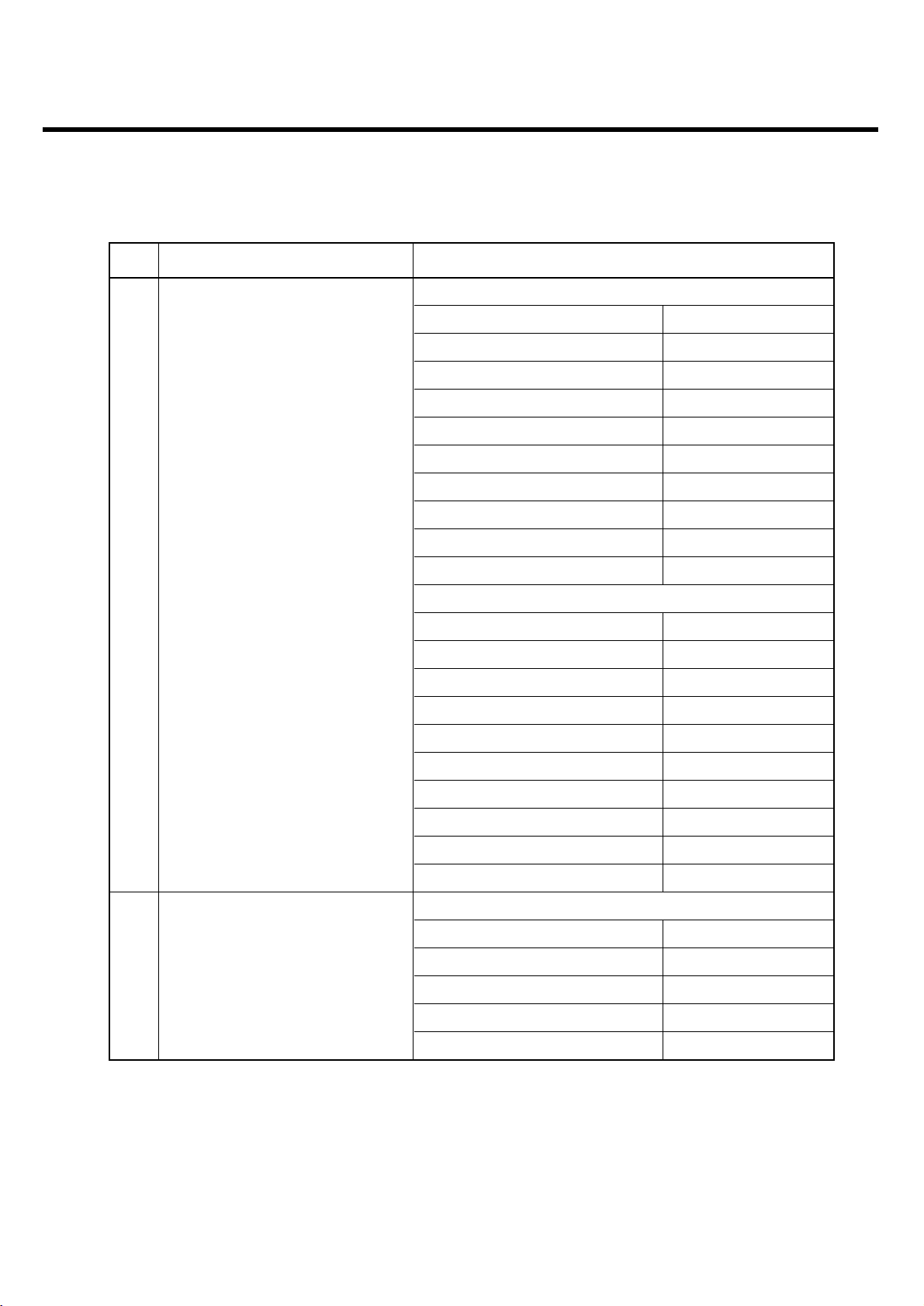
2.1 H/W Features
2. PERFORMANCE
Item Feature Comment
Classification : Li-on
Standard Battery
Capacity min 830mAh
Voltage :3.7V
Cell Weight : 22g
Under the minimum current consumption environment
Stand by Current (such as paging period 9), the level of standby current
is below 4mA.
Talk time Up to 2.5 hours (GSM TX Level 5)
Stand by time Up to 200 hours (Paging Period: 9, RSSI: -85 dBm)
Charging time Approx. Under 3 hours
RX Sensitivity GSM, EGSM: -107dBm, DCS: -107dBm
TX output power
GSM, EGSM: 33dBm(Level 5),
DCS, PCS: 30dBm(Level 0)
GPRS compatibility Class 10
SIM card type 3V Small
Display
Main LCD : 128 x 160 260K TFT, 1.77”
Sub LCD : 96 x 64 65K OLED,1.04”
Hard icons. Key Pad
0 ~ 9, #, *, Up/Down Navigation Key
Status Indicator Menu Key, Clear Key
Send Key, END/PWR Key
Soft Key(Left/Right)
ANT Internal
EAR Phone Jack Yes (mono)
PC Synchronization Yes
Speech coding EFR/FR/HR
Data and Fax Yes
Vibrator Yes
Loud Speaker Yes
Voice Recoding Yes
Microphone Yes
Speaker/Receiver One way dual speaker
Travel Adapter Yes
Bluetooth / USB Yes
MIDI 64 Poly (Mono SPK)
Options Data Kit , CD
Camera Module Yes (VGA, CMOS)
2. PERFORMANCE
- 10 -
2.2 Technical Specification
Item Description Specification
EGSM
TX: 890 + (n-1024) x 0.2 MHz
RX: 935 + (n-1024) x 0.2 MHz (n=975~1024)
DCS
1Frequency Band TX: 1710 + (n-512) x 0.2 MHz
RX: 1805 + (n-512) x 0.2 MHz (n=512~885)
PCS
TX: 1810 + (n-512) x 0.2 MHz
RX: 1905 + (n-512) x 0.2 MHz (n=512~810)
2 Phase Error
RMS < 5 degrees
Peak < 20 degrees
3 Frequency Error < 0.1 ppm
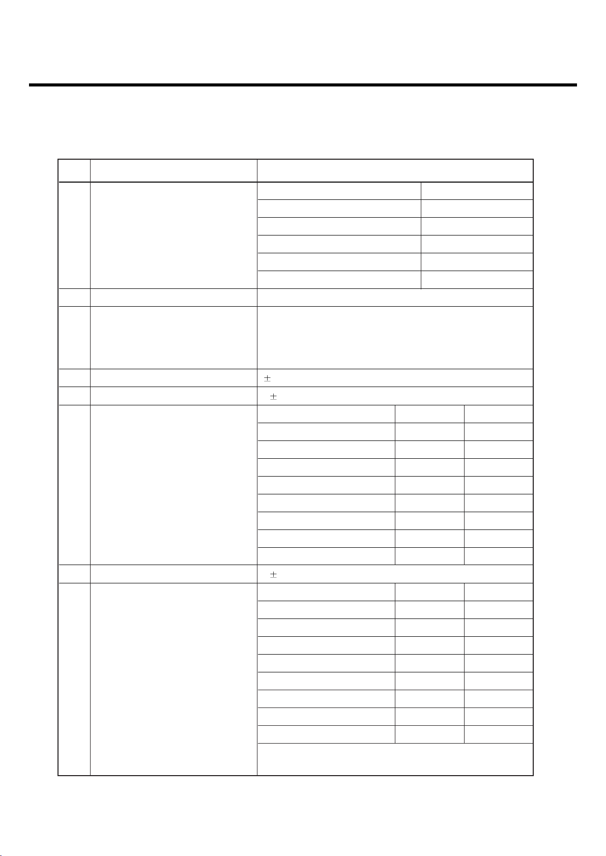
GSM, EGSM
Level Power Toler. Level Power Toler.
5 33 dBm 2dB 13 17 dBm 3dB
6 31 dBm 3dB 14 15 dBm 3dB
7 29 dBm 3dB 15 13 dBm 3dB
8 27 dBm 3dB 16 11 dBm 5dB
9 25 dBm 3dB 17 9 dBm 5dB
10 23 dBm 3dB 18 7 dBm 5dB
11 21 dBm 3dB 19 5 dBm 5dB
4 Power Level 12 19 dBm 3dB
DCS, PCS
Level Power Toler. Level Power Toler.
0 30 dBm 2dB 8 14 dBm 3dB
1 28 dBm 3dB 9 12 dBm 4dB
2 26 dBm 3dB 10 10 dBm 4dB
3 24 dBm 3dB 11 8 dBm 4dB
4 22 dBm 3dB 12 6 dBm 4dB
5 20 dBm 3dB 13 4 dBm 4dB
6 18 dBm 3dB 14 2 dBm 5dB
7 16 dBm 3dB 15 0 dBm 5dB
2. PERFORMANCE
- 11 -
Item Description Specification
GSM, EGSM
Offset from Carrier (kHz). Max. dBc
100 +0.5
200 -30
250 -33
400 -60
600~ <1,200 -60
1,200~ <1,800 -60
1,800~ <3,000 -63
3,000~ <6,000 -65
5
Output RF Spectrum 6,000 -71
(due to modulation) DCS, PCS
Offset from Carrier (kHz). Max. dBc
100 +0.5
200 -30
250 -33
400 -60
600~ <1,200 -60
1,200~ <1,800 -60
1,800~ <3,000 -65
3,000~ <6,000 -65
6,000 -73
GSM, EGSM
Offset from Carrier (kHz) Max. (dBm)
Output RF Spectrum 400 -19
6
(due to switching transient) 600 -21
1,200 -21
1,800 -24
2. PERFORMANCE
- 12 -
Item Description Specification
DCS, PCS
Offset from Carrier (kHz). Max. (dBm)
Output RF Spectrum 400 -22
6
(due to switching transient) 600 -24
1,200 -24
1,800 -27
7 Spurious Emissions Conduction, Emission Status
GSM, EGSM
8 Bit Error Ratio
BER (Class II) < 2.439% @-102 dBm
DCS, PCS
BER (Class II) < 2.439% @-100 dBm
9 RX Level Report Accuracy 3 dB
10 SLR 8 3 dB
Frequency (Hz) Max.(dB) Min.(dB)
100 -12 -
200 0 -
300 0 -12
11 Sending Response 1,000 0 -6
2,000 4 -6
3,000 4 -6
3,400 4 -9
4,000 0 -
12 RLR 2 3 dB
Frequency (Hz) Max.(dB) Min.(dB)
100 -12 -
200 0 -
300 2 -7
500
*
-5
13 Receiving Response 1,000 0 -5
3,000 2 -5
3,400 2 -10
4,000 2
*
Mean that Adopt a straight line in between 300 Hz and
1,000 Hz to be Max. level in the range.
2. PERFORMANCE
- 13 -
Item Description Specification
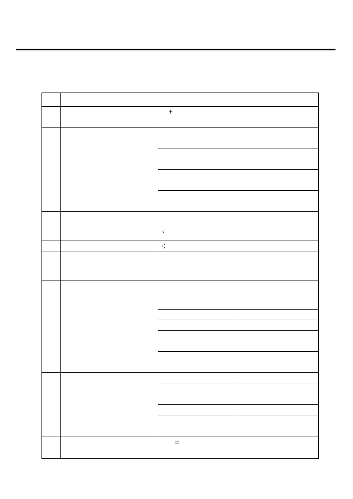
14 STMR 13 5 dB
15 Stability Margin > 6 dB
dB to ARL (dB) Level Ratio (dB)
-35 17.5
-30 22.5
-20 30.7
16 Distortion
-10 33.3
0 33.7
7 31.7
10 25.5
17 Side Tone Distortion Three stage distortion < 10%
18
System frequency
2.5ppm
(13 MHz) tolerance
19 32.768KHz tolerance 30ppm
At least 65 dBspl under below conditions:
20 Ringer Volume 1. Ringer set as ringer.
2. Test distance set as 50 cm
21 Charge Current
Fast Charge : < 450 mA
Pre Charge : < 100 mA
Antenna Bar Number Power
5 -85 dBm ~
4 -90 dBm ~ -86 dBm
22 Antenna Display 3 -95 dBm ~ -91 dBm
2 -100 dBm ~ -96 dBm
1 -105 dBm ~ -101 dBm
0~ -105 dBm
Battery Bar Number Voltage
0 3.51 ~ 3.61 V
23 Battery Indicator 1 3.62 ~ 3.69 V
2 3.70 ~ 3.77 V
3 3.78 ~ 3.91 V
4 3.92 V ~
24 Low Voltage Warning
3.62 0.03V (Call)
3.50 0.03V (Standby)
2. PERFORMANCE
- 14 -
Item Description Specification
25 Forced shut down Voltage 3.35 0.03 V
1 Li-ion Battery
26 Battery Type
Standard Voltage = 3.7 V
Battery full charge voltage = 4.2 V
Capacity: 830mAh
Switching-mode charger
27 Travel Charger Input: 100 ~ 240 V, 50/60 Hz
Output: 5.2 V, 800 mA
3. TECHNICAL BRIEF
- 15 -
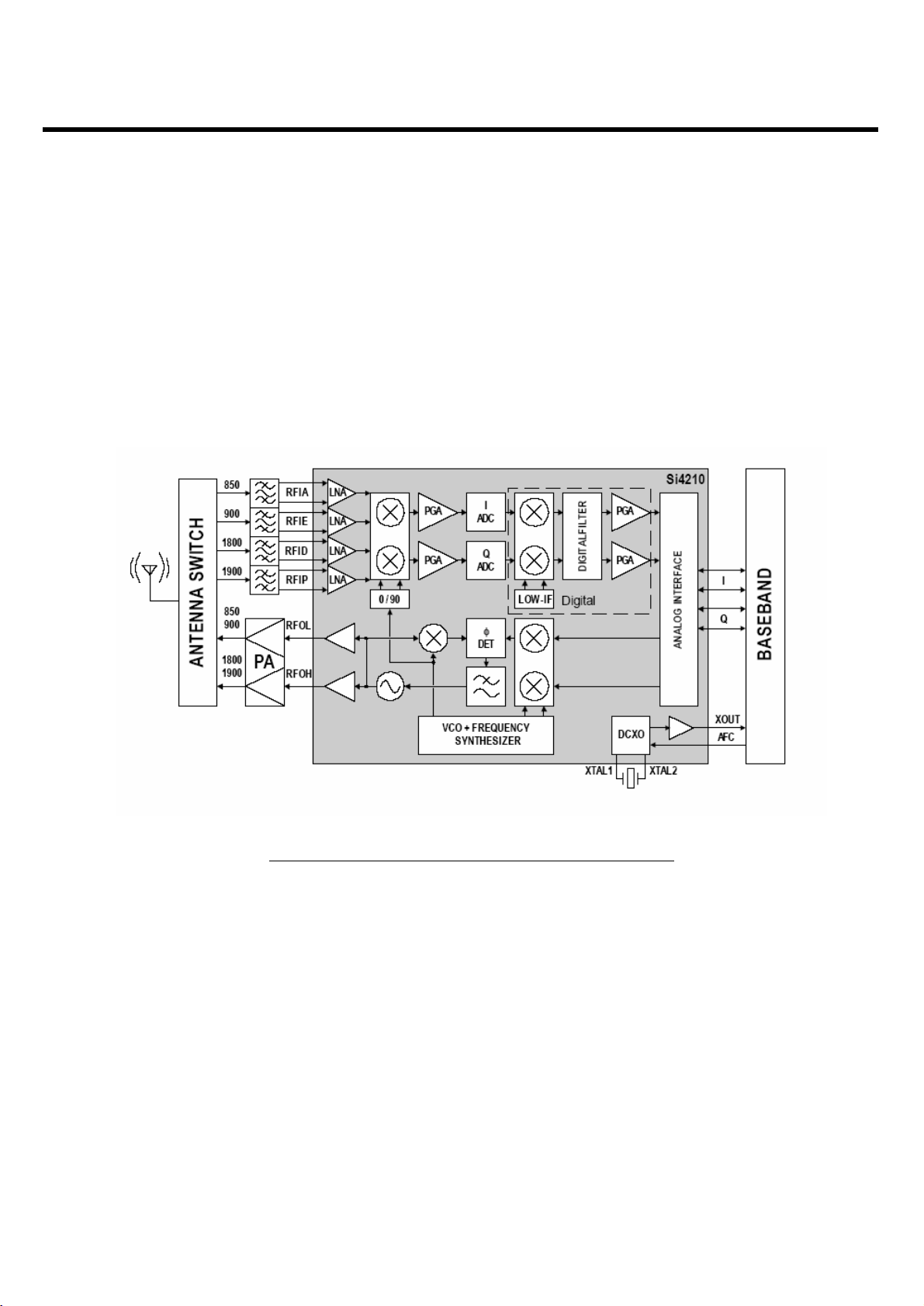
3.1 Transceiver (SI4210, U401)
The RF parts consist of a transmitter part, a receiver part, a frequency synthesizer part, a voltage
supply part, and a VCTCXO part.
The Aero 2 transceiver is the integrated RF front end for multi-band GSM/GPRS digital cellular
handsets and wireless data modems. The integrated solution eliminates the IF SAW filter, external low
noise amplifier (LNAs) for three bands, transmit and RF voltage controlled oscillator (VCO modules,
and other discrete components found in conventional designs.)
3. TECHNICAL BRIEF
Figure. 3-1 RECEIVER FUNCTIONAL BLOCK DIAGRAM
3. TECHNICAL BRIEF
- 16 -
(1) Receiver Part
The Aero 2 transceiver uses a low-IF receiver architecture which allows for the on chip integration of the
channel selection filters, eliminating the external RF image reject filters and the IF SAW filter required in
conventional super-heterodyne architectures.
A. RF front end
RF front end consists of Front End Module(FL400) and dual band LNAs integrated in transceiver (U401).
The Received RF signals(GSM 925MHz ~ 960MHz, DCS 1805MHz ~ 1880MHz PCS 1905MHz ~
1980MHz) are fed into the antenna or Mobile switch.
The Front End Module(FL500) is used to control the Rx and Tx paths. And, the input signals ANT_SW1,
ANT_SW2 of a FL400 are directly connected to baseband controller to switch either Tx or Rx path on.
The logic and current is given below Table 3-1
Three differential-input LNAs are integrated in SI4205. The GSM input supports the GSM 850 (864894MHz) or E-GSM 900 (925-960MHz) bands. The DCS input supports the DCS 1800 (1805-1880 MHz)
band. The PCS input supports the PCS 1900 (1930-1990 MHz) band.
The LNA inputs are matched to the 150 balanced output SAW filters through external LC matching
networks. The LNA gain is controlled with the LNAG[1:0] and LNAC[1:0] bits in register 05h (Figure 3-2).
ANT_SW1 ANT_SW2
GSM Tx 2.5 ~ 3.0 0 V 0V
DCS, PCS Tx 0V 2.5 ~ 3.0 V
GSM Rx 0V 0 V
DCS, PCS Rx 0V 0 V
Table 3-1 THE LOGIC AND CURRENT
3. TECHNICAL BRIEF
- 17 -
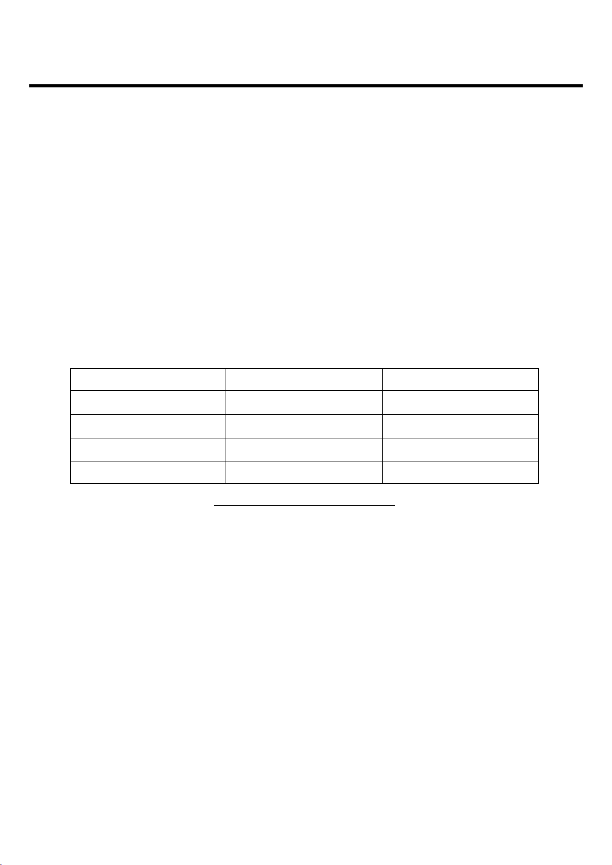
B. Intermediate frequency (IF) and Demodulation
A quadrature image-reject mixer downconverts the RF signal to a 100KHz intermediate frequency (IF) with
the RFLO from the frequency synthesizer. The RFLO frequency is between 1737.8 to 1989.9 MHz, and is
internally divided by 2 for GSM 850 and E-GSM 900 modes. The mixer output is amplified with an analog
programmable gain amplifier (PGA), which is controlled with the AGAIN[2:0] bits in register 05h (Figure3-2).
The quadrature IF signal is digitized with high resolution A/D converters (ADCs).
The ADC output is downconverted to baseband with a digital 100KHz quadrature LO signal. Digital
decimation and IIR filters perform channel selection to remove blocking and reference interference signals.
The selectivity setting (CSEL=0) or a low selectivity setting (CSEL=1). The low selectivity filter has a flatter
group channelization filter is in the baseband chip. After channel selection, the digital output is scaled with a
digital PGA, which is controlled with the DGAIN [5:0] bits in register 05h.
The amplified digital output signal go through with DACs that drive a differential analog signal onto the
RXIP,RXIN,RXQP and RXQN pins to interface to standard analog ADC input baseband ICs. No special
processing is required in the baseband for offset compensation or extended dynamic range.
Compared to a direct-conversion architecture, the low-IF architecture has a much greater degree of
immunity to dc offsets that can arise from RF local oscillator(RFLO) self-mixing, 2nd order distortion of
blockers, and device 1/f noise.
Figure. 3-2 SI4210 RECEIVER PART
3. TECHNICAL BRIEF
- 18 -
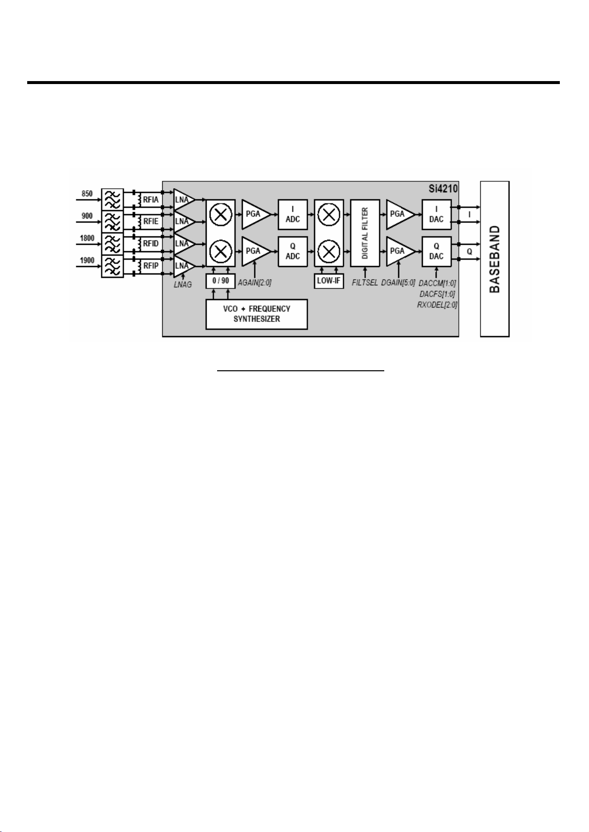
(2) Transmitter Part
The transmit (Tx) section consists of an I/Q baseband upconverter, and offset phase-locked loop (OPLL)
and two output buffers that can drive external power amplifiers (PA), one for the GSM 850 (824-849 MHz)
and E-GSM 900 (880-915 MHz) bands and one for the DCS 1800 (1710-1785 MHz) and PCS 1900 (18501910MHz) bands.
A. IF Modulator
The baseband converter(BBC) within the GSM chipset generates I and Q baseband signals for the Transmit
vector modulator. The modulator provides more than 40dBc of carrier and unwanted sideband rejection and
produces a GMSK modulated signal. The baseband software is able to cancel out differential DC offsets in
the I/Q baseband signals caused by imperfections in the D/A converters. The Tx-Modulator implements a
quadrature modulator. A quadrature mixer upconverts the differential in-phase (TXIP, TXIN) and quadrature
(TXQP, TXQN) signals with the IFLO to generate a SSB IF signal that is filtered and used as the reference
input to the OPLL.
The IFLO frequency is generated between 766 and 896 MHz and internally divided by 2 to generate the
quadrature LO signals for the quadrature modulator, resulting in an IF between 383 and 448 MHz.
For the E-GSM 900 band, two different IFLO frequencies are required for spur management.
Therefore, the IF PLL must be programmed per channel in the E-GSM 900 band.
Figure. 3-3 SI4210 TRANSMITTER PART
3. TECHNICAL BRIEF
- 19 -
B. OPLL
The OPLL consists of a feedback mixer, a phase detector, a loop filter, and a fully integrated TXVCO. The
TXVCO is centered between the DCS 1800 and PCS 1900 bands, and its output is divided by 2 for the
GSM 850 and E-GSM 900 bands. The RFLO frequency is generated between 1272 and 1483 MHz. To
allow a single VCO to be used for the RFLO, high-side injection is used for the GSM 850 and E-GSM 900
bands, and low-side injection is used for the DCS 1800 and PCS 1900 bands. The I and Q signals are
automatically swapped when switching bands. Additionally, the SWAP bit in register 03h can be used to
manually exchange the I and Q signals.
Low-pass filters before the OPLL phase detector reduce the harmonic content of the quadrature modulator
and feedback mixer outputs. The cutoff frequency of the filters is programmable with the FIF[3:0] bits in
register 04h (Figure 3-3), and should be set to the recommended settings detailed in the register
description.
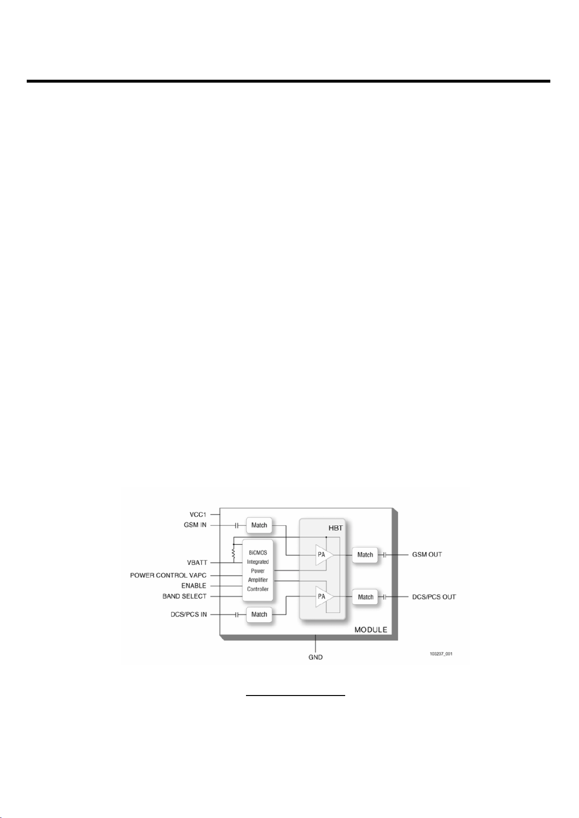
3.2 PAM (SKY77328, U500)
The SKY77328 Power Amplifier Module (PAM) is designed in a low profile (1.2 mm), compact form factor
for quad-band cellular handsets comprising GSM850/900, DCS1800, and PCS1900 operation. The PAM
also supports Class 12 General Packet Radio Service (GPRS) multi-slot operation.
The module consists of separate GSM850/900 PA and DCS1800/PCS1900 PA blocks, impedancematching circuitry for 50 Ω input and output impedances, and a Power Amplifier Control (PAC) block with an
internal current-sense resistor.
Figure. 3-4 SKY77328
3. TECHNICAL BRIEF
- 20 -
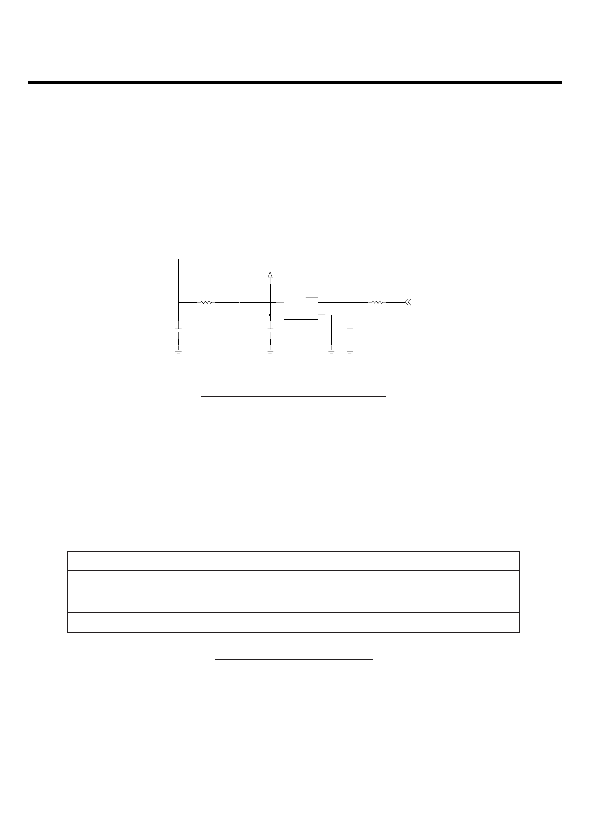
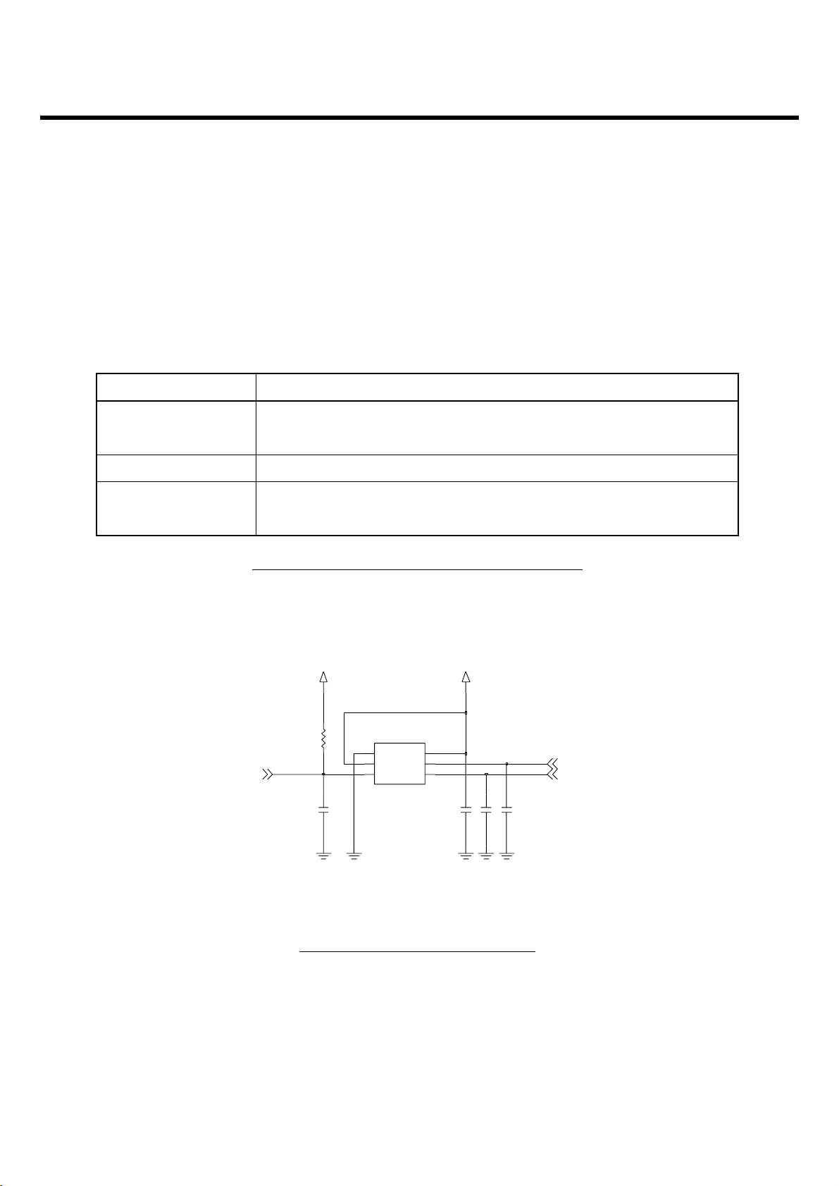
3.3 26 MHz Clock (VCTCXO, X400)
The 26 MHz clock(X400) consists of a VCTCXO(Temperature Compensated Crystal Oscillator) which
oscillates at a frequency of 26 MHz. It is used within the Si4205, analog base band chipset (U101,
AD6537B), digital base band chipset (U102, AD6527)
3.4 Power Supplies for RF Circuits (RF LDO, U403)
Two regulators are used for RF circuits. One is MIC5255 (U403), and the other is one port of AD6537B
(U101). MIC5255 (U403) supplies power to transceiver (SI4210, U401). One port of AD6537B supplies
power to VVCXO (X400). Main power (VBAT) from battery is used for PAM (SKY77328, U400) because
PAM requires high power.
NA
100
C443
R416
1000p
C441
2V75_VVCXO
GND
2
OUT
3
4
VCC
1
VCONT
R417
15K
X400
26MHz
C442
2.2u
AFC
Figure 3-5 VCTCXO CIRCUIT DIAGRAM
Supplier Voltage PowersPowers enabled signal
U403(RF) 2.85 V U401 CLKON
U102(VVCXO) 2.75 V X400
Battery(VBAT) 3.4 ~ 4.2 V U400, U403
Table 3-2 RF POWER SUPPLIERS
3. TECHNICAL BRIEF
- 21 -
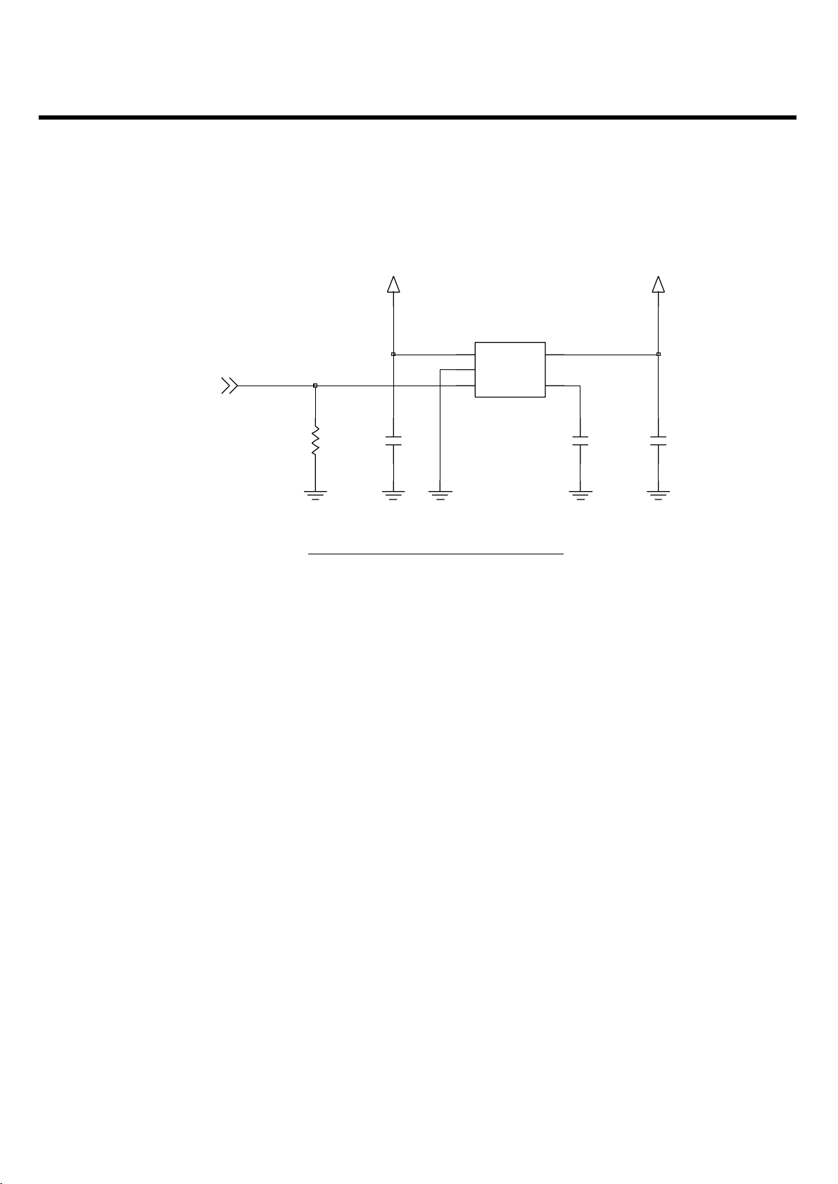
Figure 3-6 RF LDO CIRCUIT DIAGRAM
CLKON
VBAT
U403
1
IN5OUT
2
GND
3
MIC5255-2.85BM5
R419
100K
C444
1u
RF2V85
4
BYPEN
C445
0.01u
C446
4.7u
3. TECHNICAL BRIEF
- 22 -
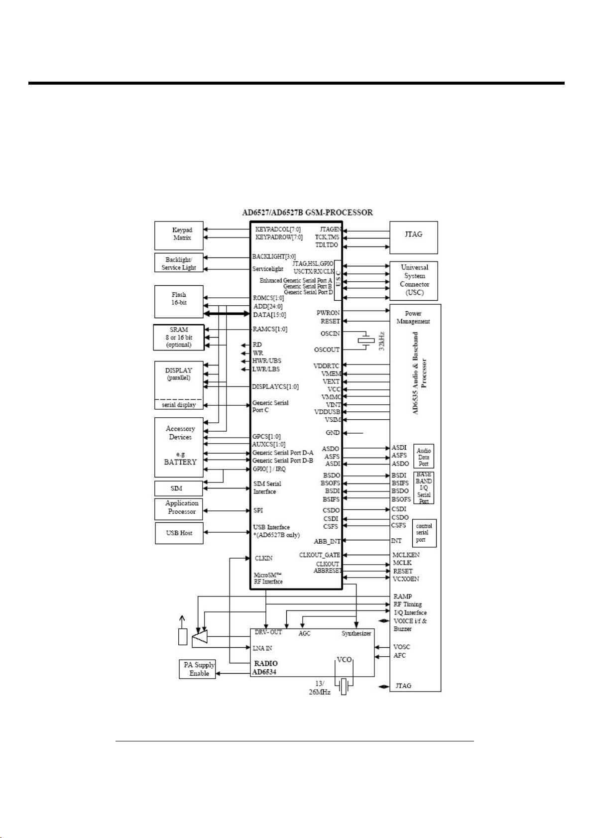
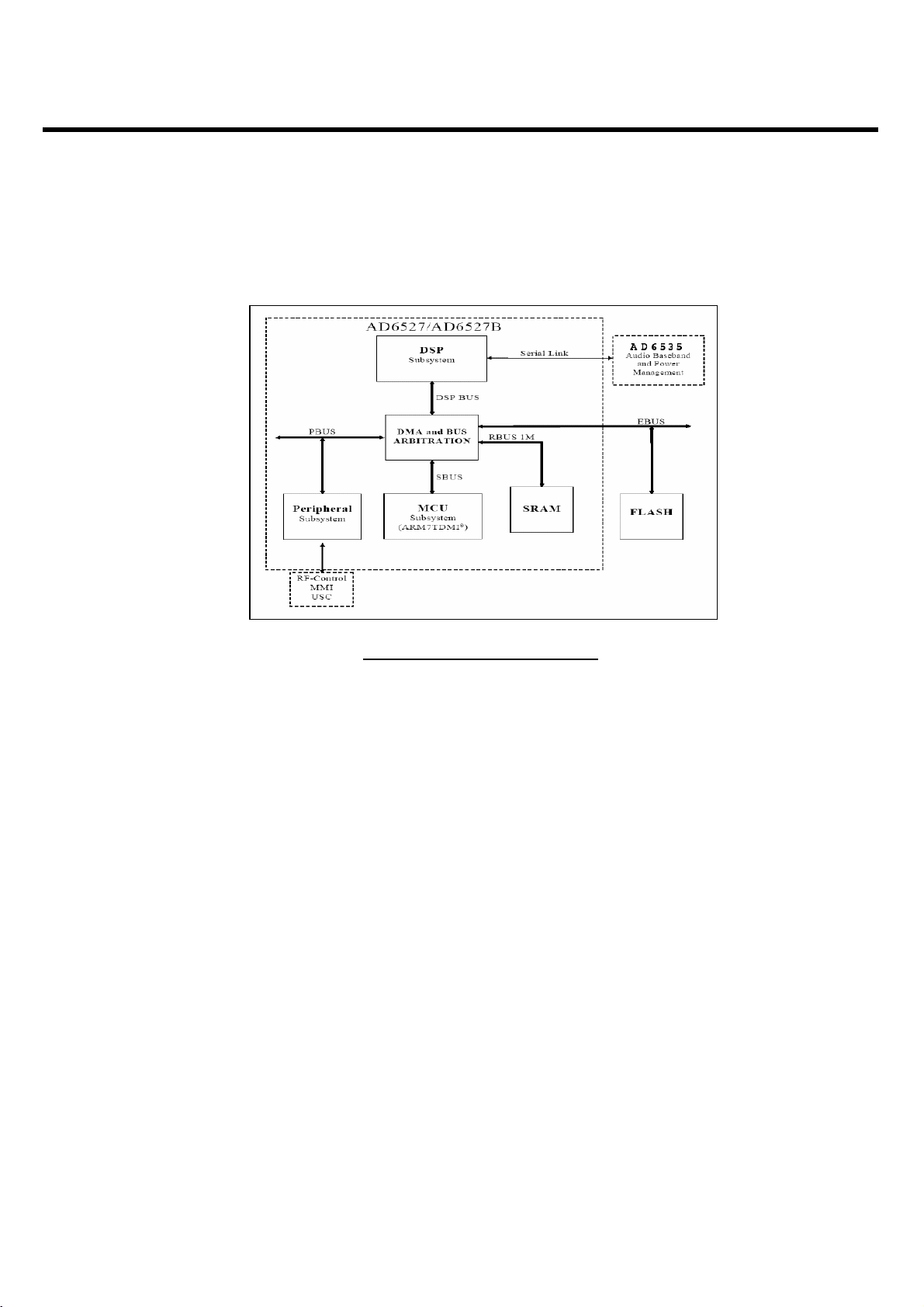
3.5 Digital Main Processor (AD6527, U102)
Figure 3-7. SYSTEM INTERCONECTION OF AD6527 EXTERNAL INTERFACE

3. TECHNICAL BRIEF
- 23 -
• AD6527 is an ADI designed processor.
• AD6527 consists of
1. Control Processor Subsystem
• 32-bit ARM7TDMI Control Processor
• 58.5 MHz operation at 1.7V
• On-board 16KB instruction/Data Cache
• 1 Mbits of on-chip System SRAM
2. DSP Subsystem
• 16-bit Fixed Point DSP Processor
• 91 MIPS at 1.7V
• 16K word Data and 16K word Program SRAM
• 4K word Program Instruction Cache
• Architecture supports Full Rate, Enhanced Full Rate, Half Rate, and AMR Speech
Encoding/Decoding Algorithms
3. Peripheral Subsystem
• Shared on-chip peripheral and off-chip interface:
• Support for Burst and Page Mode Flash
• Support for Pseudo SRAM
• Ciphering module for GPRS supporting GAE1 and GAE2 encryption algorithms
• Parallel and Serial Display Interface
• 8 x 8 Keypad Interface
• Four independent programmable backlight plus One Service Light
• 1.8V and 3.0V, 64 kbps SIM interface
• Universal System Connector Interface
• Slow, Medium and Fast IrDA transceiver interface
• Enhanced Generic Serial Port
• Dedicated SPI interface
• Thumbwheel Interface
• JTAG Interface for Test and In-Circuit Emulation
4. Other
• Supports 13 MHz and 26 MHz Input Clocks
• 1.8V Typical Core Operating Voltages
• 204-Ball LFBGA(mini-BGA) Package
5. Applications
• GSM900/DCS1800/PCS1900/PCS850 Wireless Terminals
• GSM Phase 2+ Compliant
• GPRS Class 12 Compliant
• Multimedia Services(MMS)
• Extended Messaging System(EMS)
3. TECHNICAL BRIEF
- 24 -
3.5.1 Interconnection with external devices
A. RTC block interface
Countered by external X-TAL
The X-TAL oscillates 32.768KHz
B. LCD module interface
The LCD module is controlled by CAMERA IC, CL765A
If CL765A is in the state of by-pass mode, the LCD control signals from AD6527 are by-passed
through CL765A.
In operating mode, the CL765A controls the LCD module through L_MAIN_LCD_CS,
L_SUB_LCD_CS, LCD_RESET, LCD_RS, LCD_WR, LCD_RD, L_DATA[15-00], 2V8_MV,1.8_MV.
Signals Description
L_MAIN_LCD_CS MAIN LCD driver chip enable. MAIN LCD driver IC has own CS pin
L_SUB_LCD_CS SUB LCD driver chip enable. SUB LCD driver IC has own CS pin
LCD_RESET (GPIO 15) This pin resets LCD module. This signal comes from DBB directly.
LCD_WR Enable writing to LCD Driver.
LCD_RD Enable reading to LCD Driver.
LCD_RS This pin determines whether the data to LCD module are display
data or control data. LCD_RS can select 16 bit parallel bus.
2V8_MV,1V8_MV 2.85V voltage is supplied to LCD driver IC.
LCD_SIGNAL1
(GPIO_16)
For the future.
LCD_SIGNAL2
(GPIO_17)
Table 3-3. LCD CONTRON SIGNALS DISCRIPTION
3. TECHNICAL BRIEF
- 25 -
C. RF interface
The AD6527 control RF parts through PA_BAND, ANT_SW1, ANT_SW2, CLKON , PA_EN, SEN,
SDATA, SCLK, RF_PWR_DWN.
D. Key interface
Include 5 column , 5 row and additional GPIO 35 for KEY_ROW5. The AD6527 detects whether key
is pressed or not by using interrupt method.
E. AD6537B Interrupt
AD6537B provides an active-high interrupt output signal. Interrupt signals are generated by the
Auxiliary ADC, audio, and charger modules.
Signals Description
PA_BAND (GPO 17) PAM Band Select
ANT_SW1 (GPO 9) Antenna switch Band Select
ANT_SW2 (GPO 11) Antenna switch Band Select
CLKON RF LDO Enable/Disable
PA_EN (GPO 16) PAM Enable/Disable
S_EN (GPO 19) PLL Enable/Disable
S_DATA (GPO 20) Serial Data to PLL
S_CLK (GPO 21) Clock to PLL
RF_EN (GPO 4) Power down Input
Table 3-5. SIM CONTROL SIGNALS DESCRIPTION
3. TECHNICAL BRIEF
- 26 -
F. SIM interface
The AD6527 provides SIM Interface Module. The AD6527 checks status periodically during
established call mode whether SIM card is inserted or not, but it doesn't check during deep Sleep
mode. In order to communicate with SIM card, 3 signals SIM_DATA, SIM_CLK,
SIM_RST(GPIO_23)
are required. The descriptions about the signals are given by bellow Table 3-6 in detail.
Signals Description
SIM_DATA This pin receives and sends data to SIM card. This model can support
1.8volt and 3.0 volt interface SIM card.
SIM_CLK Clock 3.25MHz frequency.
SIM_RST
Reset SIM block
(GPIO_23)
Table 3-6. SIM CONTRON SIGNALS DISCRIPTION
Figure 3-8. SIM Interface of AD6527
(KDS, 1.6T)
SIM CONNECTOR
C324
NA
C325 22p
R369
20K
2V85_VSIM
1000pC326
J301
CLK
3
GND
4
6
I_O
RST
2
1
VCC
5
VPP
2V85_VSIM
220nC318
SIM_DATA
SIM_RST
SIM_CLK
3. TECHNICAL BRIEF
- 27 -
3.5.2 AD6527 Architecture
The internal architecture of AD6527 is shown above Figure 3-10. AD6527 regroups three main subsystems
connected together through a dynamic and flexible communication bus network. It also includes onboard
system RAM (SRAM) and interfaces with external Flash Memory, Baseband converter functions, and
terminal functions like MMI, SIM and Universal System Connector (USC).
The Digital Signal Processing (DSP) subsystem primarily hosts all the speech processing, channel
equalization and channel codec functions. The code used to implement such functions can be stored in
external Flash Memory and dynamically downloaded on demand into the DSP’s program RAM and
Instruction Cache.
The micro-controller subsystem supports all the GSM terminal software, including the layer 1, 2 and 3 of the
GSM protocol stack, the MMI, and applications software such as data services, test and maintenance. It is
tightly associated with on-chip system SRAM and also includes boot ROM memory with a small dedicated
routine to facilitate the initialization of the external Flash Memory via code download using the on-chip serial
interface to the external Flash Memory interface.
The peripheral subsystem is composed of system peripherals such as interrupt controller, real time clock,
watch dog timer, power management and a timing and control module. It also includes peripheral interfaces
to the terminal functions: keyboard, battery supervision, radio and display. Both the DSP and the MCU can
access the peripheral subsystem via the peripheral bus (PBUS).
For program and data storage, both the MCU subsystem and the DSP subsystem can access the on chip
system SRAM and external memory such Flash Memory. The access to the SRAM module is made through
the RAM Bus (RBUS) under the control of the bus arbitration logic. Similarly, access to the Flash Memory is
through the parallel External Bus (EBUS).
Figure 3-9. AD6527 Architecture
3. TECHNICAL BRIEF
- 28 -
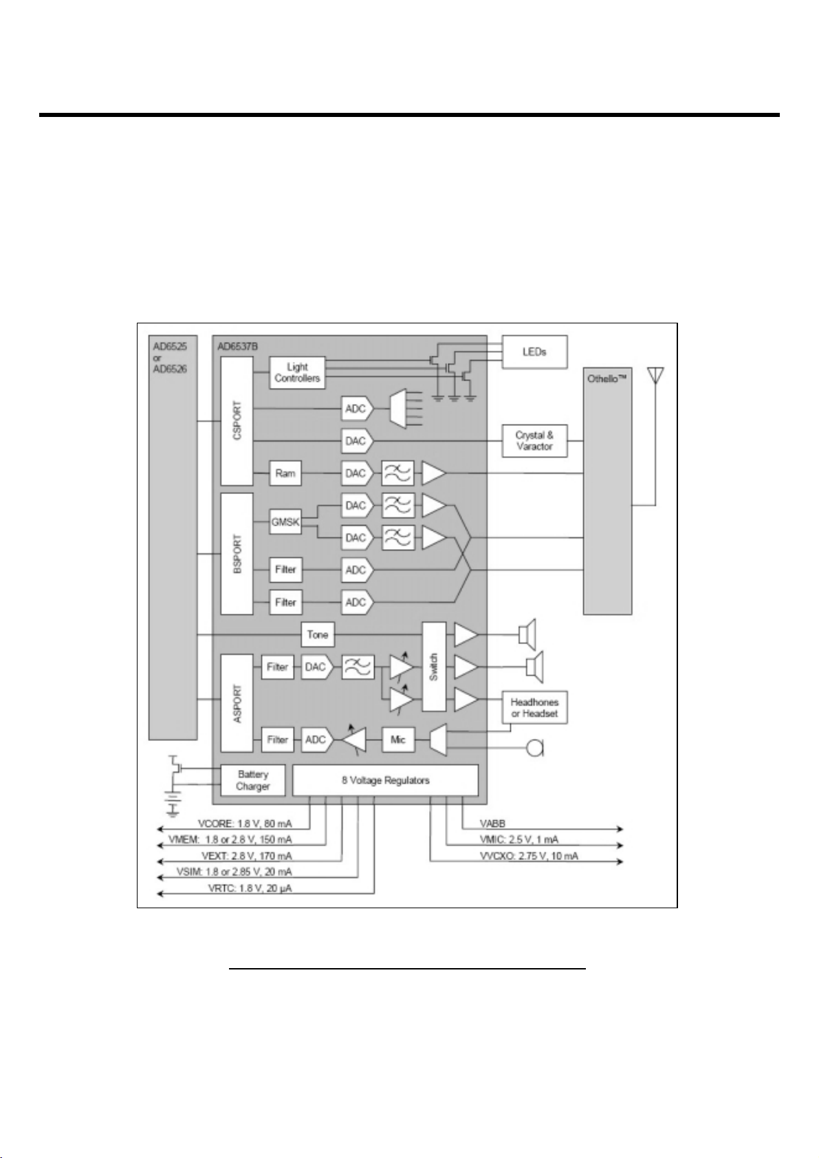
3.6 Analog Main & Power Management Processor
(AD6537B, U101)
Figure 3-10. AD6537B FUNCTIONAL BLOCK DIAGRAM
B

3. TECHNICAL BRIEF
- 29 -
• AD6537B is an ADI designed Analog Baseband processor. AD6537B covers the processing GMSK
modulation interface, Aux ADC, Voice signal processing and Power Management.
• AD6537B consists of
1. BB Transmit section
• GMSK Modulation
• I-channel & Q-channel Transmit DACs and Filters
• Power Ramping DAC
2. BB Receive section
• I-channel & Q-channel Receive ADCs and Filters
3. Auxiliary section
• Voltage Reference
• Automatic Frequency Control DAC
• Auxiliary ADC
• Light Controllers
4. Audio Section
• 8 kHz & 16 kHz Voiceband Codec
• 48 kHz Monophonic DAC
• Power Amplifiers
5. Power Management section
• Voltage Regulators
• Battery Charger
• Battery Protection
6. Digital Processor section
• Control, Baseband, and Audio Serial Ports
• Interrupt Logic
3. TECHNICAL BRIEF
- 30 -
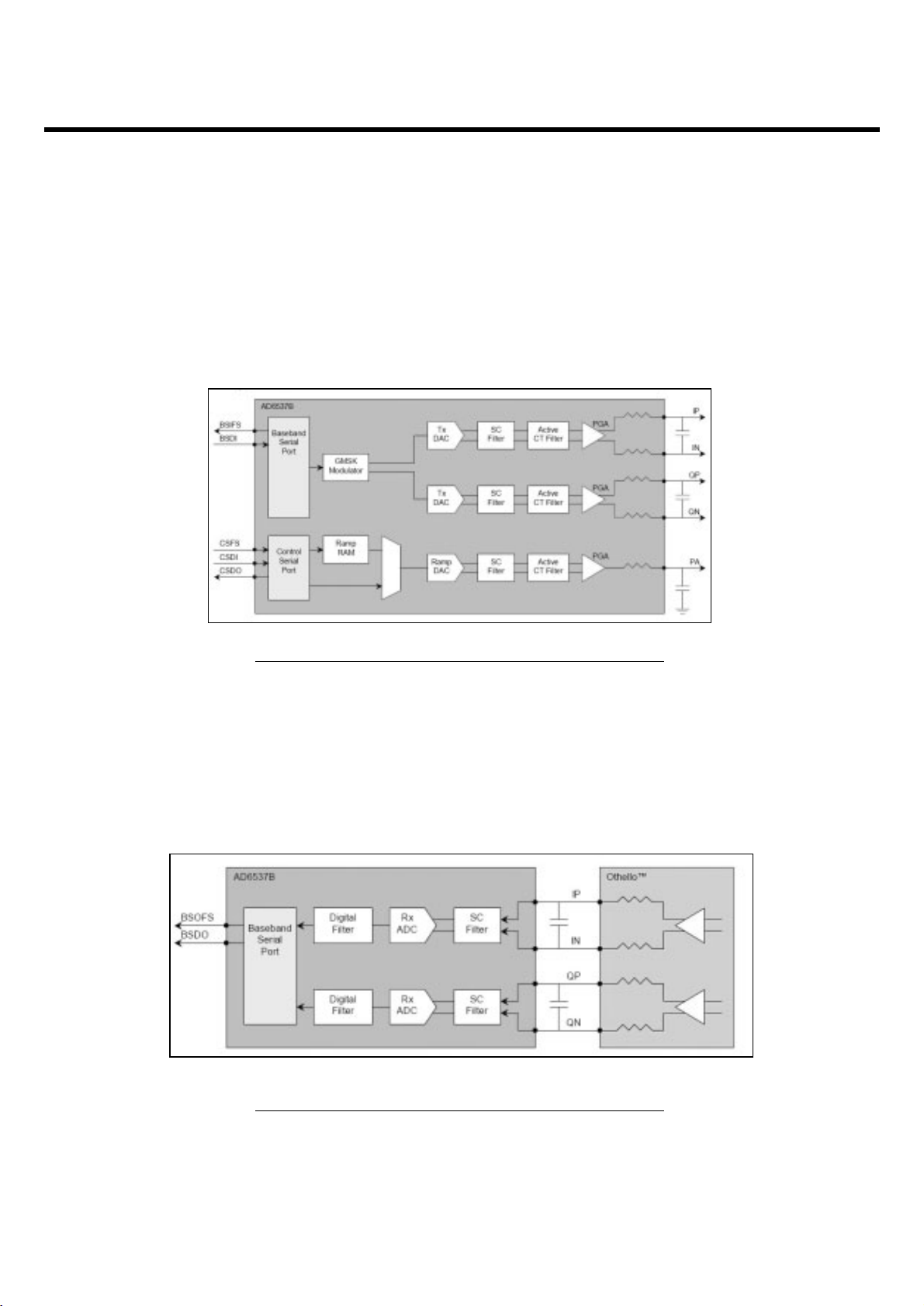
3.6.1 Baseband Transmit Section
1. The AD6537B Baseband Transmit Section is designed to support GMSK for both single-slot and
multi-slot application.
2. The transmit channel consists of a digital GMSK modulator, a matched pair of 10-bit DACs and a
matched pair of reconstruction filter.
3.6.2 Baseband Transmit Section
1. This section consists of two identical ADC channels that process baseband in-phase(I) and
quadrature(Q) input signals.
Figure 3-11. AD6537B BASEBAND TRANSMIT SECTION
Figure 3-12. AD6537B BASEBAND RECEIVER SECTION
3. TECHNICAL BRIEF
- 31 -
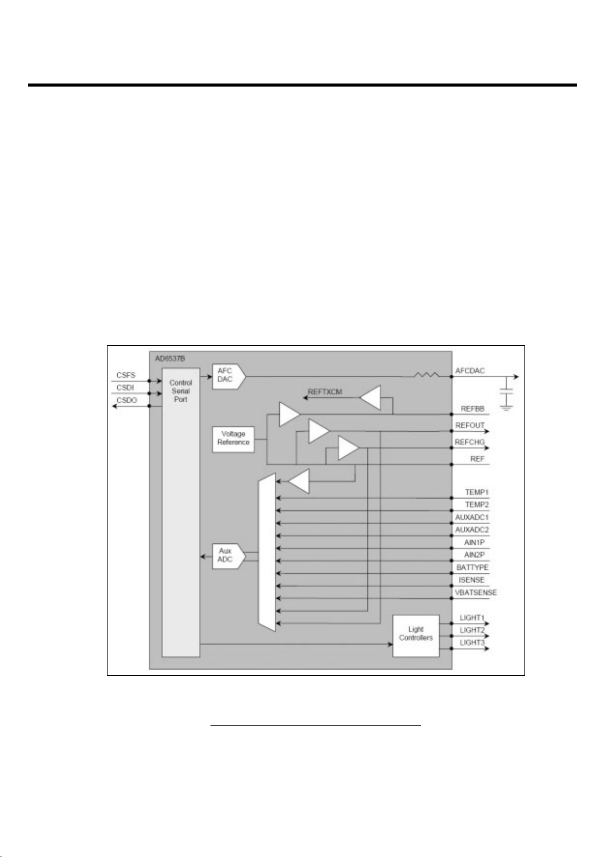
3.6.3 Auxiliary Section
1. This section includes an Automatic Frequency Control(AFC) DAC, voltage reference buffers, an
Auxiliary ADC, and light controllers.
• AFC DAC: 13 bits
2. This section also contains AUX ADC and Voltage Reference
• IDAC: 10 bits
• The Auxiliary ADC provides :
- Two differential inputs for temperature sensing.
- A differential input for the battery charger current sensor
Figure 3-13. AD6537B AUXILIARY SECTION

3. TECHNICAL BRIEF
- 32 -
3.6.4 Audio Section
1. Receive audio signal from microphone. This model uses differential configuration.
2. Send audio signal to speaker. This model uses differential configuration.
3. This section provides an audio codec with a digital-to-analog converter and an analogto-digital
converter, a ring tone volume controller, a microphone interface, and multiple analog input and
output channels.
4. It interconnects with external devices like main microphone, main receiver, and headset. The
descriptions of audio port used in This model are given bellow in detail.
<Up Link>
-AIN1P,AIN1N : Main microphone positive/negative terminal
-AIN2P,AIN2N : Headset microphone positive/negative terminal
-AIN3P,AIN3N : External Analog Input terminal
<Down Link>
-AOUT1P,AOUT1N : Main Speaker positive/negative terminal
-AOUT3P : Headset speaker terminal
Figure 3-14. AD6537B AUDIO SECTION

3. TECHNICAL BRIEF
- 33 -
3.6.5 Power Management
1. Power up sequence logic
1. The AD6537B controls power on sequence
2. Power on sequence
- If a battery is inserted, the battery powers the 8 LDOs.
- Then if PWRONKEY is detected, the LDOs output turn on.
- REFOUT is also enabled
- Reset is generated and send to the AD6527
Figure 3-15. AD6537B POWER MANAGEMENT SECTION

3. TECHNICAL BRIEF
- 34 -
2. LDO Block
1. There are 8 LDOs in the AD6537B.
- VCORE : supplies Digital baseband Processor core and AD6537B digital core (1.8V, 80mA)
- VMEM : supplies external memory and the interface to the external memory on the digital
baseband processor (1,8V or 2.8V, 150mA)
- VEXT : supplies Radio digital interface and high voltage interface (2.8V, 170mA)
- VSIM : supplies the SIM interface circuitry on the digital processor and SIM card
(1.8V or 2.85V, 20mA)
- VRTC : supplies the Real-Time Clock module (1.8 V, 20 µA)
- VABB : supplies the analog portions of the AD6537B
- VMIC : supplies the microphone interface circuitry (2.5 V, 1 mA)
- VVCXO : supplies the voltage controlled crystal oscillator ( 2.75 V, 10 mA)
Figure 3-16. AD6537B POWER MODE LOGIC

3. TECHNICAL BRIEF
- 35 -
3. Battery Charging Block
1. It can be used to charge Lithium Ion and/or Nickel Metal Hydride batteries. Charger initialization,
trickle charging, and Li-Ion charging control are implemented in hardware.
2. Charging Process
- Check charger is inserted or not
- If AD6537B detects that Charger is inserted, the CC-CV charging starts.
- Exception : When battery voltage is lower than 3.2V, the precharge(low current charge mode)
starts firstly.
- And the battery voltage reach to 3.2V the CC-CV charging starts.
3. Pins used for charging
- GATEDRIVE : charge DAC output
- ISENSE : charge current sense input
- VBATSENSE : battery voltage sense input.
- BATTYPE : battery type identification input
- REFCHG : voltage reference output
4. TA (Travel Adaptor)
- Input voltage: AC 85V ~ 260V, 50~60Hz
- Output voltage: DC 5.2V ( 0.2 V )
- Output current: Max 800mA ( 50mA )
5. Battery
- Li-ion battery (Max 4.2V, Nom 3.7V)
- Standard battery: Capacity - 830mAh
Figure 3-17. AD6537B BATTERY CHARGING BLOCK

- 36 -
3. TECHNICAL BRIEF
Figure 3-18.KG245 HEADSET SPEAKER CIRCUIT (AD6537B)
CLOSE TO AD6537B
39p
C144
C139
39p
R109 4.7
T8
SGND1R8SGND2
NC_R12
R12
M2
DGND
C2
GPI
LGND
N15
K16
J16
AOUT3P
AGND1
R16
AIN1N
P16
AIN1P
AIN2N
R15
AIN2P
P15
AIN3R
AOUT1N
K15
AOUT1P
J15
AOUT2N1
T9
AOUT2N2
R9
AOUT2P1
R11
AOUT2P2
T11
AOUT3N
39p
C132
4.7R110
39p
C134
39p
C138
39p
C142
C140
39p
39p
C131 C133
39p
C143
39p
AUXIN
VINNORP
VINNORN
SPKP_P
AUXOP
AUXIP
RCV_N
RCV_P
From Headset
Microphone
To Headset
Speaker
Figure 3-19. KG245 HEADSET SPEAKER CIRCUIT (AD6537B)
CLOSE TO AD6537B
39p
C144
C139
39p
R109 4.7
T8
SGND1R8SGND2
NC_R12
R12
M2
DGND
C2
GPI
LGND
N15
K16
J16
AOUT3P
AGND1
R16
AIN1N
P16
AIN1P
AIN2N
R15
AIN2P
P15
AIN3R
AOUT1N
K15
AOUT1P
J15
AOUT2N1
T9
AOUT2N2
R9
AOUT2P1
R11
AOUT2P2
T11
AOUT3N
39p
C132
4.7R110
39p
C134
39p
C138
39p
C142
C140
39p
39p
C131 C133
39p
C143
39p
AUXIN
VINNORP
VINNORN
SPKP_P
AUXOP
AUXIP
RCV_N
RCV_P
From Main
Microphone
C229
1u
VBAT
IN2
C1
NC1
A1
NC2
C4
NO1
A4
NO2
B4
V+
U204
MAX4684EBC_T
C3
COM1
A3
COM2
B1
GND
C2
IN1
A2
SPK_RCV_N
SPK_RCV_SEL
SPK_RCV_P
SPK_N
SPK_P
RCV_N
RCV_P
To Main
Receiver/
Speaker

3. TECHNICAL BRIEF
- 37 -
In order to reduce time for trickle charging, additional circuit(Pre-charge circuit) was included.
This circuit has supplied Max 160mA current into the battery additionally.
So call it, it reduce trickle charging time
Figure 3-20. CIRCUIT FOR BATTERY CHARGING AT AD6537B
Pre - CHARGING
NORMAL CHARGING
NC_R1
NC_B7
NC_B5
VCHG
T15
R1
R3
T5
G16
B7
B5
B8
A5
A7
A6
NC_T15
VMEMSEL
GND_NET1
NC_G16
VBATSENSE
ISENSE
GATEDRIVE
ONNOFF
R215
10K
C210
1u
VCHARGE
R209
VBAT
ERHY0007007
15
(1%,1/8W)
6
4
R104
0.2
(1%)
Q201
UMX1NTN
C126
1u
D101
(2012)
CUS02
R105 330
Q101
G
S
4
2
1
TPCF8102-TE85L-F
D33D4
D2
D1
1
25
3
D5
D6
R216
1K
5
6
7
8
VBAT
R220
7.5K
VCHARGE
R223
10K
C125
4.7u
VCHG_LED
3
2
Q202
2SC5585
1
R226
20

3. TECHNICAL BRIEF
- 38 -
3.7 LCD MODULE
Controlled by L_MAIN_LCD_CS, L_SUB_LCD_CS, LCD_RESET, LCD_RS,
LCD_WR,LCD_RD,L_DATA[00:17] ports
• L_MAIN_LCD_CS : MAIN LCD driver chip enable. MAIN LCD driver IC has own CS pin
• LCD_RESET : This pin resets LCD module. This signal comes from DBB directly.
• LCD_RS: This pin determines whether the data to LCD module are display data or control data.
• L_WR : Write control Signal
• L_RD : Read control Signal. But this pin used only for debugging.
• L_DATA[00:17] : Parallel data lines.
• LCD_SIGNAL1 : LCD type selection signals
• For using 65K color, data buses should be 16 bits.
Figure 3-21. LCD MODULE CIRCUIT
2V8_C_PWR
VGA CAMERA
128x160 MAIN TFT LCD
96x64 SUB OLED
CONNECTOR(60Pin)
L_DATA00
L_DATA01
L_DATA02
L_DATA03
L_DATA04
L_DATA05
L_DATA06
L_DATA07
LCD_RESET
L_MAIN_LCD_CS
L_SUB_LCD_CS
LCD_WR
LCD_RS
C_SDA
C_SCK
C_RST
OLED_ON
BACK_BATT
MOTOR
ICVE21184E150R500FRFL601
1
INOUT_B1
INOUT_A1
2
INOUT_A2
INOUT_B2
3
INOUT_A3
INOUT_B3
4
INOUT_B4
INOUT_A4
G110G2
5
FL603 ICVE21184E150R500FR
1
INOUT_A1
INOUT_B1
2
INOUT_A2
INOUT_B2
3
INOUT_A3
INOUT_B3
4
INOUT_A4
INOUT_B4
G15G2
10
R603
100
C601
0.1uF
C613
C612
56p
56p
ICVE21184E150R500FR
FL606
1
INOUT_A1
INOUT_B1
2
INOUT_B2
INOUT_A2
3
INOUT_A3
INOUT_B3
4
INOUT_B4
INOUT_A4
G110G2
5
ICVE21184E150R500FRFL608
1
INOUT_B1
INOUT_A1
2
INOUT_B2
INOUT_A2
3
INOUT_B3
INOUT_A3
4
INOUT_B4
INOUT_A4
G1
G2
C614
5
10
56p
4.7KR602
R601 4.7K
9
8
7
6
9
8
7
6
9
8
7
6
9
8
7
6
27pC604
LCD_ID
SPK_RCV_P
SPK_RCV_N
VCHG_LED
FLASH_LED
MLED
R604 100K
27p
C602
2V8_VEXT
VCHARGE
2V8_C_PWR
(60pin, Socket, 1.5T, 0.4mm)
AXK760145J
CN601
1
60
2
59
3
58
57
4
56
5
55
6
54
7
53
8
52
9
10
51
11
50
12
49
13
48
14
47
15
46
16
45
17
44
18
43
19
42
20
41
21
40
22
39
23
38
24
37
25
36
26
35
27
34
28
33
29
32
30 31
1uC605
27pC603
C606 1u
VBAT
IFMODE
MLED1
MLED2
MLED3
C607
1u
FL602
FL604
FL607
1
INOUT_A1
2
INOUT_A2
3
INOUT_A3
4
INOUT_A4
1
INOUT_A1
2
INOUT_A2
3
INOUT_A3
4
INOUT_A4
5
INOUT_A5
6
INOUT_A6
1
INOUT_A1
2
INOUT_A2
3
INOUT_A3
4
INOUT_A4
1
INOUT_A1
2
INOUT_A2
3
INOUT_A3
4
INOUT_A4
1
INOUT_A1
2
INOUT_A2
3
INOUT_A3
4
INOUT_A4
ICVE21184E150R500FR
9
INOUT_B1
8
INOUT_B2
7
INOUT_B3
6
INOUT_B4
G110G2
5
ICVE31186E150R101FR
13
INOUT_B1
12
INOUT_B2
11
INOUT_B3
10
INOUT_B4
9
INOUT_B5
8
INOUT_B6
G17G2
14
ICVE21184E150R500FRFL605
9
INOUT_B1
8
INOUT_B2
7
INOUT_B3
6
INOUT_B4
G110G2
5
ICVE21184E150R500FR
9
INOUT_B1
8
INOUT_B2
7
INOUT_B3
6
INOUT_B4
G110G2
5
ICVE21184E150R500FRFL609
9
INOUT_B1
8
INOUT_B2
7
INOUT_B3
6
INOUT_B4
G110G2
5
C608
C609
56p
56p
L_DATA08
L_DATA09
L_DATA10
L_DATA11
L_DATA12
L_DATA13
L_DATA14
L_DATA15
L_DATA16
L_DATA17
C_MCLK
C_PCLK
C_HS
C_VS
C611
C610
56p
56p
C_CD00
C_CD01
C_CD02
C_CD03
C_CD04
C_CD05
C_CD06
C_CD07

3. TECHNICAL BRIEF
- 39 -
3.8 Camera
The CL765A contains various highly-advanced functions such as fully-hardwired JPEG codec, image scaler
for Digital Zoom Function, MJPEG codec, high-speed Image data processing, OSD and so on. For the
system level ingegration, the CL765A provides various off-chip interfaces including CMOS/CCD camera
sensor interface, LCD interface, SD card interface and CCIR601/656 interface for external TV encoder
interface.
Figure 3-22. CL765A BLOCK DIAGRAM

3. TECHNICAL BRIEF
- 40 -
A.Camera Interface : Allows you to use the built-in camera to take photos with the phone . The phone
encodes up to 640 x 480 size with free size support.
B.U503 : Camera back-end IC. Camera signal is delivered from Camera Sensor to Camera IC(Q501).
C. Q501,U503,U502 : Regulator for U503 and Camera sensor.
Figure 3-23. CL761 CAMERA IC CIRCUIT
2V85_VCAM
2V8_C_PWR
Q501
SI1305-E3
D
C506
C505
10u
0.1u
L_MAIN_LCD_CS
L_SUB_LCD_CS
S
L_DATA00
L_DATA01
L_DATA02
L_DATA03
L_DATA04
L_DATA05
L_DATA06
L_DATA07
L_DATA08
L_DATA09
L_DATA10
L_DATA11
L_DATA12
L_DATA13
L_DATA14
L_DATA15
L_DATA16
L_DATA17
LCD_WR
LCD_RD
LCD_RS
G
J1
L6
M7
M6
GPIO_0H3GPIO_1H1GPIO_2
L2
L_RESET_N
L10
L_DA0
J9
L_DA1
K10
L_DA2
H8
L_DA3
H9
L_DA4
J10
L_DA5
G10
L_DA6
G9
L_DA7
G8
L_DA8
F8
L_DA9
F10
L_DA10
E10
L_DA11
F9
L_DA12
D10
L_DA13
E9
L_DA14
C10
L_DA15
H2
L_DA16
G1
L_DA17
L1
L_CS_N
K2
L_WR_N
K1
L_RD_N
K3
L_ADS
K9
LS_CS_N
TEST_EN
T_MODE0
SCAN_EN
M_SA0D8M_SA1
M_SD0A7M_SD1
M_8BIT
M_ADS
B7
D9
C8
B10
R508
100K
ADD01
ADD01
ADD02
DATA00
DATA01
CAMERA CTL IC
2V85_VCAM
100KR504
100KR502
100KR503
C_CD06
C_CD07
J8
L3
M10
C9
B8
G2
C_D7
STROBE
C_PWDN
CIS_TYPE0
CIS_TYPE1
CIS_TYPE2
U503
EUSY0240501
(Core Logic, CL761A)
M_SD2A6M_SD3B6M_SD4C6M_SD5A4M_SD6B4M_SD7
M_SD8B3M_SD9
C4
C3
DATA02
DATA03
DATA04
DATA05
DATA06
DATA07
DATA08
DATA09
C_CD05
K8
M9
C_D5L9C_D6
M_SD10D3M_SD11
A3
DATA10
C_CD04
C2
DATA11
C_CD01
C_CD02
C_CD03
C_D2M8C_D3L8C_D4
M_SD12
M_SD13E3M_SD14C1M_SD15
B1
DATA12
DATA13
DATA14
L7
C_CD00
M5
C_D0K7C_D1
E2
DATA15
C_SCK
C_SDA
M4
C_SCK
C_SDA
M_CS_N
_RD
_LCD_CS
C_PCLK
L4
C_PCLK
M_WR_N
F3
_WR
C_HS
C_RST
K4
M3
C_HS
C_RST
M_HOLDE1M_INTRD1M_RD_NG3M_RESET_N
F1
CAM_INT
CAM_HOLD
C_VS
M1
M2
C_VS
A9
CAM_RST
C_MCLK
VDDS
C_MCLK
VDDL
VDDI1
VDDI2
VDDC1
VDDC2
VDDC3
VDDC4
1608
GNDI1
GNDI2
GNDI3
GNDI4
GNDC1
GNDC2
GNDC3
GNDC4
GNDC5
XOUT
MS_CS_N
_SUB_CS
K5
J2
B9
C7
A8
A10
D2
H10
B2
E8
J3
K6
A5
B5
C5
F2
L5
A2
XIN
A1
R509
100K
CAMERA/MIDI LDO
ONNOFF
2V85_VCAM
C510
C509 C511
C508
C507
0.1u
1u
1u
0.01u
C515
4.7u
WHITE/FLASH LED LDO
C516
0.01u
26MHz
C_FLASH
LCD_DIM_CTL
1V8_MIDI_COREVBAT
2V85_VCAM
U501
10
VIN1VOUT1
2
9
VOUT2
EN1
3
8
EN2
NC3
4
7
BYP
NC2
6
GND
11
5
C501
C502
1u
0.01u
BGND
NC1
MIC2211-GOYML
C503
C504
1u
10u
(1.8V=150mA, 2.85V=300mA)
1u
VBAT
C517
4.7u
R506
1.5K
R511
1.5K
R512
R507
1K
1K
1uC513
C512 1u
11
12
14
C1-
C1+
C2+
4
VIN
9
U502
GND
17
16
EN_FLSH
10
EN_SET
AAT2807AIXN-4.5
C514 1u
15
2
C2-
VOUT_FL
VOUT_BL
C3+
ISINK1
ISINK2
ISINK3
1
C3-
3
13
8
NCPGND
5
6
7
C519
C518
1u
1u
FB501
FB502
MLED1
MLED2
MLED3
R505
FLASH_LED
22
MLED

3. TECHNICAL BRIEF
- 41 -
3.9 Keypad Switch and Scanning
The key switches are metal domes, which make contact between two concentric pads on the keypad layer of
the PCB when pressed. There are (Normal Key 24EA, Camera side key, Volume up down side key),
connected in a matrix of 5 rows by 5 columns and additional GPIO 35 for KEY_ROW5, as shown in Figure 324, except for the power switch (KB1), which is connected independently. Functions, the row and column
lines of the keypad are connected to ports of AD6527. The columns are outputs, while the rows are inputs
and have pull-up resistors built in.
When a key is pressed, the corresponding row and column are connected together, causing the row input to
go low and generate an interrupt. The columns/rows are then scanned by AD6527 to identify the pressed
key.
Figure 3-24. Keypad Switches and Scanning
5
2
SEND
7
1
*
3
RIGHT
4
CAMERA
CONF
#
VOL_UP
UP
DOWN
CLR
VOL_DOWN
MENU
LEFT
0
Side Key
6
9
FAV
8
SEL
T
END
EVL14K02200
VA303
680
R354
R333 680
SW329
SW325
680R352
SW321
100
R318
SW310
SW311
EVL14K02200
VA306
SW315
S71PL256NC0_TLA084
SW317
680R323
R331 680
R301
10K
SW309
SW318
680
EVL14K02200
VA301
R332
SW314
R322 680
VA302
EVL14K02200
R319
100 100
R320
VA305
EVL14K02200
SW326
680R324
SW312
SW306
SW324
SW322
VA307
EVL14K02200
SW328
VBAT
SW308
R356 680
R321
100
SW316
4
5
CN602
1
2
3
R343 680
SW313
SW327
SW323
SW307
SW319
680R349
R302 680
SW320
KEY_ROW2
KEY_ROW5
KEY_COL1
KEY_COL0
KEY_COL4
KEY_ROW1
KEY_COL3
KEY_ROW3
KEY_ROW4
KEY_COL2
KEY_ROW0
POWERKEY

3. TECHNICAL BRIEF
- 42 -
3.10 Microphone
The microphone is placed to the front cover and contacted to main PCB. The audio signal is passed to AIN1P
and AIN1N pins of AD6537B. The voltage supply VMIC is output from AD6537B, and is a biased voltage for
the AIN1P. The AIN1P and AIN1N signals are then A/D converted by the voiceband ADC part of
AD6537B.The digitized speech (PCM 8KHz ,16KHz) is then passed to the DSP section of AD6527 for
processing (coding, interleaving etc).
3.11 Main Speaker
In the case of G692 , there are 3 different speakers. One is main speaker for the received voice, another are
loud speaker for playback of ring tone , key tone and other MIDI sounds and the other is headset speaker.
The main speaker is driven directly from AD6537B AOUT1P and AOUT1N pins and the gain is controlled by
the PGA in an AD6537B. The receiver is placed in the folder cover and connected to AOUT1x terminal via
FPCB.
Figure 3-25. Connection between Microphone and AD6537B
2V5_VMIC
R202
1K
39p
C208
39p
C218
39p
C204
10u
C212
39p
EVL5M02200
VA202
VA201 EVL5M02200
MIC
(BSE, -42dB, FPCB Type)
VINNORP
VINNORN
C211
39p
R210 100
R206
2.2K
100R217
0.1uC215
R221
2.2K
C217
CLOSE TO MIC

3. TECHNICAL BRIEF
- 43 -
3.12 Headset Interface
This phone chooses a 6 pin type headset which has 6 electrodes such as GND, AUXIP, AUXIN (this pin is
floating), AUXOP, JACK_DETECT, HOOK_DETECT. This type supports mono sound.
Switching from Receiver to Headset Jack
If jack is inserted, JACK_DETECT goes from high to low.
Audio path is switched from receiver to earphone by JACK_DETECT interrupt.
Switching from Headset Jack to Receiver
If jack is removed, JACK_DETECT goes from low to high.
Audio path is switched from earphone to receiver by JACK_DETECT interrupt.
Hook detection
If hook-button is pressed, HOOK_DETECT is changed from high to low.
This is detected by AD6527(GPIO_36).
And then hook is detected.
Figure 3-26. HEADSET JACK INTERFACE
CLOSE TO EARJACK
AUXIN
JACK_DETECT
(GPIO_45)
C203
0.1u
AUXOP
AUXIP
VA203
2V8_VEXT
C201
0.1u
EVL5M02200
C209
C216 0.1u
NA
2V5_JACK
R201
1K
C206
22u
R204
1.5K
C219
39p
VA204
33uC214
R225
1M
EVL5M02200
HOOK_DETECT
(GPIO_39)
C220
39p
U201
1
GND
NC
VOUT
Vin
NCP563Q25T1
4
32
J201
7502-2.5G-SB1-A
(3 pole, ENJE0003501)
2V5_JACK
C202
10u
(1608)

3. TECHNICAL BRIEF
- 44 -
3.13 Key Back-light Illumination
In key back-light illumination, there are 14 Blue LEDs in Main Board, which are driven by
KEY_BACKLIGHT signal from AD6527.
Figure 3-27. KEY BACK-LIGHT ILLUMINTION
1uC301
C302 1u
C303 1u
KEY_BACKLIGHT
1u
C304
VBAT
75
75
R304
R303
C306 1u
C307 1u
C305 1u
LD301
LD302
LEBB-S14H
LEBB-S14H
KEY BACKLIGHT
75
75
R305
LD303
LEBB-S14H
R306
LD304
LEBB-S14H
R307
LD305
75
R308
LD306
LEBB-S14H
75
R309
LD307
LEBB-S14H
75
LEBB-S14H
VBAT
R310 75
LD308
LEBB-S14H
75R311
LD309
LEBB-S14H
75R312
LD310
LEBB-S14H
75R313
LD311
LEBB-S14H
R314 75
LD312
LEBB-S14H
R315 75
LD313
LEBB-S14H
75R316
LD314
LEBB-S14H
1u
C308
C309
1u
1u
C312
C313
1u
C314
1u
1u
1u
C310
C311
Q301
31
R325
12K
R328
12K
C316
27p
R329
R330
10
10
2
UMX1NTN
4
56
C315
27p
R326
R327
10
10

3. TECHNICAL BRIEF
- 45 -
3.14 VIBRATOR
The vibrator is placed in the folder cover and contacted to LCD MODULE. The vibrator is driven from
VIBRATOR (GPIO_3) of AD6527.
Figure 3-28. MOTOR
VIBRATOR
VIBRATOR
VBAT
R350
20
R353
1.5K
R357
7.5K
Q302
23
1
EMZ2
VBAT
R334
47K
R351
220
5
64
C317
4.7u
MOTOR

3.15 Bluetooth Section Description (M201)
1) U203(BH28FB1WHFV) : Provide power for bluetooth block
2) U205(TC7SH08FS) : PCM Sync Clock rate converter for bluetooth clock(8kHZ)
3) U206(MAX4717EBC-T) : Analog switch for bluetooth block
4) M201(LBMA-2C67B2) : Bluetooth module
3. TECHNICAL BRIEF
- 46 -
Figure 3-29. BLUETOOTH CIRCUIT
BLUETOOTH
BT_EN
2V8_VBT
U205
TC7SH08FS
1
3
PCM_TX
USC3
VBAT 2V8_VBT
L201
NA NA
VDD_1_8V
ANT
VDD_DIG
VDD_VREGIN
GND1
GND2
GND3
GND4
UART_TX
UART_RX
UART_RTS
UART_CTS
PCM_IN
PCM_OUT
PCM_SYNC
PCM_CLK
R227
0
22
21
3
4
6
11
25
27
24
23
26
19
17
18
20
U203
R228
330
C232
0.1u
C236
0.1u
5
VCC
4
GND
2
C231
2.2u
PCM_EN
USC1
USC2
C230
15p
PCM_SYNC8
R240
VIN VOUT
3
2
1
2V8_VMEM
C2
IN1
A2
IN2
C3
COM1
A3
COM2
10K
BGND
GND
STBY
BH28FB1WHFV
B4
V+
NO1
NO2
NC1
NC2
GND
B1
4
6
NC
5
C233
C234
2.2u
15p
RESETB
PIO0
PIO1
PIO2
PIO3
PIO4
PIO5
NC
SPI_CLK
SPI_CSB
SPI_MOSI
SPI_MISO
5
M201
LBMA-2C67B2
C237
NA
16
1
2
7
8
9
10
28
13
14
12
15
_BT_RST
C240
0.1u
C4
PCM_RX
A4
PCM_TX
C1
USC_1
A1
USC_2 PCM_SYNC8
U206
MAX4717EBC-T
C248
L202
22nH
R235 47
R238 47
ANT201
GND1
FEED
GND2
AMAN542015LG02
(SNGF0008801)
C249
15p
47R232
DEBUG_RX
47R233
DEBUG_TX
PCM_TX
47R236
PCM_RX
47R237
USC0
2V8_VBT
C238
2.2u
C239
2.2u

3. TECHNICAL BRIEF
- 47 -
3.16.1 Bluetooth Circuit Description (M201)
1. Bluetooth Module Features
- Output power(Class2): 1.0 dBm Typ.
- Receiver Sensitivity: -83 dBM Max.
- Dimensions: 6.9 * 7.9 * 1.5 (unit: mm)
- Wide operating temperature range(Target): -40 to85C (Storage: -40 to 100C)
- D.C Supply voltage range: 1.8V or 3.0V(Nominal)
- Interfaces: UART and SPI for data and PCM for voice
- Stack layer: HCI or RFCOMM
- Compatibility with Bluetooth Specification 1.2
Figure 3-30. BLUETOOTH INTERFACE

4. TROUBLE SHOOTING
- 48 -
4.1 RF Component
4. TROUBLE SHOOTING
SW400
FL400
U400
U401
X400
U403
U402
Mobile Switch
Sw400
FEM
Fl400
VVCXO,26MHz Clock
X400
2.85V Regulator
U403
Inerter
U402
RF Main Chip(SI4210)
U401
Power Amp Module(SKY77328)
U400
Figure 4-1. RF Component

4. TROUBLE SHOOTING
- 49 -
4.2 RX Trouble
START
(1) Check
regulator circuit
Redownload SW or
Do calibration again
HP8960 : Test mode
62 CH, 7 level setting (TCH)
62CH, -60dBm setting (BCCH)
Spectrum analyzer setting
Oscilloscope setting
(2) Check
VCTCXO
(3) Check
Mobile SW
&FEM
(4) Check
RX IQ
CHECKING FLOW

(1) Checking Regulator Circuit
4. TROUBLE SHOOTING
- 50 -
TEST POINT
CIRCUIT
CHECKING FLOW
Figure 4-2 (a). Regulator Circuit
Figure 4-2 (b). Regulator Circuit
U403. 3
(EN)
U403
U403. 5
(OUT)
CLKON
VBAT
U403
1
IN5OUT
2
GND
3
MIC5255-2.85BM5
R419
100K
C444
1u
4
BYPEN
C445
0.01u
RF2V85
C446
4.7u
Voltage at
Pin5 of U403
Is 2.85V?
YES
Regulator Circuit is OK
See next Page to check
VCTCXO
NO
Level at
Pin3 of U403
Is high?
YES
Replace U403
NO
Change main board

4. TROUBLE SHOOTING
- 51 -
(2) Checking VVCXO Circuit
X400.3
(OUT)
X400.4
(VCC)
X400
Check Pin 3.
Refer to Graph 4-1(b)
26 MHzO.K?
No
No
VVCXO Circuit is OK
See next Page to check
Mobile SW
See next Page to check
Mobile SW
Yes
Check Pin 4.
Refer to Graph 4-1(a)
2.75V OK?
No
Yes
Changing X400
Check U101, PMIC
NA
100
C443
R416
1000p
C441
2V75_VVCXO
GND
2
OUT
3
4
VCC
1
VCONT
R417
15K
X400
26MHz
C442
2.2u
AFC
Figure 4-3 (a). VVTXO Circuit
Figure 4-3 (a). VVTXO Circuit
TEST POINT
CIRCUIT
CHECKING FLOW
WAVEFORM
Graph 1(a)
Graph 1(b)

(3) Checking Mobile SW & FEM
4. TROUBLE SHOOTING
- 52 -
TEST POINT
CIRCUIT WAVEFORM
ANT_SW1 ANT_SW2
GSM_TX High Low
DCS_TX Low High
RX Low Low
Figure 4-4(a) Mobile SW & FEM Circuit
ANT SW Control GSM& DCS RX Mode
Graph 2
Table 1Figure 4-4 (b). Mobile SW & FEM Circuit
SW400.ANT
SW400.RF
VC_DCSPCS
VC_EGSM
FL400
SW400
(GPIO_11)
(GPIO_9)
270p
C440
NA
L400
C417
22p
6
GND3
GND4
7
16
GND5
GND6
17
18
GND7
GND8
19
20
GND9
14
PCS_RX1
PCS_RX2
15
VC_DCSPCS
3
VC_EGSM
9
ANT
1
DCSPCS_TX
5
12
DCS_RX1
DCS_RX2
13
10
EGSM_RX1
EGSM_RX2
11
8
EGSM_TX
2
GND1
GND10
21
22
GND11
GND12
23
24
GND13
4
GND2
FL400
HWXQ511
1p
C407
ANT400
C418
ANT
G1
G2
RF
NA
KMS-506
SW400
ANT401
270p
C439
L407
5.6nH
NA
C410
ANT402
ANT_SW1
ANT_SW2
FL301. 10
VC1
VC2
Low
Low
VC_DCSPCS
Low
Low
Low
Low
VC_EGSM

4. TROUBLE SHOOTING
- 53 -
ANT_SW1 ANT_SW2
GSM_TX High Low
DCS_TX Low High
RX Low Low
Table 4-2
CHECKING FLOW
Check C439,C440
Check whether Ant SW
Set as RX mode
RRefer to Table 4-2
Yes
VC1 :Low
VC2 :Low
Check SW400 Pin ANT,RF
with RF Cable connected.
Open
Yes
Changing SW400
Check SW400 Pin ANT,RF
with No RF Cable Connected
Short
Yes
Changing SW400
For these 2 test case,
No Call connection is needed
No
No
Changing the Board.
Check RF Level of
FL500.10 (for GSM) &
FL500.1(for DCS)
Ant SW & Mobile SW is OK
See next Page to check
Rx IQ Signal
Pin10 : ~ -62dBm
Pin 1 : ~ -63dBm
No
Changing FL400
Yes
No
For this RF Level test case,
RX Stand alone Mode is needed
refer to chapter 11

(4) Checking RX IQ
4. TROUBLE SHOOTING
- 54 -
TEST POINT
CIRCUIT
WAVEFORM
C425
C427
U401
C427 1.5p
C426 1.5p
5.6nH
L403
C423 2p
XMODE
XTAL1
30
XTAL2
RESET
RFIDP
22
RFIEN
21
RFIEP
18
RFIPN
17
RFIPP
RFOH
16
15
RFOL
12
VDD1
VDD2
1328
VDD3
VDD4
29
VIO
11
XDIV
26
25
AFC
27 14
GND
24
RFIAN
23
RFIAP
20
RFIDN
19
U401
SI4210
C428 12p
C425 1.8p
L404
6.8nH
CHECKING FLOW
Redownload software and calibration again
Similar?
No
Replace U401
Yes
No
Check C425,C427.
Check if there is any
Major difference
Refer to graph 4-3
Figure 4-5 (a). RX IQ Circuit
Figure 4-5 (b). RX IQ Circuit
Graph 3

4. TROUBLE SHOOTING
- 55 -
4.3 TX Trouble
CHECKING FLOW
START
(1)Check
regulator circuit
Redownload SW or
Do calibration again
HP8960 : Test mode
62 CH, 7 level setting (TCH)
62CH, -60dBm setting (BCCH)
Spectrum analyzer setting
Oscilloscope setting
(2)Check
VVCXO
(4)Check
PAM control
signal
(5)Check
TX IQ
(3)Check
Mobile SW
& FEM

(1) Checking Regulator Circuit
4. TROUBLE SHOOTING
- 56 -
TEST POINT
CIRCUIT
U403. 5
(OUT)
U403. 3
(EN)
U403
Figure 4-6 (a). Regulator Circuit
RF2V85
VBAT
0.01u
C445
R419
100K
C444
1u
4
BYPEN
3
GND
2
1
IN5OUT
MIC5255-2.85BM5
U403
C446
4.7u
CLKON
CIRCUIT
Regulator Circuit is OK
See next Page to check
VVCXO
Voltage at
Pin5 of U403
Is 2.85V?
Level at
Pin3 of U403
Is high?
YES
NO
Replace U403
YES
NO
Change main board
Figure 4-6 (b). Regulator Circuit

(2) Checking VVCXO Circuit
4. TROUBLE SHOOTING
- 57 -
TEST POINT CHECKING FLOW
Figure 4-7 (a). VVCXO Circuit
X400.3
(OUT)
X400.4
(VCC)
X400
CIRCUIT
Figure 4-7 (b). VVCXO Circuit
Graph 4(a)
NA
100
C443
R416
1000p
C441
2V75_VVCXO
GND
2
OUT
3
4
VCC
1
VCONT
R417
15K
X400
26MHz
C442
2.2u
AFC
WAVEFORM
Graph 4(a)
Check Pin 3.
Refer to Graph 4-1(b)
26 MHzO.K?
No
No
VVCXO Circuit is OK
See next Page to check
Mobile SW
See next Page to check
Mobile SW
Yes
Check Pin 4.
Refer to Graph 4-1(a)
2.75V OK?
No
Yes
Changing X400
Check U101, PMIC

(3) Checking Mobile SW & FEM
4. TROUBLE SHOOTING
- 58 -
TEST POINT
CIRCUIT WAVEFORM
Figure 4-8 (a). SW & FEM Circuit
SW400.AN
T
SW400.RF
VC_DCSPCS
VC_EGSM
FL400
SW400
(GPIO_11)
(GPIO_9)
270p
C440
NA
L400
C417
22p
6
GND3
GND4
7
16
GND5
GND6
17
18
GND7
GND8
19
20
GND9
14
PCS_RX1
PCS_RX2
15
VC_DCSPCS
3
VC_EGSM
9
ANT
1
DCSPCS_TX
5
12
DCS_RX1
DCS_RX2
13
10
EGSM_RX1
EGSM_RX2
11
8
EGSM_TX
2
GND1
GND10
21
22
GND11
GND12
23
24
GND13
4
GND2
FL400
HWXQ511
1p
C407
ANT400
C418
ANT
G1
G2
RF
NA
KMS-506
SW400
ANT401
270p
C439
L407
5.6nH
NA
C410
ANT402
ANT_SW1
ANT_SW2
Graph 5(a) GSM Tx mode
Graph 5(b) DCS,PCS Tx mode

4. TROUBLE SHOOTING
- 59 -
CHECKING FLOW
Check SW400.ANT, RF with RF
Cable connected.
Open
Yes
Changing SW400
Check SW400.ANT,RF
with RF Cable disconnected
Short
Yes
Changing SW400
No
No
Check C439,C440
Check whether Ant SW
Set as TX mode
RRefer to Graph4-6
RRefer to Table 6-11
Yes
Check VC_EGSM,
VC_DCSPCS
Check RF Level of
FL400 Pin 5 (for GSM) & Pin 3 (for
DCS)
Pin5 : ~29.5dBm
Pin 3 : ~26.5dBm
No
Yes
No
Changing board
Go to 4.3.5 Checking PAM
control signal
END
For the test,
TX Stand alone Mode is needed. Refer to
chapter 11 (PL=7 for GSM, PL=2 for DCS)
ANT SW VC_EGSM VC_CDSPCS
DCS TX 0 1
EGSM TX 1 0
EGSM, DCS RX 0 0
Table 4-3

(4) Checking PAM Control Signal
4. TROUBLE SHOOTING
- 60 -
TEST POINT WAVEFORM
Figure 4-9 (a). PAM Control
U400
R606 (PA_EN)
CIRCUIT
Figure 4-9 (b). PAM Control
(GPIO_16)
(GPIO_17)
C406
27p
C404
22u
R606 100
VBAT
R605 100
C405
27p
18
ENABLE
1
BS
PA_BAND
PA_EN
CHECKING FLOW
Go to Next Step
Similar?
Yes
No
Check TX_RAMP and PA_EN
Check if there is
Any Major Difference or not
Refer to Graph 4 - 7
Go to Next Step
Similar?
Yes
No
Go to Next Step
Similar?
Yes
No
Redownload S/W
Check TX_RAMP and PA_EN
Check if there is
Any Major Difference or not
Refer to Graph 4 - 7
Graph 6

4. TROUBLE SHOOTING
- 61 -
(5) Checking TX IQ
TEST POINT
CIRCUIT
Figure 4-10 (b). TX IQ
C427 1.5p
C426 1.5p
5.6nH
L403
C423 2p
XMODE
XTAL1
30
XTAL2
_RESET
RFIDP
22
RFIEN
21
RFIEP
18
RFIPN
17
RFIPP
RFOH
16
15
RFOL
12
VDD1
VDD2
1328
VDD3
VDD4
29
VIO
11
XDIV
26
25
AFC
27 14
GND
24
RFIAN
23
RFIAP
20
RFIDN
19
U401
SI4210
C428 12p
C425 1.8p
L404
6.8nH
CHECKING FLOW
Redownload the Software
And calibrate
Check if there is
Any
Major Difference
Refer to Graph 4
-8
Similar?
Yes
No
Replace U101
WAVEFORM
Figure 4-10 (a). TX IQ
U401
C425
C427
Graph 7

4.4 Power On Trouble
4. TROUBLE SHOOTING
- 62 -
TEST POINT
CIRCUIT
C115
(1V8_VRTC)
C113
(1V8_VCORE
)
C114
(2V8_VMEM)
C119
(2V75_VVCXO)
C118
(2V5_VMIC)
C116
(2V85_VSIM)
(1608)
C116 1u
1V8_VRTC
C122 1u
2V5_VMIC
VBAT
P1
VCORE1
VCORE2
N1
A4
VEXT1
VEXT2
B4
VMEM1
T3
T2
VMEM2
N16
VMIC
VRTC
T7
T6
VSIM
D16
VVCXO
VABB
H16
VBAT_NET
T4
NC_E15
E15
NC_E16
E16
F16
NC_F16
1V8_VCORE
2V8_VEXT
C118 1u
2V85_VSIM
2.2uC117
0.1uC115
C119 1u
R102 1K
2V75_VVCXO
1u
2V75_VABB
C113
C114
2V8_VMEM
1u
BACK_BATT
Figure 4-11(a). Power On Trouble
Figure 4-11(b). Power On Trouble

4. TROUBLE SHOOTING
- 63 -
CHECKING FLOW
START
Check Battery Voltage
> 3.35V
Push power-on key
And check the level change
of PWRKEY
Check the voltage of
The LDO outputs at U101
Logic level at KEYON of U101
= HIGH
Does it work properly?
THE PHONE WILL
POWER ON.
Charge or Change Battery
Check the contact of power key
Or dome-switch
Replace U101
VCORE=1.8V VVCXO=2.75V
VMEM=2.8V VRTC=1.8V
VEXT=2.8V VSIM=1.8V or 2.85V
VABB=2.75V VMIC=2.5V
Re-download software
The power-on procedure is
Completed. The problem may
be elsewhere.
Does it work properly?
Replace the main board
YES
YES
YES
YES
YES
NO
NO
NO
NO
NO
NO

4. TROUBLE SHOOTING
- 64 -
4.5 Bluetooth Section Trouble Shooting
M201
R232
(DEBUG_RX)
R233
(DEBUG_TX)
R236
(PCM_RX)
R235
(PCM_TX)
R237
(PCM_SYNC8)
R238
(USC0)
R227
(ANT)
BLUETOOTH
(SNGF0008801)
2.2u
C239
15p
C234
22nH
L202
2.2u
C238
R238 47
47R236
VBAT 2V8_VBT
L201
NA NA
C248
C231
2.2u
2V8_VMEM
R240
10K
47R233
C233
2.2u
ANT201
FEED
GND1
GND2
0.1u
AMAN542015LG02
C232
47R237
BH28FB1WHFV
U203
6
BGND2GND
NC5STBY
1
3
VIN VOUT
4
R227
0
R228
330
A4
NO2
B4
V+
R235 47
U206
MAX4717EBC-T
C3
COM1
A3
COM2
B1
GND
C2
IN1
A2
IN2
C1
NC1
A1
NC2
C4
NO1
C240
0.1u
47R232
15p
C249
NA
C237
2V8_VBT
2V8_VBT
0.1u
C236
23
24
UART_RX
UART_TX
27
22
VDD_1_8V
VDD_DIG
21
VDD_VREGIN
3
PCM_CLK
PCM_IN
19
PCM_OUT
17
18
PCM_SYNC
PIO0
1
2
PIO1
PIO2
7
8
PIO3
PIO4
9
10
PIO5
16
RESETB
SPI_CLK
13
14
SPI_CSB
SPI_MISO
15
12
SPI_MOSI
26
UART_CTS
UART_RTS
LBMA-2C67B2
M201
ANT
5
4
GND1
6
GND2
GND3
11
GND4
25
28
NC
20
4
5
VCC
U205
TC7SH08FS
2
GND
1
3
15p
C230
USC1
USC2
DEBUG_RX
USC3
PCM_SYNC8
PCM_TX
PCM_RX
_BT_RST
PCM_RX
PCM_TX
USC_1
USC_2 PCM_SYNC8
PCM_TX
USC0
PCM_EN
BT_EN
DEBUG_TX
TEST POINT
CIRCUIT
Figure 4-12(a). Bluetooth Section Trouble Shooting
Figure 4-12(b). Bluetooth Section Trouble Shooting

4. TROUBLE SHOOTING
- 65 -
Checking flow
Bluettooth Power on
IS _BT_RST signal
shape similar FIG.1
Yes
2V8_VBT at
C233 =2.8V ?
Yes
No
No
2V8_VBT at C233,
C234 =2.8V ?
Yes
Check PCB
pattern
Replace U101
Replace U102
No
BT_EN at
R228 =2.8V ?
Yes
Replace
U207
No
Replace
U102

4. TROUBLE SHOOTING
- 66 -
Yes
Yes
No
No
Replace U101
Resolder
Replace U101
Replace M201
Connect BT Headset
Yes
Not available
IF RF level at Antenna
Feeding about 0dBm?
Yes
Replace Headset
No
Is soldering of R239,
L202 good?
Yes
Replace
M201
No
Resolder

4. TROUBLE SHOOTING
- 67 -
Establish a call
Yes
IIS PCM_RX signal
shape similar FIG.3
Yes
Software
Re_download
No
No
Replace U102
Replace M201

4. TROUBLE SHOOTING
- 68 -
4.6 Charging Trouble
D101
R104
Q101
R105
CIRCUIT DIAGRAM
CIRCUIT
(1%)
(2012)
VBAT
VCHARGE
VCHG
VMEMSEL
R3
VBATSENSE
B8
A5
NC_B5
B5
NC_B7
B7
G16
NC_G16
R1
NC_R1
T15
NC_T15
GATEDRIVE
A6
T5
GND_NET1
A7
ISENSE
R104
0.2
C126
1u
S
5
Q101
TPCF8102-TE85L-F
D1
1
D2
2
D33D4
6
D5
7
D6
8
G
4
R105 330
4.7u
C125
CUS02
D101
Figure 4-13(a). Charging Trouble
Figure 4-13(b). Charging Trouble

4. TROUBLE SHOOTING
- 69 -
Checking Flow
START
I/O Connector(CN301)
Is well-soldered ?
YES
Voltage at anode of
D101 = 5.2V ?
YES
Q101,D101, R104 are
well-soldered?
YES
Voltage across R104 is
about 10~100mV?
YES
0.7V < voltage(R105) < 1.3V?
YES
Battery is charged?
NO
NO
NO
NO
NO
NO
Resolder the CN301
Pin 4,5 : VCHARGE
Pin12,19 : GND
The TA is out of order
Change the TA
Resolder the
Q101, D101, R104
Replace the
Q101, D101
Replace the
Q101
The battery may have
problems.
Change the battery.
YES
Charging is
properly operating

4. TROUBLE SHOOTING
- 70 -
4.7 Vibrator Trouble
Soldering Check in LCD Module
+-
R357
Q302
R350
R334
R353
C317
TEST POINT
VIBRATOR
23
64
1
5
Q302
EMZ2
VBAT
VBAT
R357
7.5K
R351
220
C317
4.7u
47K
R334
20
R350
R353
1.5K
MOTOR
VIBRATOR
CIRCUIT
Figure 4-14(a). Vibrator Trouble
Figure 4-14(b). Vibrator Trouble

4. TROUBLE SHOOTING
- 71 -
Checking Flow
SETTING : Enter the engineering mode, and set vibrator on at vibration of BB test menu
START
Is the voltage at pin 3
of Q302 high ?
YES
Is the voltage at pin 2
of Q302 low ?
YES
Is the voltage at pin 1
of Q302 high ?
YES
Check the soldering
of CN601 ?
YES
Check the soldering
of vibrator ?
NO
NO
NO
NO
NO
Check the soldering
of R353, R357
YES
Check the soldering
of R334
YES
Check the soldering
of R351
YES
Replace Q302
NO
Resolder R353, R357
NO
Resolder R334
NO
Resolder R351
Resolder CN601
Resolder vibrator
YES
Replace vrbrator
YES
Vibrator
Working well !

4. TROUBLE SHOOTING
- 72 -
4.8 LCD Trouble
TEST POINT
Figure 4-15(a). LCD Trouble
Figure 4-15(b). LCD Trouble
CN601
FL602
FL601
FL604
FL609
FL605
FL607
FL603 FL606 FL608
LCD Module connection
connector( 60Pin, female )
Camera Module connection
Connector ( 20Pin, female )
LCD Module

4. TROUBLE SHOOTING
- 73 -
CHECKING FLOW
START
Is the connection of
FPCB with connector on
PCB(CN601) ok ?
YES
NO
Reassemble FPCB with CN601 connector
Check the connection LCD
module with connector
On FPCB ?
NO
Reassemble LCD module with connector on FPCB
Check the soldering of
CN601 ?
NO
Change the FPCB and try again
YES
YES
YES
Check the soldering of
EMI filter ?
Resoldering CN601
NO
Resoldering EMI filter(FL600~FL609)
Does LCD work
properly ?
NO
Replace LCD module
YES
LCD working well !
YES

4. TROUBLE SHOOTING
- 74 -
4.9 Camera Trouble
TEST POINT
Figure 4-16(a). Camera Trouble
Figure 4-16(b). Camera Trouble
U503
Q501
FL605
FL609
FL608
FL607
Camera Module
Camera Module
Connector
( 20Pin, male )

4. TROUBLE SHOOTING
- 75 -
CHECKING FLOW
START
Does the LCD itself
Has no trouble ?
YES
NO
Replace the Q501
Change the camera
module, Does it work
properly ?
YES
Itís camera moduleís problem
Replace the camera module
Check the voltage
of pin 3 of
U406 is 3V ?
Check the voltage of pin 22 of
CN601 if 3V ?
YES
Check the signals of the
FL605~FL608
YES
Check the signals of the
FL605~FL608
YES
Camera will work properly
YES
NO
Check the voltage
of pin 1 of
Q501 LOW ?
NO
YES
Go to the LCD trouble
Replace the U503
NO
Check the soldering
of CN601 ?
NO
Replace the Q501
NO
Does the image
appears on LCD ?
YES
YES
Camera will work properly
Replace
FL605~FL608
NO

4. TROUBLE SHOOTING
- 76 -
4.10 Speaker Trouble
Checking Flow
CIRCUIT
Soldering Check
C246
(SPOUT2)
C245
(SPOUT1)
U207
(EUSY0291001)
64 POLY MIDI IC(MP3 Ringtone)
22n
C243
NA
R241
C222
0.1u
0.1u
C228
C224
4.7u
C242
390p
4.7u
C221
R230
6.8K
82K
R239
0.1u
C223
VBAT
A8
SPOUT1_B7
SPOUT2
A7
C8
SPVDD
B8
SPVSS
TESTI0
D6
TESTI1
F6
TESTI2
G6
TESTI3
C7
C2
TXOUT
B2
VREF
_CS__SS
H4
E7
_IRQ
_RD_SI
G4
_RST
D3
J5
_WR_SCK
IOVDD1
E8
H3
IOVDD2
LED0
H8
H7
LED1
J7
LED2
F7
LRCK
MCLK
E6
G7
MTR
MTR_G7
J8
D2
PLLC
RXIN
C3
RXIN_C3
A1
SDIN
F8
H5
SMODE
SO
J6
SPOUT1
B7
DVSS1D1DVSS2D8DVSS3
J4
B4
EQ1
EQ2
A3
A4
EQ3
A2
EXC
C4
EXTIN
C6
EXTOUT
GPIO
H6
HPC
B3
B6
HPOUTL
A6
HPOUTR
HPVSS
A5
G5
IFSEL
D4
INDEX
BBL
B5
BBR
C5
BCLK
G8
CLKI
E2
G3
D0
D1
J2
D2
H2
D3
G2
H1
D4
J1
D4_H1
F3
D5
G1
D6
D7
F2
D7
DVDD1E1DVDD2J3DVDD3
U207
YMU792
F1
A0
E3
A1
AVDD
C1
AVSS
B1
0.1u
C226
C227
0.1u
47p
C247
0.033u
C244
1V8_MIDI_CORE
47p
C246
C250
100p
C251
0.1u
C235
2200p
FB201
2V85_VCAM
20K
R242
47p
C245
C225
0R229
4.7u
0.01u
C241
24K
R234
SPKP_P
SPKP_P
SPK_P
ADD01
SPK_N
_MIDI_RST
26MHz
_MIDI_CS
ADD00
_WR
_RD
DATA05
DATA06
DATA07
DATA00
DATA01
DATA02
DATA03
DATA04
_MIDI_IRQ
Figure 4-17(a). Speaker Trouble
Figure 4-17(b). Speaker Trouble
4. TROUBLE SHOOTING
- 77 -
CHECKING FLOW
START
Check the soldering of
C245, C246
Yes
Check the state of
contact of dual mode speaker
Speaker
Working well!!
Yes
Voltage across C223
= 1.8V?
Check the signal level of
C245, C246
No
Yes
Replace C223
Check the soldering of
C223
No
Yes
Re-soldering
C223
Re-solder C245,
C246 or Replace
U207
No
Re-soldering
C245, C246
Replace speaker
No
No
Yes

4.11 SIM Card Interface Trouble
(KDS, 1.6T)
SIM CONNECTOR
C324
NA
C325 22p
R369
20K
2V85_VSIM
1000pC326
J301
CLK
3
GND
4
6
I_O
RST
2
1
VCC
5
VPP
2V85_VSIM
220nC318
SIM_DATA
SIM_RST
SIM_CLK
Figure 4-18(a). Sim Card Interface
Figure 4-18(b). Sim Card Interface
4. TROUBLE SHOOTING
- 78 -
TEST POINT
CIRCUIT
J301

4. TROUBLE SHOOTING
- 79 -
CHECKING FLOW
START
Does the SIM cards
supports 3V ?
NO
Change the SIM Card. Our phone
supports only 3V SIM card.
YES
Voltage at pin1 of
J301 is 2.85V?
NO
Resolder J301
YES
YES
Replace J301
YES
Voltage output
of VSIM LDO
Is 2.85V?
Change the SIM Card
And try again.
Does it work
Properly?
YES
Change SIM Card
Redownload SW.
Does it work
Properly?
NO
Change the main board
NO
YES
SIM Card will be detected.

4. TROUBLE SHOOTING
- 80 -
4.12 Earphone Trouble
TEST POINT
CIRCUIT
J201
U201
C214
C201
CLOSE TO EARJACK
(GPIO_39)
(GPIO_45)
(1608)
(3 pole, ENJE0003501)
2V8_VEXT
EVL5M02200
VA203
22u
C206
C202
10u
J201
7502-2.5G-SB1-A
NC
4
VOUT
32
Vin
NCP563Q25T1
U201
GND
1
NA
C209
2V5_JACK
0.1u
C201
39p
C219
C216 0.1u
R225
1M
R204
1.5K
0.1u
C203
2V5_JACK
VA204
EVL5M02200
39p
C220
33uC214
R201
1K
HOOK_DETECT
JACK_DETECT
AUXIP
AUXIN
AUXOP
Figure 4-19(a). Earphone Trouble
Figure 4-19(b). Earphone Trouble

4. TROUBLE SHOOTING
- 81 -
CHECKING FLOW
START
Does the audio
profile of the phone
change to the
earphone mode?
Resolder J201
YES
Earphone will work properly
Change earphone
Can you hear your
voice from
the earphone?
Set the audio part of the test
Equipment to echo mode
Change the earphone
and try again
NO
Can you hear your
voice from
the earphone?
YES
Can you hear
the sound from
the earphone?
No
Set the audio part of
the test equipment to
PRBS or continuous
wave mode
Download software.
YES
Does it work well?
Change the main board.
YES
NO
Voltage at
C214
=1.2V ?
Check soldering
C214
YES
Change the main board.
YES
Download software
Resolder component

4. TROUBLE SHOOTING
- 82 -
4.13 KEY backlight Trouble
TEST POINT
Figure 4-20(a). KEY Backlight Trouble

4. TROUBLE SHOOTING
- 83 -
CIRCUIT
CHECKING FLOW
KEY BACKLIGHT
LD302
LEBB-S14H
10
R330
75
R306
LEBB-S14H
LD308
C303 1u
LD305
12K
R328
LEBB-S14H
LEBB-S14H
LD303
10
R329
1u
R303
75
C310
R310 75
R314 75
75R313
C316
27p
C304
75
R309
1u
LEBB-S14H
LD307
C315
27p
C305 1u
1uC301
LEBB-S14H
LD304
LEBB-S14H
LEBB-S14H
LD309
LD313
10
R326
75
R307
C306 1u
LD306
LEBB-S14H
1u
VBAT
C308
LD312
LEBB-S14H
R315 75
LEBB-S14H
LD311
10
R327
75R312
1u
C312
R305
75
LEBB-S14H
C307 1u
LD314
C302 1u
2
56
31
4
UMX1NTN
Q301
C309
1u
C314
1u
LEBB-S14H
LD301
R308
75
C313
1u
12K
R325
75R316
C311
1u
LD310
LEBB-S14H
VBAT
75
R304
75R311
KEY_BACKLIGHT
Figure 4-20(b). KEY Backlight Trouble
START
Is the level at R325
High?
NO
Check U102
YES
Are all LEDs
Working?
NO
YES
Check the soldering
each R and LED
Backlight will work properly.
NO
Replace or resoldering
component

4.14 Receiver Trouble
Figure 4-21(a). Receiber Trouble
Figure 4-21(b). Receiver Trouble
4. TROUBLE SHOOTING
- 84 -
TEST POINT
39p
C144
C139
39p
R109 4.7
T8
SGND1R8SGND2M2DGND
C2
GPI
LGND
N15
K16
J16
AOUT3P
AGND1
AOUT1N
K15
AOUT1P
J15
AOUT2N1
T9
AOUT2N2
R9
AOUT2P1
R11
AOUT2P2
T11
AOUT3N
4.7R110
39p
C138
39p
C142
C140
39p
C143
39p
SPKP_P
AUXOP
RCV_N
RCV_P
CIRCUIT
R110
R109
C140
C139

4. TROUBLE SHOOTING
- 85 -
CHECKING FLOW
SETTING : After initialize Agilent 8960, Test EGSM, DCS mode
Set the property of audio as PRBS or continuous wave. Set the receiving volume of mobile as Max.
START
Does waveform at
R109 and R110
fluctuate?
YES
Is CN601 connected
properly?
YES
Is receiver connected
Properly?
YES
Receiver will work properly.
NO
NO
NO
Replace main board
Reassemble CN601
Resoldering receiver

4. TROUBLE SHOOTING
- 86 -
4.15 Microphone Trouble
TEST POINT
CIRCUIT
(BSE, -42dB, FPCB Type)
CLOSE TO MIC
MIC
39p
C217
39p
C212
10u
C204
0.1uC215
39p
R210 100
C208
100R217
R202
1K
C211
39p
EVL5M02200
VA202
R206
2.2K
39p
C218
VA201 EVL5M02200
2V5_VMIC
R221
2.2K
VINNORN
VINNORP
Figure 4-22(a). Microphone Trouble
Figure 4-22(b). Microphone Trouble
C218
C217
C133
C134
R202

4. TROUBLE SHOOTING
- 87 -
CHECKING FLOW
SETTING : After initialize Agilent 8960, Test EGSM, DCS mode
START
Voltage across R202
= DC 2.5V ?
YES
Check the signal
Level at each side
of MIC.
Is it a few tens
mV AC?
YES
Check the soldering of
R210, R217,
C211, C215
YES
Microphone will work
properly.
NO
NO
NO
Voltage VMIC of U101
= DC 2.5V?
YES
Resolder R202 & R206.
Replace microphone
Resolder component
NO
Replace U101

4. TROUBLE SHOOTING
- 88 -
4.16 RTC Trouble
TEST POINT
CIRCUIT
R115
NA
MC-146
X101
12
3
4
32.768KHz
R114
0
NRESET
V3
E9
OSCIN
OSCOUT
C9
F9
PWRON
V6
NAUXCS1
T5
NGPCS1
N9
GPIO_42_NMAIN_LCD_CS
V7
GPIO_43_NSUB_LCD_CS
L14
GPIO_1_IRDA_RX
GPIO_2_NIRDA_EN
K16
L18
GPIO_0_IRDA_TX
N10
CLKIN
P13
CLKON
NA
C129
C128 1000p
10M
R106
C127
NA
CLKON
_SUB_CS
_LCD_CS
BT_EN
_RESET
_MIDI_CS
Figure 4-23(a). RTC Trouble
Figure 4-23(b). RTC Trouble
X101
R106

4. TROUBLE SHOOTING
- 89 -
4.17 Folder on/off Trouble
TEST POINT
CIRCUIT
330p
C520
0.1u
C521
2V8_VEXT
OUT
VDD
A3212ELH
U504
GND
R510
100K
10p
C522
FLIP
Figure 4-25(a). Folder On/Off Trouble
Figure 4-25(b). Folder On/Off Trouble
C521
C522
U504

5.1 Download Setup
5.1.1 In case of using the Data kit
Preparation
•
Target Handset
•
Data kit
•
Battery
• IBM compatible PC supporting RS-232 with Windows 98 or newer
If you use data kit, you should have a battery with the voltage above 3.7V.
5.1.2 In case of using the PIF
Preparation
• Target Handset
• PIF
• RS-232 Cable and PIF-to-Phone interface Cable
• TA/Power Supply or Battery
• BM compatible PC supporting RS-232 with Windows 98 or newer
If you use battery, you should have a battery with the voltage above 3.7V.
5. DOWNLOAD AND CALIBRATION
5. DOWNLOAD AND CALIBRATION
- 90 -
Figure 5-1 Describes Download Setup

5. DOWNLOAD AND CALIBRATION
- 91 -
5.2 Download Procedure
5.2.1. Computer Program file -> MultiGSM.exe Click

5. DOWNLOAD AND CALIBRATION
- 92 -
5.2.2. Click the “Setting” button.
Then, choose Configuration which is going to download.

5. DOWNLOAD AND CALIBRATION
- 93 -
5.2.3. Configuration Setting
C:\GSMULTI\Model\MG210.dll

5. DOWNLOAD AND CALIBRATION
- 94 -
5.2.4. Press “Start Button”.
KG245

5. DOWNLOAD AND CALIBRATION
- 95 -
5.2.5. After “Start Button”, Which Stand-by condition
KG245

5. DOWNLOAD AND CALIBRATION
- 96 -
5.2.6. SW downloading Condition.
KG245

5. DOWNLOAD AND CALIBRATION
- 97 -
5.2.7. SW downloading END Condition.
KG245

5. DOWNLOAD AND CALIBRATION
- 98 -
5.3 SERVICE AND CALIBRATION
5.3.1. Calibration
A. Equipment Setup
Mobile Switch Cable
Power Supply
GPIB
Cable
PC
Battery Simulator
Jig
TA
GSM Test Set(8960)
GPIB Cable
Figure 5-2 Calibration Equipment List

5. DOWNLOAD AND CALIBRATION
- 99 -
B. RF Calibration Program
1. Execute
"Hot_KimchiD.exe"
2. Click on "APPLY" button.
3. Click on "CALIBRATION
START"
KG245
KG245

5. DOWNLOAD AND CALIBRATION
- 100 -
4. Click on "CALIBRATION
START" button.
KG245
KG245

5. DOWNLOAD AND CALIBRATION
- 101 -
6. BLOCK DIAGRAM
 Loading...