

LG KG130 Service Manual

Table Of Contents
1. INTRODUCTION .............................................................................................................................. 3
1.1 Purpose...................................................................................................................................... 3
1.2 Regulatory Information............................................................................................................. 3
A. Security ..............................................................................................................................3
B. Changes in Service.............................................................................................................3
C. Maintenance Limitations.................................................................................................... 3
D. Notice of Radiated Emissions............................................................................................3
E. Interference and Attenuation...............................................................................................3
F. Electrostatic Sensitive Devices ........................................................................................... 3
2. SYSTEM SPECIFICATION............................................................................................................... 5
3. TECHNICAL BRIEF.......................................................................................................................... 6
3.1 KG130 Block Diagram ............................................................................................................. 6
3.2 RF Part Introduction.................................................................................................................. 7
3.2.1 Receiver Part..................................................................................................................7
A.Low Noise Amplifiers......................................................................................................... 7
B.Down-Converting Mixers.................................................................................................... 8
C.Baseband Amplifiers / Low Pass Filters..............................................................................8
D.Baseband Output D.C. Offset Correction............................................................................ 8
E.Receiver Local Oscillator (LO) Generator .......................................................................... 8
3.2.2 Transmitter Part.............................................................................................................. 8
A. Power Amplifier Module ................................................................................................ 9
B.Quadrature Modulator......................................................................................................... 9
C.Phase Frequency Detector (PFD) ...................................................................................... 10
D.Loop filter.......................................................................................................................... 10
E.TX VCO ............................................................................................................................ 10
F.Feedback Down-Converting Mixer ................................................................................... 10
G.Transmit Frequency Plan .................................................................................................. 10
H.Main Frequency Synthesizer............................................................................................. 10
I.Fractional N Dividers..........................................................................................................10
J.Phase Frequency Detector/Charge Pump ........................................................................... 11
K.Synthesizer Loop filter...................................................................................................... 11
L.Voltage Controlled Oscillator............................................................................................ 11
3.2.3 The Crystal Reference System..................................................................................... 11
3.2.4 Power Management...................................................................................................... 12
A.LDO Usage........................................................................................................................ 12
3.3 Baseband Introduction ............................................................................................................ 12
3.3.1 Baseband Processor (AD6720 , U101).........................................................................12
3.3.2 Interconnection with external devices.......................................................................... 13
A. RTC block interface......................................................................................................... 13
B. LCD module interface...................................................................................................... 13
C. RF interface......................................................................................................................13
D. SIM interface.................................................................................................................... 14
E. LDO Block ....................................................................................................................... 15
3.3.3 Battery Charging Block................................................................................................ 15
3.3.4 Display and Interface ................................................................................................... 17
3.3.5 Keypad Switches and Scanning ................................................................................... 18
3.3.6 Microphone..................................................................................................................19
3.3.7 Soft-midi and Main Speaker ........................................................................................ 19
3.3.8 Headset Interface.......................................................................................................... 20
3.3.9 Key Back-light Illumination.........................................................................................21
3.3.10 LCD Back-light Illumination.....................................................................................21
3.3.11 VIBRATOR ............................................................................................................... 22
1

3.3.12 CAMERA................................................................................................................... 23
4. Trouble shooting ............................................................................................................................... 25
4.1 RF components ....................................................................................................................... 25
4.2 RX Trouble..............................................................................................................................26
4.2.1 Check Crystal Circuit................................................................................................... 27
4.2.2 Check Control Signal...................................................................................................28
4.2.3 Check Mobile SW & ANT SW.................................................................................... 30
4.2.4 Check SAW filter ......................................................................................................... 32
4.2.5 Check I/Q signal........................................................................................................... 34
4.3 TX Trouble.............................................................................................................................. 35
4.3.1 Check Crystal Circuit................................................................................................... 36
4.3.2 Check Control Signal...................................................................................................37
4.3.3 Check TX I/Q signal .................................................................................................... 38
4.3.4 Check PAM control signal ........................................................................................... 39
4.3.5 Check Mobile SW & ANT SW.................................................................................... 40
4.4 Power On Trouble................................................................................................................... 42
4.5 Charging Trouble .................................................................................................................... 44
4.6 Earphone Trouble.................................................................................................................... 45
4.7 Calibration............................................................................................................................... 49
4.8 LCD Trouble........................................................................................................................... 56
4.8.1 LCD Blue Screen or abnormal display.........................................................................56
4.8.2 LCD Black Screen........................................................................................................57
4.9 Receiver Trouble ..................................................................................................................... 58
4.10 Speaker Trouble....................................................................................................................60
4.11 KEYPAD Backlight LEDS Trouble ...................................................................................... 64
4.12 SIM Trouble.......................................................................................................................... 66
4.13 CAMERA Trouble ................................................................................................................ 67
4.14 Download with GSMULTI.................................................................................................... 68
5. Appendix........................................................................................................................................... 70
1.Exploded View........................................................................................................................ 70
2.Circuit diagram ....................................................................................................................... 71
3.PCB Layout.............................................................................................................................75
4. BOM ......................................................................................................................................... 77
2

1. INTRODUCTION
1. INTRODUCTION
1.1 Purpose
This manual provides the information necessary to repair, calibration, description and
download the features of KG130.
1.2 Regulatory Information
A. Security
Toll fraud, the unauthorized use of telecommunications system by an unauthorized part
(for example, persons other than your company’s employees, agents, subcontractors,
or person working on your company’s behalf) can result in substantial additional
charges for your telecommunications services. System users are responsible for the
security of own system.There may be risks of toll fraud associated with your
telecommunications system. System users are responsible for programming and
configuring the equipment to prevent unauthorized use. The manufacturer does not
warrant that this product is immune from the above case but will prevent unauthorized
use of common – carrier telecommunication service of facilities accessed through or
connected to it. The manufacturer will not be responsible for any charges that are
resulted from such unauthorized use.
B. Changes in Service
A local telephone company may make changes in its communications facilities or
procedure. If these changes could reasonably be expected to affect the use of this
phone or compatibility with the network, the telephone company is required to give
advanced written notice to the user, allowing the user to take appropriate steps to
maintain telephone service.
C. Maintenance Limitations
Maintenance limitations on this model must be performed only by the manufacturer or
its authorized agent. Therefore, note that unauthorized alternations or repair may affect
the regulatory status of the system and may void any remaining warranty.
D. Notice of Radiated Emissions
This model complies with rules regarding radiation and radio frequency emission as
defined by local regulatory agencies. In accordance with these agencies, you may be
required to provide information such as the following to the end user.
E. Interference and Attenuation
Phone may interfere with sensitive laboratory equipment, medical equipment, etc.
Interference from unsuppressed engines or electric motors may cause problems.
F. Electrostatic Sensitive Devices
3

1. INTRODUCTION
ATTENTION
Boards, which contain Electrostatic Sensitive Device (ESD), are indicated by the sign.
Following information is ESD handling:
• Service personnel should ground themselves by using a wrist strap when exchange system
boards.
• When repairs are made to a system board, they should spread the floor with anti-static mat
which is also grounded.
• Use a suitable, grounded soldering iron.
• Keep sensitive parts in these protective packages until these are used.
• When returning system boards or parts like EEPROM to the factory, use the protective
package as described.
4
2. SYSTEM SPECIFICATION
2. SYSTEM SPECIFICATION
Item Target Specification
Form Factor Bar Type
Standard Battery (830mAh , Li-ion)
Size:34(W)×50(H)×4.5(T) mm
Weight:20g
Size 103.3 X 43.8 X 18.5mm
Weight 76 Gram(with standard battery)
Standby Current Below 3.0 mA under the least current consumption
(e.g. Paging Period = 9)
Talk Time Up to 3 hrs (GSM Tx Lev:5)
Standby Time Up to 200 hrs : Paging Period 9, RSSI 85dBm
Antenna Internal
LCD
Back Light Blue LED
PC Sync Yes (PC Sync CD is Optional)
Indicator LED None
Vibrator Yes (Cylinder Type)
Buzzer Yes
C-MIC Yes
Receiver Yes
Earphone Jack Optional
SIM Socket Yes (SIM Block Type)
Volume Key No
Voice Key No
MP3/AAC No
MIDI 40 Poly Software MIDI
I/O Connector 24Pin
Basic Accessory Travel Adaptor
Main LCD:CSTN 128×128 Pixels 65K Color
5
3. TECHNICAL BRIEF
3. TECHNICAL BRIEF
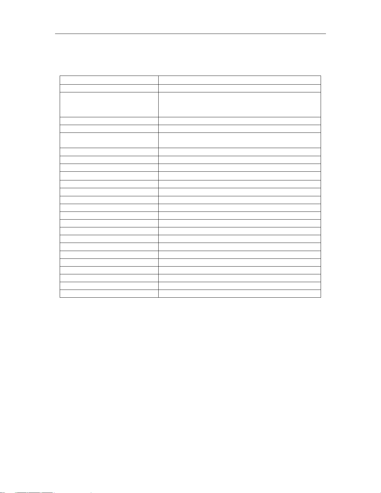
3.1 KG130 Block Diagram
Key Pad
24 Pin I/O Connector
①②③
①②③
④⑤⑥
④⑤⑥
⑦⑧⑨
⑦⑧⑨
ⓧⓞⓜ
ⓧⓞⓜ
32.768k XTAL
Backend IC
AIT701G
Spansion
128Mbit Nor
+ 64M SRAM
LCD(65K)
Main 1. 5”
300k Pixels
Camera
Memory Parallel
I nterface
Power
Serial Port
BB Chip
AD6720
Audio AMP
MAX9718
Vibrator
Speaker/RCV
Analog
Switch
(Including
830mAh
Li-Ion
PAM + FEM
(TQM6M4003)
Charging
Circuit
TRANSCEIVER
Othello G
(AD6548)
26MHz XTAL
Figure 3-1: KG130 Top Level Block Diagram
The Figure 3-1 shows the top level block diagram of KG130, it contains RF and BB part.
The following list is the detailed:
1. AD6720 : ADI baseband chipset,
including Digital Base Band (DBB) and Analog Base Band ABB
2.TQM6M4003: Triquint PAM and Ant Switch
3. Transceiver:ADI Othello G AD6548
4. Flash: Spansion 128Mbit + 64Mbit
5. Backend IC: AIT701G
6. Others:
A. 22 keys
B. 128 x 128 65K CSTN –LCD module
C. Vibrator
D. Mic
E. Speaker and receiver
F. Ear-jack
G. Sim socket
H. Battery connector
I. Camera connector and Camera Module
DBB and ABB)
Ear Mic
MIC
Circuit
SIM
SIM
MIC
6
3. TECHNICAL BRIEF
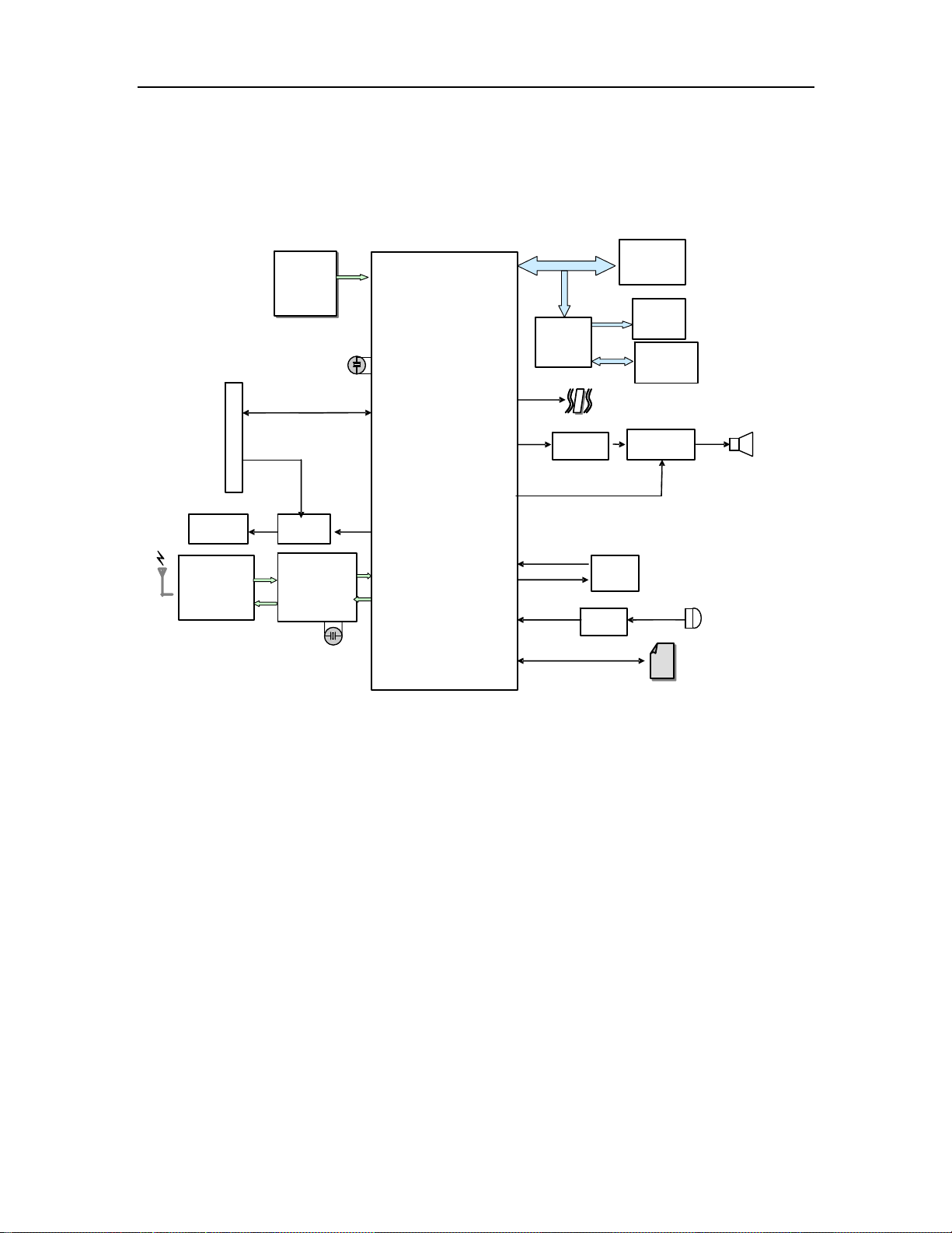
3.2 RF Part Introduction
The RF parts consists of a transmitter part, a receiver part, a voltage supply part, the
crystal reference system. And the main RF Chipset AD6548 is a highly integrated
direct conversion radio solution that combines, on a single chip, Quad Band Radio
( GSM850,E-GSM,DCS1800 and PCS1900 and power management functions
necessary to build the most compact GSM radio solution possible. This quad-band
GSM transmit module integrates a PA, a low-pass filter, a linear Tx / Rx switch along
with PA and switch control combined with ESD protection circuitry in one module,.
3.2.1 Receiver Part
The Receiver part in AD6548 contains all active circuits completely, full receiver chain
with the exception of discrete front-end RF SAW filters. The AD6548 uses direct
conversion receiver architecture of the OthelloTM family. For Quad band
applicationsthe front end features four fully integrated programmable gain differential
LNAs. The RF is then downconverted by quadrature mixers and then fed to the
baseband programmable-gain amplifiers and active filters for channel selection. The
Receiver output pins can be directly connected to the baseband analog processor. The
Receive path features automatic calibration and tracking to remove DC offsets. The RF
Receiver block is shown as below.
ANT
TXOP_HI
ANT
TXOP_LO
Vcc1
V1
(Internal Voltage)
TX RF Output
RX RF Input
ESD-
Diode
Vcc2
EGSM/GSM850 In
TX RF Input
Vmod_en
Vramp
Vbatt
Vtx
Vbs2
Vbs1
DCS/PCS In
TX RF Input
Logic
Power
Control
&
VCC_FE
RX850
RX850B
RX900
RX900B
SDATA
SCLK
SEN
RX1800
RX1800B
RX1900
RX1900B
LNA Gain Reduction
Generator
TX_LO
TX_LO1
2
Generator
Serial
Interface
/2
RX LO
TX LO
VCC_TXVC
O
Band
Control
TX circuits
Supply
LDO
Reg 3
TX Loop filter
PHD
Tx_LO1
DC Offset
Correction
DC Offset
Correction
Frac-N Synth VCTCXO
LO VCO
Supply
LDO
Reg 2
General
Supply
LDO
Reg 1
Supply
TXIB
TXI
I
IB
RX
I
/4
Tx_LO2
Ref
VCC_BBI
VCC_BBQ
Q
QB
RXQB
VAFC
AFC
REFINB
REFIN
REF_OP
REF_OP
VCC_REF
RXIB
TXQ
RX
CLK
TX
Q
B
A
B
S
E
Q
B
A
N
D
A.Low Noise Amplifiers
The AD6548 includes four fully integrated Low Noise Amplifiers (LNAs), to support
VDD
Figure 3-2: The RF Receiver Block
7

3. TECHNICAL BRIEF
quad band applications without further external active components. The LNAs have
differential inputs which minimize the effect of unwanted interferers. The inputs are
easily matched to industry standard FEMs or discrete Rx SAW filters. The outputs of
the LNAs are directly coupled to the down-converting mixers. The voltage gain of the
LNAs are typically 24 dB. Each LNA can be switch to a low gain mode when receiving
large input signals as part of the AGC system.
B.Down-Converting Mixers
Two quadrature mixers are used to mix down the signals from the LNAs, one for the
high bands (1800 and 1900 MHz) and one for the low bands (850 and 900 MHz). The
outputs of the mixers are connected to the baseband section through an integrated
single pole filter with nominal cut-off frequency of 800kHz. This acts as a “roofing filter”
for the largest blocking signals (i.e. those 3MHz) and prevents the baseband
amplifiers from being overloaded
.
C.Baseband Amplifiers / Low Pass Filters
The baseband amplifiers provide the majority of the analog receiver gain. The filtering
is provided by an integrated 5
th
order Chebyshev filter giving the necessary adjacent
channel and blocking filtering, it is also acting as an anti-alias filtering for Baseband
IC’s converters. A final low pass pole is possible at each of the baseband outputs via
internal series resistor along with an external shunt capacitor. The external capacitor is
not required with ADI baseband ICs. The on chip filter has an auto calibration feature
ensuring that the filters are tuned for optimum performance. The baseband amplifiers
have programmable gain for system AGC. A total of 57 dB of gain control is provided in
3dB steps programmable over the serial interface. This together with the LNA gain
control gives a total of 77dB of gain control range. The receive baseband outputs are
routed to the common Rx/Tx I/Q ports for connection with the baseband converters
D.Baseband Output D.C. Offset Correction
In order to minimize D.C. offsets inherent in the receiver and maximize dynamic range
a D.C offset correction circuit is integrated. This correction is triggered over the serial
bus and then an offset tracking loop is enabled to minimize residual offsets under all
conditions. The tracking loop is fully hardware integrated, requiring no software
intervention.
E.Receiver Local Oscillator (LO) Generator
The Rx LO generator is used to avoid DC offset problems associated with LO leakage
into the receiver RF path. By operating the VCO at a frequency other than the desired
receive frequencies,any leakage of the VCO (e.g. via package) will fall out of band. The
LO generator is used to convert the offset synthesized VCO output to the on-frequency
quadrature LO required by the chipset. The LO generator is implemented as a
regenerative frequency divider, performing a 2/3 multiplication of the VCO output for
the high band (DCS1800/PCS1900) and a 1/3 multiplication for low band
(E-GSM/GSM850).
.
3.2.2 Transmitter Part
The Transmitter part contains AD6548 active parts and PAM .The transmit section of the
AD6548 radio implements a translation loop modulator. This consists of a quadrature
modulator, high speed phase-frequency detector (PFD) with charge
filter, TX VCO and a feedback down converting mixer. The VCO output (divided by 2
for low band) is fed to the power amplifier with a portion internally fed back
pump output, loop
into the
8
3. TECHNICAL BRIEF
down-converting feedback mixer to close the feedback loop.
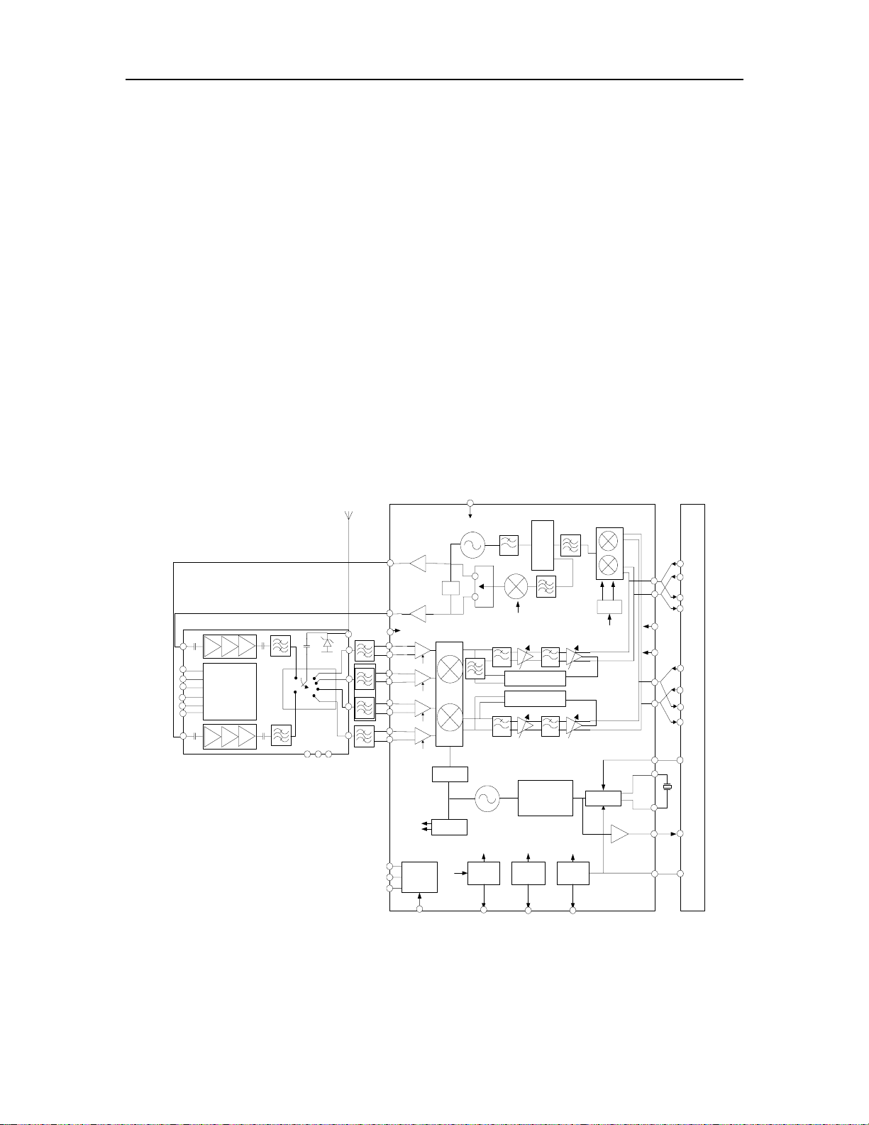
A. Power Amplifier Module
EGSM/GSM850 In
Vmod_en
Vramp
Vbatt
Vtx
Vbs2
Vbs1
DCS/PCS In
TX RF Input
The advanced quad-band Transmit Module designed for mobile handset applications
provides full RF transmit functionality.The GSM850/900 and DCS/PCS power amplifier
blocks including power control are combined with the low insertion loss quad-band
pHEMT switch, Tx harmonics filtering, integrated switch decoder, four receive ports,
and full ESD protection. This architecture eliminates the need for any PA-to-switch
design effort for phone designers. All four Rx ports are frequency independent and
allow flexible routing to the transceiver. Fabricated in high-reliability InGaP HBT /
pHEMT technology, the module supports GPRS class 12 operation and provides 50
Ohms input and output impedances at all RF input and output ports. The module
control inputs are CMOS compatible and has no need for an external reference voltage.
With its excellent efficiency performance in all 4 bands, the power amplifier and switch
module contributes to the overall talktime targets of next generation mobile handset
designs.
Operating
Mode
TX GSM 850/900
TX DCS/PCS
RX1
RX2
RX3
RX4
Sleep Mode
Vmod_en Vtx Vbs1 Vbs2
ANT
TX RF Output
TX RF Input
Logic
&
Power
Control
V1
RX RF Input
ESD-
Diode
Vcc1
Vcc2
(Internal Voltage)
Figure 3-3: Power Amplifier Module
Control Voltage
H H L L
H H H L
H L L L
H L L H
H L H L
H L H H
L L L L
Table 3-1: PAM Truth Table
B.Quadrature Modulator
The Quadrature modulator takes the baseband I & Q signals and translates these into
a GMSK signal at the Transmit Intermediate Frequency (TX IF). After bandpass filtering
and limiting the TX IF signal is used as the reference input to the Phase Frequency
Detector (PFD) of the transmit PLL.
9

3. TECHNICAL BRIEF
C.Phase Frequency Detector (PFD)
The PFD ensures that the transmitted signal contains the required modulation and is
accurately locked to the desired GSM channel. The downconverted feedback signal
from the TXVCO and the Quadrature Modulator output are phase compared by the
PFD. The PFD charge pump generates a current pulse proportional to the difference in
phase which is applied to the loop filter.
D.Loop filter
To minimize complexity of the external PCB layout the TX loop filter is fully integrated
into the IC. At power up the filter is automatically calibrated as part of the baseband
filter cal, eliminating process tolerances. The calibration is fully integrated and requires
no extra programming.
E.TX VCO
The Transmit Voltage Controlled Oscillator (TX VCO) and tank components are a fully
integrated subsystem. The subsystem includes PA drivers so the outputs are used to
directly drive the external PAs. The low noise oscillator design and internal filtering
mean that external TX SAW filters are not required. In Low band operation the TX VCO
output is divided by two and filtered. The TX VCO is automatically calibrated to ensure
optimum performance over its operating frequency of 1648 to 1910 MHz.
F.Feedback Down-Converting Mixer
The feedback down converting mixer is used to translate the TX VCO output frequency
to the TX IF. An integrated band pass filter exists between the mixer and the PFD to
filter the mixers unwanted side band and higher order mixing products.
G.Transmit Frequency Plan
Unlike many other translation loop modulators the AD6548 uses only a single VCO
source to derive the local oscillator signal for both the Feedback Down-Converting
Mixer and the Quadrature modulator. Therefore there is a fixed relationship between
the Tx IF frequency and the LO VCO frequency .This ratio was chosen to minimize
VCO tuning range, TX IF frequency variation and ensure excellent transmit spectral
mask performance. The Feedback-Down Converting Mixer operates low side injection
for the high bands and high side injection for the low bands. The final relationship
between the transmitted TX frequency frequency and the LO VCO frequency is
different between the two bands. These relationships are taken account of in the
synthesizer architecture and programming.
H.Main Frequency Synthesizer
The AD6548/9 has a single fast-locking fractional synthesizer used for VCO control in
both receive and transmit mode. The entire system including VCO, tank, fractional N
dividers, sigma delta compensation, charge pump and loop filters are fully integrated.
The only external component is a low cost crystal for the reference. The synthesizer is
controlled via the serial interface. The VCO is fed into the respective dividers to
generate the appropriate LO frequencies for the RX and TX bands.
I.Fractional N Dividers
The fractional N divider allows the PLL system to have a smaller step size than the
comparison frequency which is set by the external reference to 26 MHz. This feature
allows all the GSM frequency band rasters to be achieved, with fast lock times and
good phase noise characteristics. The divider section consists of a dual modulus 8/9
prescaler, integer M & A dividers, and fractional N system based on sigma-delta
modulation to generate the required fractional divide ratio. The Denominator of the
10
3. TECHNICAL BRIEF
fractional divider can be set to 3 different values, (1040, 1170, 1235), depending on the
mode of operation. For example a denominator of 1040 with an input fraction F
maintains an average value of F/1040 allowing 25 kHz steps when operated at a
reference of 26 MHz.
J.Phase Frequency Detector/Charge Pump
A Phase Frequency Detector (PFD) is used for the PLL phase detector. The charge
pump is designed such that good matching of up and down currents is achieved over a
wide output operating range. The charge pump output is internally routed to the
integrated synthesizer loop filter.
K.Synthesizer Loop filter
To minimize complexity of the external PCB layout the Main Synthesizer loop filter is
also fully integrated into the IC. No external components or adjustments are required .
L.Voltage Controlled Oscillator
The integrated voltage controlled oscillator (VCO) is a complete self-calibrating
subsystem. This employs a fully automated digital self-calibration function to ensure
optimum phase noise performance over the entire frequency range. The VCO
generates frequencies between 2520MHz and 2985MHz as required to operate in the
four bands for RX and TX.
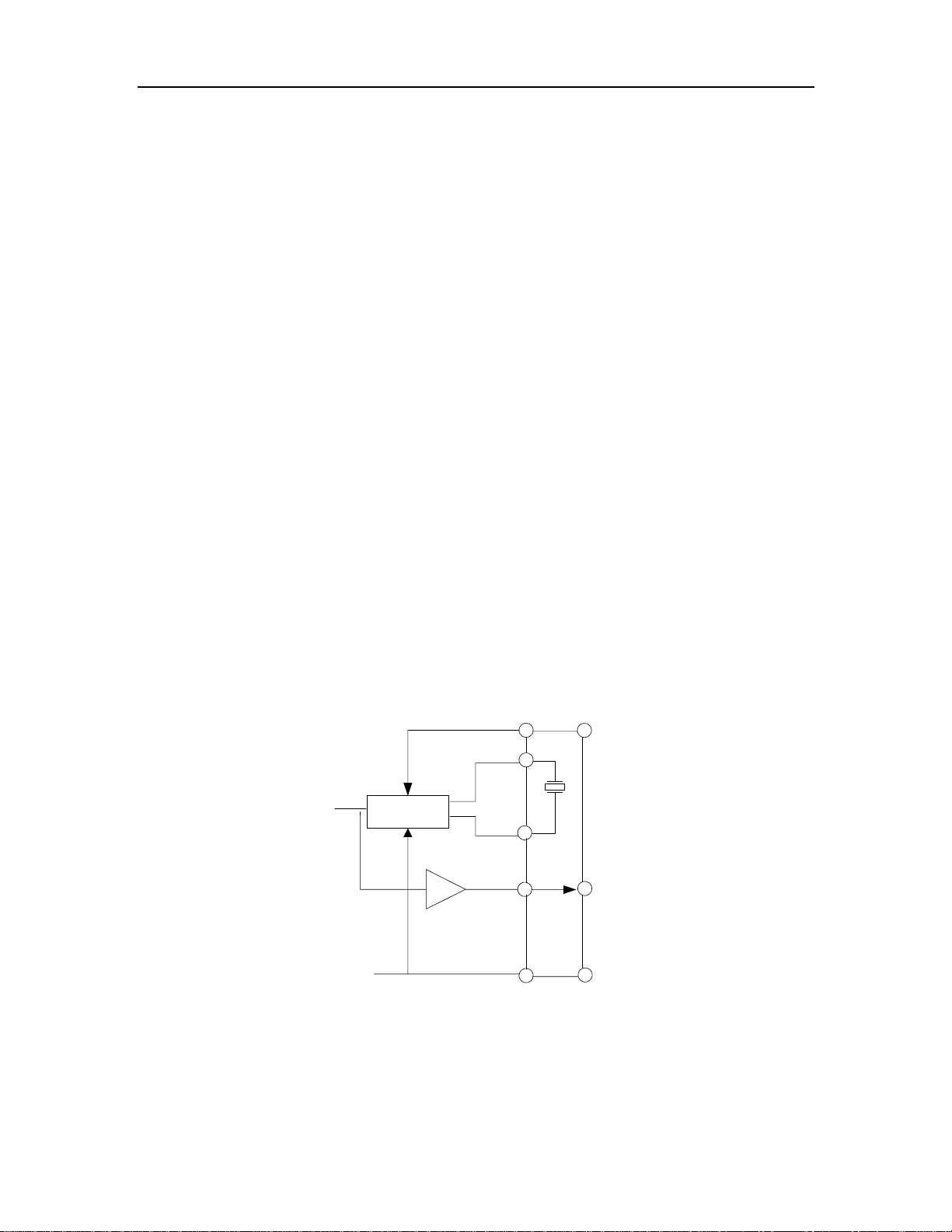
3.2.3 The Crystal Reference System
The AD6548 requires only an external low cost crystal as the frequency reference. The
circuitry to oscillate the crystal and tune its frequency is fully integrated. The Oscillator
is a balanced implementation requiring the crystal to be connected across 2 pins.
There is a programmable capacitor array included for coarse tuning of fixed offsets (e.g.
crystal manufacturing tolerance), and an integrated varactor for dynamic control. The
oscillator is designed for use with a 26MHz crystal. The crystal is connected as shown
in figure.
VAFC
AFC
REFINB
VCTCXO
Supply
Ref
REFIN
REF_OP
CLK
REF_OP
VCC_REF
Figure 3-4: The Crystal Reference System
Dedicated control software ensures excellent frequency stability under all
circumstances.
11
3. TECHNICAL BRIEF
3.2.4 Power Management
For direct battery supply connect, and to reduce external circuitry complexity the
AD6548/9 features three Low Drop Out Regulators (LDOs). The three LDOs provide
isolation of the oscillators and sensitive circuits from unwanted power supply and cross
coupled noise. They also ensure the IC operation is robust over a wide range of power
supply voltages. For power management the LDOs are independently controlled via
the 3 wire serial bus.
A.LDO Usage
The following table describes the LDO usage:
LDO1 LDO2 LDO3
Rx and Tx baseband
sections
Table 3-2: Intended LDO Use
The LDO outputs require external connection to the respective pins described in table
3, and each requires decoupling capacitors.The LDOs are designed to be
unconditionally stable regardless of the capacitor’s ESR.
LDO OP External Connection
VLDO1 VCC_FE, VCC_BBI, VCC_BBQ
VLDO2 No external Connections, except for decoupling
VLDO3 No external Connections, except for decoupling
Table 3-3: LDO Connections
Main VCO TX VCO
LDO1 derives its input references from the crystal supply voltage (VCC_REF). It is
therefore expected that VCC_REF be supplied from a external LDO of nominal supply
voltage 2.75V
(e.g. ADP3330 or Analog Baseband IC: Vout=2.75V1.4%)
3.3 Baseband Introduction
3.3.1 Baseband Processor (AD6720 , U101)
• AD6720 is an ADI designed processor
• AD6720 consists of
1. Control Processor Subsystem including:
• 32-bit MCU ARM7TDMI Control Processor
• 39 MHz operation at 1.8V
• 1Mb of on-chip System SRAM Memory
2.DSP Subsystem including:
• 16-bit Fixed Point DSP Processor
• 91 MIPS at 1.8V
• Data and Program SRAM
• Program Instruction Cache
• Full Rate, Enhanced Full Rate and Half Rate
• Speech Encoding/Decoding
• Capable of Supporting AMR & PDC Speech Algorithms
3.Peripheral Functions
• Parallel and Serial Display Interface
• Keypad Interface
• Flash Memory Interface
• Page-Mode Flash Support
12
3. TECHNICAL BRIEF
• 1.8V and 3.0V, 64 kbps SIM Interface
• Universal System Connector Interface
• Data Services Interface
• Battery Interface (e.g. Dallas)
4. Other
• Supports 13 MHz and 26 MHz Input Clocks
• 1.8V Typical Core Operating Voltages
• 289-Ball Package (12x12mm) , 0.65mm Ball pitch
5. The AD6720 baseband transmit section supports the following
• mobile station GMSK modulation power classes:
• GSM 900/850 power classes 4 and 5,
• DCS 1800 power classes 1 and 2, and
• PCS 1900 power classes 1 and 2
3.3.2 Interconnection with external devices
A. RTC block interface
Countered by external X-TAL
The X-TAL oscillates 32.768KHz
B. LCD module interface
Signals Description
L_LCD_CS MAIN LCD driver chip enable.
_LCD_RESET This pin resets LCD module.
L_WR Enable writing to LCD Driver.
L_RD Enable reading to LCD Driver.
L_RS This pin determines whether the data to LCD module data or control data.
A1 Select 16bits interface mode for MAIN LCD.
Table 3-4: LCD Pin Description
The backlight of LCD module is controlled by AD6720 via AAT3110 , U303. The control
signals related to Backlight LED are given bellow.
Signals Description
LCD_LED_CTL Control LCD backlight level in 4 steps
DISP_LIGHT Current source for backlight LED
Table 3-5. Description Of LCD Backlight LED Control
C. RF interface
The AD6720 control RF parts through ANT_SW1, ANT_SW2, PA_EN, S_EN, S_DATA,
S_CLK.
13
3. TECHNICAL BRIEF
Signals Description
ANT_SW1 (GPO9)Antenna switch Band Select
ANT_SW2 (GPO8)Antenna switch Band Select
PA_EN (GPO16) PAM Enable/Disable
S_EN (GPO19) PLL Enable/Disable
S_DATA (GPO20) Serial Data to PLL
S_CLK (GPO21) Clock to PLL
Table 3-6. RF Control Signals Description
D. SIM interface
The AD6720 provides SIM Interface Module. The AD6720 checks status periodically
during established call mode whether SIM card is inserted or not, but it doesn't check
during deep Sleep mode. In order to communicate with SIM card, 3 signals SIM_DATA,
SIM_CLK, SIM_RST(GPIO_23) are required. The descriptions about the signals are
given by bellow Table 3-7 in detail.
Signals Description
SIM_DATA This pin receives and sends data to SIM card. This model can support only3.0
volt interface SIM card.
SIM_CLK Clock 3.25MHz frequency.
SIM_RST Reset SIM block(GPIO_23)
Table 3-7: SIM Control Signals Description
SIM CONNECTOR
SIMDATAOP
2V85_VSIM
R333
20K
C327
NA
J300
SCK-6S-12PT-TF
5
GND
6
VPP
7
IO
VCC
RST
CLK
2V85_VSIM
1
2
3
C330 220n
C326
2.2u
(1608)
SIMRESET
SIMCLK
R335 0
C332 1000p
C331 NA
Figure 3-5: SIM Interface of AD6720
14

3. TECHNICAL BRIEF
E. LDO Block
There are 8 LDOs in the AD6720.
- VCORE : supplies Digital base band Processor core and AD6720 digital core
- VMEM : supplies external memory and the interface to the external memory on the
digital base band processor (1,8V or 2.8V, 150mA)
- VEXT : supplies Radio digital interface and high voltage interface (2.8V, 170mA)
- VSIM : supplies the SIM interface circuitry on the digital processor and SIM card
(2.85V, 20mA)
- VRTC : supplies the Real-Time Clock module (1.8 V, 20μA)
- VABB : supplies the analog portions of the AD6720
- VMIC : supplies the microphone interface circuitry (2.5 V, 1 mA)
- VVCXO : supplies the voltage controlled crystal oscillator ( 2.75 V, 10 mA)
3.3.3 Battery Charging Block
1. It can be used to charge Lithium Ion batteries.
Charger initialization, trickle charging, and Li-Ion charging control are implemented in
hardware.
2. Charging Process
- Check charger is inserted or not
- If AD6720 detects that Charger is inserted, the CC-CV charging starts.
- Exception : When battery voltage is lower than 3.2V, the precharge(low current
charge mode)
starts firstly.
- And the battery voltage reach to 3.2V the CC-CV charging starts.
3. Pins used for charging
- VCHG : charger supply.
- GATEDRIVE : charge DAC output
- ISENSE : charge current sense input
- VBATSENSE : battery voltage sense input.
- BATTYPE : battery type identification input
- REFCHG : voltage reference output
4. TA (Travel Adaptor)
- Input voltage: AC 85V ~ 260V, 50~60Hz
- Output voltage: DC 5.2V ( 0.2 V )
- Output current: Max 800mA ( 50mA )
5. Battery
- Li-ion battery (Max 4.2V, Nom 3.7V)
- Standard battery: Capacity - 830mAh
15

3. TECHNICAL BRIEF
PRECHARGE
VCHARGE VBAT
PRE_C HARGE
VCHARGE
R343 20K
VBAT
R345
100K
C333
1u
R338
15
3
2 5
1 6
Q301
UMX1NTN
R340
1K
4
C130
4.7u
D103
CUS02
R112 330
5
S
6
D4
7
D5
8
D6
Q100
TPCF8102-TE85L-F
C131
1u
D3
D2
D1
G
R107
0.2
(1%)
C12
VCHG
A12
GATEDRI VE
C13
ISENSE
B13
VBATSENSE
C129
0.1u
F17
B12
REFCHG
BATTY PE
R110 82K
4
3
2
1
BA TT_TEMP
(1%)
Figure 3-6: Circuit For Battery Charging
16
3. TECHNICAL BRIEF
3.3.4 Display and Interface
• Main LCD
Controlled by L_ LCD_CS, _LCD_RESET, L_RS, L_WR, L_RD, LCD_ID,
L_DATA[00:15] ports
• L_ LCD_CS : MAIN LCD driver chip enable. MAIN LCD driver IC has own CS pin
• LCD_RST : This pin resets LCD module. This signal comes from AD6720 directly.
• _L_RESET: This pin determines whether the data to LCD module are display data or
control data.
• L_WR : Write control Signal
• L_RD : Read control Signal. But this pin used only for debugging.
• L_DATA[00:15] : Parallel data lines.
• LCD_ID: LCD type selection signals
• For using 65K color, data buses should be 16 bits.
Properties Spec. Unit
Active Screen Size 35.78*40.05*2.8 mm
Color Depth 65,536 colors
Resolution 128 X RGB X 128 dots
FL302
EVRC18S05Q030100R
_LCD_R ESET
L_DATA00
L_DATA01
L_DATA02
L_DATA03
L_DATA04
L_DATA05
L_DATA06
L_DATA07
L_RS
L_LCD_CS
L_WR
L_DATA08
L_DATA09
L_DATA10
L_DATA11
L_DATA12
L_DATA13
L_DATA14
L_DATA15
9
INPU T_B1
8
INPU T_B2
7
INPU T_B3
6
INPU T_B4
10
FL307
EVRC18S05Q030100R
9
INPU T_B1
8
INPU T_B2
7
INPU T_B3
6
INPU T_B4
10
FL309
EVRC18S05Q030100R
9
INPU T_B1
8
INPU T_B2
7
INPU T_B3
6
INPU T_B4
10
1
INPU T_A1
2
INPU T_A2
3
INPU T_A3
4
INPU T_A4
G15G2
1
INPU T_A1
2
INPU T_A2
3
INPU T_A3
4
INPU T_A4
G15G2
1
INPU T_A1
2
INPU T_A2
3
INPU T_A3
4
INPU T_A4
G15G2
Figure 3-7: LCD Interface Circuit
FL306
EVRC18S05Q0 30100R
9
INPU T_B1
8
INPU T_B2
7
INPU T_B3
6
INPU T_B4
10
FL308
EVRC18S05Q 030100R
9
INPU T_B1
8
INPU T_B2
7
INPU T_B3
6
INPU T_B4
10
INPU T_A1
INPU T_A2
INPU T_A3
INPU T_A4
G15G2
INPU T_A1
INPU T_A2
INPU T_A3
INPU T_A4
G15G2
LCD CONN ECTER
2V8_VMEM
C328 1u
1
2
3
4
LCD_LED_CTL
1
2
3
4
LIGHT2
LIGHT1
R341
R342
L_RD
LCD_I D
56
56
C329 1u
R344
NA
R346 51K
2V8_VMEM
R337
51K
10
11
12
13
14
15
16
17
18
19
20
21
22
23
24
25
26
27
28
29
30
31
32
33
34
35
36
37
38
39
40
41
CN302
1
2
3
4
5
6
7
8
9
17
3. TECHNICAL BRIEF
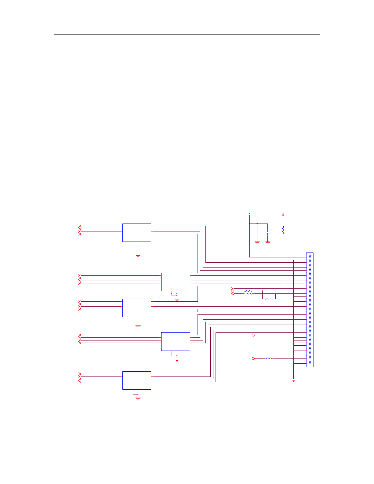
3.3.5 Keypad Switches and Scanning
The key switches are metal domes, which make contact between two concentric pads
on the keypad layer of the PCB when pressed. There are 22 switches, connected in a
matrix of 5 rows by 5 columns, as shown in Figure 3-x, except for the power switch
(KB1), which is connected independently. Functions, the row and column lines of the
keypad are connected to ports of AD6720. The columns are outputs, while the rows are
inputs and have pull-up resistors built in. When a key is pressed, the corresponding
row and column are connected together, causing the row input to go low and generate
an interrupt. The columns/rows are then scanned by AD6720 to identify the pressed
key.
SW222
POWER
VBAT
R201
10K
R202 680
R203
NA
KEYON
KEYPAD
SW201
RIGHT
SW205
3
SW209
6
SW213
9
SW217
#
SW202
UP
SW206
2
SW210
5
SW214
8
SW218
0
SW203
LEFT
SW207
1
SW211
4
SW215
7
SW219
*
SW204
DOWN
SW208
MEN U
SW212
OK
SW216
SEND
SW220
SELECT
SW221
CLR
NA
R209
NA
R210
NA
R211
NA
R212
NA
R213
R214 NA
R215 NA
R216 NA
R217 NA
R218 NA
R204 680
R205 680
R206 680
R207 680
R208 680
Figure 3-8: Keypad Switches and Scanning
KEY_R OW0
KEY_R OW1
KEY_R OW2
KEY_R OW3
KEY_R OW4
KEY_C OL4
KEY_C OL3
KEY_C OL2
KEY_C OL1
KEY_C OL0
18
3. TECHNICAL BRIEF
3.3.6 Microphone
The microphone is placed to the front cover and contacted to main PCB. The audio
signal is passed to AIN1P and AININ pins of AD6720. The voltage supply VMIC is
output from AD6720, and is a biased voltage for the AIN1P. The AIN1P and AIN1N
signals are then A/D converted by the voiceband ADC part of AD6720.The digitized
speech (PCM 8KHz ,16KHz) is then passed to the DSP section of AD6720 for
processing (coding, interleaving etc).
2V5_VMIC
R243
1K
C229
39P
C232
39P
VINN ORP
VINNORN
C227
39P
R245
100
R247
100
R244
2.2K
R246
0
C228
0.1u
R249
2.2K
Figure 3-9: Connection Between Microphone And AD6720
3.3.7 Soft-midi and Main Speaker
The TTPCom Embedded MIDI & Polyphonic Orchestra product, “TEMPO”, is a
complete MIDI music player solution offering the following features:
• MIDI-standards compliant
• MIDI files playable as polyphonic ringtones
• Low memory footprint - less than 8 kB internal MCU system RAM
• 40 notes polyphony
• Intelligent note-stealing algorithm ensures optimum use of available synthesiser
polyphony
• Open API enabling product differentiation via the addition of MIDI music support
to existing and new customer applications
• MIDI file parser supports Standard MIDI (formats 0, 1 and 2), SMAF-MA3, GM-Lite
and SP-MIDI
The main speaker is driven directly by AD6720 AOUT1P and AOUT1N pins and the
gain is controlled by the PGA in an AD6720.
CLOSE TO MIC
+
C230
10U
C231
39P
C233
39P
VA201
EVL5M02200
MIC 200
OB4-15L42-C33L
VA202
EVL5M02200
19
3. TECHNICAL BRIEF
VBAT
SPK_P
SPK_N
C221 0.1u
C222 0.1u
C243
0.1u
R275 10K
R276 10K
C223
1u
C217
0.1u
R238 10K
U202
MAX9716ETA+T
VCC6_SHDN
2
BIAS
3
IN+
4
IN-
R239 10K
C244 0.1u
C218
4.7u
(1608)
OUT-
OUT+
GND
PGND
1
8
5
7
9
AUDIO
AMP_SHDN
RCV_P
RCV_N
R250
100K
VBAT
C220
1u
U203
MAX4684EBC_T
B4
C4
NO1
A4
NO2
C1
NC1
A1
NC2
C2
IN1
V+
A2
IN2
C3
COM1
A3
COM2
GND
B1
C219
NA
(1608)
SPK_RCV_SEL
HIGH
LOW
R240 0
R241 0
R242
(FOR TUNING NOISE)
10K
SELECT
SPEAK ER
RECEIVER
SPK_RCV_SEL
SPK_RCV_P
SPK_RCV_N
SPK_RCV_P
SPK_RCV_N
C224
39p
C240
VA206
VA207
EVLC5S0250
EVLC5S0250
C241
39p
39p
SP201
SP202
RC201
RC202
Figure 3-10: Main Speaker Circuit
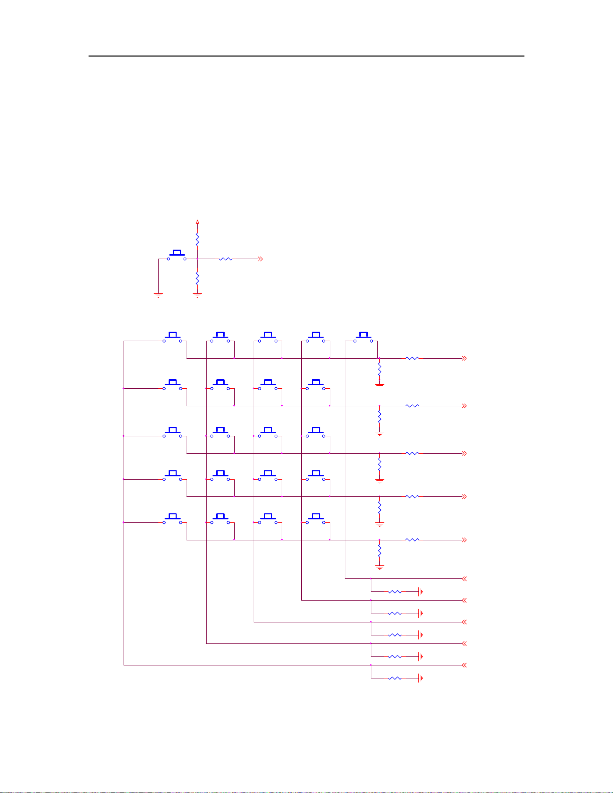
3.3.8 Headset Interface
This phone has 5 electrodes such as GND, AUXIP, ACK_DETECT, HOOK_DETECT.
This type supports mono sound.
Switching from Receiver to Headset Jack
If jack is inserted, JACK_DETECT goes from high to low.
Audio path is switched from receiver to earphone by JACK_DETECT interrupt.
Switching from Headset Jack to Receiver
If jack is removed, JACK_DETECT goes from low to high.
Audio path is switched from earphone to receiver by JACK_DETECT interrupt.
Hook detection
If hook-button is pressed, HOOK_DETECT is changed from low to high.
This is detected by AUXADC2.
And then hook is detected.
20
3. TECHNICAL BRIEF
2V5_JACK
+
C208
10u
2V5_JACK
C216
1u
R226
1.5K
C209
NA
C211 0.1u
JACK_D ETECT
HEADSET_MIC_N
R230 0
C215
C226
NA
2V8_VEXT
1u
C207 0.1u R225 20K
C210
39P
1
U205
LMV7291MGX-N OPB
R248 100K
2V8_VEXT 2V8_VEXT
R229
1M
HEADSET_SPK_P
3
+
VCC
-
GND
2 5
HEADSET_MIC_P
4
R231
330K
U201
MIC5255-2.5UYM5
5
2
OUT
IN
3
GND
4
BYPEN
C242
0.01u
Figure 3-11: Headset Jack Interface
3.3.9 Key Back-light Illumination
In key back-light illumination, there are 6 Blue LEDs in Main Board, which are driven by
KEY_BACKLIGHT signal from AD6720.
KEY BACKLIGHT
EAR JACK
R227
330
C225
39p
C212 10u R234 4.7
R232 0
R233 4.7
C213
39P
VA205
EVL5M02200
HOOK_DETECT
R244 1M
J200
5
1
3
4
2
VA205
EVL5M02200
VA203
C214 39P
EVL5M02200
(6 LIGH T)
VBAT
47
R219
LD201
LEBB-S14H
47
C201 1u
R220
LD202
LEBB-S14H
47
C202 1u
R221
LD203
LEBB-S14H
47
C203 1u
LD204
LEBB-S14H
C204 1u
R222
LD205
Figure 3-12: Key Backlight Illumination
3.3.10 LCD Back-light Illumination
LCD backlight LEDs is controlled by AD6720 via AAT3110, U303.
47
R223
LEBB-S14H
47
C205 1u
LD206
LEBB-S14H
C206 1u
R224
KEYBOAR D_BACKLIGHT
21
3. TECHNICAL BRIEF
CH AR GE PUMP
VBAT
C317
10u
C316
1u
3.3.11 VIBRATOR
The vibrator is placed in the folder cover and contacted to LCD MODULE. The vibrator
is driven from VIBRATOR (GPIO_0) of AD6720
U303
AAT3110IGU-5_T1
6
5
4
C+
VIN
C-
VOUT
GND
_SHDN
1
2
3
FB301
C312
10u
R330 10
R331
NA
Figure 3-13: Main LCD Backlight Illumination
VIBRATOR
VBAT
R329
0
LCD_LED_CTL
DISP_LIGHT
VIB301
D300
VIBRATOR
C323 100p
R334
C324 1000p
C325 0.1u
1.5K
R336
100K
1SS352-TPH3_F
3
2
1
VIB302
C320 1u
R332
12
Q302
2SC5585
Figure 3-14: Vibrator Circuit
22
3. TECHNICAL BRIEF
3.3.12 CAMERA
The AIT701G is a highly integrated versatile multi-media processor for image-enabled
mobile and handheld devices, such as cellular phones and PDAs. The AIT701G
includes an 8-bit micro-controller, frame/display memory, high-quality image processor,
real-time JPEG CODEC, video processor, 2D-Graphic Engine and LCD Display
Interface.
The on-chip image processor implements the most advanced algorithm to deliver
professional-grade image quality, which also supports versatile features of digital still
camera like AE(Auto Exposure), AWB(Auto White Balance), Digital Zoom and a variety
of image special effects. The maximum resolution supported by AIT701G is
300K–pixel.
The on-chip JPEG CODEC is compliant with the JPEG baseline standard (ISO/IEC
10918) and JFIF formats, which performs real-time compression and decompression
at the rate of 30 frame per second with VGA resolution. The image size could be
dynamically adjusted by easily programming the internal registers.
The LCD Display Interface of AIT701G supports dual displays that can be TFT, TFD,
LTPS, or Color-STN LCD panels. The AIT701G could support a wide range of
resolutions of LCD panels up to 128*160.
Figure 3-15: Application Block Diagram
23
3. TECHNICAL BRIEF
CAM_WAIT
2V8_VCAM
CAM_HOLD
2V8_VCAM
R328
10K
13MHz_AIT
C318
1u
DATA00
DATA01
DATA02
DATA03
DATA04
DATA05
DATA06
DATA07
DATA08
DATA09
DATA10
DATA11
DATA12
DATA13
DATA14
DATA15
_LCD_CS
_RD
_WR
ADD16
ADD01
CAM_RST
C_RST
C311
39p
Figure 3-16: Chip block diagram
U301
E10
K10
H10
G10
F10
J10
H5
H6
D3
J3
H3
K4
J4
K5
J5
K6
J6
J9
H9
G9
G8
K7
K1
J1
K2
J7
J8
K3
K8
F2
K9
J2
G3
H4
AIT701G
VDD_CORE
GND_CORE
PSCAN_EN
PTEST_EN
PHD0
PHD1
PHD2
PHD3
PHD4
PHD5
PHD6
PHD7
PHD8
PHD9
PHD10
PHD11
PHD12
PHD13
PHD14
PHD15
PHLCD _BY
PHCS_
PHRD _
PHWE_
PHLCD _A0
PHIN T
PRST_
PHLCD 2_C S_
PHGPIO_CS_
PS_RST_
PHWAI T_
PMCLK
VDD_I O0
GND_IO0
PGPIO0
PGPIO1
PGPIO2
PGPIO3
PGPIO4
PGPIO5
PGPIO6
PGPIO7
PLCD0
PLCD1
PLCD2
PLCD3
PLCD4
PLCD5
PLCD6
PLCD7
PLCD8
PLCD9
PLCD1 0
PLCD1 1
PLCD1 2
PLCD1 3
PLCD1 4
PLCD1 5
PLCD1 6
PLCD1 7
GND_I O2
VDD_I O2
PLCD2_CS_
PLCD1_CS_
PLCD_RD_
PLCD_A0
PLCD_WE_
PHSY NC
PVSYN C
PSEN
PSDA
PSCK
PDCLK
PPXL_C LK
VDD_I O1
GND_I O1
1V8_VCAM
C301
0.01u
R349 0
R348 NA
R327
10K
R350 NA
C315 1000p
C319
1000p
Figure 3-17: CIRCUIT DIAGRAM
PD0
PD1
PD2
PD3
PD4
PD5
PD6
PD7
E9
D9
C10
B9
A7
B7
F9
D10
A10
B10
A9
C9
D8
A8
B8
C8
C7
C6
B6
C5
B5
A6
C4
A5
B4
C3
F8
E8
A2
B2
A3
B3
A4
E3
G1
E2
E1
D1
D2
C2
C1
A1
B1
H1
H2
G2
F3
F1
H8
H7
PSEN
HIGH
LOW
L_DATA00
L_DATA01
L_DATA02
L_DATA03
L_DATA04
L_DATA05
L_DATA06
L_DATA07
L_DATA08
L_DATA09
L_DATA10
L_DATA11
L_DATA12
L_DATA13
L_DATA14
L_DATA15
L_LCD_CS
L_RD
L_RS
L_WR
C_HS
C_VS
C_CD00
C_CD01
C_CD02
C_CD03
C_CD04
C_CD05
C_CD06
C_CD07
C_ENABLE
C_SDA
C_SCK
C_MCLK
C_PCLK
SENSOR STATUS
DEACTIVE
AC TI VE
2V8_VCAM
C305
1u
2V8_VCAM
C321
1u
24
4. Trouble shooting
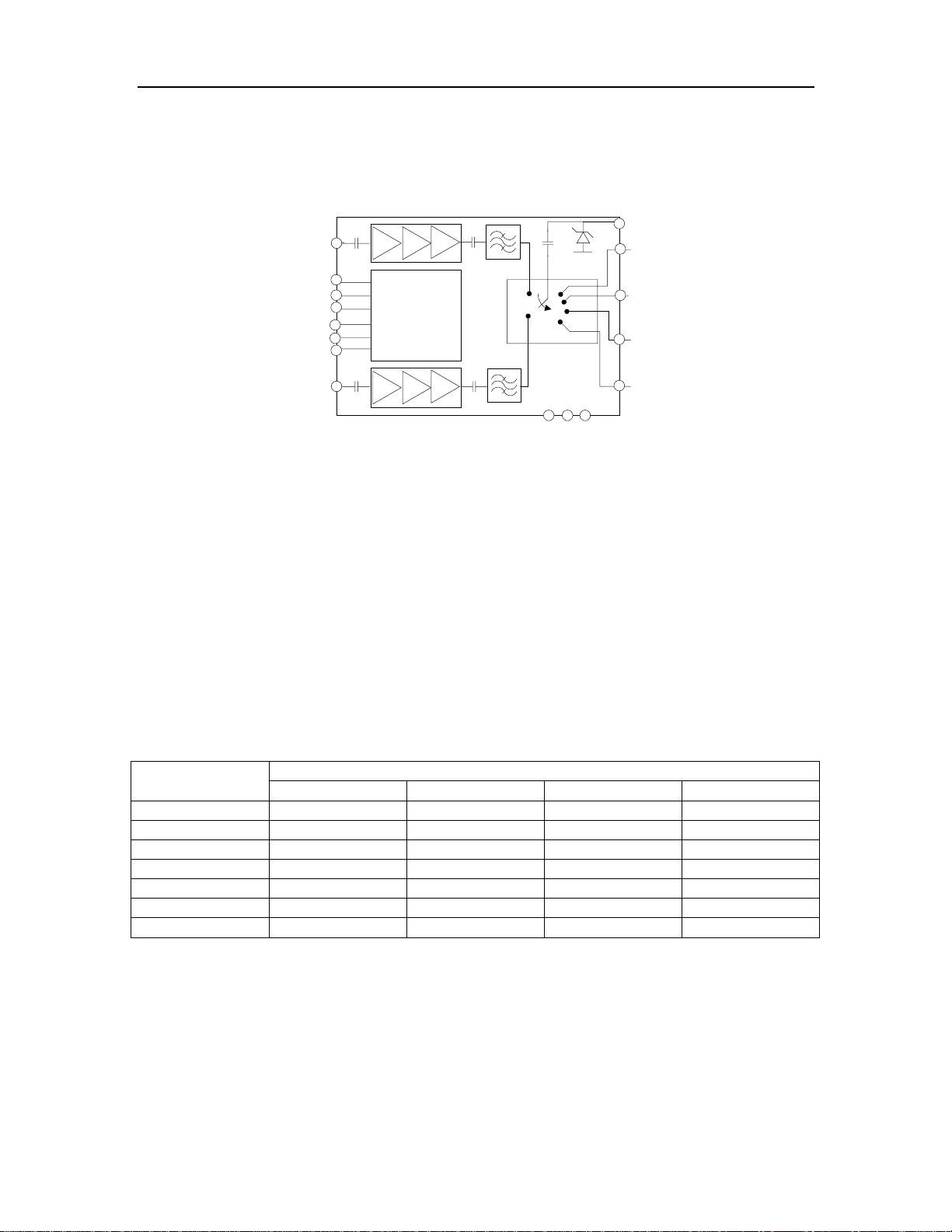
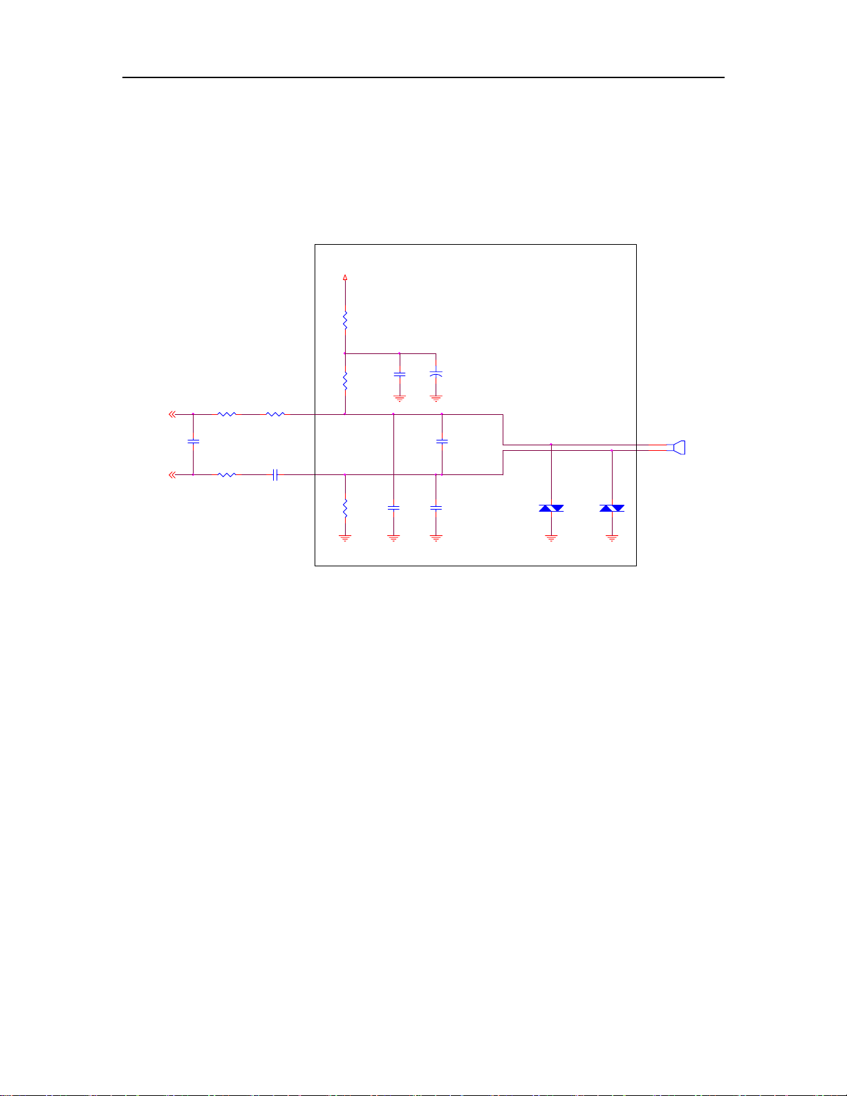
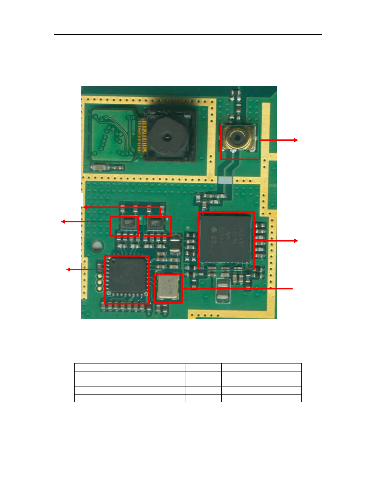
4.1 RF components
4. TROUBLE SHOOTING
SW400
FL402
FL400
U402
U401
X400
Figure 4-1
Table 4-1
Reference Description Reference Description
U401 Power Amplifier module FL400 SAW filter GSM&DCS
U402 Transceiver IC chip FL402 SAW filter PCS&GSM850
X400 Crystal
SW400 Mobile Switch Module
25
4. TROUBLE SHOOTING
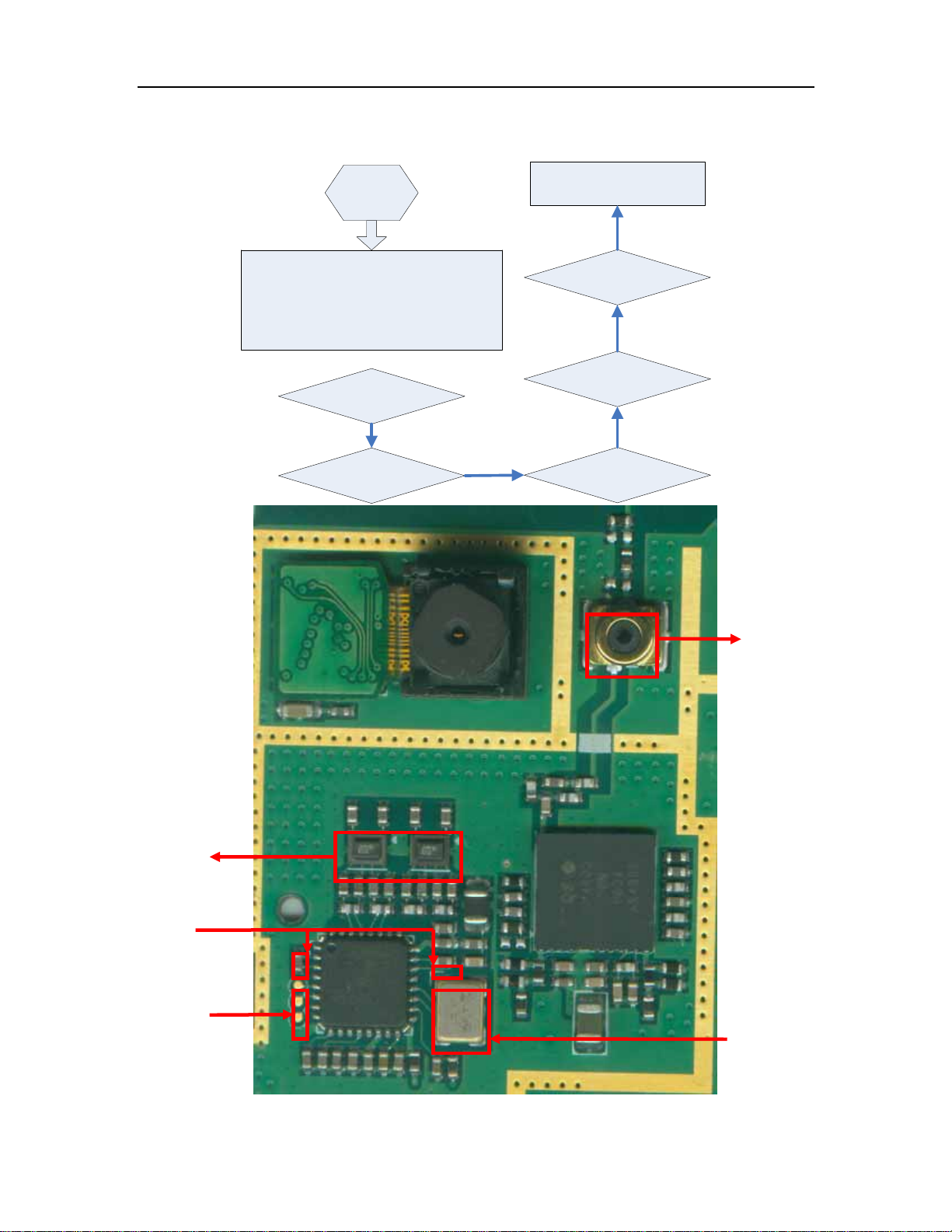
4.2 RX Trouble
Start
HP8960: test mode
62CH,7 level setting (TCH)
62CH,-60dBm setting (BCCH)
Spectrum Analyzer setting
Oscilloscope setting
1. Check crystal circuit
2. Check Control Signal
Redowload SW, CAL
5. Check RX I/Q Signal
4. Check SAW
Filter circuit
3. Check Mobile SW
& ANT SW
3
4
5
2
1
Figure 4-2
26
 Loading...