

LG K430DSF Service Manual
Date:Feb 2016 / Ver. 1.0
BEFORE SERVICING THE UNIT, READ THE “SAFETY PRECAUTIONS” IN THIS MANUAL
MOBILE PHONE
SERVICE MANUAL
CAUTION
MODEL : LG-K430DSF

T a b l e Of Contents
2
Copyright ⓒ 2016 LG Electronics. Inc. All right
reserved. Only training and service purposes
http://vietmobile.vn
1.
INTRODUCTION ...............................................3
1.1 Purpose
1.2 Regulatory Information
6. BGA PIN MAP ............................................................
7. PCB LAYOUT… ...........................................................
219
21:
2.
PERFORMANCE. ................................................. 4
2.1 Band Specification
2.2 HW Features
2.3 RSSI Display
2.4 Current consumption
8. HIDDEN MENU..........................................................
9. DOWNLOAD… ...........................................................
10. CALIBRATION ..........................................................
227
22:
231
2.5 Battery bar
2.6 SW Specification
11. DISASSEMBLE GUIDE.............................................
232
3.
TROUBLE SHOOTING ..........................................13
3.2 Transceiver DC Power Supply Circuit Block
3.3 DC-DC Block
12. EXPLODED VIEW……………………………………….
13. REPLACEMENT PART LIST..………………………...
236
237
3.4 FEMiD(Front End Module integrated Duplexer) Block
3.5 GSM RF PART
3.6 WCDMA RF PART
3.7 LTE RF PART
3.8 Checking Wifi/BT Block
3.9 Checking GPS Block
3.10 Checking FM Block
3.11 Checking NFC Block
3.12 Power
3.13 charger
3.14 Audio
3.15 Checking LCD Block
3.16 Touch
3.17 Sensor
3.18 Checking USB Block
3.19 Camera
4. BLOCK DIAGRAM… ............................................92
5.
CIRCUIT DIAGRAM .............................................8:
3
Copyright ⓒ 2016 LG Electronics. Inc. All right
reserved. Only training and service purposes
http://vietmobile.vn
1. INTRODUCTION
1.1 Purpose
This manual provides the information necessary to repair, calibration, description and download the features of this model.
1.2 Regulatory Information
A. Security
This material is prohibited to share and release to unauthorized person, in accordance with the regulations, LG Electronics, Civil / criminal
responsibility in accordance with the relevant provisions violate.
B. Precautions for repair
•
In case of Disassembly or Assembly to repair product, be careful of a product failure caused by RF signals and Static electricity.
•
When using Magnetic tool for the Phone's SVC repair, you should check affect the Electric parts according to effect of Magnet.
•
When fastening the screw, be careful not to damage the head of screw and even product.
C. Attention
Boards, which contain Electrostatic Sensitive Device (ESD), are indicated by the sign.
Following information is ESD handling:
•
Service personal should ground themselves by using a wrist, strap when exchange system board.
•
When repair are made to a system board, they should spread the floor with anti-static mat which is also grounded.
•
Use a suitable, grounded soldering iron.
•
Keep sensitive parts in these protective packages until these are used.
•
When returning system board or parts like EEPROM to the Factory, use the protective package as described.
4
Copyright ⓒ 2016 LG Electronics. Inc. All right
reserved. Only training and service purposes
http://vietmobile.vn
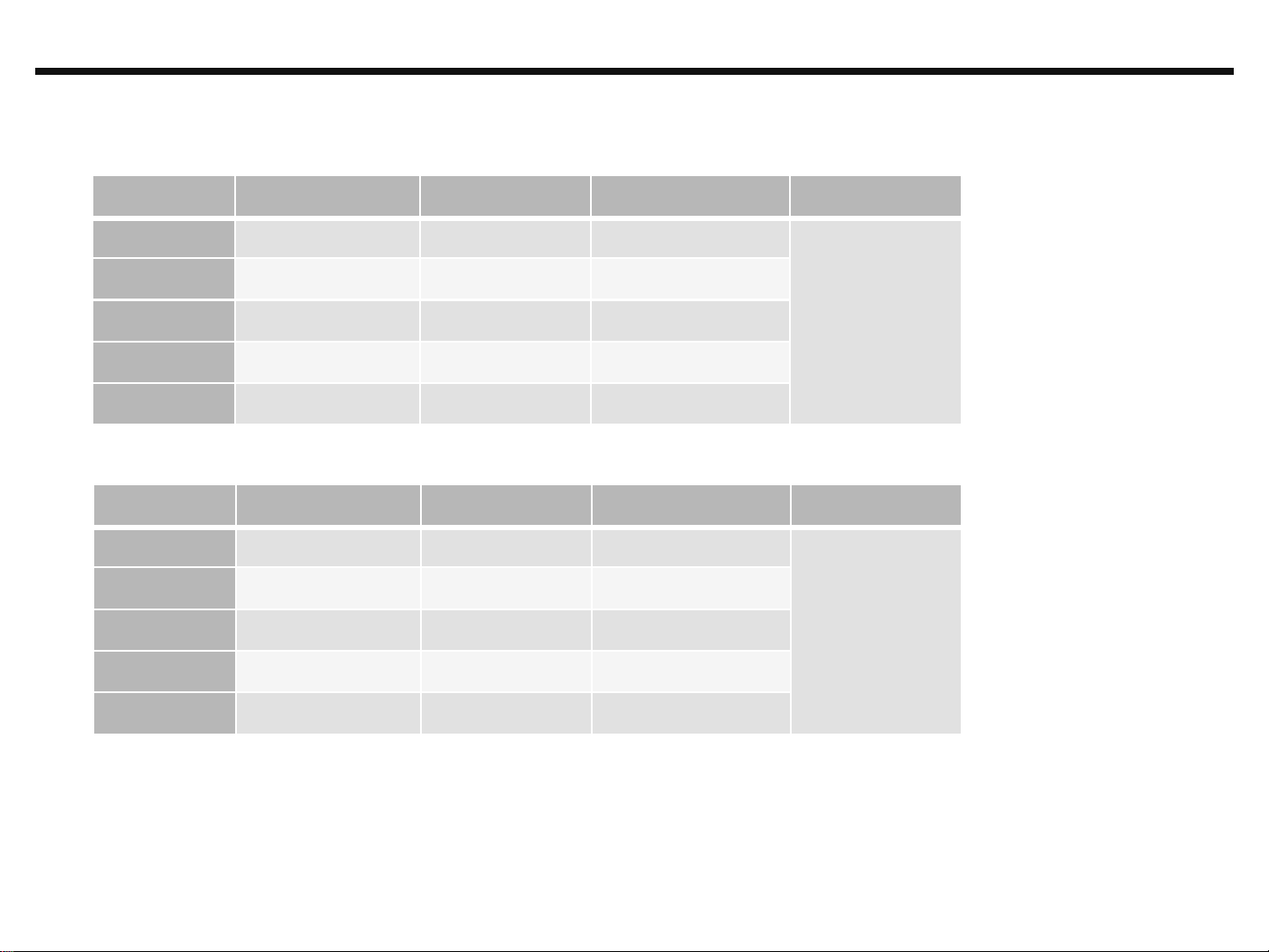
2. PERFORMANCE
2.1 Band Specification
Support Band
TX Freq (MHz)
RX Freq (MHz)
WCDMA(FDD1)
1920 – 1980
2110 – 2170
WCDMA(FDD2)
1852 – 1907
1932 – 1987
WCDMA(FDD5)
824 – 849
869 – 894
WCDMA(FDD8)
880 – 915
925 – 960
EGSM
880 – 915
925 – 960
GSM850
824 – 849
869 – 894
DCS1800
1710 – 1785
1805 – 1880
PCS1900
1850 – 1910
1930 – 1990
LTE3
1710 – 1785
1805 – 1880
LTE7
2500 – 2570
2620 – 2690
LTE28
703 – 748
758 – 803
5
Copyright ⓒ 2016 LG Electronics. Inc. All right
reserved. Only training and service purposes
http://vietmobile.vn
2. PERFORMANCE
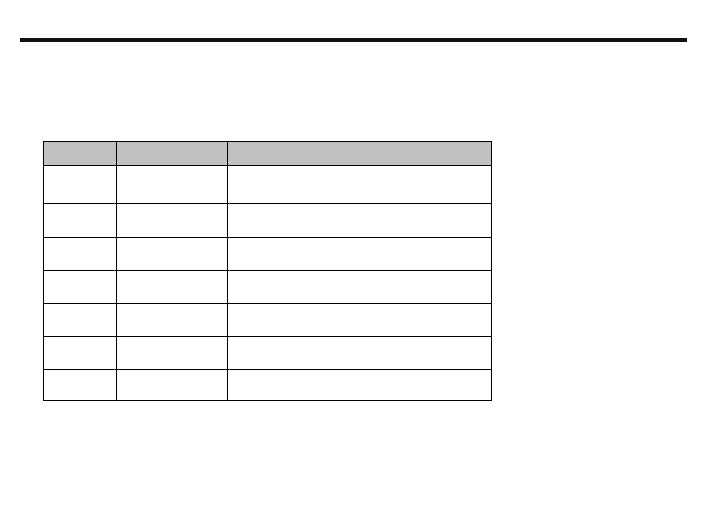
2.2 HW Features
List
Type / Spec.
1. Phone Type
DOP Type
2. Size
146.6 x 74.8 x 8.8
3. Weight
127.1 g ( with Battery )
4. Battery
2300mAh(Typ) (Li-Ion)
5.Chipset
MT6753 1.14GHz Octa core
6. Memory
16GB(EMMC) + 1.5GMB(LPDDR2)
7. LCD
Size
5.3 inch
Display Type
Active matrix TFT, Transmissive Type
Color
16.7M colors
Resolution
HD (720 x 1280)
8. Touch
Type
In-Cell Touch
9. Main Camera (13M)
Type
CMOS image sensor
Resolution
13MP @ 30 FPS
Focus (Laser / OIS)
AF (X/X)
# of Flash
1EA

6
Copyright ⓒ 2016 LG Electronics. Inc. All right
reserved. Only training and service purposes
http://vietmobile.vn
2. PERFORMANCE
2.2 HW Features
10. Audio
Receiver/Speaker/3.5phi
1 (AMR-WB) / 1 / Yes
# of mic.
2 Audio Zoom
X
11. Bluetooth
Standard
Bluetooth 4.0
Effective Distance
10M
Distance
0 m ~ 10 m (depend on environment)
12. WLAN
Standard
IEEE 802.11 b/g/n
Throughput
Max 40Mbps (SDIO Driver performance)
Depend on environment
0 ~ 50m (depend on environment)
13. GPS
type
A-GPS
14. FM
type
FM Radio, 3.5pi Ear-jack
7
Copyright ⓒ 2016 LG Electronics. Inc. All right
reserved. Only training and service purposes
http://vietmobile.vn
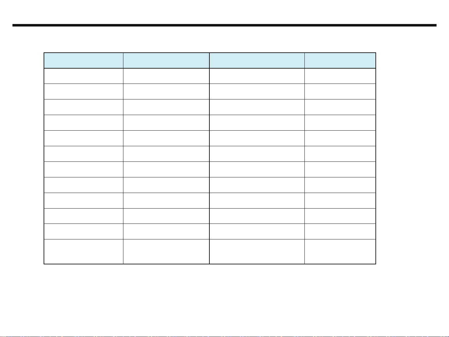
2. PERFORMANCE
2.3 RSSI Display
RSSI BAR
GSM RSSI
WCDMA RSCP
LTE RSRP
Comment
BAR 5->4
- 91dBm± 3dB
- 89dBm± 3dB
-85dBm ± 3dB
1. Call Connecte
d & CPIPH Level
=-3.3
2. LTE: RSRP
BAR 4->3
- 96dBm± 3dB
- 94dBm± 3dB
-95dBm ± 3dB
BAR 3->2
- 99dBm± 3dB
- 100dBm± 3dB
-105dBm ± 3dB
BAR 2->1
- 103dBm± 3dB
- 104dBm± 3dB
-115dBm ±3dB
BAR 1->0
- 105dBm± 3dB
- 110dBm± 3dB
-128dBm ± 3dB
RSSI BAR
GSM RSSI
WCDMA RSSI
LTE RSSI
Comment
BAR 5->4
- 91dBm± 3dB
- 86dBm± 3dB
-85dBm ± 3dB
1. Call Connecte
d & CPIPH Level
=-3.3
BAR 4->3
- 96dBm± 3dB
- 91dBm± 3dB
-95dBm ± 3dB
BAR 3->2
- 99dBm± 3dB
- 97dBm± 3dB
-105dBm ± 3dB
BAR 2->1
- 103dBm± 3dB
- 101dBm± 3dB
-115dBm ±3dB
BAR 1->0
- 105dBm± 3dB
- 107dBm± 3dB
-128dBm ± 3dB
8
Copyright ⓒ 2016 LG Electronics. Inc. All right
reserved. Only training and service purposes
http://vietmobile.vn
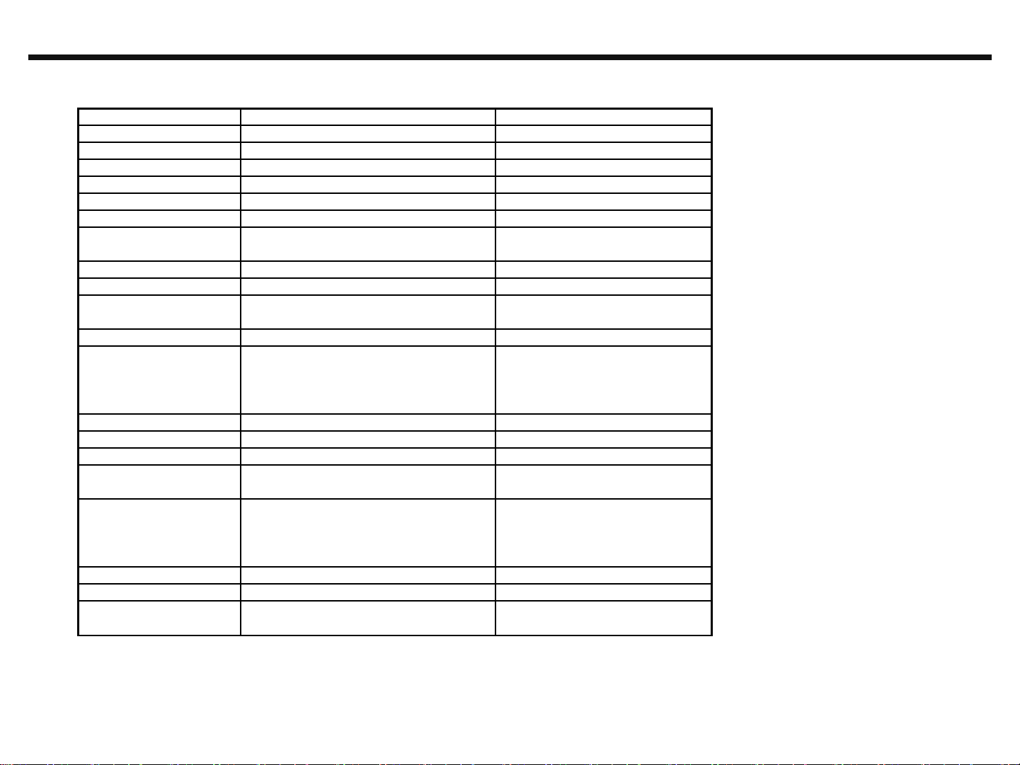
2. PERFORMANCE
2.4 Current consumption
구분
Specification
측정 조건
Sleep mode
(WCDMA)
320h over
7 mA under
DRX 7 @ BATT Capacity : 2300mAh
Sleep mode
(GSM)
320h over
7 mA under
EGSM P5 @ BATT Capacity : 2300mAh
Sleep mode
(LTE)
320h over
7 mA under
DRX 2.56 @ BATT Capacity :2300mAh (AMR Mode)
Calling
(WCDMA)
350m over
400mA under
10dBm @ BATT Capacity :2300mAh (AMR Mode)
Calling
(GSM)
350m over
400mA under
EGSM, LV5 @ BATT Capacity : 2300mAh
Calling
(LTE)
300m over
430mA under
Cat2 Tx 10dBm @ BATT Capacity : 2300mAh
Charging
time
4h 20m under
Phone off
-. Battery Spec. : 2,300mAh(Typ.)/3.8V/Li-Ion
9
Copyright ⓒ 2016 LG Electronics. Inc. All right
reserved. Only training and service purposes
http://vietmobile.vn
2. PERFORMANCE
2.5 Battery bar
Battery Bar
Specification
Battery Bar
Specification
Bar 20(Full)
98%
이상
Bar 9 -> Bar 8
43% -> 42%
Bar 20 -> Bar 19
98% -> 97%
Bar 8 -> Bar 7
38% -> 37%
Bar 19 -> Bar 18
93% -> 92%
Bar 7 -> Bar 6
33% -> 32%
Bar 18 -> Bar 17
88% -> 87%
Bar 6 -> Bar 5
28% -> 27%
Bar 17 -> Bar 16
83% -> 82%
Bar 5 -> Bar 4
23% -> 22%
Bar 16 -> Bar 15
78% -> 77%
Bar 4 -> Bar 3
16% -> 15%
Bar 15 -> Bar 14
73% -> 72%
Bar 3 -> Bar 2
13% -> 12%
Bar 14 -> Bar 13
68% -> 67%
Bar 2 -> Bar 1
8% -> 7%
Bar 13 -> Bar 12
63% -> 62%
Bar 1 -> Bar 0
3% -> 2%
Bar 12 -> Bar 11
58% -> 57%
Power off
1%
이하
Bar 11 -> Bar 10
53% -> 52%
Low battery pop-up
15% , 5%
Bar 10 -> Bar 9
48% -> 47%
high temperature pop-up
57도, 60도(Power off)
10
Copyright ⓒ 2016 LG Electronics. Inc. All right
reserved. Only training and service purposes
http://vietmobile.vn
2. PERFORMANCE
2.6 SW Specification
Item
Feature
Comment
RSSI
0 ~ 5 Levels
Battery Charging
0 ~ 20 Levels
Key Volume
0 ~ 7 Level
Audio Volume
0 ~ 15 Level
Time / Date Display
Yes
Multi-Language
Yes
depending on build language
Quick Access Mode
Phone / Messaging / Browser/ Appli
cations
Phone / Contact / Messaging /
Applications
PC Sync
Yes
Speed Dial
Yes
Voice mail center -> 1 key
Profile
Yes
not same with feature phone s
etting
CLIP / CLIR
Yes
Phone Book
Name / Number / Email / Groups /
Postal addresses / Organizations / I
M / Note / Nickname / Website / Ev
ent /
There is no limitation on the n
umber of items.
It depends on available memor
y amount.
Last Dial Number
Yes
Last Received Number
Yes
Last Missed Number
Yes
Search by Number/Na
me
Yes
Group
Yes
There is no limitation on the n
umber of items.
It depends on available memor
y amount.
Fixed Dial Number
Yes
Service Dial Number
No
Own Number
Yes
My Profile (add/edit/delete are
supported)

11
Copyright ⓒ 2016 LG Electronics. Inc. All right
reserved. Only training and service purposes
http://vietmobile.vn
2. PERFORMANCE
2.6 SW Specification
Voice Memo
Yes
Support voice recorder
Call Reminder
No
Network Selection
Automatic
Mute
Yes
Call Divert
Yes
Call Barring
Yes
Call Charge (AoC)
No
Call Duration
Yes
SMS (EMS)
There is no limitation on the number of items
.
It depends on available memory amount.
EMS does not support.
SMS Over GPRS
Yes
EMS Melody / Picture
Send / Receive / Save
No
MMS MPEG4
Send / Receive / Save
Yes
Send / Receive : Yes
Save : depends on contenttype
Support video content type li
st
1.
video/mp4
2.
video/h263
3.
video/3gpp2
video/3gpp
Long Message
MAX 2000 characters
The standard of Open vender
Cell Broadcast
Yes
Download
Over the Web
Game
No
Calendar
Yes
Memo
Yes
There is no limitation on the number o
f items.
It depends on available memory amo
unt.
World Clock
Yes

12
Copyright ⓒ 2016 LG Electronics. Inc. All right
reserved. Only training and service purposes
http://vietmobile.vn
2. PERFORMANCE
2.6 SW Specification
Unit Convert
No
Stop Watch
Yes
Wall Paper
Yes
WAP Browser
No
Support only web browser bas
ed on webkit. WAP stack and
wml are not supported.
Download Melody /
Wallpaper
Yes
Over web browser
SIM Lock
No
SIM Toolkit
Yes
MMS
Yes
OMA MMS 1.2 version
EONS
Yes
CPHS
Yes
V4.2
ENS
No
Camera
Yes
13MP AF / 5MP
Digital Zoom : x4
JAVA
No
Voice Dial
No
US English only
IrDa
No
IrRC
Bluetooth
Yes
Ver. 4.2LE [HSP, HFP, A2DP, AVR
CP, PBAP, OPP, MAP, HID, PAN,
HOGP, HDP, DID]
FM radio
Yes
GPRS
Yes
Class 12
EDGE
Yes
Class 12(Rx only)
Hold / Retrieve
Yes
Conference Call
Yes
Max. 6
DTMF
Yes
Memo pad
No
TTY
No
AMR
Yes
SyncML
No
IM
Yes
Google Hangout
Email
Yes
IMAP/POP3/SMTP/EAS
13
Copyright ⓒ 2016 LG Electronics. Inc. All right
reserved. Only training and service purposes
http://vietmobile.vn
3. TROUBLE SHOOTING
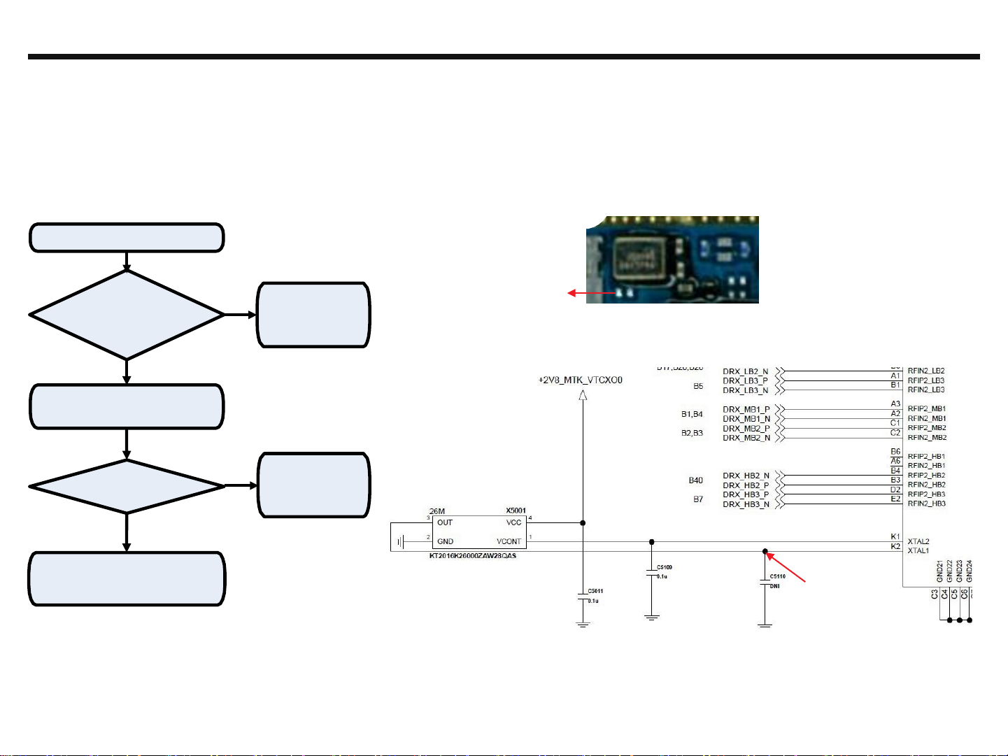
3.1 Checking XO Block
TP1
Main
Top
TP1
START
Check TP1
Is it 26MHz?
NO
Replace X5001 and then
check TP1
Is it 26MHz?
NO
The Problem may be
Logic part
Refer to Logic trouble shoot
The out put frequency(26MHz) of VTCXO(X5001) is used as the reference one of MT6169
Checking Flow
X5001
XO Circuit is OK.
YES
YES
Check next step
Circuit Diagram
XO Circuit is OK.
Check next step
Image
14
Copyright ⓒ 2016 LG Electronics. Inc. All right
reserved. Only training and service purposes
http://vietmobile.vn
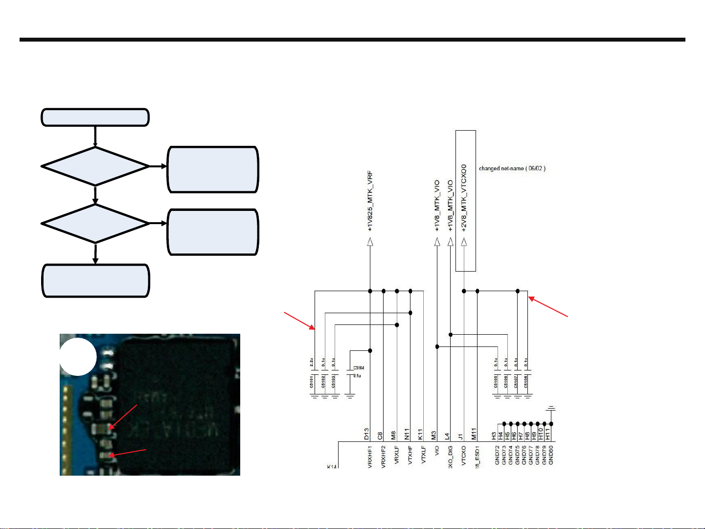
3. TROUBLE SHOOTING
3.2 Checking Transceiver DC Power Supply Circuit Block
Main
Bot
TP1
TP2
START
Check TP1
+2.8V_RF is OK?
The Problem may be
Logic part
NO
Refer to
Logic trouble shoot
YES
Check TP2
The Problem may be
+1.8V_RF is OK?
NO
Logic part
Refer to
Logic trouble shoot
YES
Check next step
The MT6169 operating voltages used two voltage sources 1.8V and 2.8V
Checking Flow
Circuit Diagram
Image
TP1
TP2
15
Copyright ⓒ 2016 LG Electronics. Inc. All right
reserved. Only training and service purposes
http://vietmobile.vn
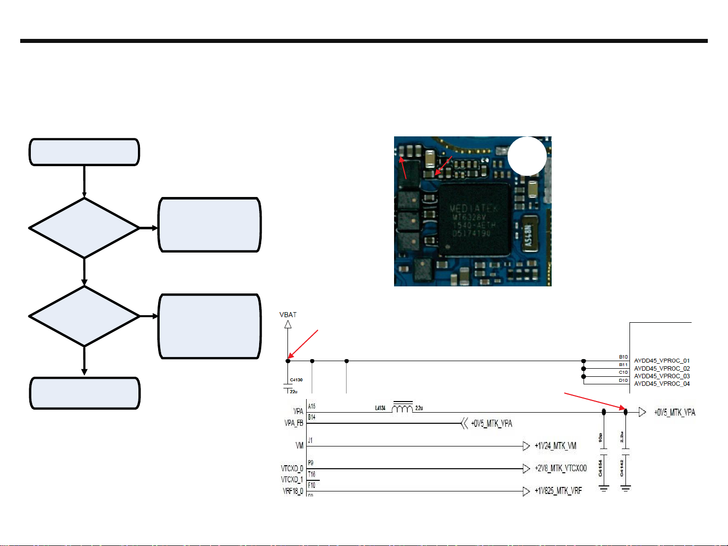
3. TROUBLE SHOOTING
3.3 Checking DC-DC Block
Main
Bot
TP2
TP1
Circuit Diagram
START
Check TP1
VBAT is OK?
The Problem may be
Logic part
Refer to Logic trouble
shoot
YES
Check TP2
0.5V ≤ TP2 ≤ 4.2V ?
Check U4100 Physical
NO
Damage or soldering
condition
YES
Check next step
The DC-DC(MT6328, U4100) output voltages is used as the reference one of SKY77643-31
Checking Flow
NO
Image
TP1
U4100
TP2
16
Copyright ⓒ 2016 LG Electronics. Inc. All right
reserved. Only training and service purposes
http://vietmobile.vn
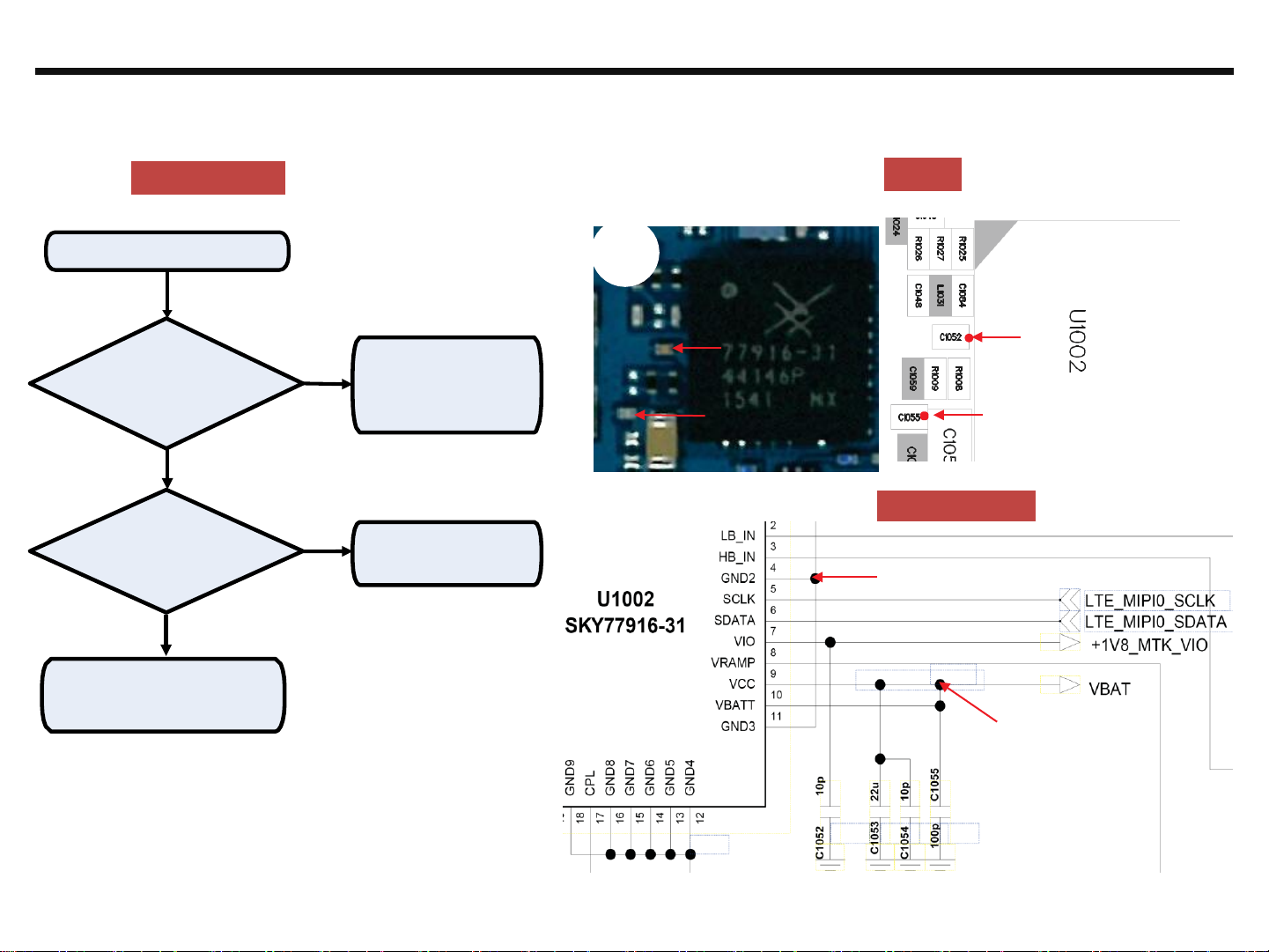
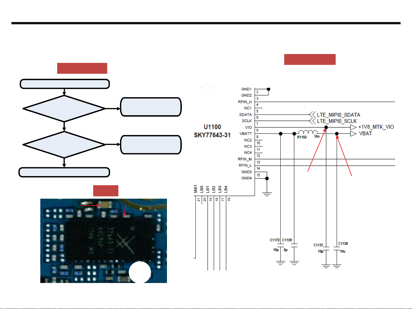
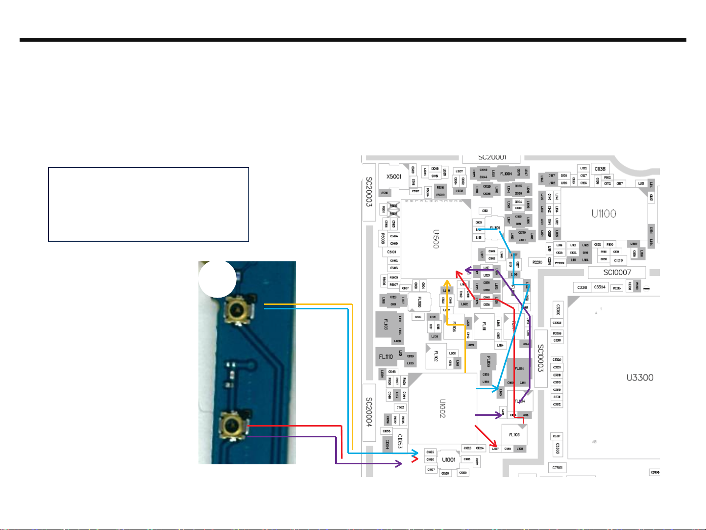
3. TROUBLE SHOOTING
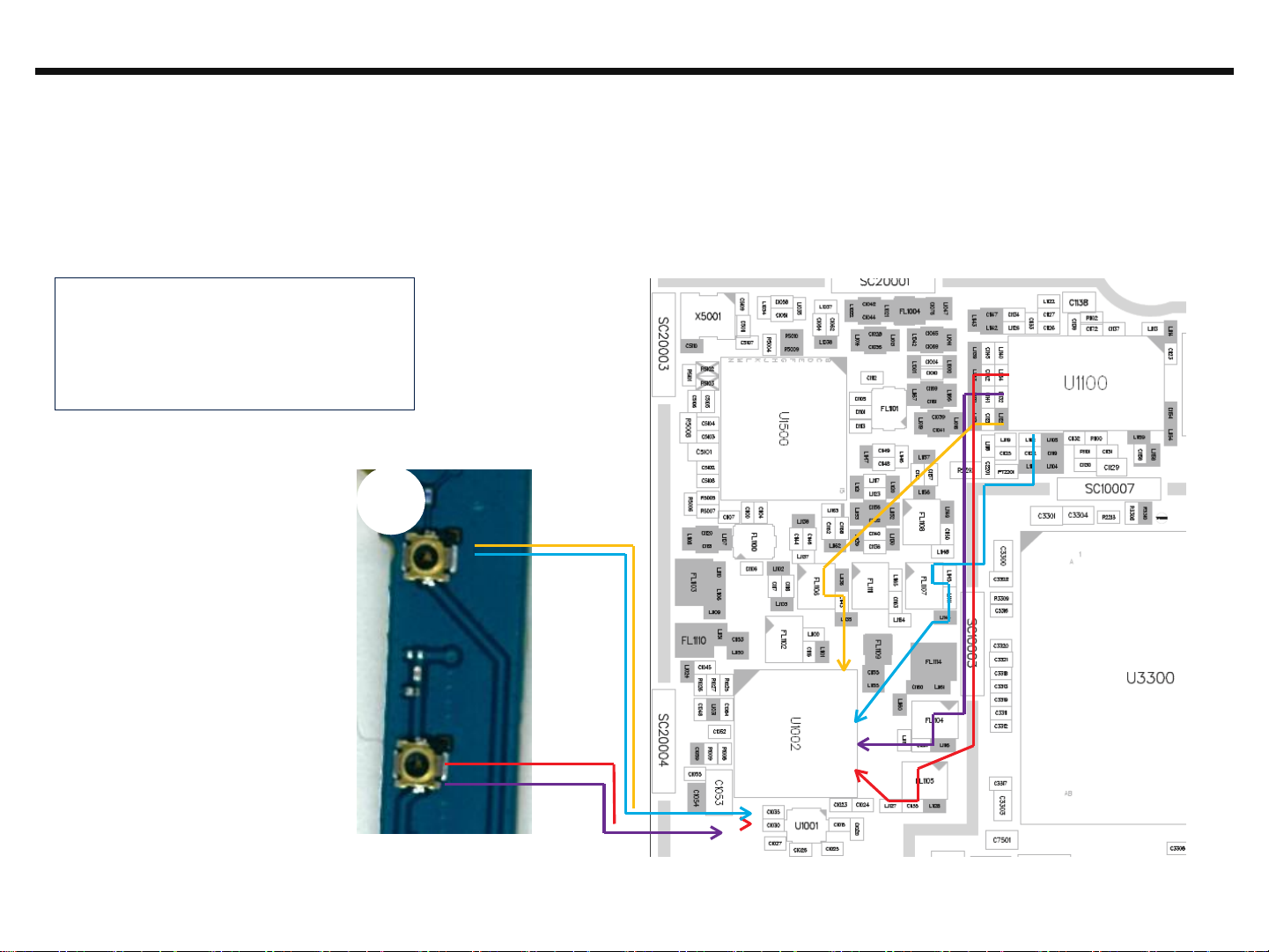
3.4 ASM(Antenna Switch Module) Block
Main
Top
TP2
START
Check TP1, TP2 High Level ?
(2.5V≤TP1 ≤3.1V)
(3.9V≤TP2 ≤4.2V)
The Problem may be
Logic part
Refer to Logic trouble
shoot
YES
Check U1002 physical Damage
or soldering condition
Replace U1002
OK?
Check Next step
3.4.1 Checking ANT #1 ASM (GSM 850/900, W B5/8, LTE B7/20)
Checking Flow
NOT GOOD
NO
TP1
Image
U1002
TP1
TP2
Circuit Diagram
TP1
TP2
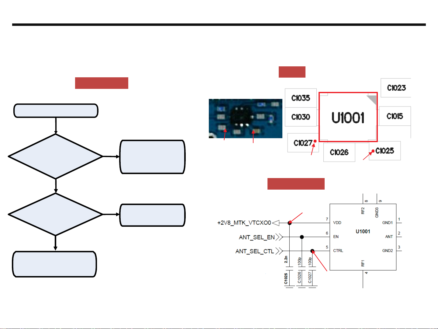
17
Copyright ⓒ 2016 LG Electronics. Inc. All right
reserved. Only training and service purposes
http://vietmobile.vn
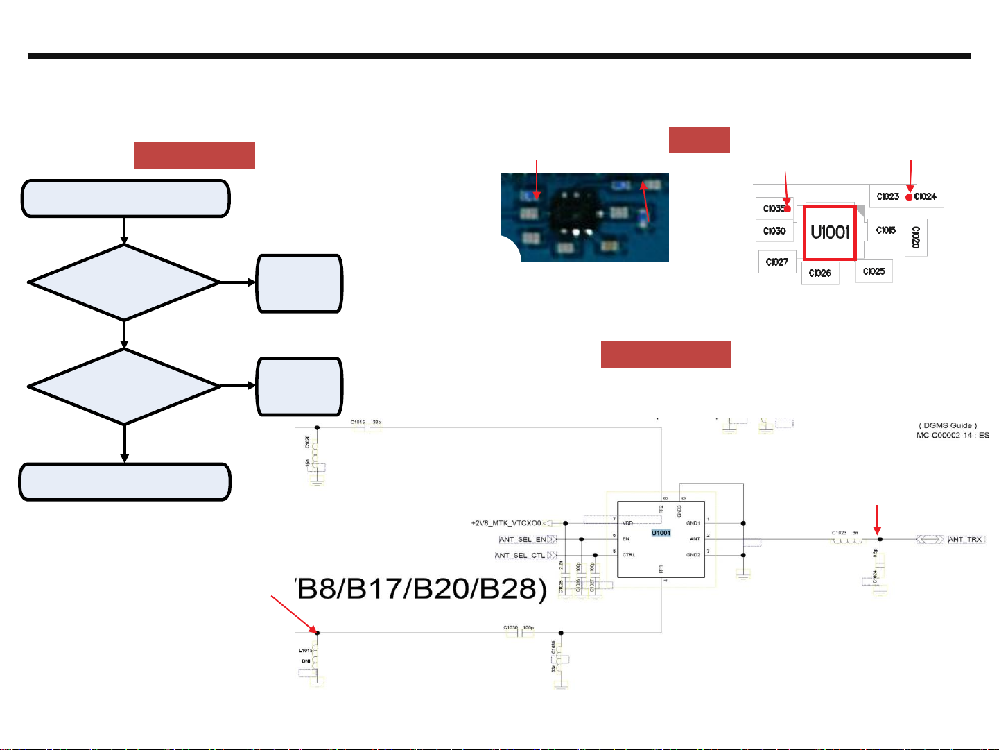
3. TROUBLE SHOOTING
3.4 ASM(Antenna Switch Module) Block
TP2
U1001
TP2
TP1
TP2
START
Check TP1, TP2 High Level ?
(2.5V≤TP1 ≤3.1V)
(1.7V≤TP2 ≤1.9V)
The Problem may be
Logic part
Refer to Logic trouble
shoot
YES
NOT GOOD
Check U1001 physical Damage
or soldering condition
Replace U1001
Check Next step
3.4.2 Checking ANT #2 ASM (GSM 1800/1900, W B1 B2, LTE B3)
Checking Flow
Image
NO
OK?
TP1
Circuit Diagram
TP1
18
Copyright ⓒ 2016 LG Electronics. Inc. All right
reserved. Only training and service purposes
http://vietmobile.vn
3. TROUBLE SHOOTING
3.5 GSM RF PART
GSM RF Part support GSM850/900/1800/1900 with ASM, PAM, Transceiver component
Checking Flow
START
Check XO Block
Refer 3.1
Check Transceiver DC Power supply Block
Refer 3.2
Check DC-DC Block
Refer 3.3
Check ASM Block
Refer 3.4
Check T/RX Block
Re-Download & Cal
Change the Board
19
Copyright ⓒ 2016 LG Electronics. Inc. All right
reserved. Only training and service purposes
http://vietmobile.vn
3. TROUBLE SHOOTING
3.5 GSM RF PART
Main
Top
Main
BOT
1.
GSM850 RX PATH
2.
GSM900 RX PATH
3.
GSM1800 RX PATH
4.
GSM1900 RX PATH
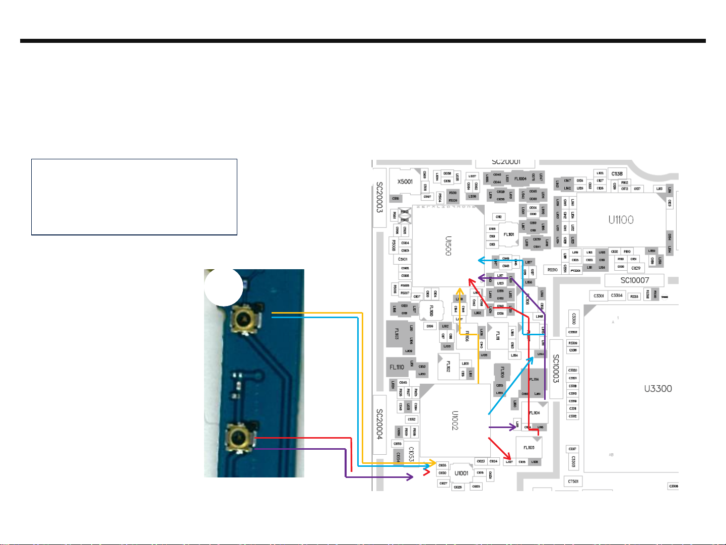
3.5.1 GSM RF Part RX RF PATH
Image
SW1001
SW1002
20
Copyright ⓒ 2016 LG Electronics. Inc. All right
reserved. Only training and service purposes
http://vietmobile.vn
3. TROUBLE SHOOTING
START
Check TP1 Signal exist?
Check
SW1002
NO
Soldering
YES
Check TP2 Signal exist?
NO
YES
Check next step
3.5 GSM RF PART
U1001
3.5.2 Checking RF Signal RX path(SW, GSM850/900)
Checking Flow
Check
U1001
Soldering
Main
Top
TP1 TP2
Circuit Diagram
Image
TP1
TP2
TP2
TP1
21
Copyright ⓒ 2016 LG Electronics. Inc. All right
reserved. Only training and service purposes
http://vietmobile.vn
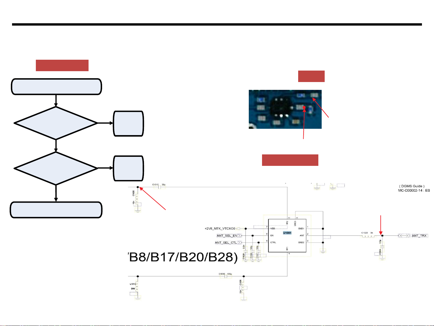
3. TROUBLE SHOOTING
3.5 GSM RF PART
TP2
TP1
TP3
Main
Top
START
Check TP1/2 Signal exist?
NO
Replace U1002
YES
Check TP3/4 Signal exist?
NO
Check
Component
above RF signal
path
YES
Check Transceiver
physical damage
or soldering condition
Replace U1500
NOT GOOD
OK?
Check next step
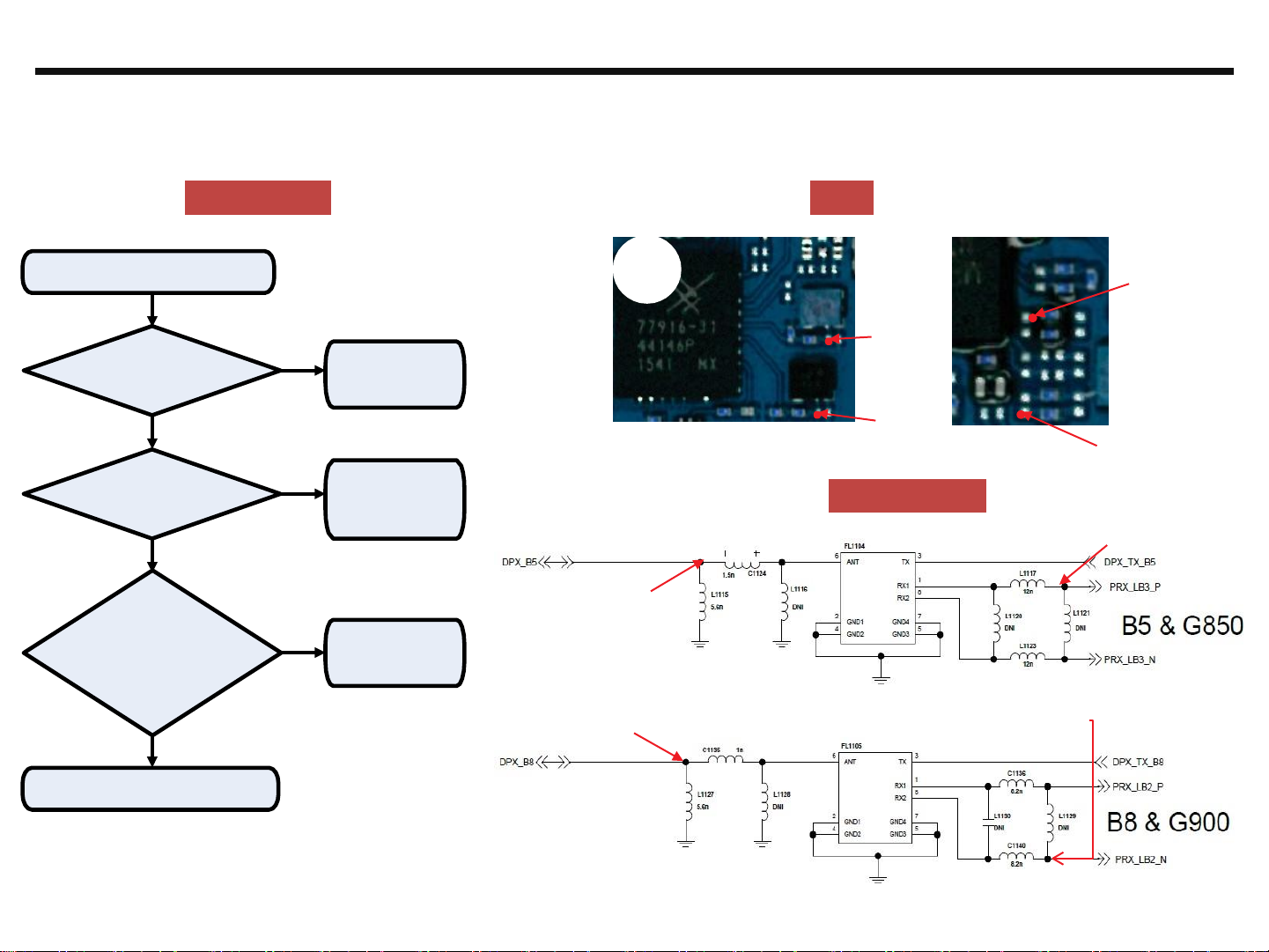
3.5.3 Checking RF Signal RX path(GSM850/900)
Checking Flow Image
FL1104
TP4
TP2
FL1105
Circuit Diagram
TP1
TP3
TP4
22
Copyright ⓒ 2016 LG Electronics. Inc. All right
reserved. Only training and service purposes
http://vietmobile.vn
3. TROUBLE SHOOTING
3.5 GSM RF PART
3.5.4 Checking RF Signal RX path(SW, GSM1800/1900)
Checking Flow
START
Image
Main
Top
Check TP1 Signal exist?
YES
Check TP2 Signal exist?
YES
Check next step
NO
NO
Check
SW1100
Soldering
Check
U1001
Soldering
TP1
U1001
TP1
Circuit Diagram
TP2
TP2
23
Copyright ⓒ 2016 LG Electronics. Inc. All right
reserved. Only training and service purposes
http://vietmobile.vn
3. TROUBLE SHOOTING
3.5 GSM RF PART
TP1
TP4
TP2
TP1
START
Check TP1/2 Signal exist?
Replace U1002
Check TP3/4 Signal exist?
Check Component
above RF signal
path
Check Transceiver
physical damage
or soldering condition
Replace U1500
NOT
GOOD
OK?
Check next step
3.5.5 Checking RF Signal RX path(GSM1800/1900)
Image
Checking Flow
YES
YES
NO
NO
TP4
TP3
Circuit Diagram
TP2
TP3
24
Copyright ⓒ 2016 LG Electronics. Inc. All right
reserved. Only training and service purposes
http://vietmobile.vn
3. TROUBLE SHOOTING
3.5 GSM RF PART
Main
BOT
1.
GSM850 TX PATH
2.
GSM900 TX PATH
3.
GSM1800 TX PATH
4.
GSM1900 TX PATH
3.5.6 GSM RF Part TX RF PATH
SW1001
SW1002
25
Copyright ⓒ 2016 LG Electronics. Inc. All right
reserved. Only training and service purposes
http://vietmobile.vn
3. TROUBLE SHOOTING
3.5 GSM RF PART
The Problem may be
Other part
Check Logic part
YES
Check TP2
1.5V≤TP2≤ 2V?
YES
Check Next step
TP1
TP2
3.5.7 Checking GSM PAM DC Power Circuit
Checking Flow
START
Check TP1
+VPWR OK?
NO
NO
Check DC-DC Power
Refer to 1.8V
Circuit Diagram
Block
Image
TP2
TP1
Main
Top
26
Copyright ⓒ 2016 LG Electronics. Inc. All right
reserved. Only training and service purposes
http://vietmobile.vn
3. TROUBLE SHOOTING
3.5 GSM RF PART
U1001
TP2
Main
Top
START
Check TP1 Signal exist?
Check
U1001
NO
Soldering
YES
Check TP2 Signal exist?
Check
U1002
NO
Soldering
YES
Check next step
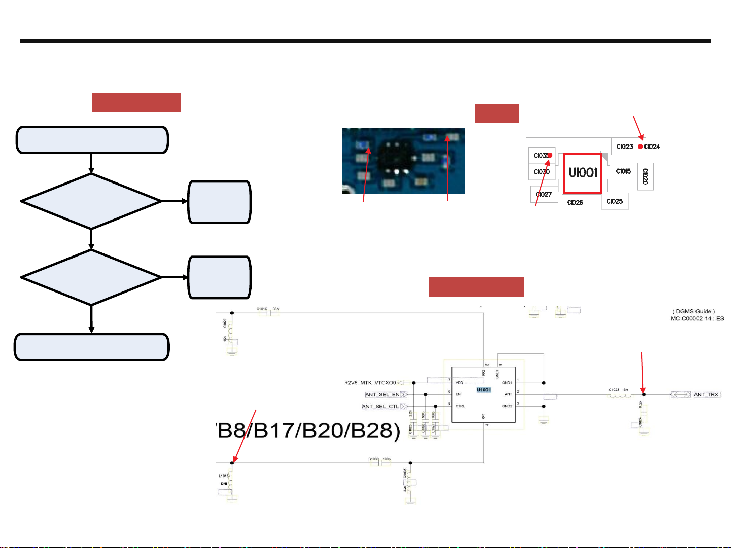
3.5.8 Checking RF Signal TX path(SW, GSM850/900)
Checking Flow
TP1
Image
Circuit Diagram
TP1
TP2
TP2
TP1
27
Copyright ⓒ 2016 LG Electronics. Inc. All right
reserved. Only training and service purposes
http://vietmobile.vn
3. TROUBLE SHOOTING
3.5 GSM RF PART
Main
Top
START
NO
Check TP1/2
If GSM850/900 Over 9dBm?
NO
Check Transceiver
physical damage
or soldering condition
OK?
Check next step
3.5.9 Checking RF Signal TX path(GSM850/900)
Checking Flow
TP2
Image
U1100
TP2
YES
NOT GOOD
TP1
TP1
Replace U1100
Circuit Diagram
Replace U1500
TP2
TP1
28
Copyright ⓒ 2016 LG Electronics. Inc. All right
reserved. Only training and service purposes
http://vietmobile.vn
3. TROUBLE SHOOTING
3.5 GSM RF PART
3.5.10 Checking RF Signal TX path(GSM1800/1900)
Checking Flow Image
START
Main
Top
NO
Check TP1/2
If GSM1800/1900 Over
9dBm?
NO
Check Transceiver
physical damage
or soldering condition
OK?
Check next step
YES
NOT GOOD
Replace U1100
Replace U1500
TP2
TP1
TP2
U1100
TP1
Circuit Diagram
TP1
TP2

29
Copyright ⓒ 2016 LG Electronics. Inc. All right
reserved. Only training and service purposes
http://vietmobile.vn
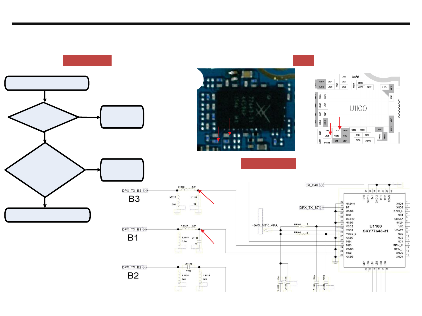
3. TROUBLE SHOOTING
3.6 WCDMA RF PART
WCDMA RF Part support WCDMA B1/2/5/8 with ASM, PAM, Transceiver component
Checking Flow
START
Check XO Block
Refer 3.1
Check Transceiver DC Power supply Block
Refer 3.2
Check DC-DC Block
Refer 3.3
Check ASM Block
Refer 3.4
Check T/RX Block
Re-Download & Cal
Change the Board
30
Copyright ⓒ 2016 LG Electronics. Inc. All right
reserved. Only training and service purposes
http://vietmobile.vn
3. TROUBLE SHOOTING
3.6 WCDMA RF PART
Main
Top
Main
BOT
1.
WCDMA B5 RX PATH
2.
WCDMA B8 RX PATH
3.
WCDMA B1 RX PATH
4.
WCDMA B2 RX PATH
3.6.1 WCDMA RF Part RX RF PATH
Image
SW1001
SW1002
 Loading...