

LG GM76C8128CLL-70, GM76C8128CLL-55, GM76C8128CLLE-55, GM76C8128CLL-85, GM76C8128CLLI-85 Datasheet
...
GM76C8128CL/CLL
131,072 WORDS x 8 BIT
CMOS STATIC RAM
Description
Features
* Fast Speed : 55/70/85ns
* Low Power Standby and Low Power Operation
Standby : 0.275mW Max. at TA = - 40 ~ 85C(LLE/LLI)
0.55mW Max. at TA = - 40 ~ 85C(LE/LI)
0.11mW Max. at TA = 0 ~ 70C(LL)
0.55mW Max. at TA = 0 ~ 70C(L)
Operation : 385mW (Max)
* Completely Static RAM : No Clock or Timing
Strobe Required
* Equal Access and Cycle Time
* TTL compatible inputs and outputs
* Capability of Battery Back-up Operation
* Single + 5V+/-10% Operation
* Standard 32 DIP, SOP and TSOP-I,STSOP-I
* Temperature Range
Commercial(0¡-70C) : GM76C8128C
Extended (-25 ~ 85C) : GM76C8128C-E
Industrial (-40 ~ 85C) : GM76C8128C-I
The GM76C8128CL/CLL is a 1,048,576 bits static
random access memory organized as 131,072 words
by 8 bits. Using a 0.6um advanced CMOS technology
and it provides high speed operation with minimum
cycle time of 55/70/85ns. The device is placed in a
low power standby mode with /CS1 high or CS2 low
and the output enable (/OE) allows fast memory
access. Thus it is suitable for high speed and low
power applications, especially where battery back-up
is required.
85
Pin Description
I/O0
I/O1
I/O2
I/O3
I/O4
I/O5
I/O6
I/O7
Pin Function
A0-A16 Address Inputs
I/O0-I/O7
VCC
VSS
Write Enable Input
Chip Select Input
Output Enable Input
Data Inputs/Outputs
Power Supply (4.5V ~5.5V)
Ground
NC No Connection
/WE
/CS1, CS2
/OE
Pin Configuration
(Top View)
A7
A6
A5
A4
A3
A2
A1
A0
VCC
A15
CS2
/WE
A13
A8
A9
A11
/OE
A10
/CS1
I/O7
1
2
3
4
5
6
7
8
9
10
11
12 21
22
23
24
25
26
27
28
29
30
31
32
I/O0
I/O1
I/O6
I/O5
13
14 19
20
I/O2
VSS
I/O4
I/O3
15
16 17
18
NC
A16
A14
A12
Block Diagram
MEMORY CELL ARRAY
1024 x 128 x 8
(128K x 8)
Column Select
I/O Buffer
Address
Buffer
X
Decoder
10
1024
7
128
128 x 8
8
Y
Decorder
/CS1, CS2
A0
A1
A2
A14
A15
A16
/CS1
/OE
. . . . . . . .
Chip
Control
/OE, /WE
Chip
Control
/WE
CS2
LG Semicon Co.,Ltd.

GM76C8128CL/CLL
86
Absolute Maximum Ratings*
*: Stresses greater than those listed under "Absolute Maximum Ratings" may cause permanent damage to the device.
This is a stress rating only and functional operation of the device at these or any other conditions above those indi cated in the operating sections of this specification is not implied. Exposure to absolute maximum rating conditions
for extended periods may affect reliability.
Recommended DC Operating Conditions (TA = - 40 ~ 85C)
Truth Table
*Note: X means don't care
/CS1
L
L
L
CS2
H
H
H
/OE
L
X
H
A0 to A16
Stable
Stable
Stable
DATA I/O
Output Data
Input Data
Hi-Z
MODE
Read
Write
Output Disable
H X X - Hi-Z
Standby
X L X - Hi-Z
/WE
H
L
H
X
X
Symbol Parameter Unit
VCC
VIH
VIL
Supply Voltage
Input High Voltage
Input Low Voltage
V
V
V
Max
5.5
VCC + 0.3
0.8
Typ
5.0
-
-
Min
4.5
2.2
-0.3*
*Note :VIL(min) = -3.0V for <= 10ns pulse
Symbol Parameter Rating Unit
TA
TSTG
TSOL
-25 ~ 85
-55 ~ 150
260, 10 (at lead)
Ambient Temperature under Bias
Storage Temperature
Soldering Temperature and Time
C
C
C, S
VCC -0.3 ~ 7.0Supply Voltage V
VIN
VI/O -0.5 ~ VCC + 0.5
Input Voltage
Input and Output Voltage
V
V
PD 1.0Power Dissipation W
C
C-40 ~ 85
0 ~ 70
GM76C8128C-E
GM76C8128C-I
GM76C8128C
Capacitance (f = 1MHZ, TA = 25C)
Symbol Parameter Unit
CIN
CI/O
Input Capacitance
Output Capacitance
pF
pF
Max
6
8
MinTest Conditions
VI = 0V
VO = 0V
-
-
*Note: This parameter is sampled and not 100% tested.
-0.3 ~ 7.0
GM76C8128CL/CLL
87
DC Operating Characteristics (VCC = 5V+/-10%, TA = - 40 ~ 85C)
*Typ. Values are measured at 25C
Symbol Parameter
II(L) Input Leakage Current
IO(L) Output Leakage Current
VOH High Level Output Voltage
VOL Low Level Output Voltage
ICC
Operating Supply Current
ICC1
Average Operating Current
ICC2
ICCS1
ICCS2
Standby Current(TTL)
Conditions
VIN = 0 to VCC
/CS1 = VIH or CS2 = VIL
/OE = VIH, VSS <=VOUT<=VCC
IOH = -1.0mA
IOL = 2.1mA
/CS1 = VIL and CS2 = VIH
VIN = VIH/VIL, IOUT = 0mA
/CS1 = VIL and CS2 = VIH
VIN = VIH/VIL
IOUT = 0mA
tcycle = Min, cycle
/CS1 = 0.2V, CS2 = VCC-0.2V
VIN = VCC - 0.2V/0.2V
IOUT = 0mA
tcycle = 1us
/CS1 = VIH, CS2 = VIL
/CS1 = VCC-0.2V
CS2 = 0.2V
Unit
uA
uA
V
V
mA
mA
mA
mA
Max
1
1
-
0.4
15
70
10
2
*Typ
-
-
-
-
-
Min
-1
-1
2.4
-
-
-
-
-
uA
uA
100
50
-
-
-
-
-
-
-
-
-
GM76C8128C-E
GM76C8128C-I
GM76C8128C
Standby
Current(CMOS)
100
20
-
-
L - Version
LL - Version
L - Version
LL - Version
Test Conditions (VCC = 5V+/-10%, TA = - 40 ~ 85C, unless otherwise noted.)
AC Operating Characteristics
Parameter
Input Pulse Level
Input Rise and Fall Time
Value
0.6V to 2.4V
5ns
Input and Output Timing Reference Levels 1.5V
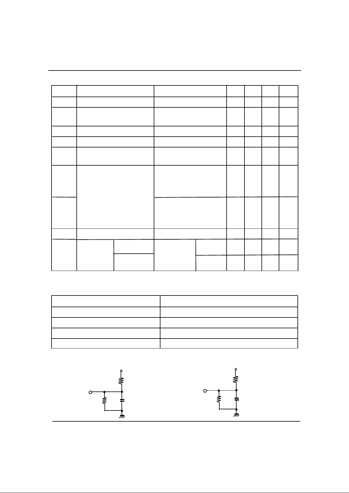
Output Load See below
Output Load (A)
Output Load (B) (for tCHZ, tCLZ, tWHZ, tOW, tOLZ & tOHZ)
+5V
DOUT
1.8K§Ù
990§Ù
5 §Ü*
+5V
DOUT
1.8K§Ù
990§Ù
100 §Ü*

GM76C8128CL/CLL
88
AC Operating Characteristics (VCC = 5V+/-10%, TA = - 40 ~ 85C)
Symbol Parameter Unit
tRC Read Cycle Time
tAA Address Access Time
tACS1 Chip Select 1 Access Time
tACS2 Chip Select 2 Access Time
tOE Output Enable Access Time
tCLZ1 Chip Select 1 Output Setup Time
tCHZ1 Chip Select 1 Output Floating
tCLZ2 Chip Select 2 Output Setup Time
tCHZ2 Chip Select 2 Output Floating
tOLZ Output Enable Output Setup Time
tOHZ Output Enable Output Floating
tOH Output Hold Time
MaxMin
ns
ns
ns
ns
ns
ns
ns
ns
ns
ns
ns
ns
85
85
85
45
30
30
30
-
85
-
-
-
-
10
-
10
-
0
-
10
55
55
55
30
20
20
20
-
55
-
-
-
-
5
-
5
-
0
-
5
Write Cycle
Symbol Parameter Unit
tWC Write Cycle Time
tCW1 Chip Select Time 1
tCW2 Chip Select Time 2
tAW Address Enable Time
tAS Address Setup Time
tWP Write Pulse Width
tWR Address Hold Time
tDW Input Data Setup Time
tDH Input Data Hold Time
tWHZ Write to Output in High-Z
tOW Output Active from End of Write
MaxMin
ns
ns
ns
ns
ns
ns
ns
ns
ns
ns
ns
-85-55
-
50
50
50
0
0
0
0
45
25
20
-
-
-
-
-
-
-
-
-
-
75
75
70
0
0
0
0
60
35
30
-
-
-
-
-
-
-
-
-
Read Cycle
MaxMin MaxMin
MaxMin MaxMin
70
70
70
35
25
25
25
-
70
-
-
-
-
5
-
5
-
0
-
10
-70
-
65
65
60
0
0
0
0
50
30
25
-
-
-
-
-
-
-
-
-
GM76C8128C-55 GM76C8128C-70 GM76C8128C-85
GM76C8128C-55 GM76C8128C-70 GM76C8128C-85
 Loading...