

LG GM730 Service Manual

Service Manual Model : GM730
Internal Use Only
Service Manual
GM730
Date: May 2009 / Issue 1.0

Table Of Contents
1. INTRODUCTION ...............................................5
1.1 Purpose ......................................................................5
1.2 Regulatory Information .................................................5
2. PERFORMANCE ...............................................7
2.1 System Overview .........................................................7
2.2 Usable environment .....................................................8
2.3 Radio Performance ......................................................9
2.4 Current Consumption ................................................13
2.5 RSSI BAR ..................................................................14
2.6 Battery BAR ..............................................................14
3. TECHNICAL BRIEF .........................................15
3.1 GENERAL DESCRIPTION .............................................15
3.2 GSM MODE ...............................................................16
3.3 UMTS MODE .............................................................20
3.4 GPS MODE ...............................................................23
3.5 LO GENERATION and DISTRIBUTION CIRCUIT ..............23
3.6 OFF-CHIP RF COMPONENTS ......................................24
3.7 Main Features ...........................................................28
3.8 Digital Baseband(DBB/MSM7200A) ............................33
3.9 Hardware Architecture ...............................................34
3.10 Subsystem(MSM7200A) ..........................................36
3.11 Power Block ............................................................39
3.12 External memory interface .......................................44
3.13 H/W Sub System .....................................................46
3.14 Audio and sound .....................................................55
3.15 Camera interface .....................................................62
3.16 Proximity Sensor .....................................................69
3.17 Luminance Sensor ...................................................70
3.18 Motion Sensor .........................................................71
4. TROUBLE SHOOTING ..................................... 72
4.1 RF Component ..........................................................72
4.2 SIGNAL PATH ............................................................74
4.3 Checking TCXO Block ................................................78
4.4 Checking Front End Module(FEM) Block ......................80
4.5 Checking WCDMA Block ............................................83
4.6 Checking GSM Block .................................................95
4.7 Power ON Troubleshooting .......................................102
4.8 Charger Troubleshooting ..........................................104
4.9 USB trouble .............................................................107
4.10 Audio trouble .........................................................109
4. 11 5M Camera trouble ...............................................119
4.12 VGA Camera trouble ..............................................122
4.13 Main LCD trouble ..................................................125
4.14 SIM Detect Troubleshooting ....................................127
4.15 Keypad Backlight Troubleshooting ...........................129
4.16 LINEAR MOTOR .....................................................130
4.17 Proximity Sensor on/off trouble ...............................131
4.18 Luminance Sensor on/off trouble ............................133
4.19 Motion Sensor on/off trouble ..................................135
5. Downloading .............................................. 137
5.1 Introduction .............................................................137
5.2 Downloading Procedure ...........................................138
6. BLOCK DIAGRAM ........................................ 147
7. CIRCUIT DIAGRAM ...................................... 157
8. BGA Pin Map .............................................. 165
9. PCB LAYOUT ...............................................173
10. Calibration & RF Auto Test Program
(Tachyon) .................................................. 177
10.1 Confi guration of Tachyon .......................................177
10.2 How to use Tachyon ...............................................179
11. Test Mode ................................................. 182
12. EXPLODED VIEW & REPLACEMENT
PART LIST ................................................ 191
12.1 EXPLODED VIEW ...................................................191
12.2 Replacement Parts ................................................193
12.3 Accessory ............................................................. 219
Copyright © 2009 LG Electronics. Inc. All right reserved.
Only for training and service purposes
- 3 -
LGE Internal Use Only

LGE Internal Use Only Copyright © 2009 LG Electronics. Inc. All right reserved.
- 4 -
Only for training and service purposes

1. INTRODUCTION
1.1 Purpose
This manual provides the information necessary to repair, calibration, description and download the
features of this model.
1.2 Regulatory Information
A. Security
Toll fraud, the unauthorized use of telecommunications system by an unauthorized part (for example,
persons other than your company’s employees, agents, subcontractors, or person working on your
company’s behalf) can result in substantial additional charges for your telecommunications services.
System users are responsible for the security of own system. There are may be risks of toll fraud
associated with your telecommunications system. System users are responsible for programming and
configuring the equipment to prevent unauthorized use. The manufacturer does not warrant that this
product is immune from the above case but will prevent unauthorized use of common-carrier
telecommunication service of facilities accessed through or connected to it. The manufacturer will not
be responsible for any charges that result from such unauthorized use.
B. Incidence of Harm
If a telephone company determines that the equipment provided to customer is faulty and possibly
causing harm or interruption in service to the telephone network, it should disconnect telephone
service until repair can be done. A telephone company may temporarily disconnect service as long as
repair is not done.
C. Changes in Service
A local telephone company may make changes in its communications facilities or procedure. If these
changes could reasonably be expected to affect the use of the phones or compatibility with the net
work, the telephone company is required to give advanced written notice to the user, allowing the user
to take appropriate steps to maintain telephone service.
D. Maintenance Limitations
Maintenance limitations on the phones must be performed only by the manufacturer or its authorized
agent. The user may not make any changes and/or repairs expect as specifically noted in this manual.
Therefore, note that unauthorized alternations or repair may affect the regulatory status of the system
and may void any remaining warranty.
1. INTRODUCTION
Copyright © 2009 LG Electronics. Inc. All right reserved.
Only for training and service purposes
- 5 -
LGE Internal Use Only

1. INTRODUCTION
E. Notice of Radiated Emissions
This model complies with rules regarding radiation and radio frequency emission as defined by local
regulatory agencies. In accordance with these agencies, you may be required to provide information
such as the following to the end user.
F. Pictures
The pictures in this manual are for illustrative purposes only; your actual hardware may look slightly
different.
G. Interference and Attenuation
A phone may interfere with sensitive laboratory equipment, medical equipment, etc. Interference from
unsuppressed engines or electric motors may cause problems.
H. Electrostatic Sensitive Devices
ATTENTION
Boards, which contain Electrostatic Sensitive Device (ESD), are indicated by the sign.
Following information is ESD handling:
• Service personnel should ground themselves by using a wrist strap when exchange system boards.
• When repairs are made to a system board, they should spread the floor with anti-static mat which is
also grounded.
• Use a suitable, grounded soldering iron.
• Keep sensitive parts in these protective packages until these are used.
• When returning system boards or parts like EEPROM to the factory, use the protective package as
described.
LGE Internal Use Only Copyright © 2009 LG Electronics. Inc. All right reserved.
- 6 -
Only for training and service purposes
2. PERFORMANCE
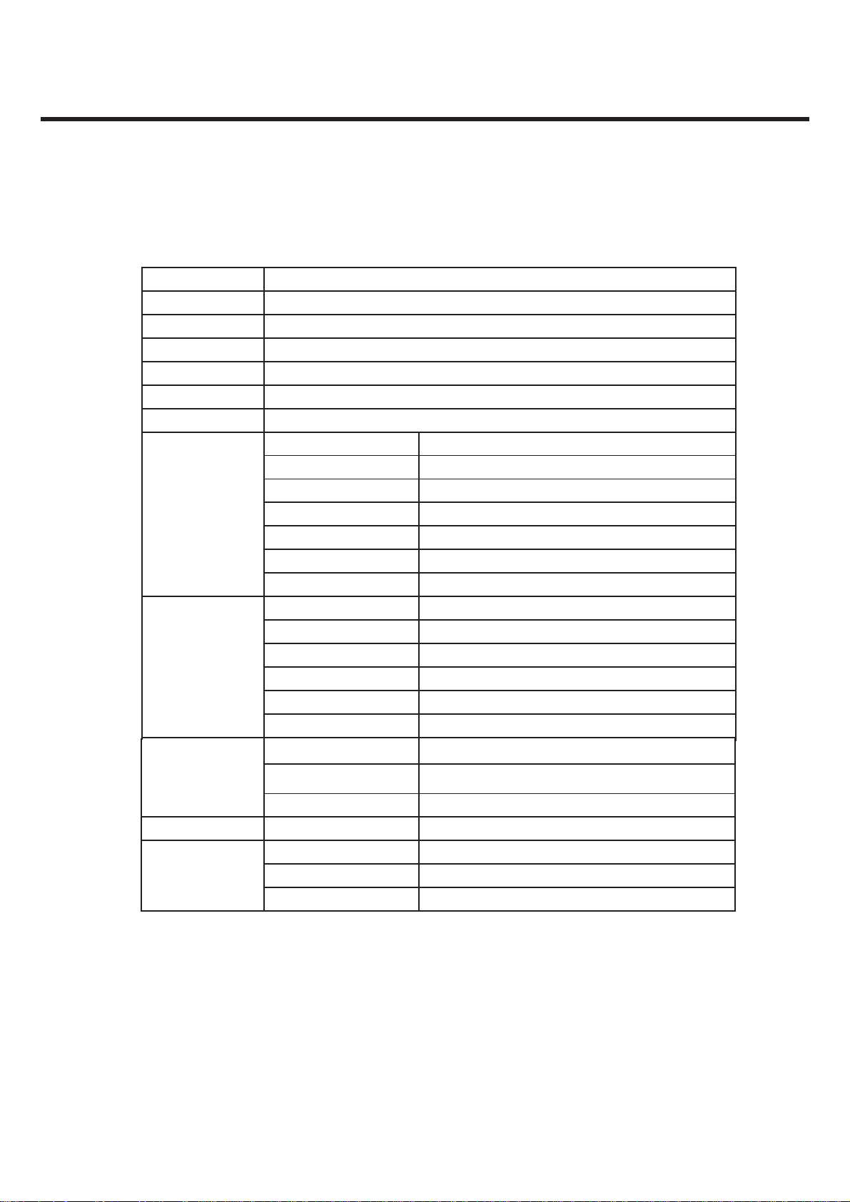
2.1 System Overview
7. LCD
8. Main Camera
(3M)
Type /
Spec.
Bar Type1. Phone Type
109.8 x 56.5 x 11.9 (mm)2. Size
106g3. Weight
1000mAh (Li-Ion)4. Power
MSM7200A, RTR6285, PM75405. MSM Chipset
4Gb(Flash) / 2Gb(SDRAM) /User Memory : 100 MB(TBD)6. Memory
Size
Color
Display Type
NTSC
Contrast Ratio
Type
Resolution
Digital Zoom
ling Down
Video
2. PERFORMANCE
3 inch
400 x 240Dot
262,000
a-Si TFT, Trans missive
Min. 65%, Typ. 70%
Typ. 400:1
0.162mmPixel Pitch
CMOS image sensor
2592(H) X 1944(V) pixels. WQVGA
30 fps at Preview modeFrame Rate
Progressive, <=X2
SXGA, VGA, QVGA, CIF, QCIFImage Sca
400x240 / 176x144,
9. Audi
o
10. Bluetooth
11. WLAN
Throughput
Copyright © 2009 LG Electronics. Inc. All right reserved.
Only for training and service purposes
72poly, SW MIDI1) MIDI
18x12 oval type speaker2) Mono
Speaker/Receiver 3) Receiver
1m
IEEE 802.11b/
4Mbps
50 ~ 200m
- 7 -
g
LGE Internal Use Only
2. PERFORMANCE
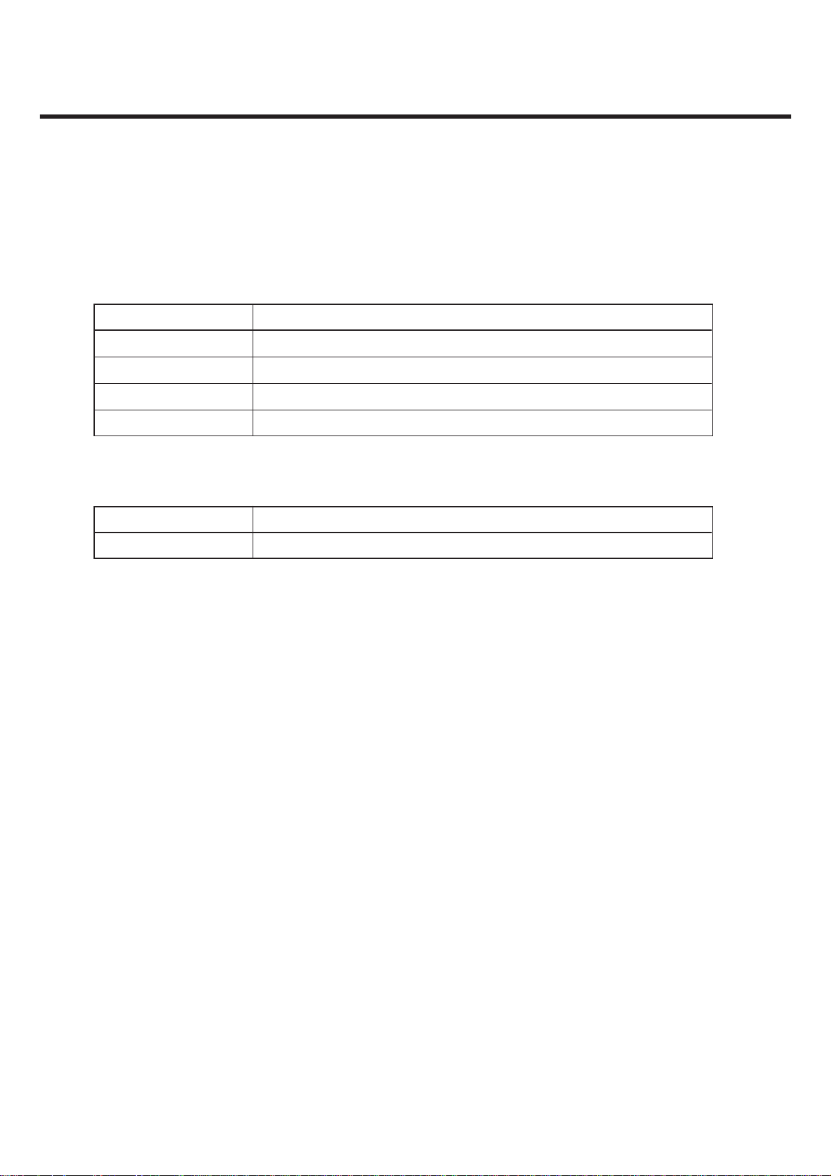
2.2 Usable environment
1) Environment
2) Environment (Accessory)
Item Specification
Voltage 3.7 (Typ), 4.2 (Max)V
Operation Temp -20 ~ +60°C
Storage Temp -30 ~ +85°C
Humidity 65 % (Max)
Reference Spec.
TA Power AC 110 ~ 240V, 60Hz
LGE Internal Use Only Copyright © 2009 LG Electronics. Inc. All right reserved.
- 8 -
Only for training and service purposes

2. PERFORMANCE
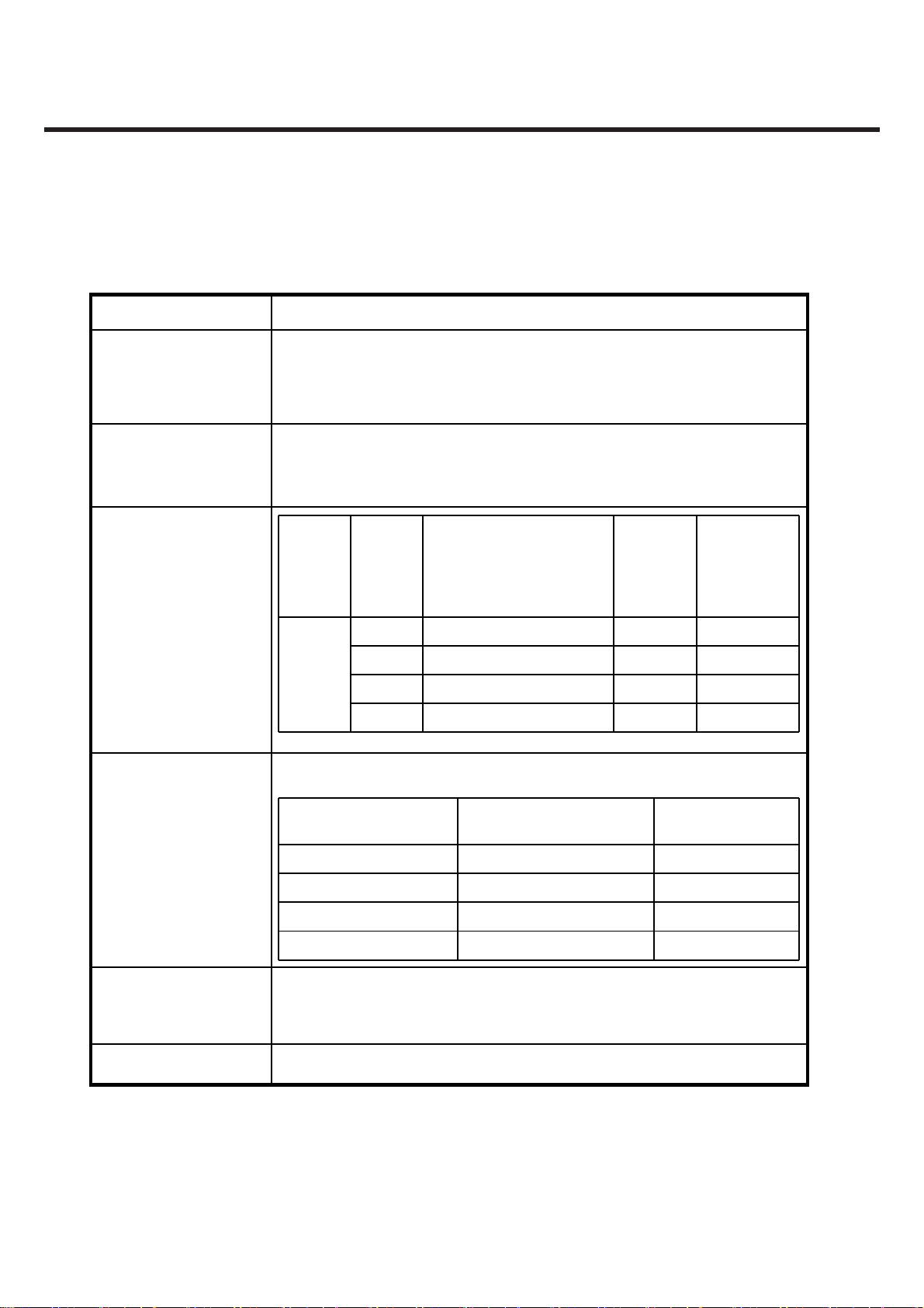
2.3 Radio Performance
1) Transmitter - GSM Mode
SpecificationItem
Phase Error
Frequency Error
EMC(Radiated Spurious Emission
Disturbance)
Transmitter Output power and Burst
Timing
Spectrum due to modulation out to less
than 1800kHz offset
Spectrum due to modulation out to larger
than 1800kHz offset to the edge of the
transmit band
Spectrum due to switching transient
RMS : 5
Peak : 20
GSM : 0.1 ppm
DCS/PCS : 0.1 ppm
GSM/DCS : < -28dBm
GSM : 5dBm – 33dBm 3dB
DCS/PCS : 0dBm – 30dBm 3dB
<3.69usBurst Timing
200kHz : -36dBm
600kHz : -51dBm/-56dBm
GSM :
1800-3000kHz :< -63dBc(-46dBm)
3000kHz-6000kHz : <-65dBc(-46dBm)
6000kHz < : < -71dBc(-46dBm)
DCS :
1800-3000kHz :< -65dBc(-51dBm)
6000kHz < : < -73dBc(-51dBm)
400kHz : -19dBm/-22dBm(5/0), -23dBm
600kHz : -21dBm/-24dBm(5/0), -26dBm
Class II(RBER) : -105dBm(2.439%)Reference Sensitivity – TCH/FS
Intermodulation rejection – Speech
channels
AM Suppression
-GSM : -31dBm - DCS : -29dBm
Copyright © 2009 LG Electronics. Inc. All right reserved.
Only for training and service purposes
0.012(-15 - -40dBm)Usable receiver input level range
800kHz, 1600kHz
: -98dBm/-96dBm (2.439%)
-98dBm/-96dBm (2.439%)
0.5TTiming Advance
- 9 -
LGE Internal Use Only

2. PERFORMANCE
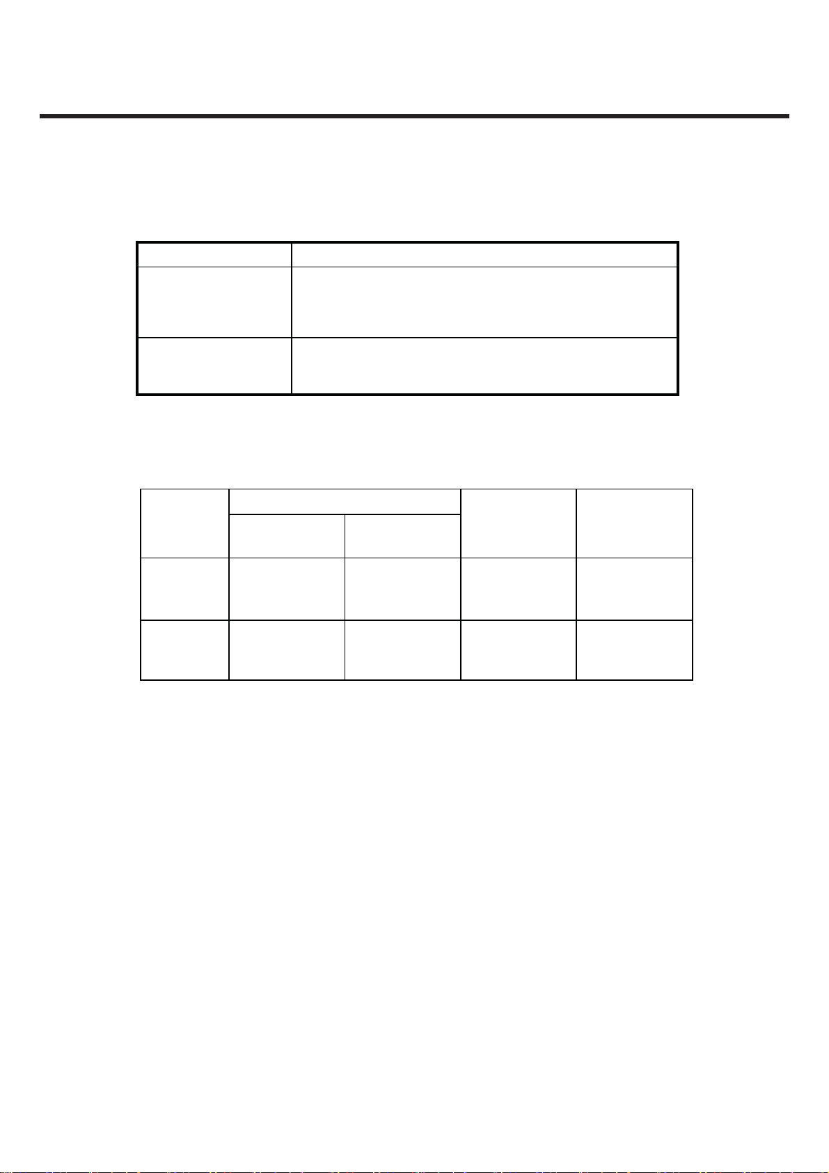
2) Transmitter - WCDMA Mode
SpecificationItem
Transmit Frequency
Maximum Output
Power
Open Loop Power
Control
Minimum Transmit
Power
Occupied Bandwidth
Adjacent Channel
Leakage
Power Ratio (ACLR)
Spurious Emissions
|f-f
| > 12.5 MHz
c
WCDMA850 : 824 MHz ~ 849 MHz
WCDMA900 : 880 MHz ~ 915MHz
WCDMA1900 : 1850 ~1910 MHz
WCDMA2100 : 1920 MHz ~ 1980 MHz
+24 dBm / 3.84 MHz, +1 / -3 dB
within 0.1 PPMFrequency Error
Normal Conditions : within 9 dB,
Extreme Conditions : within 12 dB
< -50 dBm /3.84 MHz
< 5 MHz at 3.84 Mcps (99% of power)
> 33 dB @ 5 MHz,
> 43 dB @ 10 MHz
< -36 dBm / 1 kHz RW @ 9 kHz ≤ f < 150 kHz
< -36 dBm / 10 kHz RW @ 150 KHz ≤ f < 30 MHz
< -36 dBm / 100 kHz RW @ 30 MHz ≤ f < 1 GHz
< -30 dBm / 1 MHz RW @ 1 GHz ≤ f < 12.75 GHz
< -41 dBm / 300 kHz RW @ 1893.5 MHz < f < 1919.6 MHz
< -67 dBm / 100 kHz RW @ 925 MHz ≤ f ≤ 935 MHz
< -79 dBm / 100 kHz RW @ 935 MHz < f ≤ 960 GHz
< -71 dBm / 100 kHz RW @ 1805 MHz ≤ f ≤ 1880 MHz
Transmit
Intermodulation
Peak Code Domain
Error
LGE Internal Use Only Copyright © 2009 LG Electronics. Inc. All right reserved.
< -31 dBc @ 5 MHz & < -41 dBc @ 10 MHz
when Interference CW Signal Level = -40 dBc
< 17.5 %, when Pout ≥ -20 dBmError Vector Magnit u de
< -15 dB at Pout t -20 dBm
- 10 -
Only for training and service purposes

2. PERFORMANCE
3) Receiver - WCDMA Mode
SpecificationItem
Receive Frequency
Adjacent Channel
Selectivity (ACS)
Blocking Characteristic
Intermodulation
Spurious Emissions
WCDMA850 : 849 MHz ~ 894 MHz
WCDMA900 : 925MHz ~ 960 MHz
WCDMA1900 : 1930 ~1990 MHz
WCDMA2100 : 2110 ~ 2170 MHz
BER < 0.001 when Î
BER < 0.001 when Î
ACS > 33 dB where BER < 0.001 when Î
& I
= –52 dBm / 3.84 MHz @ 5 MHz
oac
BER < 0.001 when Î
& I
or I
= -56 dBm / 3.84 MHz @ Fuw(offset) = 10 MHz
blocking
= -44 dBm / 3.84 MHz @ Fuw(offset) = 15 MHz
blocking
BER < 0.001 when Î
BER < 0.001 when Î
& I
= -46 dBm @ F
ouw1
= -46 dBm / 3.84 MHz @ F
& I
ouw2
= -106.7 dBm / 3.84 MHzReference Sensitivity Level
or
= -25 dBm / 3.84 MHz Maximum Input Level
or
= -92.7 dBm / 3.84 MHz
or
= -103.7 dBm / 3.84 MHz
or
= -103.7 dBm / 3.84 MHz & I
or
= -103.7 dBm / 3.84 MHz
or
(offset) = 10 MHz
uw1
(offset) = 20 MHz
uw2
< -57 dBm / 100 kHz BW @ 9 kHz ≤ f < 1 GHz
< -47 dBm / 1 MHz BW @ 1 GHz ≤ f ≤ 12.75 GHz
blocking
= -44 dBmSpurious Response
Inner Loop Power Control
In Uplink
Copyright © 2009 LG Electronics. Inc. All right reserved.
Only for training and service purposes
Adjust output(TPC command)
cmd 1dB 2dB 3dB
+1 +0.5/1.5 +1/3 +1.5/4
0 -0.5/+0.5 -0.5/+0.5 -0.5/+0.5
-1 -0.5/-1.5 -1/-3 -1.5/-4
group(10equal command group)
+1 +8/+12 +16/+24
- 11 -
LGE Internal Use Only
2. PERFORMANCE
4) Transmitter - HSDPA Mode
SpecificationItem
Transmit Frequency
Maximum Output
Power
HS-DPCCH
824 MHz ~ 849 MHz
880 MHz ~ 915 MHz
1850MHz ~ 1910 MHz
1920 MHz ~ 1980 MHz
Sub-Test
1=1/15, 2=12/15 21~25dBm / 3.84 MHz
3=13/15 4=15/8 20~25dBm / 3.84 MHz
5=15/7 6=15/0 19~25dBm / 3.84 MHz
Sub-
test in
table
C.10.1.
4
5
Sub-Test : 1=1/15, 2=12/15, 3=13/15, 4=15/8, 5=15/7, 6=15/0
Power
step
Power step slot boundary
Power
step size,
P [dB]
Transmitter
power step
tolerance
[dB]
+/- 2.36Start of Ack/Nack1
+/- 0.61Start of CQI2
+/- 0.60Middle of CQI3
+/- 2.35End of CQI4
Frequency offset from
carrier △f
Spectrum Emission
Mask
Adjacent Channel
Leakage
Power Ratio (ACLR)
LGE Internal Use Only Copyright © 2009 LG Electronics. Inc. All right reserved.
Sub-Test : 1=1/15, 2=12/15, 3=13/15, 4=15/8, 5=15/7, 6=15/0
> 33 dB @ 5 MHz
> 43 dB @ 10 MHz
3GPP Not CompleteError Vector Magnit u de
- 12 -
Minimum requirement
Only for training and service purposes
Measurement
Bandwidth
30 kHz-35-15×(△f-2.5)dBc2.5 ~ 3.5 MHz
1 MHz-35-1×(△f-3.5)dBc3.5 ~ 7.5 MHz
1 MHz-35-10×(△f-7.5)dBc7.5 ~ 8.5 MHz
1 MHz-49dBc8.5 ~ 12.5 MHz
5)Receiver - HSDPA Mode
2.4 Current Consumption
1) Current Consumption
(Stand by and Voice Call Test Condition : Bluetooth off, LCD backlight off,Neighbor Cell off) (VT Test
Condition : Speaker off, LCD backlight On)
No Item Specification
1 Receive Frequency 849 MHz ~ 894 MHz
1930 MHz ~1990 MHz
2110 ~ 2170 MHz
2 Maximum Input Level Sub-Test : 1=1/15, 2=12/15, 3=13/15, 4=15/8, 5=15/7, 6=15/0
(BLER or R), 16QAM Only BLER < 10% or R >= 700kbps
Stand by Voice Call VT
Bluetooth Bluetooth
Off Connected
WCDMA
Under 3.00 mA Under 4.50 mA Under 250 mA N/A
(DRX=1.28) (DRX=1.28) (TX=12dBm low)
GSM Under 3.00 mA Under 4.50 mA Under 350 mA
Paging=5 period Paging=5 period (TX Power Level 5)
Receive Frequency
Maximum Input Level
(BLER or R), 16QAM Only
2. PERFORMANCE
SpecificationItem
849 MHz ~ 894 MHz
925 MHz ~ 960 MHz
1930 MHz ~1990 MHz
2110 ~ 2170 MHz
Sub-Test : 1=1/15, 2=12/15, 3=13/15, 4=15/8, 5=15/7, 6=15/0
BLER < 10% or R >= 700kbps
Copyright © 2009 LG Electronics. Inc. All right reserved.
Only for training and service purposes
- 13 -
LGE Internal Use Only
2. PERFORMANCE
2.5 RSSI BAR
2.6 Battery BAR
Indication Standby
Bar 4 → 3 72%
Bar 3 → 2 47%
Bar 2 → 1 25%
Bar 1 → 05%
Low Battery Alarm 15%
Critical Low Battery Alarm 5%
POWER OFF 0%
Level Change WCDMA GSM
BAR 4 → 3-82 ± 2 dBm -91 ± 2 dBm
BAR 3 → 2-92 ± 2 dBm -96 ± 2 dBm
BAR 2 → 1 -102 ± 2 dBm -101 ± 2 dBm
BAR 1 → 0 -112 ± 2 dBm -106 ± 2 dBm
LGE Internal Use Only Copyright © 2009 LG Electronics. Inc. All right reserved.
- 14 -
Only for training and service purposes
3. TECHNICAL BRIEF
3. TECHNICAL BRIEF
3.1. GENERAL DESCRIPTION
The GM730 supports UMTS-900(Band VIII), UMTS-1900(Band II), UMTS-2100(Band I), GSM-850, GSM-900,
GSM-1800, and GSM-1900 based GSM/GPRS/EDGE/UMTS. All receivers and the UMTS transmitter use the
radioOne1Zero-IF architecture to eliminate intermediate frequencies, directly converting signals between RF
and baseband. The quad-band GSM transmitters use a baseband-to-IF up-conversion followed by an offset
phase-locked loop that translates the GMSK-modulated or 8-PSK-modulated signal to RF.
TCXO
SBDT
RF_ON
TX_IQ
PRX_IQ
DRX_IQ
DAC_IREF
VCTCXO
19.2MHz
VCONT
GPS_LNA_EN
WCDMA_900_ON
WCDMA_1900_ON
WCDMA_2100_ON
TCXO_EN
TRK_LO_ADJ
TCXO
PMIC_SSBI
PA_POWER_CTL
PA_RANGE0
SSBDT_RTR
TX_ON
MSM7200A
GPIO58
GPIO22
GPIO110
PA_ON0
TX_IQ
PRX_IQ
DRX_IQ
DAC_IREF
ANT_SEL0/1/2/3
VBATT
VAPC
FRONT
END
MODULE
SKY77521
LB_RF_IN
HB_RF_IN
CTRL0/1/2/3
GSM_PA_RAMP
WCDMA2100
DIVERSITY
RX4
RX3
RX2
RX1
W900
Duplexer
W2100
Duplexer
W1900
Duplexer
+VPWR
49.9R
Coupler
O
O
T
T
Coupler
T
T
O
O
Coupler
O
O
T
T
RX SAW
FILTER
RX SAW
FILTER
RX SAW
FILTER
RX SAW
FILTER
RX SAW
FILTER
I
I
C
C
C
C
I
I
I
I
C
C
G850/900
DCS/PCS
LNA
WCDMA_900_ON
WCDMA_2100_ON
VMODE1
WCDMA
Dual PAM
VMODE2
VMODE2
W1900
PAM
VMODE1
WCDMA_1900_ON
GSM850
EGSM900
DCS1800
PCS1900
GPS_LNA_EN
RX SAW
FILTER
WCDMA900 TX
TX SAW
FILTER
WCDMA2100 TX
TX SAW
FILTER
WCDMA1900 TX
TX SAW
FILTER
RX SAW
FILTER
PM7540
SBDT_SSBI
GPS_IN
WB_MX_INP
WB_MX_INM
WPRXSE2_OUT
WPRXSE2
WPRXLBP
WPRXLBN
LB_RF_OUT2
HB_RF_OUT3
HB_RF_OUT2
PDET_IN
WPRXHBP
WPRXHBN
WDRXHB2
LB_RF_OUT1
HB_RF_OUT1
GCELL_INP
GCELL_INP
GCELL_INN
GCELL_INN
EGSM_INP
EGSM_INP
EGSM_INN
EGSM_INN
DCS_INP
DCS_INP
DCS_INN
DCS_INN
GPCS_INP
GPCS_INP
GPCS_INP
GPCS_INN
GPCS_INN
GPCS_INN
PMIC_TCXO
RTR6285
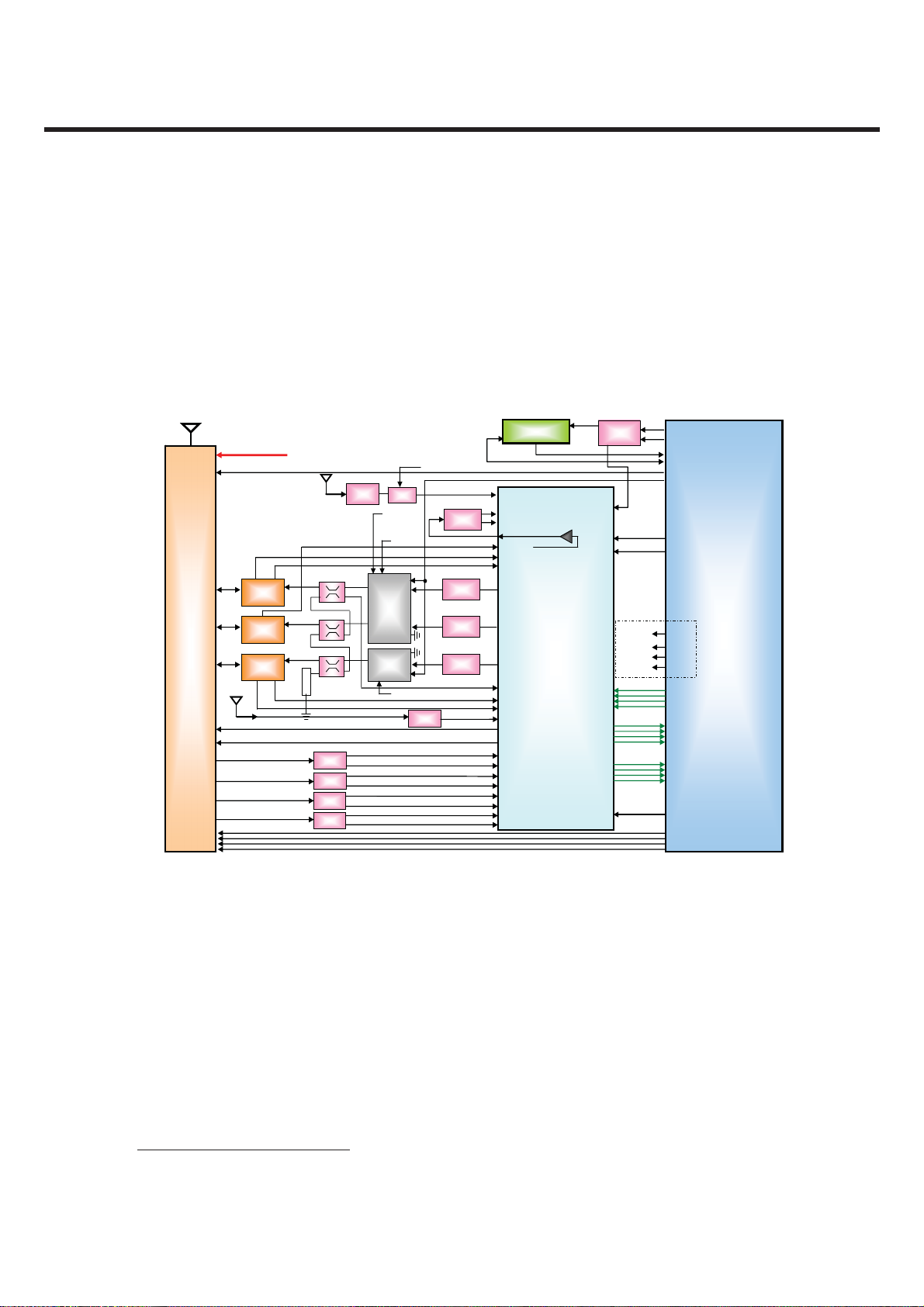
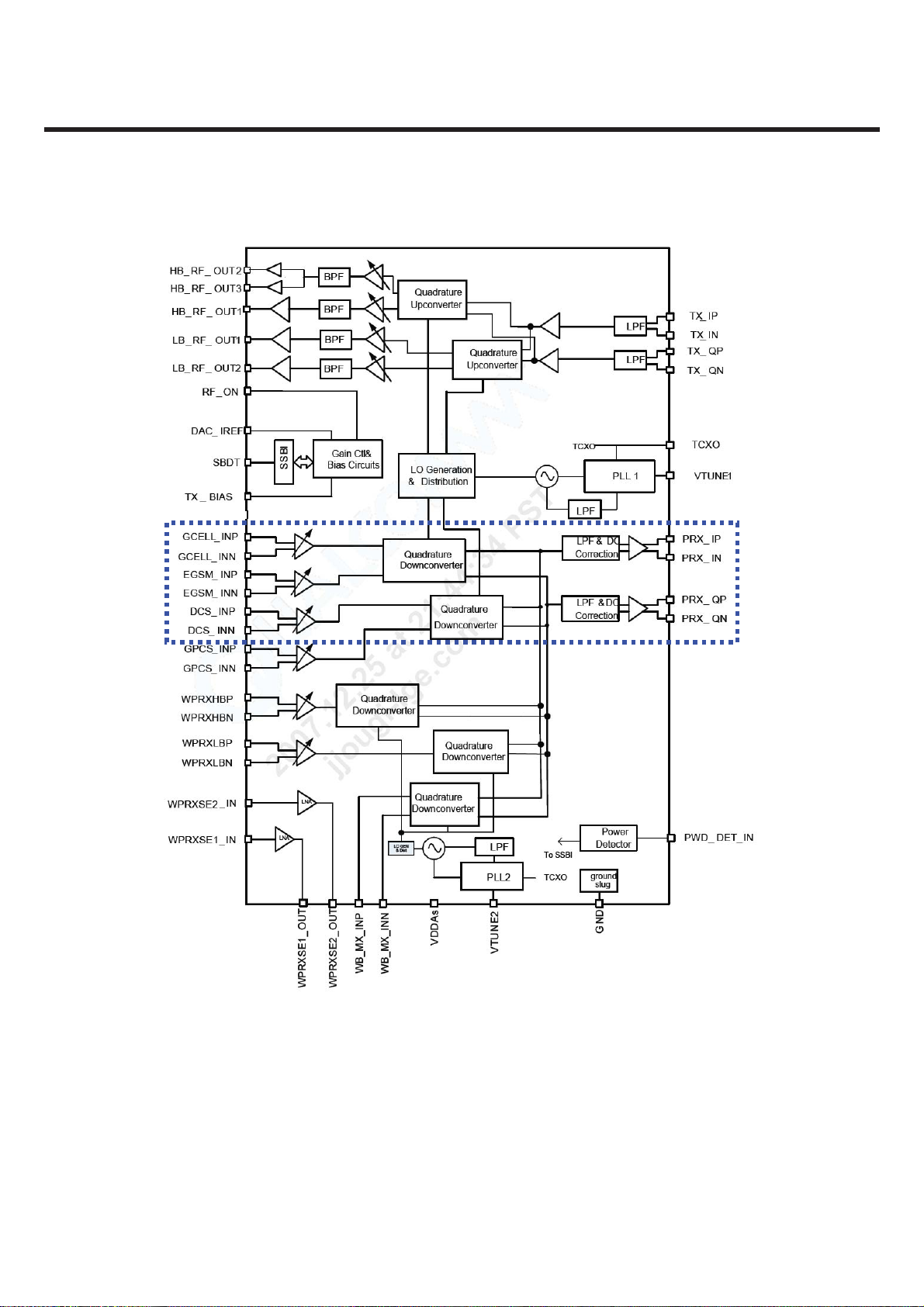
[Figure 1-1] Block diagram of RF part
A generic, high-level functional block diagram of GM730 is shown in Figure 1-1. One antenna collects base
station forward link signals and radiates handset reverse link signals. The antenna connects with receive and
transmit paths through a SKY77521 (FEM, Front End Module + GSM PAM). The UMTS receive paths each
include an LNA, an RF band-pass filter, and a downconverter that translate the signal directly from RF-tobaseband using radioOne ZIF techniques. The RFIC’s RX analog baseband outputs, for the receive chains,
connect to the MSM IC. The UMTS and GSM RX baseband outputs share the same inputs to the MSM IC.
For the transmit chains, the RTR6285 IC directly translates the TX baseband signals (from
the MSM device) to an RF signal using an internal LO generated by integrated on-chip PLL
and VCO. The RTR6285 IC outputs deliver fairly high-level RF signals that are first filtered by
TX SAWs and then amplified by their respective UMTS PAs.
1
QUALCOMM’s branded chipset that implements a Zero-IF radio architecture.
Copyright © 2009 LG Electronics. Inc. All right reserved.
- 15 -
Only for training and service purposes
LGE Internal Use Only
3. TECHNICAL BRIEF
In the GSM receive path, the received RF signals are applied through their band-pass filters and downconverted directly to baseband in the RTR6285 transceiver IC. These baseband outputs are shared with the
UMTS receiver and routed to the MSM IC for further signal processing.
The GSM/EDGE transmit path employs one stage of up-conversion and, in order to improve efficiency, is
divided into phase and amplitude components to produce an open-loop Polar topology:
1. The on-chip quadrature up-converter translates the GMSK-modulated signal or 8-PSK modulated signal, to
a constant envelope phase signal at RF;
2. The amplitude-modulated (AM) component is applied to the ramping control pin of Polar power amplifier
from a DAC within the MSM
GM730 power supply voltages are managed and regulated by the PM7540 Power Management IC. This
versatile device integrates all wireless handset power management, general housekeeping, and user
interface support functions into a single mixed signal IC. It monitors and controls the external power source
and coordinates battery recharging while maintaining the handset supply voltages using low dropout,
programmable regulators.
The device’s general housekeeping functions include an ADC and analog multiplexer circuit for monitoring
on-chip voltage sources, charging status, and current flow, as well as user-defined off-chip variables such as
temperature, RF output power, and battery ID. Various oscillator, clock, and counter circuits support IC and
higher-level handset functions. Key parameters such as under-voltage lockout and crystal oscillator signal
presence are monitored to protect against detrimental conditions.
3.2. GSM MODE
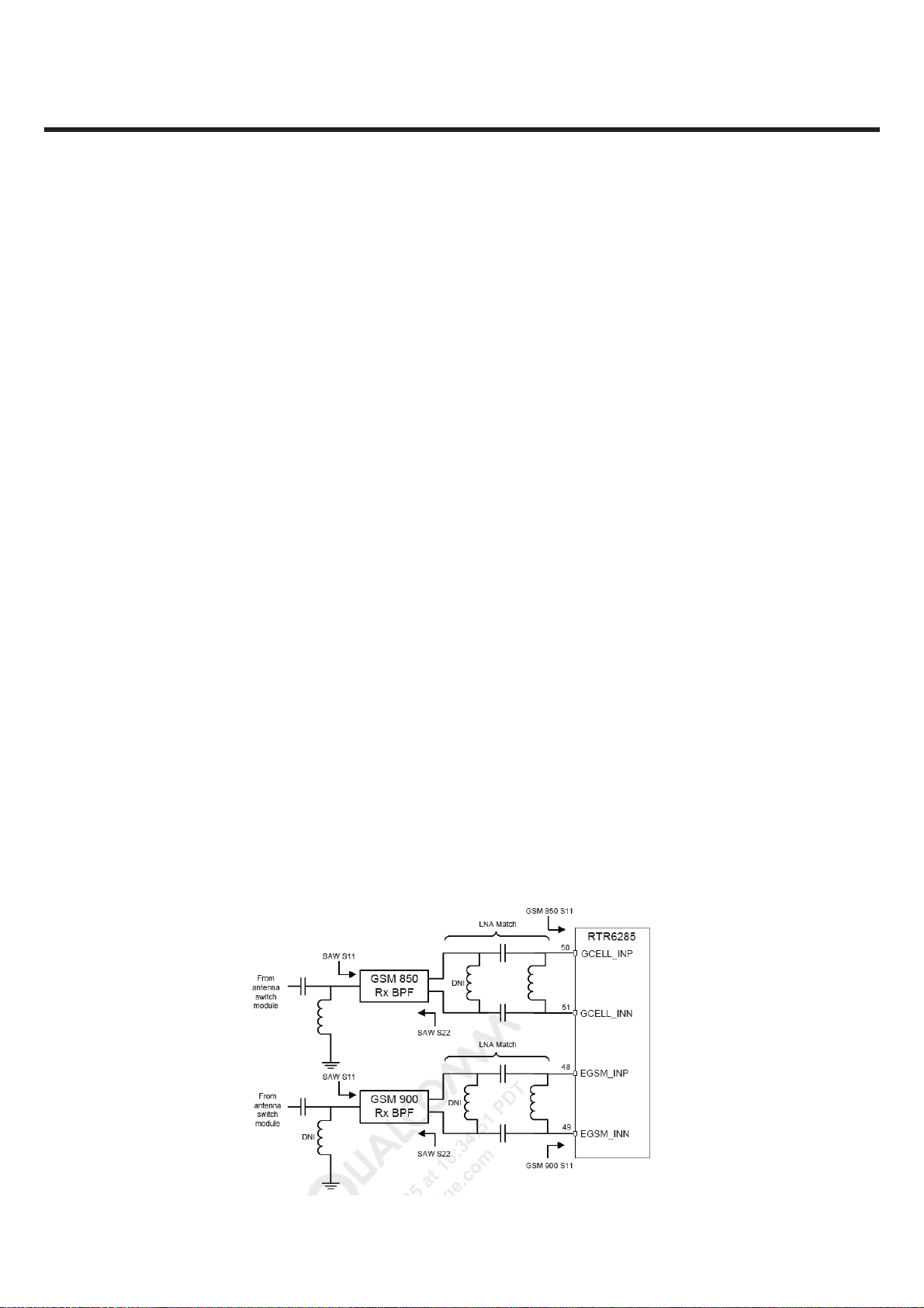
3.2.1 GSM RECEIVER
The GSM-850, GSM-900, GSM-1800, and GSM-1900 receiver inputs of RTR6285 are connected to the
transceiver front-end circuits(switch module) through saw filters. GSM-850, GSM-900, GSM-1800, and GSM1900 receiver inputs use differential configurations to improve common-mode rejection and second-order
non-linearity performance as shown in Figure 1-2. The balance between the complementary signals is critical
and must be maintained from the RF filter outputs all the way into the IC pins
LGE Internal Use Only Copyright © 2009 LG Electronics. Inc. All right reserved.
- 16 -
Only for training and service purposes
3. TECHNICAL BRIEF
[Figure 1-2] GSM Receiver Inputs Topologies
Since GSM-850, GSM-900, GSM-1800, and GSM-1900 signals are time-division duplex (the handset can only
receive or transmit at one time), switches are used to separate RX and TX signals in place of frequency
duplexers – this is accomplished in the switch module. The GSM-850, GSM-900, GSM-1800, and GSM-1900
receive signals are routed to the RTR6285 through saw filters and matching networks that transform singleended 50-Ω sources to differential impedances optimized for gain and noise figure. The RTR input uses a
differential configuration to improve second-order inter-modulation and common mode rejection
performance. The RTR6285 input stages include MSM-controlled gain adjustments that maximize receiver
dynamic range.
The amplifier outputs drive the RF ports of the quadrature RF-to-baseband downconverters. The
downconverted baseband outputs are multiplexed and routed to lowpass filters (one I and one Q) having
passband and stopband characteristics suitable for GMSK or 8-PSK processing. These filter circuits include DC
offset corrections. The filter outputs are buffered and passed on to the MSM7200A IC for further processing as
shown in Figure 1-3.
Copyright © 2009 LG Electronics. Inc. All right reserved.
Only for training and service purposes
- 17 -
LGE Internal Use Only
3. TECHNICAL BRIEF
[Figure 1-3] RTR6285 RX feature
LGE Internal Use Only Copyright © 2009 LG Electronics. Inc. All right reserved.
- 18 -
Only for training and service purposes
3. TECHNICAL BRIEF
3.2.2 GSM TRANSMITTER
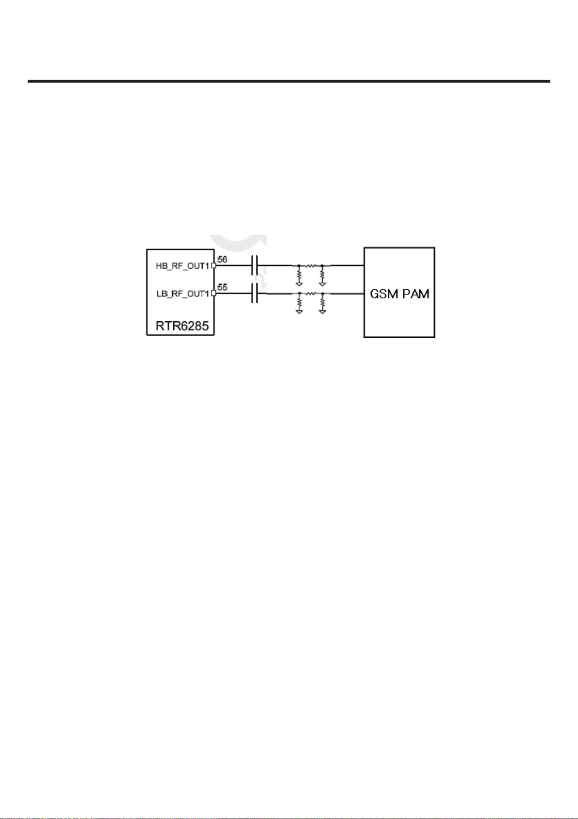
The RTR6285 transmitter outputs(HB_RF_OUT1 and LB_RF_OUT1) include on-chip output matching
inductors. 50ohm output impedance is achieved by adding a series capacitor at the output pins. The
capacitor value may be optimized for specific applications and PCB characteristics based on pass-band
symmetry about the band center frequency as shown in Figure 1-3.
[Figure 1-4] GSM Transmitter Outputs Topologies
The RTR6285 IC is able to support GSM850/GSM 900 and GSM 1800/1900 mode transmitting. This design
guideline shows a quad-band GSM application. Both high-band and low band outputs are followed by
resistive pads to ensure that the load presented to the outputs remains close to 50ohm.
Copyright © 2009 LG Electronics. Inc. All right reserved.
Only for training and service purposes
- 19 -
LGE Internal Use Only
3. TECHNICAL BRIEF
3.3. UMTS MODE
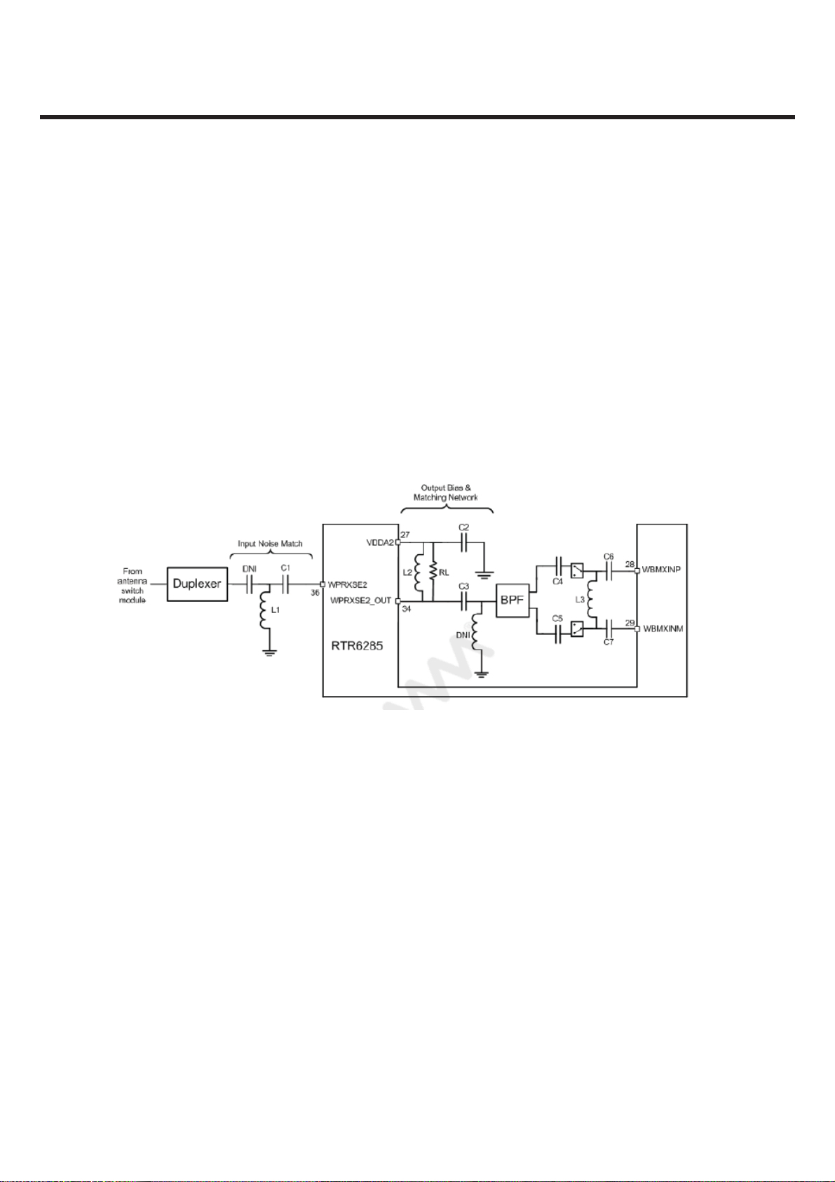
3.3.1 UMTS RECEIVER
The UMTS duplexer receiver output is routed to LNA circuits within the RTR6285 device as shown in Figure 1-
5. The UMTS RX input is provided with an on-chip LNA that amplifies the signal before a second stage filter
that provides differential downconverter as shown in Figure 1-5. This second stage input is configured
differentially to optimize second-order intermodulation and common mode rejection performance. The gain
of the UMTS front end amplifier and the UMTS second stage differential amplifier are adjustable, under MSM
control, to extend the dynamic range of the receivers. The second stage UMTS RX amplifiers drive the RF
ports of the quadrature RF-to-baseband downconverters. The downconverted UMTS RX baseband outputs
are routed to lowpass filters having passband and stopband characteristics suitable for UMTS RX processing.
These filter circuits allow DC offset corrections, and their differential outputs are buffered to interface shared
with GSM RX to the MSM IC. The UMTS baseband outputs are turned off when the RTR6285 is
downconverting GSM signals and on when the UMTS is operating.
[Figure 1-5] UMTS Receiver Inputs Topologies
LGE Internal Use Only Copyright © 2009 LG Electronics. Inc. All right reserved.
- 20 -
Only for training and service purposes

3. TECHNICAL BRIEF
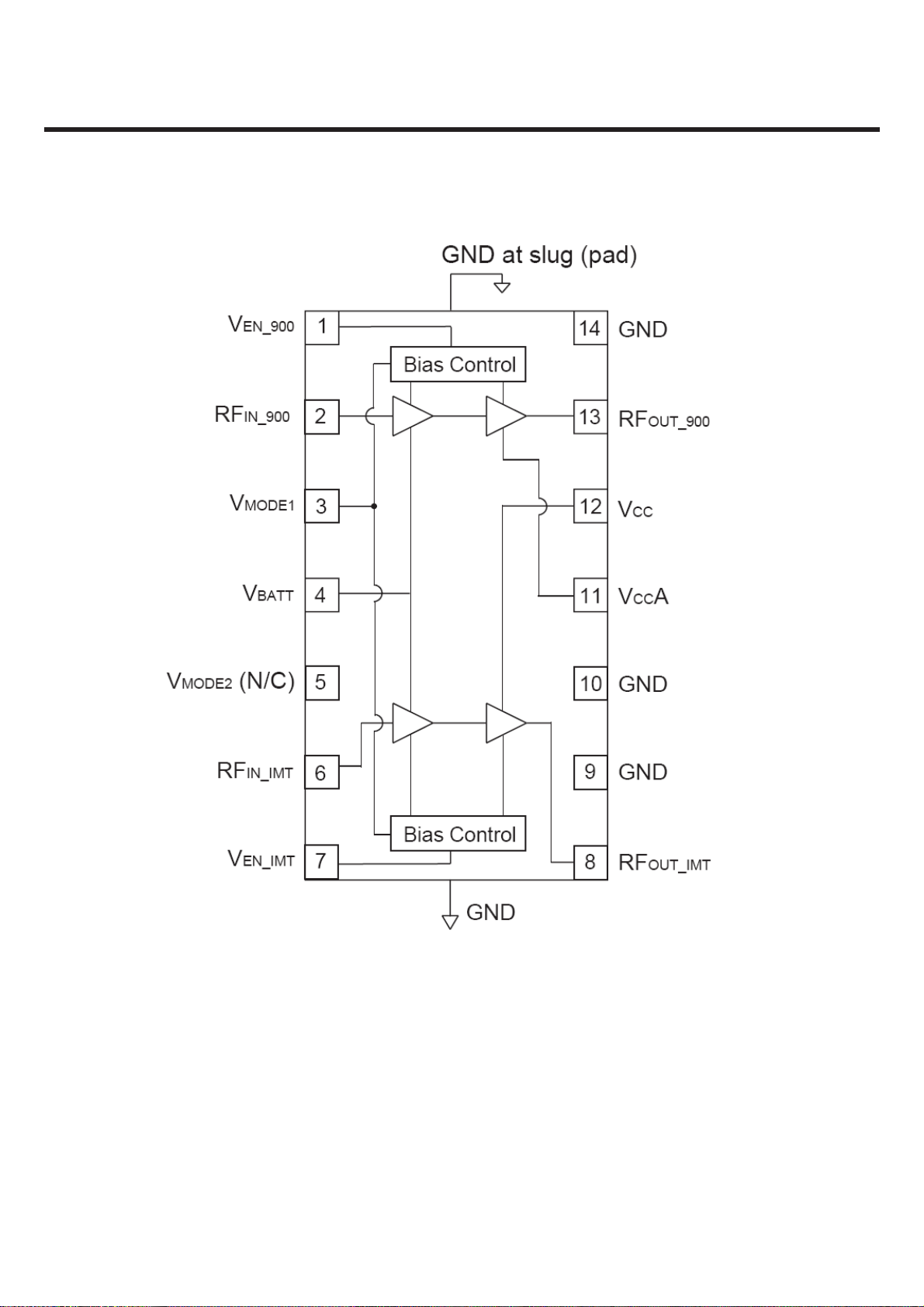
3.3.2 UMTS TRANSMITTER
The UMTS TX path begins with differential baseband signals (I and Q) from the MSM device.
These analog input signals are amplified, filtered, and applied to the quadrature up-converter mixers. The upconverter output is amplified by multiple variable gain stages that provide transmit AGC control. The AGC
output is filtered and applied to the driver amplifier; this output stage includes an integrated matching
inductor that simplifies the external matching network to a single series capacitor to achieve the desired 50Ω interface.
The RTR6285 UMTS output is routed to its power amplifier through a bandpass filter, and delivers fairly highlevel signals that are filtered and applied to the PA. Transmit power is delivered from the duplexer to the
antenna through the switch module.
The transceiver LO synthesizer is contained within the RTR6285 IC with the exception of the off-chip loop
filter components and the VC-TCXO. This provides a simplified design for multimode applications. The PLL
circuits include a reference divider, phase detector, charge pump, feedback divider, and digital logic
generator.
UMTS TX Using only PLL1, the LO generation and distribution circuits create the necessary LO signals for nine
different frequency converters. The UMTS transmitter also employs the ZIF architecture to translate the signal
directly from baseband to RF. This requires FLO to equal FRF, and the RTR6285 IC design achieves this without
allowing FVCO to equal FRF.
The RTR6285 IC is able to support UMTS 2100/1900/1800/1700/900 and 850 mode transmitting. This design
guideline shows UMTS 2100, UMTS1900 and UMTS850 applications.
Copyright © 2009 LG Electronics. Inc. All right reserved.
Only for training and service purposes
- 21 -
LGE Internal Use Only
3. TECHNICAL BRIEF
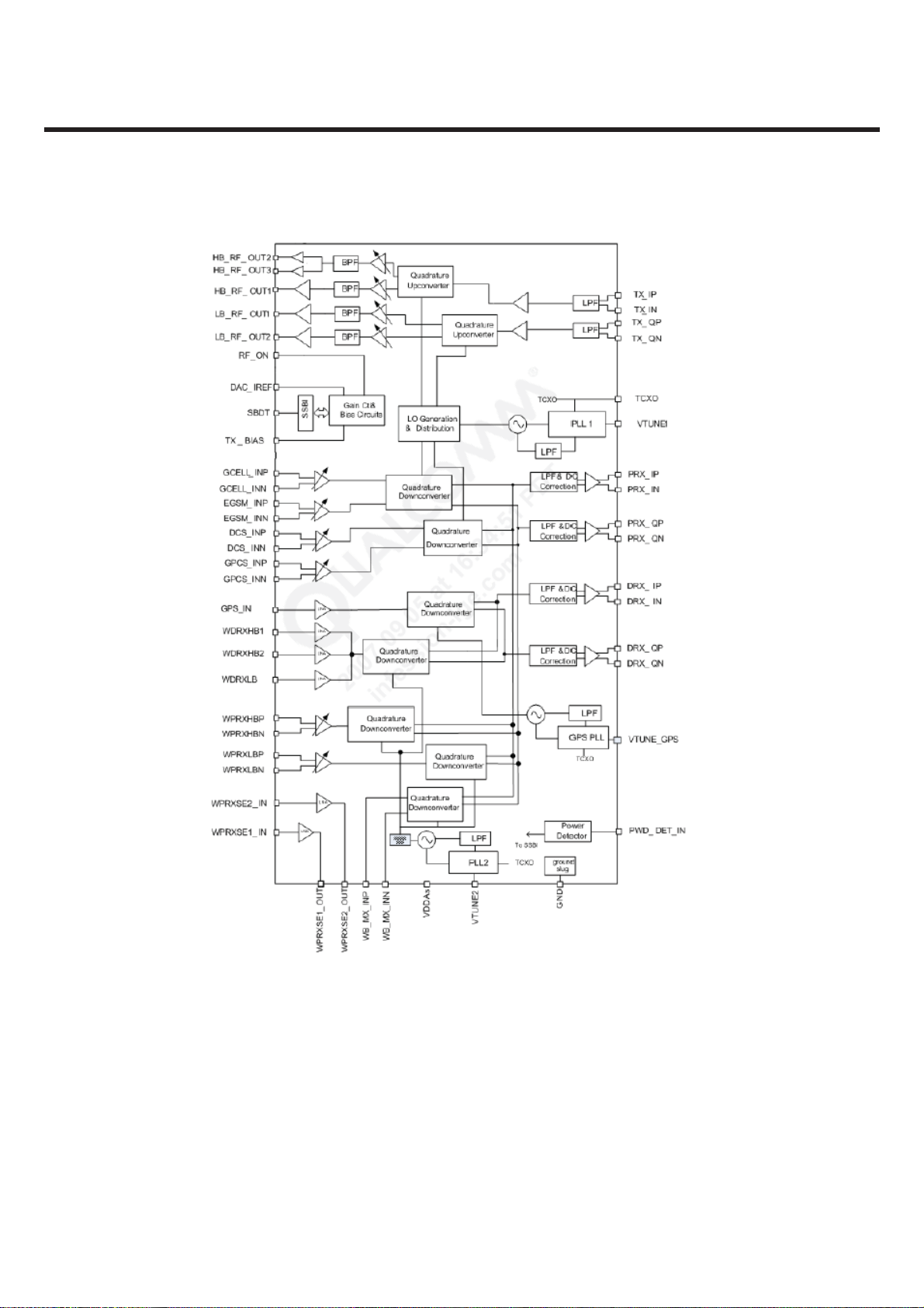
[Figure 1.6] RTR6285 IC Functional Block Diagram
LGE Internal Use Only Copyright © 2009 LG Electronics. Inc. All right reserved.
- 22 -
Only for training and service purposes
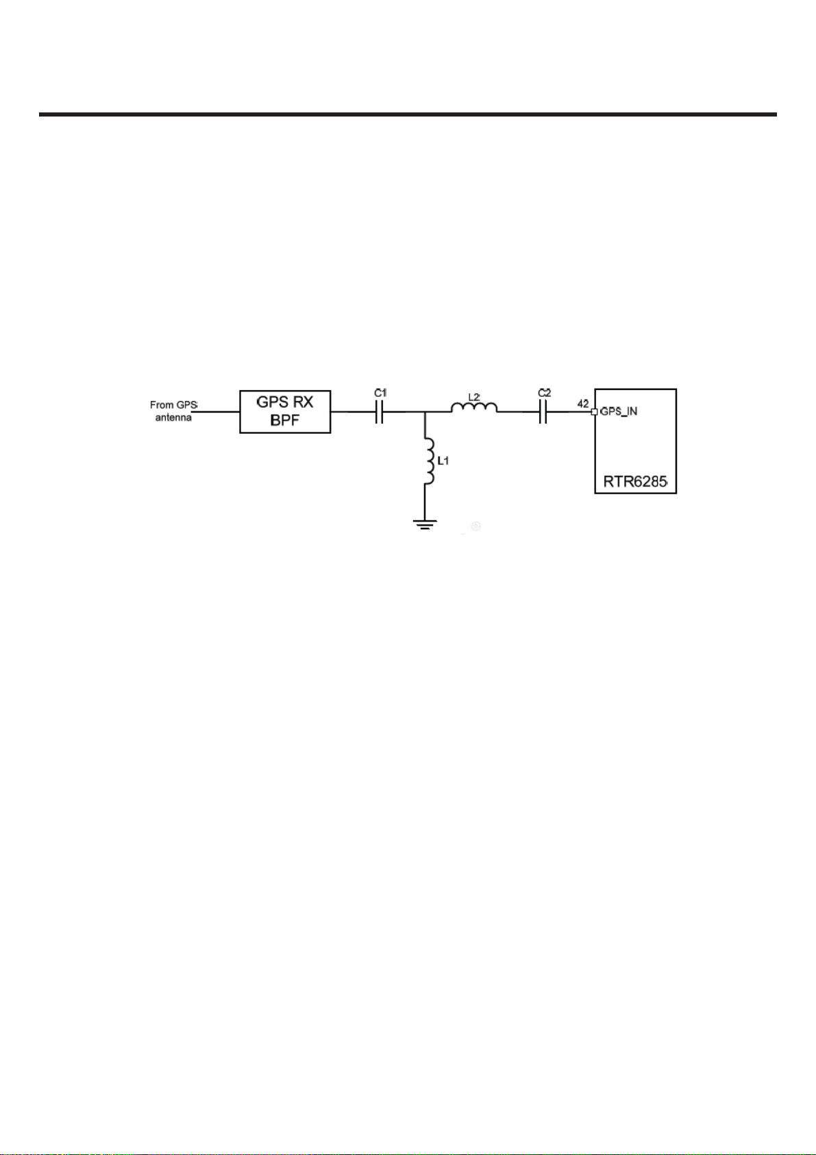
3.4. GPS MODE
3. TECHNICAL BRIEF
3.4.1 GPS RECEIVER
The GPS receiver input employs a single-ended connection realized by this pin. The GPS input is routed from
the GPS antenna switch, through a band-pass filter and then an impedance transformer circuit that optimally
matches the impedance looking into the GPS LNA. The impedance transformer circuit topology is shown in
Figure 1-7.
[Figure 1.7] GPS Input Network Topology
3.5. LO GENERATION and DISTRIBUTION CIRCUIT
The integrated LO generation and distribution circuits are driven by internal VCOs to support various modes
to yield highly flexible quadrature LO outputs that drive all GSM/EDGE, UMTS band and GPS upconverters
and downconverters; with the help of these LO generation and distribution circuits, true zero-IF architecture
is employed in all GSM and UMTS band receivers and transmitters to translate the signal directly from RF-tobaseband and from baseband-to-RF. Two fully functional fraction-N synthesizers, including VCOs and loop
filters, are integrated within the RTR6285 IC. In addition, the RTR6285 has a third synthesizer used for GPS
operation. The first synthesizer (PLL1) in the RTR6285 creates the transceiver Los that support the UMTS
transmitter, and all four GSM band receivers and transmitters including: GSM850, GSM900, GSM1800, and
GSM1900. The second synthesizer (PLL2) in the RTR6285 IC provides the LO for the UMTS primary receiver. For
the RTR6285 IC only, the second synthesizer also provides the LO for the secondary UMTS receiver. The third
synthesizer (PLL3), only in the RTR6285 IC, provides the LO for the GPS receiver. An external TCXO input signal
is required to provide the synthesizer frequency reference to which the PLL is phase and frequency locked.
The RTR6285 ICs integrate most of the PLL loop filter components on-chip except for three off-chip loop
filter-series capacitors, which significantly reduces off-chip component requirement. With the integrated
fractional-N PLL synthesizers, the RTR6285 ICs have the advantage of more flexible loop bandwidth control,
fast lock time, and low-integrated phase error.
Copyright © 2009 LG Electronics. Inc. All right reserved.
Only for training and service purposes
- 23 -
LGE Internal Use Only
3. TECHNICAL BRIEF
3.6. OFF-CHIP RF COMPONENTS
3.6.1 ALM-1412(U108:GPS LNA)
The ALM-1412 is an LNA module, with integrated filter, designed for GPS band applications at 1.575GHz. The
LNA uses AVAGO Technologies’ proprietary GaAs Enhancement-mode pHEMT process to achieve high gain
with very low noise figure and high linearity Noise figure distribution is very tightly controlled. A CMOScompatible shutdown pin is included either for turning the LNA on/off, or for current adjustment. The
integrated filter utilizes an Avago Technologies’ leading edge FBAR filter for exceptional rejection at Cell/PCS
Band frequencies. The ALM-1412 is useable down to 1V operation. It achieves low noise figure, high gain and
linearity even at 1V, making it suitable for use in critical low-power GPS applications or during low-battery
situations.
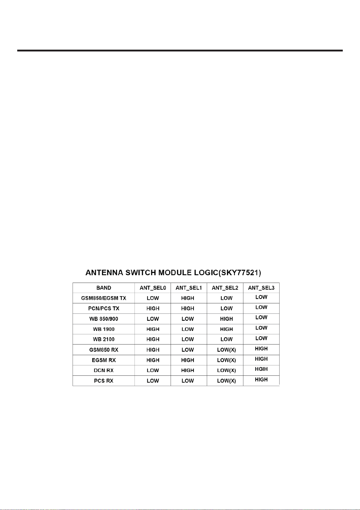
3.6.2 SKY77521(U101:FEM + GSM Quad-Band PAM)
SKY77521 is transmit and receive Front End Module(FEM) designed in a very low profile
(1mm), compact form factor for quad-band cellular handsets comprising GSM850/900,
DCS1800, and PCS1900 operation – a complete transmit VCO-to-Antenna and Antenna-toreceive SAW filter solution. The FEM also supports Class 12 General Packet Radio Service
(GPRS) multi-slot operation and EDGE Polar Modulation. WCDMA switch-through support is
provided by three dedicated high-linearity ports.
[Table 1] Antenna Switch Module Logic
LGE Internal Use Only Copyright © 2009 LG Electronics. Inc. All right reserved.
- 24 -
Only for training and service purposes
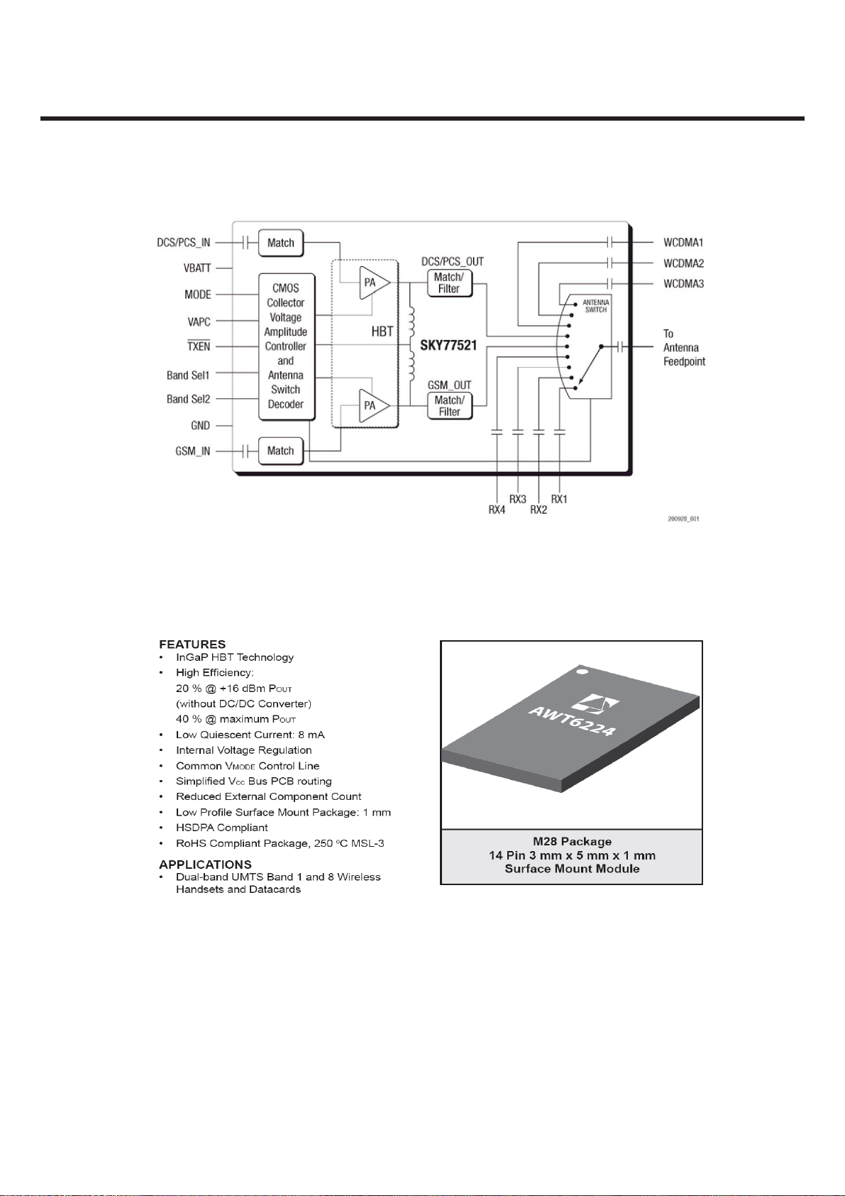
3. TECHNICAL BRIEF
[Figure 1.8] SKY77521 Functional Block Diagram.
3.6.3 W-CDMA Dual-Band POWER AMPLIFIER (U104: AWT6224R)
Copyright © 2009 LG Electronics. Inc. All right reserved.
Only for training and service purposes
- 25 -
LGE Internal Use Only
3. TECHNICAL BRIEF
[Figure 1.9] AWT6224R Functional Block Diagram.
LGE Internal Use Only Copyright © 2009 LG Electronics. Inc. All right reserved.
- 26 -
Only for training and service purposes
3. TECHNICAL BRIEF
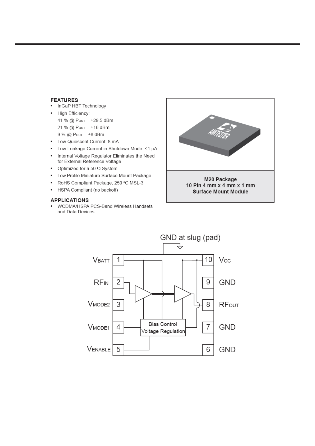
3.6.4 W-CDMA 1900 POWER AMPLIFIER (U107: AWT6278R)
.
[Figure 1.10] AWT6278R Functional Block Diagram.
Copyright © 2009 LG Electronics. Inc. All right reserved.
Only for training and service purposes
- 27 -
LGE Internal Use Only

3. TECHNICAL BRIEF
3.7 Main Features
1. LG GM730 Main Features
- Bar Type Simple & Stylish design
- UMTS 2100 + UMTS1900 + UMTS900+
GSM 900 + DCS 1800 + PCS 1900 + GSM850 based GSM/GPRS/EDGE/UMTS
- HSDPA 3.6Mbps
- 3.0” WQVGA LCD (262K TFT)
- Touch Sensitive User Interface
- 5M AF Camera
- Stereo Headset & Speaker phone
- 72 Poly Sound
- MP3/AAC/AMR/MIDI/3GP/SMAF decoder and play
- MPEG4 encoder/decoder and play/save
- JPEG en/decoder
- Supports Bluetooth and HS-USB
- Supports WLAN
- Internal User Memory over 128MB
- 1000 mAh (Li-Ion Polymer)
- Windows MobileTM6.1 Professional
- Microsoft Office Mobile
LGE Internal Use Only Copyright © 2009 LG Electronics. Inc. All right reserved.
- 28 -
Only for training and service purposes
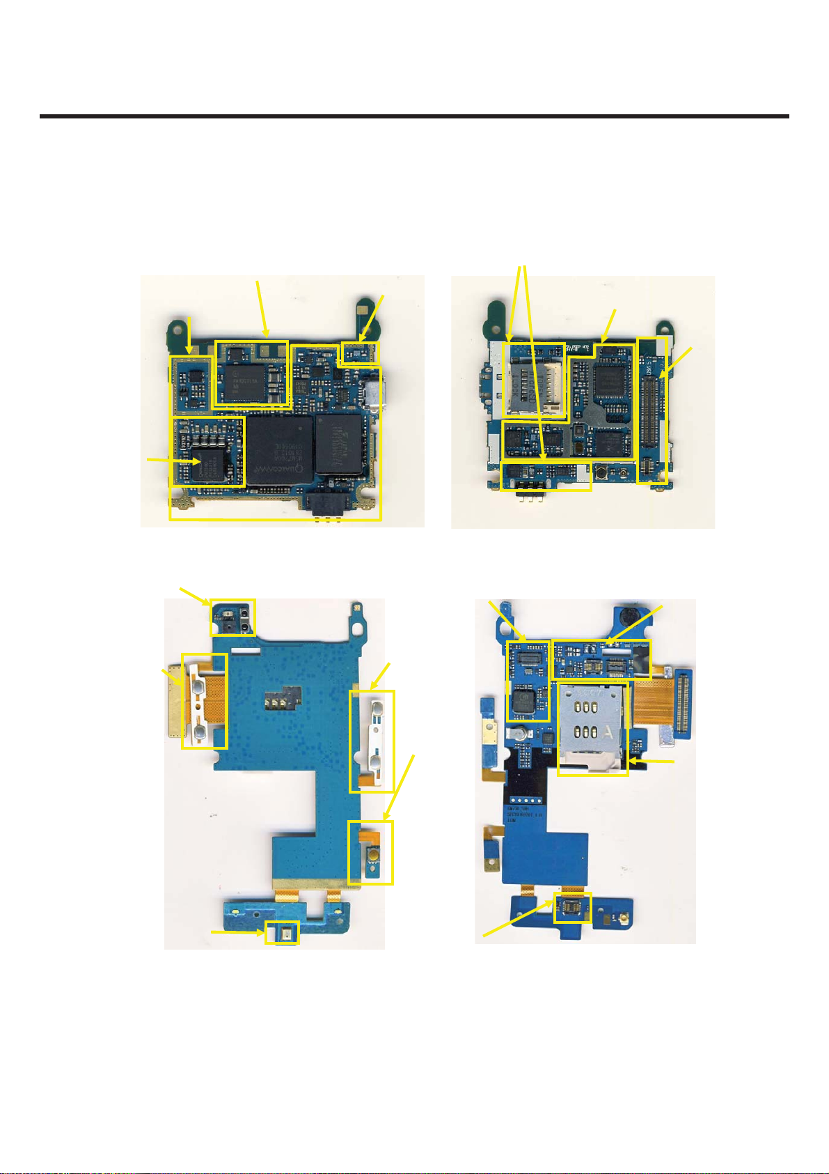
2. GM730 Main Component
WLAN,BT,FM
BB/MEM/Logic
PMIC
3. TECHNICAL BRIEF
Logic
RF
RF & GPS
Logic
VGA
Camera &
Sensor
Volume
SIDEKEY
Main board, Top
MIC
Power &
Reset
SIDEKEY
Camera
SIDEKEY
Main board, Bottom
5M Camera
Optical Joystick
Logic
USIM
Sub board, Top
Copyright © 2009 LG Electronics. Inc. All right reserved.
Only for training and service purposes
- 29 -
Sub board, Bottom
LGE Internal Use Only
3. TECHNICAL BRIEF
RF
S501
FL106
FL107
FL111
FL108
U107
U106
U105
U104
U108
FL110
U102
FL104
FL103
FL101
FL100
FL109
FL105
U101
FL112
SW100
U103
DescriptionReferenceDescriptionReference
FL107RTR6285(Transceiver)U102
FL105FEM & GSM PAMU101
FL112WCDMA Dual (I,VIII) PAMU104
FL109WCDMA (II) PAMU107
FL106WCDMA (II) TX SAW FilterFL111
U108WCDMA (I) TX SAW FilterFL108
FL110WCDMA (II) CouplerU106
FL100EGSM Rx SAW FilterFL101
FL104WCDMA (I) CouplerU105
FL103WCDMA (VIII) CouplerU103
WCDMA (VIII) TX SAW
WCDMA (VIII) Duplexer
WCDMA (II) Duplexer
WCDMA (I) Duplexer
WCDMA (I) RX SAW Filter
GPS LNA
GPS SAW Filter
GSM850 Rx SAW Filter
PCS Rx SAW Filter
DCS Rx SAW Filter
Micro-SD SocketS501Test ConnectorSW101
LGE Internal Use Only Copyright © 2009 LG Electronics. Inc. All right reserved.
- 30 -
Only for training and service purposes
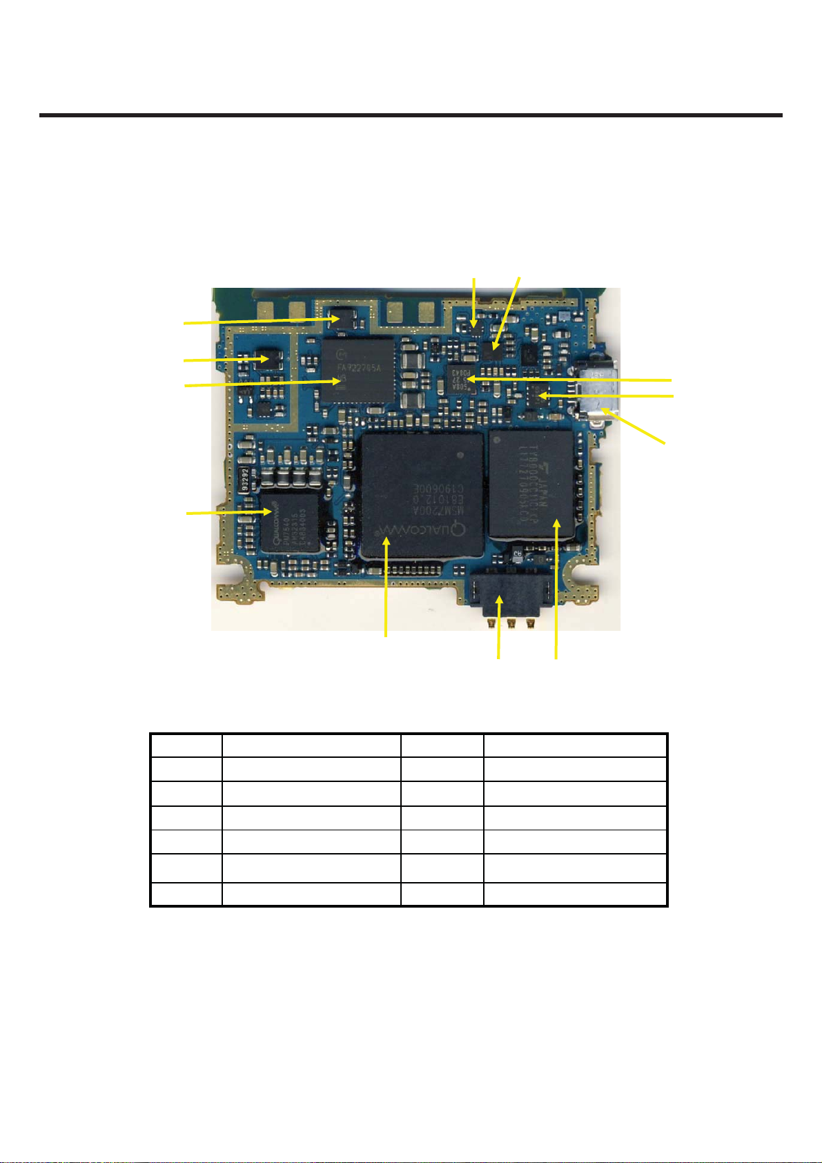
Logic / BB / MEM / Audio/WLAN
3. TECHNICAL BRIEF
X501
X201
U503
U405
U203
U501
U502
CN402
U402
U401
CN401
U302
Copyright © 2009 LG Electronics. Inc. All right reserved.
Only for training and service purposes
- 31 -
DescriptionRef.DescriptionRef.
Battery ConnectorCN402TCXO (9.2MHz)X201
Audio SubsystemU501TCXO (26MHz)X501
Audio SubsystemU502Wi-Fi &BT & FM ModuleU503
USB TransceiverU402PMIC, PM7540U405
Over-voltage ProtectionU401MCU, MSM7200AU203
Micro USB 5Pin Con.CN401Memory, MCPU302
LGE Internal Use Only
 Loading...