

LG GM72V66841CT-8, GM72V66841CT-7K, GM72V66841CT-7J, GM72V66841CT-10K, GM72V66841CLT-8 Datasheet
...
LG Semicon Co.,Ltd.
REVISION HISTORY
/ Revision 1.0: July 1998
- Add PC100,7K(2-2-2) Specifications.
- Update Icc Specifications.
- Change Input Test Condition from 2.8/0.0V to 2.4/0.4V.
- Added post SPD Information separately(7K/7J/10K) for Modules.
- Add Minimum Capacitance Value for Component.
Rev. 1.0
GM72V66841CT/CLT
2,097,152 WORD x 8 BIT x 4 BANK
SYNCHRONOUS DYNAMIC RAM
Description
The GM72V66841CT/CLT is a synchronous
dynamic random access memory comprised of
67,108,864 memory cells and logic including
input and output circuits operating synchronously
by referring to the positive edge of the externally
provided Clock.
The GM72V66841CT/CLT provides four
banks of 2,097,152 word by 8 bit to realize high
bandwidth with the Clock frequency up to 125
Mhz.
Features
* PC100,PC66 Compatible
7K(2-2-2), 7J(3-2-2), 10K(PC66)
* 3.3V single Power supply
* LVTTL interface
* Max Clock frequency
100/125 MHz
* 4,096 refresh cycle per 64 ms
* Two kinds of refresh operation
Auto refresh/ Self refresh
* Programmable burst access capability ;
- Sequence:Sequential / Interleave
- Length :1/2/4/8/FP
* Programmable CAS latency : 2/3
* 4 Banks can operate independently or
simultaneously
* Burst read/burst write or burst read/single
write operation capability
* Input and output masking by DQM input
* One Clock of back to back read or write
command interval
* Synchronous Power down and Clock
suspend capability with one Clock latency
for both entry and exit
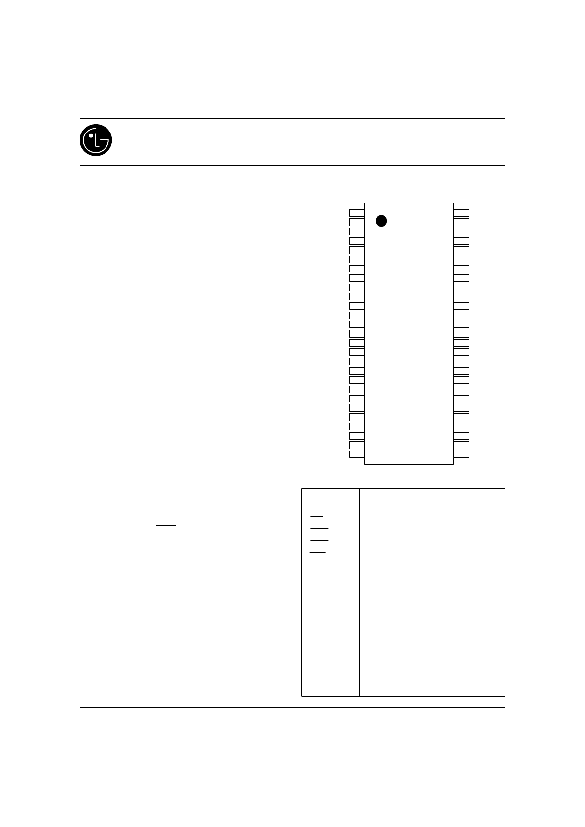
*JEDEC Standard 54Pin 400mil TSOP II
Package
Pin Configuration
LG Semicon Co.,Ltd.
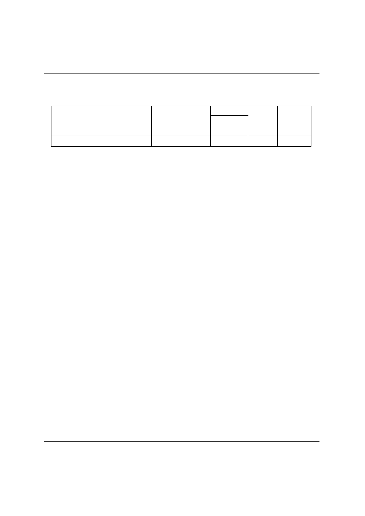
Pin Name
CLK
CKE
CS
RAS
CAS
WE
A0~A9,A11
A10 / AP
BA0/A13
~BA1/A12
DQ0~DQ7
DQM
VCCQ
VSSQ
VCC
VSS
NC
Clock
Clock Enable
Chip Select
Row Address Strobe
Column Address Strobe
Write Enable
Address input
Address input or Auto Precharge
Bank select
Data input / Data output
Data input / output Mask
VCC for DQ
VSS for DQ
Power for internal circuit
Ground for internal circuit
No Connection
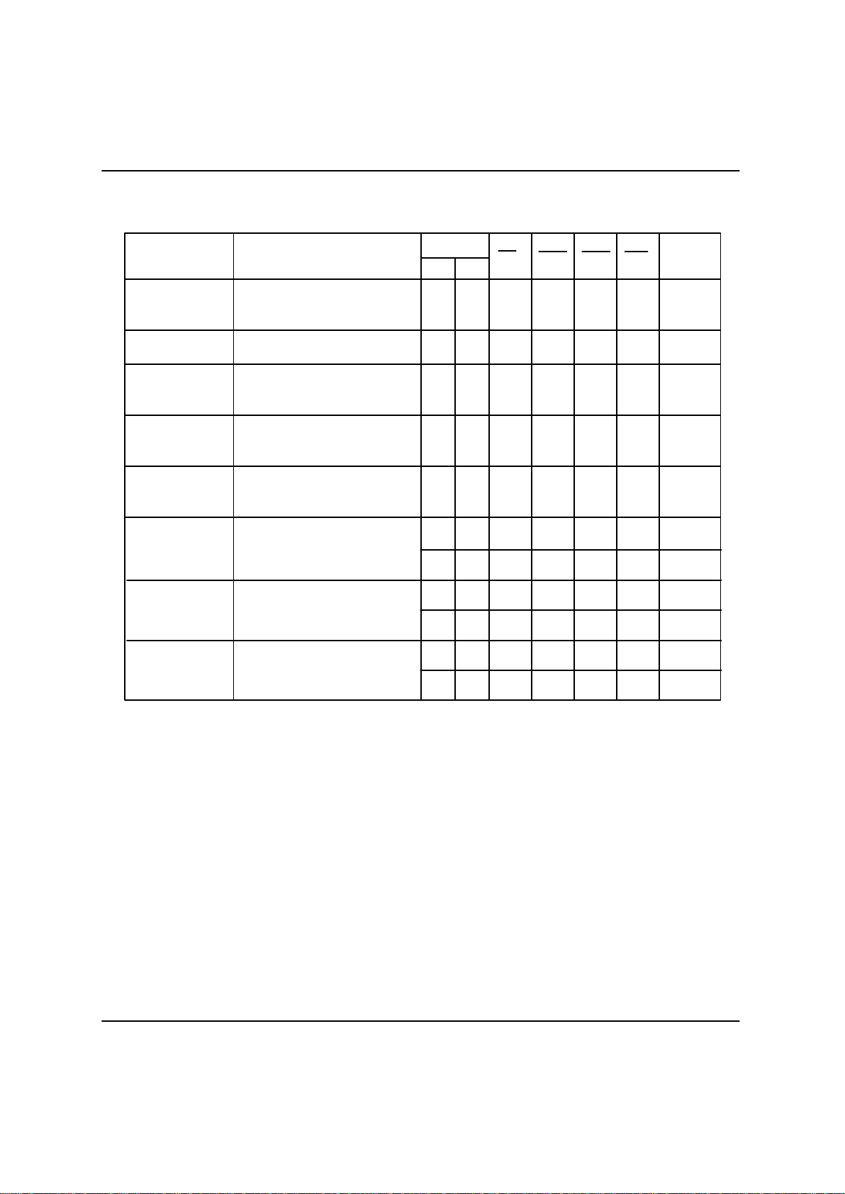
1
2
3
4
5
6
7
8
9
10
11
12
13
14
15
16
17
18
19
20
21
22
23
24
25
26
27
JEDEC STANDARD
400 mil 54 PIN TSOP II
(TOP VIEW)
54
53
52
51
50
49
48
47
46
45
44
43
42
41
40
39
38
37
36
35
34
33
32
31
30
29
28
VCC
DQ0
VCCQ
NC
DQ1
VSSQ
NC
DQ2
VCCQ
NC
DQ3
VSSQ
NC
VCC
NC
/WE
/CAS
/RAS
/CS
BA0/A13
BA1/A12
A10,AP
A0
A1
A2
A3
VCC
VSS
DQ7
VSSQ
NC
DQ6
VCCQ
NC
DQ5
VSSQ
NC
DQ4
VCCQ
NC
VSS
NC
DQM
CLK
CKE
NC
A11
A9
A8
A7
A6
A5
A4
VSS
1
LG Semicon
GM72V66841CT/CLT
2
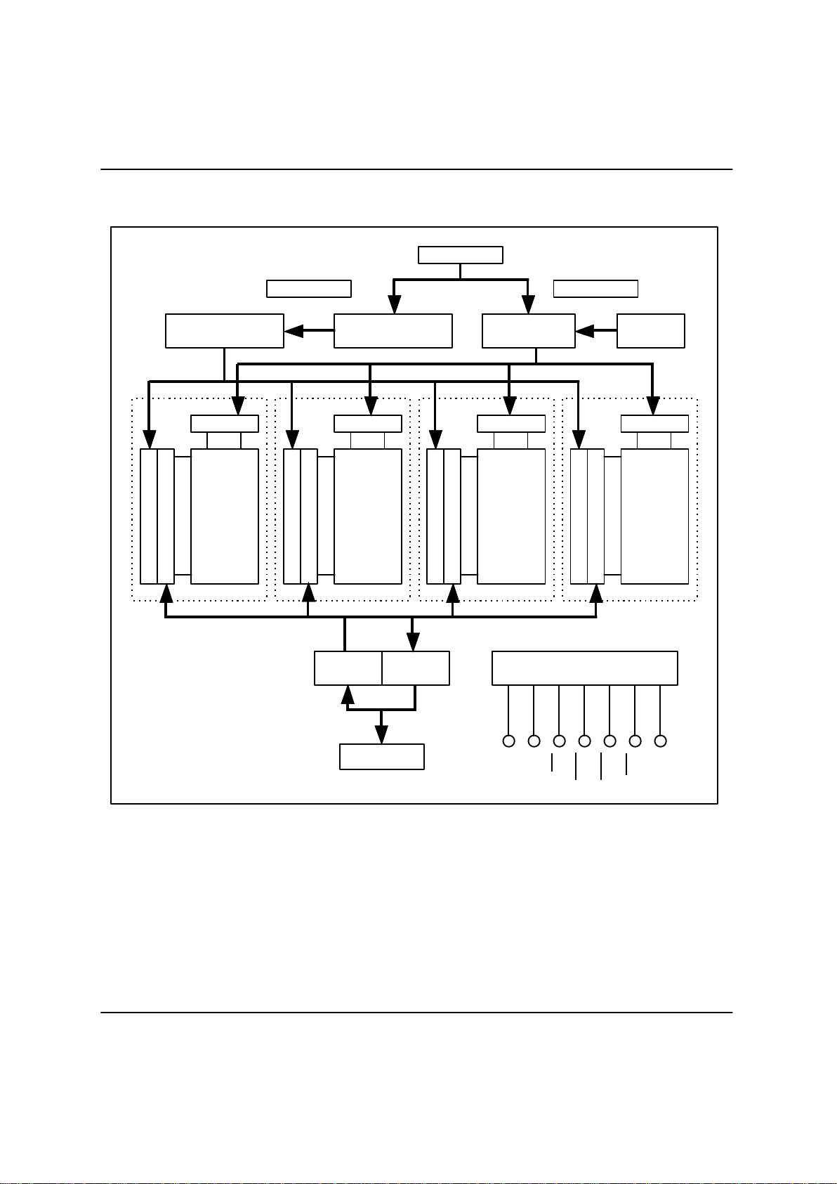
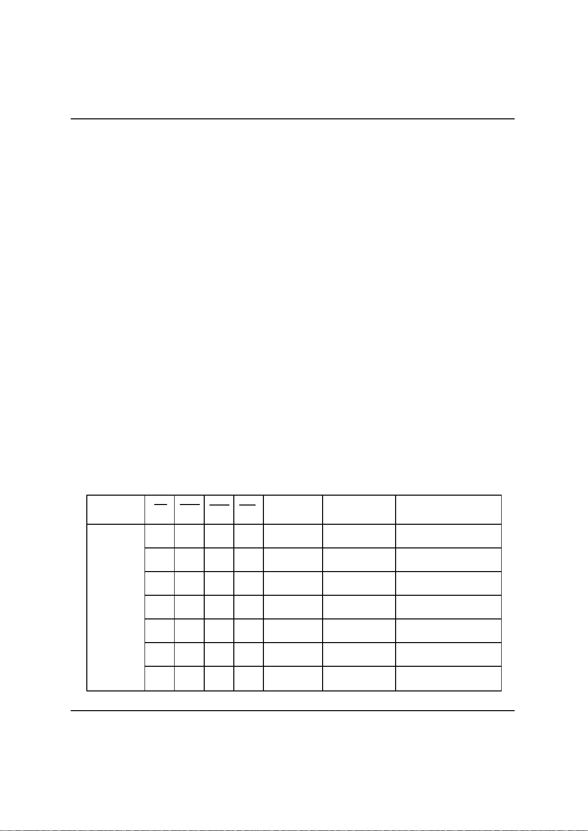
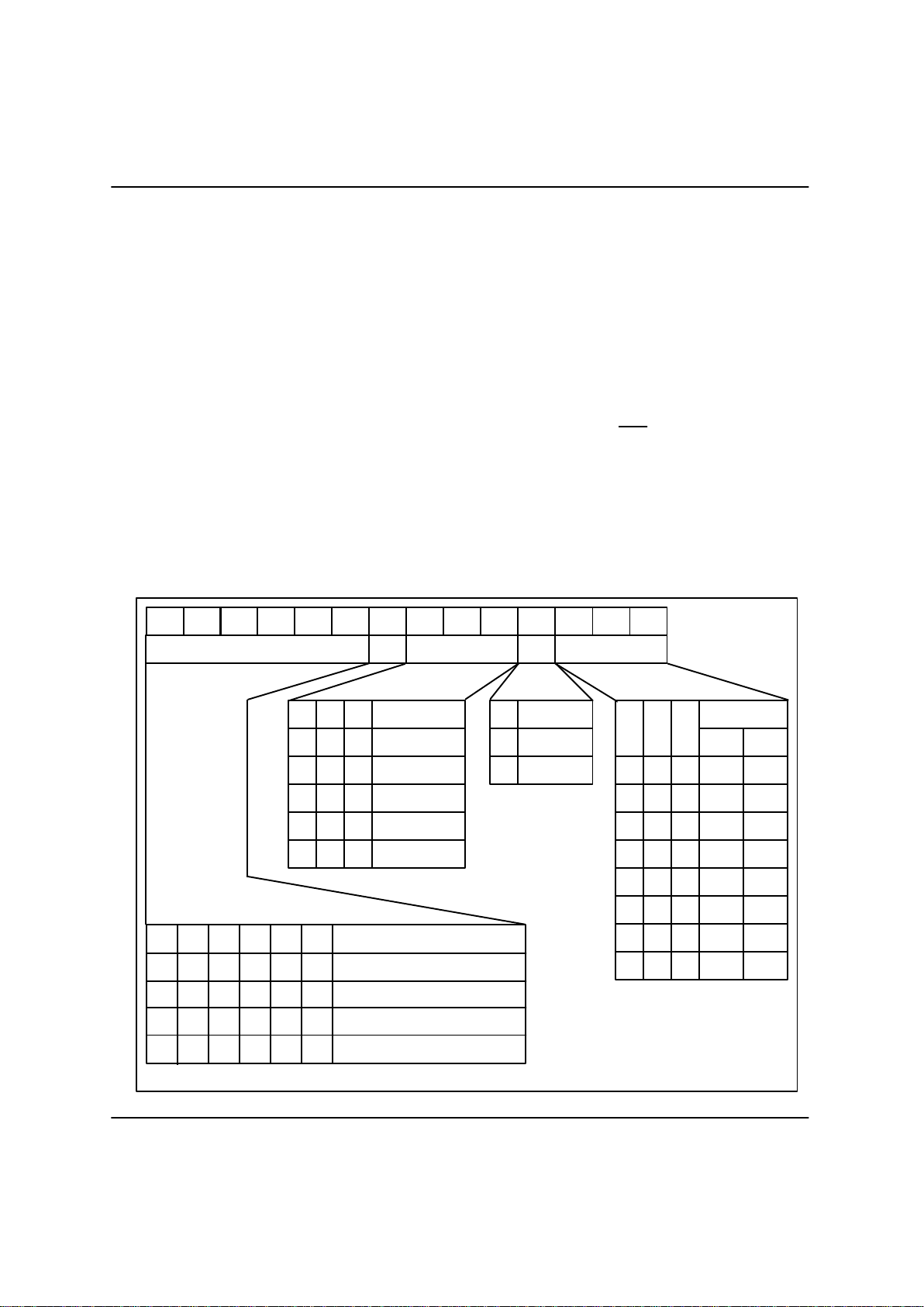
Block Diagram
A0 to A13
A0 to A8 A0 to A13
Column address
counter
Column address
buffer
Row address
counter
Refresh
counter
Input
buffer
Output
buffer
DQ0 to DQ7
Control logic &
timing generator
CLK
CKE
DQM
RAS
CAS
Row decoder
Memory array
Bank 0
4096 row
x 512 column
x 8 bit
Column decoder
Sense amplifier & I/O bus
Row decoder
Memory array
Bank 1
4096 row
x 512 column
x 8 bit
Column decoder
Sense amplifier & I/O bus
Row decoder
Memory array
Bank 2
4096 row
x 512 column
x 8 bit
Column decoder
Sense amplifier & I/O bus
Row decoder
Memory array
Bank 3
4096 row
x 512 column
x 8 bit
Column decoder
Sense amplifier & I/O bus
CS
WE
LG Semicon
GM72V66841CT/CLT
Pin Description
Pin Name DESCRIPTION
CLK
(input pin)
CLK is the master Clock input to this pin. The other input signals are referred
at CLK rising edge.
CKE
(input pin)
This pin determines whether or not the next CLK is valid. If CKE is High, the
next CLK rising edge is valid. If CKE is Low, the next CLK rising edge is
invalid. This pin is used for Power-down and Clock suspend modes.
CS
(input pin)
When CS is Low, the command input cycle becomes valid. When CS is high,
all inputs are ignored. However, internal operations (bank active, burst
operations, etc.) are held.
Although these pin names are the same as those of conventional DRAMs,
they function in a different way. These pins define operation commands (read,
write, etc.) depending on the combination of their voltage levels. For details,
refer to the command operation section.
RAS, CAS, and WE
(input pins)
A0 ~ A11
(input pins)
Row address (AX0 to AX11) is determined by A0 to A11 level at the bank
active command cycle CLK rising edge. Column address(AY0 to AY8;
GM72V66841CT/CLT) is determined by A0 to A8 level at the read or write
command cycle CLK rising edge. And this column address becomes burst
access start address. A10 defines the Precharge mode. When A10 = High at
the Precharge command cycle, all banks are Precharged. But when A10 =
Low at the Precharge command cycle, only the bank that is selected by
A12/A13 (BS) is Precharged.
A12/A13
(input pin)
A12/A13 are bank select signal (BS). The memory array of the
GM72V66841CT/CLT is divided into bank 0, bank 1, bank2 and bank 3.
GM72V66841CT/CLT contain 4096-row x 512-column x 8-bits. If A12 is
Low and if A13 is Low, bank 0 is selected. If A12 is High and A13 is Low,
bank 1 is selected. If A12 is Low and A13 is High, bank 2 is selected. If A12
is High and A13 is High, bank 3 is selected.
DQM,
DQMU/DQML
(input pins)
DQM, DQMU/DQML controls input/output buffers.
* Read operation: If DQM, DQMU/DQML is High, The output buffer
becomes High-Z. If the DQM, DQMU/DQML is Low, the output buffer
becomes Low-Z.
* Write operation: If DQM, DQMU/DQML is High, the previous data is held
(the new data is not written). If DQM, DQMU/DQML is Low, the data is
written.
3
LG Semicon
GM72V66841CT/CLT
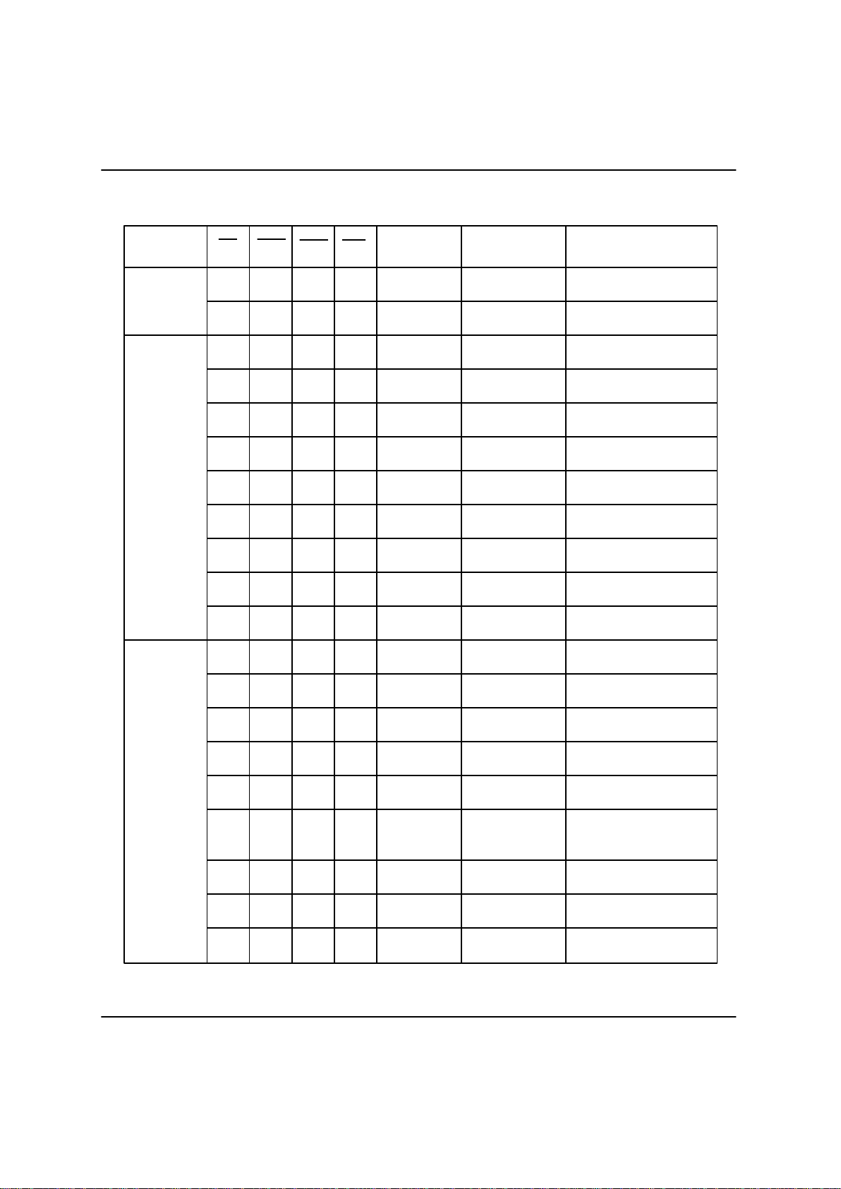
Command Operation
Command Truth Table
* Notes : H: VIH, L: VIL, X: VIH or VIL, V: Valid address input
The synchronous DRAM recognizes the following commands specified by the CS, RAS, CAS, WE
and address pins.
Function
Ignore command
Symbol
CKE
No Operation
Burst stop in full page
Column address and
read command
Read with auto-Precharge
Write with auto-Precharge
Row address strobe and
bank active
Precharge all banks
Column address and
write command
CS RAS CAS WE
A12~
A13
A10
A0~
A11
DESL
NOP
BST
READ
READ A
WRIT
WRIT A
ACTV
PALL
H
H
H
H
H
H
H
H
H
H
X
X
X
X
X
X
X
X
X
V
H
L
L
L
L
L
L
L
L
L
X
H
H
H
H
H
H
L
L
L
X
H
H
L
L
L
L
H
H
L
X
H
L
H
H
L
L
H
L
H
X
X
X
V
V
V
V
V
X
X
X
X
X
L
H
L
H
V
H
X
X
X
X
V
V
V
V
V
X
X
n-1
n
H X L L L L V V V
Mode register set
MRS
Refresh
REF/SELF
Precharge select bank
PRE H X L L H L V L X
4
VSS and VSSQ
(Power supply pins)
Ground is connected. (VSS is for the internal circuit and VSSQ is for the output
buffer.)
NC No Connection pins.
DESCRIPTION
Pin Name
VCC and VCCQ
(Power supply pins)
3.3 V is applied. (VCC is for the internal circuit and VCCQ is for the output
buffer.)
DQ0 ~ DQ7
(I/O pins)
Data is input and output from these pins. These pins are the same as those of a
conventional DRAM.
Pin Description(Continued)

LG Semicon
GM72V66841CT/CLT
Burst stop in full page [BST] : This
command stops a full-page burst operation (burst
length = full-page(512;GM72V66841CT/CLT)
and is illegal otherwise. Full page burst continues
until this command is input. When data
input/output is completed for full-page of data, it
automatically returns to the start address, and
input/output is performed repeatedly.
Column address strobe and read command
[READ]: This command starts a read operation.
In addition, the start address of burst read is
determined by the column address
AY0 to AY8; GM72V66841CT/CLT) and the
bank select address (A12/A13). After the read
operation, the output buffer becomes High-Z.
Read with auto-Precharge [READ A]: This
command automatically performs a Precharge
operation after a burst read with a burst length of
1, 2, 4 or 8. When the burst length is full-page,
this command is illegal.
Column address strobe and write command
[WRIT]: This command starts a write operation.
When the burst write mode is selected, the column
address (AY0 to AY8; GM72V66841CT/CLT)
and the bank select address (A12/A13) become the
burst write start address. When the single write
mode is selected, data is only written to the
location specified by the column address (AY0 to
AY8;GM72V66841CT/CLT) and the bank select
address (A12/A13).
Write with auto-Precharge [WRIT A]: This
command automatically performs a Precharge
operation after a burst write with a length of 1, 2,
4 or 8, or after a single write operation. When the
burst length is full-page, this command is illegal.
Row address strobe and bank activate
[ACTV]: This command activates the bank that
is selected by A12/A13(BS) and determines the
row address (AX0 to AX11). If A12 is Low and
if A13 is Low, bank 0 is activated. If A12 is High
and A13 is Low, bank 1 is activated. If A12 is
Low and A13 is High, bank 2 is activated. If A12
is High and A13 is High, bank 3 is activated.
Precharge selected bank [PRE]: This
command starts Precharge operation for the bank
selected by A12/A13. If A12 is Low and if A13 is
Low, bank 0 is selected. If A12 is High and A13
is Low, bank 1 is selected. If A12 is Low and
A13 is High, bank 2 is selected. If A12 is High
and A13 is High, bank 3 is selected.
Precharge all banks [PALL]: This command
starts a Precharge operation for all banks.
Refresh [REF/SELF]: This command starts the
refresh operation. There are two types of refresh
operation, the one is auto-refresh, and the other is
self-refresh. For details, refer to the CKE truth
table section.
Mode register set [MRS]: Synchronous DRAM
has a mode register that defines how it operates.
The mode register is specified by the address pins
(A0 to A11) at the mode register set cycle. For
details, refer to the mode register configuration.
After Power on, the contents of the mode register
are undefined, execute the mode register set
command to set up the mode register.
5
Ignore command [DESL]: When this command
is set (CS is High), the synchronous DRAM
ignores command input at the Clock. However,
the internal status is held.
No operation [NOP]: This command is not an
execution command. However, the internal
operations continue.
LG Semicon
GM72V66841CT/CLT
6
DQM Truth Table
Function
Write enable/output enable
Write inhibit/output disable
Symbol
ENB
MASK
n-1
CKE
DQM
n
H
H
X
X
L
H
The GM72V66841CT/CLT can mask input/output
data by means of DQM.
During reading, the output buffer is set to Low-Z
by setting DQM to Low, enabling data output. On
the other hand, when DQM is set to High, the
output buffer becomes High-Z, disabling data
output.
During writing, data is written by setting DQM to
Low. When DQM is set to High, the previous
data is held (the new data is not written). Desired
data can be masked during burst read or burst
write by setting DQM. For details, refer to the
DQM control section of the
GM72V66841CT/CLT operating instructions.
* Notes : H: VIH, L: VIL, X: VIH or VIL.
Write : lDID is needed.
Read : lDOD is needed.
LG Semicon
GM72V66841CT/CLT
7
WRITE suspend and WRIT A suspend: In
this mode, external signals are not accepted.
However, the internal state is held.
Clock suspend: During Clock suspend mode,
keep the CKE to Low.
Clock suspend mode exit : The synchronous
DRAM exits from Clock suspend mode by
setting CKE to High during the Clock suspend
state.
IDLE: In this state, all banks are not selected,
and completed Precharge operation.
Clock suspend mode entry: The synchronous
DRAM enters Clock suspend mode from active
mode by setting CKE to Low. The Clock suspend
mode changes depending on the current status (1
Clock before) as shown below.
ACTIVE Clock suspend: This suspend mode
ignores inputs after the next Clock by internally
maintaining the bank active status.
READ suspend and READ A suspend: The
data being output is held (and continues to be
output).
* Notes : H: VIH, L: VIL, X: VIH or VIL.
Power down
Idle
Power down
entry
Self refresh
exit
Power down
Exit
H
L
L
L
H
H
L
L
H H H X
Self refresh
(SELFX)
H L H X X X X
H H H X
H H H XL
L H H X X X X
L H X X X XH
Current
State
Active
CKE
Any
Clock Suspend
Idle
Idle
Clock suspend
mode entry
Clock suspend
Clock suspend
mode exit
Auto-refresh
command
Self-refresh
entry
H
L
L
H
H
L
L
H
H
L
H
X
X
L
L
X
X
X
L
L
X
X
X
L
L
X
X
X
H
H
X
X
X
X
X
Function
(REF)
(SELF)
n -1
n
CS RAS CAS WE
Address
CKE Truth Table
LG Semicon
GM72V66841CT/CLT
Self-refresh exit[SELFX]: When this command
is executed during self-refresh mode, the
synchronous DRAM can exit from self-refresh
mode. After exiting from self-refresh mode, the
synchronous DRAM enters the IDLE state.
Power down mode entry: When this command
is executed during the IDLE state, the
synchronous DRAM enters Power down mode.
In Power down mode, Power consumption is
suppressed by cutting off the initial input circuit.
Power down exit: When this command is
executed at the Power down mode, the
synchronous DRAM can exit from Power down
mode. After exiting from Power down mode, the
synchronous DRAM enters the IDLE state.
Auto-refresh command[REF]: When this
command is input from the IDLE state, the
synchronous DRAM starts auto-refresh
operation. (The auto-refresh is the same as the
CBR refresh of conventional DRAMs.) During
the auto-refresh operation, refresh address and
bank select address are generated inside the
synchronous DRAM. For every auto-refresh
cycle, the internal address counter is updated.
Accordingly, 4,096 times are required to refresh
the entire memory. Before executing the autorefresh command, all the banks must be in the
IDLE state. In addition, since the Precharge for
all banks is automatically performed after autorefresh, no Precharge command is required after
auto-refresh.
Self-refresh entry[SELF]: When this command
is input during the IDLE state, the synchronous
DRAM starts self-refresh operation. After the
execution of this command, self-refresh
continues while CKE is Low. Since self-refresh
is performed internally and automatically,
external refresh operations are unnecessary.
Function Truth Table
The following table shows the operations that are performed when each command is issued in each
mode of the synchronous DRAM.
Current
state
Precharge
CS RAS CAS WE Address
H X X X X
L H H H X
L H H L X
L H L H BA, CA, A10
L H L L BA, CA, A10
L L H H BA, RA
L L H L BA, A10
Command Operation
DESL
NOP
BST
READ/READ A
WRIT/WRIT A
ACTV
PRE, PALL
Enter IDLE after tRP
Enter IDLE after tRP
NOP
ILLEGAL
ILLEGAL
ILLEGAL
NOP
8
LG Semicon
GM72V66841CT/CLT
Function Truth Table (Continued)
Current
state
Precharge
CS RAS CAS WE Address
H X X X X
L H H H X
L H H L X
L H L H BA, CA, A10
L H L L BA, CA, A10
L L H H BA, RA
L L H L BA, A10
L L L H X
L L L L MODE
Command Operation
DESL
NOP
BST
READ/READ A
WRIT/WRIT A
ACTV
PRE, PALL
REF, SELF
MRS
NOP
NOP
NOP
ILLEGAL
ILLEGAL
Bank and row active
NOP
Refresh
Mode register set
L L L H X
L L L L MODE
REF, SELF
MRS
ILLEGAL
ILLEGAL
Idle
Row active H X X X X
L H H H X
L H H L X
L H L H BA, CA, A10
L L H H BA, RA
L L H L BA, A10
L L L H X
DESL
NOP
BST
READ/READ A
ACTV
PRE, PALL
REF, SELF
NOP
NOP
NOP
Begin read
Precharge
ILLEGAL
L L L L MODE MRS ILLEGAL
L H L L BA, CA, A10 WRIT/WRIT A Begin write
Other bank active
ILLEGAL on same bank
*3
9
LG Semicon
GM72V66841CT/CLT
Function Truth Table (Continued)
Current
state
Read
CS RAS CAS WE Address
L H H H X
L H H L X
L H L H BA, CA, A10
L H L L BA, CA, A10
L L H H BA, RA
L L H L BA, A10
L L L H X
L L L L MODE
Command Operation
NOP
BST
READ/READ A
WRIT/WRIT A
ACTV
PRE, PALL
REF, SELF
MRS
Continue burst to end
Burst stop to full page
Term burst read/start
write
Term burst read and
Precharge
ILLEGAL
ILLEGAL
H X X X X DESL Continue burst to end
Read with
autoPrecharge
H X X X X
L H H H X
L H H L X
L H L L BA, CA, A10
L L H H BA, RA
L L H L BA, A10
DESL
NOP
BST
WRIT/WRIT A
ACTV
PRE, PALL
Continue burst to end
and Precharge
Continue burst to end
and Precharge
ILLEGAL
ILLEGAL
L L L H X REF, SELF ILLEGAL
L H L H BA, CA, A10 READ/READ A ILLEGAL
ILLEGAL
Other bank active
ILLEGAL on same bank
*3
Continue burst read to
CAS latency and New
read
L L L L MODE MRS ILLEGAL
Other bank active
ILLEGAL on same bank
*3
10
LG Semicon
GM72V66841CT/CLT
Function Truth Table (Continued)
Current
state
Write
CS RAS CAS WE Address
L H H H X
L H H L X
L H L H BA, CA, A10
L H L L BA, CA, A10
L L H H BA, RA
L L H L BA, A10
L L L H X
L L L L MODE
Command Operation
NOP
BST
READ/READ A
WRIT/WRIT A
ACTV
PRE, PALL
REF, SELF
MRS
Continue burst to end
Burst stop on full page
Term burst and New
write
ILLEGAL
ILLEGAL
H X X X X DESL Continue burst to end
Write with
autoPrecharge
H X X X X
L H H H X
L H H L X
L H L L BA, CA, A10
L L H H BA, RA
L L H L BA, A10
DESL
NOP
BST
WRIT/WRIT A
ACTV
PRE, PALL
Continue burst to end
and Precharge
Continue burst to end
and Precharge
ILLEGAL
ILLEGAL
L L L H X REF, SELF ILLEGAL
L H L H BA, CA, A10 READ/READ A ILLEGAL
ILLEGAL
Other bank active
ILLEGAL on same bank
*3
Term burst and New
read
L L L L MODE MRS ILLEGAL
Term burst write and
Precharge
*2
Other bank active
ILLEGAL on same bank
*3
11
LG Semicon
GM72V66841CT/CLT
From [Precharge]
To [DESL], [NOP] or [BST]: When these
commands are executed, the synchronous
DRAM enters the IDLE state after tRP has
elapsed from the completion of Precharge
From [IDLE]
To [DESL], [NOP], [BST], [PRE] or
[PALL]: These commands result in no
operation.
To [ACTV]: The bank specified by the
address pins and the ROW address is
activated.
To [REF], [SELF]: The synchronous
DRAM enters refresh mode (auto-refresh or
self-refresh).
To [MRS]: The synchronous DRAM enters
the mode register set cycle.
From [ROW ACTIVE]
To [DESL], [NOP] or [BST]: These
commands result in no operation.
To [READ], [READ A]: A read operation
starts. (However, an interval of tRCD is
required.)
To [WRIT], [WRIT A]: A write operation
starts. (However, an interval of tRCD is
required.)
To [ACTV]: This command makes the
other bank active. (However, an interval of
tRRD is required.) Attempting to make the
currently active bank active results in an
illegal command.
To [PRE], [PALL]: These commands set
the synchronous DRAM to Precharge
mode. (However, an interval of tRAS is
required.)
12
Function Truth Table (Continued)
Current
state
Refresh
(auto-refresh)
CS RAS CAS WE Address
L H H H X
L H H L X
L H L H BA, CA, A10
L H L L BA, CA, A10
L L H H BA, RA
L L H L BA, A10
L L L H X
L L L L MODE
Command Operation
NOP
BST
READ/READ A
WRIT/WRIT A
ACTV
PRE, PALL
REF, SELF
MRS
Enter IDLE after tRC
Enter IDLE after tRC
ILLEGAL
ILLEGAL
ILLEGAL
H X X X X DESL Enter IDLE after tRC
ILLEGAL
ILLEGAL
ILLEGAL
* Notes : 1. H: VIH, L: VIL, X: VIH or VIL.
The other combinations are inhibit.
2. An interval of tRWL is required between the final valid data input and the Precharge command.
3. If tRRD is not satisfied, this operation is illegal.
4. BA:Bank Address, RA:Row Address, CA:Column Address

LG Semicon
GM72V66841CT/CLT
From [WRITE with AUTO-Precharge]
To [DESL], [NOP]: These commands
continue write operations until the burst
operation is completed, and the synchronous
DRAM then enters Precharge mode.
To [ACTV]: This command makes the other
bank active. (However, an interval of tRC is
required.) Attempting to make the currently
active bank active results in an illegal
command.
To [DESL], [NOP], [BST]: After an autorefresh cycle (after tRC), the synchronous
DRAM automatically enters the Idle state.
From [REFRESH]
13
From [WRITE]
To [DESL], [NOP]: These commands
continue write operations until the burst
operation is completed.
To [BST]: This command stops a full-page
burst.
To [READ], [READ A]: These commands
stop a burst and start a read cycle.
To [WRIT], [WRIT A]: These commands
stop a burst and start the next write cycle.
To [ACTV]: This command makes the
other bank active. (However, an interval of
tRRD is required.) Attempting to make the
currently active bank active results in an
illegal command.
To [PRE], [PALL]: These commands stop
burst write and the synchronous DRAM
then enters Precharge mode.
From [READ]
From [READ with AUTO-Precharge]
To [DESL], [NOP]: These commands
continue read operations until the burst
operation is completed, and the synchronous
DRAM then enters Precharge mode.
To [ACTV]: This command makes other
banks bank-active. (However, an interval of
tRRD is required.) Attempting to make the
currently active bank active results in an
illegal command.
To [DESL], [NOP]: These commands
continue read operations until the burst
operation is completed.
To [BST]: This command stops a full-page
burst.
To [READ], [READ A]: Data output by the
previous read command continues to be
output. After CAS latency, the data output
resulting from the next command will start.
To [WRIT], [WRIT A]: These commands
stop a burst read, and start a write cycle.
To [ACTV]: This command makes other
banks bank-active. (However, an interval of
tRRD is required.) Attempting to make the
currently active bank active results in an
illegal command.
To [PRE], [PALL]: These commands stop a
burst read, and the synchronous DRAM
enters Precharge mode.
LG Semicon
GM72V66841CT/CLT
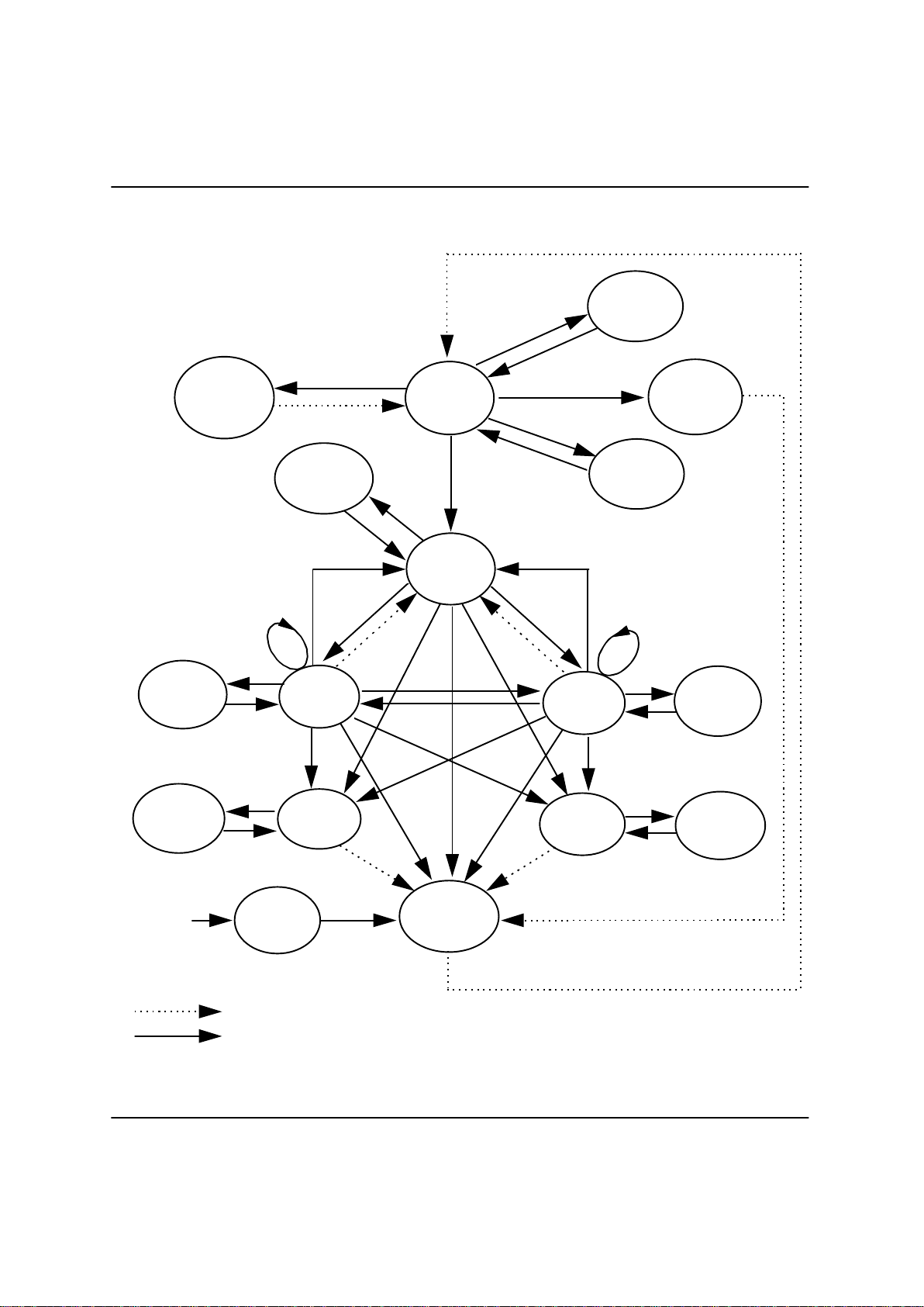
64M SDRAM Function State Diagram
Automatic Transition after completion of command.
Transition resulting from command input.
Power
ON
PRECHARGE
Precharge
IDLE
SR ENTRY
SR EXIT
SELF-
REFRESH
MODE
REGISTER
SET
MRS
REFRESH
AUTOREFRESH
IDLE
Power
DOWN
ROW
ACTIVE
ACTIVE
CKE=L
CKE=H
CKE=H
CKE=L
READ
READ
SUSPEND
WRITE
SUSPEND
READA
WRITEA
READA
SUSPEND
WRITEA
SUSPEND
CKE=L
CKE=H
CKE=L
CKE=H
WRITE
READ
WRITE WITH AP
PRECHARGE
READ WITH AP
WRITE
PRECHARGE
PRECHARGE
Read
Write
CKE=L
CKE=H
CKE=L
CKE=H
WRITE
READ
READ
WITH AP
READ
WITH AP
WRITE
WITH AP
WRITE
WITH AP
ACTIVE
Clock
SUSPEND
Power
APPLIED
BST
(on full page)
BST
(on full page)
14
Note: 1. After the auto-refresh operation, Precharge is performed automatically and enter the IDLE state.
*1
LG Semicon
GM72V66841CT/CLT
Mode Register Configuration
Burst read and SINGLE WRITE:
Data is only written to the column address
specified during the write cycle, regardless of the
burst length.
A7:
Keep this bit Low at the mode register set cycle.
A6, A5, A4: (LMODE):
These pins specify the CAS latency.
A3: (BT):
A burst type is specified . When full-page burst is
performed, only "sequential" can be selected.
A2, A1, A0: (BL):
These pins specify the burst length.
The mode register is set by the input to the
address pins (A0 to A13) during mode register
set cycles. The mode register consists of five
sections, each of which is assigned to address
pins.
A13, A12, A11, A10, A9, A8: (OPCODE):
The synchronous DRAM has two types of write
modes. One is the burst write mode, and the
other is the single write mode. These bits specify
write mode.
Burst read and BURST WRITE:
Burst write is performed for the specified burst
length starting from the column address specified
in the write cycle.
A11 A10 A9 A8 A7 A6 A5 A4 A3 A2 A1 A0
OPCODE 0 LMODE BT BL
A3
0
1
Burst Type
Sequential
Interleave
A6 A5 A4
0 0 0
0 0 1
0 1 0
0 1 1
CAS Latency
R
R
2
3
1 X X R
A2 A1 A0
0 0 0
0 0 1
0 1 0
0 1 1
1 0 0
1 0 1
1 1 0
1 1 1
Burst Length
BT=0
1
2
4
8
R
R
R
F.P.
BT=1
1
2
4
8
R
R
R
R
F.P. = Full Page
(512:GM72V66841CT/CLT)
R is Reserved (inhibit)
X: 0 or 1
15
A13 A12
Write mode
Burst read and BURST WRITE
R
Burst read and SINGLE WRITE
R
A13
0
A11 A10 A9 A8A12
X
X
X
0
X
X
X
0
X
X
X
0
0
1
1
0
1
0
1
0
X
X
X
LG Semicon
GM72V66841CT/CLT
Burst
Length
2
4
8
Starting Column
Address
A2 A1 A0 Sequential Interleave
V V 0
V V 1
V 0 0
V 0 1
V 1 0
0 0 0
0 1 0
1 0 0
1 1 0
V 1 1
0 0 1
0 1 1
1 0 1
1 1 1
0 - 1
1 - 0
0 - 1 - 2 - 3
1 - 2 - 3 - 0
2 - 3 - 0 - 1
3 - 0 - 1 - 2
0 - 1 - 2 - 3 - 4 - 5 - 6 - 7
1 - 2 - 3 - 4 - 5 - 6 - 7 - 0
2 - 3 - 4 - 5 - 6 - 7 - 0 - 1
3 - 4 - 5 - 6 - 7 - 0 - 1 - 2
4 - 5 - 6 - 7 - 0 - 1 - 2 - 3
5 - 6 - 7 - 0 - 1 - 2 - 3 - 4
6 - 7 - 0 - 1 - 2 - 3 - 4 - 5
7 - 0 - 1 - 2 - 3 - 4 - 5 - 6
0 - 1
1 - 0
0 - 1 - 2 - 3
1 - 0 - 3 - 2
2 - 3 - 0 - 1
3 - 2 - 1 - 0
0 - 1 - 2 - 3 - 4 - 5 - 6 - 7
1 - 0 - 3 - 2 - 5 - 4 - 7 - 6
2 - 3 - 0 - 1 - 6 - 7 - 4 - 5
3 - 2 - 1 - 0 - 7 - 6 - 5 - 4
4 - 5 - 6 - 7 - 0 - 1 - 2 - 3
5 - 4 - 7 - 6 - 1 - 0 - 3 - 2
6 - 7 - 4 - 5 - 2 - 3 - 0 - 1
7 - 6 - 5 - 4 - 3 - 2 - 1 - 0
Burst Sequence
16
Addressing(decimal)
* Notes : V : Valid Address
LG Semicon
GM72V66841CT/CLT
Operation of
GM72V661641CT/CLT, GM72V66841CT/CLT,
GM72V66441CT/CLT Series
Bank active: Before executing a read or write
operation, the corresponding bank and the row
address must be activated by the bank active
(ACTV) command. Bank 0, bank 1, bank 2 or
bank 3 is activated according to the status of the
A12/A13 pin, and the row address (AX0 to
AX11) is activated by the A0 to A11 pins at the
bank active command cycle. An interval of tRCD
is required between the bank active command
input and the following read/write command
input.
Read operation: A read operation starts when a
read command is input. Output buffer becomes
Low-Z in the (CAS Latency - 1) cycle after read
command set. GM72V66841CT/CLT can perform a
burst read operation.
Read / Write Operation
The burst length can be set to 1, 2, 4, 8 or full
page(512;GM72V66841CT/CLT). The start address
for a burst read is specified by the column
address (AY0 to AY8; GM72V66841CT/CLT) and
the bank select address (A12/A13) at the read
command set cycle. In a read operation, data
output starts after the number of cycles specified
by the CAS Latency. The CAS Latency can be
set to 2 or 3.
When the burst length is 1, 2, 4, or 8, the Dout
buffer automatically becomes High-Z at the next
cycle after the successive burst-length data has
been output.
When the burst length is full-page
(512;GM72V66841CT/CLT) data is repeatedly
output until the burst stop command is input.
The CAS latency and burst length must be
specified at the mode register.
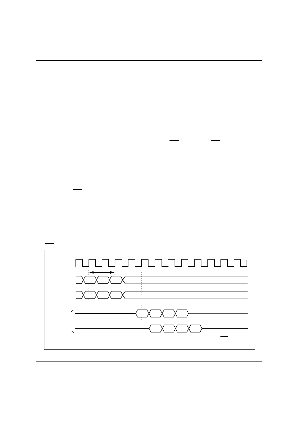
CAS Latency
CLK
Command
Address
Dout
CL : CAS Latency
Burst Length = 4
ACTV READ
Row
Column
CL = 2
CL = 3
out 2 out 3
out 1 out 2 out 3
tRCD
out 0 out 1
out 0
17
 Loading...