

LG GM310 Service Manual

Service Manual Model : GM310
Internal Use Only
Service Manual
GM310
Date: April, 2009 / Issue 1.0

Table Of Contents
1. INTRODUCTION ...............................................5
1.1 Purpose ......................................................................5
1.2 Regulatory Information .................................................5
1.3. ABBREVIATION ...........................................................7
2. PERFORMANCE ...............................................9
2.1 Supporting Standard ....................................................9
2.2 Main Parts : Solution ..................................................10
2.3 H/W features .............................................................10
2.4 HW Spec. ................................................................12
3. BB CIRCUIT TECHNICAL BRIEF .....................15
3.1 Functional Block Diagram ..........................................15
3.2 Baseband Processor Introduction ..............................15
3.3 Power management IC...............................................27
3.4 Power ON/OFF ..........................................................34
3.5 SIM Interface .............................................................35
3.6 MICRO SD connector .................................................36
3.7 Memory ....................................................................37
3.8 LCD Display ..............................................................38
3.9 Keypad switching & scanning .....................................39
3.10 keypad back-light illumination ..................................40
3.12 Battery voltage monitor ............................................42
3.13 Audio ......................................................................43
3.14 BLUETOOTH ............................................................46
3.15 18PIN Interface connector ........................................49
5.5 SIM Detect Trouble ....................................................73
5.6 Number Key Sense Trouble ........................................75
5.7 Multi Key sense Trouble .............................................77
5.8 Keypad backlight Trouble ...........................................79
5.9 Micro SD Trouble .......................................................81
5.10 Audio Trouble ..........................................................83
5.11 Microphone Trouble .................................................87
5.12 Camera Trouble .......................................................91
5.13 Main LCD Trouble ....................................................93
5.14 Bluetooth Trouble .....................................................95
5.15 RF Component ........................................................98
5.16 RF SIGNAL PATH .....................................................99
5.17 Trouble Shoothing of GSM Part ...............................100
5.18 Trouble Shooting of WCDMA Part ............................108
6. DOWNLOAD & S/W UPGRADE ..................... 115
7. BLOCK DIAGRAM ........................................ 126
8. CIRCUIT DIAGRAM ...................................... 127
9. BGA Pin Map .............................................. 137
10. PCB LAYOUT .............................................143
11. RF Calibration .......................................... 155
11.1. Test Equipment Setup ...........................................155
11.2. Calibration Step ....................................................155
4. RF Circuit Technical Brief ............................50
4.1 General Description ...................................................50
4.2 GSM Part ..................................................................53
4.3 WCDMA Part .............................................................57
4.4 GSM Power Amplifi er Module .....................................59
4.5 WCDMA Band1+8 Power Amplifi er Module .................60
4.6 WCDMA Band1+8 Low Noise Amplifi er .......................61
4.7 WCDMA Band1 Duplexer ...........................................62
4.8 WCDMA Band5 Duplexer ...........................................63
5. Trouble shooting .......................................... 64
5.1 Trouble shooting test setup ........................................64
5.2 Power on trouble .......................................................65
5.3 Charging Trouble .......................................................68
5.4 USB Trouble ..............................................................71
Copyright © 2009 LG Electronics. Inc. All right reserved.
Only for training and service purposes
12. EXPLODED VIEW & REPLACEMENT
PART LIST ................................................ 161
12.1 EXPLODED VIEW ...................................................161
12.2 Replacement Parts ................................................163
12.3 Accessory ............................................................. 191
- 3 -
LGE Internal Use Only

LGE Internal Use Only Copyright © 2009 LG Electronics. Inc. All right reserved.
- 4 -
Only for training and service purposes

1. INTRODUCTION
1. INTRODUCTION
1.1.Purpose
1. INTRODUCTION
This manual provides the information necessary to repair, calibration, description and download the
features of the
GM310.
1.2.Regulatory Information
A. Security
Toll fraud, the unauthorized use of telecommunications system by an unauthorized part (for example,
persons other than your company’s employees, agents, subcontractors, or person working on your
company’s behalf) can result in substantial additional charges for your telecommunications services.
System users are responsible for the security of own system.
There are may be risks of toll fraud associated with your telecommunications system. System users
are responsible for programming and configuring the equipment to prevent unauthorized use. LGE
does not warrant that this product is immune from the above case but will prevent unauthorized use of
common carrier telecommunication service of facilities accessed through or connected to it. LGE will
not be responsible for any charges that result from such unauthorized use.
B. Incidence of Harm
If a telephone company determines that the equipment provided to customer is faulty and possibly
causing harm or interruption in service to the telephone network, it should disconnect telephone
service until repair can be done. A telephone company may temporarily disconnect service as long as
repair is not done.
C. Changes in Service
A local telephone company may make changes in its communications facilities or procedure. If these
changes could reasonably be expected to affect the use of the
work, the telephone company is required to give advanced written notice to the user, allowing the user
to take appropriate steps to maintain telephone service.
GM310 or compatibility with the net
Copyright © 2009 LG Electronics. Inc. All right reserved.
Only for training and service purposes
- 5 -
LGE Internal Use Only

1. INTRODUCTION
GM310f service manual
D. Maintenance Limitations
Maintenance limitations on the GM310 must be performed only by the LGE or its authorized agent. The
user may not make any changes and/or repairs expect as specifically noted in this manual. Therefore,
note that unauthorized alternations or repair may affect the regulatory status of the system and may
void any remaining warranty.
E. Notice of Radiated Emissions
This model complies with rules regarding radiation and radio frequency emission as defined by local
regulatory agencies. In accordance with these agencies, you may be required to provide information
such as the following to the end user.
F. Pictures
The pictures in this manual are for illustrative purposes only; your actual hardware may look slightly
different.
G. Interference and Attenuation
An GM310 may interfere with sensitive laboratory equipment, medical equipment, etc. Interference
from unsuppressed engines or electric motors may cause problems.
H. Electrostatic Sensitive Devices
ATTENTION
Boards, which contain Electrostatic Sensitive Device (ESD), are indicated by the sign. Following
information is ESD handling:
• Service personnel should ground themselves by using a wrist strap when exchange system boards.
• When repairs are made to a system board, they should spread the floor with anti-static mat which is
also grounded.
• Use a suitable, grounded soldering iron.
• Keep sensitive parts in these protective packages until these are used.
• When returning system boards or parts like EEPROM to the factory, use the protective package as
described.
LGE Internal Use Only Copyright © 2009 LG Electronics. Inc. All right reserved.
- 6 -
Only for training and service purposes

1. INTRODUCTION
GM310f service manual
◆
◆
◆
◆
◆
◆
◆
◆
◆
◆
◆
◆
◆
◆
◆
◆
◆
◆
◆
◆
◆
◆
◆
◆
◆
◆
◆
1.3. ABBREVIATION
1. INTRODUCTION
For the purposes of this manual, following abbreviations apply:
APC Automatic Power Control
BB Baseband
BER Bit Error Ratio
CC-CV Constant Current – Constant Voltage
CLA Cigar Lighter Adapter
DAC Digital to Analog Converter
DCS Digital Communication System
dBm dB relative to 1 milli-watt
DSP Digital Signal Processing
EEPROM Electrical Erasable Programmable Read-Only Memory
EGPRS Enhanced General Packet Radio Service
EL Electroluminescence
ESD Electrostatic Discharge
FPCB Flexible Printed Circuit Board
GMSK Gaussian Minimum Shift Keying
GPIB General Purpose Interface Bus
GPRS General Packet Radio Service
GSM Global System for Mobile Communications
IPUI International Portable User Identity
IF Intermediate Frequency
LCD Liquid Crystal Display
LDO Low Drop Output
LED Light Emitting Diode
LGE LG Electronics
OPLL Offset Phase Locked Loop
PAM Power Amplifier Module
PCB Printed Circuit Board
Copyright © 2009 LG Electronics. Inc. All right reserved.
Only for training and service purposes
- 7 -
LGE Internal Use Only

1. INTRODUCTION
GM310f service manual
◆
◆
◆
◆
◆
◆
◆
◆
◆
◆
◆
◆
◆
◆
◆
◆
◆
◆
◆
PGA Programmable Gain Amplifier
PLL Phase Locked Loop
PSTN Public Switched Telephone Network
RF Radio Frequency
RLR Receiving Loudness Rating
RMS Root Mean Square
RTC Real Time Clock
SAW Surface Acoustic Wave
SIM Subscriber Identity Module
SLR Sending Loudness Rating
SRAM Static Random Access Memory
STMR Side Tone Masking Rating
TA Travel Adapter
TDD Time Division Duplex
TDMA Time Division Multiple Access
UART Universal Asynchronous Receiver/Transmitter
VCO Voltage Controlled Oscillator
VCTCXO
WAP Wireless Application Protocol
◆ 8PSK 8 Phase Shift Keying
Voltage Control Temperature Compensated Crystal
Oscillator
LGE Internal Use Only Copyright © 2009 LG Electronics. Inc. All right reserved.
- 8 -
Only for training and service purposes
2. PERFORMANCE
GM310f service manual
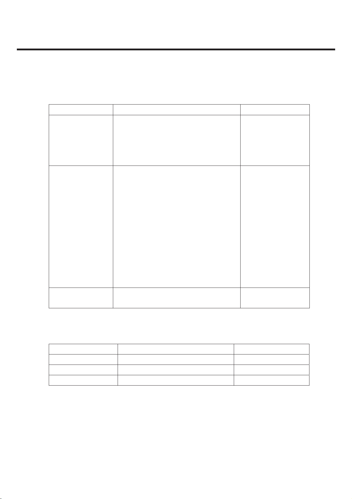
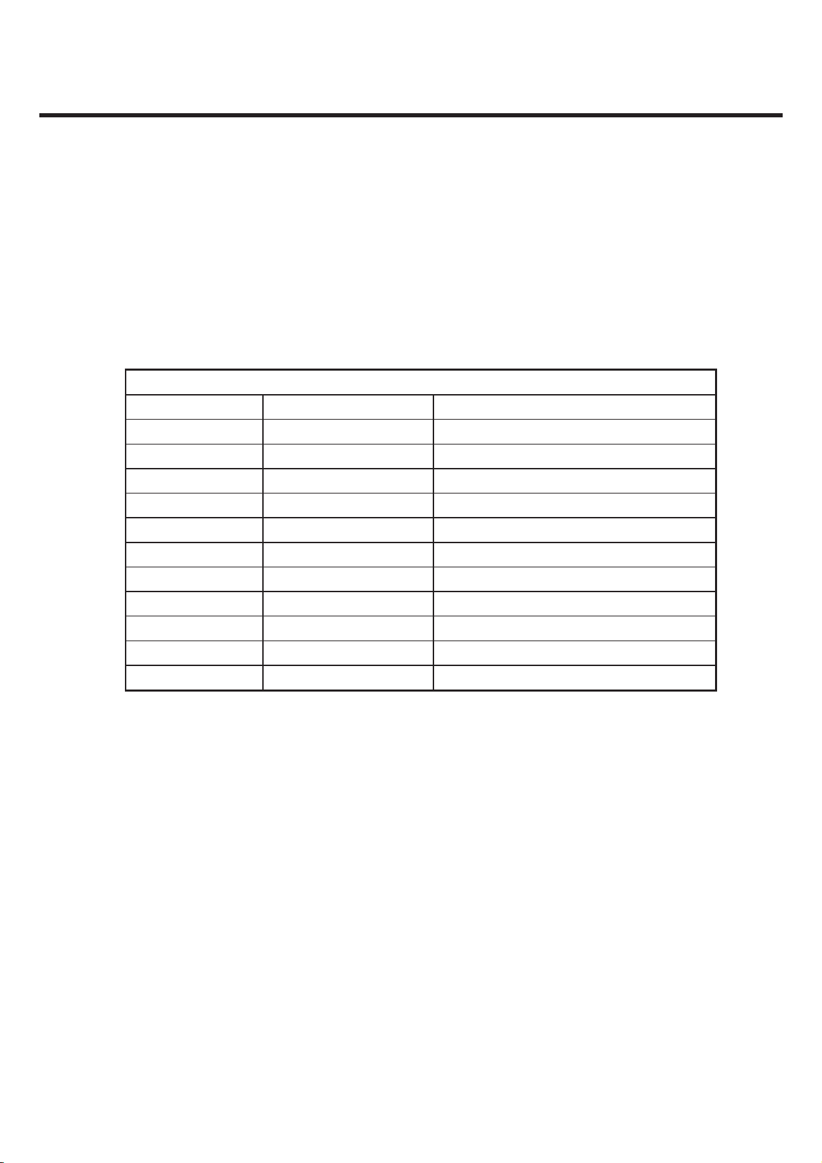
2.1 Supporting Standard
2. PERFORMANCE
Item Feature Comment
Supporting
Standard
Frequency Range GSM850 TX : 824 - 849 MHz
WCDMA 2100/850
GSM850/EGSM900/DCS1800/PCS1900
with seamless handover
Phase 2+(include AMR)
SIM Toolkit : Class 1, 2, 3, A-E
GSM850 RX :869 - 894 MHz
EGSM900 TX : 880 - 915 MHz
EGSM900 RX : 925 - 960 MHz
DCS1800 TX : 1710 - 1785 MHz
DCS1800 RX : 1805 - 1880 MHz
PCS1900 TX : 1850 - 1910 MHz
PCS1900 RX : 1930 - 1990 MHz
WCDMA2100 TX : 1920 - 1980 MHz
WCDMA2100 RX : 2110 - 2170 MHz
WCDMA850 TX : 824 - 849 MHz
WCDMA850 RX : 869 - 894 MHz
Application
Standard
WAP 2.0, JAVA 2.0
2.2 Main Parts : Solution
Item Part name Comment
Digital Baseband PMB8868 (Infineon)
Analog Baseband PMB8868 (Infineon)
RF chip PMB6952 (Infineon)
Copyright © 2009 LG Electronics. Inc. All right reserved.
Only for training and service purposes
- 9 -
LGE Internal Use Only
2. PERFORMANCE
GM310f service manual
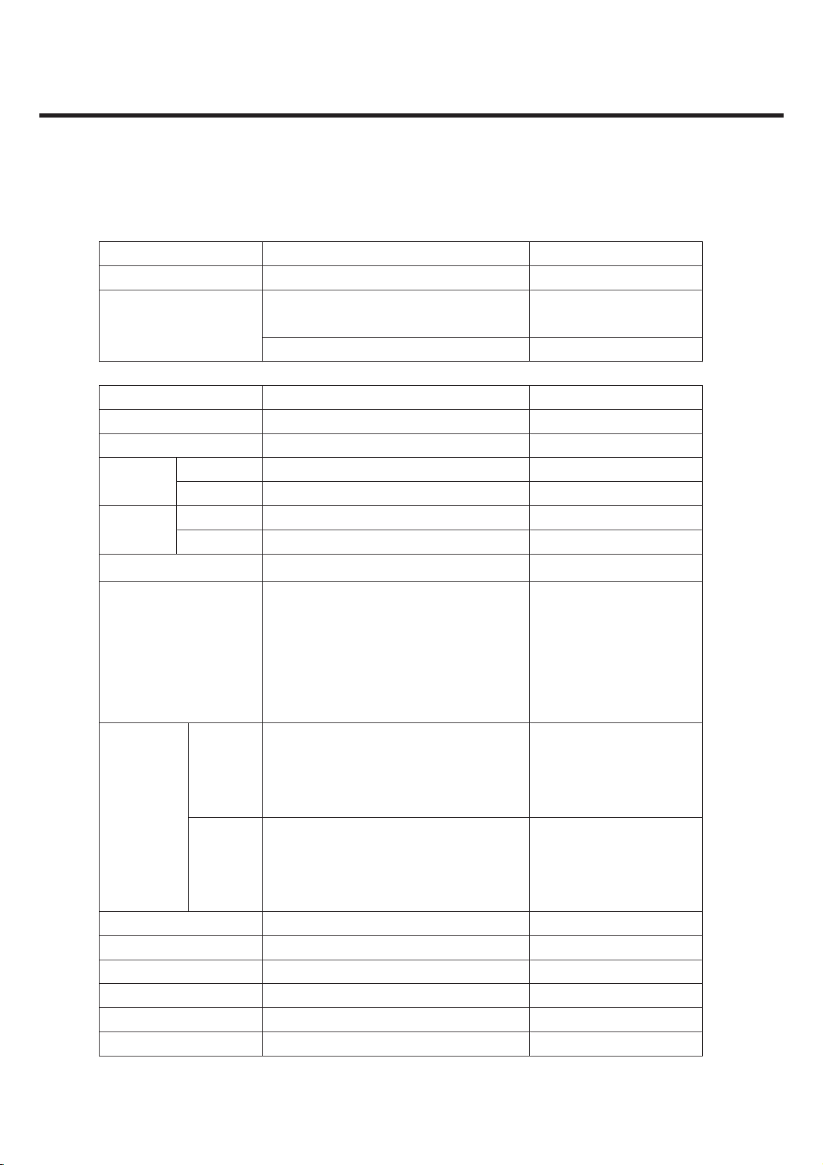
2.3 H/W features
Item Feature Comment
Form Factor Slide type
Battery
1)Capacity
Standard : Li-Ion, 900mAh
2) Packaging Type : Soft Pack
Item Feature Comment
Size 103 x 51.8 x 13.75
Weight 98 g With Battery
GSM 300 hours @paging period 5 Stand-by
time
WCDMA 300hours @DRX=7
GSM 240min @ Power Level 7 Talk
time
WCDMA 180min @Tx=12dBm
Charging time 3 hours @power OFF/900mAh
Rx sensitivity GSM850 : -105 dBm
EGSM900 : -105 dBm
DCS1800 : -105 dBm
PCS1900 : -105 dBm
WCDMA2100 : -106.7 dBm
WCDMA900 : -103.7 dBm
TX output
power
GSM/
GPRS
EDGE GSM850 : 27 dBm
GSM850 : 33 dBm
EGSM900 : 33 dBm
DCS1800 : 30 dBm
PCS1900 : 30 dBm
EGSM900 : 27 dBm
DCS1800 : 26 dBm
PCS1900 : 26 dBm
Class4 (GSM850)
Class4 (EGSM900)
Class1(DCS)
Class1(PCS)
E2 (EGSM850)
E2 (EGSM900)
E2 (DCS)
E2 (PCS)
GPRS compatibility GPRS Class 12
EDGE compatibility EDGE Class 12
Display 2.2” 240x320 (QVGA) TFT
Built-in Camera 3 Mega pixel
ANT Main : Internal Fixed Type
System connector 18 Pin
LGE Internal Use Only Copyright © 2009 LG Electronics. Inc. All right reserved.
- 10 -
Only for training and service purposes
GM310f service manual
Ear Phone Jack 3.5pi, 4 Pole, Stereo
PC synchronization Yes
Speech coding FR, EFR, HR, AMR
Vibrator Built in Vibrator
Blue Tooth V1.2, A2DP
2. PERFORMANCE
Voice Recording Yes
Speaker Phone
mode Support
Travel Adapter Yes
CDROM No
Stereo Headset Yes
Data Cable No
T-Flash Yes
Yes
Copyright © 2009 LG Electronics. Inc. All right reserved.
Only for training and service purposes
- 11 -
LGE Internal Use Only
2. PERFORMANCE
GM310f service manual
GM310f service manual
GM310f service manual
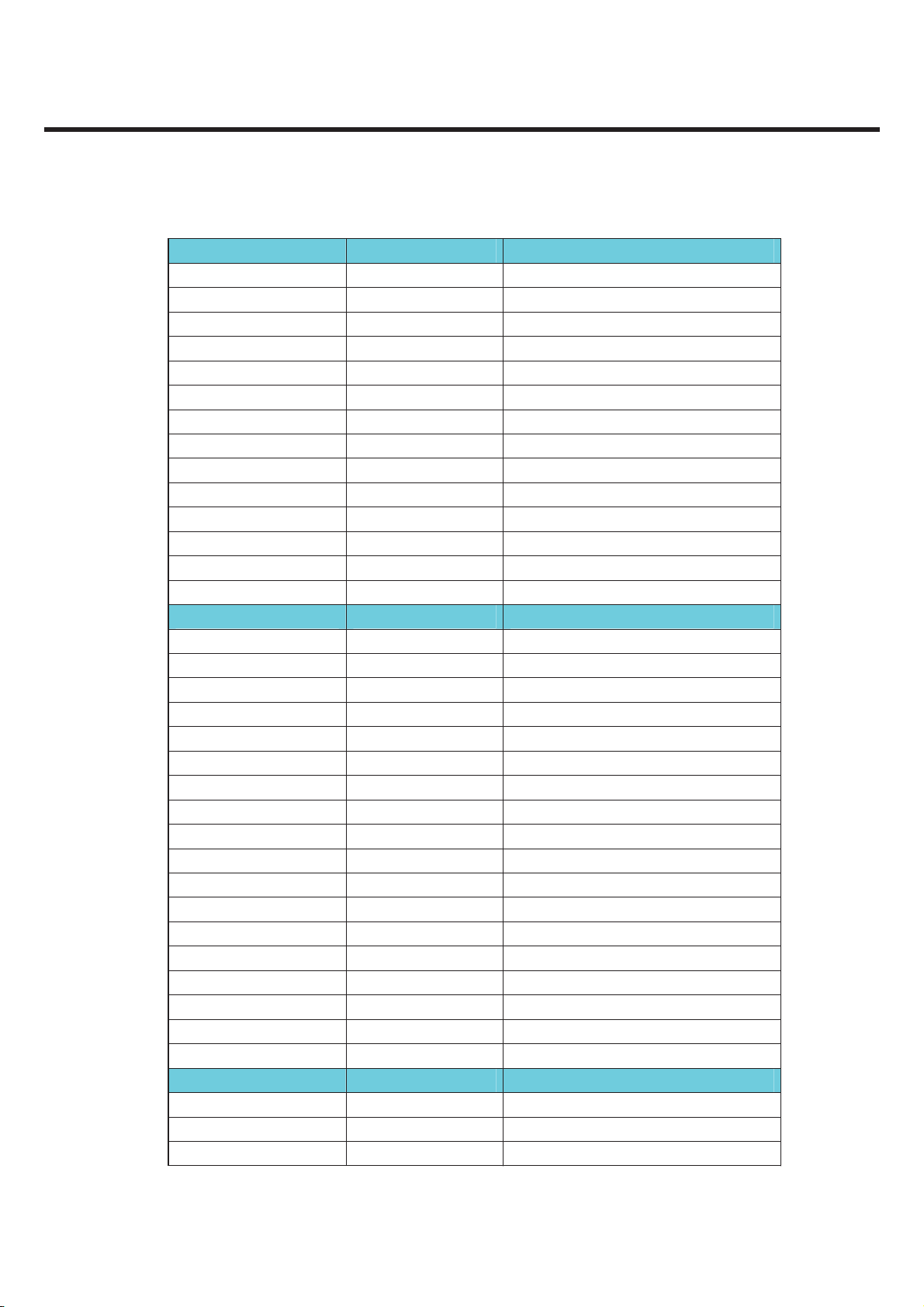
2.4 HW Spec.
2.4.1. GSM Transmitter/Receiver spec.
Item Specification
Frequency
Phase Error
Frequency Error
EMC(Radiated Spurious Emission
Disturbance)
Transmitter Output power and
Burst Timing
Burst Timing <3.69us
Spectrum due to modulation out
to less than 1800kHz offset
Spectrum due to modulation out
to larger than 1800kHz offset to
the edge of the transmit band
GSM850 TX : 824 - 849 MHz RX : 869 - 894 MHz
EGSM900 TX : 880 - 915 MHz RX : 925 - 960 MHz
DCS1800 TX : 1710 - 1785 MHz RX : 1805 - 1880 MHz
PCS1900 TX : 1850 - 1910 MHz RX : 1930 - 1990 MHz
Rms : 5°
Peak : 20 °
GSM : 0.1 ppm
DCS/PCS : 0.1 ppm
GSM/DCS : < -28dBm
GSM : 5dBm – 33dBm ± 3dB
DCS/PCS : 0dBm – 30dBm ± 3dB
200kHz : -36dBm
600kHz : -51dBm/-56dBm
GSM : 1800-3000kHz :< -63dBc(-46dBm)
3000kHz-6000kHz : <-65dBc(-46dBm)
6000kHz < : < -71dBc(-46dBm)
DCS : 1800-3000kHz :< -65dBc(-51dBm)
6000kHz < : < -73dBc(-51dBm)
Spectrum due to switching
transient
Reference Sensitivity – TCH/FS Class II(RBER) : -105dBm(2.439%)
Usable receiver input level range 0.012(-15 - -40dBm)
Intermodulation rejection –
Speech channels
AM Suppression
- GSM : -31dBm - DCS : 29dBm
Timing Advance ± 0.5T
400kHz : -19dBm/-22dBm(5/0), -23dBm
600kHz : -21dBm/-24dBm(5/0), -26dBm
± 800kHz, ± 1600kHz : -98dBm/-96dBm (2.439%)
-98dBm/-96dBm (2.439%)
LGE Internal Use Only Copyright © 2009 LG Electronics. Inc. All right reserved.
- 12 -
Only for training and service purposes
GM310f service manual
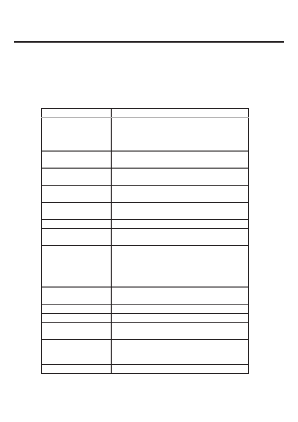
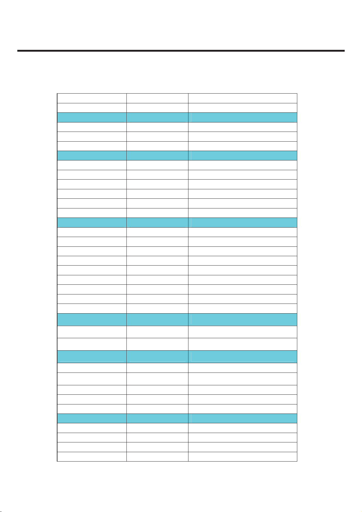
2.4.2. WCDMA Transmitter spec.
Item Specification
Transmit Frequency 1920 MHz ~ 1980 MHz/ 880 MHz ~ 915 MHz
Maximum Output Power +24 dBm / 3.84 MHz, +1 / -3 dB
Frequency Error within ±0.1 PPM
Open Loop Power Control Normal Conditions : within ±9 dB,
Extreme Conditions : within ±12 dB
Minimum Transmit Power < -50 dBm /3.84 MHz
Occupied Bandwidth < 5 MHz at 3.84 Mcps (99% of power)
2. PERFORMANCE
Adjacent Channel Leakage
Power Ratio (ACLR)
Spurious Emissions
|f-fc| > 12.5 MHz
Transmit Intermodulation < -31 dBc @ 5 MHz & < -41 dBc @ 10 MHz
Error Vector Magnitude < 17.5 %, when Pout ≥ -20 dBm
Peak Code Domain Error
> 33 dB @ ±5 MHz,
> 43 dB @ ±10 MHz
< -36 dBm / 1 kHz RW @ 9 kHz ≤ f < 150 kHz
< -36 dBm / 10 kHz RW @ 150 KHz ≤ f < 30 MHz
< -36 dBm / 100 kHz RW @ 30 MHz ≤ f < 1 GHz
< -30 dBm / 1 MHz RW @ 1 GHz ≤ f < 12.75 GHz
< -41 dBm / 300 kHz RW @ 1893.5 MHz < f < 1919.6 MHz
< -67 dBm / 100 kHz RW @ 925 MHz ≤ f ≤ 935 MHz
< -79 dBm / 100 kHz RW @ 935 MHz < f ≤ 960 GHz
< -71 dBm / 100 kHz RW @ 1805 MHz ≤ f ≤ 1880 MHz
when Interference CW Signal Level = -40 dBc
< -15 dB at Pout t -20 dBm
Copyright © 2009 LG Electronics. Inc. All right reserved.
Only for training and service purposes
- 13 -
LGE Internal Use Only
2. PERFORMANCE
GM310f service manual
A
2.4.3. WCDMA Receiver spec.
Item Specification
Receive Frequency 2110 ~ 2170 MHz / 925 ~ 960 MHz
Reference Sensitivity Level BER < 0.001 when Îor = -106.7 dBm / 3.84 MHz(WCDMA2100)
BER < 0.001 when Îor = -103.7 dBm / 3.84 MHz(WCDMA900)
Maximum Input Level BER < 0.001 when Îor = -25 dBm / 3.84 MHz
djacent Channel Selectivity
(ACS)
Blocking Characteristic BER < 0.001 when Îor = -103.7 dBm / 3.84 MHz(WCDMA2100)
Spurious Response BER < 0.001 when Îor = -103.7 dBm (WCDMA2100)
Intermodulation BER < 0.001 when Îor= -103.7 dBm / 3.84 MHz(WCDMA2100)
ACS > 33 dB where BER < 0.001 when Îor = -92.7 dBm / 3.84
MHz & Ioac = –52 dBm / 3.84 MHz @ ±5 MHz(WCDMA2100)
ACS > 33 dB where BER < 0.001 when Îor = -89.7 dBm / 3.84
MHz & Ioac = –52 dBm / 3.84 MHz @ ±5 MHz(WCDMA900)
when Îor = -100.7 dBm/ 3.84 MHz(WCDMA900)
& Iblocking = -56 dBm / 3.84 MHz @ Fuw(offset) = ±10 MHz
or Iblocking = -44 dBm / 3.84 MHz @ Fuw(offset) = ±15 MHz
when Îor = -100.7 dBm (WCDMA900)
& 3.84 MHz & Iblocking = -44 dBm
when Îor= -100.7 dBm / 3.84 MHz(WCDMA900)
& Iouw1 = -46 dBm @ Fuw1(offset) = ±10 MHz
& Iouw2 = -46 dBm / 3.84 MHz @ Fuw2(offset) = ±20 MHz
Spurious Emissions < -57 dBm / 100 kHz BW @ 9 kHz ≤ f < 1 GHz
< -47 dBm / 1 MHz BW @ 1 GHz ≤ f ≤ 12.75 GHz
Inner Loop Power Control In
Uplink
Adjust output(TPC command)
cmd 1dB 2dB 3dB
+1 +0.5/1.5 +1/3 +1.5/4
0 -0.5/+0.5 -0.5/+0.5 -0.5/+0.5
-1 -0.5/-1.5 -1/-3 -1.5/-4
group(10equal command group)
+1 +8/+12 +16/+24
LGE Internal Use Only Copyright © 2009 LG Electronics. Inc. All right reserved.
- 14 -
Only for training and service purposes
3. BB Circuit Technical brief
GM310f service manual
Φ
Fu
F
N
3. BB Circuit Technical brief
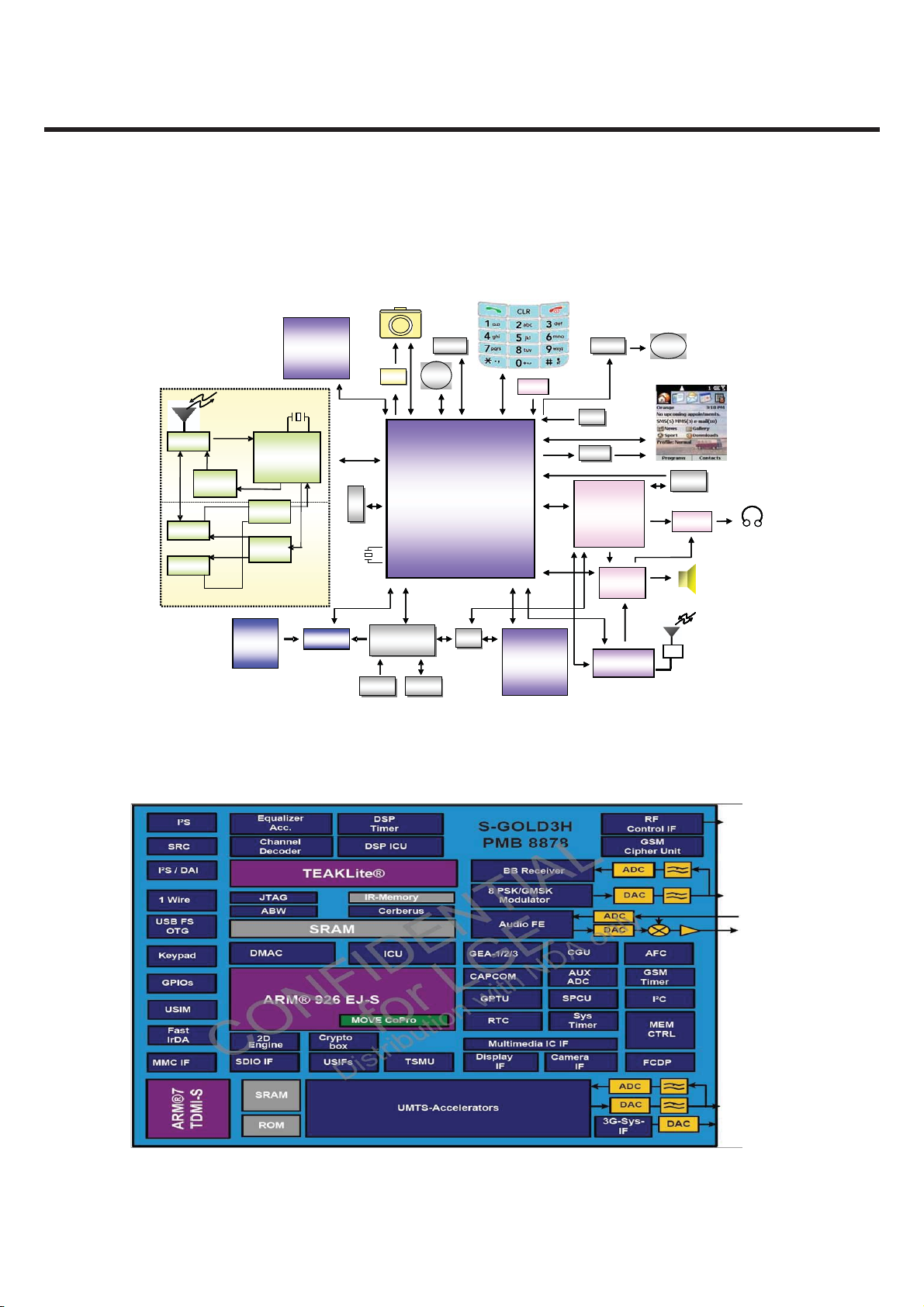
3.1 Functional Block Diagram
3M Camera
3M Camera3M Camera
Memory
Memory
Memory
1Gb Nand
1Gb Nand
1Gb Nand
512Mb SDRam
512Mb SDRam
LDO
LDO
LDO
RF Part
RF Part
RF Part
FEM
FEM
FEM
EDGE
UMTS 1900 or 2100
UMTS 1900 or 2100
UMTS 1900 or 2100
Duplex
Duplex
Duplex
Duplex
Duplex
Duplex
UMTS 850 or 900
UMTS 850 or 900
UMTS 850 or 900
GSM/EDGE 850/900/1800/1900
GSM/EDGE 850/900/1800/1900
GSM/EDGE 850/900/1800/1900
Transceiver
Transceiver
Transceiver
Transceiver
PMB6952
PMB6952
PMB6952
PMB6952
EDGE
EDGE
EDGE
PAM
PAM
PAM
UMTS
UMTS
UMTS
LNA
LNA
LNA
UMTS
UMTS
UMTS
UMTS
PAM
PAM
PAM
UMTS
UMTS
BATTERY
BATTERY
BATTER
900mAh
900mAh
Y
26M
26M
26M
Charging IC
Charging IC
ISL9221
ISL9221
U
LDO
BaseBand Processor
USIM
USIM
USIM
USIM
32K
32K32K
18Pin-MMI
18Pin-MMI
18Pin-MMI
18Pin-MMI
Connector
Connector
Connector
Connector
18Pin-MMI
TA
TA
TA
TA
Sub Keypad
Sub Keypad
Touch IC
Touch IC
Touch IC
Touch IC
Backup
Backup
Battery
Battery
PMB8868
BaseBand Processor
BaseBand Processor
PMB8868
PMB8868
USB
USB
USB
USB
Navi Key
Navi Key
High speed USB
High speed USB
Switch
Switch
Switch
Switch
Main Keypad
Main Keypad Main Keypad
PMB6821
Full speed USB
Full speed USB
Mic
Mic
PMIC
PMIC
PMIC
PMB6821
PMB6821
Motor IC
Motor IC
Motor IC
Motor IC
Hall IC
Hall IC
Hall IC
Hall IC
Charge
Charge
Charge
Charge
Pump
Pump
Pump
Pump
MP3 Chip
MP3 Chip
MP3 Chip
TCC8121
TCC8121
TCC8121
Audio Amp
Audio Amp
LM49150
LM49150
Audio
FM Recording
FM Recording
BT / FM Radio
BT / FM Radio
RBCA-B561A
RBCA-B561A
BT / FM
Motor
Motor
QVGA LCD(240 x 320)
QVGA LCD(240 x 320)QVGA LCD(240 x 320)
Micro SD
Micro SD
Micro SD
Micro SD
Switch
Switch
RCV/SPK
RCV/SPKRCV/SPK
Filter
FilterFilter
3.5
3.5
Φ
Φ
3.5
Ear-phone
Ear-phone
[Figure 3.1] Functional Block Diagram
3.2 Baseband Processor Introduction
[Figure 3.2] T op level block diagram of the MPEH(PMB8868)
Copyright © 2009 LG Electronics. Inc. All right reserved.
Only for training and service purposes
- 15 -
LGE Internal Use Only

3. BB Circuit Technical brief
GM310f service manual
3.2.1 General description
S-GOLD3H-LC is a HSDPA/WCDMA/EDGE/GPRS/GSM system in package solution consisting of a
mixed signal baseband IC with a 3G coprocessor IC.
l Baseband IC containing all analog and digital functionality of a cellular radio. Additionally S-
GOLD3
as a single chip solution, integrating the digital and mixed signal portions of the base band in 0.09um,
1.2V technology.
application (up to class 12), EGPRS (up to class 12) and DTM(class11) without additional external
hardware.
TM
Provides multimedia extensions such as camera, software MIDI, MP3 sound. It is designed
The chip will support the FR, EFR, HR and AMR-NB vocoding.
S-GOLD3
TM
support multi-slot operation modes HSCSD (up to class 10), GPRS for high speed data
3.2.2. Block Description
z Processing core
ARM926EJ-S 32 bit processor core for controller functions. The ARM926EJ-S includes an MMU,
and the Jazelle Java extension for Java acceleration.
- TEAKLite DSP core
z ARM-Memory
- 32k Byte Boot ROM on the AHB
- 128k Byte SRAM on the AHB, flexibly usable as program or data RAM
- 32k Byte Instruction Cache
- 32k Byte Data Cache
- 8k Byte Instruction Tightly coupled Memory(I-TCM)
- 8k Byte Data tightly coupled memory (D-TCM)
z DSP-Memory
- 120k x 16bit Program ROM
- 8k x 16bit Program RAM
- 72k x 16bit Data ROM
- 48k x 16bit Data XRAM
-5k x 16bit Data YRAM
- Incremental Redundancy(IR) Memory of 35904 words of 16bit
LGE Internal Use Only Copyright © 2009 LG Electronics. Inc. All right reserved.
- 16 -
Only for training and service purposes

3. BB Circuit Technical brief
GM310f service manual
z Shared Memory Block
1.5K x 32bit Shared RAM(dual ported) between controller system and TEAKLite.
z Controller Bus system
The processor cores and their peripherals are connected by powerful buses.
-Multi-layer AHB for connecting the ARM and the other master capable building blocks with the
internal and external memories and with the peripheral buses.
-An FPI-Bus for connecting GSM peripherals, called hereafter FPI3 bus.
-A controller FPI bus for connecting the low performance controller peripherals such as keypad,,
Called hereafter fPI2 bus.
-FPI2 and FPI3 are connected asynchronously to the AHB buses.
z Clock system
The clock system allows widely independent selection of frequencies for the essential parts of the S-
GOLD3H-LC. Thus power consumption and performance can be optimized for each application.
z Functional Hardware block
- CPU and DSP Timers
- MOVE coprocessor performing motion estimation for video encoding algorithms
(H.263, MPEG-4)
- Programmable PLL with additional phase shifters for system clock generation
- GSM Timer Module that off-loads the CPU from radio channel timing
- GMSK / 8-PSK Modulator according to GSM-standard 05.04 (5/2000)
- GMSK Modulator: gauss-filter with B*T=0.3
- EDGE Modulator: 8PSK-modulation with linearized GMSK-Pulse-Filter
- Hardware accelerators for equalizer and channel decoding.
- Incremental Redundancy memory for EDGE class 12 support
- A5/1, A5/2, A5/3 Cipher unit
- GEA1, GEA2, GEA3 Cipher Unit to support GPRS data transmission
- Advanced static and dynamic power management features including TDMA-Frame
synchronous low power mode and enhanced CPU modes(idle and sleep modes)
Copyright © 2009 LG Electronics. Inc. All right reserved.
Only for training and service purposes
- 17 -
LGE Internal Use Only
3. BB Circuit Technical brief
GM310f service manual
3.2.3 RF Interface(T_OUT)
S-Gold3H-LC uses this interface to control RF IC and Peripherals.
[Table 3.2.3-1] RF Interface Spec.
T_OUT
Resource Interconnection Description
T_OUT0 TXON_PA PAM Power on
T_OUT1 -
T_OUT2 ANT_SEL1 FEM control
T_OUT3
T_OUT4
T_OUT5
T_OUT6 PA_MODE PAM Mode select
T_OUT7 ANT_SEL2 FEM control
T_OUT8 ANT_SEL3 FEM control
T_OUT9
T_OUT10
LGE Internal Use Only Copyright © 2009 LG Electronics. Inc. All right reserved.
- 18 -
Only for training and service purposes
GM310f service manual
3.2.4 ADC channel
3. BB Circuit Technical brief
ADC block is composed of 11 external ADC channel. This block operates charging process and other
related process by reading battery voltage and other analog values.
[Table 3.2.4-1] S-Gold3 ADC channel usage
ADC channel
Resource Interconnection Description
M0 BAT_ID Battery temperature measure
M1 RF_TEMP RF block temperature measure
kM2 N.C
M3 JACK_TYPE Accessory type detect
M4 N.C
M5 N.C
M6 N.C
M7 H/W VERSION H/W version detect
M8 VBAT Battery supply voltage measure
M9 N.C
M10 N.C
Copyright © 2009 LG Electronics. Inc. All right reserved.
Only for training and service purposes
- 19 -
LGE Internal Use Only
3. BB Circuit Technical brief
GM310f service manual
GM310f service manual
3.2.5 GPIO map
Over a hundred allowable resources, GM310 is using as follows except dedicated to SIM and Memory.
GM310 GPIO(General Purpose Input/Output) Map, describing application, I/O state, and enable level,
is shown in below table
[Table 3.2.5-1] S-Gold3H-LC GPIO pin Map
Port Function Net Name Description
KEY MATRIX
KP_IN0
KP_IN1
KP_IN2
KP_IN3
KP_IN4
KP_IN5
KP_IN6
KP_OUT0
KP_OUT1
KP_OUT2
KP_OUT3
USIF1
USIF1_RXD_MRST
USIF1_TXD_MTSR
USIF1_RTS_N
USIF1_CTS_N
USIF2
USIF2 _RXD_MRST
USIF2 _TXD_MTSR
USIF2_RTS_N
USIF2_CTS_N
USIF3
USIF3 _RXD_MRST
USIF3 _TXD_MTSR
GPIO_21
CLK
CLK32K
GPIO_22
KEYIN0
KEYIN1
KEYIN2
KEYIN3
KEYIN4
KEYIN05
KEYOUT5
KEYOUT0
KEYOUT1
KEYOUT2
KEYOUT3
UART_RX UART Data
UART_TX UART Data
USB_ DAT_VP USB Data
USB_SE0_VM USB Data
TCC_PWRON Multimedia chip power on
TCC_RESET Multimedia chip reset
BT_UART_RTS Bluetooth RTS
BT_UART_CTS Bluetooth CTS
BT_UART_RX Bluetooth UART Data
BT_UART_TX Bluetooth UART Data
USB_SEL USB 1.1, 2.0 select
CLK32k For FM Radio, BT CLK32K
Not used
LGE Internal Use Only Copyright © 2009 LG Electronics. Inc. All right reserved.
- 20 -
Only for training and service purposes
GM310f service manual
CAMERA I/F
CIF_D0
CIF_D1
CIF_D2
CIF_D3
CIF_D4
CIF_D5
CIF_D6
CIF_D7
CIF_PCLK
CIF_HSYNC
CIF_VSYNC
CLKOUT2
CIF_PD
CIF_RESET
LCD I/F
DIF_D0
DIF_D1
DIF_D2
DIF_D3
DIF_D4
DIF_D5
DIF_D6
DIF_D7
DIF_D8
DIF_CS1
EINT4
DIF_CD
DIF_WR
LCD_RD
DIF_HD
DIF_VD
DIF_RESET1
DIF_RESET2
I2C
I2C1_SCL
I2C1_SDA
PM_INT (EINT)
3. BB Circuit Technical brief
CAM_D0 Camera DATA[0]
CAM_D1 Camera DATA[1]
CAM_D2 Camera DATA[2]
CAM_D3 Camera DATA[3]
CAM_D4 Camera DATA[4]
CAM_D5 Camera DATA[5]
CAM_D6 Camera DATA[6]
CAM_D7 Camera DATA[7]
CAM_PCLK Camera pixel clock
CAM_HSYNC Camera H sync
CAM_VSYNC Camera V sync
CAM_MCLK Camera main clock
CAM_PWR_EN Camera power down(active high)
CAM_RESET Camera reset
LCD_D0 LCD data[0]
LCD_D1 LCD data[1]
LCD_D2 LCD data[2]
LCD_D3 LCD data[3]
LCD_D4 LCD data[4]
LCD_D5 LCD data[5]
LCD_D6 LCD data[6]
LCD_D7 LCD data[7]
DIF_ID LCD data[8]
_LCD_CS1 LCD chip select
EXT_SPK_DETECT External speaker detect
LCD_CD Command Data switch
_LCD_WR LCD Write
LCD_RD LCD Read
HOOK_DETECT Headset hook detect
LCD_VSYNC LCD Vsync
_LCD_RESET LCD Reset
A_RESET 3G reset
SCL_PMIC For PMIC
SDA_PMIC For PMIC
PM_INT For PMIC
Copyright © 2009 LG Electronics. Inc. All right reserved.
Only for training and service purposes
- 21 -
LGE Internal Use Only
3. BB Circuit Technical brief
GM310f service manual
I2C2_SCL
I2C2_SDA
SIM I/F
CC_IO
CC_CLK
CC_RST
I2S2
GPIO_31
GPIO_102
GPIO_32
CC0CC7IO
GPIO_34
GPIO_103
External Memory
GPIO_104
GPIO_105
GPIO_106
GPIO_39
GPIO_40
GPIO_41
GPIO_22
GPIO_107
GPIO_108
SCL
SDA
SIM_IO SIM CARD DATA
SIM_CLK SIM CARD CLOCK
SIM_RST SIM CARD RESET
BT_RESETn Bluetooth Reset
DBB_BT_INT S-GOLD3H-LC to Bluetooth interrupt
TCC_INT Multimedia chip Interrupt
BT_INT Bluetooth to S-GOLD3H-LC interrupt
MAIN_KEY_EN Number Key LED enable
Not used
TOUCH_RESET Touch IC Reset
SDA_TOUCH Touch IC I2C Data
SCL_TOUCH Touch IC I2C Clock
TCC_MMC_DETECT Multimedia chip T-flash detect
CAM_LDO_EN Camera LDO enable
TOUCH_WAKEUP Touch IC wakeup
TOUCH_INT Touch IC Interrupt
MOTOR_EN Vibrator enable
Not used
IrDA
GPIO_110
GPIO_111
I2S1
I2S1_CLK0
I2S1_CLK1
I2S1_RX
I2S1_TX
I2S1_WA0
Audio I/F
EPN1
EPP1
EPPA1
EPREF
LGE Internal Use Only Copyright © 2009 LG Electronics. Inc. All right reserved.
USB_OEn For USB
SLIDE_DETECT Slide on/off detect
BT_PCM_CLK For Bluetooth
BT_PCM_RX For Bluetooth
BT_PCM_TX For Bluetooth
BT_PCM_SYNC For Bluetooth
REC_N For Receiver
REC_P For Receiver
HS_L For Headset
Reference
- 22 -
Only for training and service purposes
3. BB Circuit Technical brief
GM310f service manual
EPPA2
MICN1
MICP1
MICN2
MICP2
VMICP
VMICN
ADC
M0
M1
M2
M3
M7
M8
M9
M10
Reference
VREF
IREF
JTAG I/F
JTAG0_TDO
JTAG0_TDI
JTAG0_TMS
JTAG0_TCK
JTAG0_TRST_n
JTAG0_RTCK
JTAG1_TDO
JTAG1_TDI
JTAG1_TMS
JTAG1_rTCK
JTAG0_TRST_n
ETM I/F
TRIG_IN
MON1
MON2
TRACESYNC
TRACECLK
PIPESTAT[2]
HS_R For Headset
MAIN_MIC_N For Main Mic
MAIN_MIC_P For Main Mic
HS_MIC_N For Headset Mic
HS_MIC_N For Headset Mic
VMIC_P Power for MIC
GND Ground for MIC
BAT_ID Battery temperature measure
RF_TEMP RF block temperature measure
JACK_TYPE Accessory type detect
H/W VERSION H/W version detect
VBAT Battery supply voltage measure
VREFN
GND with resistor
MON1 ETM
MON2 ETM
Copyright © 2009 LG Electronics. Inc. All right reserved.
Only for training and service purposes
- 23 -
LGE Internal Use Only
3. BB Circuit Technical brief
GM310f service manual
PIPESTAT[1]
PIPESTAT[0]
TRACEPKT[0]
TRACEPKT[1]
TRACEPKT[2]
TRACEPKT[3]
TRACEPKT[4]
TRACEPKT[5]
TRACEPKT[6]
TRACEPKT[7]
Memory
MEM_AD[0]
MEM _AD[1]
MEM _AD[2]
MEM _AD[3]
MEM _AD[4]
MEM _AD[5]
MEM _AD[6]
MEM _AD[7]
MEM _AD[8]
MEM _AD[9]
MEM _AD[10]
MEM _AD[11]
MEM _AD[12]
MEM _AD[13]
MEM _AD[14]
MEM _AD[15]
MEM _WR_n
MEM _RD_n
MEM _BC0_n
MEM _BC1_n
MEM _BC2_n
MEM _BC3_n
MEM _A[0]
MEM _A[1]
MEM _A[2]
MEM _A[3]
MEM _A[4]
DATA(0)
DATA(1)
DATA(2)
DATA(3)
DATA(4)
DATA(5)
DATA(6)
DATA(7)
DATA(8)
DATA(9)
DATA(10)
DATA(11)
DATA(12)
DATA(13)
DATA(14)
DATA(15)
_WR
_RD
_BC0
_BC1
LDQS
UDQS
ADD(0)
ADD(1)
ADD(2)
ADD(3)
ADD(4)
LGE Internal Use Only Copyright © 2009 LG Electronics. Inc. All right reserved.
- 24 -
Only for training and service purposes
3. BB Circuit Technical brief
GM310f service manual
MEM _A[5]
MEM _A[6]
MEM _A[7]
MEM _A[8]
MEM _A[9]
MEM _A[10]
MEM _A[11]
MEM _A[12]
MEM _A[13]
MEM _A[14]
MEM _A[15]
MEM _A[16]
MEM _A[17]
MEM _A[18]
MEM _A[19]
MEM _A[20]
MEM _A[21]
MEM _A[22]
MEM _A[23]
MEM _A[24]
MEM _A[25]
MEM _A[26]
MDM_SDA[11]
MDM_SDA[12]
MDM_SDA[13]
MDM_SDA[14]
MEM _CS0_n
MEM _CS1_n
MEM _CS2_n
MEM _CS3_n
MEM _ADV_n
MEM _RAS_n
MEM _CAS_n
MEM _WAIT_n
MEM _SDCLK0
MEM _BFCLK01
MEM _BFCLK02
MEM _CKE
ADD(5)
ADD(6)
ADD(7)
ADD(8)
ADD(9)
ADD(10)
ADD(11)
ADD(12)
ADD(13)
ADD(14)
ADD(15)
ADD(16)
ADD(17)
ADD(18)
ADD(19)
ADD(20)
ADD(21)
ADD(22)
ADD(23)
ADD(24)
ADD(25)
ADD(26)
ADD(27)
ADD(28)
ADD(29)
ADD(30)
_NAND_CS INTEL NOR (64MB)
_RAM_CS INTEL SDRAM (64MB)
_CS3
ADV_A15
_RAS
_CAS
_WAIT
SDCLKO For Burst mode
BFCLKO For Burst mode
SDCLK1 For Burst mode
CKE
Copyright © 2009 LG Electronics. Inc. All right reserved.
Only for training and service purposes
- 25 -
LGE Internal Use Only
3. BB Circuit Technical brief
GM310f service manual
Memory
FCDP_RBn
GPIO_60
TDMA I/F
T_OUT0
T_OUT1
T_OUT2
GPIO_46
EINT6
CC0CC2IO
T_OUT6
T_OUT7
T_OUT8
GPIO_52
CC1CC7IO
GPIO_54
GPIO_55
RF I/F
RF_STR0
CC1CC5IO
RF_DATA
RF_CLK
RF_LOCK_DET
MASTER_ON
PA_MODE
FEM_CTRL[0]
FEM_CTRL[1]
FEM_CTRL[2]
System Port
AFC
CLKOUT0 [<=26MHz]
F26M
F32K
OSC32K
RESET_n
TRIG_OUT
RTC_OUT
VCXO_EN
FCDP
RPWRON_DBB
TXON_PA PAM
ANT_SEL1
LCD_BL_CTRL Charge pump control
_EOC Charging terminate signal
MMC_DETECT SD card detect
PA_MODE PAM
ANT_SEL2
ANT_SEL3
DSR
JACK_DETECT Jack detect
TA_DETECT Charger detect
CHG_EN Charging enable
2G_EN
_PPR Charger detect
2G_DATA
2G_CLK
3G_LD
3G_MASTER_ON
3G_PA_MODE1
ANT_SEL4
ANT_SEL5
ANT_SEL6
AFC
Not used
26MHZ 26M Main Clock
to 32k crystal
to 32k crystal
_RESET
TRIG_OUT
RTC_OUT
VCXO_EN
LGE Internal Use Only Copyright © 2009 LG Electronics. Inc. All right reserved.
- 26 -
Only for training and service purposes

GM310f service manual
DSP
GM310f service manual
DSPIN0
3. BB Circuit Technical brief
CLK32K
DSPOUT1
GPIO_63
WDOG Navi key LED Backlight Control
HS_MIDI_EN Headset MIDI enable
3.3 Power management IC
3.3.1 General Description
SM-POWER is a highly integrated Power and Battery Management IC for mobile handsets. It has
been specially designed for usage with S-Gold3. Although optimized for usage with the Infineon
SGOLD
baseband device it is suitable for the S-GOLD lite and the E-GOLD+ baseband devices as well.
It also supports the cellular RF devices like SMARTi-DC, SMARTi-DC+, SMARTi-SD and the
Bluemoon Single, Infineon’s single chip solution for Bluetooth. If used with S-GOLD3 it provides all
power supply functions (except for the RF PA) for a complete advanced GSM Edge smart phone
minimizing external device count.
Block Description
• Highly efficient step-down converter for main digital baseband supply including Core, DSP and
memory interface (External Bus Unit).
• Support of S-GOLD standby power-down concept
• Low-drop-out (LDO) regulators for Flash and mobile RAM memory devices
• Voltage independent switching of two SIM cards
• LDO regulators for baseband I/O supply
• LDO regulator for analog mixed-signal section of S-GOLD
• Low-noise LDO regulators for RF devices
• Supply for Bluemoon Single, Infineon’s single chip solution for Bluetooth
• Audio amplifier 8 Ohms for handsfree operation and ringing
• Charge Control for charging Li-Ion/Polymer batteries under software control
• Pre-charge current generator with selectable current level
• RTC regulator with ultra-low quiescent current
• USB interface support for peripheral and mini-host mode
• Backlight LEDs driver with current selection and PWM dimming function
• Two single LED driver outputs for signaling
Copyright © 2009 LG Electronics. Inc. All right reserved.
Only for training and service purposes
- 27 -
LGE Internal Use Only

3. BB Circuit Technical brief
GM310f service manual
• Vibrator driver with adjustable voltage
• Fully controlable by software via I2C - Bus
• Temperature and battery voltage sensors
• Interrupt channels for peripherals
• System debug mode
• VQFN 48 package with heat sink and non-protruding leads
• Compatible with the Infineon E-GOLD+ V2 and V3
SM-POWER is a further step on the successful E-Power product line with enhanced and optimized
functionality.
SM-POWER features a baseband supply concept with a DC/DC step-down converter cascaded by
two linear regulators
- SM-POWER’s DC/DC converter makes up to 40 % reduction of battery current for smart phone
functions (e.g. organizer functions, games, MP3 decoding) possible.
- SDBB has high efficiency up to 95% and also a power save mode.
- Memory Interface is directly supported by the SDBB
- SDBB can also act as main supply voltage for E-GOLD+ or S-GOLDlite baseband devices.
- For S-GOLD two linear regulators for DSP and Core are cascaded after the SDBB.
SM-POWER supports the standby power-down concept of S-GOLD by temporarily switching off the
linear regulator for the DSP during mobile standby whenever this subsystem is not used. In this phase
the ARM controller and most peripherals including parts of the on-chip SRAM are kept powered-up
withpower being supplied by the other linear regulator.
SM-POWER includes a fully differential audio amplifier able to drive loads down to a nominal value of
8 Ohm for usage in hands-free phones and for ringing
- 450 mW maximum output power
- adjustable gain
- mute switch SM-POWER also integrates a charging function for Li-Ion, Li-Polymer batteries
- click and pop -protection SM-POWER also integrates a charging function for Li-Ion, Li-Polymer
batteries
- Precharge current source with two current levels
- Constant current / constant voltage charging with 3 different termination voltages
- Programable charge current limitation for use with different batteries
- Freely programable pulse charging to reduce the thermal power dissipation in the constant voltage
charging phase
LGE Internal Use Only Copyright © 2009 LG Electronics. Inc. All right reserved.
- 28 -
Only for training and service purposes

3. BB Circuit Technical brief
GM310f service manual
- Top-off charge current sensing SM-POWER completes the USB interface of S-GOLD
- Regulated voltage for S-GOLD USB interface including reverse current and overvoltage protection
- Switch to supply USB pull-up resistor
- Mini-host pull down resistor functionality
- Charge pump with internal switching capacitor for USB host VBUS supply voltage SM-POWER fully
supports LED and Vibra Motor functionality
- no external components needed
- driver for backlight LEDs adjustable in steps up to 140mA and with soft turn on and off by PWM
dimming
- two driver outputs for single LEDs for precharge indication and signaling with i.e. change of colour
- driver for Vibra Motor with adjustable voltages, soft startup / shutdown and current limitation
SMPOWER
offers several control functions
- Power-on Reset Generator with logic state machine
- I2C bus interface
- I2C bus configurable mode control logic with ON (push-button or RTC), VCXOEN and LRF3EN
(wake-up by Bluetooth) inputs
- Programable interrupt channels to handle peripherals like SIM, MMC and USB
- Monitoring of charging functions
- Undervoltage Shut-Down
- Errorflags (volatile or non-volatile) from many power-supply functions and thermal sensor in order to
debug system
- Overtemperature Shut-Down
- Overtemperature Warning
- Support of S-GOLD standby power-down concept
- Support of S-GOLD Power-Down Pad Tristate Function
Copyright © 2009 LG Electronics. Inc. All right reserved.
Only for training and service purposes
- 29 -
LGE Internal Use Only
3. BB Circuit Technical brief
GM310f service manual
[Table 3.3.1-1] LDO Output Table of SM-Power3
LDO Net name Output Voltage Output Current Usage
SD1 1V35_Core 1.35V 600mA Core & for LDO
SD2 1V8_SD 1.8V 300mA Memory
VAUX 2V85_VFM 2.85V 100mA SUB PMIC
VIO 2V62_VIO 2.62V 100mA Peripherals
VSIM 2V9_SIM 2.9V 70mA SIM card
VMME 2V9_VMME 2.9V 150mA u-SD
VUMTS 2V85_VCD 2.85V 110mA LCD
VAUDIOa 2V5_VAUDA 2.5V 200mA Stereo headset, Mono earpiece
VAUDIOb 2V5_VAUDB 2.5V 50mA Analog parts of S-Gold
VRF1 2V85_VRF 2.85V 150mA
2.85 V supply for SMARTi-PM
RF transceiver
1.5 V supply for SMARTi-PM
VRF2 1V5_VRF 1,53V 100mA
RF transceiver
VRF3 2V855_VBT 2.7V 150mA Bluetooth
VPLL 1V35_VPLL 1.35V 30mA S-GOLD3H PLL
VRTC 2V11_RTC 2.11V 4mA Real Time Clock
VAFC 2V7_VRF 2.65V 5mA Not used
VVIB 2V8_VAMP 2.8V 140mA Not used
OIV_26V
TP203
K3
OUTPORT
POWER_ON
VSS24
VSS25
G8
TP204
L3
G9
WDOG
K4
WDOG
VSS26
H5
PWRON
ON_OFF2
TP205
L5
ON_OFF1L4ON_OFF2
VSS27
VSS28
H6
H7
SPOWER_INT
RESOURCE_CTRL
K5
J5
I2C_INT
ON_OFF_OUT
RESOURCE_CRTL
VSS30
VSS29
J6
SDA_PMIC
K6
I2C_DAT
2
202R
K7.4
SCL_PMIC
J7
I2C_CLK
H8
L6
VSS_SD1
H4
02R
BL1
BL2
K7
BL1_PWM
BL2_PWM
VSS_SD2D9VSS_VREF
K7.4
3
J8
BL3
BL3_PWM
L7
CH_CNTRL
L8
K8
CHARGE_UC
CH_SOURCE
K9
L9
K10
SENSE_IN1
VDD_CHARGE
TABV
C
J9
VDD_REF
SENSE_IN2
V133RDK
2
3
402C
1
u1
102
D
502C
u33
1.0112
u
102
L
TP206
Hu01
A8
VLED
D202
L11
VSD1
S
RB521S-30
C
EMMV
01C
EMMDDV
01D
DV
2FRD
11
D
2FRV
01E
3FRV
11E
FA_31FRDDV
C
01F
RV
1F
11
F
BIVV
1
1G
BIVMISDDV
01G
MISV
11H
CFAV
01H
CTRV
202BF
9H
STMUDDV
11J
STMUV
BF_1DS
302BF
11K
1DSDDV
01
J
01L
806
1
LBF_1D
912C
u7.4
806
1
HCV_PVO
G
602
R
BSUV_PVO
K7
4
TCETED_AT
012
R
K74
EROC_53V1
DCLV_58V2
TABV
1608
1608
1608
1608
4.7u
2.2uC228
C216 10u
C229
C230 4.7u
CTR_11V2
1608
1608
10u
132C332
C
C217
C220 10u
u
1
1
u
CIMP
R
BDUAV_5V2
DS_8V
1
ADUAV_5V2
412C
312C
2
u2.
u2.
2
122C
322
0
C
C
u1.
222
u01
u01
806
8061
1
702R
2FFO_NOTUO_CT
K72
902
R
D
IN
nEO_BSU
PV_TAD_BSU
MV_0ES_
BSU
ABV
T
MFV_58V2
P
102B
F
8061
B
5
12C
u
1
R
812C
u7.4
806
1
TABV
1B
2
C
3D 11
V
1
C
PD_SF_BSU
MD_SF_BSU
nTSRM
NE_OXCV_MP
NE_OXCV_T
302D
03-S125B
4
22C
u2.2
1
806
+D
2D
D
-
nTSRMP
3E
1
D
2E
1
E
2F
1
F
2G
1G
2H
1
H
1J
202L
2J
3
H
1
Hu0
3J
S
1K
2K
S
2
L
522C
u1.0
C226 2.2u
8061
C227 4.7u
BSUV
TAB
TABV
V
2.2u
102C
u2.
2
1
806
806
1
C202
C
412R
K00
1
0.1u
C210
C5
B6
A7
C4
B5
B7
A4
A3
B2
A2
B3
C3
AC-
DAT_VP
SE0_VM
VCR
NIPV
NIM
N_TESER
N_2TESER
N_1PEELS
N_2PEELS
AOIDUAV
AOIDUADDV
BOIDUADDV
BOIDUAV
XUAV
XUADDV
ETAG_1US
DNG_1US
BF_1US
ESNESI_1U
2DSDDV
BF_2D
BF_2DS
L
AC+
OE_N
SUSPEND
A5
VUSB
VDD_USB
MONO_INP
MONO_INN
VREFEX_M
VDD_MONO
MONO_OUTP
VSS1
VSS2
C6
D4
302
u1.0
C7
VSS_MONO
VSS3
D5
1
A6
MONO_OUTN
VSS4
VSS5
D6
D7
%
100KR215
B8
RREF
VSS6D8VSS7E4VSS8
C8
E5
1u
C212
VREF
E6
1
MAIN_KEY_LED
MAIN_KEY_EN
A9
B10
C9
FLASH_ON
FLASH_SHINK
VSS10
VSS11
VSS9
E7
E8
E9
53V
1u
C207
TXONPA
VSS12
F3
LLPV_
T
ABV
TABV
OIV_
2
26V
4.7KR211
2.2uC209
C208 2.2u
R213 4.7K
R212 4.7K
8061
TP202
J4
A1
A11
B4
B11
L1
A10
B9
VIO
VPLL
VSD2
PUMS1
PUMS2
PUMS3
VDDPLLIO
102U
1286BMP
VSS13
VSS14
VSS15
VSS16
VSS17
VSS18
VSS19
VSS20
VSS21
VSS22G5VSS23
F4
F5
F6
F7
F8
F9
G3
G4
G6
G7
FRV_7V2
2
u2.2
FRV_5V
8V2
FRV_5
M
2
ISV_9V
632C
532C
u
u2.2
2.2
EMMV_9V2
1
DS_8V
1
TBV_58V
0
42C
732
C432C
C
832
9
32C
u2.
2
u2.2
2.2
u
u2.2
[Figure3.3.1-1] SM-Power 3 Circuit Diagram
LGE Internal Use Only Copyright © 2009 LG Electronics. Inc. All right reserved.
- 30 -
Only for training and service purposes
GM310f service manual
3.3.2 Charging control
3. BB Circuit Technical brief
- GM310 is use external charging IC
-Charging IC is ISL9221
1. Charging method : CC-CV
2. Charger output voltage : 5.1 V
3. Charging time : 2h 10m
4. Charging current : 600 mA
5. CV voltage : 4.2 V
6. Cutoff current : 117 mA
7. Full charge indication current (icon stop current) : 117 mA
8. Recharge voltage : 4.15 V
9. Low battery alarm
a. Idle : 3.45 V ~ 3.31 V
b. Dedicated : 3.45 V ~ 3.3 V
10. Low battery alarm interval
a. Idle : 3 min
b. Dedicated : 1 min
11. Switch-off voltage : 3.31 V
12. Charging temperature adc range
a. ~ -20 : low charging voltage operation (3.℃ 6 V ~ 3.9 V) .
b. -20 ~ 60 : standard charging (up to 4.2 V) ℃℃
c
. 60 ~ : low charging voltage operation (3.6V ~ 3.9V) ℃
G
AHC
I G
C
NI
R
IV_26V2
O
R
722
1
K00
1
R
PP
_
COE_
NE_G
HC
GHCV_BSU
GHC
V
R_11V
C
2
T
8
22R
K00
752C
1
u
U
402
1
C
V
D
2
BSUV
3
_
RPP
4
GHC
_
5
NE_
6
NI
MI
852
C
9
R
2
2
u1
4
K7.
1
[Figure 3.3.2-1] Charging IC (ISL9221)
Copyright © 2009 LG Electronics. Inc. All right reserved.
Only for training and service purposes
- 31 -
V
T
AB
2
29LSI
1
3
1
D
NG
P
2
1
P
V
B_CD
Y
1
1
AB
T
0
1
U
P
B_BS
Y
9
DVI
C
8
NG
D
7
BSU
I
Am006Am711
Am873
132R
032
R
K81
3
K
11
.
%
1
1%
%
952C
1
u
u1
GHC
VO
V_P
BSUV_PVO
6
2
1
062C
C
1
u
LGE Internal Use Only
 Loading...