

LG GM210 Service Manual
Service Manual Model : GM210
Internal Use Only
Service Manual
GM210
Date: April, 2009 / Issue 1.0

Table Of Contents
1. INTRODUCTION ...............................................5
1.1 Purpose ......................................................................5
1.2 Regulatory Information .................................................5
1.3 Abbreviations ..............................................................7
2. SYSTEM SPECIFICATION.................................9
2.1 H/W Features ..............................................................9
2.2 Technical Specifi cation ...............................................11
3. TECHNICAL BRIEF .........................................16
3.1 Main Processor(Digital Part : AD6725, U102) ..............16
3.2 Main Processor (Analog Part : AD6725, U102) ............19
3.3 RF Transceiver (AD6546) ...........................................26
3.4 Power Amplifi er Module (SKY77523) ..........................39
3.5 BT Module with integrated FM tuner ...........................30
3.6 MEMORY(PF38F5060M0Y0BE, U100 ) .......................32
3.7 Multi-Media Processor (AIT817, U602) .......................35
3.8 SIM Card Interface .....................................................38
3.9 Micro-SD Card Interface ............................................39
3.10 LCD Interface ..........................................................40
3.11 Battery Charger Interface .........................................43
3.12 Keypad Interface .....................................................44
3.13 Audio Interface ........................................................46
3.14 Camera Interface(2M Fixed Focus Camera) ...............53
3.15 KEY BACLKLIGHT LED Interface ................................55
3.16 Vibrator Interface .....................................................57
4. TROUBLE SHOOTING ..................................... 58
4.1 RF Component ..........................................................58
4.2 RX Trouble ................................................................59
4.3 TX Trouble .................................................................64
4.4 Power On Trouble ......................................................68
4.5 Charging Trouble .......................................................71
4.6 Vibrator Trouble .........................................................73
4.7 LCD Trouble ..............................................................75
4.8 Camera Trouble .........................................................79
4.9 Speaker Trouble ........................................................83
4.10 Earphone Trouble .....................................................85
4.11 Receiver Trouble ......................................................89
4.12 Microphone Trouble .................................................91
4.13 SIM Card Interface Trouble .......................................93
4.14 KEY backlight Trouble ..............................................95
4.15 RTC Trouble ............................................................97
4.16 Folder on/off Trouble ................................................99
4.17 Micro SD Trouble ...................................................101
4.18 FM radio Trouble ...................................................103
5. DOWNLOAD .................................................105
5.1 Download................................................................105
6. BLOCK DIAGRAM ........................................111
7. CIRCUIT DIAGRAM ...................................... 113
8. BGA Pin Map .............................................. 121
9. PCB LAYOUT ...............................................125
10. Confi guration of HOT KIMCHI .................131
10.1 BB Test [MENU 1] ..................................................132
10.2 RF Test [MENU 2] ..................................................134
10.3 MF mode [MENU 3] ...............................................134
10.4 Trace option [MENU 4] ...........................................135
10.5 Call timer [MENU 5] ...............................................135
10.6 Fact. Reset [MENU 6] .............................................135
10.7 S/W version ..........................................................135
11. STAND ALONE TEST.................................. 136
11.1 Introduction ...........................................................136
11.2 Setting Method ......................................................136
11.3 Means of Test ........................................................137
12. RF Calibration .......................................... 139
12.1 Overview ...............................................................139
12.2 Procedure .............................................................139
12.3 AGC ......................................................................140
12.4 APC ......................................................................140
12.5 ADC ......................................................................140
13. EXPLODED VIEW & REPLACEMENT
PART LIST ................................................ 141
13.1 EXPLODED VIEW ...................................................141
13.2 Replacement Parts ................................................143
13.3 Accessory .............................................................166
Copyright © 2009 LG Electronics. Inc. All right reserved.
Only for training and service purposes
- 3 -
LGE Internal Use Only

LGE Internal Use Only Copyright © 2009 LG Electronics. Inc. All right reserved.
- 4 -
Only for training and service purposes

1. INTRODUCTION
1. INTRODUCTION
1.1 Purpose
This manual provides the information necessary to repair, calibration, description and download the
features of this model.
1.2 Regulatory Information
A. Security
Toll fraud, the unauthorized use of telecommunications system by an unauthorized part (for example,
persons other than your company’s employees, agents, subcontractors, or person working on your
company’s behalf) can result in substantial additional charges for your telecommunications services. System
users are responsible for the security of own system. There are may be risks of toll fraud associated with your
telecommunications system. System users are responsible for programming and configuring the equipment
to prevent unauthorized use. The manufacturer does not warrant that this product is immune from the
above case but will prevent unauthorized use of common-carrier telecommunication service of facilities
accessed through or connected to it.
The manufacturer will not be responsible for any charges that result from such unauthorized use.
B. Incidence of Harm
If a telephone company determines that the equipment provided to customer is faulty and possibly causing
harm or interruption in service to the telephone network, it should disconnect telephone service until repair
can be done. A telephone company may temporarily disconnect service as long as repair is not done.
C. Changes in Service
A local telephone company may make changes in its communications facilities or procedure. If these
changes could reasonably be expected to affect the use of the this phone or compatibility with the network,
the telephone company is required to give advanced written notice to the user, allowing the user to take
appropriate steps to maintain telephone service.
D. Maintenance Limitations
Maintenance limitations on this model must be performed only by the manufacturer or its authorized agent.
The user may not make any changes and/or repairs expect as specifically noted in this manual. Therefore,
note that unauthorized alternations or repair may affect the regulatory status of the system and may void
any remaining warranty.
Copyright © 2009 LG Electronics. Inc. All right reserved.
Only for training and service purposes
- 5 -
LGE Internal Use Only

1. INTRODUCTION
E. Notice of Radiated Emissions
This model complies with rules regarding radiation and radio frequency emission as defined by local
regulatory agencies. In accordance with these agencies, you may be required to provide information such
as the following to the end user.
F. Pictures
The pictures in this manual are for illustrative purposes only; your actual hardware may look slightly
different.
G. Interference and Attenuation
Phone may interfere with sensitive laboratory equipment, medical equipment, etc.Interference from
unsuppressed engines or electric motors may cause problems.
H. Electrostatic Sensitive Devices
ATTENTION
Boards, which contain Electrostatic Sensitive Device (ESD), are indicated
by the sign. Following information is ESD handling:
• Service personnel should ground themselves by using a wrist strap when exchange system
boards.
• When repairs are made to a system board, they should spread the floor with anti-static mat
which is also grounded.
• Use a suitable, grounded soldering iron.
• Keep sensitive parts in these protective packages until these are used.
• When returning system boards or parts like EEPROM to the factory, use the protective
package as described.
LGE Internal Use Only Copyright © 2009 LG Electronics. Inc. All right reserved.
- 6 -
Only for training and service purposes
1.3 Abbreviations
For the purposes of this manual, following abbreviations apply:
Automatic Power ControlAPC
BasebandBB
Bit Error RatioBER
Constant Current – Constant VoltageCC-CV
Digital to Analog ConverterDAC
Digital Communication SystemDCS
dB relative to 1 milli wattdBm
1. INTRODUCTION
Digital Signal ProcessingDSP
Electrical Erasable Programmable Read-Only MemoryEEPROM
Electrostatic DischargeESD
Flexible Printed Circuit BoardFPCB
Gaussian Minimum Shift KeyingGMSK
General Purpose Interface BusGPIB
Global System for Mobile CommunicationsGSM
International Portable User IdentityIPUI
Intermediate FrequencyIF
Liquid Crystal DisplayLCD
Low Drop OutputLDO
Light Emitting DiodeLED
Offset Phase Locked LoopOPLL
Copyright © 2009 LG Electronics. Inc. All right reserved.
Only for training and service purposes
- 7 -
LGE Internal Use Only

1. INTRODUCTION
Power Amplifier ModulePAM
Printed Circuit BoardPCB
Programmable Gain AmplifierPGA
Phase Locked LoopPLL
Public Switched Telephone NetworkPSTN
Radio FrequencyRF
Receiving Loudness RatingRLR
Root Mean SquareRMS
Real Time ClockRTC
Surface Acoustic WaveSAW
Subscriber Identity ModuleSIM
Sending Loudness RatingSLR
Static Random Access MemorySRAM
Pseudo SRAMPSRAM
Side Tone Masking RatingSTMR
Travel AdapterTA
Time Division DuplexTDD
Time Division Multiple AccessTDMA
Universal Asynchronous Receiver/TransmitterUART
Voltage Controlled OscillatorVCO
Voltage Control Temperature Compensated Crystal OscillatorVCTCXO
WAP
LGE Internal Use Only Copyright © 2009 LG Electronics. Inc. All right reserved.
Wireless Application Protocol
- 8 -
Only for training and service purposes
2. SYSTEM SPECIFICATION
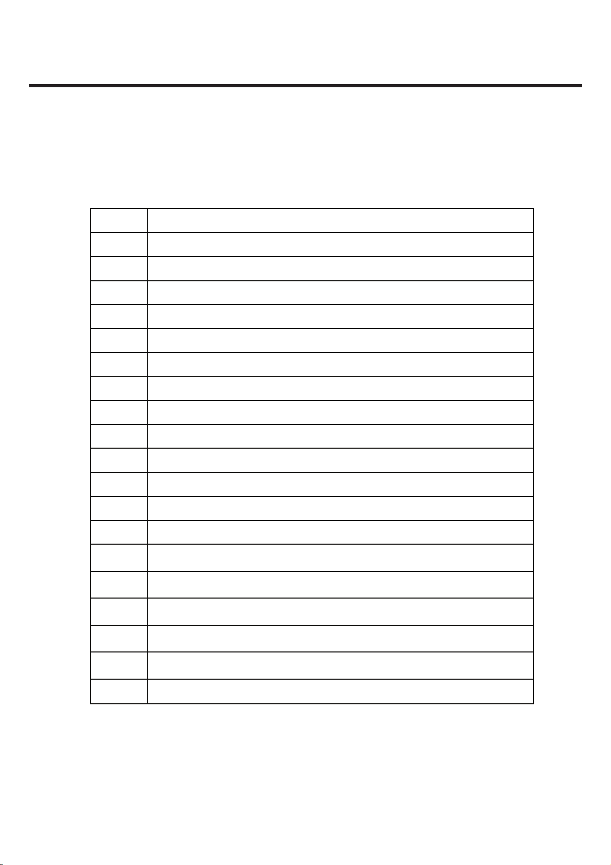
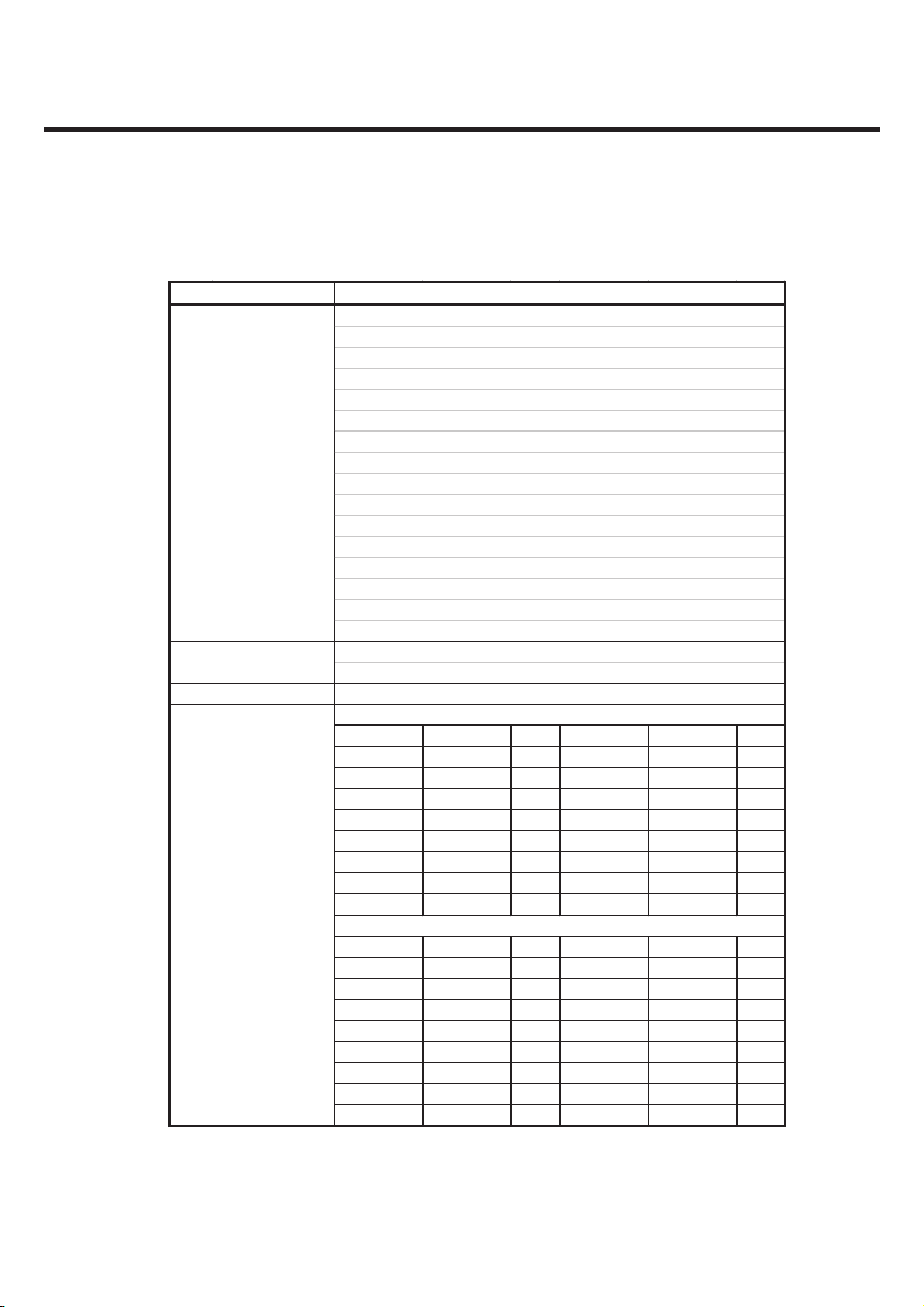
2.1 H/W Features
Item Feature Comment
Standard Battery Li-ion Polymer, 3.7V 800mAh
Stand by TIME Up to 200 hrs : Paging Period 5, RSSI 85dBm
Talk time Up to 200min : GSM Tx Level 7
Stand by time Up to 200 hours (Paging Period: 5, RSSI: -85 dBm)
Charging time Approx. 3 hours
2. SYSTEM SPECIFICATION
RX Sensitivity GSM, EGSM: -109dBm, DCS: -109dBm
TX output power
GPRS compatibility Class 12
EDGE compatibility Class 12
SIM card type 3V/1.8V Small
Display TFT 240 × 320 pixel 65K Color
KEYPAD
ANT Internal(GSM, Bluetooth)
EAR Phone Jack Yes
PC Synchronization Yes
Speech coding
Data and Fax Yes
Vibrator Yes
GSM, EGSM: 32.3dBm(Level 5),
DCS , PCS: 29.5dBm(Level 0)
0 ~ 9, #, *, Up/Down/Left/Right Navigation Key
Music Key, Clear Key, OK Key, PWR Key
Send Key, Soft Key(Left/Right)
Volume Key(Up/Down), Camera Key, Hold Key
EFR/FR/HR/AMR
3.5 Ø only
Loud Speaker Yes
Voice Recoding Yes
Microphone Yes
Copyright © 2009 LG Electronics. Inc. All right reserved.
Only for training and service purposes
- 9 -
LGE Internal Use Only
2. SYSTEM SPECIFICATION
Item Feature Comment
Speaker/Receiver Oval Type(1812), Speaker & Receiver Dual Mode
Travel Adapter Yes
MIDI SW MIDI (Mono SPK)
Camera 2M
Bluetooth / FM Radio Bluetooth version 2.1 / 76~108MHz supported
LGE Internal Use Only Copyright © 2009 LG Electronics. Inc. All right reserved.
- 10 -
Only for training and service purposes
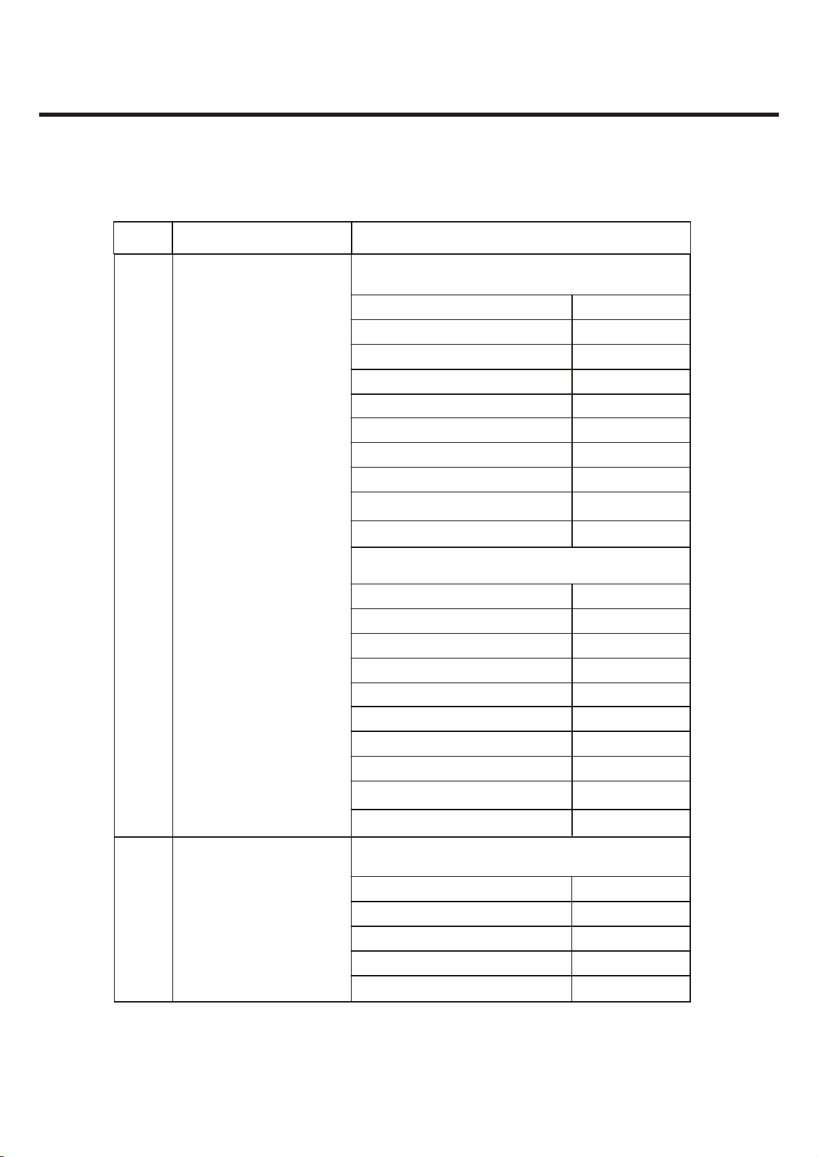
2.2 Technical Specification
2. SYSTEM SPECIFICATION
Item Description
1 Frequency Band
2 Phase Error
3 Frequency Error
4 Power Level
Specification
GSM850
TX: 824 + n ´ 0.2 MHz (n=1 ~ 124)
RX: TX + 45 MHz
GSM900
TX: 890 + n ´ 0.2 MHz (n=1 ~ 124)
890 + (n-1024) ´ 0.2 MHz (n=975 ~ 1023)
RX: TX + 45 MHz
DCS1800
TX: 1710 + ( n-511 ) ´ 0.2 MHz (n = 512 ~ 885)
RX: TX + 95 MHz
PCS1900
TX: 1850 + ( n-511 ) ´ 0.2 MHz
RX: 1930 + ( n-511 ) ´ 0.2 MHz (n = 512 ~ 810)
RMS < 5 degrees
Peak < 20 degrees
< 0.1ppm
GSM850/GSM900
Level Power Toler. Level Power Toler.
5 33 dBm ±2dB 13 17 dBm ±3dB
6 31 dBm ±3dB 14 15 dBm ±3dB
7 29 dBm ±3dB 15 13 dBm ±3dB
8 27 dBm ±3dB 16 11 dBm ±5dB
9 25 dBm ±3dB 17 9 dBm ±5dB
10 23 dBm ±3dB 18 7 dBm ±5dB
11 21 dBm ±3dB 19 5 dBm ±5dB
12 19 dBm ±3dB
DCS1800/PCS1900
Level Power Toler. Level Power Toler.
0 30 dBm ±2dB 8 14 dBm ±3dB
1 28 dBm ±3dB 9 12 dBm ±4dB
2 26 dBm ±3dB 10 10 dBm ±4dB
3 24 dBm ±3dB 11 8 dBm ±4dB
4 22 dBm ±3dB 12 6 dBm ±4dB
5 20 dBm ±3dB 13 4 dBm ±4dB
6 18 dBm ±3dB 14 2 dBm ±5dB
7 16 dBm ±3dB 15 0 dBm ±5dB
Copyright © 2009 LG Electronics. Inc. All right reserved.
Only for training and service purposes
- 11 -
LGE Internal Use Only
2. SYSTEM SPECIFICATION
Item Description Specification
GSM, EGSM
Offset from Carrier (kHz). Max. dBc
100 +0.5
200
250
400
600~ <1,200
1,200~ <1,800
1,800~ <3,000
3,000~ <6,000
5
Output RF Spectrum
(due to modulation)
DCS/PCS
Offset from Carrier (kHz). Max. dBc
6,000 -71
100 +0.5
200
250
400
600~ <1,200
1,200~ <1,800
-30
-33
-60
-60
-60
-63
-65
-30
-33
-60
-60
-60
1,800~ <3,000
3,000~ <6,000
6,000 -73
GSM, EGSM
Output RF Spectrum
6
LGE Internal Use Only Copyright © 2009 LG Electronics. Inc. All right reserved.
(due to switching
transient)
Offset from Carrier (kHz). Max. dBm
400
600
1,200 -21
1,800 -24
- 12 -
Only for training and service purposes
-65
-65
-19
-21
2. SYSTEM SPECIFICATION
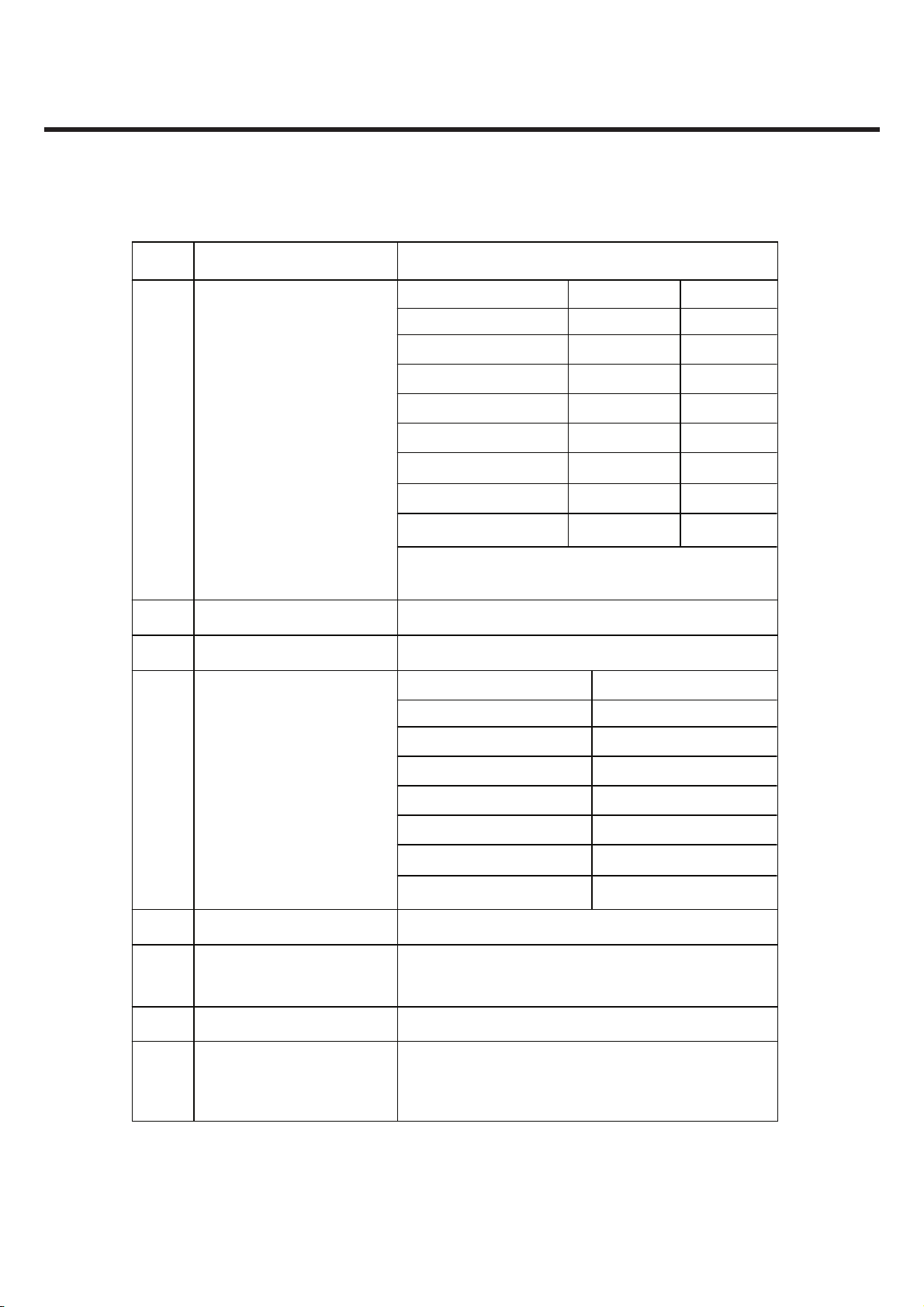
Item Description Specification
DCS/PCS
Offset from Carrier (kHz). Max. dBm
Output RF Spectrum
(due to switching
6
transient)
7 Spurious Emissions Conduction, Emission Status
GSM, EGSM
8 Bit Error Ratio
BER (Class II) < 2.439% @-104 dBm
DCS, PCS
BER (Class II) < 2.439% @-104 dBm
400
600
1,200 -24
1,800 -27
-22
-24
9 RX Level Report Accuracy ±3 dB
10 SLR 8±3 dB
Frequency (Hz) Max.(dB) Min.(dB)
11 Sending Response
12 RLR 2±3 dB
100 -
200 -
300
1,000 -6
2,000 -6
3,000 -6
3,400 -9
4,000
-12
0
0
0
4
4
4
0
-12
-
Copyright © 2009 LG Electronics. Inc. All right reserved.
Only for training and service purposes
- 13 -
LGE Internal Use Only
2. SYSTEM SPECIFICATION
Item Description Specification
Frequency (Hz) Max.(dB) Min.(dB)
100 -
-12
13 Receiving Response
* Mean that Adopt a straight line in between 300 Hz
and 1,000 Hz to be Max. level in the range.
14 STMR 13±5 dB
15 Stability Margin > 6 dB
dB to ARL (dB) Level Ratio (dB)
16 Distortion
200 -
300
500
1,000 -5
3,000 -5
3,400 -10
4,000
-35
-30
-20
-10
0
2
*
0
2
2
2
17.5
22.5
30.7
33.3
-7
-5
0
7
10
17 Side Tone Distortion Three stage distortion < 10%
18
19 32.768KHz tolerance ≤ 30 ppm
20 Ringer Volume
LGE Internal Use Only Copyright © 2009 LG Electronics. Inc. All right reserved.
System frequency
(13 MHz) tolerance
≤ 2.5 ppm
At least 65 dBspl under below conditions:
1. Ringer set as ringer.
2. Test distance set as 50 cm
- 14 -
Only for training and service purposes
33.7
31.7
25.5
2. SYSTEM SPECIFICATION
Item Description Specification
Fast Charge : Typ. 390 mA
21 Charge Current
Slow Charge : Typ. 80mA
Total Charging Time : < 3 hours
Bar Number Power
22 Antenna Display
23 Battery Indicator
24
Low Voltage Warning
( Blinking Bar)
7
7 -> 5
5 -> 4
4 -> 2
2 -> 1
1 -> 0 -106 ± 2
0 -> OFF
Battery Bar Number Voltage
3
3 -> 2
2 -> 1
1 -> 0
≤ 3.54 ± 0.05V (Call), 1/1-minute(Receiver)
≤ 3.4 ± 0.05V (Standby), 1/3-minute(Speaker)
-93 ~
-93 ± 2
-98 ± 2
-101 ± 2
-104 ± 2
~ -106
≥ 3.75± 0.05 V
3.75 ± 0.05 V
3.64 ± 0.05 V
3.54 ± 0.05 V
25
26
27 Battery Type
28 Travel Charger
Copyright © 2009 LG Electronics. Inc. All right reserved.
Only for training and service purposes
Forced shut down
Voltage
Sustain RTC
without battery
3.33 ± 0.05V
Over 50 hours
Li-Polymer Battery
Standard Voltage = 3.7 V
Battery full charge voltage = 4.2 V
Capacity: 800mAh
Switching-mode charger
Input: 100 ~ 350V, 50/60 Hz
Output: 5.6 V, 400 mA
- 15 -
LGE Internal Use Only
3. TECHNICAL BRIEF
3. TECHNICAL BRIEF
3.1 Main Processor(Digital Part : AD6725, U102)
Figure. 3-1-1 AD6725 FUNCTIONAL BLOCK DIAGRAM
The AD6725 is a tightly integrated single-package baseband processing solution offered by Analog Devices
as part of the AD20msp520 SoftFone® chipset family. The AD6725 incorporates all digital, analog, and power
management functions required in GSM, GPRS, EGPRS handsets with advanced multimedia and system
power management capabilities.
LGE Internal Use Only Copyright © 2009 LG Electronics. Inc. All right reserved.
- 16 -
Only for training and service purposes

3. TECHNICAL BRIEF
3.1.1 Features of AD6725
Complete Single-Chip Programmable Baseband Processor divided into several subsystems
MCU Control Processor Subsystem:
▪ 32-bit ARM926EJ-S® MCU Control Processor
▪ 208 MHz operation at 1.2V
▪ 2 dedicated caches, 16kB each, for instructions and data
▪ 4kB Instruction Tightly Coupled Memory (TCM)
▪ 2-Mbit On-chip System SRAM
▪ Ciphering coprocessor for GPRS supporting GEA1 and GEA2 encryption algorithms
▪ Kasumi cipher coprocessor for GEA3 encryption
▪ Dedicated multichannel DMA controller
DSP Subsystem:
▪ 16-bit fixed-point Blackfin® DSP Processor
▪ 208 MHz operation at 1.
▪ Memory:
→ L1 program space: 64 kB SRAM and 16 kB configurable as instruction cache
or SRAM
→ L1 data space: Two banks of 16K bytes, each with 8K bytes of dedicated SRAM
and an additional 8K bytes that can be configured as either cache or SRAM
→ L2 space: 64KB SRAM
▪ Ciphering coprocessor (GEA1 and GEA2)
▪ Kasumi cipher coprocessor for GEA3 encryption
▪ Dedicated multichannel DMA controller
Peripherals Subsystem:
▪ Shared on-chip peripherals and off-chip interfaces:
▪ Support for Burst-mode, Page-mode, and NAND Flash memory
▪ Support for SRAM, SDRAM, and PSRAM (cellular RAM)
▪ Full-Speed USB 2.0 Dual-Role Interface with OTG (On-The-Go) Host Mode or
traditional Peripheral-only mode
Copyright © 2009 LG Electronics. Inc. All right reserved.
Only for training and service purposes
- 17 -
LGE Internal Use Only

3. TECHNICAL BRIEF
▪ Serial Display Interface
▪ 8x8 Keypad Interface
▪ Thumbwheel Interface
▪ 4 Independent Programmable Backlights plus a Service Light
▪ 1.8V and 3.0V, 64 kbps SIM Interface
▪ Universal System Connector Interface
▪ Multimedia Card (MMC) Interface
▪ Secure Data (SD) Card Interface and SD I/O
▪ IrDA transceiver interfaces, including Fast IrDA (4 Mbps baud)
▪ 2 Configurable Generic Serial Ports (GSPs)
▪ 7 Configurable Enhanced Generic Serial Ports (eGSPs)
Applications Subsystem for Enhanced Multimedia:
▪ Dedicated 8/16/18-bit interface for parallel displays
▪ 8/10-bit Parallel Peripheral Interface (PPI) for camera sensor
▪ Image Signal Processing (ISP) module supporting resolutions up to 3.14 mega pixels.
▪ Flexible 2-D DMA controller
▪ Camera Flash synchronization strobe
▪ Hardware image scaling
▪ YCbCr/RGB color conversion
▪ JPEG decoder hardware Hardware
▪ JPEG compression
OTHER FEATURES
▪ Real-Time Clock (RTC) with Alarm
▪ Four General-Purpose Timers
▪ Compatible with Othello® radio subsystem
▪ Configurable interrupt controller architecture
▪ Programmable bus arbitration to optimize system performance
▪ Programmable Power Management and Clock Management
Slow Clocking Scheme for Low Idle Mode Current
Power Down modes
Dynamic Core Voltage Scaling
Active Leakage Current Management
▪ Independent I/O Voltage Domains
▪ On-chip support for EGPRS Data Services up to Class 12
▪ JTAG Interface for Test and In-Circuit Emulation of both the MCU and DSP
▪ Embedded Trace Macrocell for MCU Debug
▪ Advanced features for security Real-Time Clock (RTC) with Alarm
LGE Internal Use Only Copyright © 2009 LG Electronics. Inc. All right reserved.
- 18 -
Only for training and service purposes
3.2 Main Processor (Analog Part : AD6725, U102)
3. TECHNICAL BRIEF
AUDIO Subsystem
Radio Interface
Figure. 3-2-1 AD6725 FUNCTIONAL BLOCK DIAGRAM
The AD6725 is a complete mixed-signal baseband processor that combines all of the data converters and
power supply regulators required for a GSM 900 / GSM 850 / DCS 1800 / PCS 1900 mobile on a single device,
including HSCSD, GPRS and EGPRS.
Copyright © 2009 LG Electronics. Inc. All right reserved.
Only for training and service purposes
- 19 -
LGE Internal Use Only

3. TECHNICAL BRIEF
3.2.1 General Description
The AD6725 baseband transmit section supports the following mobile station GMSK
modulation power classes:
• GSM 900/850 power classes 4 and 5,
• DCS 1800 power classes 1 and 2, and
• PCS 1900 power classes 1 and 2.
The AD6725 baseband transmit section supports the following mobile station 8-PSK
modulation power classes:
• GSM 900/850 power classes E2 and E3,
• DCS 1800 power classes E2 and E3, and
• PCS 1900 power classes E2 and E3.
The AD6725 baseband receive section supports GMSK and 8-PSK applications.
The AD6725 auxiliary section provides a voltage reference, an automatic frequency control DAC, an auxiliary
ADC, and light controllers. The auxiliary ADC provides two channels for measuring temperature using discrete
external devices placed in critical locations. The AD6725 audio section provides 8 kHz and 16 kHz sampling
rates for voiceband data input and output and provides nine standard sample rates ranging from 8kHz to 48
kHz for personal audio output on two PCM Audio serial ports. The two Audio serial ports allow support for
concurrency. The AD6725 power management section provides voltage regulators for digital and analog
components, a battery charger, battery protection circuitry, and power supply activation logic. The AD6725
digital processor
interface provides serial ports for control data, baseband transmit and receive data, and two for audio data.
LGE Internal Use Only Copyright © 2009 LG Electronics. Inc. All right reserved.
- 20 -
Only for training and service purposes
3. TECHNICAL BRIEF
3.2.2 Power Block
CSPORT interface, power management control interface and the circuit that generates power up RESET
pulses(RESET1P8) for use by the DBB chip.
All regulators except the USB interface regulator are powered from the main battery.
The USB regulator is powered from USB VBUS.
And the user presses KEYON which puts the AD6725 power management system into ACTIVATION state
(see definitions below) and signals DBB software that it’s time to wake up and operate using the KEYOUT
signal.
Figure. 3-2-2 AD6725 POWER BLOCK DIAGRAM
Copyright © 2009 LG Electronics. Inc. All right reserved.
Only for training and service purposes
- 21 -
LGE Internal Use Only
3. TECHNICAL BRIEF
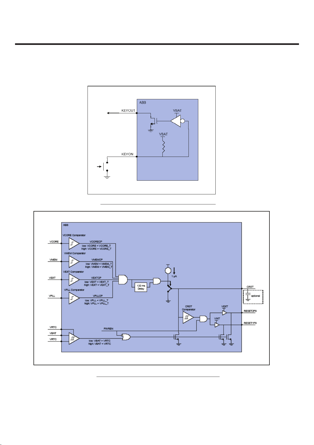
Figure. 3-2-3 AD6725 KEYON/KEYOUT BLOCK DIAGRAM
Figure. 3-2-4 AD6725 RESET GENERATION BLOCK DIAGRAM
LGE Internal Use Only Copyright © 2009 LG Electronics. Inc. All right reserved.
- 22 -
Only for training and service purposes

3. TECHNICAL BRIEF
Power On Reset Generator
The power-on reset signals (RESET1P8 and RESET2P8) are asserted based on the VCORE (if VAPPCFG = 0),
VMEM, VEXT, and VPLL regulators. RESET1P8 and RESET2P8 are low when reset is enabled and high when
reset is disabled.
When the outputs of all four regulators reach their corresponding threshold voltages, reset will be disabled
after a nominal reset period of 130ms.
The outputs of all four regulators must remain at or above their corresponding threshold voltages for the
duration of the reset period for reset to be disabled (pulled high).
The nominal 130ms reset period is restarted whenever all four regulators reach their threshold voltages.
The nominal reset period of 130ms can be extended by connecting an external capacitor to CRST. This
capacitor is charged using a small current when reset is enabled. Once the capacitor reaches the threshold,
reset is disabled.
Reset will be enabled immediately if any one of the four regulators falls below their corresponding
threshold voltages. In addition, reset will be enabled if VBAT falls below VRTC. The PWREN signal is the
logical AND of all the state controls that enable or disable many of the regulators on the chip. If the
regulators enabled by PWREN are
disabled by PMT state controls described below then PWREN must go low.
When PWREN goes low reset will be immediately enabled causing RESET1P8 and RESET2P8 to be pulled
low.
When reset is enabled, both RESET1P8 and RESET2P8 are actively pulled low.
CRST is also actively pulled low when reset is enabled.
VABB Regulator Enable/Disable Logic Operation
The VABB regulator powers many on-chip analog circuits on the ABB. The VCXOEN signal, the VABBEn bit
in the LDOControl1 Bit Positions ( Addr 0x35) register, and the AFCDACMode and AFCDACOn bits in the
AuxControl1 Bit Positions ( Addr 0x13) register all particpate in controlling the VABB enable/disable.
When the ABB power management system transitions from Off state, DDLO state, UVLO state, or Thermal
Shutdown State to Power Key Activation, Charger Activation, USB Charger Activation, or Active State VABB
will be enabled. During these state transitions ABBEn = 0 and AFCDACMode = 0, VRF is enabled.
Once the ABB power management system is in Power Key Activation, Charger Activation, USB Charger
Activation, Active-Standby or Active State the VABB regulator enable/disable is controlled by the
information written to the VABBEn and AFCDACMode register bits by system software.
Copyright © 2009 LG Electronics. Inc. All right reserved.
Only for training and service purposes
- 23 -
LGE Internal Use Only

3. TECHNICAL BRIEF
Digital Baseband Core (VCORE)
The Digital Baseband Core regulator supplies the digital baseband processor (DBB) core.
The voltage on VCORE is selectable using the VCOREControl register.
The VCOREActive code selects the voltage on VCORE in high power mode and the VCOREStandby code
selects the voltage on VCORE in low-power mode.
DBB Interface (VINT)
The DBB interface regulator supplies the DBB/ABB digital interfaces. The output voltage of the VINT regulator
is nominal 1.8V.
Memory (VMEM)
The VMEM regulator supplies the external memory(s) and the interface to the external memory on the digital
baseband processor. The output voltage of the Memory Interface regulator can be selected as 1.8V nominal
or 2.8V nominal using the VMEMSEL terminal.
External Interface (VEXT)
The External Interface regulator supplies the Radio digital interface and the high voltage (>1.8V) interface
between the digital baseband processor and various peripherals, such as the LED indicators and the LCD
display.
SIM Interface (VSIM)
AD6725 is designed to support 3.0 V and 1.8 V SIMs exclusively (i.e. no 5 V SIMs).
The SIM Interface regulator supplies the SIM interface circuitry on the digital processor and the SIM card. By
default the SIM Interface regulator output is 2.85 V, which can be decreased to 1.8 V if a 1.8 V SIM is detected.
Real-Time Clock (VRTC)
The Real-Time Clock regulator supplies the Real-Time Clock module. The Real-Time Clock regulator is
optimized for low ground current.
LGE Internal Use Only Copyright © 2009 LG Electronics. Inc. All right reserved.
- 24 -
Only for training and service purposes

3. TECHNICAL BRIEF
Baseband Analog (VABB)
The Baseband Analog regulator supplies the analog portions of the AD6725. Operation of the VABB
regulator is controlled by the VABBEn bit in the LDOControl1 register.
If VABBEn = 0, the VABB regultor will be disabled unless the AFCDAC is enabled or VCXOEN = 1. If VABBEn
= 1 (the default state) VABB is enabled along with VCORE, VMEM, and VEXT. The Baseband Analog
regulator is optimized for high ripple rejection and low noise. The output of the Baseband Analog
regulator should not be used as a supply for any external components.
Microphone (VMIC)
The Microphone regulator supplies the microphone interface circuitry. The Microphone regulator is
optimized for extremely high ripple rejection up to 217 Hz and low noise.
VRF (VRF)
The VCXO regulator supplies the voltage controlled crystal oscillator (VCXO). The VCXO regulator is
optimized for high ripple rejection and low noise.
USB Interface (VUSB)
The VUSB regulator supplies the USB transceiver located in the DBB. Digital Baseband PLL (VPLL) The
VPLL regulator supplies the phase locked loop on the digital baseband (DBB).
General Purpose Regulator (VGP)
The General Purpose regulator is intended primarily to serve as a supply rail for camera modules. Its
voltage is programmable by setting VGPSel[3:0] in theLDOControl2 Register. VGP is enabled by setting
the VGPEn bit in LDOControl1 to 1.
Applications Regulator (VAPP)
The VAPP regulator is an adjustable regulator that uses an off chip pass device. It has two modes of
operation selected by the state of the VAPPCFG terminal. If VAPPCFG is pulled low the VAPP regulator
functions as a programmable voltage applications supply.
In this mode, VAPP is enabled or disabled using the VAPPEn bit of LDOControl1.
Copyright © 2009 LG Electronics. Inc. All right reserved.
Only for training and service purposes
- 25 -
LGE Internal Use Only
3. TECHNICAL BRIEF
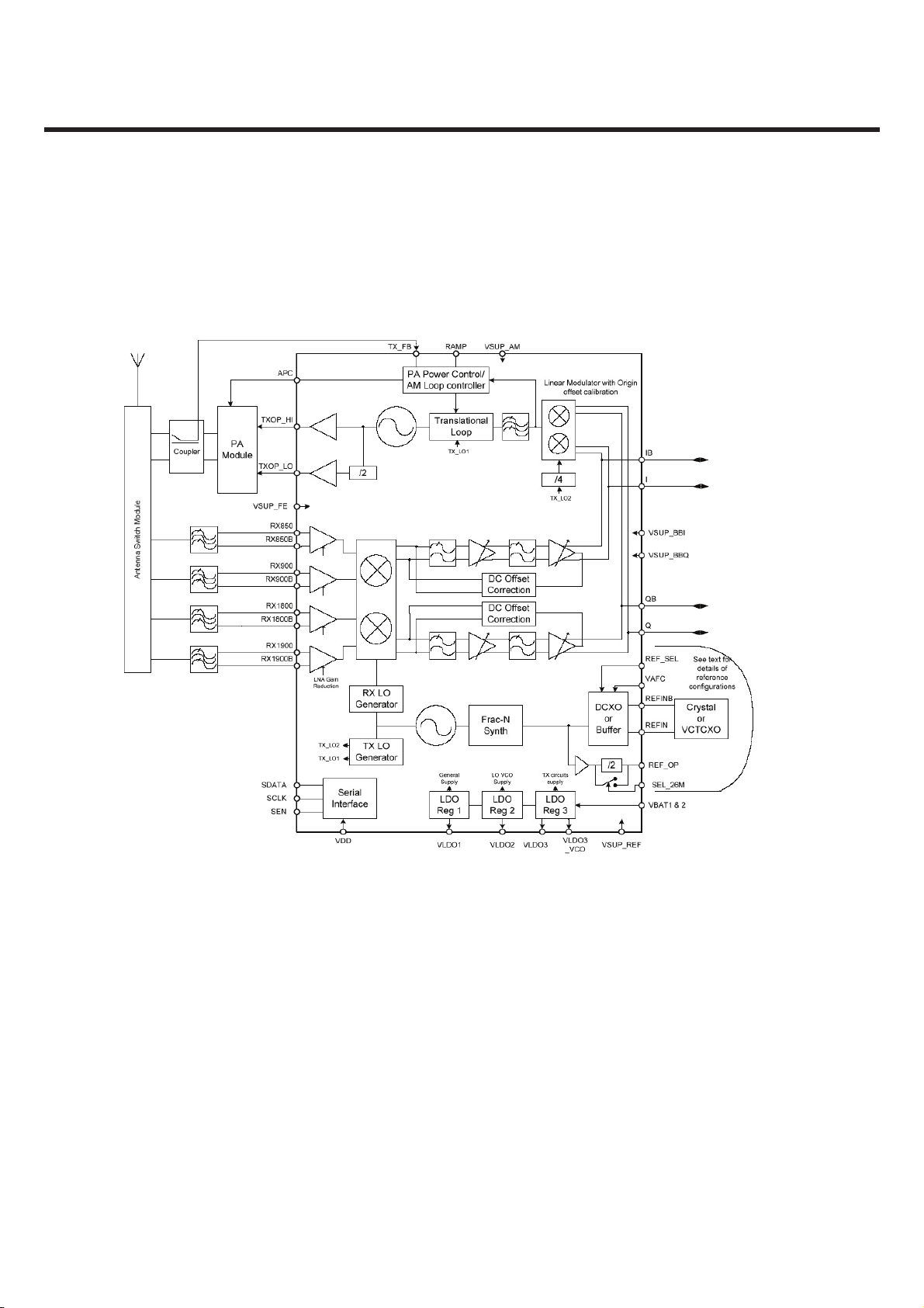
3.3 RF Transceiver (AD6546)
3.3.1 Internal Block Diagram
Figure 3-3-1 AD6546 FUNCTIONAL BLOCK DIAGRAM
3.3.2 General Description
The AD6546 is a fully integrated Quad band GSM Transceiver with an advanced modulator design that fully
supports 8-PSK EDGE modulation format.
The AD6546 contains a translation loop modulator for directly modulating baseband signals onto an
integrated Tx VCO. The translation loop modulator and Tx VCO are extremely low noise removing the need
for external TX filtering.
LGE Internal Use Only Copyright © 2009 LG Electronics. Inc. All right reserved.
- 26 -
Only for training and service purposes
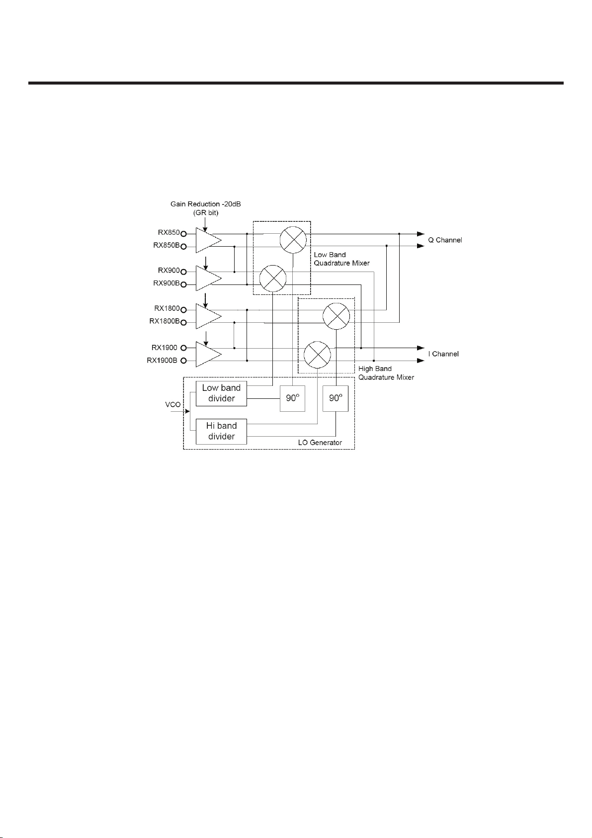
3.3.2.1 Receiver
3. TECHNICAL BRIEF
Figure 3-3-2 AD6546 RECEIVER
Low Noise Amplifiers
The LNAs have differential inputs which help minimize the effect of unwanted interferers. The
voltage gain of the LNAs is typically 24 dB. Each LNA can be switch to a low gain mode when
receiving large input signals as part of the AGC system.
Down-Converting Mixers
Two quadrature mixers are used to mix down the signals from the LNAs, one for the high bands (1800
and 1900 MHz) and one for the low bands (850 and 900 MHz). The outputs of the mixers are
connected to the baseband section through an integrated
single pole filter with nominal cut-off frequency of 800kHz.
Copyright © 2009 LG Electronics. Inc. All right reserved.
Only for training and service purposes
- 27 -
LGE Internal Use Only
3. TECHNICAL BRIEF
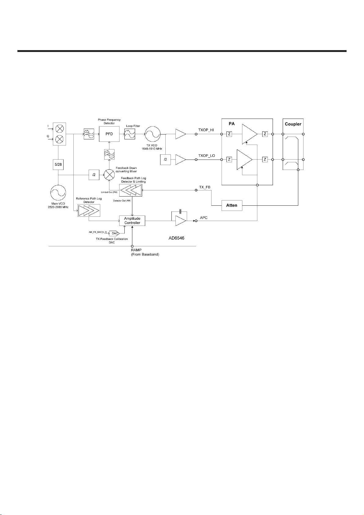
3.3.2.2 Transmitter
Figure 3-3-3 AD6546 TRANSMITTER
Transmitter Overview
The highly integrated transmit section of the AD6546 radio has been designed to fully support 8 PSK
modulation for EDGE applications, and GMSK modulation for GSM. A translational loop is used for
phase modulation, and for 8 PSK additional envelope (AM) circuits are enabled to implement a Polar
modulator.
Quadrature Modulator
The Quadrature modulator takes the baseband I/Q signals and converts this onto a complex
modulated signal (containing both amplitude and phase information) at the TX IF frequency. After
bandpass filtering the TX IF signal is used as the reference
input to the Phase Frequency Detector (PFD) for the transmit PLL, and in EDGE mode also provides
the input to the Reference Path Log Detector circuit for AM restoration.
LGE Internal Use Only Copyright © 2009 LG Electronics. Inc. All right reserved.
- 28 -
Only for training and service purposes
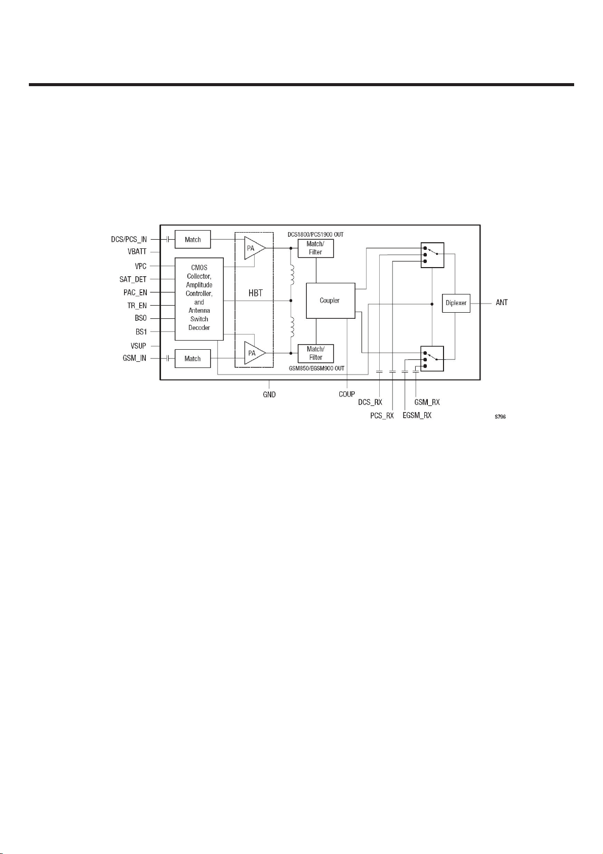
3.4 Power Amplifier Module (SKY77523)
3.4.1 Internal Block Diagram
3. TECHNICAL BRIEF
Figure 3-4-1 SKY77523 FUNCTIONAL BLOCK DIAGRAM
3.4.2 General Description
The SKY77523 provides a complete transmit Voltage-Controlled Oscillator (VCO)-to-antenna and
antenna-to-receive Surface Acoustic Wave (SAW) filter solution.
The module consists of a single GSM850/EGSM900 and DCS1800/PCS1900 PA block, a PA Control (PAC)
block, impedance-matching circuitry for 50 Ω inputs and outputs, transmit harmonic filtering, an
integrated coupler, high-linearity and low insertion-loss PHEMT RF switches, and a diplexer. A custom
CMOS integrated circuit provides the internal PAC function, interface circuitry, and decoder circuitry to
control the RF switches.
Copyright © 2009 LG Electronics. Inc. All right reserved.
Only for training and service purposes
- 29 -
LGE Internal Use Only
3. TECHNICAL BRIEF
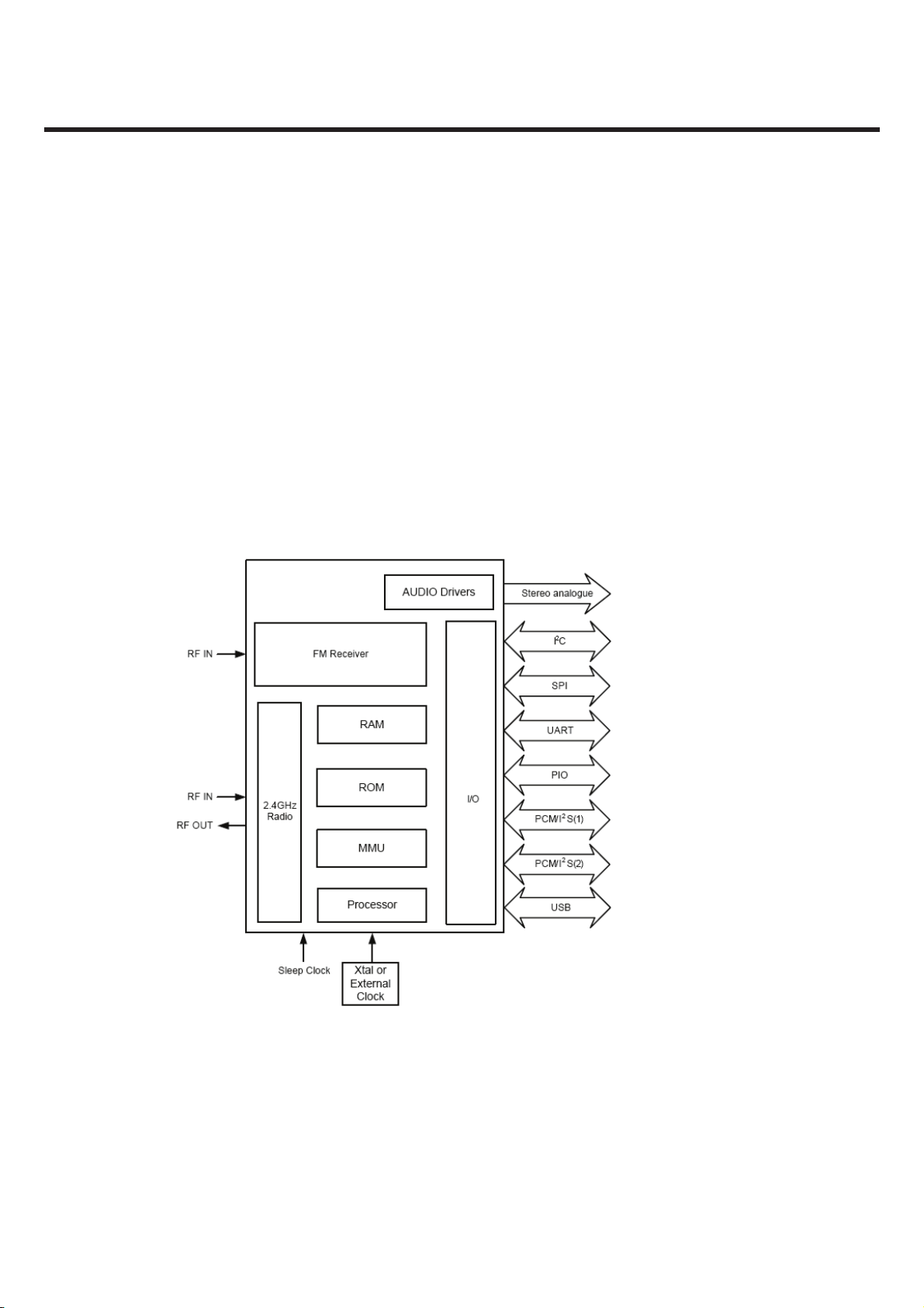
3.5 BT Module with integrated FM tuner
3.5.1 General Description
The BlueCore 5-FM BGA is a single-chip radio and baseband IC for Bluetooth 2.4GHz systems including
enhanced data rates (EDR) to 3Mbits/s.
It includes anintegrated FM receiver with stereo audio output stage and an RDS demodulator. With the
on-chip CSR Bluetooth software stack, it provides a fully compliant Bluetooth system to v2.1 +EDR of
the specification for data and voice communications.
3.5.2 Total internal Block Diagram
Figure 3-5-1 Total Internal Block Diagram
LGE Internal Use Only Copyright © 2009 LG Electronics. Inc. All right reserved.
- 30 -
Only for training and service purposes
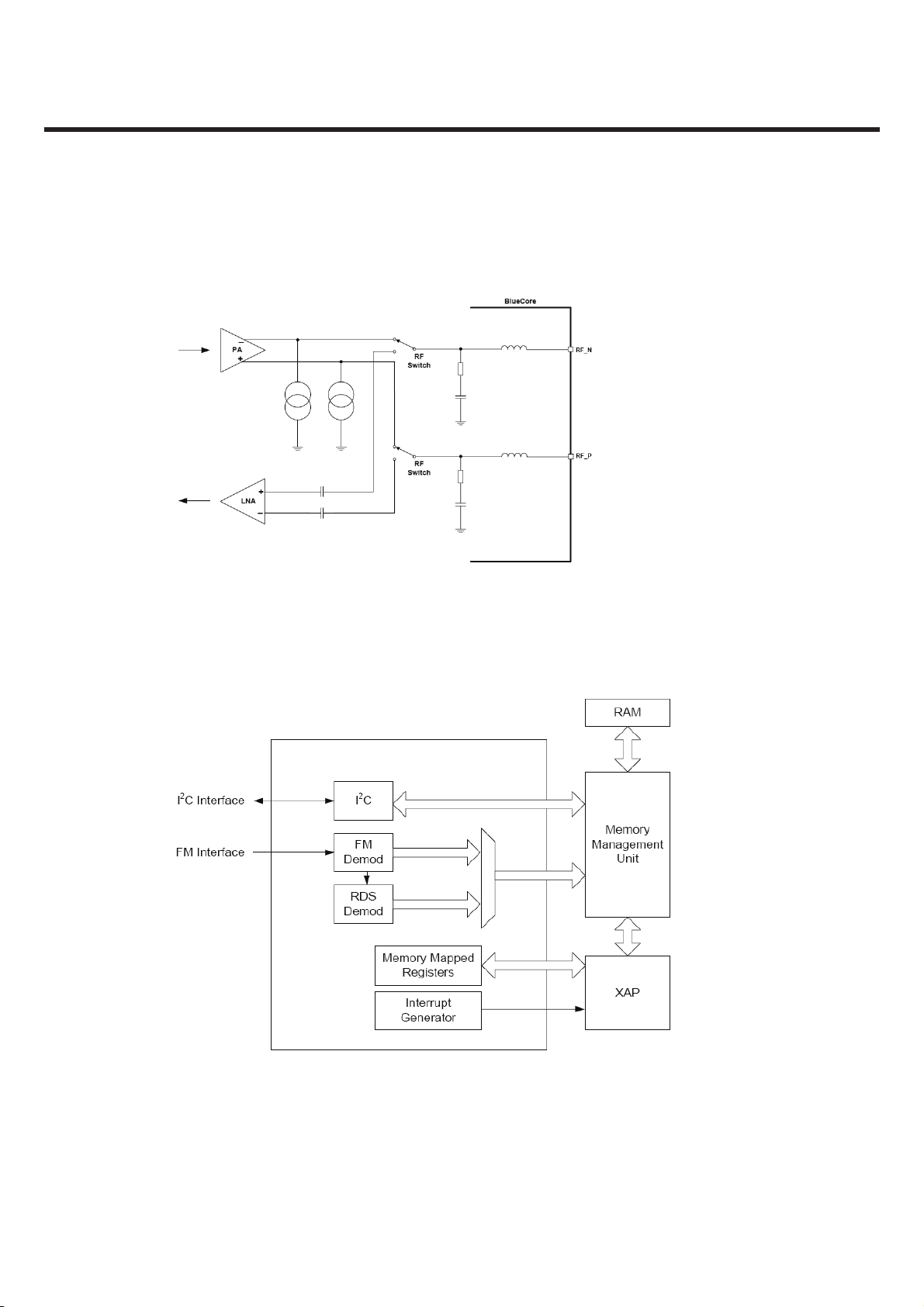
3.5.3 BT radio internal Block Diagram
3. TECHNICAL BRIEF
Figure 3-5-2 BT radio internal Block Diagram
3.5.4 FM radio internal Block Diagram
Figure 3-5-3 FM Radio internal Block Diagram
Copyright © 2009 LG Electronics. Inc. All right reserved.
Only for training and service purposes
- 31 -
LGE Internal Use Only
 Loading...