

LG GD580 Service Manual
Service Manual Model : GD580
Internal Use Only
Service Manual
GD580
Date: November, 2009 / Issue 1.0

Table Of Contents
1. Introduction ...................................................5
1.1 Purpose ......................................................................5
1.2 Regulatory Information .................................................5
1.3 Abbreviation ................................................................7
2. performance ...................................................9
2.1 System Overview .........................................................9
2.2. Usable environment ..................................................10
2.3 Radio Performance ....................................................11
2.4 Current Consumption .................................................19
2.5 RSSI .........................................................................19
2.6 Battery Bar ................................................................19
2.7 Sound Pressure Level ................................................20
2.8 Charging ...................................................................21
3. Technical brief .............................................22
3.1 Digital Baseband(DBB) & Multimedia Processor ...........22
4.10 Charger Trouble Shooting .......................................113
4.11 Bluetooth Trouble ...................................................116
4.12 RF Component ......................................................119
4.13 Procedure to check ...............................................120
4.14 Checking Common Power Source Block ..................121
4.15 Checking VCXO Block ............................................128
4.16 Checking Front End Module Block ..........................132
4.17 Checking Front End Module Block input logic ..........133
4.18 Checking WCDMA Block ........................................142
4.19 Checking GSM Block .............................................155
5. Download ................................................... 167
5.1 Requirements ..........................................................167
5.2. GD580 Download ...................................................168
5.3 Trouble Shooting ......................................................175
6. Block diagram ............................................ 170
3.2 GAM Hardware Subsystem .........................................44
3.3. Audio Part ................................................................53
3.4 GPADC(General Purpose ADC) and AUTOADC2 ............61
3.5 Charger control .........................................................62
3.6. Voltage Regulation ....................................................68
3. 7 RF Technical Description ...........................................69
4. Trouble Shooting .......................................... 79
4.1 Power ON Trouble ......................................................79
4.2 USB Trouble ..............................................................80
4.3 SIM Detect Trouble ....................................................81
4.4 MicroSD card Trouble ................................................82
4.5 Key and Touch Screen Trouble ....................................83
4.6 Camera Trouble .........................................................85
4.7 Main LCD Trouble ......................................................92
4.8 Keypad Backlight Trouble ...........................................96
7. Circuit Diagram .......................................... 181
8. BGA Pin Map .............................................. 191
9. PCB Layout .................................................197
10. Calibration ................................................ 205
10.1 General Description ...............................................205
10.2 XCALMON Environment .........................................205
10.3 Calibration Environment .........................................206
10.4 Program Operation ................................................207
11. Exploded view & Replacement part list . 213
11.1 Exploded view .......................................................213
11.2 Replacement Parts ................................................215
12.3 Accessory .............................................................237
4.9 Audio Trouble Shooting ..............................................99
Copyright © 2009 LG Electronics. Inc. All right reserved.
Only for training and service purposes
- 3 -
LGE Internal Use Only

LGE Internal Use Only Copyright © 2009 LG Electronics. Inc. All right reserved.
- 4 -
Only for training and service purposes

1. Introduction
1. INTRODUCTION
1. Introduction
1.1.Purpose
This manual provides the information necessary to repair, calibration, description and download the
features of the KM555E.
GD580.
1.2.Regulatory Information
A. Security
Toll fraud, the unauthorized use of telecommunications system by an unauthorized part (for example,
persons other than your company’s employees, agents, subcontractors, or person working on your
company’s behalf) can result in substantial additional charges for your telecommunications services.
System users are responsible for the security of own system.
There might be risks of toll fraud associated with your telecommunications system. System users are
responsible for programming and configuring the equipment to prevent unauthorized use. LGE does
not warrant that this product is immune from the above case but will prevent unauthorized use of
common carrier telecommunication service of facilities accessed through or connected to it. LGE will
not be responsible for any charges that result from such unauthorized use.
B. Incidence of Harm
If a telephone company determines that the equipment provided to customer is faulty and possibly
causing harm or interruption in service to the telephone network, it should disconnect telephone
service until repair can be done. A telephone company may temporarily disconnect service as long as
repair is not done.
C. Changes in Service
A local telephone company may make changes in its communications facilities or procedure. If these
changes could reasonably be expected to affect the use of the KM555E or compatibility with the net
work, the telephone company is required to give advanced written notice to the user, allowing the user
to take appropriate steps to maintain telephone service.
GD580
D. Maintenance Limitations
Maintenance limitations on the KM555E must be performed only by the LGE or its authorized agent.
The user may not make any changes and/or repairs expect as specifically noted in this manual.
Therefore, note that unauthorized alternations or repair may affect the regulatory status of the system
and may void any remaining warranty.
GD580
Copyright © 2009 LG Electronics. Inc. All right reserved.
Only for training and service purposes
- 5 -
LGE Internal Use Only

1. Introduction
KM555E service manual
E. Notice of Radiated Emissions
This model complies with rules regarding radiation and radio frequency emission as defined by local
regulatory agencies. In accordance with these agencies, you may be required to provide information
such as the following to the end user.
F. Pictures
The pictures in this manual are for illustrative purposes only; your actual hardware may look slightly
different.
G. Interference and Attenuation
KM555E may interfere with sensitive laboratory equipment, medical equipment, etc. Interference from
GD580
unsuppressed engines or electric motors may cause problems.
H. Electrostatic Sensitive Devices
ATTENTION
Boards, which contain Electrostatic Sensitive Device (ESD), are indicated by the sign. Following
information is ESD handling:
• Service personnel should ground themselves by using a wrist strap when exchange system boards.
• When repairs are made to a system board, they should spread the floor with anti-static mat which is
also grounded.
• Use a suitable, grounded soldering iron.
• Keep sensitive parts in these protective packages until these are used.
• When returning system boards or parts like EEPROM to the factory, use the protective package as
described.
LGE Internal Use Only Copyright © 2009 LG Electronics. Inc. All right reserved.
- 6 -
Only for training and service purposes

1. Introduction
KM555E service manual
1.3 Abbreviation
For the purposes of this manual, following abbreviations apply:
1. Introduction
APC Automatic Power Control
BB Baseband
BER Bit Error Ratio
CC-CV Constant Current – Constant Voltage
CLA Cigar Lighter Adapter
DAC Digital to Analog Converter
DCS Digital Communication System
dBm dB relative to 1 milli-watt
DSP Digital Signal Processing
EEPROM Electrical Erasable Programmable Read-Only Memory
EGPRS Enhanced General Packet Radio Service
EL Electroluminescence
ESD Electrostatic Discharge
FPCB Flexible Printed Circuit Board
GMSK Gaussian Minimum Shift Keying
GPIB General Purpose Interface Bus
GPRS General Packet Radio Service
GSM Global System for Mobile Communications
IPUI International Portable User Identity
IF Intermediate Frequency
LCD Liquid Crystal Display
LDO Low Drop Output
LED Light Emitting Diode
LGE LG Electronics
OPLL Offset Phase Locked Loop
PAM Power Amplifier Module
PCB Printed Circuit Board
PGA Programmable Gain Amplifier
PLL Phase Locked Loop
Copyright © 2009 LG Electronics. Inc. All right reserved.
Only for training and service purposes
- 7 -
LGE Internal Use Only

1. Introduction
KM555E service manual
PSTN Public Switched Telephone Network
RF Radio Frequency
RLR Receiving Loudness Rating
RMS Root Mean Square
RTC Real Time Clock
SAW Surface Acoustic Wave
SIM Subscriber Identity Module
SLR Sending Loudness Rating
SRAM Static Random Access Memory
STMR Side Tone Masking Rating
TA Travel Adapter
TDD Time Division Duplex
TDMA Time Division Multiple Access
UART Universal Asynchronous Receiver/Transmitter
VCO Voltage Controlled Oscillator
VCTCXO
WAP
8PSK 8 Phase Shift Keying
Voltage Control Temperature Compensated Crystal
Oscillator
Wireless Application Protocol
LGE Internal Use Only Copyright © 2009 LG Electronics. Inc. All right reserved.
- 8 -
Only for training and service purposes
2. Performance
2.1 System Overview
Item Specifications
2. Performance
Band
Type
Dimension
Weight
Power
Talk Time
Stand-by Time
Antenna
LCD(Main)
Back Light
Back Light color
Vibrator
Speaker
GSM Triple Band(900/1800/1900), UMTS, Bluetooth
Folder type
108.3 x 51.5 x 13.4mm
103.5g [87.0g With out Battery]
800mAh Li-Ion
Over 170 Min (WCDMA, Tx=12dBm, @ Voice)
Over 180 Min (GSM, Tx=Max, @ Voice)
Over 250 hours (WCDMA, DRX=7
GSM, Paging period=5)
Intenna Type
240x400Pixel
Yes
White
Yes (Coin Type)
Yes
MIC
Receiver
Earphone Jack
SIM Socket
Volume Key
Voice Key
I/O Connect
Copyright © 2009 LG Electronics. Inc. All right reserved.
Only for training and service purposes
Yes ( SMT Type) /2EA
1 for speaker phone/1 for Voice call
Yes
Yes
Yes(SIM Block Type) : 3.0V & 1.8V
Push Type(+,-)
Push Type
18 Pin
- 9 -
LGE Internal Use Only
2. Performance
2.2 Usable environment
1) Environment
Item Spec. Unit
Voltage 3.7 (Typ), 3.4 (Min), (Shut Down: 3.2) V
Operating Temp. -20 ~ + 60 °C
Storage Temp. -30 ~ + 85 °C
Humidity max. 85 %
2) Environment (Accessory)
Item Spec. Min Typ. Max Unit
Power Available power 100 220 240 Vac
* CLA : 12~24V (DC)
LGE Internal Use Only Copyright © 2009 LG Electronics. Inc. All right reserved.
- 10 -
Only for training and service purposes
2.3 Radio Performance
1) Transmitter – GSM Mode
2. Performance
NO
1
ITEM
Conducted
Spurious
Emission
MS
allocated
Channel
Idle Mode
MS
allocated
Channel
GSM900 DCS1800 PCS1900
9k ~ 1GHz -36dBm
9k ~ 1GHz -36dBm
1G ~ 1710MHz -30dBm
1710M ~
1G ~ 12.75GHz -30dBm
9k ~ 880MHz -57dBm 9k ~ 880MHz -57dBm 9k ~ 880MHz -57dBm
880M ~ 915MHz -59dBm 880M ~ 915MHz -59dBm 880M ~ 915MHz -57dBm
915M ~ 1000Mz -57dBm 915M ~ 1000MHz -57dBm 915M ~ 1000MHz -57dBm
1G ~ 1.71GHz -47dBm 1G ~ 1.71GHz -47dBm 1G ~ 1.85GHz -47dBm
1.71G ~
1.785GHz
1.785G ~
12.75GHz
30M ~ 1GHz -36dBm
1G ~ 4GHz -30dBm
-53dBm
-47dBm
1785MHz
1785M ~
12.75GHz
1.71G ~
1.785GHz
1.785G ~
12.75GHz
30M ~ 1GHz -36dBm
1G ~ 1710MHz -30dBm
1710M ~
1785MHz
1785M ~ 4GHz -30dBm
-36dBm
-30dBm
-53dBm 1.85G ~ 1.91GHz -53dBm
-47dBm
-36dBm
9k ~ 1GHz -36dBm
1G ~ 12.75GHz -30dBm
1.91G ~
12.75GHz
30M ~ 1GHz -36dBm
1G ~ 4GHz -30dBm
-47dBm
Radiated
Spurious
Emission
Idle Mode
2 Frequency Error
3 Phase Error
Copyright © 2009 LG Electronics. Inc. All right reserved.
Only for training and service purposes
30M ~ 880MHz -57dBm 30M ~ 880MHz -57dBm 30M ~ 880MHz -57dBm
880M ~ 915MHz -59dBm 880M ~ 915MHz -59dBm 880M ~ 915MHz -59dBm
915M ~
1000MHz
1G ~ 1.71GHz -47dBm 1G ~ 1.71GHz -47dBm 1G ~ 1.85GHz -47dBm
1.71G ~
1.785GHz
1.785G~ 4GHz -47dBm 1.785G~ 4GHz -47dBm 1.91G~ 4GHz -47dBm
0.1ppm
5(RMS)
20(PEAK)
-57dBm 915M ~ 1000MHz -57dBm 915M ~ 1000MHz -57dBm
-53dBm
- 11 -
1.71G ~
1.785GHz
0.1ppm
5(RMS)
20(PEAK)
-53dBm 1.85G ~ 1.91GHz -53dBm
0.1ppm
5(RMS)
20
(PEAK)
LGE Internal Use Only
2. Performance
NO ITEM GSM900 DCS1800 PCS1900
Frequency Error
Under
Multipath and RA250: 300Hz RA130: 400Hz RA130: 420Hz
4
5
7
8
9 Burst timing Mask IN Mask IN Mask IN
*. Output RF Spectrum (Modulation) Absolute Specification <3GPP TS 05.05, subclause 4.2.1>
interference HT100: 180Hz HT100: 350Hz HT100: 370Hz
Condition TU50: 160Hz TU50: 260Hz TU50: 280Hz
Due to
modulati
on
Output RF
Spectrum
Due to
Switchin
g
transient
Intermodulation
attenuation
Transmitter Output
Power
3dB below reference
sensitivity
TU3: 230Hz TU1.5: 320Hz TU1.5: 330Hz
0 ~ 100kHz +0.5dB 0 ~ 100kHz +0.5dB 0 ~ 100kHz +0.5dB
200kHz -30dB 200kHz -30dB 200kHz -30dB
250kHz -33dB 250kHz -33dB 250kHz -33dB
400kHz -60dB 400kHz -60dB 400kHz -60dB
600 ~ 1800kHz -60dB 600 ~ 1800kHz -60dB 600 ~ 1200kHz -60dB
1800 ~ 3000kHz -63dB 1800 ~ 6000kHz -65dB 1200 ~ 1800kHz -60dB
3000 ~ 6000kHz -65dB >= 6000kHz -73dB 1800 ~ 6000kHz -65dB
>=6000kHz -71dB >= 6000kHz -73dB
400kHz -19dB 400kHz -22dB 400kHz -22dB
600kHz -21dB 600kHz -24dB 600kHz -24dB
1200kHz -21dB 1200kHz -24dB 1200kHz -24dB
1800kHz -24dB 1800kHz -27dB 1800kHz -27dB
-
Power
control
Level (dBm) Level (dBm) (dB) Level (dBm) (dB)
Power
53330 3030 303
63131 2831 28
72932 2632 263
82733 2433 243
92534 2234 223
10 23
11 21
12 19
13 17
14 15
15 13
16 11
17 9
18 7
19 5
3dB below reference
sensitivity
Frequency offset 800kHz
Intermodulation product
should be Less than 50dB
below the level of Wanted
signal
Power
control
35 2035 203
36 1836 183
37 1637 163
38 1438 143
39 1249 124
310 10410 104
511 8411 84
512 6412 64
513 4413 44
514 2514 25
Power
15 0
TolerancePower
3dB below reference
sensitivity
control
515 05
-
Power
Toleran
ce
3
Frequency offset from the carrier
< 600 kHz 36 dBm 36 dBm
³ 600 kHz, < 1 800 kHz 51 dBm 56 dBm
³1800kHz 46 dBm 51 dBm
LGE Internal Use Only Copyright © 2009 LG Electronics. Inc. All right reserved.
GSM 400 & GSM 900
& GSM 850
- 12 -
DCS 1 800 &PCS 1 900
Only for training and service purposes
2) Transmitter – WCDMA Mode
2. Performance
No
Maximum Output Power Class3: +24dBm(+1/-3dB)
1
2
Open Loop Power control
3
Item Specification
Frequency Error ±0.1ppm
in uplink
±9dB@normal, ±12dB@extreme
Adjust output (TPC command)
cmd 1dB 2dB 3dB
Inner Loop Power control
4
in uplink
+1 +0.5/1.5 +1/3 +1.5/4.5
0 -0.5/+0.5 -0.5/+0.5 -0.5/+0.5
-1 -0.5/-1.5 -1/-3 -1.5/-4.5
group(10equal command group)
+1 +8/+12 +16/+24
Minimum Output Power < -50dBm(3.84MHz)
5
Out-of-synchronization
6
handling of output power
Qin/Qout:DPCCH quality levels
Toff@DPCCH/lor:-22->-28dB
Ton@DPCCH/lor:-24->-18dB
7
8
9
10
11
Transmit OFF Power -56dBm(3.84M)
Transmit ON/OFF Time
Mask
Change of TFC
Power setting in uplink
compressed
Occupied
Bandwidth(OBW)
1213 Spectrum emission Mask
Adjacent Channel
Leakage Ratio(ACLR)
±25us
PRACH, CPCH, uplink compres sed mode
±25us
power varies according to the data rate
DTX: DPCH off
(minimize interference between UE)
±3dB(after 14slots transmission gap)
< 5MHz(99%)
-35-15*(f-2.5)dBc @f=2.5~3.5MHz, 30k
-35-1*(f-3. 5)dBc@f=3.5~7.5MHz, 1M
-39-10*(f-7.5)dBc @f=7.5~8.5MHz, 1M
-49 dBc@f=8. 5~12. 5MHz, 1M
-33dBc@5MHz, ACP>-50dBm
-43dBc@10MHz, ACP>-50dBm
Copyright © 2009 LG Electronics. Inc. All right reserved.
Only for training and service purposes
- 13 -
LGE Internal Use Only
2. Performance
14
Spurious Emissions
*: additional requirement
-36dBm@f=9~150KHz, 1k BW
-36dBm@f=150KHz~30MHz, 10k
-36dBm@f=30~1000MHz, 100k
-30dBm@f=1~12.75GHz, 1M
-41dBm*@1893.5~1919.6MHz, 300k
-67dBm*@925~935MHz, 100k
-79dBm*@935~960MHz, 100k
-71dBm*@1805~1880MHz, 100k
Trans mit Intermodulation
15
16
17
Error Vector
Magnitude(EVM)
Transmit OFF Power
-31dBc@5MHz, Interferer -40dBc
-41dBc@10MHz, Interferer -40dBc
17.5% (>-20dBm)
(@12.2k, 1DPDCH+1DPCCH)
-15dB@SF=4, 768kbps,
multi-code transmission
LGE Internal Use Only Copyright © 2009 LG Electronics. Inc. All right reserved.
- 14 -
Only for training and service purposes
3) Receiver - GSM Mode
2. Performance
NO
Sensitivity (TCH/FS Class
1
Co-Channel Rejection
2
(TCH/FS Class II,RBER,
Adjacent
Channel
3
Rejection
(Speech
Channel)
4 Intermodulation Rejection
5
Bloc king Response
(TCH/FS Clas s II, RBER)
Item GSM850/GSM900 DCS1800/PCS1900
II)
TUhigh/ F H)
200kHz C/Ia1= -12dB C/Ia1= -12dB
400kHz
-105dBm -105dBm
C/Ic= 7dB C/Ic= 7dB
C/Ia2= -44dB C/Ia2= -44dB
Wanted Signal: -98dBm Wanted Signal: -96dBm
1’st interferer: -44dBm 1’st interferer: -44dBm
2’nd interferer: -45dBm
Wanted Signal: -101dBm
Unwanted Signal: Depend on freq.
2’nd interferer: -44dBm
Wanted Signal: -101dBm
Unwanted Signal: Depend
on freq.
Copyright © 2009 LG Electronics. Inc. All right reserved.
Only for training and service purposes
- 15 -
LGE Internal Use Only
2. Performance
4) Receiver – WCDMA Mode
No
Reference Sensivitivity
1
2
Maximum Input Level
3
4 In-band Blocking
5 Out -band Blocking
Item Specification
Level
Adjacent Channel
Selectivity(ACS)
-106.7dBm(3.84M)
-25dBm(3.84MHz)
-44dBm/3.84MHz(DPCH_Ec)
UE@+20dBm output power(class3)
33dB
UE@+20dBm output power(class3)
-56dBm/3.84MHz@10MHz
UE@+20dBm output power(class3)
-44dBm/3.84MHz@15MHz
UE@+20dBm output power(class3)
-44dBm/3.84MHz@f=2050~ 2095 &
2185~2230MHz, band a)
UE@+20dBm output power(clas s3)
-30dBm/3.84MHz@f=2025~ 2050 &
2230~2255MHz, band a)
UE@+20dBm output power(clas s3)
-15dBm/3.84MHz@f=1~2025 &
2255~12500MHz, band a)
UE@+20dBm output power(clas s3)
6
Spurious Response
7
8 Spurious Emissions
LGE Internal Use Only Copyright © 2009 LG Electronics. Inc. All right reserved.
Intermodulation
Charac terist ic
UE@+20dBm output power(class3)
-46dBm/3.84MHz@20MHz
UE@+20dBm output power(class3)
-57dBm@f=9KHz~ 1GHz, 100k BW
-47dBm@f=1~12.75GHz, 1M
-60dBm@f=1920~1980MHz, 3.84MHz
-60dBm@f=2110~2170MHz, 3.84MHz
- 16 -
-44dBm CW
-46dBm CW@10MHz &
Only for training and service purposes
5) Bluetooth Mode
5.1) Transmitter
2. Performance
No Item
1Out Power
2Power Density
3
4
5
6
7
Power Control
TX Output Spectrum
-Frequency range
TX Output Spectrum
-20dB Bandwidth
Tx Output Spectrum
-Adjacent channel Po
Modulation Characteristics
Specification
Class 2 : -6~4dBm
Power density < 20dBm per 100kHz EIRP
Option
2dBstep size8dB
fmax & fmin @ below the level of -30dBm(100khz BW )
within 2.4GHz~2.4835GHz
≤
1MHz
≤
≤
-40dBm @ C/I 3MHz
140kHz delta f1 avg 175kHz
delta f2max 115kHz at least 99.9% of all deltaf2max
delta f2avg/deata f1avg0.8
8 Init. Carrier Freq. Tolerance
9
10
Copyright © 2009 LG Electronics. Inc. All right reserved.
Only for training and service purposes
Carrier Frequency Drift
Out of Band Spurious Emissions
Freq.Range Operating standby
30MHz~1GHz -36dBm -57dBm
Above 1GHz~12.75GHz -30dBm -47dBm
1.8~1.9GHz -47dBm -47dBm
5.15~5.3GHz -47dBm -47dBm
≤
±75KHz
1 slot : ± 25kHz
3 slot : ± 40kHz
5 slot : ± 40kHz
Maximum drift r ate 20KHz/50usec
- 17 -
LGE Internal Use Only
2. Performance
5.2) Receiver
11 Sensitivity single slot packets
12 Sensitivity multi slot packets
13
14
C/I performance
Blocking Charac teristic
BER'0.1%@-70dBm
BER'0.1%@-70dBm
BER 0.1%@ (Low,Mid,High Frequency)
2405MHz,2441MHz,2477MHz
Interference
Co-Channel interference, C/I co-c hannel
Adjacent(1MHz)interference, C/I 1MHz
Adjacent(2MHz)interference, C/I 2MHz
Adjacent(3MHz)interference, C/I 3MHz
Adjacent(3MHz)interference to in band
mirror frequency, C/I image ±1MHz
BER 0.1%@wanted signal -67dBm
interfering Signal Frequency
30MHz~2000MHz
2000MHz~2400MHz
Ratio
11dB
0dB
-30dB
-40dB
-9dB
-20dB
Power Level
-10dBm
-27dBm
15
Intermodluation Performance
16 Maximum I nput Level
2500MHz~3000MHz
3000MHz~12.75GHz
BER 0.1%@wanted signal -64dBm
static sinwave signal at f1=-39dBm
a BT modulated signal f2=-39dBm(payload PRBS15)
BER 0.1%@-20dBm
-27dBm
-10dBm
LGE Internal Use Only Copyright © 2009 LG Electronics. Inc. All right reserved.
- 18 -
Only for training and service purposes
2.4 Current Consumption
Stand by Voice Call VT
2. Performance
WCDMA 250 Hours = 3.2 mA
(DRX=7)
GSM 250 Hours = 3.2 mA
(Paging period=5)
(VT test : Speaker off, LCD backlight On)
170 Min = 270 mA
(Tx=12dBm)
180 Min = 260 mA
(Tx=Max)
100 Min = 450mA
(Tx=12dBm)
2.5 RSSI
GSM WCDMA
BAR 7 -> 5 -93 2dBm -90 2dBm
BAR 5 -> 4 -98 2dBm -103 2dBm
BAR 4 -> 2 -101 2dBm -107 2dBm
BAR 2 -> 1 -104 2dBm -109 2dBm
BAR 1 -> 0 -106 2dBm -111 2dBm
(WCDMA Up Link Max Power : 24dBm)
(VT test WCDMA Up Link Max Power : 21dBm)
2.6 Battery Bar
Indication Voltage
BAR 3 (100%) : Level Full 4.17V 0.05V
BAR 3 (41%) -> 2 (13%) 3.73 0.05V
BAR 2 (13%) -> 1 (4%) 3.54 0.05V
BAR 1 (4%) -> Icon Blinking&
Alerting Sound
POWER OFF 3.20 0.05V
3.43 0.05V
Copyright © 2009 LG Electronics. Inc. All right reserved.
Only for training and service purposes
- 19 -
LGE Internal Use Only
2. Performance
g
)
)
g
)
g
)
(
g)
MS
2.7 Sound Pressure Level
NO ITEM Specification
1 Sending Loudness Rating (SLR)
2 Receiving Loudness Rating (RLR)
4 Echo Loss (EL)
5
6
7
Sendin
Distortion (SD
Receiving Distortion (RD
I d le Nois e -Se n d in g ( I NS)
MS
8 Idle N o is e -Rec e iv ing ( I N R )
9
10
11
12 Echo Loss (EL)
13
14
Sending Loudness Rating (SLR)
Receiving Loudness Rating (RLR)
Side Tone Masking Rating (STMR)
Sendin
Receivin
Distortion (SD
Distortion (RD
HEAD
SET
15 I dle N ois e -Sending ( I N S) -55dB m 0p be lo w
16 Idle N o is e - R e ce iv in g ( I NR)
TDMA NOISE
-.GSM:Power Lev el:5
DCS:Power Level:0
17
(Cell Power:90~105dBm)
-.Acoustic(Max Vol.)
MS/HEADSET SLR:8±3dB
MS/HEADSET RLR:-18±3dB / -15dB
SLR/RLR : Mid-Value Settin
GSM
DCS
GSM
Headset
DCS
SEND
REV.
SEND
REV.
SEND
REV.
SEND
REV.
NOM
MAX
NOM
MAX
NOM
MAX
NOM
MAX
8±3dB
-4±3dB
-8dB ~ -5dB
17dB over3 Side Tone Masking Rating (STMR)
58dB over
Refer to T ABLE 30.3
Refer to T ABLE 30.4
NOM
MAX
NOM
MAX
NOM
MAX
NOM
MAX
NOM
MAX
NOM
MAX
-64dBm0p below
-57dBm0p below
-54dBm0p below
8±3dB
-1±3dB
-12±3dB
25dB over
40dB over
Refer to T ABLE 30.3
Refer to T ABLE 30.4
NOM
MAX
NOM
MAX
-45dBm0p below
-40dBm0p below
-70dBm below
LGE Internal Use Only Copyright © 2009 LG Electronics. Inc. All right reserved.
- 20 -
Only for training and service purposes

2.8 Charging
· Normal mode: Complete Voltage: 4.2V
Charging Current: 500mA below
·Await mode: In case of During a Call, should be kept 3.9V
(GSM: It should be kept 3.9V in all power level
WCDMA: It will not be kept 3.9V in some power level)
· Extend await mode: At Charging prohibited temperature(0C under or 45C over)
(GSM: It should be kept 3.7V in all power level
WCDMA: It will not be kept 3.7V in some power level
)
2. Performance
Copyright © 2009 LG Electronics. Inc. All right reserved.
Only for training and service purposes
- 21 -
LGE Internal Use Only

3. Technical brief
3. Technical brief
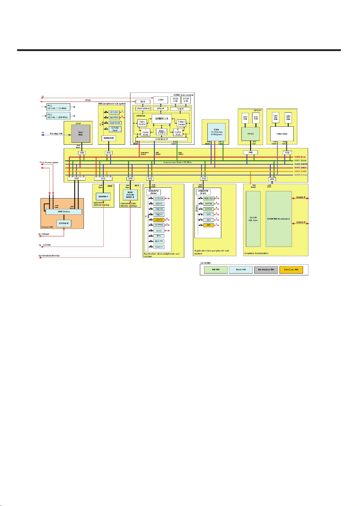
3.1 Digital Baseband(DBB) & Multimedia Processor
3.1.1 General Description
• Access subsystem
- Access Central Processing Unit (CPU) subsystem – ARM926, Joint Test Action Group (JTAG),
Embedded Trace Module (ETM), Instruction and Data (I&D)-cache, and I&D-TCM
- Access peripheral subsystems – Subscriber Identity Module (SIM) interface, IrDA®, Universal Serial
Bus (USB), Universal Asynchronous Receiver/Transmitter (UART), and so on
- Digital Signal Processor (DSP) subsystem – CEVA-X1620, JTAG, Static Random Access Memory
(SRAM), and Program Data Read Only Memory (PDROM)
- EDGE/GSM/GPRS (EGG) subsystem – EGG hardware accelerators
- WCDMA subsystem – WCDMA hardware accelerators
• Application subsystem
- Application CPU subsystem – containing ARM926, JTAG, ETM, I&D-cache, and I&D-TCM
- Application peripheral subsystems – I2C™, keypad, UART, and so on
- Graphics subsystem – XGAM subsystem
- Audio Processing Execution (APEX) and video encoder subsystems
In addition to the two subsystems above, there is also a test block, chip control block, and
a pad multiplexing block residing at the top level
y DSP
- The Digital Signal Processor Subsystem (DSPSUB) includes a DSP mega cell, which
contains the DSP CPU together with a tightly coupled memory. The DSP is the Ceva-X
1620 core with a 64 kB instruction RAM and a 64 kB data RAM. It also contains debug
logic and interfaces. In addition to the mega cell, the DSPSUB includes external memories,
peripheral units, and interfaces. The DSP mega cell is clocked at 208 MHz.
- The DSPSUB includes an AHB master and an AHB slave interface. The AHB master
provides a direct access to the Internal Random Access Memory (IRAM) in the EGG core
through the AHB. The AHB slave interface allows the CPU and the DMA to access in the
program and data RAM residing in the DSPSUB.
y WCDMA subsystem
- The digital baseband controller WCDMA subsystem incorporate a WCDMA modem
- An interface to the WCMDA together with memory control and an internal single port
RAM. The WCDMA subsystem has three AHB slave interfaces.
- The Ericsson DB 3150 also includes HSDPA class 6 functionality.
- The WCDMA subsystem is handled and provided by Ericsson.
y XGAM subsystem
- The XGAM subsystem is a graphics acceleration module that provides hardware
support in the creation of visual imagery and the transfer of this data to a display.
The XGAM also provides support for connecting a Camera module. The visual data
could be graphics, still images, or video.
- The XGAM subsystem is handled and provided by Ericsson.
y Operation and Services
- I²C™ Interface
- SIM Interfaces
- General Purpose I/O (GPIO) Interface
- External Memory Interface that supports NAND, NOR, PSRAM, SDRAM,
-JTAG
-RTC
- ETM (in Prototype Package)
LGE Internal Use Only Copyright © 2009 LG Electronics. Inc. All right reserved.
- 22 -
Only for training and service purposes
3. Technical brief
Figure 3-1-1 GD580 Block Diagram
Copyright © 2009 LG Electronics. Inc. All right reserved.
Only for training and service purposes
- 23 -
LGE Internal Use Only
3. Technical brief
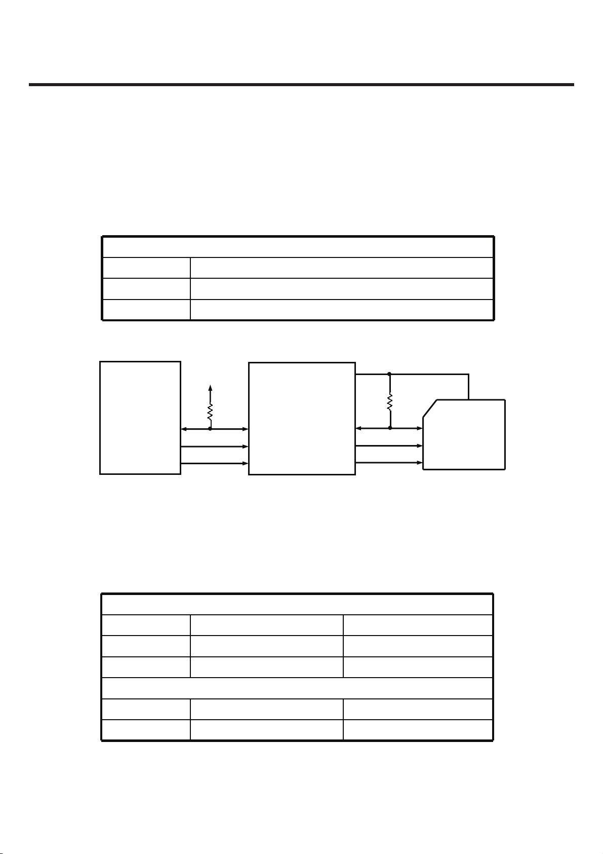
3.1.2 External memory interface
RF calibration data, Audio parameters and battery calibration data etc are stored in flash
memory area.
A. GD580
y 2Gb NAND flash memory + 1Gb SDRAM
Device Part Name Maker Item Time Size Speed
Program speed 220μs 1 page = (2K+64)Byte 2.64MByte/s
NAND flash KA100J00BA-AJYY Samsung
Erase speed 1.5ms 1 Block = (128K+4K)Byte 8MByte/s
Table 3-1-1. External Memory Interface Spec. of GD580
Figure 3-1-2. External Memory Configuration of GD580
y Package
- 107-ball FBGA Type – 10.5X13X1.2mmt, 0.8mm pitch
LGE Internal Use Only Copyright © 2009 LG Electronics. Inc. All right reserved.
- 24 -
Only for training and service purposes
3.1.3 Hardware Architecture
A. Block Diagram
3. Technical brief
Figure 3-1-3. Access system of Ericsson DB3150
Copyright © 2009 LG Electronics. Inc. All right reserved.
Only for training and service purposes
- 25 -
LGE Internal Use Only
3. Technical brief
Figure 3-1-4. Application system of Ericsson DB3150
LGE Internal Use Only Copyright © 2009 LG Electronics. Inc. All right reserved.
- 26 -
Only for training and service purposes

3. Technical brief
B. CPU Subsystem
- Access CPU subsystem
The digital baseband controller includes an access CPU subsystem, which includes the sub
modules described below.
• 32 KiB I-cache
• 16 KiB D-cache
• Page table
• Memory Management Unit (MMU)
•JTAG
•ETM9
• 26 KiB I-TCM
•8 KiBD-TCM
- Application CPU subsystem
The digital baseband controller includes an Application CPU subsystem, which includes the
sub modules described below.
• 32 KiB I-cache
• 16 KiB D-cache
• Page table
• MMU
•JTAG
•ETM9
•8 KiBI-TCM
•8 KiBD-TCM
C. Peripheral Hardware Subsystem
The digital baseband controller includes hardware that supports mobile terminal peripherals
such as a MMC, SD, UART, I2C, USB, keypad, and infrared. Collectively, this hardware
comprises the Peripheral subsystem.
The functional blocks of the Peripheral subsystem connect to the peripheral bus through four
separate bridges, which provide a simple interface to support different timing and memory
access arrangements.
D. DSP Hardware Subsystem
The Digital Signal Processor Subsystem (DSPSUB) includes a DSP mega cell, which contains
the DSP CPU together with a tightly coupled memory. The DSP is the Ceva-X 1620 core with
a 64 kB instruction RAM and a 64 kB data RAM. It also contains debug logic and interfaces. In
addition to the mega cell, the DSPSUB includes external memories, peripheral units, and
interfaces. The DSP mega cell is clocked at 208 MHz.
The DSPSUB includes an AHB master and an AHB slave interface. The AHB master provides
a direct access to the Internal Random Access Memory (IRAM) in the EGG core through the
AHB. The AHB slave interface allows the CPU and the DMA to access in the program and
data RAM residing in the DSPSUB.
E. XGAM Subsystem
The XGAM subsystem is a graphics acceleration module that provides hardware support in
the creation of visual imagery and the transfer of this data to a display. The XGAM also
provides support for connecting a Camera module. The visual data could be graphics, still
images, or video.
The XGAM subsystem is handled and provided by Ericsson.
Copyright © 2009 LG Electronics. Inc. All right reserved.
Only for training and service purposes
- 27 -
LGE Internal Use Only
3. Technical brief
F. System Control Subsystem
The SYSCON resides at the top level of the circuit architecture and is responsible for clock
generation and clock and reset distribution within the digital baseband controller, as well as to
external devices.
The block is a slave peripheral under control of the ARM processor. The programming of the
SYSCON controls the fundamental modes of operation within the digital baseband controller.
Individual blocks can also be reset and their clocks held inactive by accessing the appropriate
control registers.
3.1.4 RF Interface
A. GSM Radio Link Interface
DB3150 controls GSM RF part using these signals through GSM RF chip-RF3000.
y RF_DATA_A
y RF_DATA_B
y RF_DATA_C
y RF_DATA_STRB
RF_DATA_A
RF_DATA_B
RF_DATA_C
RF_DATA_STRB
Y4
AA2
Y3
Y2
Figure 3-1-5. Schematic of GSM RF Interface
B. WCDMA Radio Link Interface
y RF_WCDMA_PA_0_EN
y RF_WCDMA_PA_1_EN
y RF_WCDMA_DCDC_EN
y RF_WCDMA_PWRDET_EN
RF_DATA_A
RF_DATA_B
RF_DATA_C
RF_DATA_STRB
RF_WCDMA_PA_0_EN
RF_WCDMA_PA_1_EN
RF_WCDMA_DCDC_EN
RF_WCDMA_PWRDET_EN
ADC_I_NEG
ADC_I_POS
ADC_Q_NEG
ADC_Q_POS
DAC_I_NEG
DAC_I_POS
DAC_Q_NEG
DAC_Q_POS
TX_POW
Y4
AA2
Y3
Y2
AB8
V7
AB5
AB6
Y10
W10
W9
Y9
Y8
W8
W7
Y7
AB7
QDATA_AMP_MSB
IDATA_FREQ_MSB
AMP_LSB_FREQ_LSB
DCLK_DATSTR
QDATA_AMP_MSB
IDATA_FREQ_MSB
AMP_LSB_FREQ_LSB
DCLK_DATSTR
WTX_BAND_1_EN
WDCDC_EN
WPOW_DET_EN
WRX_I_N
WRX_I_P
WRX_Q_N
WRX_Q_P
WTX_I_ N
WTX_I_ P
WTX_Q_N
WTX_Q_P
WPOW_DET
Figure 3-1-6. Schematic of WCDMA RF Interface
LGE Internal Use Only Copyright © 2009 LG Electronics. Inc. All right reserved.
- 28 -
Only for training and service purposes
3.1.5 SIM Interface
SIM interface scheme is shown in Figure3-1-7.
SIMDAT0, SIMCLK0, SIMRST0 ports are used to communicate DBB(DB3150) with
ABB(AB3000) and filter.
SIM (Interface between DBB and ABB)
SIMDAT0 SIM card bidirectional data line
SIMC
LK0 SIM card reference clock
SIMRST0 SIM card async/sync reset
Table 3-1-2. SIM Interface
3. Technical brief
DB3150
SIMDAT0
SIMCLK0
SIMRST0
VDD
E
10K
SDAT SIMDAT
SCLK SIMCLK
SRST SIMRST
Figure 3-1-7. SIM Interface
SIMVCC
AB3000
3.1.6 UART Interface
UART signals are connected to DB3150 GPIO through IO connector
UART0
Resource Name Note
ACC_GPIO_2 ACC_GP02_UART0_RX ACC Receive Data
10K
VDD
DAT
CLK CARD
RST
ACC_GPIO_3 ACC_GP03_UART0_TX ACC Transmit Data
APP_GPIO_0 APP_GP00_UART_RX APP Receive Data
APP_GPIO_1 APP_GP01_UART_TX APP Transmit Data
Table 3-1-3. UART Interface
Copyright © 2009 LG Electronics. Inc. All right reserved.
Only for training and service purposes
UART1
- 29 -
LGE Internal Use Only
3. Technical brief
3.1.7 GPIO (General Purpose Input/Output) map
In total 39 allowable resources. This model is using 39 resources.
GPIO Map, describing application, I/O state, and enable level are shown in below table.
Access GPIO
GPIO Assigned Name Init Status
ACC_GPIO_0 ACC_USB_SUSPND Output low
ACC_GPIO_1 ACC_USB_PUEN output low
ACC_GPIO_2 ACC_UART0_RX Input
ACC_GPIO_3 ACC_UART0_TX output low
ACC_GPIO_4 ACC_USB_RCV Input
ACC_GPIO_5 ACC_USB_VBDET Input
ACC_GPIO_6 ACC_GP_LED_M_RES_M Output low
ACC_GPIO_7 ACC_GP_LED_M_LDO_EN Output low
ACC_GPIO_8 NA Output low
ACC_GPIO_9 ACC_GP_HF_MIC_BIAS_EN Output low
ACC_GPIO_10 NA Output Low
ACC_GPIO_11 NA Output Low
ACC_GPIO_12 ACC_GP_BT_SPI_INT Input
ACC_GPIO_13 ACC_GP_FLIPSENSE Input
ACC_GPIO_14 ACC_GP_FM_RDY Output low
ACC_GPIO_15 ACC_GP_PHFSENSE Input
ACC_GPIO_16 DCON Output low
ACC_GPIO_17 ACC_GP_VGA_SDN Output low
ACC_GPIO_18 NA Output low
ACC_GPIO_19 ACC_GP_BT_SPI_CS0N Output low
ACC_GPIO_20 ACC_GP_BT_SPI_DAT0 Input
ACC_GPIO_21 ACC_GP_BT_SPI_DAT1 Input
ACC_GPIO_22 ACC_GP_BT_SPI_CLK Output Low
ACC_GPIO_23 ACC_GP_LED_M_CTRL Output Low
Table 3-1-4. DB3150 ACC GPIO Map Table
LGE Internal Use Only Copyright © 2009 LG Electronics. Inc. All right reserved.
- 30 -
Only for training and service purposes
3.1.8 GPIO (General Purpose Input/Output) map
Application GPIO
GPIO Assigned Name Init Status
APP_GPIO_0 APP_UART_RX Input
APP_GPIO_1 APP_UART_TX Output low
APP_GPIO_2 APP_GP_3MCAM_SDN Output high
APP_GPIO_3 APP_GP_CAM_LDO_EN Output low
APP_GPIO_4 APP_GP_FM_SDA Output low
APP_GPIO_5 APP_GP_LED_M_BOOST_EN Output low
APP_GPIO_6 APP_GP_MMC_DET Input
3. Technical brief
APP_GPIO_7 APP_GP_3AXIS_INT Input
APP_GPIO_8 APP_GP_3AXIS_SDA Input
APP_GPIO_9 APP_GP_3AXIS_SCL Output high
APP_GPIO_10 APP_GP_LCD_BL_CTRL Output high
APP_GPIO_11 APP_GP_MMC_CLKRET Output low
APP_GPIO_12 APP_GP_FM_SCL Output Low
APP_GPIO_13 ACC_GP_LED_M_SDA Input
APP_GPIO_14 ACC_GP_LED_M_SCL Output Low
Table 3-1-5. DB3150 APP GPIO Map Table
Copyright © 2009 LG Electronics. Inc. All right reserved.
Only for training and service purposes
- 31 -
LGE Internal Use Only
 Loading...