

Page 1
10L 42” LCD TV Power specification
LIB.Scanning
SPECIFICATION FOR
• P/NO
Safety
APPROVAL
: LG Electronics inc.• CUSTOMER
: Power Supply Unit.• ITEM
Rev 2.1
RoHS
MODEL NAME CUSTOMER
LGD FHD LGP42-10LF
AUO FHD(HD) LGP42-10LA EAY60869403
CMO FHD LGP42-10LC EAY60869405
• DATE
• Revision
• Remark
: 2011. 04. 28
: REV 2.1
:
MP (PCB REV 1.3)
EAY60869402 PLHF-L923A
SUPPLIER
PLHF-L923B
PLHF-L923C
Producing District : LGITGJ (Jangduk-dong, Gwangju-si, Korea)
LGITYT (Yantai Shandong, China)
(생산지) (한국 광주 장덕동 / 중국 산동 연태)
★ Safety Standard Parts [안전규격부품 List ]
Power Cord, Power Plug, X/Y-Capacitor, Power Switch, Fuse, SMPS Trans, Stand-By Trans, Photo coupler,
Insulation(절연) Resistor, Discharge(방전) Resistor, Fusing Resistor, FBT.CPT, CPT Socket, DY, D-Coil, Line Filter, PCB
Material, Front / Back-cover Material Relay(1-2차간), Varistor, Adapter
★ EMC Standard Parts [전자규격 부품 List ]
Power Plug, Line Filter, X-Capacitor, Y-Capacitor, SMPS Trans, Tuner, Saw-Filter, Shield Case, Oscillator, Pattern
Change
★ Green [유해물질 확인사항]
This item must meet the standards of LG Electronics for six major substances as designated by RoHS for control.
(Cd: 10ppm under, Pb/Hg/Cr+6/PBB/PBDE: 100 ppm under)
PLHF-L923A/B/C (REV.2.1)
LG Innotek Co., Ltd
LG Twin Tower 33/34F, Yeouido-dong,
Yeongdeungpo-gu, Seoul, Korea
Tel. : +82-2-3777-1114
Fax. : +82-2-3777-0082
1
Date: 2011. 04. 28
Page 2
10L 42” LCD TV Power specification
Documentation For
Rev 2.1
DOCUMENT NO : PLHF-L923A/B/C
Approval
Description Model Name
LGD FHD LGP42-10LF
AUO FHD(HD) LGP42-10LA EAY60869403
CMO FHD LGP42-10LC EAY60869405
Written Checked Approved
LGE P/No.
EAY60869402
신광철 최광탁 이영수
PLHF-L923A/B/C (REV.2.1)
2
Date: 2011. 04. 28
Page 3
10L 42” LCD TV Power specification
NO. A table of contents Page
1 Documentation of Approval 1~2
2 Contents 3
3 Revision History 4~5
4 CTQ Management & Differentia & Model Marking 6~8
Specification
1. INTRODUCTION
2. SPECIFICATION
2.1 Input Requirements
2.2 Power Output Characteristics
2.3 Inverter Output Characteristics
2.4 Environment Requirement
2.5 Dielectric Strength Voltage and Insulation Resistance
2.6 Burn-in
5
2.7 Interface
2.8 Product Safety
2.9 Construction
2.10 Function of protection
2.11 Sound Noise Characteristics
2.12 Connector Specification
2.13 Inverter Test Method
2.14 PCB Dimension
2.15 Apply to Eyelet Point
2.16 Electrical Characteristics
2.17 Mechanical Characteristics
Rev 2.1
Contents
9~27
6 Schematic Diagram 28~31
7 Block Diagram 32~33
8 Parts List 34~58
9 Process Marking 59~60
10 PCB Layout 61~65
11 Safety Parts 66~68
12 Mechanical Drawing 69~75
13 Packing Drawing 76~81
14 Bar-code Label Drawing 82~85
15 Labeling Point 86~87
16 Workmanship Point 88~91
17 * Appendix
A1. PCB Check list
A2. Warranty letter
92~
PLHF-L923A/B/C (REV.2.1)
3
Date: 2011. 04. 28
Page 4
10L 42” LCD TV Power specification
Rev 2.1
Revision History
Rev No. Contents
0.2
0.3
Apply to PQ (PCB REV 0.7)
PCB P/No.:EAX61124201/9
Apply to PQ (PCB Rev. 0.8)
PCB P/No.:EAX61124201/10
# Improvement EMI
1. LB701, LB702 : Bead Jumper
2. LB703, LB704 : Jumper Bead
3. C720,721 : 100p N.C
4. C706, C707 : Add 100p
# Improvement Q502 TR Margin
5. R506 : 100K N.C
6. R502 : N.C 100K
Date of
approval
09. 10. 30
09. 11. 11
Checked Remark
0.4
# AC Brownout change
7. R519 : 2.2M 1M
8. R513,R514,R515,R516,R517,R518, R509
: J(5%) F(1%) Grade Change
9. C509 : 22uF 10uF
10. C502: 0.68uF 0.1uF
# Location change
11. VA100, CX101
Apply to PQ (PCB Rev. 0.9)
PCB P/No.:EAX61124201/11
1. SK101 add GND Area
# Improvement 3.5V & 12V Overshooting
2. R218 : 1K J 4.7K J
3. C221 : 50V 1uF Add
Apply to MP-Limit (PCB Rev. 1.0)
PCB P/No.:EAX61124201/13
09. 11. 23
1.0
# Improvement EMI
1. C714, 715 : 0.001uF NC
# Delete Jump wire
2. Delete J7, J39
PLHF-L923A/B/C (REV.2.1)
09. 12. 07
4
Date: 2011. 04. 28
Page 5
10L 42” LCD TV Power specification
Rev 2.1
Rev No. Contents
Apply to MP-Limit (PCB Rev. 1.1)
PCB P/No.:EAX61124201/14
# Improvement Inverter Margin
1.1
1.2
42AUO(EAY60869403)
1. 1. R301 : 27K/F => 27K/J
2. R302 : 75K/F => 51K/J
3. R328 : 36/F => N.C
4. VR301 : N.C => 10K
5. Operating Frequency : 62kHz ± 2kHz => 62kHz ± 1kHz
Apply to MP (PCB Rev. 1.2)
PCB P/No.:EAX61124201/15
1. Location for Barcode Label changed. (on the HS3)
Revision History
Date of
approval
10. 1. 7
10. 1. 25
Checked Remark
1.3 1. Addition for CMO Model 10. 3. 15
Apply to MP (PCB Rev. 1.2)
PCB P/No.:EAX61124201/15
1. Add to Material Supply Vendor
1) Flux: Alpha Metal Alpha Metals, 동화다무라, 청솔
2) Silicon Bond: OKONG (For Auto Dispensor)
3) PCB: Huiho, Hsiang Kuo, Samhan, Daeduck, Chin Poon
Huiho, Hsiang Kuo, Samhan, Daeduck, Chin Poon, WeiJum
1.4
2. Change to Eyelet Shape (Prevent to fuse lead insert missing)
- Shape: Eyelet Gripper (Φ1.6*2.6L)
- Location No: EL19, EL20, EL54, EL56
3. Change to Line Filter Bobbin Color (Prevent to mix other parts)
- Color: White Black
- Location No.: LF102, LF103
- Part No.: LLF-104
- Vendor: Clover Hitek, SooJung
10. 7. 8
923C
Only
MP limit
Qty:30K
Apply to MP (PCB Rev. 1.2)
PCB P/No.:EAX61124201/15
1.Add to Material Supply Vendor (To Improvement component
1.5
1)Location Number : D501,D502,D504 (UF4007/UF1007/HER108G)
2)Maker : TSC,Fairchild,RECTRON TSC,Fairchild,RECTRON,Diodes
delivery)
PLHF-L923A/B/C (REV.2.1)
10.07.23
5
Date: 2011. 04. 28
Page 6
10L 42” LCD TV Power specification
Rev 2.1
Revision History
Rev No. Contents
Apply to MP (PCB Rev. 1.2)
PCB P/No.:EAX61124201/15
1.Add to Material (To Improvement component delivery)
1)Location Number : D202
2)
MBRF20U65CT, KEC
1.6
FMW-2206, SANKEN
MBRF2060CT, SENSITRON
2. Add to Material Supply Vendor
1) CX101, CX102 : Pilkor Pilkor, OKAYA, Europtronic
Apply to MP (PCB Rev. 1.2)
PCB P/No.:EAX61124201/15
MBRF20U65CT, KEC
FMW-2206, SANKEN
MBRF2060CT, SENSITRON
MBRF2060CTL, SENSITRON
Date of
approval
10.08.06
Checked Remark
CX101,
CX102
923A
Only
1.7
1.8
1.Add to Material product line (To Improvement component
delivery)
1)Location Number : IC501 (STR-W6053N)
2)Plant site
石川 Sanken(株)
Apply to MP (PCB Rev. 1.3)
PCB P/No.:EAX61124201/16
1. PCB change for PL prevention.
Apply to MP (PCB Rev. 1.3)
PCB P/No.:EAX61124201/16
石川 Sanken(株)
鹿島 Sanken(株)
10.08.14
10.09.17
1.9
1. Change to Line Filter Bobbin Color (Prevent to mix other parts)
- Color: White Black
- Location No.: LF102, LF103
- Part No.: LLF-104
- Vendor: Clover , SooJung , Feelux
PLHF-L923A/B/C (REV.2.1)
11.03. 24
6
Date: 2011. 04. 28
Page 7
10L 42” LCD TV Power specification
Rev 2.1
Rev No. Contents
Apply to MP (PCB Rev. 1.3)
PCB P/No.:EAX61124201/16
2.0
1. Add to Material Supply Vendor
1) Silicon Bond : DONGYANG
2) Jumper Wire : ILKWANG
Apply to MP (PCB Rev. 1.3)
PCB P/No.:EAX61124201/16
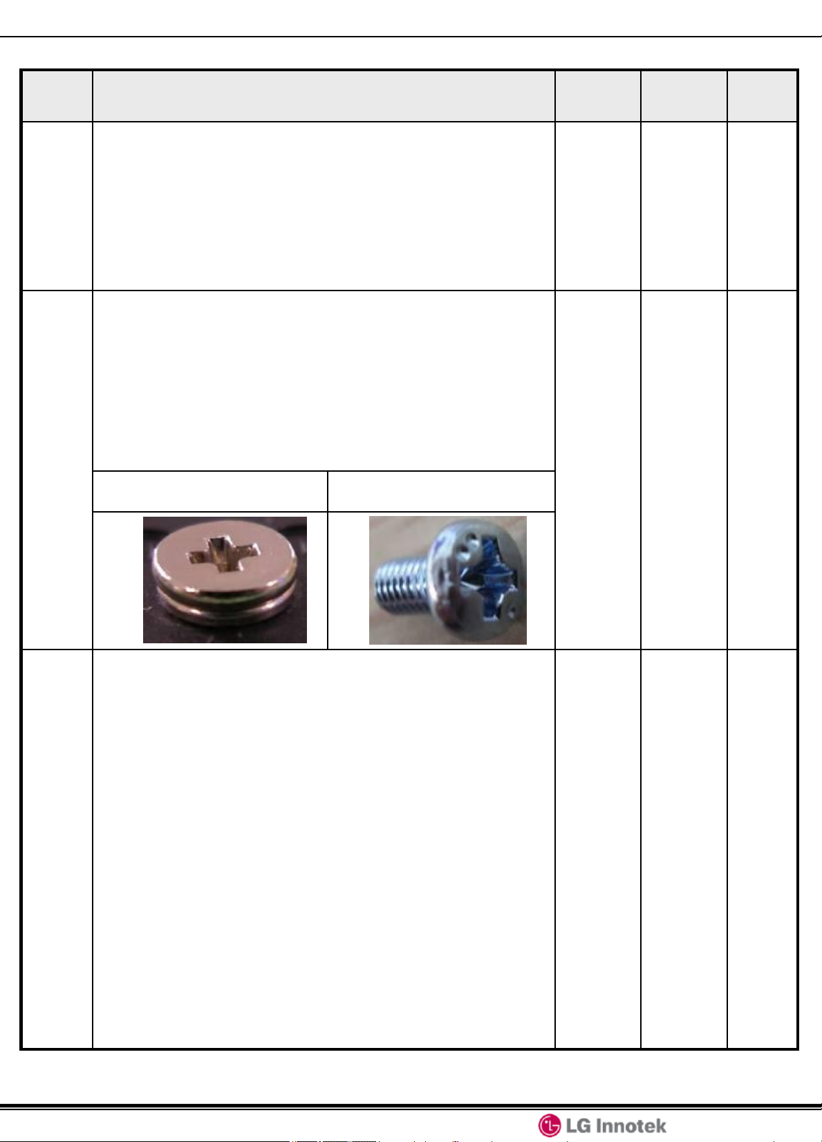
# Add screw type.
Before : SCREW PH S+P/W MACHINE M3X10 / 12
After :
- SCREW PH S+P/W MACHINE M3 X10 / 12
- BHM Screw, M3.0 * 8.0 / 9.0L, with Clamfix,Cr3+WH Plating
* Apply for all screw.
2.1
Before After [ ADD ]
Date of
approval
11.03.31 G. T. Choi
11.04.28 G. T. Choi
Checked Remark
PLHF-L923A/B/C (REV.2.1)
7
Date: 2011. 04. 28
Page 8
10L 42” LCD TV Power specification
CTQ Management
No. Contents Page
1 2.1.1 Power Factor 10
2 2.2 Power Output Characteristics 11
3 2.2.1. Stand by Power Consumption 11
4 2.3 Inverter Output Characteristics 12~14
5 Additional Soldering point 85
Rev 2.1
PLHF-L923A/B/C (REV.2.1)
8
Date: 2011. 04. 28
Page 9
10L 42” LCD TV Power specification
Rev 2.1
Differentia
Model
Details
T703,
T704
R301 RES FLAT 39K F 1/8 (2012) RES FLAT 27K J 1/8 (2012) RES FLAT 27K J 1/8 (2012)
R302 RES FLAT 62K F 1/8 (2012) RES FLAT 51K J 1/8 (2012) RES FLAT 51K J 1/8 (2012)
R306 RES FLAT 150K J 1/8 (2012) RES FLAT 100K J 1/8 (2012) RES FLAT 200K J 1/8 (2012)
R308 RES FLAT 10K F 1/8 (2012) RES FLAT 6.8K F 1/8 (2012) RES FLAT 7.5K F 1/8 (2012)
R322 RES FLAT 6.2K F 1/8 (2012) RES FLAT 5.1K F 1/8 (2012) RES FLAT 6.2K F 1/8 (2012)
R323 RES FLAT 6.8K F 1/8 (2012) RES FLAT 6.8K F 1/8 (2012) RES FLAT 10K F 1/8 (2012)
R325 RES FLAT 9.1K J 1/8 (2012) RES FLAT 5.1K J 1/8 (2012) RES FLAT 20K J 1/8 (2012)
R327 RES FLAT 10K J 1/8 (2012) RES FLAT 4.7K J 1/8 (2012) RES FLAT 12K J 1/8 (2012)
C401 22pF J 6KV (10mm) 5pF J 6KV (10mm) 10pF J 6KV (10mm)
C402 54pF J 6KV (10mm) 39pF J 6KV (10mm) 54pF J 6KV (10mm)
C403
CAP FLAT 47nF K 50V X7R
LGP42-10LF
(EAY60869402)
LIF42-100L LIF42-101A LIF42-102C
CAP FLAT 47nF K 50V X7R
(2012)
LGP42-10LA
(EAY60869403)
(2012)
LGP42-10LC
(EAY60869405)
CAP FLAT 56nF K 50V X7R
(2012)
C404
C405
C406
EL70 EYELET DIA 1.6*3.0 N.C N.C
EL71 N.C EYELET DIA 1.6*3.0 N.C
EL72 N.C N.C EYELET DIA 1.6*3.0
CAP FLAT 15nF K 50V X7R
(2012)
CAP FLAT 15nF K 50V X7R
(2012)
CAP FLAT 15nF K 50V X7R
(2012)
CAP FLAT 5.6nF K 50V X7R
(2012)
CAP FLAT 5.6nF K 50V X7R
(2012)
CAP FLAT 5.6nF K 50V X7R
(2012)
CAP FLAT 27nF K 50V X7R
(2012)
CAP FLAT 6.8nF K 50V X7R
(2012)
CAP FLAT 6.8nF K 50V X7R
(2012)
PLHF-L923A/B/C (REV.2.1)
9
Date: 2011. 04. 28
Page 10
10L 42” LCD TV Power specification
Rev 2.1
Marking for Model
LGD FHD :
EAY60869402
LGD FHD Only
EL70 Eyelet
AUO FHD :
EAY60869403
AUO FHD Only
EL71 Eyelet
CMO FHD :
EAY60869405
CMO FHD Only
EL72 Eyelet
PLHF-L923A/B/C (REV.2.1)
10
Date: 2011. 04. 28
Page 11
10L 42” LCD TV Power specification
Specification
Rev 2.1
PLHF-L923A/B/C (REV.2.1)
11
Date: 2011. 04. 28
Page 12
10L 42” LCD TV Power specification
1. INTRODUCTION
1.1 Scope
This approval is the description related to every electrical and structural specifications
and reliability For Power Supply Unit (LGD FHD : LGP42-10LF, AUO FHD(HD) : LGP42-10LA,
CMO FHD : LGP42-10LC ) used on 42 inch LGE LCD TV.
1.2 Customers product related items
Product : Power Supply Unit
Part code : LGD FHD : EAY60869402, AUO FHD(HD) : EAY60869403,
CMO FHD : EAY60869405
1.3 Product name
Product name : LGD FHD : PLHF-L923A, AUO FHD(HD) : PLHF-L923B,
CMO FHD : PLHF-L923C
Revision code : 2.0
2. SPECIFICATION
Rev 2.1
2.1 Input Requirements
Nominal Input Voltage AC 100V to AC 240V
Input Voltage Variation AC 90V to AC 264V
Under 3.5Arms . (at 100Vac & Nominal Load)
Input Current
Under 1.5Arms . (at 240Vac & Nominal Load)
Nominal Frequency 50 / 60 Hz
Frequency Variation Range 47 Hz to 63 Hz
Phase Single
Leakage Current 0.7mA_peak. (100Vac ~ 240Vac)
Surge Immunity
± 4kV / 1000ns / 0˚ to 360˚
Hold-up Time More than 20ms at 100Vac and maximum output load
Lightning Surge 2kA Normal, Common Mode
Inrush Current
2.1.1 Power Factor
Over than 0.9 at 90 – 264Vac & max load condition
PLHF-L923A/B/C (REV.2.1)
80A zero-pk max
at cold start and any specified line, load, and temperature
conditions.
12
Date: 2011. 04. 28
Page 13
10L 42” LCD TV Power specification
2.2 Power Output Characteristics
Rev 2.1
Output
Voltage
Variable range
[V]
Rated Current
(Min, Max)
[Amean]
0.3W Under(15mA)
Voltage
Regulation
[V]
- -
Ripple
Voltage
[mVp_p]
3.5V
(ST-BY)
3.23V ~ 3.57V
1.9A (0.8~1.9)
- 250 mVp_p
(ON condition)
12V 11.4V ~ 12.6V 2.8A (0.35~2.8) ± 5% 350 mVp_p
20V 17V ~ 25.2V 1.1A (0.07~1.1) -15% ~ +26% 500 mVp_p
* On Condition : In a moment of Power_ON Signal activated, the current of 3.5V output
should be limited within 40mA(Max) at LCD TV condition for stability.
Do not turn “Power_ON” Signal on at the load condition of 3.5V output, more than 40mA.
* Total regulation for each output circuit includes the results of input voltage variation,
load variation, warm-up drift and temperature change.
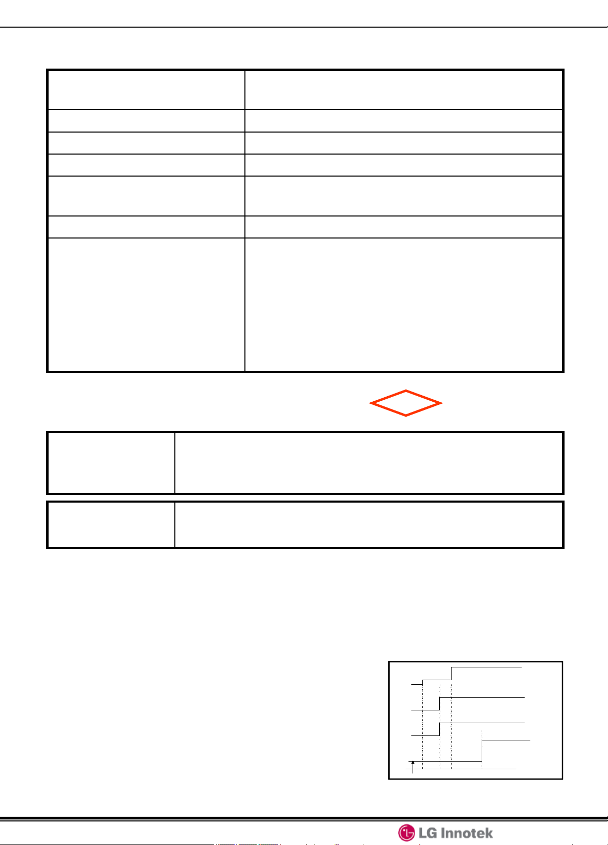
* The following instruments shall be used for measuring ripple noise.
1. Probe having impedance ratio of 1:1.
2. Oscilloscope having frequency characteristic of 100MHz or more.
Test Point : power output 각 pin
Add Electrolytic Capacitor 47㎌ + 0.1㎌
Power Supply Unit
Output Voltage
700mm
※ Ripple and noise are measured at the end of output cable which are added a 0.1uF ceramic
capacitor and 47uF electrolytic capacitor. ( connected parallel )
+
Load
Oscilloscope
Measurement point
2.2.1 Stand By Power Consumption
Output Voltage 3.5V (STBY) 12V 20V
Load [A] 0.015
Wattage [W] Less than 0.3 Under (230Vac / 50Hz)
PLHF-L923A/B/C (REV.2.1)
13
Don’t Care (Power-Off)
Date: 2011. 04. 28
Page 14
10L 42” LCD TV Power specification
2.3 Inverter Output Characteristics
“When doing inverter test, GND should be reinforced”
2.3.1 LGD FHD LGP42-10LF (EAY60869402)
Item Symbol Condition Min Typ Max Unit Remarks
Rev 2.1
PFC
Voltage
Control
Voltage
Input
Current
Input
Power
Back light
ON/OFF
Control
Analog
Dimming
Control
VPFC
VC
Iin
(Max)
Pin
Lamp ON=High 3.0 3.3 5.0
VON/OFF
Lamp OFF=Low 0.0 - 0.8
A-DIM - - 1.65 3.3 Vdc
- 380 390 400
- 11.4 12 12.6
Vin=390V,
A-DIM=1.65V
B-DIM=3.3V
Vin=390V,
A-DIM=1.65V,
B-DIM=3.3V
- 0.4 - Arms -
- 154 - W -
1차측(HOT)
Vdc
2차측(COLD)
Vdc -
1.65V : Normal
3.3V : 매장mode
Lamp
Voltage
Lamp
Current
PWM Duty
Ratio
Operating
Frequency
Open Lamp
Voltage
Striking time Ts 1.5 - 3.0 sec -
Vout
(Normal)
Iout
(Normal)
Iout
(Min)
Iout
(Max)
Fo
Vopen
A-DIM=1.65V
B-DIM=3.3V
A-DIM=1.65V
B-DIM=3.3V
B-DIM=3.3V
(Input Duty : 20%)
B-DIM=3.3V
(Input Duty : 100%)
A-DIM=1.65V
B-DIM=3.3V
No load,
Vin=390V,
A-DIM=1.65V
B-DIM=3.3V
840 1040 1240 Vrms
123 136 149 mArms EEFL:16ea
5 10 15
%
100 - -
47 48.5 50 KHz -
1125 - - Vrms One side
One side
2시간 Aging후
Output Current
기준
(120Hz)
PLHF-L923A/B/C (REV.2.1)
14
Date: 2011. 04. 28
Page 15
10L 42” LCD TV Power specification
“When doing inverter test, GND should be reinforced”
2.3.2 AUO FHD(HD) LGP42-10LA (EAY60869403)
Item Symbol Condition Min Typ Max Unit Remarks
Rev 2.1
PFC
Voltage
Control
Voltage
Input
Current
Input
Power
Back light
ON/OFF
Control
Analog
Dimming
Control
VPFC
VC
Iin
(Max)
Pin
Lamp ON=High 3.0 3.3 5.0
VON/OFF
Lamp OFF=Low 0.0 - 0.8
A-DIM - - 1.65 3.3 Vdc
- 380 390 400
- 11.4 12 12.6
Vin=390V,
A-DIM=1.65V
B-DIM=3.3V
Vin=390V,
A-DIM=1.65V,
B-DIM=3.3V
- 0.8 - Arms -
- 108 - W -
1차측(HOT)
Vdc
2차측(COLD)
Vdc -
1.65V : Normal
3.3V : 매장mode
Lamp
Voltage
Lamp
Current
PWM Duty
Ratio
Operating
Frequency
Open Lamp
Voltage
Striking time Ts 1.5 - 3.0 sec -
Vout
(Normal)
Iout
(Normal)
Iout
(Min)
Iout
(Max)
Fo
Vopen
A-DIM=1.65V
B-DIM=3.3V
A-DIM=1.65V
B-DIM=3.3V
B-DIM=3.3V
(Input Duty : 20%)
B-DIM=3.3V
(Input Duty : 100%)
A-DIM=1.65V
B-DIM=3.3V
No load,
Vin=390V,
A-DIM=1.65V
B-DIM=3.3V
750 950 1150 Vrms
125 135 145 mArms EEFL:14ea
5 10 15
%
100 - -
61 62 63 KHz -
1480 - - Vrms One side
One side
2시간 Aging후
Output Current
기준
(120Hz)
PLHF-L923A/B/C (REV.2.1)
15
Date: 2011. 04. 28
Page 16

10L 42” LCD TV Power specification
“When doing inverter test, GND should be reinforced”
2.3.3 CMO FHD LGP42-10LC (EAY60869405)
Item Symbol Condition Min Typ Max Unit Remarks
Rev 2.1
PFC
Voltage
Control
Voltage
Input
Current
Input
Power
Back light
ON/OFF
Control
Analog
Dimming
Control
VPFC
VC
Iin
(Max)
Pin
Lamp ON=High 3.0 3.3 5.0
VON/OFF
Lamp OFF=Low 0.0 - 0.8
A-DIM - - 1.65 3.3 Vdc
- 380 390 400
- 10.8 12 13.2
Vin=390V,
A-DIM=1.65V
B-DIM=3.3V
Vin=390V,
A-DIM=1.65V,
B-DIM=3.3V
- 0.52 - Arms -
- 130 150 W -
1차측(HOT)
Vdc
2차측(COLD)
Vdc -
1.65V : Normal
3.3V : 매장mode
Lamp
Voltage
Lamp
Current
PWM Duty
Ratio
Operating
Frequency
Open Lamp
Voltage
Striking time Ts 1.5 - 3.0 sec -
Vout
(Normal)
Iout
(Normal)
Iout
(Min)
Iout
(Max)
Fo
Vopen
A-DIM=1.65V
B-DIM=3.3V
A-DIM=1.65V
B-DIM=3.3V
B-DIM=3.3V
(Input Duty : 20%)
B-DIM=3.3V
(Input Duty : 100%)
A-DIM=1.65V
B-DIM=3.3V
No load,
Vin=390V,
A-DIM=1.65V
B-DIM=3.3V
890 1060 1290 Vrms
115 125 135 mArms EEFL:14ea
5 10 15
%
100 - -
61 62 63 KHz -
1600 - - Vrms One side
One side
2시간 Aging후
Output Current
기준
(120Hz)
PLHF-L923A/B/C (REV.2.1)
16
Date: 2011. 04. 28
Page 17
10L 42” LCD TV Power specification
Load 부가 순서 : T1T2T3T4
T2 : Min 10ms
T3 : Min 5ms
10L Aging Sequence
0.1A
Full load 80%
3.5V
20V
12V
인버터
Full load 80%
Full load 80%
Full load 80%
T1
T2 T3
T4
Ac Power ON
Load 부가 순서 : T1T2T3T4
T2 : Min 10ms
T3 : Min 5ms
10L Aging Sequence
0.1A
Full load 80%
3.5V
20V
12V
인버터
Full load 80%
Full load 80%
Full load 80%
T1
T2 T3
T4
Ac Power ON
2.4 Environment Requirement
Operating Temperature Range -10℃ to 40℃
Operating Humidity Range 30 to 85 %
Storage Temperature Range -25 to 85 deg.
Storage humidity Range 5 to 90 %
Rev 2.1
(60℃:No Hardware Failure, TV SET Condition)
MTBF
50,000 hour
(Mean Time Between Failure)
Cooling Condition Natural Air
Shock 98 ㎨
Shock test consists of pivoting the power supply,
from one edge of it’s bottom side, on a flat surface
(such as wood having thickness of 10mm or more)
and allowing the opposite edge to fall from a height
of 50mm to this surface.
The test is performed three times on each edge of
the bottom side of the power supply
2.5 Dielectric Strength Voltage and Insulation Resistance
Dielectric
Strength Voltage
AC-DC 1.5K VAC 3 SEC 10 mA.
Between Primary and All Secondary Circuits.
Safety
Insulation
Resistance
* Above tests are performed at room temperature in non-condensing atmospheric
conditions
* Frame grounds are connected to secondary circuits.
2.6 Burn-in
More than 1 hours at 45℃(±5℃), Normal input voltage.
AC on/off must be test 1 time after burn-in.
PLHF-L923A/B/C (REV.2.1)
80% Load of specification.
Insulation resistance shall be more than 8M ohm (at DC 500V)
Between Primary Live, Neutral line and Secondary.
17
Date: 2011. 04. 28
Page 18
10L 42” LCD TV Power specification
2.7 Interface
Appellation Explanation Signal Direction Action
Rev 2.1
POWER ON Vcc Circuit ON/OFF Input
Hi : Vcc ON
Low : Vcc OFF
2.8 Product Safety
Safety
Design to meet the requirements as follows
Safety Standards to be applied
UL60950, IEC60950, IEC60065 and 60950
Design to meet the requirements as follows
EMI/RFI Standards to be applied
FCC and EN55020, EN55013 Class B
with 4dB minimum margin.
2.9 Construction
Weight Less than 1.0kg
Unit Size 196(W) X 246(D) X 21(H, Max, Tolerance ±2mm)
2.10 Function of protection
Protection Output Circuit Trip point Notes
STBY 3.5V 12A ~ Latch
Over Current
12V 6A ~ Latch
20V 3A ~ Latch
STBY 3.5V - Latch
Short Circuit
12V - Latch
20V - Latch
* This Power Supply has above-mentioned protections.
* Short circuit protection between different output terminals is not considered.
* Trip point for over voltage indicates the operating point when the output voltage
slowly increases.
* The conditions of Over Current measurement
Multi output(3.5V,12V,20V) is nominal load state except an over current
measurement.
PLHF-L923A/B/C (REV.2.1)
18
Date: 2011. 04. 28
Page 19
10L 42” LCD TV Power specification
2.11 Sound Noise Characteristics
PSU Noise Specification
22.5 dB(a) / 20.u Pa 2.0E-5 Pa
(1/1 octave, A-weighting, to 1khz ~ 16khz Total overall
Measure Location : Anechoic Room
Measure Condition : At a distance of 60cm mic
Full white pattern, at AC 110V/220V
The max specification
(measure 3 points, at PSU center and left & right on the side)
Rev 2.1
2.12 Connector Specification
2.12.1 Connectors Usage
SK101 (Option 1)
Type : (DAC – 11PM1)
Maker : (Dongil)
Pin No. Signal
1 LIVE
2 F.G
3 NEUTRAL
SK102 (Option 2)
Type : (YW396-03AV)
Maker : (YEONHO)
Pin No. Signal
1 LIVE
2 NC
3 NEUTRAL
P201
Type : (FW20020-24SB), Maker : (FOOSUNG/Yeonho)
Pin No. Signal Pin No. Signal
1
3
5
7
9
11
13 GND 14
15 GND 16
17 12V 18
19 12V 20
21 12V 22
23 NC 24 ERROR
Power-ON
20V
GND
GND
3.5V
3.5V
2
4
6
8
10
12
20V
20V
GND
GND
3.5V
3.5V
GND
GND
INV ON/OFF
A-DIM
P-DIM
PLHF-L923A/B/C (REV.2.1)
19
Date: 2011. 04. 28
Page 20
10L 42” LCD TV Power specification
2.12.2 Connector Usage
2.12.2.1 Output Connector P402 : Yeonho 35002WR-02L(P)
Pin No. Symbol Color Description
Rev 2.1
P402
1 HV_2
White
High Voltage Terminal
2 HV_2 High Voltage Terminal
2.12.2.2 Output Connector P401 : Yeonho 35002WR-02L(BK)
Pin No. Symbol Color Description
P401
1 HV_1
Black
High Voltage Terminal
2 HV_1 High Voltage Terminal
PLHF-L923A/B/C (REV.2.1)
20
Date: 2011. 04. 28
Page 21
10L 42” LCD TV Power specification
2.13 Inverter Test Method.
VOLTAGE PROBE
P6015A 또는 동등품
P402
INVERTER
TRANSFORMER
INVERTER + POWER BOARD
P201
Rev 2.1
CONTROL SIGNAL
PWR ON : 3.3V
INV ON : 3.3V
PDIM : 0~3.3V
ADIM : 1.65V(Max 3.3V)
VOLTAGE PROBE
P6015A 또는 동등품
INVERTER
CONNECTION
WIRE
CURRENT PROBE : P6022A 또는 동등품
P401
INVERTER
TRANSFORMER
10LF : 500pF 6KV
10LA : 350pF 6KV
10LC : 300pF 6KV
10LF : 500pF 6KV
10LA : 350pF 6KV
10LC : 300pF 6KV
SK101
2.3㏀ / 500W
2.3㏀ / 500W
AC INPUT
PLHF-L923A/B/C (REV.2.1)
21
Date: 2011. 04. 28
Page 22
10L 42” LCD TV Power specification
2.14 PCB Dimension
▶ Components Height
Max 21mm (Tolerance ±2mm)
Rev 2.1
PCB : 1.6mm
196mm
10mm
ø4
ø4
246mm
4.5mm
4.5mm
10mm
ø4
ø4
ø4
4.5mm
4.5mm
▶ PCB Bending : Under 3.0mm
▶ Lead Cutting : Under 3.0mm
PLHF-L923A/B/C (REV.2.1)
22
ø4.5
4.5mm
4.5mm
Date: 2011. 04. 28
Page 23
10L 42” LCD TV Power specification
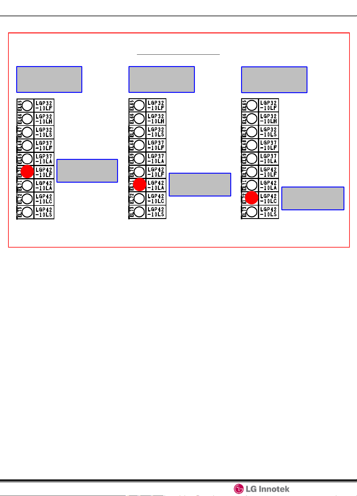
2.15 Apply to Eyelet Point
▶ LGP42-10LF
▶ Apply to Eyelet Point 2.3ø :
EL1, EL4, EL5, EL6, EL7, EL8, EL9, EL10, EL11, EL12, EL13, EL15, EL17, EL37, EL40, EL51,
EL52 (17EA)
▶ Apply to Small Eyelet 1.6ø :
EL14, EL16, EL21, EL22, EL23, EL24, EL26, EL27, EL28, EL29, EL30, EL31, EL32, EL33, EL34,
EL35, EL36, EL38, EL39, EL41, EL42, EL43, EL44, EL45, EL46, EL47, EL48, EL49, EL50, EL53,
EL55, EL57, EL58, EL63, EL64, EL70 (36EA)
▶ Apply to Griper Point 1.6ø * 2.6L:
EL18, EL19, EL20, EL25, EL54, ,EL56 (6EA)
Rev 2.1
PLHF-L923A/B/C (REV.2.1)
23
Date: 2011. 04. 28
Page 24

10L 42” LCD TV Power specification
▶ LGP42-10LA
▶ Apply to Eyelet Point 2.3ø :
EL1, EL4, EL5, EL6, EL7, EL8, EL9, EL10, EL11, EL12, EL13, EL15, EL17, EL37, EL40, EL51,
EL52 (17EA)
▶ Apply to Small Eyelet 1.6ø :
EL14, EL16, EL21, EL22, EL23, EL24, EL26, EL27, EL28, EL29, EL30, EL31, EL32, EL33, EL34,
EL35, EL36, EL38, EL39, EL41, EL42, EL43, EL44, EL45, EL46, EL47, EL48, EL49, EL50, EL53,
EL55, EL57, EL58, EL63, EL64, EL71 (36EA)
▶ Apply to Griper Point 1.6ø * 2.6L:
EL18, EL19, EL20, EL25, EL54, ,EL56 (6EA)
Rev 2.1
PLHF-L923A/B/C (REV.2.1)
24
Date: 2011. 04. 28
Page 25

10L 42” LCD TV Power specification
▶ LGP42-10LC
▶ Apply to Eyelet Point 2.3ø :
EL1, EL4, EL5, EL6, EL7, EL8, EL9, EL10, EL11, EL12, EL13, EL15, EL17, EL37, EL40, EL51,
EL52 (17EA)
▶ Apply to Small Eyelet 1.6ø :
EL14, EL16, EL21, EL22, EL23, EL24, EL26, EL27, EL28, EL29, EL30, EL31, EL32, EL33, EL34,
EL35, EL36, EL38, EL39, EL41, EL42, EL43, EL44, EL45, EL46, EL47, EL48, EL49, EL50, EL53,
EL55, EL57, EL58, EL63, EL64, EL72 (36EA)
▶ Apply to Griper Point 1.6ø * 2.6L:
EL18, EL19, EL20, EL25, EL54, ,EL56 (6EA)
Rev 2.1
PLHF-L923A/B/C (REV.2.1)
25
Date: 2011. 04. 28
Page 26
10L 42” LCD TV Power specification
2.16 Electrical Characteristics
No. Test Item Test method
Rev 2.1
Intermittent
1
Operation stability
Test
Low temperature
2
operation
Low temperature
3
Storage test Leave
At low temperature
The switching regulator shall ON/OFF for 20,000 time at an
Interval of 10 sec at maximum load, after that electrical
Characteristics shall be satisfied.
The switching regulator is left at the operating guarantee
Minimum temperature for 2 hours without applying electricity.
After that power shall be turned on, and then the electrical
Characteristics shall be satisfied.
The switching regulator is left at minimum storage
Temperature for 96 hours or more.
Then the switching regulator is left at a room temperature
and humidity for 1 hour or more, after that electrical
characteristics shall be satisfied.
The switching regulator is 10 consecutive temperature cycle
that shown below is performed and then leave them at room
temperature and humidity for 1 hour or more.
After that, electrical characteristics shall be satisfied.
Time Temperature
Heat cycle storage
4
test
5 Heat shock test
30 minutes 25℃
30 minutes 25℃ -> -20℃
60 minutes Minimum storage temperature (-20℃)
30 minutes -20℃ -> 25℃
30 minutes 25℃
30 minutes 25℃ -> 70℃
60 minutes Maximum storage temperature (70℃)
30 minutes 70℃ -> 25℃
Heat shock test performed under following conditions without
applying electricity and then leave them at room temperature
and humidity for 1 hour or more.
After that, electrical characteristics shall be satisfied.
Condition : -45℃(30minutes), 120℃(30minutes),
Switching time : Less than 5 minutes, 200 cycles.
PLHF-L923A/B/C (REV.2.1)
26
Date: 2011. 04. 28
Page 27
10L 42” LCD TV Power specification
2.17 Mechanical Characteristics
No. Test Item Test method
1 Appearance
Rev 2.1
There shall be no contaminant or dirt on the switching
regulator which has adverse effect on electrical
characteristics.
There shall be no excessive unevenness or scratches on the
plated or painted surface.
While applying electricity :
Vibration frequency : 5 ~ 100Hz
Acceleration : 4.9 m/s∧2
Vibration in X,Y,Z direction for 30 minutes
2 Vibration
3 Shock
While applying electricity :
Vibration frequency : 5 ~ 100Hz
Acceleration : 14.7 m/s∧2
Vibration in X,Y,Z direction for 30 minutes
After that electrical characteristics shall be satisfied.
There shall be no damage to appearance and construction.
Shock : 98 m/s∧2
On the oak more than 10mm thickness with the flat face,
raise the one side for 50mm, and it carries out each side
free fail for three sides.
There shall be no damage to appearance and construction.
PLHF-L923A/B/C (REV.2.1)
27
Date: 2011. 04. 28
Page 28
10L 42” LCD TV Power specification
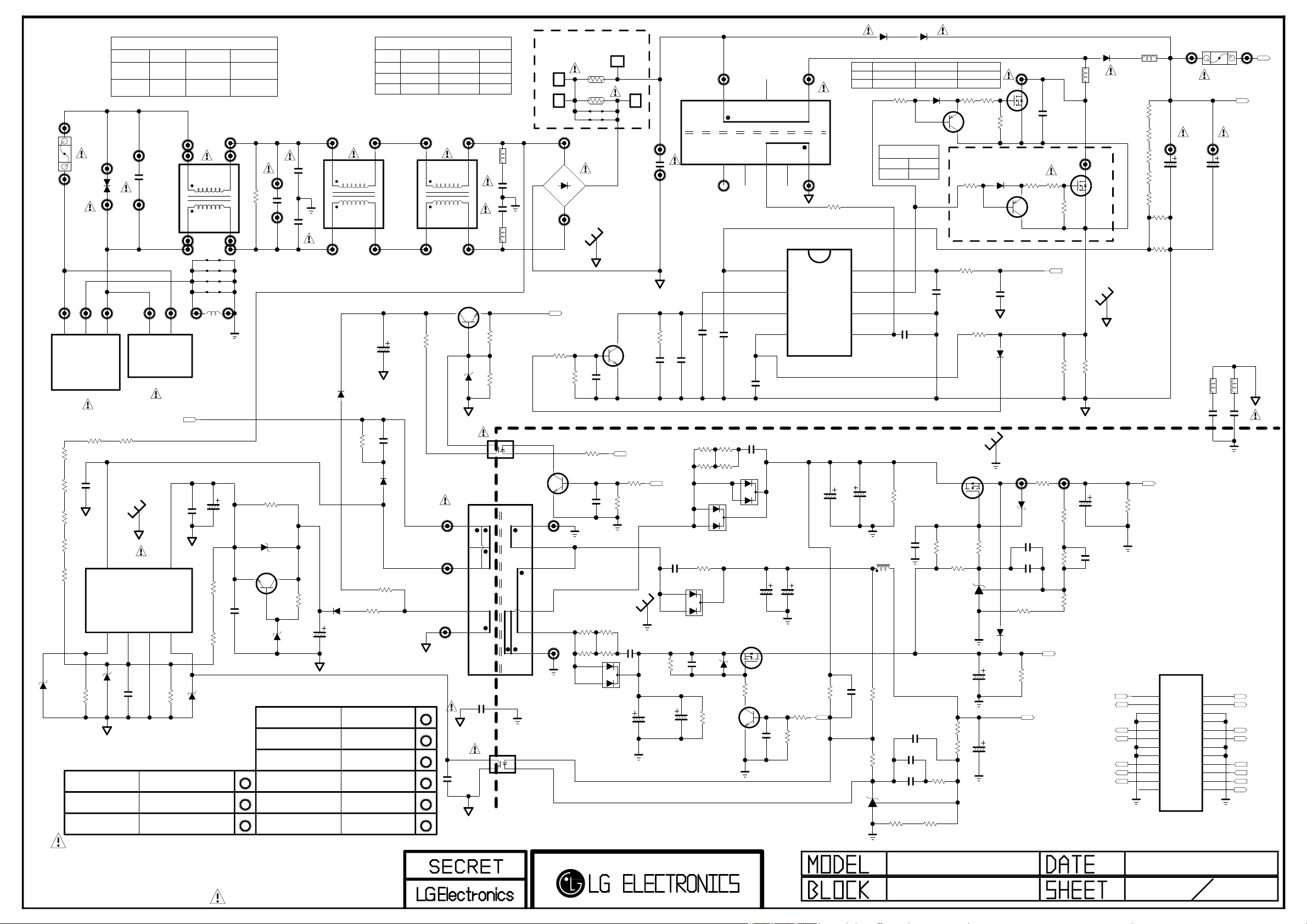
Schematic Diagram
Rev 2.1
PLHF-L923A/B/C (REV.2.1)
28
Date: 2011. 04. 28
Page 29
OPTION2
1
P603
1
P601
AC2
BD101
3
1
4
A
2
1
C
Q201
E
9
10
12
13
14
1
2
R619
N.C
2
BD101
32",37":RS405M
42":RS1005M
AC1
VCC
N.C
R618
B
C230
0.1uF
50V
R228
22
R204
22
F100
32": T3.15A H 250V
37",42":T5A H 250V
L
SK101
DAC-11PM1
1%
R517
750K
1%
R516
750K
1%
R515
750K
1%
R514
750K
R513
750K
1%
IC501
STR-W6053N
5.6V
ZD503
R503
LGP32-10LF LGD FHD
LGP32-10LH LGD HD
LGP32-10LS Sharp FHD 120Hz
VA100
INR14D621
E
R518
750K
1%
C503
N.C
S/OCP
ZD501
1W
0.43
LF102,103
N
1
D/ST
3
6.8V
LF101
R519
1/4W
72*25
BL
OPTION1
1
C513
0.1uF
50V
4
FB
6
820K
1%
12
12
ZD504
37’
LLF-101
17mH 9mH
LLF-103
LF101
OPTION1
SK102
16V
32’
LLF-100 LLF-102
7.7mH
LLF-103
30mH
CX101
0.22uF
275V
3
PFC_MULTI
1M
HS2
VCC
GND
5
7
C502
0.1uF
50V
R509
J103
J104
J105
J106
L101
N.C
N.C
C506
R507
R508
2.7M
2.2M
N.C
3 4
3 4
42’
LLF-104
23mH30mH
CY101
470pF
R1001M1/2W
C504
N.C
ZD505
Q503
E
N.C
N.C
R510
0
ZD506
CX102
B
N.C
275V
0.47uF
CY102
C
N.C
R511
470pF
LGP37-10LF LGD FHD
LGP37-10LA AUO FHD(HD)
LGP42-10LF LGD FHD
EL65
LGP42-10LA AUO FHD (HD)
EL66
LGP42-10LC CMO FHD
EL67
LGP42-10LS Sharp FHD
C509
2
1
D502
D504
UF4007
50V
10uF
LF102
OPTION1
UF4007
R501
32’ 5D-15
37’
42’
3
4
C510
22uF
50V
C501
1000pF
100K
2W
1KV
1KV
D501
UF4007
R512
1/2W
2.2
R504
22
1/2W
RD
OPTION2
TH600 TH601
N.C
N.C
2
1
R505
1K
EL68
EL69
EL70
EL71
EL72
EL73
5D-15
2.5D-152.5D-15
LF103
OPTION1
B+
D
C
ZD502
C505
4700pF
50V
J101,102
JUMPER
JUMPER
N.C
3
4
Q502
KTC3551T
E
B
R502
100K
16V
N.C
R506
3
3
4
4
T501
LPM-100
7 8
5
3
2
CY105
470pF
4
4
3
3
LB101LB102
CY103
470pF
CY104
470pF
R-TYPE R-TYPE
2
1
EL817MB-DT
IC503
MMBT2222A
IC502
EL817MB-DT
1
2
THE SYMBOL MARK OF THIS SCHEMETIC DIAGRAM INCORPORATES
SPECIAL FEATURES IMPORTANT FOR PROTECTION FROM X-RADIATION.
FILRE AND ELECTRICAL SHOCK HAZARDS, WHEN SERVICING IF IS
ESSENTIAL THAT ONLY MANUFATURES SPECFIED PARTS BE USED FOR
THE CRITICAL COMPONENTS IN THE SYMBOL MARK OF THE SCHEMETIC.
TH601
TH600
J101
J102
C
HS1
96*15
Q605
N.C
B
N.C
C609
R230
270
R232
R234
22
R233
22
A2
A1
D204
MBRF10200CT
12.5x20*2
P604
1
C
E
10K
C
C210
680uF
50V
1
0.82uF
3.5V
R231
470
HS5
28*12
C209
470pF
P602
C600
500V
R609
C601
0.1uF
50V
POWER-ON
1KV
10K
R222
C220
680uF
50V
C603
1000pF
50V
C602
0.047uF
50V
C203
470pF
1KV
D202
A2
A1
MBRF2060CT
47K
C216
2
11
R20122R229
22
R227
R226
22
22
D201
A2
C
A1
MBRF10150CT
R202
22
1W
C
1uF
50V
ZD201
51K
R205
10
C607
1000pF
50V
C604
100pF
50V
C201
470pF
1KV
D203
A2
C
A1
MBRF10150CT
C204
1000uF
10V
Q203
FDD5614P
S
N.C
G
R225
47K
C
Q204
MMBT2222A
E
C213
D600
1N5408
1KV
OPTION4
4
8
9
FB
1
CT
2
COMP
3
CS
4
C205
1000uF
10V
D
R223
50V
0.1uF
R224
470
POWER-ON
10K
B
67
IC600
HS01G
10x20*2
C219
N.C
R256
L600
32’,37’
LLP-100
42’
LLP-101
R608
20K
8
7
6
5
680uF
Q601
Q602
VCC
DRV
GND
ZCD
35V
C218
35V
680uF
L202
0.6uH
N.C
C214
R217
R218
4.7K
K
IC201
A
AZ431LANTR-1.24V
STF13NM60
37’, 42’ USING
330
R
D606
1N5408
1KV
32"
N.C
R604
200
OPTION3
32’ N.C
C605
R203
51K
C206
N.C
R221
430
1%
22pF
50V
C211
N.C
C232
N.C
C212
0.33uF
50V
37"
TK10A60
TK10A60
D604
1N4148W
B
Q604
MMBT2907A
C606
R207
10K
R219
3.3K
R220
820
1%
42"
STF13NM60
STF13NM60
R605
LB604
30
0
E
3216
R622
C
OPTION3
D603
R606
1N4148W
200
MMBT2907A
R614
2.2
0.1uF
50V
R615
3.3K
1%
D610
HS4
72*25
Q202
FQPF30N06L
D
S
G
R206
180
R212
2.2K
1%
K
R
IC202
A
AS431AN-2.5V
D205
C217
100uF
50V
1%
R215
1K
C215
470uF
1%
R216
1.2K
10V
REV 1.3
Q601
G
B
Q603
10K
C614
N.C
3216
N.C
ZD205
N.C
R214
18V
0.1uF
R211
180
1%
820
D
S
R620
E
C
C231
N.C
C207
50V
OPTION4
30
R235
0.05
5W
RS
2W
3.5V
1.9A
C608
220pF
1KV
LB602
0
3216
VCC
R621
R601
R208
300
R209
9.1K
R210
2.2K
20V
1.1A
Q602
G
10K
PCB P/N : EAX61124201
10L 32"37"42"NOR
PFC&MULTI
D601
STTH10LCD06FP
LB603
JUMPER
D
S
OPTION4
HS3
R601,R602
32",37":0.12
42":0.1
R602
2W
2W
C208
220uF
25V
1%
C221
1uF
1%
50V
1%
POWER-ON
20V
3.5V
3.5V
12V
12V
12V
LB601
R-TYPE
R610
750K
R611
750K
R612
750K
R613
750K
R616
750K
R617
240K
1%
R603
27K
1%
HS3
32":84*20
42",37":84*25
N.C
R213
FW20020-24SB
F501
1%
1%
1%
1%
1%
12V
2.8A
P201
1
3
5
7
9
11
13
15
17
19
21 22
23 24
F3.15A H 250V
C611
82uF
450V
KMF
2
4
6
8
10
12
14
16
18
20
C612
82uF
450V
C611,C612
32":68uF*2
37":82uF*2
42":82uF*2
LB104
CY107
PFC_MULTI
KMF
N.C
LB103
N.C
CY106
PFC_INV
R-TYPE
330pF
20V
20V
3.5V
3.5V
ON/OFF
A-DIM
P-DIM
ERROR
2010. 9. 13
1 3
Page 30
P-DIM
ERROR
ON/OFF
Module
LGD
AUO
SHARP
R303
1K
Inch
32HD
32FHD
37FHD
42FHD
37FHD
42FHD
32FHD
42FHD
42FHDCMO
R307
R344
R302
R301
R306
51K/J
27K/J
150K/J
39K/J
62K/J
150K/J
62K/J39K/J
150K/J
62K/J39K/J
150K/J
51K/J27K/J
150K/J
27K/J
51K/J
100K/J
27K/J
51K/J
200K/J
150K/J
27K/J N.C
51K/J
200K/J
R328
VR301
R324
22K
20K
R305
1K
50V
C324
0.1uF
150K
R328
N.C 10K
N.C
N.C
N.C
N.C
N.C
N.C
R301
R302
C304
1000pF
50V
R309
VR301
C302
0.01uF
R304
100K
10K
HS6
C720
N.C
C707
LB703
D
S
D
S
LB702
JUMPER
2SK3868
A-TYPE
2SK3868
72*20
C721
N.C
C706
Module
LGD
AUO
SHARP
CMO
LB704
R-TYPE
Inch
32HD
32FHD
37FHD
42FHD
37FHD
42FHD
32FHD
42FHD
42FHD
C719
0.82uF
N.C
C703
C716
N.C
C717
C706
100pF
100pF 100pF
100pF 100pF
100pF
500V
C718
100pF
100pF100pF
100pF100pF
100pF100pF
100pF
100pF100pF
100pF100pF
N.C
C707
32
N.C
1 4
UU1654
T703
32
1 4
UU1654
T704
Inch
T703,
Module
32HD
32FHD
LGD
37FHD
42FHD
37FHD
AUO
42FHD
32FHD
SHARP
42FHD
CMO
42FHD
Inch
Module R403 R406
32HD
32FHD
LGD
37FHD
42FHD
37FHD
AUO
42FHD
32FHD
SHARP
42FHD
42FHD
CMO
T704
LIH32-100L
LIF32-100L
LIF37-100L
LIF42-100L
LIF37-101A
LIF42-101A
LIF32-101S
LIF42-103S
LIF42-102C
20/F 20/F
20/F20/F
12/F 12/F
12/F12/F
12/F
12/F
12/F
12/F
12/F 12/F
12/F 12/F
12/F12/F
BAV99
C
A
BAV99
C
A
D403
D404
P401
(BLACK)
35002WR-02L(BK)
1
2
3
P402
35002WR-02L(P)
1
2
3
C401
C402
6KV
6KV
D401
AC
C404
50V
AC
C404RSC406C405
0.015uF
0.015uF
0.01uF
0.015uF
0.015uF
0.015uF
0.015uF
0.015uF
5600pF 5600pF
N.C
0.015uF 0.015uF
N.C
0.015uF 0.015uF
BAV99
D402
BAV99
C
A
C
A
0.015uF
0.015uF
0.015uF
0.015uF
2200pF5600pF4700pF0.056uF
5600pF
AC
R403122W
1%
AC
R406122W
RS
LGD
AUO
SHARP
1%
32HD
32FHD
37FHD
42FHD
37FHD
42FHD
32FHD
42FHD
42FHDCMO
C405
50V
C403
C406
C402Module Inch
C401
54pF
22pF
22pF
54pF
22pF
54pF
22pF
54pF
5pF
39pF
5pF 39pF
22pF
39pF
22pF 54pF
10pF 54pF
50V
50V
C403
0.047uF
0.047uF
0.047uF
0.047uF
0.047uF
0.068uF
0.068uF
0.056uF 0.027uF 6800pF 6800pF
PFC_INV
LB701
JUMPER
D701
1N4148W
R710
R341
0
C319
0.022uF
50V
270
D702
1N4148W
R712
270
100V
1N4148W
D302
100V
1N4148W
D303
R727
270
D704
1N4148W
R342
R343
R711
10K
R713
R726
270
D703
1N4148W
R725
10K
C320
68pF
50V
10K
C321
68pF
50V
10K
T701
LIP-001
C710
1uF
25V
R312
2.2
10K
10K
10K
10K
10K
10K
10KN.C27K/J 51K/J
10K
CT_SYNC_OUT
CT_SYNC_IN
50V
R306
C305
0.1uF
50V
50V
C303
0.1uF
PGND
HFN2
REF4V
DUTY
FAIL
LN2
GND
SRT
RT
STB
BD9270F-E2
1
2
3
4
5
6
7
8
9
10
11
12
A-DIM
IC301
R310
100K
R326
470K
C325
N.C
LN1
24
HFN1
23
VCC
22
COMP
21
COMPSD
20
STRK
19
1%
C307
C314
1000pF
C309
0.047uF
50V
50V
N.C
C310
0.01uF
R313
39K
50V
SS
18
FB
17
IS
16
VS
15
VREF
14
CP
13
1%
R316
110K
1%
R315
110K
1%
1%
75K
R31 8
68K
R31 7
C308
1uF
25V
R319
10
R314
C311
100K
C315
50V
4700pF
50V
1000pF
R311
2.2
50V
1000pF
C318
C312
0.1uF
C313
1uF
25V
C306
N.C
R327
12V
50V
R325
Module
LGD
AUO
SHARP
CMO 42FHD
C317
C711
1uF
25V
Q305
N.C
N.C
ZD301
E
N.C
C316
C
N.C
R347
25V
0.47uF
R323
N.C
VR302
R308
Inch
32HD
3.9K/F
32FHD
37FHD
42FHD
37FHD
42FHD
32FHD
42FHD
6.2K/F
1.5K/F
6.2K/F
18K/F
6.2K/F
10K/F
6.2K/F
13K/F
6.2K/F
6.8K/F
5.1K/F
10K/F
6.2K/F
10K/F 4.7K/F 10K/J6.2K/F 10K/J
7.5K/F 6.2K/F 10K/F 20K/J 12K/J
B
R322
Q306
N.C
R323R308
6.2K/F
6.2K/F
6.2K/F
6.8K/F
6.8K/F
6.8K/F
15K/F
12V
C
E
N.C
R334
R322
R325
8.2K/J
8.2K/J
8.2K/J
9.1K/J
4.7K/J
5.1K/J 4.7K/J
10K/J
B
1
4
1
4
C322
N.C
R327
10K/J
10K/J
10K/J
10K/J
5.1K/J
10K/J
T702
LIP-001
N.C
R335
N.C
R336
C323
N.C
8
7
6
5
8
7
6
5
OPTION:N.C
R340
0
10K
C712
1000pF
50V
R724
C715
N.C
10K
C713
1000pF
50V
Q707
G
Q710
G
C714
N.C
D
S
D
S
2SK3868
Q708
G
Q709
G
2SK3868
THE SYMBOL MARK OF THIS SCHEMETIC DIAGRAM INCORPORATES
SPECIAL FEATURES IMPORTANT FOR PROTECTION FROM X-RADIATION.
FILRE AND ELECTRICAL SHOCK HAZARDS, WHEN SERVICING IF IS
ESSENTIAL THAT ONLY MANUFATURES SPECFIED PARTS BE USED FOR
THE CRITICAL COMPONENTS IN THE SYMBOL MARK OF THE SCHEMETIC.
REV 1.3
PCB P/N : EAX61124201
10L 32"37"42"NOR
2010. 9. 13
2INVERTER
3
Page 31

F100-*1
0215 3.15MXK
R301-*1
27K
R302-*1
51K
R306-*1
200K
R308-*1
3.9K
R322-*1
5.1K
R323-*1
6.2K
R325-*1
8.2K
R327-*1
5.1K
C401-*1
5pF
6KV
C402-*1
39pF
6KV
C403-*1
0.056uF
50V
C404-*1
0.01uF
50V
C405-*1
5600pF
50V
C406-*1
2200pF
50V
LF101-*2
17mH
3 4
R306-*2
100K
R308-*2
R308-*3
1.5K
18K
R323-*2
R323-*3
15K
4.7K
R325-*3
R325-*2
5.1K
4.7K
R327-*2
4.7K
C403-*2
0.068uF
50V
C404-*2
4700pF
50V
C406-*2
5600pF
50V
R308-*4
13K
R325-*4
10K
C404-*3
5600pF
50V
12
R308-*5
6800
LF102-*1
30mH
3 4
L600-*1
LF103-*1
12
30mH
3 4
12
BD101-*1
RS405M
AC1
2
C
4
AC2
A
1
3
LLP-100
1
3
5 6
10
9
8
7
C611-*1
68uF
450V
C612-*1
68uF
450V
TH601-*1
5-ohm
DSD 5D-15 MSST
R601-*1
0.12
2W
5%
R602-*1
0.12
2W
5%
D
Q601-*1
G
TK10A60D
S
D
Q602-*1
G
TK10A60D
S
T703-*1
LIF32-100L
1 4
T704-*1
LIF32-100L
1 4
T703-*2
LIF32-100L
1 4
32
T704-*2
LIF32-100L
1 4
32
32
32
T703-*3
LIF32-101S
1 4
T704-*3
LIF32-101S
1 4
T703-*4
LIF37-100L
1 4
32
T704-*4
LIF37-100L
1 4
32
32
32
T703-*5
LIF37-101A
1 4
T704-*5
LIF37-101A
1 4
T703-*6
LIF42-101A
1 4
32
T704-*6
LIF42-101A
1 4
32
32
32
T703-*7
LIF42-103S
1 4
T704-*7
LIF42-103S
1 4
32
32
THE SYMBOL MARK OF THIS SCHEMETIC DIAGRAM INCORPORATES
SPECIAL FEATURES IMPORTANT FOR PROTECTION FROM X-RADIATION.
FILRE AND ELECTRICAL SHOCK HAZARDS, WHEN SERVICING IF IS
ESSENTIAL THAT ONLY MANUFATURES SPECFIED PARTS BE USED FOR
THE CRITICAL COMPONENTS IN THE SYMBOL MARK OF THE SCHEMETIC.
REV 1.3
PCB P/N : EAX61124201
10L 32"37"42"NOR 2010. 9. 13
Multi Option
3
3
Page 32

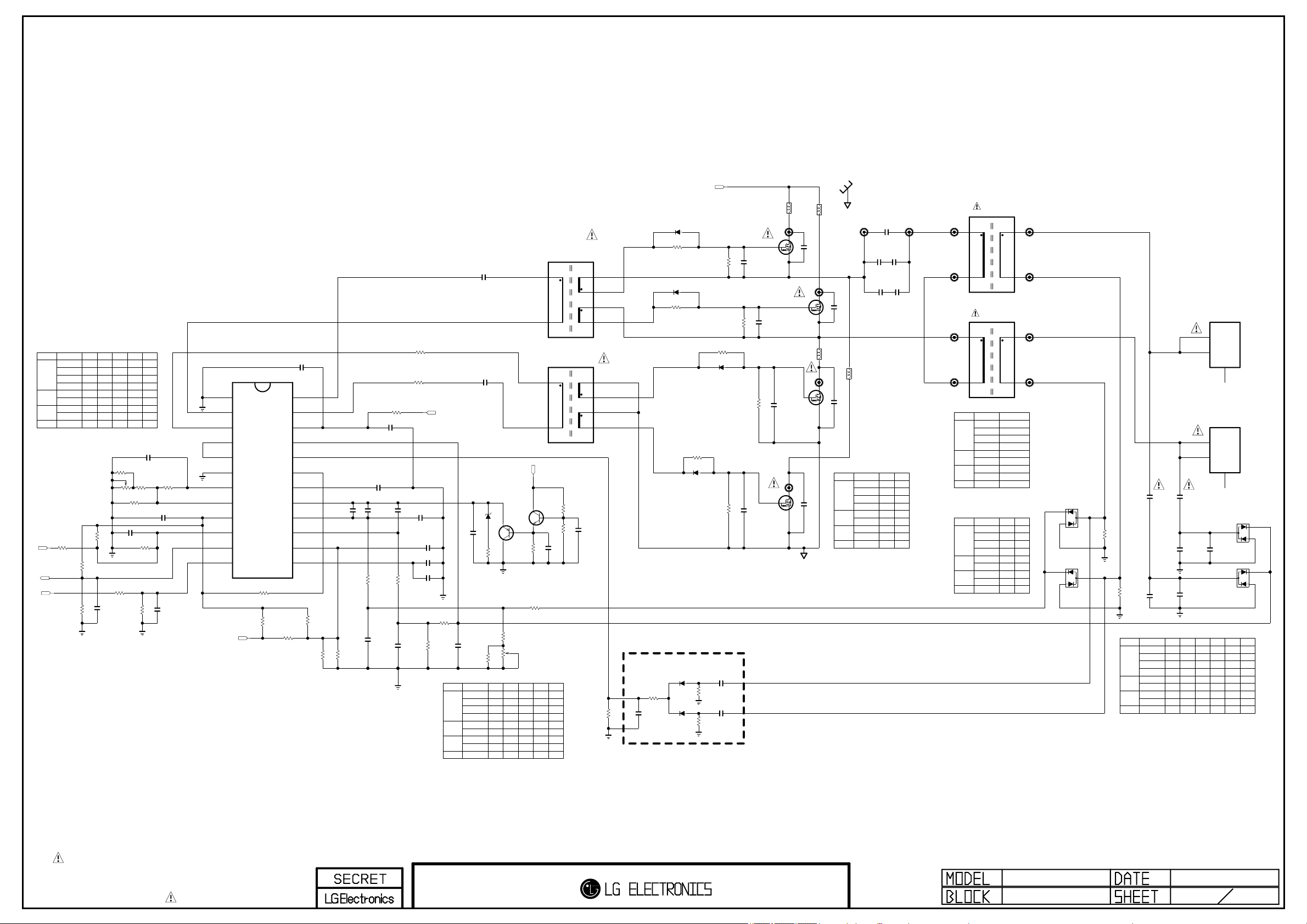
10L 42” LCD TV Power specification
Block Diagram
Rev 2.1
PLHF-L923A/B/C (REV.2.1)
29
Date: 2011. 04. 28
Page 33

10L 42” LCD TV Power specification
Rev 2.1
3.5V
MBRF2060
MBRF10150
12V
FQPF30N06L (Linear)
MBRF10200
20V
FDD5614P (Load S/W)
PWR On/Off
Inv. Lamp
Control IC
Inv. On/Off
- BD9270
■ Block Diagram
EE3370
EFD3634
(Flyback)
Multi Block
Control IC
STR-W6053N
Vcc
Inverter Block
UU1654
(F/Bridge)
2SK3868 x 4ea (N)
Control IC
- SCY99102
AC Input : 90~264V
PLHF-L923A/B/C (REV.2.1)
SQE x 1ea
EMI Filter
Common x 2ea
D10XB60
Bridge Diode
30
EER3618
PFC Block
450V 82uF x 2
Date: 2011. 04. 28
Page 34

10L 42” LCD TV Power specification
Rev 2.1
Parts List
PLHF-L923A/B/C (REV.2.1)
31
Date: 2011. 04. 28
Page 35

10L 42” LCD TV Power specification
No. LEVEL Q'TY Unit Location Specification Description Maker
1 1
2 g
EF-9301(g)
EC-19S-8
CS-9111LF-LGIT
FLUX
ALPHA METALS
동화다무라
청솔
2 1
0.018
㎏
HSE-11 B20 BAR(SN:99%, AG:0.3%, CU:0.7%) SOLDER BAR
서브원
HEESUNG METAL
3 1
0.0012
㎏
HSE-11 B20 WIRE(SN:99%, AG:0.3%, CU:0.7%) SOLDER W IRE
서브원
HEESUNG METAL
4 1
0.025
㎖
HT-130A-106 BOND-SMD HI-TECH KOREA
5 1
0.05
㎖
H-828W
OKE-410 (FOR AUTO DISPENSER)
TSE3854D
EA-4100
DS-818
SILICON
OKONG
OKONG
GE TOSHIBA
DOW CORNING
DONGYANG
6 1
1 Pcs BUBBLE SHEET (220W*720L 4+/- 1.5H) BUBBLE SHEET
서브원
JAEIL
A-TEK
7 1
1 Pcs LABEL FOR BOARD (40*8) LABEL
서브원
JAEIL
8 1
0.0625 Pcs LABEL FOR BOX LABEL-BOX
서브원
JAEIL
9 1
0.0031 Pcs TAPE 50*50K TAPE
서브원
JAEIL
10 1
0.0625 Pcs BOX(196W*246L*22H) BOX
서브원
JAEIL
HUAXING PACKING
TAILI PACKING
11 1
0.125 Pcs Tray Board (470*373) BOX_PAD
서브원
JAEIL
HUAXING PACKING
TAILI PACKING
12 1
0.1875 Pcs Cross Board A (472*250) PARTITION-A
서브원
JAEIL
HUAXING PACKING
TAILI PACKING
13 1
0.125 Pcs Cross Board B (375*250) PARTITION-B
서브원
JAEIL
HUAXING PACKING
TAILI PACKING
14
3 1 Pcs HEAT SINK Ass'y HEATSINK ASS'Y
15
4 1 Pcs HS1 HEAT SINK, 96*15*18.3(H) HEATSINK
YUWON NRT
HUAPENG
GUO TAI
16
4 1 Pcs BD101
DIODE BRIDGE D10XB60
DIODE BRIDGE RS1005M
DIODE BRIDGE TS10B05G
DIODE-BRIDGE
SHINDENGEN
RECTRON
TSC
17
4 1 Pcs FOR BD101
SEMS 3*12 SCREW,SPRING WASHER
BHM Screw, M3.0 *9.0L, with Clamfix, Cr3+WH Plating
SCREW
SEOUL METAL
ASEA BOLT
SUNGHO METAL
18
4 0.00001 kg FOR BD101 HC300 SILICON GLEASE
서브원
A-TEK
19
3 1 Pcs HEAT SINK Ass'y HEATSINK ASS'Y
20
4 1 Pcs HS2 HEAT SINK, 72*25*18.3(H) HEATSINK
YUWON NRT
HUAPENG
GUO TAI
21
4 1 Pcs IC501 STR-W6053N IC SANKEN
22
4 1 Pcs FOR IC501
SEMS 3*10 SCREW,SPRING WASHER
BHM Screw, M3.0 *8.0L, with Clamfix, Cr3+WH Plating
SCREW
SEOUL METAL
ASEA BOLT
SUNGHO METAL
23
4 0.00001 kg FOR IC501 HC300 SILICON GLEASE
서브원
A-TEK
24
3 1 Pcs HEAT SINK Ass'y HEATSINK ASS'Y
25
4 1 Pcs HS3 HEAT SINK, 84*25*18.3(H) HEATSINK
YUWON NRT
HUAPENG
GUO TAI
26
4 2 Pcs Q601 Q602
STF13NM60N
SD14N60
TK13A60D
FET
ST
INFINEON
TOSHIBA
27
4 1 Pcs D601
STTH10LCD06FP
BYV29FX-600
DIODE
ST
NXP
28
4 3 Pcs FOR Q601, Q602, D601
SEMS 3*10 SCREW,SPRING WASHER
BHM Screw, M3.0 *8.0L, with Clamfix, Cr3+WH Plating
SCREW
SEOUL METAL
ASEA BOLT
SUNGHO METAL
29
4 0.00003 kg FOR Q601, Q602, D601 HC300 SILICON GLEASE
서브원
A-TEK
30
3 1 Pcs HEAT SINK Ass'y HEATSINK ASS'Y
31
4 1 Pcs HS4 HEAT SINK, 72*25*18.3(H) HEATSINK
YUWON NRT
HUAPENG
GUO TAI
32
4 2 Pcs D201 D203
DIODE MBRF10150CT 10A 150V, TO-220FP
DIODE MBRF10U150CT 10A 150V, TO-220FP
DIODE FME-210B 10A 150V, TO-220FP
DIODE
SENSITRON
KEC
SANKEN
33
4 1 Pcs D204
DIODE MBRF10200CT 10A 200V, TO-220FP
DIODE MBRF10U200CT 10A 200V, TO-220FP
DIODE FMX-22S 10A 200V, TO-220FP
DIODE
SENSITRON
KEC
SANKEN
34
4 1 Pcs Q202
AP9972GI
FQPF30N06L
STP36NF06FP
TK30A06J3A
FET
APEC
FAIRCHILD
STM
TOSHIBA
Rev 2.1
LGP42-10LF(EAY60869402)
PLHF-L923A/B/C (REV.2.1)
32
Date: 2011. 04. 28
Page 36

10L 42” LCD TV Power specification
35
4 4 Pcs FOR D201, D203, D204, Q202
SEMS 3*10 SCREW,SPRING WASHER
BHM Screw, M3.0 *8.0L, with Clamfix, Cr3+WH Plating
SCREW
SEOUL METAL
ASEA BOLT
SUNGHO METAL
36
4 0.00004 kg FOR D201, D203, D204, Q202 HC300 SILICON GLEASE
서브원
A-TEK
37
3 1 Pcs HEAT SINK Ass'y HEATSINK ASS'Y
38
4 1 Pcs HS5 HEAT SINK, 20*11.5*28.75 HEATSINK
YUWON NRT
HUAPENG
GUO TAI
39
4 1 Pcs D202
DIODE MBRF2060CT 20A 60V, TO-220FP
DIODE MBRF2060CTL 20A 60V, TO-220FP
DIODE MBRF20U65CT 20A 65V, TO-220FP
DIODE FMW-2206 20A 60V, TO-220FP
DIODE
SENSITRON
SENSITRON
KEC
SANKEN
40
4 1 Pcs FOR D202
SEMS 3*10 SCREW,SPRING WASHER
BHM Screw, M3.0 *8.0L, with Clamfix, Cr3+WH Plating
SCREW
SEOUL METAL
ASEA BOLT
SUNGHO METAL
41
4 0.00001 kg FOR D202 HC300 SILICON GLEASE
서브원
A-TEK
42
3 1 Pcs HEAT SINK Ass'y HEATSINK ASS'Y
43
4 1 Pcs HS6 HEAT SINK, 72*20*18.3(H) HEAT SINK
YUWON NRT
HUAPENG
GUO TAI
44
4 4 Pcs Q707 Q708 Q709 Q710
2SK3868
FDPF5N50NZFT
KF5N50FS
FET
TOSHIBA
FAIRCHILD
KEC
45
4 4 Pcs FOR Q707 Q708 Q709 Q710
SEMS 3*10 SCREW,SPRING WASHER
BHM Screw, M3.0 *8.0L, with Clamfix, Cr3+WH Plating
SCREW
SEOUL METAL
ASEA BOLT
SUNGHO METAL
46
4 0.00004 kg FOR Q707 Q708 Q709 Q710 HC300 SILICON GLEASE
서브원
A-TEK
47
3 1 Pcs C401
EC 22pF J 6.3KV SL (10mm)
DM3JSL220J617 (10mm)
CC 3J SL 220J (10mm)
CC81 LY 22J (10mm)
High CAPACITOR
SAMWHA
APEX
동일전자
YINANDON
48
3 1 Pcs C402
EC 54pF J 6.3KV SL (10mm)
DM3JSL540J617 (10mm)
CC 3J SL 54J (10mm)
CC81 LY 54J (10mm)
High CAPACITOR
SAMWHA
APEX
동일전자
YINANDON
49
3 2 Pcs C600 C719
MPP 500V 824J 15F (15mm)
PCMP 372FL3824 500V 824J(15mm)
CAPACITOR-M/F
SUNGHO
PILKOR
50
3 2 Pcs C611 C612
KMF 450V 82uF LB(18x31.5mm)
SK 450V 82uF LR (18x32mm)
CAPACITOR-ELEC
SAMYOUNG
SUSCON
51
3 1 Pcs CX101
M.P.P PCX2 337 0.22uF K 100℃ AC275V P=15mm, SLIM-7T
CAPACITOR-X
PILKOR
OKAYA
Europtronic
52
3 1 Pcs CX102
M.P.P PCX2 337 0.47uF K 100℃ AC275V P=15mm, SLIM10T
CAPACITOR-X
PILKOR
OKAYA
Europtronic
53
3 5 Pcs CY101 CY102 CY103 CY104 CY105
SD B 2G 471K 08 BW, Y1, 105℃, P=10mm
DA2GYB471KK617(G), 105℃, P=10mm
DA2GYB471KBKC04, 105℃, P=10mm
CT81 471K 400V/AC, 105℃, P=10mm
CAPACITOR-Y
SAMWHA
APEX
동일전자
YINANDON
54
3 1 Pcs CY106
SD B 2G 331K 08 BW, Y1, 105℃, P=10mm
DA2GYB331KK617(G), 105℃, P=10mm
DA2GYB331KBKC04, 105℃, P=10mm
CT81 331K 400V/AC, 105℃, P=10mm
CAPACITOR-Y
SAMWHA
APEX
동일전자
YINANDON
55
3 2 Pcs D600 D606
S3V60 , 20mm
1N5408 , 20mm
1N5408 , 20mm
30PDA60, 20mm
DIODE
SHINDENGEN
RECTRON
TSC
NI
56
3 1 Pcs F100
T5A H 250V, 215, LEAD RED (1 LINE)
T5A H 250V, 50CT, LEAD RED (1 LINE)
FUSE
LITTEL FUSE
DAIN
57
3 1 Pcs F501
F3.15A H 250V, 216, LEAD VIOLET (2 LINE)
F3.15A H 250V, 50CF, LEAD VIOLET (2 LINE)
FUSE
LITTEL FUSE
DAIN
58
3 2 Pcs IC502 IC503
EL817M(DT) B TYPE(10mm)
LTV817M-BN TYPE(10mm)
PHOTO COUPLER
EVERLIGHT
LITEON
59
3 1 Pcs L202 LB-001,0.6uH(3*10), P6mm CHOKE-BAR
NAMYANG
CLOVER
SOOJUNG
LIENCHANG
60
3 1 Pcs L600 LLP-101 EER3618, 220uH PFC CHOKE
CLOVER
NAMYANG
SOOJUNG
KYOUNGIN
FEELUX
LIENCHANG
61
3 1 Pcs LF101 LLF-102, SQE2828 9mH LINE FILTER
CLOVER
NAMYANG
SOOJUNG
KYOUNGIN
FEELUX
LIENCHANG
62
3 2 Pcs LF102 LF103 LLF-104, CH935230 23mH LINE FILTER
CLOVER
SOOJUNG
KYOUNGIN
FEELUX
LIENCHANG
TNC
DONGIL TECH
63
3 1 Pcs P201
SMW200-24CF(B)
FW20020-24SB
CONNECTOR
YEONHO
FOOSUNG
64
3 1 Pcs P401 35002W R-02L(BK), Black, LOCKING TYPE CONNECTOR YEONHO
65
3 1 Pcs P402 35002W R-02L(P), White, LOCKING TYPE CONNECTOR YEONHO
Rev 2.1
PLHF-L923A/B/C (REV.2.1)
33
Date: 2011. 04. 28
Page 37

10L 42” LCD TV Power specification
66
3 3 Pcs PG102 PG103 PG104 Rug GND, SPCC 0.4t, CuSn Plating, 16.15L*7.4W*3.6H GROUND PLATE
ST TELECOM
LEZHI
SAMSUNG JS
DOSUNG
67
3 1 Pcs R235
MPR 5W 0.05 ohm J
MPR 5W 0.05 ohm J
RESISTOR-CEMENT
SMART
ABCO
68
3 1 Pcs SK101
DAC-11PM1
ST-A01-002LT
INLET
DONGIL TECH
BEJ
69
3 1 Pcs T501 LPM-100, EFD3634H, 1mH TRANSFORMER
CLOVER
NAMYANG
SOOJUNG
KYOUNGIN
FEELUX
LIENCHANG
70
3 2 Pcs T701 T702 LIP-001 TRANSFORMER
CLOVER
NAMYANG
SOOJUNG
KYOUNGIN
FEELUX
LIENCHANG
71
3 2 Pcs T703 T704 LIF42-100L, UU1654 TRANSFORMER
CLOVER
NAMYANG
KYOUNGIN
FEELUX
LIENCHANG
72
3 2 Pcs TH600 TH601
MF72-2.5D15
DSC2.5D15
THERMISTOR
NSE
DSC
73
3 1 Pcs VA100
INR14D621K(7.5mm),073C( BLACK TUBE)
SVC621D-14A,073C( BLACK TUBE)
VARISTOR
AMOTECH
SAMHWA
74
4 11 Pcs
C207 C213 C230 C303 C305 C312
C324 C502 C513 C601 C606
CAP FLAT 100NF K 50V X7R(2012) CAPACITOR-SMD
PILKOR
SAMSUNG
TDK
MURATA
TAIYOYUDEN
YAGEO
75
4 1 Pcs C212 CAP FLAT 0.33UF K 50V X7R 2012 CAPACITOR-SMD
PILKOR
SAMSUNG
TDK
MURATA
TAIYOYUDEN
YAGEO
76
4 1 Pcs C216 CAP FLAT 1UF K 50V X7R(2012) CAPACITOR-SMD
PILKOR
SAMSUNG
TDK
MURATA
TAIYOYUDEN
YAGEO
77
4 2 Pcs C302 C310 CAP FLAT 10NF K 50V X7R(2012) CAPACITOR-SMD
PILKOR
SAMSUNG
TDK
MURATA
TAIYOYUDEN
YAGEO
78
4 8 Pcs
C304 C314 C315 C318 C603 C607
C712 C713
CAP FLAT 1NF K 50V X7R(2012) CAPACITOR-SMD
PILKOR
SAMSUNG
TDK
MURATA
TAIYOYUDEN
YAGEO
79
4 5 Pcs C221 C308 C313 C710 C711 CAP FLAT 1UF K 25V X7R(2012) CAPACITOR-SMD
PILKOR
SAMSUNG
TDK
MURATA
TAIYOYUDEN
YAGEO
80
4 3 Pcs C309 C403 C602 CAP FLAT 47NF K 50V X7R(2012) CAPACITOR-SMD
PILKOR
SAMSUNG
TDK
MURATA
TAIYOYUDEN
YAGEO
81
4 2 Pcs C311 C505 CAP FLAT 4.7NF K 50V X7R(2012) CAPACITOR-SMD
PILKOR
SAMSUNG
TDK
MURATA
TAIYOYUDEN
YAGEO
82
4 1 Pcs C317 CAP FLAT 0.47UF K 25V X7R 2012 CAPACITOR-SMD
PILKOR
SAMSUNG
TDK
MURATA
TAIYOYUDEN
YAGEO
83
4 3 Pcs C404 C405 C406 CAP FLAT 15NF K 50V X7R(2012) CAPACITOR-SMD
PILKOR
SAMSUNG
TDK
MURATA
TAIYOYUDEN
YAGEO
Rev 2.1
PLHF-L923A/B/C (REV.2.1)
34
Date: 2011. 04. 28
Page 38

10L 42” LCD TV Power specification
84
4 1 Pcs C604 CAP FLAT 100PF J 50V CG(2012) CAPACITOR-SMD
PILKOR
SAMSUNG
TDK
MURATA
TAIYOYUDEN
YAGEO
85
4 1 Pcs C605 CAP FLAT 22PF J 50V CG(2012) CAPACITOR-SMD
PILKOR
SAMSUNG
TDK
MURATA
TAIYOYUDEN
YAGEO
86
4 4 Pcs D401 D402 D403 D404 BAV99 SOT-23 CHIP-DIODE
ON SEMI
NXP
DIODES
87
4 6 Pcs D603 D604 D701 D702 D703 D704
MMSD4148T, SOD-123
1N4148W, SOD-123
1N4148W, SOD-123
CHIP-DIODE
ON SEMI
DIODES
RECTRON
88
4 1 Pcs IC201
TLV431BSN1T1G, SOT-23, 1.24V±0.5%
AZ431LANTR-E1, SOT-23, 1.24V±0.5%
IC-SMD
ONSEMI
BCD
89
4 1 Pcs IC202
KIA431BM, SOT-23, 2.5V±0.5%
KA431SL, SOT-23, 2.5V±0.5%
AS431AN, SOT-23, 2.5V±0.5%
IC-SMD
KEC
FAIRCHILD
BCD
90
4 1 Pcs IC301 BD9270F, SOP-24 IC-SMD ROHM
91
4 1 Pcs IC600 SCY99102BDR2G, HS01G, SO-8 IC-SMD ONSEMI
92
4 2 Pcs LB602 LB604 RES FLAT 0J 1/4W(3216) RESISTOR-SMD
YAGEO
KAMAYA
PILKOR
SAMSUNG
ROHM
93
4 2 Pcs Q201 Q204
MMBT2222A , SOT-23
KTN2222AS, SOT-23
KST2222A , SOT-23
CHIP-TR
ONSEMI
KEC
FAIRCHILD
94
4 1 Pcs Q203
FDD5614P TO-252
NTD20P06L TO-252
FET-SMD
FAIRCHILD
ONSEMI
95
4 1 Pcs Q502
KTC3551, SOT-23
BCW66GL, SOT-23
CHIP-TR
KEC
ONSEMI
96
4 2 Pcs Q603 Q604
MMBT2907A, SOT-23
KTN2907AS, SOT-23
KST2907A, SOT-23
CHIP-TR
ONSEMI
KEC
FAIRCHILD
97
4 8 Pcs
R201 R204 R226 R227 R228 R229
R233 R234
RES FLAT 22 J 1/8W 2012 T&R RESISTOR-SMD
YAGEO
KAMAYA
PILKOR
SAMSUNG
ROHM
98
4 2 Pcs R203 R205 RES FLAT 51K J 1/8(2012) RESISTOR-SMD
YAGEO
KAMAYA
PILKOR
SAMSUNG
ROHM
99
4 1 Pcs R206 RES FLAT 180 J 1/8(2012) RESISTOR-SMD
YAGEO
KAMAYA
PILKOR
SAMSUNG
ROHM
100
4 12 Pcs
R207 R224 R232 R309 R327 R609
R621 R622 R711 R713 R724 R725
RES FLAT 10K J 1/8W 2012 RESISTOR-SMD
YAGEO
KAMAYA
PILKOR
SAMSUNG
ROHM
101
4 1 Pcs R208 RES FLAT 300 F 1/8(2012) RESISTOR-SMD
YAGEO
KAMAYA
PILKOR
SAMSUNG
ROHM
102
4 1 Pcs R209 RES FLAT 9.1K F 1/8W(2012) RESISTOR-SMD
YAGEO
KAMAYA
PILKOR
SAMSUNG
ROHM
103
4 2 Pcs R210 R212 RES FLAT, 2.2K, F, 1/8, 2012 RESISTOR-SMD
YAGEO
KAMAYA
PILKOR
SAMSUNG
ROHM
104
4 1 Pcs R211 RES FLAT 180 F 1/8W 2012 RESISTOR-SMD
YAGEO
KAMAYA
PILKOR
SAMSUNG
ROHM
105
4 1 Pcs R215 RES FLAT 1K F 1/8(2012) RESISTOR-SMD
YAGEO
KAMAYA
PILKOR
SAMSUNG
ROHM
106
4 1 Pcs R216 RES FLAT 1.2K F 1/8(2012) RESISTOR-SMD
YAGEO
KAMAYA
PILKOR
SAMSUNG
ROHM
107
4 1 Pcs R217 RES FLAT 330 J 1/8W(2012) RESISTOR-SMD
YAGEO
KAMAYA
PILKOR
SAMSUNG
ROHM
Rev 2.1
PLHF-L923A/B/C (REV.2.1)
35
Date: 2011. 04. 28
Page 39

10L 42” LCD TV Power specification
108
4 3 Pcs R303 R305 R505 RES FLAT 1K J 1/8(2012) RESISTOR-SMD
YAGEO
KAMAYA
PILKOR
SAMSUNG
ROHM
109
4 1 Pcs R219 RES FLAT 3.3K J 1/8(2012) RESISTOR-SMD
YAGEO
KAMAYA
PILKOR
SAMSUNG
ROHM
110
4 1 Pcs R220 RES FLAT 820 F 1/8(2012) RESISTOR-SMD
YAGEO
KAMAYA
PILKOR
SAMSUNG
ROHM
111
4 1 Pcs R221 RES FLAT 430 F 1/8W(2012) RESISTOR-SMD
YAGEO
KAMAYA
PILKOR
SAMSUNG
ROHM
112
4 1 Pcs R218 RES FLAT 4.7K J 1/8(2012) RESISTOR-SMD
YAGEO
KAMAYA
PILKOR
SAMSUNG
ROHM
113
4 2 Pcs R222 R225 RES FLAT 47K J 1/8(2012) RESISTOR-SMD
YAGEO
KAMAYA
PILKOR
SAMSUNG
ROHM
114
4 2 Pcs R223 R231 RES FLAT 470 J 1/8(2012) RESISTOR- SMD
YAGEO
KAMAYA
PILKOR
SAMSUNG
ROHM
115
4 5 Pcs R230 R710 R712 R726 R727 RES FLAT 270 J 1/8(2012) RESISTOR-SMD
YAGEO
KAMAYA
PILKOR
SAMSUNG
ROHM
116
4 1 Pcs R301 RES FLAT, 39K, F, 1/8, 2012 RESISTOR-SMD
YAGEO
KAMAYA
PILKOR
SAMSUNG
ROHM
117
4 1 Pcs R302 RES FLAT 62K F 1/8W 2012 RESISTOR-SMD
YAGEO
KAMAYA
PILKOR
SAMSUNG
ROHM
118
4 3 Pcs R304 R314 R502 RES FLAT 100K J 1/8W 2012 RESISTOR-SMD
YAGEO
KAMAYA
PILKOR
SAMSUNG
ROHM
119
4 2 Pcs R306 R344 RES FLAT 150K J 1/8(2012) RESISTOR-SMD
YAGEO
KAMAYA
PILKOR
SAMSUNG
ROHM
120
4 2 Pcs R307 R608 RES FLAT 20K J 1/8W 2012 T&R RESISTOR-SMD
YAGEO
KAMAYA
PILKOR
SAMSUNG
ROHM
121
4 1 Pcs R308 RES FLAT 10K F 1/8W 2012 RESISTOR-SMD
YAGEO
KAMAYA
PILKOR
SAMSUNG
ROHM
122
4 1 Pcs R310 RES FLAT 100K F 1/8(2012) RESISTOR-SMD
YAGEO
KAMAYA
PILKOR
SAMSUNG
ROHM
123
4 3 Pcs R311 R312 R614 RES FLAT 2.2 J 1/8 (2012) RESISTOR-SMD
YAGEO
KAMAYA
PILKOR
SAMSUNG
ROHM
124
4 1 Pcs R313 RES FLAT 39K J 1/8W 2012 RESISTOR-SMD
YAGEO
KAMAYA
PILKOR
SAMSUNG
ROHM
125
4 2 Pcs R315 R316 RES FLAT 110K F 1/8W 2012 RESISTOR-SMD
YAGEO
KAMAYA
PILKOR
SAMSUNG
ROHM
126
4 1 Pcs R317 RES FLAT 75K F 1/8(2012) RESISTOR-SMD
YAGEO
KAMAYA
PILKOR
SAMSUNG
ROHM
127
4 1 Pcs R318 RES FLAT 68K F 1/8W 2012 RESISTOR-SMD
YAGEO
KAMAYA
PILKOR
SAMSUNG
ROHM
Rev 2.1
PLHF-L923A/B/C (REV.2.1)
36
Date: 2011. 04. 28
Page 40

10L 42” LCD TV Power specification
128
4 1 Pcs R319 RES FLAT 10 J 1/8(2012) RESISTOR-SMD
YAGEO
KAMAYA
PILKOR
SAMSUNG
ROHM
129
4 1 Pcs R322 RES FLAT 6.2K F 1/8(2012) RESISTOR-SMD
YAGEO
KAMAYA
PILKOR
SAMSUNG
ROHM
130
4 1 Pcs R323 RES FLAT 6.8K F 1/8(2012) RESISTOR-SMD
YAGEO
KAMAYA
PILKOR
SAMSUNG
ROHM
131
4 1 Pcs R324 RES FLAT 22K J 1/8(2012) RESISTOR-SMD
YAGEO
KAMAYA
PILKOR
SAMSUNG
ROHM
132
4 1 Pcs R325 RES FLAT 9.1K J 1/8(2012) RESISTOR-SMD
YAGEO
KAMAYA
PILKOR
SAMSUNG
ROHM
133
4 1 Pcs R326 RES FLAT, 470K, F, 1/8, 2012 RESISTOR-SMD
YAGEO
KAMAYA
PILKOR
SAMSUNG
ROHM
134
4 2 Pcs R340 R510 RES FLAT 0 J 1/8(2012) RESISTOR-SMD
YAGEO
KAMAYA
PILKOR
SAMSUNG
ROHM
135
4 1 Pcs R507 RES FLAT 2.7M J 1/8W(2012) RESISTOR-SMD
YAGEO
KAMAYA
PILKOR
SAMSUNG
ROHM
136
4 1 Pcs R508 RES FLAT 2.2M F 1/8W 2012 RESISTOR-SMD
YAGEO
KAMAYA
PILKOR
SAMSUNG
ROHM
137
4 1 Pcs R509 RES FLAT 820K F 1/8W 2012 RESISTOR-SMD
YAGEO
KAMAYA
PILKOR
SAMSUNG
ROHM
138
4 11 Pcs
R513 R514 R515 R516 R517 R518
R610 R611 R612 R613 R616
RES FLAT 750K F 1/8W 2012 T&R RESISTOR-SMD
YAGEO
KAMAYA
PILKOR
SAMSUNG
ROHM
139
4 1 Pcs R603 RES FLAT 27K F 1/8 (2012) RESISTOR-SMD
YAGEO
KAMAYA
PILKOR
SAMSUNG
ROHM
140
4 2 Pcs R604 R606 RES FLAT 200 J 1/8W(2012) RESISTOR-SMD
YAGEO
KAMAYA
PILKOR
SAMSUNG
ROHM
141
4 2 Pcs R605 R620 RES FLAT 30 J 1/8(2012) RESISTOR-SMD
YAGEO
KAMAYA
PILKOR
SAMSUNG
ROHM
142
4 1 Pcs R615 RES FLAT 3.3K F 1/8(2012) RESISTOR-SMD
YAGEO
KAMAYA
PILKOR
SAMSUNG
ROHM
143
4 1 Pcs R617 RES FLAT 240K F 1/8 (2012) RESISTOR-SMD
YAGEO
KAMAYA
PILKOR
SAMSUNG
ROHM
144
4 1 Pcs ZD205
MM3Z18VST1G 18V, SOD323
MMSZ5248BS, 18V, SOD323
BZT52C18S,18V, SOD323
KDZ18V-RTK/P, SOD323
DIODE-ZENER-SMD
ON-SEMI
RECTRON
DIODES
KEC
145
4 1 Pcs ZD501
MM3Z6V8ST1G, SOD323
MMSZ5235BS, 6.8V, SOD323
BZT52C6V8S,6.8V, SOD323
KDZ 6.8V-RTK/P, SOD323
DIODE-ZENER-SMD
ON-SEMI
RECTRON
DIODES
KEC
Rev 2.1
PLHF-L923A/B/C (REV.2.1)
37
Date: 2011. 04. 28
Page 41

10L 42” LCD TV Power specification
146
5 3 Pc s C201 C203 C209
EK R 3A 471K 07 FK 5, 125℃, 1KV, P =5MM
DG3AHR471K959, 125℃, 1KV, P=5MM
CK3AYR471KFK, 125℃, 1KV, P= 5MM
CC81 1KV 471K 470PF, 125℃, 1KV, P=5MM
CAPACITOR-CER
SAMWHA
APEX
동일전자
YINANDON
147
5 2 Pc s C204 C205
NXB 1000uF 10V (10x16mm)
SG 1000uF 10V (10x16mm)
CAPACITOR-ELEC
SAMYOUNG
SUSCON
148
5 1 Pc s C208
NXB 220uF 25V (8x11.5mm)
SG 220uF 25V (8x12mm)
CAPACITOR-ELEC
SAMYOUNG
SUSCON
149
5 2 Pc s C210 C220
KMG 50V 680uF (12.5x20mm)
SK 50V 680uF (12.5x20mm)
CAPACITOR-ELEC
SAMYOUNG
SUSCON
150
5 1 Pc s C215
NXB 470UF 10V (8x11.5mm)
SG 470uF 10V (8x12mm)
CAPACITOR-ELEC
SAMYOUNG
SUSCON
151
5 1 Pc s C217
NXB 100uF 50V (8*11.5mm)
SG 100uF 50V (8x12mm)
CAPACITOR-ELEC
SAMYOUNG
SUSCON
152
5 2 Pc s C218 C219
NXB 35V 680M (10x20mm)
SG 35V 680M (10x20mm)
CAPACITOR-ELEC
SAMYOUNG
SUSCON
153
5 1 Pc s C501
EK R 3A 102K 09 FK 5, 125℃, 1KV, P =5MM
DG3AHR102K959, 125℃, 1KV, P=5MM
CK3AYR102KFK, 125℃, 1KV, P= 5MM
CC81 1KV 102K 1000PF, 125℃, 1KV, P=5MM
CAPACITOR-CER
SAMWHA
APEX
동일전자
YINANDON
154
5 1 Pc s C509
NXB 10uF 50V (5*11mm)
SG 10uF 50V (5x11mm)
CAPACITOR-ELEC
SAMYOUNG
SUSCON
155
5 1 Pc s C510
NXB 22uF 50V (5*11mm)
SG 22uF 50V (5x11mm)
CAPACITOR-ELEC
SAMYOUNG
SUSCON
156
5 1 Pc s C608
EK R 3A 221K 06 FK 5, 125℃, 1KV, P =5MM
DG3AHR221K959, 125℃, 1KV, P=5MM
CK3AYR221KFK, 125℃, 1KV, P= 5MM
CC81 1KV 221K 220PF, 125℃, 1KV, P=5MM
CAPACITOR-CER
SAMWHA
APEX
동일전자
YINANDON
157
5 2 Pc s C706 C707
EK R 3A 101K 06 FK 5, 125℃, 1KV, P =5MM
DG3AHR101K959, 125℃, 1KV, P=5MM
CK3AYR101KFK, 125℃, 1KV, P= 5MM
CC81 1KV 101K 100PF, 125℃, 1KV, P=5MM
CAPACITOR-CER
SAMWHA
APEX
동일전자
YINANDON
158
5 3 Pc s D501 D502 D504
DIODE FRD UF4007 1A 1000V 75ns DO-41 T& R
UF4007,DO-41
HER108G,DO-41
UF1007,DO_41
DIODE
TSC
Fairchild
RECTRON
Diodes
159
5 17 Pcs
EL1 EL10 EL11 EL12 EL13 EL15 EL17
EL37 EL4 EL40 EL5 EL51 EL52 EL6
EL7 EL8 EL9
EYE-LET DIA 2.3*.3.1L EYELET
DARIN
LEZHI
SAMSUNG JS
DOSUNG
160
5 36 Pcs
EL14 EL16 EL21 EL22 EL23 EL24
EL26 EL27 EL28 EL29 EL30 EL31
EL32 EL33 EL34 EL35 EL36 EL38
EL39 EL41 EL42 EL43 EL44 EL45
EL46 EL47 EL48 EL49 EL50 EL53
EL55 EL57 EL58 EL63 EL64 EL70
EYELET DIA 1.6*3.0 EYELET
DARIN
LEZHI
SAMSUNG JS
DOSUNG
161
5 6 Pc s EL18 EL19 EL20 EL25 EL54 EL56 GRIPER DIA 1.6*2.6L GRIPER
DARIN
LEZHI
SAMSUNG JS
DOSUNG
162
5 53 Pcs
J1 J10 J103 J104 J105 J106 J12 J13
J14 J15 J16 J17 J18 J19 J20 J21 J22
J23 J24 J25 J27 J28 J29 J3 J30 J31 J32
J33 J34 J35 J36 J37 J38 J4 J40 J41 J43
J44 J45 J46 J47 J48 J49 J5 J50 J51 J52
J6 J8 J9 LB603 LB701 LB702
LEAD WIRE DΦ=0.6mm ROLL TYPE(UNIT:Kg) JUMPER
Tianjin Hongyuan,
ST TELECOM
TPI
DM
TPC
ILKWANG
163
5 5 Pc s LB101 LB102 LB103 LB601 LB704
BFS3550R2F
SER3550050BA
BEAD
SAMWHA
SCC
164
5 1 Pc s LB703
BFS3550A0L
SEB3550050BA
BEAD
SAMHWA
SCC
165
5 4 Pc s P601 P602 P603 P604 PIN 5.5 * Φ2.3 (right angle in the edge) GT PIN
ST TELECOM
LEZHI
SAMSUNG JS
DOSUNG
166
5 1 Pc s R100
MSR37 1/2W 1M ohm J S urge
PRC 1M J 1/2W Surge
RESISTOR-S URGE
PILKOR
SMART
167
5 1 Pc s R202
MORS 1N 22 ohm J
RSD 1W 22 ohm J
PR01 1W 22R ohm J
RESISTOR-M /O
ABCO
SMART
PILKOR
168
5 1 Pc s R214
MORS 2W 820 ohm J TC, MINI
RSD 2W 820Ω J TA63
PR02 2W 820R ohm J
RESISTOR-M /O
ABCO
SMART
PILKOR
169
5 2 Pc s R403 R406
MORS 2W 12R ohm F TC
RSD 12Ω F 2W TA63
PR02 2W 12R ohm F
RESISTOR-M /O
ABCO
SMART
PILKOR
170
5 1 Pc s R501
MORS 2W 100K ohm J
RSD 2W 100KΩ J TA63
PR02 2W 100K ohm J
RESISTOR-M /O
ABCO
SMART
PILKOR
171
5 1 Pc s R503
WNPS 1N 0.43 ohm J
PRN 1W 0.43 ohm J
WWR 1N 0.43 ohm J
RESISTOR-W /W
ABCO
SMART
PILKOR
172
5 1 Pc s R504
CRS 1/2W 22R ohm J TC
RDM 22Ω J 1/2W
SFR25H 1/2W 22R ohm J
RESISTOR-M /O
ABCO
SMART
PILKOR
173
5 1 Pc s R512
CRS 1/2W 2.2R ohm J TC
RDM 2.2Ω J 1/2W
SFR25H 1/2W 2R2 ohm J
RESISTOR-M /O
ABCO
SMART
PILKOR
174
5 1 Pc s R519
CR 1/4W 1M ohm J TC
RD 1MΩ J 1/4W
SFR25 1/4W 1M ohm J
RESISTOR-M /O
ABCO
SMART
PILKOR
175
5 2 Pc s R601 R602
WNPS 2N 0.1 ohm J
PRN 2W 0.1 ohm J
WWR 2N 0.1ohm J
RESISTOR-W /W
ABCO
SMART
PILKOR
Rev 2.1
PLHF-L923A/B/C (REV.2.1)
38
Date: 2011. 04. 28
Page 42

10L 42” LCD TV Power specification
176
5 1 Pcs VR301
NVZ6TLTA 10㏀
RES VARIABLE EVM-AASA01B14 10K 1/10W
RESISTOR-VR
HOKURIKU
PANASONIC
177
5 2 Pcs ZD502 ZD504
1N5246B, 16V, DO-35
MTZJ16B, DO-34
1N5246, 16V, DO-35
DIODE-ZENER
VISHAY
ROHM
RECTRON
178
5 1 Pcs ZD503
1N5232B, 5.6V, DO-35
MTZJ5.6B, DO-34
1N5232, 5.6V, DO-35
DIODE-ZENER
VISHAY
ROHM
RECTRON
179 6
1 Pcs
LGP323742-10L, (196x246),FR-1 1oz 1.6t (REV 1.3)
[DS:DS-1108, KB: KB-3152, CC:CCP-6440(SM)]
PCB
HUIHO
HSIANG KUO
SAMHAN
DAEDUCK GDS
(TIANJIN DAEDUCK)
CHIN POON
WEIJUN
Rev 2.1
PLHF-L923A/B/C (REV.2.1)
39
Date: 2011. 04. 28
Page 43

10L 42” LCD TV Power specification
No. LEVEL Q'TY Unit Location Specification Description Maker
1 1
2 g
EF-9301(g)
EC-19S-8
CS-9111LF-LGIT
FLUX
ALPHA METALS
동화다무라
청솔
2 1
0.018
㎏
HSE-11 B20 BAR(SN:99%, AG:0.3%, CU:0.7%) SOLDER BAR
서브원
HEESUNG METAL
3 1
0.0012
㎏
HSE-11 B20 WIRE(SN:99%, AG:0.3%, CU:0.7%) SOLDER WIRE
서브원
HEESUNG METAL
4 1
0.025
㎖
HT-130A-106 BOND-SMD HI-TECH KOREA
5 1
0.05
㎖
H-828W
OKE-410 (FOR AUTO DISPENSER)
TSE3854D
EA-4100
DS-818
SILICON
OKONG
OKONG
GE TOSHIBA
DOW CORNING
DONGYANG
6 1
1 Pcs BUBBLE SHEET (220W*720L 4+/- 1.5H) BUBBLE SHEET
서브원
JAEIL
A-TEK
7 1
1 Pcs LABEL FOR BOARD (40*8) LABEL
서브원
JAEIL
8 1
0.0625 Pcs LABEL FOR BOX LABEL-BOX
서브원
JAEIL
9 1
0.0031 Pcs TAPE 50*50K TAPE
서브원
JAEIL
10 1
0.0625 Pcs BOX(196W*246L*22H) BOX
서브원
JAEIL
HUAXING PACKING
TAILI PACKING
11 1
0.125 Pcs Tray Board (470*373) BOX_PAD
서브원
JAEIL
HUAXING PACKING
TAILI PACKING
12 1
0.1875 Pcs Cross Board A (472*250) PARTITION-A
서브원
JAEIL
HUAXING PACKING
TAILI PACKING
13 1
0.125 Pcs Cross Board B (375*250) PARTITION-B
서브원
JAEIL
HUAXING PACKING
TAILI PACKING
14
3 1 Pcs HEAT SINK Ass'y HEATSINK ASS'Y
15
4 1 Pcs HS1 HEAT SINK, 96*15*18.3(H) HEATSINK
YUWON NRT
HUAPENG
GUO TAI
16
4 1 Pcs BD101
DIODE BRIDGE D10XB60
DIODE BRIDGE RS1005M
DIODE BRIDGE TS10B05G
DIODE-BRIDGE
SHINDENGEN
RECTRON
TSC
17
4 1 Pcs FOR BD101
SEMS 3*12 SCREW,SPRING WASHER
BHM Screw, M3.0 *9.0L, with Clamfix, Cr3+WH Plating
SCREW
SEOUL METAL
ASEA BOLT
SUNGHO METAL
18
4 0.00001 kg FOR BD101 HC300 SILICON GLEASE
서브원
A-TEK
19
3 1 Pcs HEAT SINK Ass'y HEATSINK ASS'Y
20
4 1 Pcs HS2 HEAT SINK, 72*25*18.3(H) HEATSINK
YUWON NRT
HUAPENG
GUO TAI
21
4 1 Pcs IC501 STR-W6053N IC SANKEN
22
4 1 Pcs FOR IC501
SEMS 3*10 SCREW,SPRING WASHER
BHM Screw, M3.0 *8.0L, with Clamfix, Cr3+WH Plating
SCREW
SEOUL METAL
ASEA BOLT
SUNGHO METAL
23
4 0.00001 kg FOR IC501 HC300 SILICON GLEASE
서브원
A-TEK
24
3 1 Pcs HEAT SINK Ass'y HEATSINK ASS'Y
25
4 1 Pcs HS3 HEAT SINK, 84*25*18.3(H) HEATSINK
YUWON NRT
HUAPENG
GUO TAI
26
4 2 Pcs Q601 Q602
STF13NM60N
SD14N60
TK13A60D
FET
ST
INFINEON
TOSHIBA
27
4 1 Pcs D601
STTH10LCD06FP
BYV29FX-600
DIODE
ST
NXP
28
4 3 Pcs FOR Q601, Q602, D601
SEMS 3*10 SCREW,SPRING WASHER
BHM Screw, M3.0 *8.0L, with Clamfix, Cr3+WH Plating
SCREW
SEOUL METAL
ASEA BOLT
SUNGHO METAL
29
4 0.00003 kg FOR Q601, Q602, D601 HC300 SILICON GLEASE
서브원
A-TEK
30
3 1 Pcs HEAT SINK Ass'y HEATSINK ASS'Y
31
4 1 Pcs HS4 HEAT SINK, 72*25*18.3(H) HEATSINK
YUWON NRT
HUAPENG
GUO TAI
32
4 2 Pcs D201 D203
DIODE MBRF10150CT 10A 150V, TO-220FP
DIODE MBRF10U150CT 10A 150V, TO-220FP
DIODE FME-210B 10A 150V, TO-220FP
DIODE
SENSITRON
KEC
SANKEN
33
4 1 Pcs D204
DIODE MBRF10200CT 10A 200V, TO-220FP
DIODE MBRF10U200CT 10A 200V, TO-220FP
DIODE FMX-22S 10A 200V, TO-220FP
DIODE
SENSITRON
KEC
SANKEN
Rev 2.1
LGP42-10LA(EAY60869403)
PLHF-L923A/B/C (REV.2.1)
40
Date: 2011. 04. 28
Page 44

10L 42” LCD TV Power specification
34
4 1 Pcs Q202
AP9972GI
FQPF30N06L
STP36NF06FP
TK30A06J3A
FET
APEC
FAIRCHILD
STM
TOSHIBA
35
4 4 Pcs FOR D201, D203, D204, Q202
SEMS 3*10 SCREW,SPRING WASHER
BHM Screw, M3.0 *8.0L, with Clamfix, Cr3+WH Plating
SCREW
SEOUL METAL
ASEA BOLT
SUNGHO METAL
36
4 0.00004 kg FOR D201, D203, D204, Q202 HC300 SILICON GLEASE
서브원
A-TEK
37
3 1 Pcs HEAT SINK Ass'y HEATSINK ASS'Y
38
4 1 Pcs HS5 HEAT SINK Extrued Al6063 20*11.5*28.75 HEATSINK
YUWON NRT
HUAPENG
GUO TAI
39
4 1 Pcs D202
DIODE MBRF2060CT 20A 60V, TO-220FP
DIODE MBRF2060CTL 20A 60V, TO-220FP
DIODE MBRF20U65CT 20A 65V, TO-220FP
DIODE FMW-2206 20A 60V, TO-220FP
DIODE
SENSITRON
SENSITRON
KEC
SANKEN
40
4 1 Pcs FOR D202
SEMS 3*10 SCREW,SPRING WASHER
BHM Screw, M3.0 *8.0L, with Clamfix, Cr3+WH Plating
SCREW
SEOUL METAL
ASEA BOLT
SUNGHO METAL
41
4 0.00001 kg FOR D202 HC300 SILICON GLEASE
서브원
A-TEK
42
3 1 Pcs HEAT SINK Ass'y HEATSINK ASS'Y
43
4 1 Pcs HS6 HEAT SINK, 72*20*18.3(H) HEATSINK
YUWON NRT
HUAPENG
GUO TAI
44
4 4 Pcs Q707 Q708 Q709 Q710
2SK3868
FDPF5N50NZFT
KF5N50FS
FET
TOSHIBA
FAIRCHILD
KEC
45
4 4 Pcs FOR Q707 Q708 Q709 Q710
SEMS 3*10 SCREW,SPRING WASHER
BHM Screw, M3.0 *8.0L, with Clamfix, Cr3+WH Plating
SCREW
SEOUL METAL
ASEA BOLT
SUNGHO METAL
46
4 0.00004 kg FOR Q707 Q708 Q709 Q710 HC300 SILICON GLEASE
서브원
A-TEK
47
3 1 Pcs C401
EC 5pF J 6.3KV SL (10mm)
DM3JSL050J617 (10mm)
CC 3J SL 050J (10mm)
CC81 LY 5D (10mm)
High CAPACITOR
SAMWHA
APEX
동일전자
YINANDON
48
3 1 Pcs C402
EC 39pF J 6.3KV SL (10mm)
DM3JSL390J617 (10mm)
CC 3J SL 39J (10mm)
CC81 LY 39J (10mm)
High CAPACITOR
SAMWHA
APEX
동일전자
YINANDON
49
3 2 Pcs C600 C719
MPP 500V 824J 15F (15mm)
PCMP 372FL3824 500V 824J(15mm)
CAPACITOR-M/F
SUNGHO
PILKOR
50
3 2 Pcs C611 C612
KMF 450V 82uF LB(18x31.5mm)
SK 450V 82uF LR (18x32mm)
CAPACITOR-ELEC
SAMYOUNG
SUSCON
51
3 1 Pcs CX101
M.P.P PCX2 337 0.22uF K 100℃ AC275V P=15mm
CAPACITOR-X PILKOR
52
3 1 Pcs CX102
M.P.P PCX2 337 0.47uF K 100℃ AC275V P=15mm
CAPACITOR-X PILKOR
53
3 5 Pcs CY101 CY102 CY103 CY104 CY105
SD B 2G 471K 08 BW,Y1, 105℃, P=10mm
DA2GYB471KK617(G), 105℃, P=10mm
DA2GYB471KBKC04, 105℃, P=10mm
CT81 471K 400V/AC, 105℃, P=10mm
CAPACITOR-Y
SAMWHA
APEX
동일전자
YINANDON
54
3 1 Pcs CY106
SD B 2G 331K 08 BW,Y1, 105℃, P=10mm
DA2GYB331KK617(G), 105℃, P=10mm
DA2GYB331KBKC04, 105℃, P=10mm
CT81 331K 400V/AC, 105℃, P=10mm
CAPACITOR-Y
SAMWHA
APEX
동일전자
YINANDON
55
3 2 Pcs D600 D606
S3V60 , 20mm
1N5408 , 20mm
1N5408 , 20mm
30PDA60, 20mm
DIODE
SHINDENGEN
RECTRON
TSC
NI
56
3 1 Pcs F100
T5A H 250V, 215, LEAD RED
T5A H 250V, 50CT, LEAD RED
FUSE
LITTEL FUSE
DAIN
57
3 1 Pcs F501
F3.15A H 250V, 216, LEAD VIOLET
F3.15A H 250V, 50CF, LEAD VIOLET
FUSE
LITTEL FUSE
DAIN
58
3 2 Pcs IC502 IC503
EL817M(DT) B TYPE(10mm)
LTV817M-BN TYPE(10mm)
PHOTO COUPLER
EVERLIGHT
LITEON
59
3 1 Pcs L202 LB-001,0.6uH(3*10), P6mm CHOKE-BAR
NAMYANG
CLOVER
SOOJUNG
LIENCHANG
60
3 1 Pcs L600 LLP-101 EER3618, 220uH PFC CHOKE
CLOVER
NAMYANG
SOOJUNG
KYOUNGIN
FEELUX
LIENCHANG
61
3 1 Pcs LF101 LLF-102, SQE2828 9mH LINE FILTER
CLOVER
NAMYANG
SOOJUNG
KYOUNGIN
FEELUX
LIENCHANG
62
3 2 Pcs LF102 LF103 LLF-104, CH935230 23mH LINE FILTER
CLOVER
SOOJUNG
KYOUNGIN
FEELUX
LIENCHANG
TNC
DONGIL TECH
Rev 2.1
PLHF-L923A/B/C (REV.2.1)
41
Date: 2011. 04. 28
Page 45

10L 42” LCD TV Power specification
63
3 1 Pcs P201
SMW200-24CF(B)
FW20020-24SB
CONNECTOR
YEONHO
FOOSUNG
64
3 1 Pcs P401 35002WR-02L(BK), Black, LOCKING TYPE CONNECTOR YEONHO
65
3 1 Pcs P402 35002WR-02L(P), White, LOCKING TYPE CONNECTOR YEONHO
66
3 3 Pcs PG102 PG103 PG104 Rug GND, SPCC 0.4t, CuSn Plating, 16.15L*7.4W*3.6H GROUND PLATE
ST TELECOM
LEZHI
SAMSUNG JS
DOSUNG
67
3 1 Pcs R235
MPR 5W 0.05 ohm J
MPR 5W 0.05 ohm J
RESISTOR-CEMENT
SMART
ABCO
68
3 1 Pcs SK101
DAC-11PM1
ST-A01-002LT
INLET
DONGIL TECH
BEJ
69
3 1 Pcs T501 LPM-100, EFD3634H, 1mH TRANSFORMER
CLOVER
NAMYANG
SOOJUNG
KYOUNGIN
FEELUX
LIENCHANG
70
3 2 Pcs T701 T702 LIP-001 TRANSFORMER
CLOVER
NAMYANG
SOOJUNG
KYOUNGIN
FEELUX
LIENCHANG
71
3 2 Pcs T703 T704 LIF42-101A, UU1654 TRANSFORMER
CLOVER
NAMYANG
KYOUNGIN
FEELUX
LIENCHANG
72
3 2 Pcs TH600 TH601
MF72-2.5D15
DSC2.5D15
THERMISTOR
NSE
DSC
73
3 1 Pcs VA100
INR14D621K(7.5mm),073C (BLACK TUBE)
SVC621D-14A,073C (BLACK TUBE)
VARISTOR
AMOTECH
SAMHWA
74
4 11 Pcs
C207 C213 C230 C303 C305 C312
C324 C502 C513 C601 C606
CAP FLAT 100NF K 50V X7R(2012) CAPACITOR-SMD
PILKOR
SAMSUNG
TDK
MURATA
TAIYOYUDEN
YAGEO
75
4 1 Pcs C212 CAP FLAT 0.33UF K 50V X7R 2012 CAPACITOR-SMD
PILKOR
SAMSUNG
TDK
MURATA
TAIYOYUDEN
YAGEO
76
4 1 Pcs C216 CAP FLAT 1UF K 50V X7R(2012) CAPACITOR-SMD
PILKOR
SAMSUNG
TDK
MURATA
TAIYOYUDEN
YAGEO
77
4 2 Pcs C302 C310 CAP FLAT 10NF K 50V X7R(2012) CAPACITOR-SMD
PILKOR
SAMSUNG
TDK
MURATA
TAIYOYUDEN
YAGEO
78
4 8 Pcs
C304 C314 C315 C318 C603 C607
C712 C713
CAP FLAT 1NF K 50V X7R(2012) CAPACITOR-SMD
PILKOR
SAMSUNG
TDK
MURATA
TAIYOYUDEN
YAGEO
79
4 5 Pcs C221 C308 C313 C710 C711 CAP FLAT 1UF K 25V X7R(2012) CAPACITOR-SMD
PILKOR
SAMSUNG
TDK
MURATA
TAIYOYUDEN
YAGEO
80
4 3 Pcs C309 C403 C602 CAP FLAT 47NF K 50V X7R(2012) CAPACITOR-SMD
PILKOR
SAMSUNG
TDK
MURATA
TAIYOYUDEN
YAGEO
81
4 2 Pcs C311 C505 CAP FLAT 4.7NF K 50V X7R(2012) CAPACITOR-SMD
PILKOR
SAMSUNG
TDK
MURATA
TAIYOYUDEN
YAGEO
Rev 2.1
PLHF-L923A/B/C (REV.2.1)
42
Date: 2011. 04. 28
Page 46

10L 42” LCD TV Power specification
82
4 1 Pcs C317 CAP FLAT 0.47UF K 25V X7R 2012 CAPACITOR-SMD
PILKOR
SAMSUNG
TDK
MURATA
TAIYOYUDEN
YAGEO
83
4 3 Pcs C404 C405 C406 CAP FLAT 5.6NF K 50V X7R 2012 T&R CAPACITOR-SMD
PILKOR
SAMSUNG
TDK
MURATA
TAIYOYUDEN
YAGEO
84
4 1 Pcs C604 CAP FLAT 100PF J 50V CG(2012) CAPACITOR-SMD
PILKOR
SAMSUNG
TDK
MURATA
TAIYOYUDEN
YAGEO
85
4 1 Pcs C605 CAP FLAT 22PF J 50V CG(2012) CAPACITOR-SMD
PILKOR
SAMSUNG
TDK
MURATA
TAIYOYUDEN
YAGEO
86
4 4 Pcs D401 D402 D403 D404 BAV99 SOT-23 CHIP-DIODE
ON SEMI
NXP
DIODES
87
4 6 Pcs D603 D604 D701 D702 D703 D704
MMSD4148T, SOD-123
1N4148W, SOD-123
1N4148W, SOD-123
CHIP-DIODE
ON SEMI
DIODES
RECTRON
88
4 1 Pcs IC201
TLV431BSN1T1G, SOT-23, 1.24V±0.5%
AZ431LANTR-E1, SOT-23, 1.24V±0.5%
IC-SMD
ONSEMI
BCD
89
4 1 Pcs IC202
KIA431BM, SOT-23, 2.5V±0.5%
KA431SL, SOT-23, 2.5V±0.5%
AS431AN, SOT-23, 2.5V±0.5%
IC-SMD
KEC
FAIRCHILD
BCD
90
4 1 Pcs IC301 BD9270F, SOP-24 IC-SMD ROHM
91
4 1 Pcs IC600 SCY99102BDR2G, HS01G, SO-8 IC-SMD ONSEMI
92
4 2 Pcs LB602 LB604 RES FLAT 0J 1/4W(3216) RESISTOR-SMD
YAGEO
KAMAYA
PILKOR
SAMSUNG
ROHM
93
4 2 Pcs Q201 Q204
MMBT2222A , SOT-23
KTN2222AS, SOT-23
KST2222A , SOT-23
CHIP-TR
ONSEMI
KEC
FAIRCHILD
94
4 1 Pcs Q203
FDD5614P TO-252
NTD20P06L TO-252
FET-SMD
FAIRCHILD
ONSEMI
95
4 1 Pcs Q502
KTC3551, SOT-23
BCW66GL, SOT-23
CHIP-TR
KEC
ONSEMI
96
4 2 Pcs Q603 Q604
MMBT2907A, SOT-23
KTN2907AS, SOT-23
KST2907A, SOT-23
CHIP-TR
ONSEMI
KEC
FAIRCHILD
97
4 8 Pcs
R201 R204 R226 R227 R228 R229
R233 R234
RES FLAT 22 J 1/8W 2012 T&R RESISTOR-SMD
YAGEO
KAMAYA
PILKOR
SAMSUNG
ROHM
98
4 2 Pcs R203 R205 RES FLAT 51K J 1/8(2012) RESISTOR-SMD
YAGEO
KAMAYA
PILKOR
SAMSUNG
ROHM
99
4 1 Pcs R206 RES FLAT 180 J 1/8(2012) RESISTOR-SMD
YAGEO
KAMAYA
PILKOR
SAMSUNG
ROHM
100
4 11 Pcs
R207 R224 R232 R309 R609 R621
R622 R711 R713 R724 R725
RES FLAT 10K J 1/8W 2012 RESISTOR-SMD
YAGEO
KAMAYA
PILKOR
SAMSUNG
ROHM
101
4 1 Pcs R208 RES FLAT 300 F 1/8(2012) RESISTOR-SMD
YAGEO
KAMAYA
PILKOR
SAMSUNG
ROHM
102
4 1 Pcs R209 RES FLAT 9.1K F 1/8W(2012) RESISTOR-SMD
YAGEO
KAMAYA
PILKOR
SAMSUNG
ROHM
Rev 2.1
PLHF-L923A/B/C (REV.2.1)
43
Date: 2011. 04. 28
Page 47

10L 42” LCD TV Power specification
103
4 2 Pcs R210 R212 RES FLAT, 2.2K, F, 1/8, 2012 RESISTOR-SMD
YAGEO
KAMAYA
PILKOR
SAMSUNG
ROHM
104
4 1 Pcs R211 RES FLAT 180 F 1/8W 2012 RESISTOR-SMD
YAGEO
KAMAYA
PILKOR
SAMSUNG
ROHM
105
4 1 Pcs R215 RES FLAT 1K F 1/8(2012) RESISTOR-SMD
YAGEO
KAMAYA
PILKOR
SAMSUNG
ROHM
106
4 1 Pcs R216 RES FLAT 1.2K F 1/8(2012) RESISTOR-SMD
YAGEO
KAMAYA
PILKOR
SAMSUNG
ROHM
107
4 1 Pcs R217 RES FLAT 330 J 1/8W(2012) RESISTOR-SMD
YAGEO
KAMAYA
PILKOR
SAMSUNG
ROHM
108
4 3 Pcs R303 R305 R505 RES FLAT 1K J 1/8(2012) RESISTOR-SMD
YAGEO
KAMAYA
PILKOR
SAMSUNG
ROHM
109
4 1 Pcs R219 RES FLAT 3.3K J 1/8(2012) RESISTOR-SMD
YAGEO
KAMAYA
PILKOR
SAMSUNG
ROHM
110
4 1 Pcs R220 RES FLAT 820 F 1/8(2012) RESISTOR-SMD
YAGEO
KAMAYA
PILKOR
SAMSUNG
ROHM
111
4 1 Pcs R221 RES FLAT 430 F 1/8W(2012) RESISTOR-SMD
YAGEO
KAMAYA
PILKOR
SAMSUNG
ROHM
112
4 2 Pcs R222 R225 RES FLAT 47K J 1/8(2012) RESISTOR-SMD
YAGEO
KAMAYA
PILKOR
SAMSUNG
ROHM
113
4 2 Pcs R223 R231 RES FLAT 470 J 1/8(2012) RESISTOR-SMD
YAGEO
KAMAYA
PILKOR
SAMSUNG
ROHM
114
4 5 Pcs R230 R710 R712 R726 R727 RES FLAT 270 J 1/8(2012) RESISTOR-SMD
YAGEO
KAMAYA
PILKOR
SAMSUNG
ROHM
115
4 2 Pcs R301 RES FLAT 27K J 1/8 (2012) RESISTOR-SMD
YAGEO
KAMAYA
PILKOR
SAMSUNG
ROHM
116
4 2 Pcs R603 RES FLAT 27K F 1/8 (2012) RESISTOR-SMD
YAGEO
KAMAYA
PILKOR
SAMSUNG
ROHM
117
4 1 Pcs R302 RES FLAT 51K J 1/8W 2012 RESISTOR-SMD
YAGEO
KAMAYA
PILKOR
SAMSUNG
ROHM
118
4 4 Pcs R304 R306 R314 R502 RES FLAT 100K J 1/8W 2012 RESISTOR-SMD
YAGEO
KAMAYA
PILKOR
SAMSUNG
ROHM
119
4 1 Pcs R344 RES FLAT 150K J 1/8(2012) RESISTOR-SMD
YAGEO
KAMAYA
PILKOR
SAMSUNG
ROHM
120
4 2 Pcs R307 R608 RES FLAT 20K J 1/8W 2012 T&R RESISTOR-SMD
YAGEO
KAMAYA
PILKOR
SAMSUNG
ROHM
121
4 2 Pcs R308 R323 RES FLAT 6.8K F 1/8(2012) RESISTOR-SMD
YAGEO
KAMAYA
PILKOR
SAMSUNG
ROHM
Rev 2.1
PLHF-L923A/B/C (REV.2.1)
44
Date: 2011. 04. 28
Page 48

10L 42” LCD TV Power specification
122
4 1 Pcs R322 RES FLAT 5.1K F 1/8(2012) RESISTOR-SMD
YAGEO
KAMAYA
PILKOR
SAMSUNG
ROHM
123
4 1 Pcs R310 RES FLAT 100K F 1/8(2012) RESISTOR-SMD
YAGEO
KAMAYA
PILKOR
SAMSUNG
ROHM
124
4 3 Pcs R311 R312 R614 RES FLAT 2.2 J 1/8 (2012) RESISTOR-SMD
YAGEO
KAMAYA
PILKOR
SAMSUNG
ROHM
125
4 1 Pcs R313 RES FLAT 39K J 1/8W 2012 RESISTOR-SMD
YAGEO
KAMAYA
PILKOR
SAMSUNG
ROHM
126
4 2 Pcs R315 R316 RES FLAT 110K F 1/8W 2012 RESISTOR-SMD
YAGEO
KAMAYA
PILKOR
SAMSUNG
ROHM
127
4 1 Pcs R317 RES FLAT 75K F 1/8(2012) RESISTOR-SMD
YAGEO
KAMAYA
PILKOR
SAMSUNG
ROHM
128
4 1 Pcs R318 RES FLAT 68K F 1/8W 2012 RESISTOR-SMD
YAGEO
KAMAYA
PILKOR
SAMSUNG
ROHM
129
4 1 Pcs R319 RES FLAT 10 J 1/8(2012) RESISTOR-SMD
YAGEO
KAMAYA
PILKOR
SAMSUNG
ROHM
130
4 1 Pcs R324 RES FLAT 22K J 1/8(2012) RESISTOR-SMD
YAGEO
KAMAYA
PILKOR
SAMSUNG
ROHM
131
4 2 Pcs R218 R327 RES FLAT 4.7K J 1/8(2012) RESISTOR-SMD
YAGEO
KAMAYA
PILKOR
SAMSUNG
ROHM
132
4 1 Pcs R325 RES FLAT 5.1K J 1/8W 2012 RESISTOR-SMD
YAGEO
KAMAYA
PILKOR
SAMSUNG
ROHM
133
4 1 Pcs R326 RES FLAT, 470K, F, 1/8, 2012 RESISTOR-SMD
YAGEO
KAMAYA
PILKOR
SAMSUNG
ROHM
134
4 2 Pcs R340 R510 RES FLAT 0 J 1/8(2012) RESISTOR-SMD
YAGEO
KAMAYA
PILKOR
SAMSUNG
ROHM
135
4 1 Pcs R507 RES FLAT 2.7M J 1/8W(2012) RESISTOR-SMD
YAGEO
KAMAYA
PILKOR
SAMSUNG
ROHM
136
4 1 Pcs R508 RES FLAT 2.2M F 1/8W 2012 RESISTOR-SMD
YAGEO
KAMAYA
PILKOR
SAMSUNG
ROHM
137
4 1 Pcs R509 RES FLAT 820K F 1/8W 2012 RESISTOR-SMD
YAGEO
KAMAYA
PILKOR
SAMSUNG
ROHM
Rev 2.1
PLHF-L923A/B/C (REV.2.1)
45
Date: 2011. 04. 28
Page 49

10L 42” LCD TV Power specification
138
4 11 Pcs
R513 R514 R515 R516 R517 R518
R610 R611 R612 R613 R616
RES FLAT 750K F 1/8W 2012 T&R RESISTOR-SMD
YAGEO
KAMAYA
PILKOR
SAMSUNG
ROHM
139
4 2 Pcs R604 R606 RES FLAT 200 J 1/8W(2012) RESISTOR-SMD
YAGEO
KAMAYA
PILKOR
SAMSUNG
ROHM
140
4 2 Pcs R605 R620 RES FLAT 30 J 1/8(2012) RESISTOR-SMD
YAGEO
KAMAYA
PILKOR
SAMSUNG
ROHM
141
4 1 Pcs R615 RES FLAT 3.3K F 1/8(2012) RESISTOR-SMD
YAGEO
KAMAYA
PILKOR
SAMSUNG
ROHM
142
4 1 Pcs R617 RES FLAT 240K F 1/8 (2012) RESISTOR-SMD
YAGEO
KAMAYA
PILKOR
SAMSUNG
ROHM
143
4 1 Pcs ZD205
MM3Z18VST1G 18V, SOD323
MMSZ5248BS, 18V, SOD323
BZT52C18S,18V, SOD323
KDZ18V-RTK/P, SOD323
DIODE-ZENER-SMD
ON-SEMI
RECTRON
DIODES
KEC
144
4 1 Pcs ZD501
MM3Z6V8ST1G, SOD323
MMSZ5235BS, 6.8V, SOD323
BZT52C6V8S,6.8V, SOD323
KDZ 6.8V-RTK/P, SOD323
DIODE-ZENER-SMD
ON-SEMI
RECTRON
DIODES
KEC
145
5 3 Pcs C201 C203 C209
EK R 3A 471K 07 FK5, 125℃, 1KV, P=5MM
DG3AHR471K959, 125℃, 1KV, P=5MM
CK3AYR471KFK, 125℃, 1KV, P=5MM
CC81 1KV 471K 470PF, 125℃, 1KV, P=5MM
CAPACITOR-CER
SAMWHA
APEX
동일전자
YINANDON
146
5 2 Pcs C204 C205
NXB 1000uF 10V (10x16mm)
SG 1000uF 10V (10x16mm)
CAPACITOR-ELEC
SAMYOUNG
SUSCON
147
5 1 Pcs C208
NXB 220uF 25V (8x11.5mm)
SG 220uF 25V (8x12mm)
CAPACITOR-ELEC
SAMYOUNG
SUSCON
148
5 2 Pcs C210 C220
KMG 50V 680uF (12.5x20mm)
SK 50V 680uF (12.5x20mm)
CAPACITOR-ELEC
SAMYOUNG
SUSCON
149
5 1 Pcs C215
NXB 470UF 10V (8x11.5mm)
SG 470uF 10V (8x12mm)
CAPACITOR-ELEC
SAMYOUNG
SUSCON
150
5 1 Pcs C217
NXB 100uF 50V (8*11.5mm)
SG 100uF 50V (8x12mm)
CAPACITOR-ELEC
SAMYOUNG
SUSCON
151
5 2 Pcs C218 C219
NXB 35V 680M (10x20mm)
SG 35V 680M (10x20mm)
CAPACITOR-ELEC
SAMYOUNG
SUSCON
152
5 1 Pcs C501
EK R 3A 102K 09 FK5, 125℃, 1KV, P=5MM
DG3AHR102K959, 125℃, 1KV, P=5MM
CK3AYR102KFK, 125℃, 1KV, P=5MM
CC81 1KV 102K 1000PF, 125℃, 1KV, P=5MM
CAPACITOR-CER
SAMWHA
APEX
동일전자
YINANDON
153
5 1 Pcs C509
NXB 10uF 50V (5*11mm)
SG 10uF 50V (5x11mm)
CAPACITOR-ELEC
SAMYOUNG
SUSCON
154
5 1 Pcs C510
NXB 22uF 50V (5*11mm)
SG 22uF 50V (5x11mm)
CAPACITOR-ELEC
SAMYOUNG
SUSCON
155
5 1 Pcs C608
EK R 3A 221K 06 FK5, 125℃, 1KV, P=5MM
DG3AHR221K959, 125℃, 1KV, P=5MM
CK3AYR221KFK, 125℃, 1KV, P=5MM
CC81 1KV 221K 220PF, 125℃, 1KV, P=5MM
CAPACITOR-CER
SAMWHA
APEX
동일전자
YINANDON
156
5 2 Pcs C706 C707
EK R 3A 101K 06 FK5, 125℃, 1KV, P=5MM
DG3AHR101K959, 125℃, 1KV, P=5MM
CK3AYR101KFK, 125℃, 1KV, P=5MM
CC81 1KV 101K 100PF, 125℃, 1KV, P=5MM
CAPACITOR-CER
SAMWHA
APEX
동일전자
YINANDON
157
5 3 Pcs D501 D502 D504
DIODE FRD UF4007 1A 1000V 75ns DO-41 T&R
UF4007,DO-41
HER108G,DO-41
UF1007,DO_41
DIODE
TSC
Fairchild
RECTRON
Diodes
158
5 17 Pcs
EL1 EL10 EL11 EL12 EL13 EL15
EL17 EL37 EL4 EL40 EL5 EL51 EL52
EL6 EL7 EL8 EL9
EYE-LET DIA 2.3*.3.1L EYELET
DARIN
LEZHI
SAMSUNG JS
DOSUNG
159
5 36 Pcs
EL14 EL16 EL21 EL22 EL23 EL24
EL26 EL27 EL28 EL29 EL30 EL31
EL32 EL33 EL34 EL35 EL36 EL38
EL39 EL41 EL42 EL43 EL44 EL45
EL46 EL47 EL48 EL49 EL50 EL53
EL55 EL57 EL58 EL63 EL64 EL71
EYELET DIA 1.6*3.0 EYELET
DARIN
LEZHI
SAMSUNG JS
DOSUNG
160
5 6 Pcs EL18 EL19 EL20 EL25 EL54 EL56 GRIPER DIA 1.6*2.6L GRIPER
DARIN
LEZHI
SAMSUNG JS
DOSUNG
Rev 2.1
PLHF-L923A/B/C (REV.2.1)
46
Date: 2011. 04. 28
Page 50

10L 42” LCD TV Power specification
161
5 53 Pcs
J1 J10 J103 J104 J105 J106 J12 J13
J14 J15 J16 J17 J18 J19 J20 J21 J22
J23 J24 J25 J27 J28 J29 J3 J30 J31 J32
J33 J34 J35 J36 J37 J38 J4 J40 J41 J43
J44 J45 J46 J47 J48 J49 J5 J50 J51 J52
J6 J8 J9 LB603 LB701 LB702
LEAD WIRE DΦ=0.6mm ROLL TYPE(UNIT:Kg) JUMPER
Tianjin Hongyuan,
ST TELECOM
TPI
DM
TPC
ILKWANG
162
5 5 Pcs LB101 LB102 LB103 LB601 LB704
BFS3550R2F
SER3550050BA
BEAD
SAMWHA
SCC
163
5 1 Pcs LB703
BFS3550A0L
SEB3550050BA
BEAD
SAMHWA
SCC
164
5 4 Pcs P601 P602 P603 P604 PIN 5.5 * Φ2. 3 (right angle in the edge) GT PIN
ST TELECOM
LEZHI
SAMSUNG JS
DOSUNG
165
5 1 Pcs R100
MSR37 1/2W 1M ohm J S urge
PRC 1M J 1/2W Surge
RESISTOR-SURGE
PILKOR
SMART
166
5 1 Pcs R202
MORS 1N 22 ohm J
RSD 1W 22 ohm J
PR01 1W 22R ohm J
RESISTOR-M/O
ABCO
SMART
PILKOR
167
5 1 Pcs R214
MORS 2W 820 ohm J TC, MINI
RSD 2W 820Ω J TA63
PR02 2W 820R ohm J
RESISTOR-M/O
ABCO
SMART
PILKOR
168
5 2 Pcs R403 R406
MORS 2W 12R ohm F TC
RSD 12Ω F 2W TA63
PR02 2W 12R ohm F
RESISTOR-M/O
ABCO
SMART
PILKOR
169
5 1 Pcs R501
MORS 2W 100K ohm J
RSD 2W 100KΩ J TA63
PR02 2W 100K ohm J
RESISTOR-M/O
ABCO
SMART
PILKOR
170
5 1 Pcs R503
WNPS 1N 0.43 ohm J
PRN 1W 0.43 ohm J
WWR 1N 0.43 ohm J
RESISTOR-W/W
ABCO
SMART
PILKOR
171
5 1 Pcs R504
CRS 1/2W 22R ohm J TC
RDM 22Ω J 1/2W
SFR25H 1/2W 22R ohm J
RESISTOR-M/O
ABCO
SMART
PILKOR
172
5 1 Pcs R512
CRS 1/2W 2.2R ohm J TC
RDM 2.2Ω J 1/2W
SFR25H 1/2W 2R2 ohm J
RESISTOR-M/O
ABCO
SMART
PILKOR
173
5 1 Pcs R519
CR 1/4W 1M ohm J TC
RD 1MΩ J 1/4W
SFR25 1/4W 1M ohm J
RESISTOR-M/O
ABCO
SMART
PILKOR
174
5 2 Pcs R601 R602
WNPS 2N 0.1 ohm J
PRN 2W 0.1 ohm J
WWR 2N 0.1ohm J
RESISTOR-W/W
ABCO
SMART
PILKOR
175
5 1 Pcs VR301
NVZ6TLTA 10㏀
RES VARIABLE E VM-AASA 01B14 10K 1/10W
RESISTOR-VR
HOKURIK U
PANASONIC
176
5 2 Pcs ZD502 ZD504
1N5246B, 16V, DO-35
MTZJ16B, DO-34
1N5246, 16V, DO-35
DIODE-ZENER
VISHAY
ROHM
RECTRON
177
5 1 Pcs ZD503
1N5232B, 5.6V, DO-35
MTZJ5.6B, DO-34
1N5232, 5.6V, DO-35
DIODE-ZENER
VISHAY
ROHM
RECTRON
178 6
1 Pcs
LGP323742-10L, (196x246),FR-1 1oz 1.6t (REV 1.3)
[DS:DS-1108, KB: KB-3152, CC:CCP-6440(SM)]
PCB
HUIHO
HSIANG KUO
SAMHAN
DAEDUCK GDS
(TIANJIN DAEDUCK)
CHIN POON
WEIJUN
Rev 2.1
PLHF-L923A/B/C (REV.2.1)
47
Date: 2011. 04. 28
Page 51

10L 42” LCD TV Power specification
No. LEVEL Q'TY Unit Location Specification Description Maker
1 1
2 g
EF-9301(g)
EC-19S-8
CS-9111LF-LGIT
FLUX
ALPHA METALS
동화다무라
청솔
2 1
0.018
㎏
HSE-11 B20 BAR(SN:99.7%, AG:0.3%, CU:0.7%) SOLDER BAR
서브원
HEESUNG METAL
3 1
0.0012
㎏
HSE-11 B20 WIRE(SN:99%, AG:0.3%, CU:0.7%) SOLDER WIRE
서브원
HEESUNG METAL
4 1
0.025
㎖
HT-130A-106 BOND-SMD HI-TECH KOREA
5 1
0.05
㎖
H-828W
OKE-410 (FOR AUTO DISPENSER)
TSE3854D
EA-4100
DS-818
SILICON
OKONG
OKONG
GE TOSHIBA
DOW CORNING
DONGYANG
6 1
1 Pcs BUBBLE SHEET (220W*720L 4+/- 1.5H) BUBBLE SHEET
서브원
JAEIL
A-TEK
7 1
1 Pcs LABEL FOR BOARD (40*8) LABEL
서브원
JAEIL
8 1
0.0625 Pcs LABEL FOR BOX LABEL-BOX
서브원
JAEIL
9 1
0.0031 Pcs TAPE 50*50K TAPE
서브원
JAEIL
10 1
0.0625 Pcs BOX(196W*246L*22H) BOX
서브원
JAEIL
HUAXING PACKING
TAILI PACKING
11 1
0.125 Pcs Tray Board (470*373) BOX_PAD
서브원
JAEIL
HUAXING PACKING
TAILI PACKING
12 1
0.1875 Pcs Cross Board A (472*250) PARTITION-A
서브원
JAEIL
HUAXING PACKING
TAILI PACKING
13 1
0.125 Pcs Cross Board B (375*250) PARTITION-B
서브원
JAEIL
HUAXING PACKING
TAILI PACKING
14
3 1 Pcs HEAT SINK Ass'y HEATSINK ASS'Y
15
4 1 Pcs HS1 HEAT SINK, 96*15*18.3(H) HEATSINK
YUWON NRT
HUAPENG
GUO TAI
16
4 1 Pcs BD101
DIODE BRIDGE D10XB60
DIODE BRIDGE RS1005M
DIODE BRIDGE TS10B05G
DIODE-BRIDGE
SHINDENGEN
RECTRON
TSC
17
4 1 Pcs FOR BD101
SEMS 3*12 SCREW,SPRING WASHER
BHM Screw, M3.0 *9.0L, with Clamfix, Cr3+WH Plating
SCREW
SEOUL METAL
ASEA BOLT
SUNGHO METAL
18
4 0.00001 kg FOR BD101 HC300 SILICON GLEASE
서브원
A-TEK
19
3 1 Pcs HEAT SINK Ass'y HEATSINK ASS'Y
20
4 1 Pcs HS2 HEAT SINK, 72*25*18.3(H) HEATSINK
YUWON NRT
HUAPENG
GUO TAI
21
4 1 Pcs IC501 STR-W 6053N IC SANKEN
22
4 1 Pcs FOR IC501
SEMS 3*10 SCREW,SPRING WASHER
BHM Screw, M3.0 *8.0L, with Clamfix, Cr3+WH Plating
SCREW
SEOUL METAL
ASEA BOLT
SUNGHO METAL
23
4 0.00001 kg FOR IC501 HC300 SILICON GLEASE
서브원
A-TEK
24
3 1 Pcs HEAT SINK Ass'y HEATSINK ASS'Y
25
4 1 Pcs HS3 HEAT SINK, 84*25*18.3(H) HEATSINK
YUWON NRT
HUAPENG
GUO TAI
26
4 2 Pcs Q601 Q602
STF13NM60N
SD14N60
TK13A60D
FET
ST
INFINEON
TOSHIBA
27
4 1 Pcs D601
STTH10LCD06FP
BYV29FX-600
DIODE
ST
NXP
28
4 3 Pcs FOR Q601, Q602, D601
SEMS 3*10 SCREW,SPRING WASHER
BHM Screw, M3.0 *8.0L, with Clamfix, Cr3+WH Plating
SCREW
SEOUL METAL
ASEA BOLT
SUNGHO METAL
29
4 0.00003 kg FOR Q601, Q602, D601 HC300 SILICON GLEASE
서브원
A-TEK
30
3 1 Pcs HEAT SINK Ass'y HEATSINK ASS'Y
31
4 1 Pcs HS4 HEAT SINK, 72*25*18.3(H) HEATSINK
YUWON NRT
HUAPENG
GUO TAI
32
4 2 Pcs D201 D203
DIODE MBRF10150CT 10A 150V, TO-220FP
DIODE MBRF10U150CT 10A 150V, TO-220FP
DIODE FME-210B 10A 150V, TO-220FP
DIODE
SENSITRON
KEC
SANKEN
33
4 1 Pcs D204
DIODE MBRF10200CT 10A 200V, TO-220FP
DIODE MBRF10U200CT 10A 200V, TO-220FP
DIODE FMX-22S 10A 200V, TO-220FP
DIODE
SENSITRON
KEC
SANKEN
Rev 2.1
LGP42-10LC(EAY60869405)
PLHF-L923A/B/C (REV.2.1)
48
Date: 2011. 04. 28
Page 52

10L 42” LCD TV Power specification
34
4 1 Pcs Q202
AP9972GI
FQPF30N06L
STP36NF06FP
TK30A06J3A
FET
APEC
FAIRCHILD
STM
TOSHIBA
35
4 4 Pcs FOR D201, D203, D204, Q202
SEMS 3*10 SCREW,SPRING WASHER
BHM Screw, M3.0 *8.0L, with Clamfix, Cr3+WH Plating
SCREW
SEOUL METAL
ASEA BOLT
SUNGHO METAL
36
4 0.00004 kg FOR D201, D203, D204, Q202 HC300 SILICON GLEASE
서브원
A-TEK
37
3 1 Pcs HEAT SINK Ass'y HEATSINK ASS'Y
38
4 1 Pcs HS5 HEAT SINK Extrued Al6063 28.75L*11.5W*20H HEATSINK
YUWON NRT
HUAPENG
GUO TAI
39
4 1 Pcs D202
DIODE MBRF2060CT 20A 60V, TO-220FP
DIODE MBRF2060CTL 20A 60V, TO-220FP
DIODE MBRF20U65CT 20A 65V, TO-220FP
DIODE FMW-2206 20A 60V, TO-220FP
DIODE
SENSITRON
SENSITRON
KEC
SANKEN
40
4 1 Pcs FOR D202
SEMS 3*10 SCREW,SPRING WASHER
BHM Screw, M3.0 *8.0L, with Clamfix, Cr3+WH Plating
SCREW
SEOUL METAL
ASEA BOLT
SUNGHO METAL
41
4 0.00001 kg FOR D202 HC300 SILICON GLEASE
서브원
A-TEK
42
3 1 Pcs HEAT SINK Ass'y HEATSINK ASS'Y
43
4 1 Pcs HS6 HEAT SINK, 72*20*18.3(H) HEATSINK
YUWON NRT
HUAPENG
GUO TAI
44
4 4 Pcs Q707 Q708 Q709 Q710
2SK3868
FDPF5N50NZFT
KF5N50FS
FET
TOSHIBA
FAIRCHILD
KEC
45
4 4 Pcs FOR Q707 Q708 Q709 Q710
SEMS 3*10 SCREW,SPRING WASHER
BHM Screw, M3.0 *8.0L, with Clamfix, Cr3+WH Plating
SCREW
SEOUL METAL
ASEA BOLT
SUNGHO METAL
46
4 0.00004 kg FOR Q707 Q708 Q709 Q710 HC300 SILICON GLEASE
서브원
A-TEK
47
3 1 Pcs C401
EC 10pF J 6.3KV SL (10mm)
DM3JSL100J617 (10mm)
CC 3J SL 100J (10mm)
CC81 LY 10D (10mm)
High CAPACITOR
SAMWHA
APEX
동일전자
YINANDON
48
3 1 Pcs C402
EC 54pF J 6.3KV SL (10mm)
DM3JSL540J617 (10mm)
CC 3J SL 54J (10mm)
CC81 LY 54J (10mm)
High CAPACITOR
SAMWHA
APEX
동일전자
YINANDON
49
3 2 Pcs C600 C719
MPP 500V 824J 15F (15mm)
PCMP 372FL3824 500V 824J(15mm)
CAPACITOR-M/F
SUNGHO
PILKOR
50
3 2 Pcs C611 C612
KMF 450V 82uF LB(18x31.5mm)
SK 450V 82uF LR (18x32mm)
CAPACITOR-ELEC
SAMYOUNG
SUSCON
51
3 1 Pcs CX101
M.P.P PCX2 337 0.22uF K 100℃ AC275V P=15mm
CAPACITOR-X PILKOR
52
3 1 Pcs CX102
M.P.P PCX2 337 0.47uF K 100℃ AC275V P=15mm
CAPACITOR-X PILKOR
53
3 5 Pcs CY101 CY102 CY103 CY104 CY105
SD B 2G 471K 08 BW,Y1, 105℃, P=10mm
DA2GYB471KK617(G), 105℃, P=10mm
DA2GYB471KBKC04, 105℃, P=10mm
CT81 471K 400V/AC, 105℃, P=10mm
CAPACITOR-Y
SAMWHA
APEX
동일전자
YINANDON
54
3 1 Pcs CY106
SD B 2G 331K 08 BW,Y1, 105℃, P=10mm
DA2GYB331KK617(G), 105℃, P=10mm
DA2GYB331KBKC04, 105℃, P=10mm
CT81 331K 400V/AC, 105℃, P=10mm
CAPACITOR-Y
SAMWHA
APEX
동일전자
YINANDON
55
3 2 Pcs D600 D606
S3V60 , 20mm
1N5408 , 20mm
1N5408 , 20mm
30PDA60, 20mm
DIODE
SHINDENGEN
RECTRON
TSC
NI
56
3 1 Pcs F100
T5A H 250V, 215, LEAD RED
T5A H 250V, 50CT, LEAD RED
FUSE
LITTEL FUSE
DAIN
57
3 1 Pcs F501
F3.15A H 250V, 216, LEAD VIOLET
F3.15A H 250V, 50CF, LEAD VIOLET
FUSE
LITTEL FUSE
DAIN
58
3 2 Pcs IC502 IC503
EL817M(DT) B TYPE(10mm)
LTV817M-BN TYPE(10mm)
PHOTO COUPLER
EVERLIGHT
LITEON
59
3 1 Pcs L202 LB-001,0.6uH(9*15), P6mm CHOKE-BAR
NAMYANG
CLOVER
SOOJUNG
LIENCHANG
60
3 1 Pcs L600 LLP-101 EER3618, 220uH PFC CHOKE
CLOVER
NAMYANG
SOOJUNG
KYOUNGIN
FEELUX
LIENCHANG
61
3 1 Pcs LF101 LLF-102, SQE2828 9mH LINE FILTER
CLOVER
NAMYANG
SOOJUNG
KYOUNGIN
FEELUX
LIENCHANG
Rev 2.1
PLHF-L923A/B/C (REV.2.1)
49
Date: 2011. 04. 28
Page 53

10L 42” LCD TV Power specification
62
3 2 Pcs LF102 LF103 LLF-104, CH935230 23mH LINE FILTER
CLOVER
SOOJUNG
KYOUNGIN
FEELUX
LIENCHANG
TNC
DONGIL TECH
63
3 1 Pcs P201
SMW200-24CF(B)
FW20020-24SB
CONNECTOR
YEONHO
FOOSUNG
64
3 1 Pcs P401 35002WR-02L(BK), Black, LOCKING TYPE CONNECTOR YEONHO
65
3 1 Pcs P402 35002WR-02L(P), White, LOCKING TYPE CONNECTOR YEONHO
66
3 3 Pcs PG102 PG103 PG104 Rug GND, SPCC 0.4t, CuSn Plating, 16.15L*7.4W*3.6H GROUND PLATE
ST TELECOM
LEZHI
SAMSUNG JS
DOSUNG
67
3 1 Pcs R235
MPR 5W 0.05 ohm J
MPR 5W 0.05 ohm J
RESISTOR-CEMENT
SMART
ABCO
68
3 1 Pcs SK101
DAC-11PM1
ST-A01-002LT
INLET
DONGIL TECH
BEJ
69
3 1 Pcs T501 LPM-100, EFD3634H, 1mH TRANSFORMER
CLOVER
NAMYANG
SOOJUNG
KYOUNGIN
FEELUX
LIENCHANG
70
3 2 Pcs T701 T702 LIP-001 TRANSFORMER
CLOVER
NAMYANG
SOOJUNG
KYOUNGIN
FEELUX
LIENCHANG
71
3 2 Pcs T703 T704 LIF42-102C, UU1654 TRANSFORMER
CLOVER
NAMYANG
KYOUNGIN
FEELUX
LIENCHANG
72
3 2 Pcs TH600 TH601
MF72-2.5D15
DSC2.5D15
THERMISTOR
NSE
DSC
73
3 1 Pcs VA100
INR14D621K(7.5mm),073C (BLACK TUBE)
SVC621D-14A,073C (BLACK TUBE)
VARISTOR
AMOTECH
SAMHWA
74
4 11 Pcs
C207 C213 C230 C303 C305 C312
C324 C502 C513 C601 C606
CAP FLAT 100NF K 50V X7R(2012) CAPACITOR-SMD
PILKOR
SAMSUNG
TDK
MURATA
TAIYOYUDEN
YAGEO
75
4 1 Pcs C212 CAP FLAT 0.33UF K 50V X7R 2012 CAPACITOR-SMD
PILKOR
SAMSUNG
TDK
MURATA
TAIYOYUDEN
YAGEO
76
4 1 Pcs C216 CAP FLAT 1UF K 50V X7R(2012) CAPACITOR-SMD
PILKOR
SAMSUNG
TDK
MURATA
TAIYOYUDEN
YAGEO
77
4 2 Pcs C302 C310 CAP FLAT 10NF K 50V X7R(2012) CAPACITOR-SMD
PILKOR
SAMSUNG
TDK
MURATA
TAIYOYUDEN
YAGEO
78
4 8 Pcs
C304 C314 C315 C318 C603 C607
C712 C713
CAP FLAT 1NF K 50V X7R(2012) CAPACITOR-SMD
PILKOR
SAMSUNG
TDK
MURATA
TAIYOYUDEN
YAGEO
79
4 5 Pcs C221 C308 C313 C710 C711 CAP FLAT 1UF K 25V X7R(2012) CAPACITOR-SMD
PILKOR
SAMSUNG
TDK
MURATA
TAIYOYUDEN
YAGEO
80
4 2 Pcs C309 C602 CAP FLAT 47NF K 50V X7R(2012) CAPACITOR-SMD
PILKOR
SAMSUNG
TDK
MURATA
TAIYOYUDEN
YAGEO
81
4 1 Pcs C403 CAP FLAT 56NF K 50V X7R(2012) CAPACITOR-SMD
PILKOR
SAMSUNG
TDK
MURATA
TAIYOYUDEN
YAGEO
Rev 2.1
PLHF-L923A/B/C (REV.2.1)
50
Date: 2011. 04. 28
Page 54

10L 42” LCD TV Power specification
82
4 2 Pcs C311 C505 CAP FLAT 4.7NF K 50V X7R(2012) CAPACITOR-SMD
PILKOR
SAMSUNG
TDK
MURATA
TAIYOYUDEN
YAGEO
83
4 1 Pcs C317 CAP FLAT 0.47UF K 25V X7R 2012 CAPACITOR-SMD
PILKOR
SAMSUNG
TDK
MURATA
TAIYOYUDEN
YAGEO
84
4 1 Pcs C404 CAP FLAT 27NF K 50V X7R 2012 T&R CAPACITOR-SMD
PILKOR
SAMSUNG
TDK
MURATA
TAIYOYUDEN
YAGEO
85
4 1 Pcs C405 CAP FLAT 6.8NF K 50V X7R 2012 T&R CAPACITOR-SMD
PILKOR
SAMSUNG
TDK
MURATA
TAIYOYUDEN
YAGEO
86
4 1 Pcs C406 CAP FLAT 6.8NF K 50V X7R 2012 T&R CAPACITOR-SMD
PILKOR
SAMSUNG
TDK
MURATA
TAIYOYUDEN
YAGEO
87
4 1 Pcs C604 CAP FLAT 100PF J 50V CG(2012) CAPACITOR-SMD
PILKOR
SAMSUNG
TDK
MURATA
TAIYOYUDEN
YAGEO
88
4 1 Pcs C605 CAP FLAT 22PF J 50V CG(2012) CAPACITOR-SMD
PILKOR
SAMSUNG
TDK
MURATA
TAIYOYUDEN
YAGEO
89
4 4 Pcs D401 D402 D403 D404 BAV99 SOT-23 CHIP-DIODE
ON SEMI
NXP
DIODES
90
4 6 Pcs D603 D604 D701 D702 D703 D704
MMSD4148T, SOD-123
1N4148W, SOD-123
1N4148W, SOD-123
CHIP-DIODE
ON SEMI
DIODES
RECTRON
91
4 1 Pcs IC201
TLV431BSN1T1G, SOT-23, 1.24V±0.5%
AZ431LANTR-E1, SOT-23, 1.24V±0.5%
IC-SMD
ONSEMI
BCD
92
4 1 Pcs IC202
KIA431BM, SOT-23, 2.5V±0.5%
KA431SL, SOT-23, 2.5V±0.5%
AS431AN, SOT-23, 2.5V±0.5%
IC-SMD
KEC
FAIRCHILD
BCD
93
4 1 Pcs IC301 BD9270F, SOP-24 IC-SMD ROHM
94
4 1 Pcs IC600 SCY99102BDR2G, HS01G, SO-8 IC-SMD ONSEMI
95
4 2 Pcs LB602 LB604 RES FLAT 0J 1/4W (3216) RESISTOR-SMD
YAGEO
KAMAYA
PILKOR
SAMSUNG
ROHM
96
4 2 Pcs Q201 Q204
MMBT2222A , SOT-23
KTN2222AS, SOT-23
KST2222A , SOT-23
CHIP-TR
ONSEMI
KEC
FAIRCHILD
97
4 1 Pcs Q203
FDD5614P TO-252
NTD20P06L TO-252
FET-SMD
FAIRCHILD
ONSEMI
98
4 1 Pcs Q502
KTC3551, SOT-23
BCW66GL, SOT-23
CHIP-TR
KEC
ONSEMI
99
4 2 Pcs Q603 Q604
MMBT2907A, SOT-23
KTN2907AS, SOT-23
KST2907A, SOT-23
CHIP-TR
ONSEMI
KEC
FAIRCHILD
100
4 8 Pcs
R201 R204 R226 R227 R228 R229
R233 R234
RES FLAT 22 J 1/8W 2012 T&R RESISTOR-SMD
YAGEO
KAMAYA
PILKOR
SAMSUNG
ROHM
101
4 2 Pcs R203 R205 RES FLAT 51K J 1/8(2012) RESISTOR-SMD
YAGEO
KAMAYA
PILKOR
SAMSUNG
ROHM
102
4 1 Pcs R206 RES FLAT 180 J 1/8(2012) RESISTOR-SMD
YAGEO
KAMAYA
PILKOR
SAMSUNG
ROHM
103
4 11 Pcs
R207 R224 R232 R309 R609 R621
R622 R711 R713 R724 R725
RES FLAT 10K J 1/8W 2012 RESISTOR-SMD
YAGEO
KAMAYA
PILKOR
SAMSUNG
ROHM
104
4 1 Pcs R327 RES FLAT 12K J 1/8W 2012 RESISTOR-SMD
YAGEO
KAMAYA
PILKOR
SAMSUNG
ROHM
105
4 1 Pcs R208 RES FLAT 300 F 1/8(2012) RESISTOR-SMD
YAGEO
KAMAYA
PILKOR
SAMSUNG
ROHM
Rev 2.1
PLHF-L923A/B/C (REV.2.1)
51
Date: 2011. 04. 28
Page 55

10L 42” LCD TV Power specification
106
4 1 Pcs R209 RES FLAT 9.1K F 1/8W(2012) RESISTOR-SMD
YAGEO
KAMAYA
PILKOR
SAMSUNG
ROHM
107
4 2 Pcs R210 R212 RES FLAT, 2.2K, F, 1/8, 2012 RESISTOR-SMD
YAGEO
KAMAYA
PILKOR
SAMSUNG
ROHM
108
4 1 Pcs R211 RES FLAT 180 F 1/8W 2012 RESIST OR-SMD
YAGEO
KAMAYA
PILKOR
SAMSUNG
ROHM
109
4 1 Pcs R215 RES FLAT 1K F 1/8(2012) RESISTOR-SMD
YAGEO
KAMAYA
PILKOR
SAMSUNG
ROHM
110
4 1 Pcs R216 RES FLAT 1.2K F 1/8(2012) RESISTOR-SMD
YAGEO
KAMAYA
PILKOR
SAMSUNG
ROHM
111
4 1 Pcs R217 RES FLAT 330 J 1/8W(2012) RESISTOR-SMD
YAGEO
KAMAYA
PILKOR
SAMSUNG
ROHM
112
4 3 Pcs R303 R305 R505 RES FLAT 1K J 1/8(2012) RESISTOR-SMD
YAGEO
KAMAYA
PILKOR
SAMSUNG
ROHM
113
4 1 Pcs R219 RES FLAT 3.3K J 1/8(2012) RESISTOR-SMD
YAGEO
KAMAYA
PILKOR
SAMSUNG
ROHM
114
4 1 Pcs R220 RES FLAT 820 F 1/8(2012) RESISTOR-SMD
YAGEO
KAMAYA
PILKOR
SAMSUNG
ROHM
115
4 1 Pcs R221 RES FLAT 430 F 1/8W(2012) RESISTOR-SMD
YAGEO
KAMAYA
PILKOR
SAMSUNG
ROHM
116
4 2 Pcs R222 R225 RES FLAT 47K J 1/8(2012) RESISTOR-SMD
YAGEO
KAMAYA
PILKOR
SAMSUNG
ROHM
117
4 2 Pcs R223 R231 RES FLAT 470 J 1/8(2012) RESISTOR-SMD
YAGEO
KAMAYA
PILKOR
SAMSUNG
ROHM
118
4 5 Pcs R230 R710 R712 R726 R727 RES FLAT 270 J 1/8(2012) RESISTOR-SMD
YAGEO
KAMAYA
PILKOR
SAMSUNG
ROHM
119
4 2 Pcs R301 RES FLAT 27K J 1/8 (2012) RESISTOR-SMD
YAGEO
KAMAYA
PILKOR
SAMSUNG
ROHM
120
4 2 Pcs R603 RES FLAT 27K F 1/8 (2012) RESISTOR-SMD
YAGEO
KAMAYA
PILKOR
SAMSUNG
ROHM
121
4 1 Pcs R302 RES FLAT 51K J 1/8W 2012 RESIST OR-SMD
YAGEO
KAMAYA
PILKOR
SAMSUNG
ROHM
122
4 3 Pcs R304 R314 R502 RES FLAT 100K J 1/8W 2012 RESISTOR-SMD
YAGEO
KAMAYA
PILKOR
SAMSUNG
ROHM
123
4 1 Pcs R306 RES FLAT 200K J 1/8W 2012 RESISTOR-SMD
YAGEO
KAMAYA
PILKOR
SAMSUNG
ROHM
124
4 1 Pcs R344 RES FLAT 150K J 1/8(2012) RESIST OR-SMD
YAGEO
KAMAYA
PILKOR
SAMSUNG
ROHM
125
4 2 Pcs R307 R608 RES FLAT 20K J 1/8W 2012 T&R RESISTOR-SMD
YAGEO
KAMAYA
PILKOR
SAMSUNG
ROHM
Rev 2.1
PLHF-L923A/B/C (REV.2.1)
52
Date: 2011. 04. 28
Page 56

10L 42” LCD TV Power specification
126
4 1 Pcs R308 RES FLAT 7.5K F 1/8(2012) RESISTOR-SMD
YAGEO
KAMAYA
PILKOR
SAMSUNG
ROHM
127
4 1 Pcs R322 RES FLAT 6.2K F 1/8(2012) RESISTOR-SMD
YAGEO
KAMAYA
PILKOR
SAMSUNG
ROHM
128
4 1 Pcs R323 RES FLAT 10K F 1/8(2012) RESISTOR-SMD
YAGEO
KAMAYA
PILKOR
SAMSUNG
ROHM
129
4 1 Pcs R310 RES FLAT 100K F 1/8(2012) RESISTOR-SMD
YAGEO
KAMAYA
PILKOR
SAMSUNG
ROHM
130
4 3 Pcs R311 R312 R614 RES FLAT 2.2 J 1/8 (2012) RESISTOR-SMD
YAGEO
KAMAYA
PILKOR
SAMSUNG
ROHM
131
4 1 Pcs R313 RES FLAT 39K J 1/8W 2012 RESISTOR-SMD
YAGEO
KAMAYA
PILKOR
SAMSUNG
ROHM
132
4 2 Pcs R315 R316 RES FLAT 110K F 1/8W 2012 RESISTOR-SMD
YAGEO
KAMAYA
PILKOR
SAMSUNG
ROHM
133
4 1 Pcs R317 RES FLAT 75K F 1/8(2012) RESISTOR-SMD
YAGEO
KAMAYA
PILKOR
SAMSUNG
ROHM
134
4 1 Pcs R318 RES FLAT 68K F 1/8W 2012 RESISTOR-SMD
YAGEO
KAMAYA
PILKOR
SAMSUNG
ROHM
135
4 1 Pcs R319 RES FLAT 10 J 1/8(2012) RESISTOR-SMD
YAGEO
KAMAYA
PILKOR
SAMSUNG
ROHM
136
4 1 Pcs R324 RES FLAT 22K J 1/8(2012) RESISTOR-SMD
YAGEO
KAMAYA
PILKOR
SAMSUNG
ROHM
137
4 1 Pcs R218 RES FLAT 4.7K J 1/8(2012) RESISTOR-SMD
YAGEO
KAMAYA
PILKOR
SAMSUNG
ROHM
138
4 1 Pcs R325 RES FLAT 20K J 1/8W 2012 RESISTOR-SMD
YAGEO
KAMAYA
PILKOR
SAMSUNG
ROHM
139
4 1 Pcs R326 RES FLAT, 470K, F, 1/8, 2012 RESISTOR-SMD
YAGEO
KAMAYA
PILKOR
SAMSUNG
ROHM
140
4 2 Pcs R340 R510 RES FLAT 0 J 1/8(2012) RESISTOR-SMD
YAGEO
KAMAYA
PILKOR
SAMSUNG
ROHM
141
4 1 Pcs R507 RES FLAT 2.7M J 1/8W(2012) RESISTOR-SMD
YAGEO
KAMAYA
PILKOR
SAMSUNG
ROHM
142
4 1 Pcs R508 RES FLAT 2.2M F 1/8W 2012 RESISTOR-SMD
YAGEO
KAMAYA
PILKOR
SAMSUNG
ROHM
143
4 1 Pcs R509 RES FLAT 820K F 1/8W 2012 RESISTOR-SMD
YAGEO
KAMAYA
PILKOR
SAMSUNG
ROHM
Rev 2.1
PLHF-L923A/B/C (REV.2.1)
53
Date: 2011. 04. 28
Page 57

10L 42” LCD TV Power specification
144
4 11 Pcs
R513 R514 R515 R516 R517 R518
R610 R611 R612 R613 R616
RES FLAT 750K F 1/8W 2012 T&R RESISTOR-SMD
YAGEO
KAMAYA
PILKOR
SAMSUNG
ROHM
145
4 2 Pc s R604 R606 RES FLAT 200 J 1/8W(2012) RESISTOR-SMD
YAGEO
KAMAYA
PILKOR
SAMSUNG
ROHM
146
4 2 Pc s R605 R620 RES FLAT 30 J 1/8(2012) RESISTOR-SMD
YAGEO
KAMAYA
PILKOR
SAMSUNG
ROHM
147
4 1 Pc s R615 RES FLAT 3.3K F 1/8(2012) RESISTOR-SMD
YAGEO
KAMAYA
PILKOR
SAMSUNG
ROHM
148
4 1 Pc s R617 RES FLAT 240K F 1/8 (2012) RESISTOR-SMD
YAGEO
KAMAYA
PILKOR
SAMSUNG
ROHM
149
4 1 Pc s ZD205
MM3Z18VST1G 18V, SOD323
MMSZ5248BS, 18V, SOD323
BZT52C18S,18V, SOD323
KDZ18V-RTK/P, SOD323
DIODE-ZENER-SMD
ON-SEMI
RECTRON
DIODES
KEC
150
4 1 Pc s ZD501
MM3Z6V8ST1G, SOD323
MMSZ5235BS, 6.8V, SOD323
BZT52C6V8S,6.8V, SOD323
KDZ 6.8V-RTK/ P, S OD323
DIODE-ZENER-SMD
ON-SEMI
RECTRON
DIODES
KEC
151
5 3 Pc s C201 C203 C209
EK R 3A 471K 07 FK 5, 125℃, 1KV, P =5MM
DG3AHR471K959, 125℃, 1KV, P=5MM
CK3AYR471KFK, 125℃, 1KV, P= 5MM
CC81 1KV 471K 470PF, 125℃, 1KV, P=5MM
CAPACITOR-CER
SAMWHA
APEX
동일전자
YINANDON
152
5 2 Pc s C204 C205
NXB 1000uF 10V (10x16mm)
SG 1000uF 10V (10x16mm)
CAPACITOR-ELEC
SAMYOUNG
SUSCON
153
5 1 Pc s C208
NXB 220uF 25V (8x11.5mm)
SG 220uF 25V (8x12mm)
CAPACITOR-ELEC
SAMYOUNG
SUSCON
154
5 2 Pc s C210 C220
KMG 50V 680uF (12.5x20mm)
SK 50V 680uF (12.5x20mm)
CAPACITOR-ELEC
SAMYOUNG
SUSCON
155
5 1 Pc s C215
NXB 470UF 10V (8x11.5mm)
SG 470uF 10V (8x12mm)
CAPACITOR-ELEC
SAMYOUNG
SUSCON
156
5 1 Pc s C217
NXB 100uF 50V (8*11.5mm)
SG 100uF 50V (8x12mm)
CAPACITOR-ELEC
SAMYOUNG
SUSCON
157
5 2 Pc s C218 C219
NXB 35V 680M (10x20mm)
SG 35V 680M (10x20mm)
CAPACITOR-ELEC
SAMYOUNG
SUSCON
158
5 1 Pc s C501
EK R 3A 102K 09 FK 5, 125℃, 1KV, P =5MM
DG3AHR102K959, 125℃, 1KV, P=5MM
CK3AYR102KFK, 125℃, 1KV, P= 5MM
CC81 1KV 102K 1000PF, 125℃, 1KV, P=5MM
CAPACITOR-CER
SAMWHA
APEX
동일전자
YINANDON
159
5 1 Pc s C509
NXB 10uF 50V (5*11mm)
SG 10uF 50V (5x11mm)
CAPACITOR-ELEC
SAMYOUNG
SUSCON
160
5 1 Pc s C510
NXB 22uF 50V (5*11mm)
SG 22uF 50V (5x11mm)
CAPACITOR-ELEC
SAMYOUNG
SUSCON
161
5 1 Pc s C608
EK R 3A 221K 06 FK 5, 125℃, 1KV, P =5MM
DG3AHR221K959, 125℃, 1KV, P=5MM
CK3AYR221KFK, 125℃, 1KV, P= 5MM
CC81 1KV 221K 220PF, 125℃, 1KV, P=5MM
CAPACITOR-CER
SAMWHA
APEX
동일전자
YINANDON
162
5 2 Pc s C706 C707
EK R 3A 101K 06 FK 5, 125℃, 1KV, P =5MM
DG3AHR101K959, 125℃, 1KV, P=5MM
CK3AYR101KFK, 125℃, 1KV, P= 5MM
CC81 1KV 101K 100PF, 125℃, 1KV, P=5MM
CAPACITOR-CER
SAMWHA
APEX
동일전자
YINANDON
163
5 3 Pc s D501 D502 D504
DIODE FRD UF4007 1A 1000V 75ns DO-41 T&R
UF4007,DO-41
HER108G,DO-41
UF1007,DO_41
DIODE
TSC
Fairchild
RECTRON
Diodes
164
5 17 Pcs
EL1 EL10 EL11 EL12 EL13 EL15 EL17
EL37 EL4 EL40 EL5 EL51 EL52 EL6
EL7 EL8 EL9
EYE-LET DIA 2.3*.3.1L EYELET
DARIN
LEZHI
SAMSUNG JS
DOSUNG
165
5 36 Pcs
EL14 EL16 EL21 EL22 EL23 EL24
EL26 EL27 EL28 EL29 EL30 EL31
EL32 EL33 EL34 EL35 EL36 EL38
EL39 EL41 EL42 EL43 EL44 EL45
EL46 EL47 EL48 EL49 EL50 EL53
EL55 EL57 EL58 EL63 EL64 EL72
EYELET DIA 1.6*3.0 EYELET
DARIN
LEZHI
SAMSUNG JS
DOSUNG
166
5 6 Pc s EL18 EL19 EL20 EL25 EL54 EL56 GRIPER DIA 1.6*2.6L GRIPER
DARIN
LEZHI
SAMSUNG JS
DOSUNG
167
5 53 Pcs
J1 J10 J103 J104 J105 J106 J12 J13
J14 J15 J16 J17 J18 J19 J20 J21 J22
J23 J24 J25 J27 J28 J29 J3 J30 J31 J32
J33 J34 J35 J36 J37 J38 J4 J40 J41 J43
J44 J45 J46 J47 J48 J49 J5 J50 J51 J52
J6 J8 J9 LB603 LB701 LB702
LEAD WIRE DΦ=0.6mm ROLL TYPE(UNIT: Pcs ) JUMPER
Tianjin Hongyuan,
ST TELECOM
TPI
DM
TPC
ILKWANG
Rev 2.1
PLHF-L923A/B/C (REV.2.1)
54
Date: 2011. 04. 28
Page 58

10L 42” LCD TV Power specification
168
5 5 Pcs LB101 LB102 LB103 LB601 LB704
BFS3550R2F
SER3550050BA
BEAD
SAMWHA
SCC
169
5 1 Pcs LB703
BFS3550A0L
SEB3550050BA
BEAD
SAMHWA
SCC
170
5 4 Pcs P601 P602 P603 P604 PIN 5.5 * Φ2.3 (right angle in the edge) GT PIN
ST TELECOM
LEZHI
SAMSUNG JS
DOSUNG
171
5 1 Pcs R100
MSR37 1/2W 1M ohm J Surge
PRC 1M J 1/2W Surge
RESISTOR-SURGE
PILKOR
SMART
172
5 1 Pcs R202
MORS 1N 22 ohm J
RSD 1W 22 ohm J
PR01 1W 22R ohm J
RESISTOR-M/O
ABCO
SMART
PILKOR
173
5 1 Pcs R214
MORS 2W 820 ohm J TC, MINI
RSD 2W 820Ω J TA63
PR02 2W 820R ohm J
RESISTOR-M/O
ABCO
SMART
PILKOR
174
5 2 Pcs R403 R406
MORS 2W 12R ohm F TC
RSD 12Ω F 2W TA63
PR02 2W 12R ohm F
RESISTOR-M/O
ABCO
SMART
PILKOR
175
5 1 Pcs R501
MORS 2W 100K ohm J
RSD 2W 100KΩ J TA63
PR02 2W 100K ohm J
RESISTOR-M/O
ABCO
SMART
PILKOR
176
5 1 Pcs R503
WNPS 1N 0.43 ohm J
PRN 1W 0.43 ohm J
WWR 1N 0.43 ohm J
RESISTOR-W/W
ABCO
SMART
PILKOR
177
5 1 Pcs R504
CRS 1/2W 22R ohm J TC
RDM 22Ω J 1/2W
SFR25H 1/2W 22R ohm J
RESISTOR-M/O
ABCO
SMART
PILKOR
178
5 1 Pcs R512
CRS 1/2W 2.2R ohm J TC
RDM 2.2Ω J 1/2W
SFR25H 1/2W 2R2 ohm J
RESISTOR-M/O
ABCO
SMART
PILKOR
179
5 1 Pcs R519
CR 1/4W 1M ohm J TC
RD 1MΩ J 1/4W
SFR25 1/4W 1M ohm J
RESISTOR-M/O
ABCO
SMART
PILKOR
180
5 2 Pcs R601 R602
WNPS 2N 0.1 ohm J
PRN 2W 0.1 ohm J
WWR 2N 0.1ohm J
RESISTOR-W/W
ABCO
SMART
PILKOR
181
5 1 Pcs VR301
NVZ6TLTA 10㏀
RES VARIABLE EVM-AASA01B14 10K 1/10W
RESISTOR-VR
HOKURIKU
PANASONIC
182
5 2 Pcs ZD502 ZD504
1N5246B, 16V, DO-35
MTZJ16B, DO-34
1N5246, 16V, DO-35
DIODE-ZENER
VISHAY
ROHM
RECTRON
183
5 1 Pcs ZD503
1N5232B, 5.6V, DO-35
MTZJ5.6B, DO-34
1N5232, 5.6V, DO-35
DIODE-ZENER
VISHAY
ROHM
RECTRON
184 6
1 Pcs
LGP323742-10L, (196x246),FR-1 1oz 1.6t (REV 1.3)
[DS:DS-1108, KB: KB-3152, CC:CCP-6440(SM)]
PCB
HUIHO
HSIANG KUO
SAMHAN
DAEDUCK GDS
(TIANJIN DAEDUCK)
CHIN POON
WEIJUN
Rev 2.1
PLHF-L923A/B/C (REV.2.1)
55
Date: 2011. 04. 28
Page 59

10L 42” LCD TV Power specification
Process Marking
Rev 2.1
PLHF-L923A/B/C (REV.2.1)
56
Date: 2011. 04. 28
Page 60

10L 42” LCD TV Power specification
D
M
H I
F A
P
T
S
Q R
RT
Min. 3mm
Min. 3mm
D
M
H I
F A
P
T
S
Q R
RT
Min. 3mm
Min. 3mm
공정 표시 MARK (PCB SILK)
► D : AUTO INSERT
► M : SMD
Rev 2.1
► H : HAND INSERT
► I : ICT CHECK
► F : FUNCTION CHECK
► A : AGING
► P : HI-POT CHECK
► T : FINAL CHECK
► S : SET JIG CHECK
► Q : QA INSPECTION
► R : REPAIR
► RT : RELIABILITY TEST
PLHF-L923A/B/C (REV.2.1)
57
Date: 2011. 04. 28
Page 61

10L 42” LCD TV Power specification
PCB Layout
Rev 2.1
PLHF-L923A/B/C (REV.2.1)
58
Date: 2011. 04. 28
Page 62

10L 42” LCD TV Power specification
TOP Silk
Rev 2.1
PLHF-L923A/B/C (REV.2.1)
59
Date: 2011. 04. 28
Page 63

10L 42” LCD TV Power specification
Bottom Silk
Rev 2.1
PLHF-L923A/B/C (REV.2.1)
60
Date: 2011. 04. 28
Page 64

10L 42” LCD TV Power specification
Bottom Pattern
Rev 2.1
PLHF-L923A/B/C (REV.2.1)
61
Date: 2011. 04. 28
Page 65

10L 42” LCD TV Power specification
Bottom Solder Mask
Rev 2.1
PLHF-L923A/B/C (REV.2.1)
62
Date: 2011. 04. 28
Page 66

10L 42” LCD TV Power specification
Safety Parts (VER 1.0 / 091207)
Rev 2.1
PLHF-L923A/B/C (REV.2.1)
63
Date: 2011. 04. 28
Page 67

10L 42” LCD TV Power specification
UL
Rev 1.9
Object/part No. Manufacturer / Trademark Type / Model Value / Rating
AC input connector, (SK101)
AC input connector, (SK102) - Optional Yeon Ho
Fuse, (F100)
Fuse, (F501)
Line Filter, (LF101 )
Line Filter, (LF102,LF103)
Varistor, (VA100)
Bridge Diode, (BD101)
X-cap.(CX101,CX102)
Thermistor.(TH600,TH601)
Elec.Cap., (C611, C612) 450V / Max 82uF / 105℃
Switching TR, (Q601,Q602)
Flyback IC, (IC501) SANKEN STR-W6053N Min. 650 V / Min 9.5A STR-W6053N IEC 60950-1 Test in appliance
Y Cap., Optional
(CY101,CY102,CY103,CY104)
Dongil Tech
zhejiangbeierjia ST-A01-002LT 250V / 10A ST-A01-002LT IEC320
Littelfuse Ltd. 215 Series LF.T5AH250VP IEC 60127-1
WALTER FUSE TSC TSC5A250V(P) IEC 60127
Dainfuse 50CT T5AH250V IEC 60127
Littelfuse Ltd. 216.XXXX LF.F3.15AH250VP IEC 60127-1
WALTER FUSE FSC FSC3.15A250V(P) IEC 60127
Dainfuse 50CF F3.15AH250V IEC 60127
SOOJUNG
KYUNGIN
Clover Hi TECH
NAMYANG
FEELUX
LIENCHANG
SOOJUNG
KYUNGIN
Clover Hi TECH
TNC
Feelux
Lienchang
Dongil Tech
Samwha SVC621D -14 SVC621-14
Amotech Co., Ltd. INR 14D621 INR 14D621
Thinking Industrial Co. Ltd. TVR14621 TVR14621
HUAXING MYG20G14K621 87-CS 14K621
Rectron RS1005M RS1005M E94233
TSC TS10B05G TS10B05G E96005
SHINDENGEN D10XB60 D10XB60 E142422
Pilkor PCX2 33 7 PCX2 337
SUN-IL 436D 436D
Europtronic NPX MPX
OKAYA LE LE
DSC DSC-2.5D-15 DSC 2.5D-15
Thinking Industrial Co. Ltd. SCK 2R58 SCK 2R58
NANJING SHIHENG ELECTRONICS
CO., LTD
SAMYOUNG KMF KMF450V82uF
SUSCON SK SK450V82uF
SAMWHA LT LT450V82uF
STMICRO STF13NM60N 13NM60N
INFINEON SD14N60 SD14N60
TOSHIBA TK12A60D K12A60D
TOSHIBA TK13A60D K13A60D
POWER DEVICES PFF13N60 PFF13N60
FAIRCHILD FDPF5N50NZFT FDPF5N50NZFT
KEC KF5N50FS KF5N50
STMICRO STF5N52U F5N52U
TOSHIBA 2SK3868 K3868
POWER DEVICES PFF5N50 PFF5N50
Samwha SD SD471K
Apex intec NK NK471K
DONG IL DA DA471k
YINANDON CT81 CT81 471K
HONGMING DCF DCF471k
MURATA KX KX471K
TDK CD CD471K
DAC-11PM1 250V / 10A
YW396 Series
LLF-102
LLF-104 Rated 130 ℃
MF72-2.5D15 MF72-2.5D15
250V / 7.5A
T5A H / 250V
F3.15A H / 250V
Rated 130℃
620V,Min.
Min. 600V / 10A
275V
(CX101= Max 0.22uF,
CX102= Max 0.47uF)
2.5ohm at 25 °C
Min. 600V / Min 11A
Min. 500V/ Min 4.0ASwitching TR, (Q707,Q708,Q709,Q710)
Min 250V /
Max 470pF
부품 Marking
(실물)
DAC-11PM1 IEC320
IEC 60065
LLF-102 IEC 60065
LLF-104
IEC 60065
IEC61051-2
IEC 60384-14
UL1414
E199061/ E311052
IEC 60384-14-2'nd edition
IEC 60384-14
UL 1414
IEC 60384-14
1414
IEC 60065
IEC 60950-1
IEC 60950-1
IEC 60950-1
IEC 60384-14
standard mark(s) of conformity1)
Test in appliance
Test in appliance
Test in appliance
Test in appliance
Test in appliance
Test in appliance
PLHF-L923A/B/C (REV.1.9)
63 Date: 2011. 03.24
Page 68

10L 42” LCD TV Power specification
Samwha SD SD331K
Apex intec NK NK331K
Bridging Cap., Optional
(CY106)
PFC Coil,(L600)
INV. Transformer (T703,T704)
LGP42-10LF
INV. Transformer (T703,T704)
LGP42-10LA
INV. Transformer (T703,T704)
LGP42-10LC
INV. Transformer (T703,T704)
LGP42-10LS
Transformer, (T701, T702) LIP-001
Switching Transformer, (T501)
Opto-coupler, (IC502, IC503)
Discharge Resistor, (R100)
DONG IL DA DA331k
YINANDON CT81 CT81 331K
GUANGDONG SOUTH HONGMING F F331k
MURATA KX KX331K
TDK CD CD331K
SOOJUNG
NAMYANG
KYUNGIN
Clover Hi TECH
FEELUX
LIENCHANG
Nam Yang
Clover Hi TECH
Kyung-In
FEELUX
LIENCHANG
Nam Yang
Clover Hi TECH
Kyung-In
FEELUX
LIENCHANG
Nam Yang
Clover Hi TECH
Kyung-In
FEELUX
LIENCHANG
Nam Yang
Clover Hi TECH
Kyung-In
FEELUX
LIENCHANG
Nam Yang
Soo Jung
Clover Hi TECH
Kyung-In
FEELUX
LIENCHANG
SOOJUNG
NAMYANG
KYUNGIN
CLOVER
FEELUX
LIENCHANG
Everlight EL817 EL817
Lite-on LTV817... 817BN
Smart PRC IEC 60065
Pilkor SR37,MSR37 IEC 60065
Min 250V /
Max 330pF
Rated 130℃LLP-101
LIF42-100L
LIF42-101A
LIF42-102C Class B LIF42-102C
LIF42-103S
LPM-100 Class B IEC 60065
Class B
Class B
Class B
Class A
>0,4mm /
Rated 6000Vac
1/2W, 1Mohm, 5%
LLP-101
LIF42-100L
LIF42-101A
LIF42-103S
LPM-100
IEC 60384-14
IEC 60950-1
IEC 60065
IEC 60065
IEC 60065
IEC 60065
IEC 60065LIP-001
VDE 0884
Rev 1.9
Test in appliance
Test in appliance
Test in appliance
Test in appliance
Test in appliance
Test in appliance
Test in appliance
Capacitor (C600,C719)
PCB
1) an asterisk indicates a mark which assures the agreed level of surveillance
Remarks: *) Large volume capacitors exceeding volume 1750㎣
Pilkor
Sung-Ho
DSCOM DS 4 94V-0
DONGMYUNG CIR. DM5-V-0 94V-0
JOONGWON
SHANGHAI WANZHENG SWZ-1 94V-0
SHENG KHUANG(WEI JUN) 03V0-C 94V-0
SHANGHAI AREX 02V0 94V-0
NEW TRIUNION TU-3 94V-0
CHIN POON E5 94V-0
Daeduck GDS Co., Ltd.
HUIHO 4B-5 94V-0
HSIANG KUO 07V0 94V-0
Duck sung DS8-V-0 94V-0
TIS KOREA
SAMHAN
HT CIRCUIT(QINGDAO) 1994V0 94V-0
PCMP 372
BMPP
NR-F
NR-D
DC-1
DC-2
TIS-3
SH7
0.82uF / 500V 820n J500V372MKP
0.82uF / 500V
94V-0
94V-0
94V-0
94V-0
824J500V
BMPP SH
IEC60384-16
94V-0, min.105
o
C
PLHF-L923A/B/C (REV.1.9)
64 Date: 2011. 03.24
Page 69

10L 42” LCD TV Power specification
Mechanical
Rev 2.1
Drawing
PLHF-L923A/B/C (REV.2.1)
66
Date: 2011. 04. 28
Page 70

10L 42” LCD TV Power specification
HS1
Rev 2.1
PLHF-L923A/B/C (REV.2.1)
67
LG Innotek Co., Ltd.
Date: 2011. 04. 28
Page 71

10L 42” LCD TV Power specification
HS2
Rev 2.1
PLHF-L923A/B/C (REV.2.1)
68
LG Innotek Co., Ltd.
Date: 2011. 04. 28
Page 72

10L 42” LCD TV Power specification
HS3
Rev 2.1
PLHF-L923A/B/C (REV.2.1)
69
LG Innotek Co., Ltd.
Date: 2011. 04. 28
Page 73

10L 42” LCD TV Power specification
HS4
Rev 2.1
PLHF-L923A/B/C (REV.2.1)
70
LG Innotek Co., Ltd.
Date: 2011. 04. 28
Page 74

10L 42” LCD TV Power specification
HS5
Rev 2.1
PLHF-L923A/B/C (REV.2.1)
71
LG Innotek Co., Ltd.
Date: 2011. 04. 28
Page 75

10L 42” LCD TV Power specification
HS6
Rev 2.1
PLHF-L923A/B/C (REV.2.1)
72
LG Innotek Co., Ltd.
Date: 2011. 04. 28
Page 76

10L 42” LCD TV Power specification
Packing Drawing
Rev 2.1
PLHF-L923A/B/C (REV.2.1)
73
Date: 2011. 04. 28
Page 77

10L 42” LCD TV Power specification
Rev 2.1
---
10
LG Innotek LG Innotek
PLHF-L923A/B/C (REV.2.1)
74
Date: 2011. 04. 28
Page 78

10L 42” LCD TV Power specification
Rev 2.1
---
FRAGILE FRAGILE
LG Innotek
10
LG Innotek
PLHF-L923A/B/C (REV.2.1)
75
Date: 2011. 04. 28
Page 79

10L 42” LCD TV Power specification
Rev 2.1
- --
PLHF-L923A/B/C (REV.2.1)
76
Date: 2011. 04. 28
Page 80

10L 42” LCD TV Power specification
Rev 2.1
- --
PLHF-L923A/B/C (REV.2.1)
77
LG Innotek
Date: 2011. 04. 28
Page 81

10L 42” LCD TV Power specification
Rev 2.1
PLHF-L923A/B/C (REV.2.1)
78
Date: 2011. 04. 28
Page 82

10L 42” LCD TV Power specification
Label Drawing
Rev 2.1
Bar-Code
PLHF-L923A/B/C (REV.2.1)
79
Date: 2011. 04. 28
Page 83

10L 42” LCD TV Power specification
LGP42-10LF (EAY60869402)
2~3mm
Rev 2.1
40 mm min
34mm min
2~3mm
8 mm
5mm min
LADVB608694020001(Rev.no)
LADVB608694020001(Rev.no)
※ Bar Code Size는 그림의 size가 최소size이며, 업체 기준 및 PCB공간에 따라 변경 할 수 있으나,
그림의 size보다 줄일 수 는 없음.
Label Form
Code Barcode Specification Remark
Manufacturing
code
Manufacturing
Year
Manufacturing
Month
Manufacturing
Date
L (L : LGIT)
A (A : 2010)
2 (1,2,3,… 10:O, 11:N, 12:D)
1 (1~9,… A:10, B:11, C:12, …V)
Manufacturing
Line
LG Part No. 60869402 (EAY60869402)
Serial. No. 0001 (10Digit, 0001~9999)
Rev. No Approval Sheet Revision Number
A~D : Gwangju , E~N, 0~9 :
Yantai
Barcode type : 93 code
Barcode length : 17 digit
Label size : 8 X 36 mm (minimize)
※ BARCODE PRINTING : DO NOT ERASE, WHEN RUB BY HAND.
※ Label P/N : 3320KE0008B
Ribbon Black R300 P/N : 5250KR0011A
PLHF-L923A/B/C (REV.2.1)
80
Date: 2011. 04. 28
Page 84

10L 42” LCD TV Power specification
LGP42-10LA (EAY60869403)
2~3mm
Rev 2.1
40 mm min
34mm min
2~3mm
8 mm
5mm min
LADVB608694030001(Rev.no)
LADVB608694030001(Rev.no)
※ Bar Code Size는 그림의 size가 최소size이며, 업체 기준 및 PCB공간에 따라 변경 할 수 있으나,
그림의 size보다 줄일 수 는 없음.
Label Form
Code Barcode Specification Remark
Manufacturing
code
Manufacturing
Year
Manufacturing
Month
Manufacturing
Date
L (L : LGIT)
A (A : 2010)
2 (1,2,3,… 10:O, 11:N, 12:D)
1 (1~9,… A:10, B:11, C:12, …V)
Manufacturing
Line
LG Part No. 60869403 (EAY60869403)
Serial. No. 0001 (10Digit, 0001~9999)
Rev. No Approval Sheet Revision Number
A~D : Gwangju , E~N, 0~9 :
Yantai
Barcode type : 93 code
Barcode length : 17 digit
Label size : 8 X 36 mm (minimize)
※ BARCODE PRINTING : DO NOT ERASE, WHEN RUB BY HAND.
※ Label P/N : 3320KE0008B
Ribbon Black R300 P/N : 5250KR0011A
PLHF-L923A/B/C (REV.2.1)
81
Date: 2011. 04. 28
Page 85

10L 42” LCD TV Power specification
LGP42-10LC (EAY60869405)
2~3mm
Rev 2.1
40 mm min
34mm min
2~3mm
8 mm
5mm min
LADVB608694050001(Rev.no)
LADVB608694050001(Rev.no)
※ Bar Code Size는 그림의 size가 최소size이며, 업체 기준 및 PCB공간에 따라 변경 할 수 있으나,
그림의 size보다 줄일 수 는 없음.
Label Form
Code Barcode Specification Remark
Manufacturing
code
Manufacturing
Year
Manufacturing
Month
Manufacturing
Date
L (L : LGIT)
A (A : 2010)
2 (1,2,3,… 10:O, 11:N, 12:D)
1 (1~9,… A:10, B:11, C:12, …V)
Manufacturing
Line
LG Part No. 60869405 (EAY60869405)
Serial. No. 0001 (10Digit, 0001~9999)
Rev. No Approval Sheet Revision Number
A~D : Gwangju , E~N, 0~9 :
Yantai
Barcode type : 93 code
Barcode length : 17 digit
Label size : 8 X 36 mm (minimize)
※ BARCODE PRINTING : DO NOT ERASE, WHEN RUB BY HAND.
※ Label P/N : 3320KE0008B
Ribbon Black R300 P/N : 5250KR0011A
PLHF-L923A/B/C (REV.2.1)
82
Date: 2011. 04. 28
Page 86

10L 42” LCD TV Power specification
Labeling Point
Rev 2.1
PLHF-L923A/B/C (REV.2.1)
83
Date: 2011. 04. 28
Page 87

10L 42” LCD TV Power specification
Rev 2.1
LABELING POINT
PLHF-L923A/B/C (REV.2.1)
84
Date: 2011. 04. 28
Page 88

10L 42” LCD TV Power specification
Rev 2.1
Workmanship Point
PLHF-L923A/B/C (REV.2.1)
85
Date: 2011. 04. 28
Page 89

10L 42” LCD TV Power specification
Silicon Bonding Point ( )
VR301
Rev 2.1
C611 & C612
PLHF-L923A/B/C (REV.2.1)
86
Date: 2011. 04. 28
Page 90

10L 42” LCD TV Power specification
Additional Soldering Point
Rev 2.1
Resolder
(IC501, 1Pin)
PLHF-L923A/B/C (REV.2.1)
87
Date: 2011. 04. 28
Page 91

10L 42” LCD TV Power specification
Rev 2.1
# Appendix List
No. Contents
1 PCB Check list
2 Warranty letter
PLHF-L923A/B/C (REV.2.1)
88
Date: 2011. 04. 28
Page 92

10L 42” LCD TV Power specification
# Appendix 1.
PCB CHECK LIST
Rev 2.1
PLHF-L923A/B/C (REV.2.1)
89
Date: 2011. 04. 28
Page 93

10L 42” LCD TV Power specification
Rev 2.1
Revision History
1
Power Point로 양식 변경 1.2
기타 3항 추가 1.3
2
3 Safety GND marking 기준 변경 1.4 2006.04.06
1. 2page : CTV Location No. 800번대
회로번호 표준 제정(2007.04.16)
2. 3page : PCB pattern Primary <-> Secondary
6.5mm -> 규격 Creepage Table : 첨부화일 참조
3. 4 page No.1 : Surge Test Pattern : 주석 추가.
4. 4 page No.3 : Lug Type Capacitor : Power부가
수직으로 장착 모델에 한함.
5. 4 page No.6 : 규격 Gr. 확인 필요.
6. 5 page No.5 : Inverter 출력부 Marking 추가
7. 5 page No.6 : 안전 규격 check List 입수
8. 5 page No.7 : Inverter 출력부 Marking
9. 6 page No.1 : varistor 15 pi 이상 -> 14 pi 이상10. 6
page No.4 : 4mm -> 3.5mm
4
11. 6 page No.3(온도) : Solder면 관리 기준 변경
12. 7 page No.4 : Litz wire 사용 금지 추가
13. 양산 문제점 추가
- PFC : Bypass Diode 추가
- Relay : Fusing 저항 사용
- Control IC 저온 기동 불 : Vcc 정류 cap. High
Ripple/Low Impedance 적용
- 기구 Dead space 확인
- Conducted Emission Test항목 :110Vac/
220Vac/50Hz/60Hz/안테나 GND 유/무
- RN Type (Metal Film Type) Resistor
14. Revised PL법
Rev DATE REMARK
2005.07.15 승인원 첨부용
2005.09.28
1.5
2007.09.17
1. 5 page No. 1 : AC socket L/N 표기 주의 추가
5
2. 7 page No. 9 : TO-220 forming 확인 추가
3. 4 page No. 6 : Trans 이격 spec 변경 (78mm)
1. 7 page No. 8 : Metal film 저항 불량 이력 추가
6
2. 7 page No. 10 : lead 길이 special 관리 품 주의
7 1. 6 page No. 3 : Inverter 고압 CAP touch 방지 추가
부품 LOCATION NO. 기준 변경
1. 3 page No.33 : Y_CAP -> CY***
2. 3 page No.34 : X-CAP -> CX***
8
3. 3 page No.29 : Line Filter -> LF***
4. 2 page No.16 : Bead -> LB***
5. 2 page No. 25 : EYELET -> EL***
6. 3 page No.35 : Fusible Resistor -> R***
PLHF-L923A/B/C (REV.2.1)
90
1.6 2008.03.25
1.7 2008.06.24
1.8
1.9 2009.10.07
2008.11.06
Date: 2011. 04. 28
Page 94

10L 42” LCD TV Power specification
Rev 2.1
Details Check Item
▶ 부품 LOCATION NO. OK NG
Power 1차측 회로 Location No.가 100번대 일 것(Multi 1차
1
측 포함)
Power 2차측 회로 Location No.가 200번대 일 것(Stand by
2
2차측,Multi 2차 포함)
3 Inverter 1차측 회로 Location No.가 300번대 일 것 O
Inverter 2차측 회로(F/B,OVP회로부 포함) Location No.가
4
400번대 일 것
5 Stand by 1차측은 Location No.가 500번대 일 것 O
6 PFC단은 Location No.가 600번대 일 것 O
MICOM 주위는 Location No.가 700번대 일 것
7
8 PDP Vs,Va 1차단은 Location No.가 800번대 일 것 해당 없음
9 PDP Vs,Va 2차단은 Location No.가 900번대 일 것 해당 없음
9’
CTV Power Block은 Location No. 800번대 일 것 해당 없음
Resistor의 회로Location No.는 R***로 시작할 것
10
RESULT REMARK
O
O
O
해당 없음
O
Capacitor의 회로Location No.는 C***로 시작할 것 O
11
12 Diode의 회로Location No.는 D***로 시작할 것 O
Zener Diode의 회로Location No는 ZD***로 시작할 것 O
13
Coil의 회로Location No.는 L***로 시작할 것 (PFC 포함) O
14
Transformer의 회로Location No.는 T***로 시작할 것(Drive
15
Trans 포함)
Bead의 회로Location No.는 LB***로 시작할 것
16
17 Fuse의 회로Location No.는 F***로 시작할 것 O
TR/FET/Thyristor의 회로Location No.는 Q***로 시작할 것
18
Varistor의 회로Location No.는 VA***로 시작할 것
19
Volume Resistor의 회로Location No.는 VR***로 시작할 것
20
Jumper의 회로Location No.는 J***로 시작할 것
21
H/S의 회로Location No.는 HS***로 시작할 것
22
IC의 회로Location No.는 IC***로 시작할 것
23
Connector wafer / Ass`y (Board in type)의 회로 Location
24
No.는 P***로 시작할 것
O
O
O
O
O
O
O
O 2007.04.16 DDC 표준
O
Eyelet의 회로Location No.는 EL***로 시작할 것
25
Gripper의 회로Location No.는 G***로 시작할 것
25
PLHF-L923A/B/C (REV.2.1)
91
O
해당 없음
Date: 2011. 04. 28
Page 95

10L 42” LCD TV Power specification
Details Check Item RESULT REMARK
▶ 부품 LOCATION NO. OK NG
Holder의 회로Location No.는 HD***로 시작할 것
26
해당 없음
Rev 2.1
Thermistor의 회로Location No는 TH***로 시작할 것
27
Metal Ground의 회로Location No.는 PG***로 시작할 것
28
Line Filter
29
AC Socket(Inlet)
30
(AC
Photo Coupler
31
Relay
32
Y-Capacitor
33
X-Capacitor
34
Fuseble Resistor
35
할 것
▶ PCB Pattern 간격 OK NG
Primary ⇔ Secondary(GND,Y-Cap,Photo Coupler) 간격
이 Creepage 기준을 만족할 것.(규격Gr. 안전규격 Check
List 참조.Note 0)
1
(단
른다.)
의 회로
Docking용Wafer
전원
의 회로
, Working Voltage가350V
Location No.는LF***
의 회로
의 회로
Location No.는RL***
의 회로
의 회로
의 회로
Location No.는SK***
포함
Location No는IC***
Location No는CY***
Location No는CX***
Location No는R***
이상일 때 규격 요청 거리에 따
로 시작할 것
로 시작할 것
)
로 시작할 것
로 시작할 것
로 시작할 것
로 시작할 것
로 시작
O
O
O
O 2007.04.16 DDC 표준
O 2007.04.16 DDC 표준
O
O
O
해당 없음
해당 없음
첨부화일 참조. (Creepage)
Primary(L,N) ⇔Safety GND
2
Live ⇔Neutral
3
Primary ⇔Secondary
4
6mm
(
이하일 경우에는 insulation sheet 추가)
1
Main Current loop는Pattern
차측
5
↔1차 평활 Cap까지 중점 Check)
2차측은
이격 시켜야 함.
6
50V : 0.5 mm, 50V ~ 150V: 1.5mm,
*
150V ~300V : 2mm, 300V~600V : 4mm DC
PFC Coil
7
없음
40V
간격이
이상일 경우 전압에 따라 Pattern 거리
밑으로 소신호 Line이 지나가지 말 것. DC는 문제
간격이
3mm
이상일 것
부품간 공간 거리는
3mm
두께
이상일 것
6mm
3mm
이상일 것
기준.)
이상일 것
(BD
O
O
O
O
O
O
NOTE 0
PLHF-L923A/B/C (REV.2.1)
92
Date: 2011. 04. 28
Page 96

10L 42” LCD TV Power specification
Details Check Item RESULT REMARK
▶ Component OK NG
Surge Test 시1~2
GND와2차GND
1
공간확보 주의, 절연
차간 간격이
의 구별 주의(절연
Sheet)
6.0mm
㈜
Y-Cap
이상일 것(
)
사용
safety
(주) 3심:3.5mm (
O
2심:6.0mm (Y-cap 포함)
Rev 2.1
내압
test 必)
Cap(전수)
전해
2
(
공간거리)
1
차 평활 전해 Cap 부품 upper 영역은 1mm이상 Bottom 영
역은 5mm 이상 이격 시킬 것
3
(Vertical type Capacitor에 한함) (Note 1)
1
차 평활
4
것 (양면 PCB 상측 Pattern에 한함)
높이가 낮은 코어를 사용할 경우 절연 tape를 사용할 것
5
PCB
(
와의 이격거리 확보)
Trans의 경우 300V 기준으로 Barrier 8mm이상 사용하고 있
을 것 (Note 0)
6
Barrier
(
규격 GR. 필 확인 사항)
AC Inlet의 경우 Yellow - Green wire의 Screw 3.5Φ 이상일
것.
* Y/G wire를 사용하지 않을 경우, PCB Pattern으로만
[예)Safety GND 방향은 9.5mm + Jump Wire 8개)
7
예) 양면
* Safety GND
Pattern
를 줄이기 위해
대응 시엔 200A Test통과할 것
UL Test
의뢰/ 미리 설계된
대응 시엔 반드시 규격 확인을 필할 것
부품 주위 발열 부품과
Cap 3mm
PCB
영역 내 아래로
Wire에Tube
는 반드시 상,하측 GND Pattern 9.5mm 이상]
는 독립적으로
GND
Pattern사용.
3mm
이상 이격 시킬 것
Pattern
역할만 하도록 할 것
이 지나가지는 않을
사용가능
,
O
해당 없음
해당 없음
O
첨부화일 참조. (Creepage)
O
O
.
부품에 힘을 가했을 때 1~2차 부품간 6mm 공간 거리 확보할
8
9
10
11
12
Core
것.
Box type Capacitor 사용 시 Forming type이 적용할 것. RTV
Bond가 되어 있을 것 (
단, PDP Sony 모델에 한함
CORE(Trans류 All 포함) 주위에는 2mm 이상 전 부품을 이격
시킨다.
* 유기전압 1kV (peak to peak) 이상 시엔 4mm 이상
(1000:1 Probe 기준)
Inverter Trans와 Metal Frame(shield)과 4mm 이상 이격을 시
킨다. (적용이 어려울 경우, 반드시 Insulation sheet 추가한
다.)
발열 부품과 전해 Cap.은 3mm 이상 이격 시킨다.
(특히, Heat Sink)
* 불가 시 이격 시켜서 Bonding 처리할 것
에 절대로 부품이 접촉되면 안됨
X-capacitor
포함.)
NOTE 1NOTE 0
O
해당 없음
O
O
O
PLHF-L923A/B/C (REV.2.1)
93
Date: 2011. 04. 28
Page 97

10L 42” LCD TV Power specification
Details Check Item RESULT REMARK
▶ 필수 Marking 사항 OK NG
AC Socket, AC입력용 Wafer에 L/N표시는 되어 있을 것.
Docking Type도L/N 표시(
(
특히, Socket B/D-in type의 경우, AC socket 자체에
1
L/N 표기가 되어 있으므로, 반드시 PCB L/N 마킹과
동일한지 확인한다. (Note 3-2)
QA 요청), 상,하측 모두 표시)
O
Rev 2.1
Safety GND
능한 위치일 것. (Note 2)
2
* 추후, PCB 상,하면에 모두 표기,
상세한 내용은 하단의 유첨 파일 참조 요망, 그리고, 반드시
규격에 최종 확인 받을 것.
Fuse rating(
입력되어 있을 것
3
* caution: UL
(For ~ , Replace ~ )
Fuse가 보이는 곳에 위치할 것 (Fuse Marking도 보이는 곳
4
에.)
High Voltage warning mark가 입력되어 있을 것.
- Inverter 출력부 : LIPS에 한함
5
6
7
Inverter
- Primary측 Metal.(H/Sink), High Voltage가 open된 곳.
(Fuse) : 공통
입력/출력 전압, 전류 Spec표기는 되어 있을 것
(Note 3) - 안전규격 check list 입수할 것.
1차측과 2차측 구분하는 Marking 표시할 것.
(상측면 / 하측면)
는 Chassis로 부터 분리될 때 작업자가 확인 가
,T,
전압
에 등록되어있는 문구가 그대로 입력되어야 함
출력부 영역 표시하고 Warning mark 추가.
,H), caution(
전류
규격 문구
), UL Mark
O
는
O
O
O
O
O
각 부품의 회로No.가 부품에 가려지지 않을 것
8
Solder pattern에 하측 회로No./부품 형상 등 겹쳐지지 말
9
것
기구 Dead Space가 고려되어 PCB Marking할 것.
10
PCB 고정용 Metal 영역 표시할 것.
NOTE 2
NOTE 3 NOTE 3-2
O
O
O
PLHF-L923A/B/C (REV.2.1)
94
Date: 2011. 04. 28
Page 98

10L 42” LCD TV Power specification
Rev 2.1
Details Check Item
▶ EMI OK NG
Lightning Surge가L/N Test 시Varistor를14Φ
1
Lightning Surge가L/G, G/N간: 3KV
2
용할 것
Lightning Surge 로 인해 Fuse Dead시만 OK.
3
(대책 : arcing을 방지,Varistor는 Fuse와 가까운 곳에 위치할
것)
GND Arcing pattern Slit은 1.2mm일 것
Arcing Pattern 양단 거리는 safety규정은 최소 3.5mm일 것
4
L/N
(
사이)
Conducted Emission 측정조건 :
110Vac/220Vac & 50Hz/60Hz
5
TV Model : GND 有/無
▶ INVERTER (LIPS에 한함) OK NG
Ballaster capacitor
1
Inverter Trans
지나갈 시에는
상이 없을 것 (
2
[ AC
입력으로 부터
POWER FET의Heat Sink
Inverter Trans 간Shield
고려되어야 함.]
사용할 것 O
로 부터 주변
OVP/OLP 등Worst
Feed Back Line
Inverter
4mm
에 간섭 되는
를 형상 변경하여
로 사용
이상 시
이내에 소신호
상태를 반드시 확인하여 이
)
포함
. (CE
규제사항
이상 사용할 것
Y-Cap. Y1
noise
를 줄이기 위해
AC
) - Design
급 사
AC pattern
입력부와
이
상
RESULT REMARK
O
O
O
O
O
O
Inverter
힘을 가하여도 주변 부품과
3
or Bodning
(
특히, 다른 고압
▶ 온도 OK NG
Inverter
기준 →
1
LIPS
I-V
Eyelet
2
*
Soldering 필수, (LIPS :Solder Pattern
PDP :
PCB Solder면 온도
- Phenol/CEM : 100℃
- Epoxy : 105℃
3.
단, PCB 가공 Maker에서 130도급으로 규격 승인을 받은 경
우에 한함. (PCB 원판에 대한 승인 제외)
Eyelet/Gripper 적용 시 : +5℃
출력부에 적용한 고압
적용할 것
FET(SOT-8)
측의
100
도 이하.(실온일 때 →85도 이하를 만족할 것)
에 한함.
특성곡선을 기준으로 측정한 부분의 전류,전압이 높을 경우
또는 추가
Bridge Diode
단면 PCB인 경우 반드시 Eyelet 또는 추가 납 추진)
.
Capacitor의body와touch
Soldering
의 경우
Eyelet
Capacitor의Lead
Touch
되지 않도록 절연 거리 확보
의 방열이40도 일 때
를 하고 있을 것’
을 추가하기 어려우므로 추가
보강
는 인위적
되지 않도록 할 것
Solder
O
)
온도
O
O
O
PLHF-L923A/B/C (REV.2.1)
95
Date: 2011. 04. 28
Page 99

10L 42” LCD TV Power specification
Details Check Item RESULT REMARK
▶ 기타 OK NG
Rev 2.1
Fuse 깡통(CAN)Type
LBC : 50~500A
1
HBC : 1500A (현재 사용)
Heat Sink , Screw는6
2
Main Board/Power Board(LIPS 포함) 연결 Connector의
Housing과 Wafer의 Maker가 일치할 것. *일치가 안될 경우,
3
Spec.확인 및 QA 인증 시험이 요구됨.(특히,Board in
connector는 Terminal도 확인)
Litz Wire
4
PFC Bypass Diode
5
Relay 적용 모델인 경우, Fusing Resistor 적용 확인할
6
것.(Note 5)
1차 Control IC의 IC Vcc 정류Cap.은 High Ripple, Low
7
Impedance Cap. 사용할 것.
RN Type (Metal Film Type) Resistor는 100kohm이상 사용
8
하지 말 것.
TO-220, TO-3P type FET, Diode, IC 적용 시,
Forming type 을 적용했을 때 forming 후 cutting을
하기 때문에 길이가 짧아진다.
9
따라서 반드시 Heatsink 와 PDM 등록 승인원, 부품 현물을
3자 확인 후 lead 길이, pitch 확인할 것.
(LGEAZ, LGEND 관련하여 사전 협의 필요
LGEND 에서는 forming type 을 전수 원함)
사용하지 말 것
을 사용하지 말 것.
가 크롬
가 적용되어 있을 것
(Cr)
적용 불가
.
. (Note 4)
해당 없음
O
O
해당 없음
O
O
O
O
첨부 파일 참조
해당 없음
08년 6월 26”MNT ND 분 양산
문제 발생. (여러 차례 재발됨)
08년 3월 LGEAZ CKD 분 PQ
이전 문제 발생하여 지급 조처
한 이력 있음.
(Bypass)
PCB하측 lead 길이 special 관리 모델의 경우
( 예를 들어 2.0mm 관리 품) H/Sink, wafer, 각종
10
부품 도면 받아서 lead 길이 check 할 것
NOTE 4 NOTE 5
O
PLHF-L923A/B/C (REV.2.1)
96
Date: 2011. 04. 28
Page 100

10L 42” LCD TV Power specification
Details Check Item RESULT REMARK
▶ Attachment OK NG
PL check List
1
Rev 2.1
PLHF-L923A/B/C (REV.2.1)
97
Date: 2011. 04. 28
 Loading...