

Page 1

Mini Hi-Fi System
SERVICE MANUAL
MODEL:
CM9540
(CM9540, CMS9540F/W)
CAUTION
BEFORE SERVICING THE UNIT, READ THE “SAFETY PRECAUTIONS”
IN THIS MANUAL.
MODEL: CM9540 (CM9540, CMS9540F/W)SERVICE MANUAL
4102 ,MARCH76592129NFA : ON/P
Website http://biz.lgservice.com
Internal Use Only
Page 2

CONTENTS
SECTION 1 ........ GENERAL
SECTION 2 ........ CABINET & MAIN CHASSIS
SECTION 3 ........ ELECTRICAL
SECTION 4 ........ REPLACEMENT PARTS LIST
1-1
Page 3

SECTION 1
SUMMARY
CONTENTS
SERVICING PRECAUTIONS ................................................................................................................... 1-3
ESD PRECAUTIONS .................................................................................................................................. 1-5
HIDDEN KEY MODE................................................................................................................................... 1-6
SERVICE INFORMATION FOR EEPROM .......................................................................................... 1-7
PROGRAM DOWNLOAD & UPDATE GUIDE ................................................................................... 1-8
SPECIFICATIONS ..................................................................................................................................... 1-12
1-2
Page 4
SERVICING PRECAUTIONS
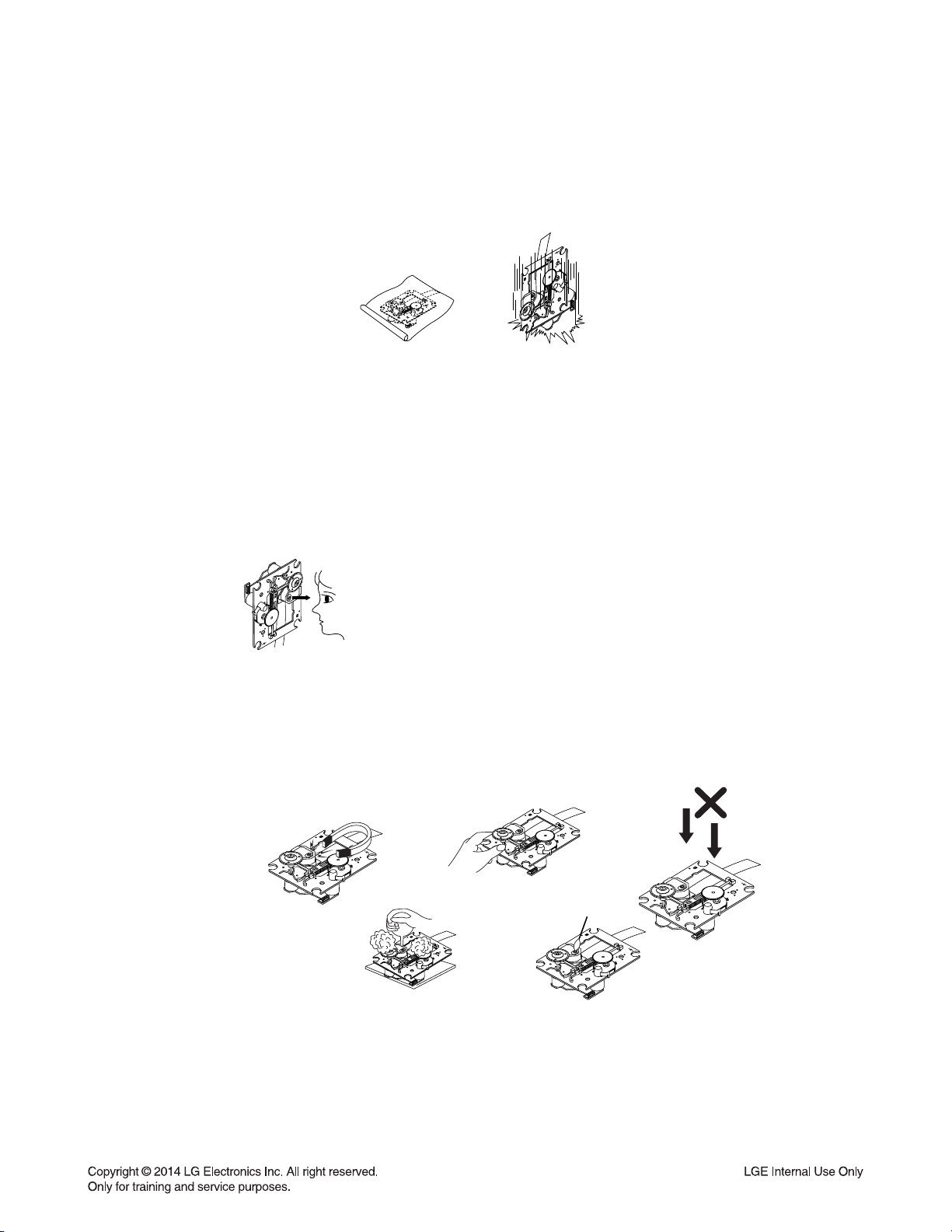
NOTES REGARDING HANDLING OF THE PICK-UP
1. Notes for transport and storage
1) The pick-up should always be left in its conductive bag until immediately prior to use.
2) The pick-up should never be subjected to external pressure or impact.
Storage in conductive bag
Drop impact
2. Repair notes
1) The pick-up incorporates a strong magnet, and so should never be brought close to magnetic materials.
2) The pick-up should always be handled correctly and carefully, taking care to avoid external pressure and
impact. If it is subjected to strong pressure or impact, the result may be an operational malfunction and/or
damage to the printed-circuit board.
3) Each and every pick-up is already individually adjusted to a high degree of precision, and for that reason
the adjustment point and installation screws should absolutely never be touched.
4) Laser beams may damage the eyes!
Absolutely never permit laser beams to enter the eyes!
Also NEVER switch ON the power to the laser output part (lens, etc.) of the pick-up if it is damaged.
NEVER look directly at the laser beam, and don’t allow
contact with fingers or other exposed skin.
5) Cleaning the lens surface
If there is dust on the lens surface, the dust should be cleaned away by using an air bush (such as used
for camera lens). The lens is held by a delicate spring. When cleaning the lens surface, therefore, a cotton
swab should be used, taking care not to distort lens.
Pressure
Magnet
How to hold the pick-up
Cotton swab
Conductive Sheet
6) Never attempt to disassemble the pick-up.
Spring has excess pressure. If the lens is extremely dirty, apply isopropyl alcohol to the cotton swab.
(Do not use any other liquid cleaners, because they will damage the lens.) Take care not to use too much
of this alcohol on the swab, and do not allow the alcohol to get inside the pick-up.
1-3
Pressure
Page 5
NOTES REGARDING COMPACT DISC PLAYER REPAIRS
1. Preparations
1) Compact disc players incorporate a great many ICs as well as the pick-up (laser diode). These components
are sensitive to, and easily affected by, static electricity. If such static electricity is high voltage, components
can be damaged, and for that reason components should be handled with care.
2) The pick-up is composed of many optical components and other high-precision components. Care must be
taken, therefore, to avoid repair or storage where the temperature or humidity is high, where strong magnetism is present, or where there is excessive dust.
2. Notes for repair
1) Before replacing a component part, first disconnect the power supply lead wire from the unit
2) All equipment, measuring instruments and tools must be grounded.
3) The workbench should be covered with a conductive sheet and grounded.
When removing the laser pick-up from its conductive bag, do not place the pick-up on the bag. (This is
because there is the possibility of damage by static electricity.)
4) To prevent AC leakage, the metal part of the soldering iron should be grounded.
5) Workers should be grounded by an armband (1 MΩ)
6) Care should be taken not to permit the laser pick-up to come in contact with clothing, in order to prevent static electricity changes in the clothing to escape from the armband.
7) The laser beam from the pick-up should NEVER be directly facing the eyes or bare skin.
Armband
Resistor
(1 MΩ)
Resistor
(1 MΩ)
Conductive
Sheet
1-4
Page 6
ESD PRECAUTIONS
Electrostatically Sensitive Devices (ESD)
Some semiconductor (solid state) devices can be damaged easily by static electricity. Such components
commonly are called Electrostatically Sensitive Devices (ESD). Examples of typical ESD devices are integrated
circuits and some field-effect transistors and semiconductor chip components. The following techniques should
be used to help reduce the incidence of component damage caused by static electricity.
1. Immediately before handling any semiconductor component or semiconductor-equipped assembly, drain off
any electrostatic charge on your body by touching a known earth ground. Alternatively, obtain and wear a
commercially available discharging wrist strap device, which should be removed for potential shock reasons
prior to applying power to the unit under test.
2. After removing an electrical assembly equipped with ESD devices, place the assembly on a conductive surface
such as aluminum foil, to prevent electrostatic charge buildup or exposure of the assembly.
3. Use only a grounded-tip soldering iron to solder or unsolder ESD devices.
4. Use only an anti-static solder removal device. Some solder removal devices not classified as "anti-static" can
generate electrical charges sufficient to damage ESD devices.
5. Do not use freon-propelled chemicals. These can generate electrical charges sufficient to damage ESD
devices.
6. Do not remove a replacement ESD device from its protective package until immediately before you are
ready to install it. (Most replacement ESD devices are packaged with leads electrically shorted together by
conductive foam, aluminum foil or comparable conductive materials).
7. Immediately before removing the protective material from the leads of a replacement ESD device, touch the
protective material to the chassis or circuit assembly into which the device will by installed.
CAUTION : BE SURE NO POWER IS APPLIED TO THE CHASSIS OR CIRCUIT, AND OBSERVE ALL OTHER
SAFETY PRECAUTIONS.
8. Minimize bodily motions when handing unpackaged replacement ESD devices. (Otherwise harmless motion
such as the brushing together of your clothes fabric or the lifting of your foot from a carpeted floor can generate
static electricity sufficient to damage an ESD device).
CAUTION. GRAPHIC SYMBOLS
THE LIGHTNING FLASH WITH APROWHEAD SYMBOL. WITHIN AN EQUILATERAL TRIANGLE, IS
INTENDED TO ALERT THE SERVICE PERSONNEL TO THE PRESENCE OF UNINSULATED
“DANGEROUS VOLTAGE” THAT MAY BE OF SUFFICIENT MAGNITUDE TO CONSTITUTE A RISK OF
ELECTRIC SHOCK.
THE EXCLAMATION POINT WITHIN AN EQUILATERAL TRIANGLE IS INTENDED TO ALERT THE
SERVICE PERSONNEL TO THE PRESENCE OF IMPORTANT SAFETY INFORMATION IN SERVICE
LITERATURE.
1-5
Page 7

HIDDEN KEY MODE
Push both Front key and RCU key to activate it for 5 seconds.
1. Disc Lock On/Off (CD Function Only Active)
Front Key : STOP
RCU Key : STOP
2. Check Version and Option code
Front Key : STOP
RCU Key : PLAY/PAUSE
You can change [Audio MCU Version <-> CD Controller Version <-> EEPROM Option] by SKIP+/-.
3. Clear EEPROM
Front Key : STOP
RCU Key : SKIP-
4. Edit EEPROM
Front Key : STOP
RCU Key : SKIP+
You can change the digit of option by SKIP+/-.
You can edit 0~f by REPEAT or PLAY/PAUSE key.
5. Bluetooth DUT
Front Key : STOP
RCU Key : PROGRAM
Bluetooth model only
6. Power Disc Lock On/Off (CD Function Only Active)
Front Key : STOP
RCU Key : EQ
7. Amp Clip On/Off
Front Key : STOP
RCU Key : Mute
Amp Clip Mode Change (Amp Clip On --> Amp Clip Off --> Level Down display)
1-6
Page 8
SERVICE INFORMATION FOR EEPROM
POWER ON
FLD “NO DISC” status
It is possible at any function.
(ex. It is possible at FLD “NO USB” status, too.)
This is an example.
Remote control ‘ ’ + Front ‘STOP’
push same timing during 5 seconds.
FLD “op0-…..”
Move to appropriate position and
make changes with remote control.
( , , /■ , REPEAT )
Press STOP key
FLD “WRITE OK”
DETECT NEW EEPROM
(OPTION EDIT SCREEN)
NAME
OP0
OP1
OP2
OP3
OP4
OP5
OP6
OP7
OP8
OP9
HEX
05
00
00
00
00
01
81
46
00
01
Remote control ‘ ’ +
Front ‘STOP’ push same timing.
FLD “e2p clr”
Completed
1-7
Page 9
PROGRAM DOWNLOAD & UPDATE GUIDE
1. AUDIO PROGRAM
Download program file name must be MICOM_CM9540_YYMMDDX.HEX
If security program (Water Wall) is activated on your PC, you must save the file to the USB storage device and
disable the security software, then download the file to your set. Downloading file proceeds in the same way at
USB1 function and USB2 function.
Caution: When downloading the file, you should neither unplug the USB device, change to the other function,
nor power off the device. USB device must be unplugged when the downloading process is completed.
ON VFD DISPLAY SCREEN
NO USB
↓← Insert USB device at USB function.
SEARCH
↓
MICOM UP
↓
FINISH
↓
Auto POWER OFF
1-8
Page 10
2. CD PROGRAM
Download program file name must be HG480_CM9540_YYMMDDX.bin
If security program (Water Wall) is activated on your PC, you must save the file to the USB storage device and
disable the security software, then download the file to your set. Downloading file proceeds in the same way at
USB1 function and USB2 function.
Caution: When downloading the file, you should neither unplug the USB device, change to the other function,
nor power off the device. USB device must be unplugged when the downloading process is completed.
ON VFD DISPLAY SCREEN
NO USB
↓← Insert USB device at USB function.
SEARCH
↓
MCS UP
↓
SMJ UP
↓
FINISH
↓
Auto POWER OFF
1-9
Page 11

3. DEMO PROGRAM
Download program file name must be DEMO_DAT.bin
If security program (Water Wall) is activated on your PC, you must save the file to the USB storage device and
disable the security software, then download the file to your set. Downloading file proceeds in the same way at
USB1 function and USB2 function.
Caution: When downloading the file, you should neither unplug the USB device, change to the other function,
nor power off the device. USB device must be unplugged when the downloading process is completed.
ON VFD DISPLAY SCREEN
NO USB
↓← Insert USB device at USB function.
SEARCH
↓
DEMO UP
↓
FINISH
↓
Auto POWER OFF
1-10
Page 12
4. EQ PROGRAM
Download program file name must be EQ_PRG.BIN
If security program (Water Wall) is activated on your PC, you must save the file to the USB storage device and
disable the security software, then download the file to your set. Downloading file proceeds in the same way at
USB1 function and USB2 function.
Caution: When downloading the file, you should neither unplug the USB device, change to the other function,
nor power off the device. USB device must be unplugged when the downloading process is completed.
ON VFD DISPLAY SCREEN
NO USB
↓← Insert USB device at USB function.
SEARCH
↓
EQ UP
↓
FINISH
↓
Auto POWER OFF
1-11
Page 13

SPECIFICATIONS
• GENERAL
Power requirements Refer to the main label.
Power consumption Refer to the main label.
Dimensions (W x H x D) (290 x 349 x 370) mm
Net Weight (Approx.) 5.9 kg
Operating temperature 5 °C to 35 °C (41 °F to 95 °F)
Operating humidity 60 %
Bus Power Supply 5 V 500 mA
• INPUTS
AUX IN 2.0 Vrms (1 kHz, 0 dB), 600 Ω, RCA jack (L, R)
PORT. IN 1.2 Vrms (3.5 mm stereo jack)
MIC 20 mV
• TUNER
FM Tuning Range 87.5 to 108.0 MHz or 87.50 to 108.00 MHz
AM Tuning Range 522 to 1 620 kHz, 520 to 1 710 kHz or 522 to 1 710 kHz
• CD
Frequency Response 40 to 20 000 Hz
Signal-to-noise ratio 75 dB
Dynamic range 80 dB
• AMPLIFIER
Stereo mode 385 W x 2 (THD 20 %)
Surround mode
Front 385 W x 2 (THD 20 %)
Surround 385 W x 2 (THD 20 %)
Subwoofer 385 W x 2 (THD 20 %)
• FRONT SPEAKER
Type 2 Way 2 Speaker
Impedance 6 Ω
Rated Input Power 385 W
Max. Input power 770 W
• SURROUND SPEAKER
Type 1 Way 1 speaker
Impedance 6 Ω
Rated Input Power 385 W
Max. Input power 770 W
Net Dimensions (W x H x D) (425 x 505 x 351) mm
Net Weight 13.2 kg
• SUBWOOFER
Type 1 Way 1 speaker
Impedance 6 Ω
Rated Input Power 385 W
Max. Input power 770 W
Net Dimensions (W x H x D) (425 x 505 x 354) mm
Net Weight 12.7 kg
• Design and specifications are subject to change without notice.
1-12
Page 14

SECTION 2
CABINET & MAIN CHASSIS
CONTENTS
EXPLODED VIEWS ..................................................................................................................................... 2-3
1. CABINET AND MAIN FRAME SECTION (CM9540) ................................................................................ 2-3
2. MECHANISM DECK SECTION (DP17TM2) ............................................................................................ 2-5
3. PACKING ACCESSORY SECTION ......................................................................................................... 2-7
4. SPEAKER SECTION ................................................................................................................................ 2-8
2-1
Page 15

MEMO
2-2
Page 16
EXPLODED VIEWS
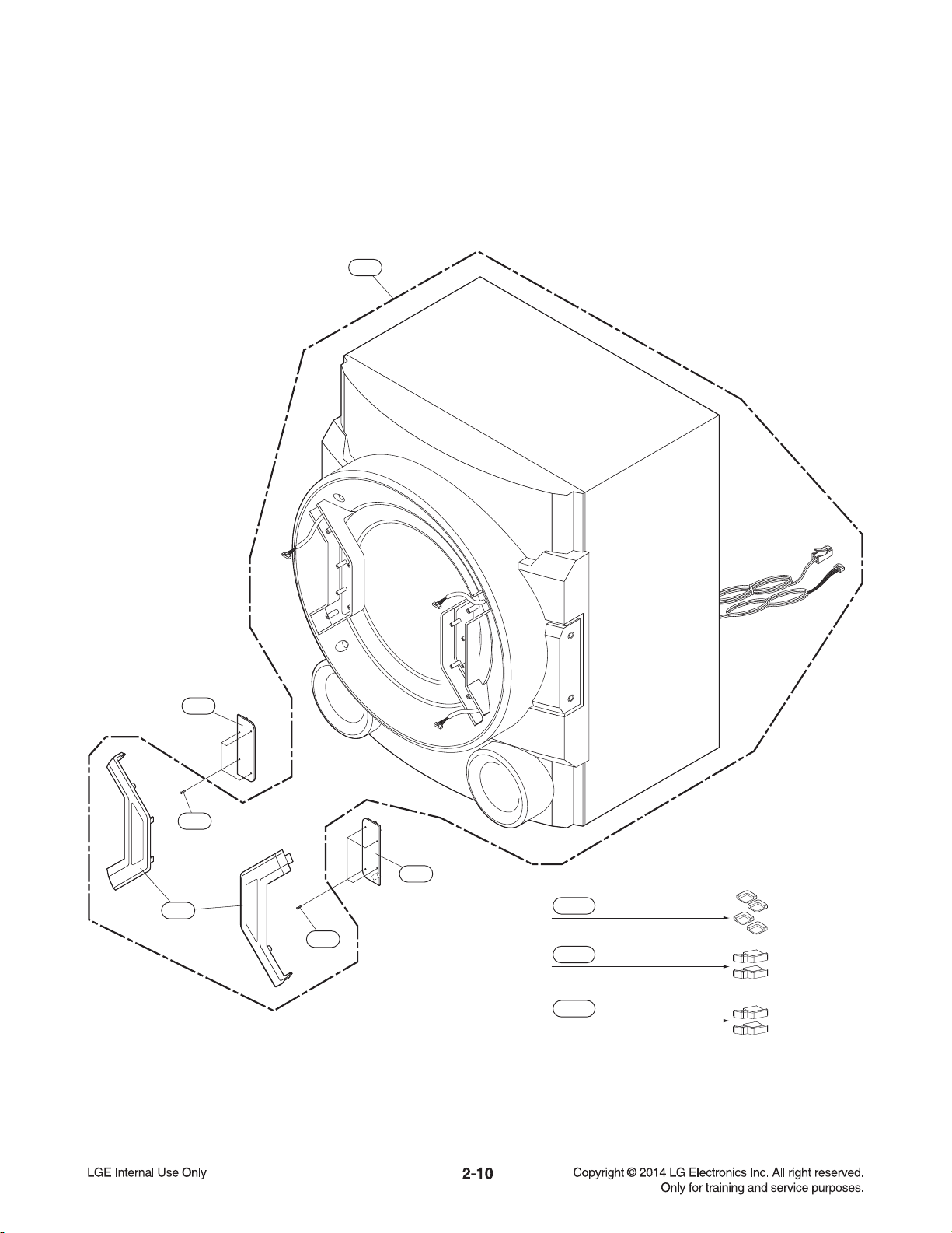
1. CABINET AND MAIN FRAME SECTION (CM9540)
M
B
A
H
G
D
E
F
MAIN
A
E
D
B
L
SMPS
M
266
A46
267
443
443
252
251
252
253
A42
A47
443
443
443
268
270
269
272
271
443
443
443
443
443
F
B/T
A52
CABLE4
A44
259
K
MIC & PTB
443
CABLE3
G
H
I
J
443
443
CABLE1
FRONT
CABLE2
I
J
K
291
NFC Tag
NOTES) THE EXCLAMATION POINT WITHIN AN
EQUILATERAL TRIANGLE IS INTENDED
TO ALERT THE SERVICE PERSONNEL
TO THE PRESENCE OF IMPORTANT
SAFETY INFORMATION IN SERVICE
LITERATURE.
A43
A56
L
300
Page 17
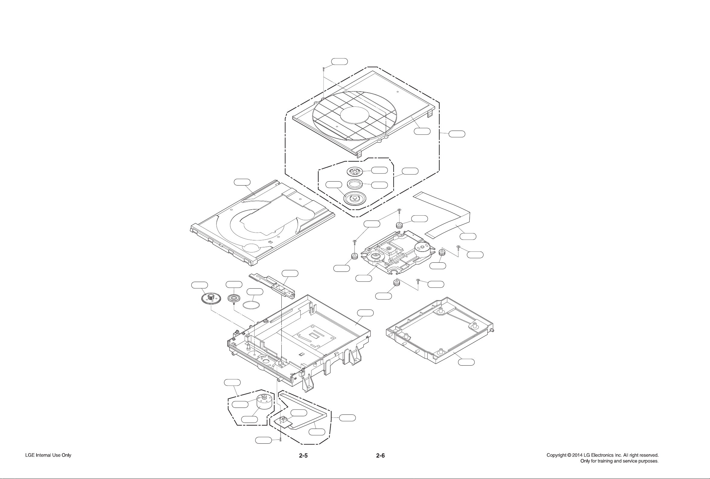
2. MECHANISM DECK SECTION (DP17TM2)
1026
1439
A001
1002
1005
1001
1049
1437
1437
1024
1024
1030
1024
1043
1045
A005
A006
1016
1013
1015
1020
1024
1003
1439
1018
1019
1011
1012
1437
1004
Page 18
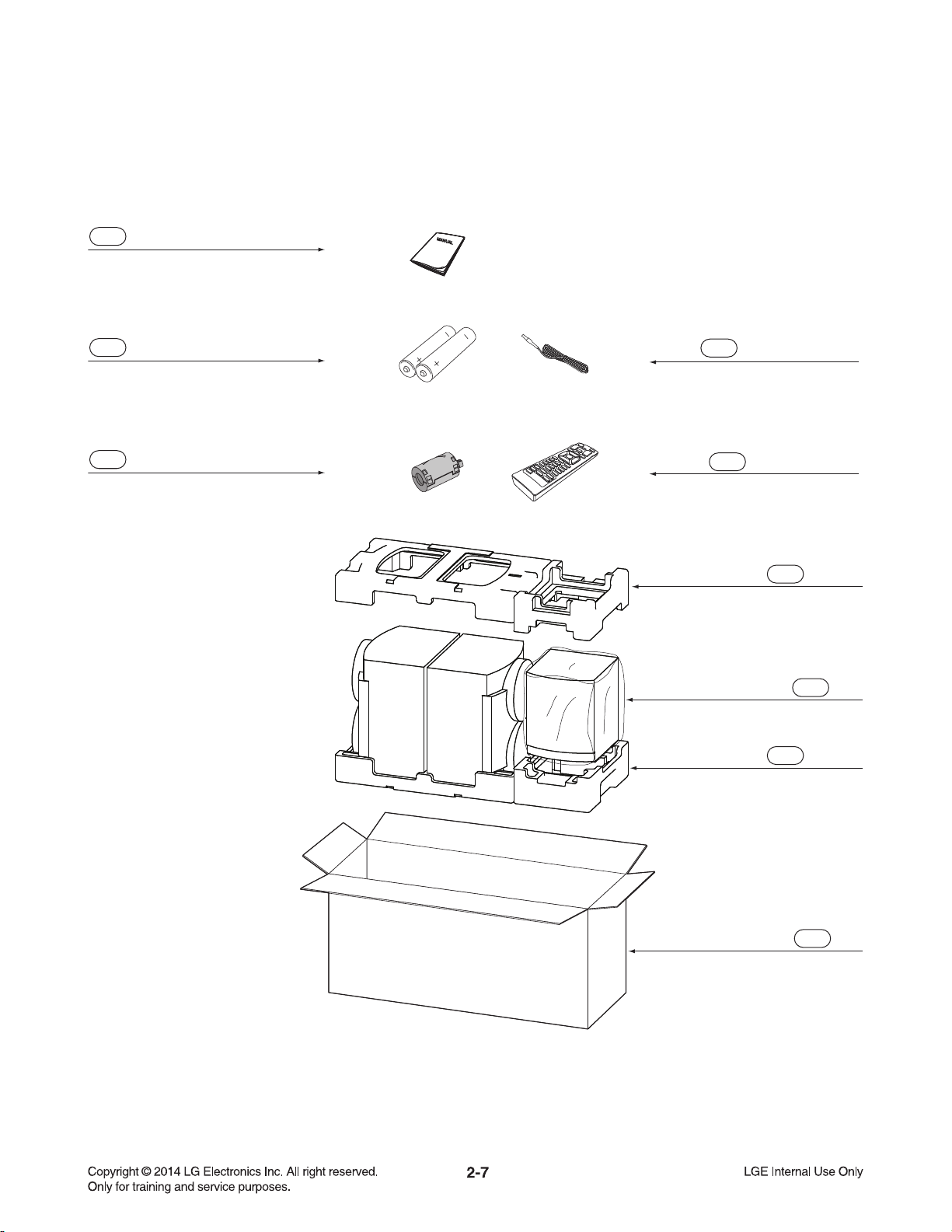
3. PACKING ACCESSORY SECTION
801 Owner’s Manual
808 Battery
826 Filter, Ferrite Core
825 FM Wire Antenna
900 Remote Control
803 Packing
804 Bag
803 Packing
802 Box
Page 19
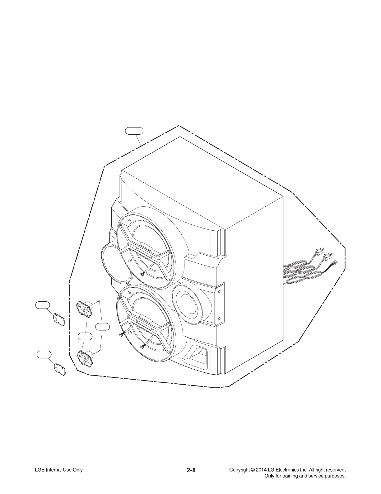
4. SPEAKER SECTION
4-1. FRONT SPEAKER (CMS9540F)
• LEFT SPEAKER
A60L
A61
A62
LED
SUB
LED
MAIN
652
651
Page 20
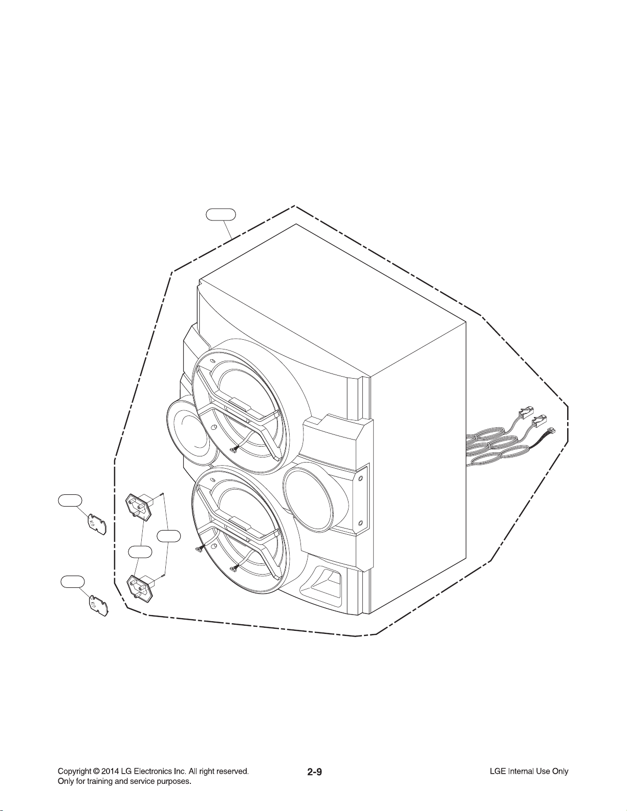
FRONT SPEAKER (CMS9540F)
• RIGHT SPEAKER
A60R
A61
A62
LED
SUB
LED
MAIN
652
651
Page 21
4-2. SUBWOOFER SPEAKER (CMS9540W)
A90
951
A91
952
LED
SUB
LED
MAIN
A92
836A Rubber Foot (Rear)
952
836L Rubber Foot (Left)
836R Rubber Foot (Right)
Page 22

SECTION 3
ELECTRICAL
CONTENTS
ONE POINT REPAIR GUIDE ............................................................................................................................ 3-2
1. NO POWER ............................................................................................................................................ 3-2
2. NO BOOTING WHEN POWER ON THE SET ....................................................................................... 3-4
3. VFD IS NOT DISPLAYED WHEN POWER ON THE SET ..................................................................... 3-5
4. NO BOOTING IN CD/USB FUNCTION .................................................................................................. 3-6
5. NO OPERATION OF MD (DRIVING THE SERVO MOTORS) ............................................................ 3-11
6. NO SOUND .......................................................................................................................................... 3-16
7. AUDIO OUTPUT IS SMALL OR NO AUDIO OUTPUT ........................................................................ 3-22
8. NO POWER ON (STANDBY LED IS BLINKING) ................................................................................ 3-23
9. SPEAKER NO AUDIO .......................................................................................................................... 3-24
ELECTRICAL TROUBLESHOOTING GUIDE ................................................................................................ 3-25
1. POWER SUPPLY ON SMPS BOARD ................................................................................................. 3-25
2. SYSTEM PART .................................................................................................................................... 3-29
3. NO AUDIO PART ................................................................................................................................. 3-30
4. NO LIGHTING (WOOFER SPEAKER) ................................................................................................. 3-35
WAVEFORMS OF MAJOR CHECK POINT ................................................................................................... 3-36
WIRING DIAGRAM ......................................................................................................................................... 3-41
BLOCK DIAGRAMS ........................................................................................................................................ 3-43
1. SMPS BLOCK DIAGRAM..................................................................................................................... 3-43
2. MAIN SYSTEM BLOCK DIAGRAM ...................................................................................................... 3-45
3. MAIN POWER BLOCK DIAGRAM ....................................................................................................... 3-47
CIRCUIT DIAGRAMS ...................................................................................................................................... 3-49
1. SMPS - POWER #1 CIRCUIT DIAGRAM ............................................................................................ 3-49
2. SMPS - POWER #2 CIRCUIT DIAGRAM ............................................................................................ 3-51
3. MAIN - CD DSP CIRCUIT DIAGRAM .................................................................................................. 3-53
4. MAIN - RF / SERVO CIRCUIT DIAGRAM ........................................................................................... 3-55
5. MAIN - ADC / PWM CIRCUIT DIAGRAM ............................................................................................ 3-57
6. MAIN - AMP CIRCUIT DIAGRAM ........................................................................................................ 3-59
7. FRONT VOLUME CIRCUIT DIAGRAM ................................................................................................ 3-61
8. MIC & PORTABLE CIRCUIT DIAGRAM .............................................................................................. 3-63
9. FRONT SPEAKER MAIN CIRCUIT DIAGRAM .................................................................................... 3-65
10. FRONT SPEAKER SUB CIRCUIT DIAGRAM ..................................................................................... 3-67
11. WOOFER SPEAKER MAIN CIRCUIT DIAGRAM ................................................................................ 3-69
12. WOOFER SPEAKER SUB CIRCUIT DIAGRAM .................................................................................. 3-71
CIRCUIT VOLTAGE CHART .......................................................................................................................... 3-73
1. CONNECTORS .................................................................................................................................... 3-73
2. CAPACITORS....................................................................................................................................... 3-74
PRINTED CIRCUIT BOARD DIAGRAMS ....................................................................................................... 3-75
1. SMPS P.C.BOARD ............................................................................................................................... 3-75
2. MAIN P.C.BOARD ................................................................................................................................ 3-79
3. FRONT VOLUME P.C.BOARD ............................................................................................................ 3-83
4. MIC & PORTABLE P.C.BOARD ........................................................................................................... 3-85
5. FRONT SPEAKER MAIN P.C.BOARD ................................................................................................ 3-85
6. FRONT SPEAKER SUB P.C.BOARD .................................................................................................. 3-85
7. WOOFER SPEAKER MAIN P.C.BOARD ............................................................................................. 3-87
8. WOOFER SPEAKER SUB P.C.BOARD .............................................................................................. 3-87
3-1
Page 23
ONE POINT REPAIR GUIDE
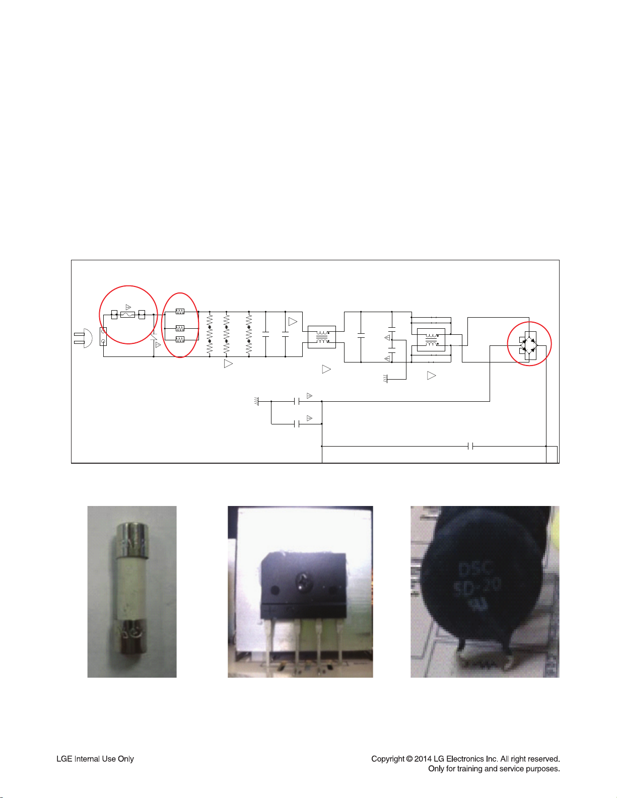
1. NO POWER
If the unit doesn’t work by no power problem, repair the set according to the following
guide.
1-1. FUSE / BRIDGE DIODE / THERMISTOR
1-1-1. Solution
Please check and replace F901, BD901, TH900, TH901 on SMPS board.
1-1-2. How to troubleshoot (Countermeasure)
1) Check if the fuse F901 is open or short-circuit.
2) Check if the bridge diode BD901 is short-circuit by over current with a digital multi meter.
3) Check if the NTC thermistor TH900, TH901 is normal or open.
PN901
FH901
12
GP390-02P-TS
T12AH/250V
(12A 250V)
F901
12
TH900
FH902
FNR-14K681T
TH901
VR900
TH902
READY
R-PART:EBG61545701
5ohm
5ohm
1M
1M
1M
R904
!
R905
R906
1M
TP13 TP14
1M
1M
GND
R901
0.22uF/275V
CM903
R902
R903
0.33uF/275V
1000pF/250VAC
R9E1
1M
TP15
R9E2
1M
TP20TP12
TP16
R9E3
1M
1-1-3. Service hint (Any picture / Remark)
!
CM901
2
8
9FL
m
R:EAE62524901
1000pF/250VAC
C903
C909
0
H
2
!
0.33uF/275V
R:EAE62524901
CM902
470pF/250VAC
C901
C902
NC
GND
J901
1
J902
1
J903
1
J904
1
2
LF901
!
2
2
2
6
C90
1uF
/550V
600V/10A
4
1
2
3
4
@Opti
2
BD901
D10XB60
1
25x15
HS906
3
< F901 >
If F901 is not short-circuit,
replace it with a same
specifi cations one.
< BD901 >
If BD901 is short-circuit,
replace it with a new one.
3-2
< TH900, TH901 >
If TH900, TH901 is open,
replace it with a new one.
Page 24
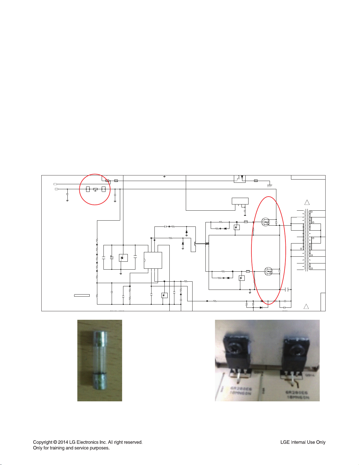
ONE POINT REPAIR GUIDE
3
R980
25deg >330ohm
NO POWER
If the unit doesn’t work by no ±PVDD problem, repair the set according to the following
guide.
1-2. NO AMP POWER
1-2-1. Solution
Please check and replace F911, Q905, Q906 on SMPS board.
1-2-2. How to troubleshoot (Countermeasure)
1) Check if the fuse F901 is open or short-circuit.
2) Check the Drain-Source or Drain-Gate, Gate-Source Resistance of Q905, Q906 with a digital multi-meter.
If it is short condition, it’s destroyed. Replace it with a new one.
(Please replace 2 FET at the same time although several FET is OK)
1-2-3. Service hint (Any picture / Remark)
PFC_TH
PFC_OUT
380V
C979
P.GND
102PF
22k VINS :285V
24k VINS :260V
FH912
12
F911
6.3A/250V
TP62
TP63
TP64
TP65
R9A6
R945
R944
R9A3
R942
R941
70deg->2.2kohm
12
MARK:G2
12
FH911
1M
1M
1M
1M
1M
1%
24K
TH912
BG
PFC_PTC_SMD
F
C932
C960 1u
C943
R951:24K=> 65KHZ
R951:20K=> 70KHZ
TH914
C978
P.GND
READY
22nF
102PF
ZD904
P.GND
C977
BZX84-C16
TP39
R927
12
10nF
R951
12
ON/OFF:11.3~12.7V
Ivcc:5.8mA
10nF
C933
IC902
2.7K
12K
TP42
TP43
6LG7HG8
VCC
ICE1HS01G-1
VCSL:0.8V
VCSH:1.63V
1
2
CS
FMIN
100nF
C942
3FB4
5
VINS
GND
Vab:5V
Vth:1.25V
ZD915
P.GND
C935
470nF
TP41
TP48
/50V
NC
R993
3.3
R992
3.3
P.GND
FBH:4.5V OVERLOAD
Fixed Blanking Time:20ms
10K
R950
TP38
10nF
C940
BZX84-C10
22nF
C939
R949
P.GND
D934
22
D935
SMFB14
SMFB14
HS905 H/S
HS904
50X15
2
3
2
4
C972
READY
P.GND
BC911
UBW2012-121F
READY
TH913
0
1G
10K
R990
GND
2D
READY
C992
3S
Q905
IPA60R190E6
!
T903
20
19
2
18
3
17
4
16
5
15
6
14
7
13
8
PC90
3
1
R986
TP46
100
R988
TP60
D932
ZD912
4.7
SMFB14
T902
CM9720 PULSE
7
10
W1
W3
W2
1
56
4
12
1G
Q906
10K
IPA60R190E6
D922
1SS355
75
D921
2D
3S
R9A7
150
1W
READY
C993
C934
0.039uF
1250V
C938
68PF
1KV/125C
C982
R9B7
100
D926
R9B8
TP61
4.7
SMFB14
R9B4
TP32
0OHM
BC915
TP47
UBW2012-121F
ZD917
READY
R9B9
P.GND
R9A8
R9C4
12
12
27T/8T:2T
230uH:65uH
!
11
< F911 >
If F911 is not short-circuit,
replace it with a same specifi cations one.
< Q905, Q906 >
If Q905, Q906 is short-circuit,
replace it with a new one.
3-3
Page 25
ONE POINT REPAIR GUIDE
2. NO BOOTING WHEN POWER ON THE SET
The set doesn’t work when press the power button on the front board or the remote
control.
2-1. MICOM (IC501)
2-1-1. Solution
Please check and replace IC501 on MAIN board.
2-1-2. How to troubleshoot (Countermeasure)
1) Check the 5.6 VA (CN106) and DVCC 3.3 V(IC505) in standby mode.
If there is no 5.6 VA, check the SMPS and if doesn’t appear 3.3 V, check IC505.
2) Check 5.6 VA, +12 V, FL+, FL-, an +39 V when power on the set.
-
If the set doesn’t work regardless of what the KEY2 changes high to low while pressing the power button.
X500 and X501 work normally but, if you can not power on the set, replace the IC501 with a new one on
the main board.
2-1-3. Service hint (Any picture / Remark)
\WX
rlX
O X]P
OZYU^]_ro¡P
< MAIN board top view >
\WW
OY[to¡P
w~yj{ys
Oy\m^P
3-4
Page 26
ONE POINT REPAIR GUIDE
3. VFD IS NOT DISPLAYED WHEN POWER ON THE SET
When power on the set, any icons or characters on VFD are not displayed.
3-1. VFD (DIG300)
3-1-1. Solution
Please check and replace DIG300 on FRONT board.
3-1-2. How to troubleshoot (Countermeasure)
1) Check if 39V, FL+ and FL-are output from SMPS to VFD via the main board.
2) Check if the IC101 outputs VFD_RST, VFD_CLK, VFD_STB, and VFD_STB to the front board.
3) Check if the VFD grid current amplifier circuit (Q301, Q303) on the front board.
Check the drive signal to the transistor’s base.
If the control signals from VFD (DGND_2, VH, VDD) isn’t output, replace VFD with a new one.
If the transistor doesn’t work, replace it.
3-1-3. Service hint (Any picture / Remark)
kpnZWXG} mk
{w ZWYSG
{w ZWZSG
{wZW[
xZWX xZW[xZWZ
yZY^O{w ZW[P
xZWXGl
j G G SG G GGG
GU
GGGG U
G
ZW} T
< MAIN board top view >
3-5
Page 27

ONE POINT REPAIR GUIDE
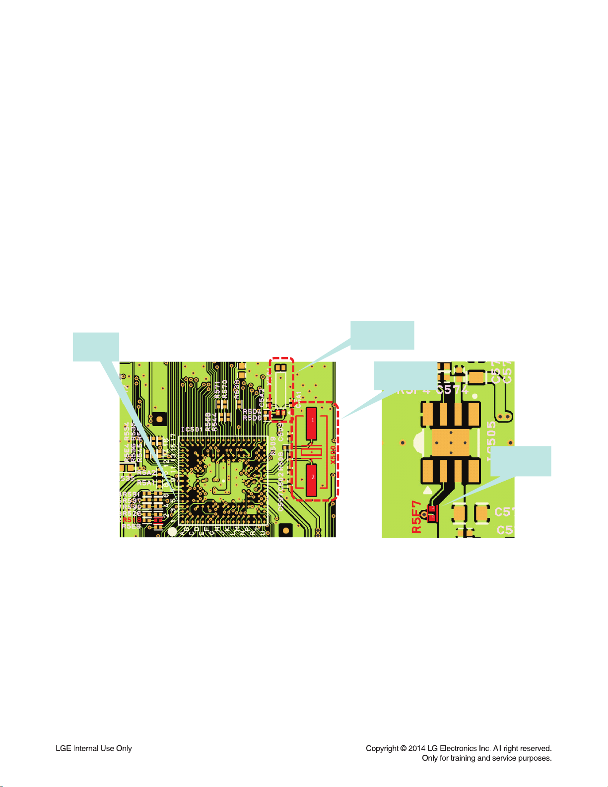
4. NO BOOTING IN CD/USB FUNCTION
After you turn on power key and displayed message in the following order
(HELLO --> VOL XX --> CD or USB) on VFD,
it will not display other message on VFD, and it will not boot-up normally.
4-1. NO VCC33, VCC12
4-1-1. Solution
Please check and replace IC505, IC509 on MAIN board.
4-1-2. How to troubleshoot (Countermeasure)
1) Check voltage of IC505 pin3 on MAIN board.
If IC505 pin3 (about 4.9 V) & D500 Input 5.6 VA doesn’t come out, check 5.6 VA from SMPS board.
2) If IC505 pin3 (about 4.9 V) is normal, check the PWR_CTRL (IC505 pin2) is high (about 3.3 V).
If PWR_CTRL isn’t high, check pinB2 of IC501 & R524, R5F7.
3)
If PWR_CTRL is high, check R5F6, R5F4, R5F5 and if there’s no defective component then replace IC505.
4) If 3.3 V (VCC33) is normal, check 1.2 V output (pin2, 4) voltage of IC509.
If 1.2 V of IC509 pin2, 4 doesn’t come out, then replace IC509.
4-1-3. Service hint (Any picture / Remark)
IC505
D501
IC509
< MAIN board top view >
3-6
Page 28

ONE POINT REPAIR GUIDE
NO BOOTING IN CD/USB FUNCTION
After you turn on power key and displayed message in the following order
(HELLO --> VOL XX --> CD or USB) on VFD,
it will not display other message on VFD, and it will not boot-up normally.
4-2. CRYSTAL (X500)
4-2-1. Solution
Please check and replace X500 on MAIN board.
4-2-2. How to troubleshoot (Countermeasure)
1) If 3.3 V & 1.2 V is normal, check Reset ‘High’ of IC501 pinT12 on MAIN board.
If MAIN_RESET isn’t high, check MICOM (IC101) pin40.
2) If MAIN_RESET is high, check the soldering status of 24 MHz crystal (X500).
3) If the crystal (X500) doesn’t oscillate, check R508, R509, C502, C503 around crystal (X500).
If there’s no defective component, then replace X500.
4-2-3. Service hint (Any picture / Remark)
X500
< Signal check point >
p
v
IC500
< Signal waveform >
3-7
Page 29

ONE POINT REPAIR GUIDE
NO BOOTING IN CD/USB FUNCTION
After you turn on power key and displayed message in the following order
(HELLO --> VOL XX --> CD or USB) on VFD,
it will not display other message on VFD, and it will not boot-up normally.
4-3. SERIAL FLASH (IC503)
4-3-1. Solution
Please check and replace IC503 on MAIN board.
4-3-2. How to troubleshoot (Countermeasure)
1) If the crystal (X500) does oscillate, check serial flash (IC503) on MAIN board.
Check pin8(VCC), pin6(CLK), pin1(CS), pin2(DO), pin5(DI) of below waveform.
2) If pin1, 2, 5, 6, 8 doesn’t come out, check damping resistor (R564, R563, R535, R536, R534) of IC503.
If damping resistor of IC503 is OK, then replace IC503. (it need to download program)
3) After change IC503, if it is still not below waveform, check IC501(DSP IC).
4-3-3. Service hint (Any picture / Remark)
VCC
IC503
CS#
CLK
DO
< Signal check point > < Signal waveform >
3-8
Page 30

ONE POINT REPAIR GUIDE
NO BOOTING IN CD/USB FUNCTION
After you turn on power key and displayed message in the following order
(HELLO --> VOL XX --> CD or USB) on VFD,
it will not display other message on VFD, and it will not boot-up normally.
4-4. SDRAM (IC502)
4-4-1. Solution
Please check and replace IC502 on MAIN board.
4-4-2. How to troubleshoot (Countermeasure)
1) Check below waveform & soldering status of SDRAM (IC502) on MAIN board.
If pin17(#CAS), pin18(#RAS), pin19(#CS), pin38(CLK), pin29(address), pin2(DQ) doesn’t come out,
check damping resistor (R568, R506, R570, R544, R547).
2) If resistor is OK, then replace IC502 (SDRAM).
3) After change IC502, if it is still not below waveform, check IC501 (DSP IC).
4-4-3. Service hint (Any picture / Remark)
IC502
< Signal check point >
}jj
y
Vjz
yhz
V~l
jhz
< Signal waveform >
3-9
Page 31

ONE POINT REPAIR GUIDE
NO BOOTING IN CD/USB FUNCTION
After you turn on power key and displayed message in the following order
(HELLO --> VOL XX --> CD or USB) on VFD,
it will not display other message on VFD, and it will not boot-up normally.
4-5. DSP IC (IC501)
4-5-1. Solution
Please check and replace IC501(MLC3730) on MAIN board.
4-5-2. How to troubleshoot (Countermeasure)
1) After check them by previous pages about no booting, if the set is still no booting,
Check soldering status of IC501.
2) If below bootstrap waveform doesn’t come out, then replace IC501(DSP IC).
4-5-3. Service hint (Any picture / Remark)
R546
R594
PGPB12
(Yellow)
IC501
y\`[
y\`_
y\`^GOiP
< Signal check point >
R598
PAD19
(Green)
R597
PAD20
(Pink)
< Signal waveform >
3-10
Page 32

ONE POINT REPAIR GUIDE
5. NO OPERATION OF MD (DRIVING THE SERVO MOTORS)
When no sound output in the CD function, you can not listen to music reading data
from a CD disc if the servo motors in MD don’t work. This step is for checking the
SPINDLE MOTOR among them.
5-1. SPINDLE MOTOR
5-1-1. Solution
Please check and replace IC407, IC408 on MAIN board.
5-1-2. How to troubleshoot (Countermeasure)
1) Check the SPDO signal from Pin16 of IC407.
If no signal, check 3.3 V(RF) and X400.
2) Check the SP- & SP+ from IC408 to CN405 for driving SPINDLE motor. It is about 3.6 Vp-p.
If no signal, check +1.8 V and +5 V for IC408.
3) Check if the FFC cable is solidly connected between CN405 and MD.
4) Check the MD.
If the spindle motor is sort-circuit or has any trouble, it can not rotate CD discs.
Please check the function after changing another MD.
5-1-3. Service hint (Any picture / Remark)
zwR
zwT
< Waveform of SP- & SP+
for driving SPINDLE motor >
zwT
_GGju[W\
zwR
w]GGju[W\
pj[W_
< Signal check point >
3-11
Page 33

ONE POINT REPAIR GUIDE
NO OPERATION OF MD (DRIVING THE SERVO MOTORS)
When no sound output in the CD function, you can not listen to music reading data
from a CD disc if the servo motors in MD don’t work. This step is for checking the
SLED MOTOR among them.
5-2. SLED MOTOR
5-2-1. Solution
Please check and replace IC407, IC408 on MAIN board.
5-2-2. How to troubleshoot (Countermeasure)
1) Check the SLDO signal from Pin23 of IC407.
If no signal, check 3.3 V(RF) and X400.
2) Check the SLED+ & SLED- from IC408 to CN405 for driving SPINDLE motor. It is about 2.9 Vp-p.
If no signal, check +1.8 V and +5 V for IC408.
3) Check if the FFC cable is solidly connected between CN405 and MD.
4) Check the MD.
If the sled motor is sort-circuit or has any trouble, it can not move the pick-up module.
Please check the function after changing another MD.
5-2-3. Service hint (Any picture / Remark)
zsR
zsT
< Waveform of SLED- & SLED+
for driving SLED motor >
zsT
`GGju[W\
zsR
^GGju[W\
pj[W_G
< Signal check point >
3-12
Page 34

ONE POINT REPAIR GUIDE
NO OPERATION OF MD (DRIVING THE SERVO MOTORS)
When no sound output in the CD function, you can not listen to music reading data
from a CD disc if the servo motors in MD don’t work. This step is for checking the
TRAY OPEN/ CLOSE MOTOR among them.
5-3. TRAY OPEN / CLOSE MOTOR
5-3-1. Solution
Please check and replace IC407, IC408 on MAIN board.
5-3-2. How to troubleshoot (Countermeasure)
1) Check MOT_OPEN & MOT_CLOSE signals from Pin K4 & L4 of IC501 to IC408.
If no signal, check +1.8 V & + 5 V to IC408.
2) Check LOAD± from IC408 to CN405 for driving the tray open / close motor. It is about 3.85 Vp-p.
If no signal, check +5 V to IC408. If it has any trouble, replace it with a new one.
3) Check if the FFC cable is solidly connected between CN405 and MD.
4) Check the MD.
If the tray motor is sort-circuit or has any trouble, it can not open or close the tray.
Please check the function after changing another MD.
5-3-3. Service hint (Any picture / Remark)
svT
svROylkP
tv{ vw lu
tv{ jsvz l
< Waveform for driving TRAY
open/close motor >
svT
wGYGGGju[W\
< Signal check point >
svR
wG[GGju[W\
tv{vwlu
^GGpj[W_
pj[W_G
tv{jsvzl
]GGpj[W_
3-13
Page 35

ONE POINT REPAIR GUIDE
NO OPERATION OF MD (DRIVING THE SERVO MOTORS)
When no sound output in the CD function, you can not listen to music reading data
from a CD disc if the pickup module in MD doesn’t work. This step is for checking the
LASER TRACKING ACTUATOR.
5-4. LASER TRACKING ACTUATOR
5-5-1. Solution
Please check and replace IC407, IC408 on MAIN board.
5-4-2. How to troubleshoot (Countermeasure)
The tracking actuator makes the laser beam be positioned in the center of a track on CD disc.
1) Check the TRD signal from Pin22 of IC407.
If no signal, check 3.3 V(RF) and X400.
2) Check TR- & TR+ from IC408 to CN404 for driving the tracking actuator.
If no signal, check +1.8 V and +5 V for IC408.
3) Check if the FFC cable is solidly connected between CN404 and MD.
4) Check the MD.
If the pick-up module has any trouble, it can not move the laser beam on the left or right side.
Please check the function after changing another MD.
5-4-3. Service hint (Any picture / Remark)
{y T Gju[W[
{y RGGju[W[
< Waveform of TR±
for driving TRACKING actuator >
{yT
X^GGju[W[
< Signal check point >
{yR
X]GGju[W[
ju[W[
3-14
Page 36

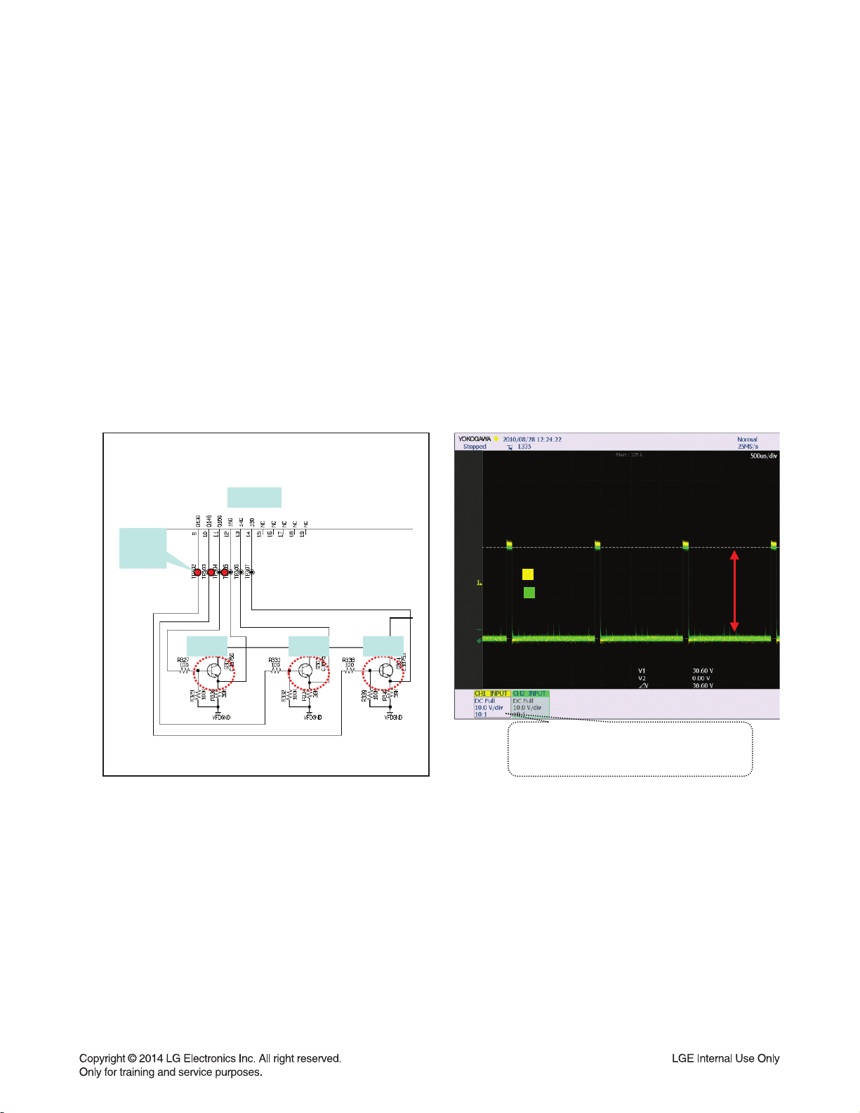
ONE POINT REPAIR GUIDE
NO OPERATION OF MD (DRIVING THE SERVO MOTORS)
When no sound output in the CD function, you can not listen to music reading data
from a CD disc if the pickup module in MD doesn’t work. This step is for checking the
LASER FOCUSING ACTUATOR.
5-5. LASER FOCUSING ACTUATOR
5-5-1. Solution
Please check and replace IC407, IC408 on MAIN board.
5-5-2. How to troubleshoot (Countermeasure)
The focusing actuator makes the laser beam keep a regular interval with the surface of a CD disc.
1) Check the FOD signal from Pin21 of IC407.
If no signal, check 3.3 V(RF) and X400.
2) Check F- & F+ from IC408 to CN404 for driving the focusing actuator.
If no signal, check +1.8 V and +5 V for IC408.
3) Check if the FFC cable is solidly connected between CN404 and MD.
4) Check the MD.
If the pick-up module has any trouble, it can not move the laser beam on the top or bottom side.
Please check the function after changing another MD.
5-5-3. Service hint (Any picture / Remark)
mRG Gju[W[
mT Gju[W[
< Waveform of F±
for driving FOCUSING actuator >
mT
X_GGju[W[
< Signal check point >
mR
X\GGju[W[
ju[W[
3-15
Page 37

ONE POINT REPAIR GUIDE
6. NO SOUND
There is no sound output in the USB FUNCTION, repair the set according to the following
guide.
6-1. IN THE USB FUNCTION
6-1-1. Solution
Please check and replace IC501 on MAIN board & IC300 on USB board.
6-1-2. How to troubleshoot (Countermeasure)
1) Check +5VU to USB board.
If +5.6 VA to pin2 of IC300(LDO) doesn’t come out, check pin4, 5 of CN304.
If +5.6 VA is normal & +5VU of IC300 pin3 doesn’t come out, then replace IC300.
2) Check if “Digital audio AMP block”.
6-1-3. Service hint (Any picture / Remark)
kR
< USB function signal fl ow >
kT
< Waveform of USB D± signal >
USB D+ / D- (CN502 Pin1, 2 & 9, 10)
3-16
Page 38

ONE POINT REPAIR GUIDE
NO SOUND
There is no sound output in the AUX FUNCTION, repair the set according to the following guide.
6-2. IN THE AUX FUNCTION
6-2-1. Solution
Please check and replace IC202 on MAIN board.
6-2-2. How to troubleshoot (Countermeasure)
1) Check AUX_L/R signals to IC202 (Pin7, 8).
2) Check if MCS_BCLK, MCS_LRCLK, & MCS_MCLK are entered from IC501 to IC202.
3) Check if ADC/MIC_DATA is entered from IC202 to IC501.
If no signal, check +5 V & +3.3 V(ADC) for IC202. If is NG, replace it a new one.
4) Check the following I2S signal flow from IC501 to IC600.
If there is any trouble, check the power for each IC. The power is normal but, if the signal waveform to
the IC is distorted or no signal, replace it with a new one.
5) Check if the digital audio AMP block is okay.
If AMP is damaged, replace it with a new one.
6-2-3. Service hint (Any picture / Remark)
CS5346
MCS_MCLK
IC501
MLC3730
{T
IC202
AUX_ L/R
ADC/MIC_ DATA
MCS_BCK
MCS_LRCK
MIX_DATA_OUT
IC600
TAS5548
PWM
< AUX function signal fl ow >
AUX
IR A MP
IRS2092+ IRF6775
tjz tjsrGGyYYX
hkjVtpjkh{hGG GyYX\tjz ijrGGyYX]
tjz syjrGGy YX`
pjYWY
< Signal check point >
w{sGGYX
w{yGGYY
3-17
Page 39

ONE POINT REPAIR GUIDE
NO SOUND
There is no sound output in the PORT. IN FUNCTION, repair the set according to the
following guide.
6-3. IN THE PORT. IN FUNCTION
6-3-1. Solution
Please check and replace IC202 on MAIN board.
6-3-2. How to troubleshoot (Countermeasure)
1) Check PT_L/R signal from JOG board to MAIN board.
2) Check if PT_LR is entered pin 4 & 5 of CN3J01 pin 4 & 5 of CN3V02 Pin21 & 20 of CN3V01.
3) Check POT_L/R signals to IC202(pin21, 22).
4) Check if ADC_BCK, ADC_LRCK, & DAC_MCLK are entered from IC501 to IC202.
5) Check if ADC_DATA is entered from IC202 to IC501.
If no signal, check +5 V & +3.3 V(ADC) for IC202. If is NG, replace it a new one.
6) Check the following I2S signal flow from IC501 to IC600.
If there is any trouble, check the power for each IC. The power is normal but ,
if the signal waveform to the IC is distorted or no signal, replace it with a new one.
7) Check if the digital audio AMP block is okay. Refer to “Digital Audio AMP” guide.
If AMP is damaged, replace it with a new one.
6-3-3. Service hint (Any picture / Remark)
IC600
PWM
POT . IN
IR A MP
IRS2092+ IRF6775
CS5346
MCS_MCLK
IC501
MLC3730
{T
IC202
POT_L/R
ADC/MIC_ DATA
MCS_LRCK
MIX_DATA_OUT
VOLUME
Board
MCS_BCK
TAS5548
< PORT. IN function signal fl ow >
tjz tjsrGGyYYX
hkjVtpjkh{hGG GyYX\tjz ijrGGyYX]
tjz syjrGGy YX`
pjYWY
< Signal check point >
w{sGGYX
w{yGGYY
3-18
Page 40

ONE POINT REPAIR GUIDE
NO SOUND
There is no sound output in the TUNER FUNCTION, repair the set according to the
following guide.
6-4. IN THE TUNER FUNCTION
6-4-1. Solution
Please check and replace IC202, TU500 on MAIN board.
6-4-2. How to troubleshoot (Countermeasure)
1) Check if TUNER_LR is entered from Pin1 & 3 of TU101 to IC202(Pin23, 24).
If no signals, Check +3.3 V for Tuner power.
Check if the Tuner control signals (CLK, DAT, CE, RST, GPO2) are entered from IC101 to TU101.
If it doesn’t work, replace TUNER with a new one.
2) Check if MCS_BCK, MCS_LRCK, & MCS_MCLK are entered from IC501 to IC202.
3) Check if ADC_DATA is entered from IC202 to IC501.
If no signal, check +5 V & +3.3 V(ADC) for IC202. If is NG, replace it a new one.
4) Check the following I2S audio signal flow from IC501 to IC600.
If there is any trouble, check the power for each IC. The power is normal but,
if the signal waveform to the IC is distorted or no signal, replace it with a new one.
5) Check if the digital audio AMP block is okay. Refer to “Digital Audio AMP” guide.
If AMP is damaged, replace it with a new one.
6-4-3. Service hint (Any picture / Remark)
TUNER
IR A MP
IRS2092+ IRF6775
CS5346
MCS_MCLK
IC501
MLC3730
{T
IC202
TUNER _L/R
ADC/MIC_ DATA
MCS_BCK
MCS_LRCK
MIX_DATA_OUT
Jack
Board
IC600
TAS5548
PWM
< TUNER function signal fl ow >
hkjVtpjkh{hGG GyYX\tjz ijrGGyYX]
tjz tjsrGGyYYX
< Signal check point >
pjYWY
tjz syjr GGy YX`
{|ulyyG
GY[
{|ulysG
GYZ
3-19
Page 41

ONE POINT REPAIR GUIDE
NO SOUND
There is no sound output in the MIC IN FUNCTION, repair the set according to the
following guide.
6-5. IN THE MIC IN FUNCTION
6-5-1. Solution
Please check and replace IC508 on Main Board or ICM101 on MIC board.
6-5-2. How to troubleshoot (Countermeasure)
1) Check MIC_SIG signal to pin6 of CN506.
If no signal, check the signal to pin6 of CN3M01 on the MIC board.
Check if the signal is entered from pin6 of CN3M01 to MAIN board.
2) Check if MIC_SIG is entered from pin6 of CN506 to pin3 to IC506 (MIC AMP).
3) Check if the amplified signal comes out from pin4 of IC506.
If no signal output, check +12 V for IC506, replace IC506 with a new one if it has a problem.
4) Check if MIC_BCK, MIC_MLCK & MIC_LRCK is entered from IC501 to IC508.
Check if MIC_DATA is entered from pin9 of IC508 to pin7 of IC600.
If no signal, check +5 V & +3.3 V for IC508. If it is abnormal, change replace it a new one.
6) Check the following I2S signal flow from IC508 to IC600.
If there is any trouble, check the power for each IC. If the signals are abnormal, replace it a new one.
7) Check if the digital audio AMP block is okay. Refer to “Digital Audio AMP” guide.
If AMP is damaged, replace it with a new one.
6-5-3. Service hint (Any picture / Remark)
MIC IN
IR A MP
IRS2092+ IRF6775
AK5358
MCS_MCLK
IC508
IC501
MLC3730
MIG_SIG
ADC/MIC_ DATA
MCS_LRCK
MIX_DATA_OUT
IC506
S4308
MCS_BCK
Board
IC600
TAS5548
PWM
MIC
tpjz pnUGGXMYG
tpjpkh{hUGwpuG`
tpjsyjrUGwpuGXW
tpjtjsrUGwpuXX tp jijrUGw puGXY
< Signal check point >< MIC IN function signal fl ow >
3-20
Page 42

ONE POINT REPAIR GUIDE
NO SOUND
There is no sound output in the BLUETOOTH FUNCTION, repair the set according to
the following guide.
6-6. IN THE BLUETOOTH FUNCTION
6-6-1. Solution
Please check and replace IC501 on MAIN board and Bluetooth module on front panel.
6-6-2. How to troubleshoot (Countermeasure)
1) Check BT_RX, BT_TX signal to Pin5, 7 of CN504.
If no signal, check the signal to Pin5, 7 and Pin1(+3.3 V) of on the Bluetooth module and cable connection state.
If there are no signal out from module, replace new module.
2) Check if BT_RX/TX is entered from Pin5, 7 of CN504 to Pin169, 170 to IC501 (DSP).
3) Check if MIC_BCK, MIC_MLCK & MIC_O_DATA is entered from IC501 to IC600.
If no signal, check VCC12(+1.2 V) for IC501. If it is abnormal, change replace it a new one.
4) Check the following I2S signal flow from IC501 to IC600.
If there is any trouble, check the power for each IC. If the signals are abnormal, replace it a new one.
5) Check if the digital audio AMP block is okay. Refer to “Digital Audio AMP” guide.
If AMP is damaged, replace it with a new one.
6-6-3. Service hint (Any picture / Remark)
B/T Module
BT_RX,
BT_TX
IC501
MLC3730
TAS5548
MCS_BCK
MCS_LRCK
MIX_DATA_OUT
IR AM P
IRS2092+ IRF6775
IC600
PWM
< BLUETOOTH function signal fl ow >
i{ { UG G^
ju\W[
i{j{ zUGGZ
i{y{zUGG[i{ y UG G\
i{j{ zUGGX^Y
i{y{zUGGX^X
i{ { UG GX^W
i{ y UG GX]`
< Signal check point >
3-21
Page 43

ONE POINT REPAIR GUIDE
7. AUDIO OUTPUT IS SMALL OR NO AUDIO OUTPUT
Audio signal output is small or not. when you power on the Middle Power Mini
System.
7-1. IC700 ~ IC705
7-1-1. Solution
Please check and replace IC700 ~ IC705 on MAIN board.
7-1-2. How to troubleshoot (Countermeasure)
1) Please check if this system is on bass blast mode.
C, RL and RR make sound only on bass blast mode.
2) Check the IC700 ~ IC705 on your eyes.
3) Check the audio signal output check (Pin13 of IC700 ~ IC705).
First, check the Audio Data input (Pin3 of IC700 ~ IC705).
4) If the audio signal output has no output, try to change IC which has no output.
5) Lastly, check Speaker Terminal (TM701, TM702).
7-1-3. Service hint (Any picture / Remark)
< MAIN board top view >
3-22
Page 44

ONE POINT REPAIR GUIDE
8. NO POWER ON (STANDBY LED IS BLINKING)
It doesn’t turn on, and blinks standby LED(Red).
8-1. AMP FETs
8-1-1. Solution
Please check and replace Q705 ~ Q708, Q711 ~ Q718 on MAIN board.
8-1-2. How to troubleshoot (Countermeasure)
1) This symptom occurs, when DC protection is detected. Main reasons are like below.
- When Some of AMP FETs dead.
8-1-3. Service hint (Any picture / Remark)
Notice for FET service
AMP FET : IRF6775
* You can see FET after removing heatsink.
* Notice for Service
Before repair Main Assy, you need to discharge SMPS.
After then, open the connector.
You should try to change both of +/- FET and Driver IC as a pair.
- In case of RF6775, Metal case, FET Drain,
has electric potential. So be careful when you
deal with it.
3-23
Page 45

ONE POINT REPAIR GUIDE
9. SPEAKER NO AUDIO
Speaker No Audio
9-1. AMP IC
9-1-1. Solution
Please check and replace IC700 ~ IC705 on MAIN board.
9-1-2. How to troubleshoot (Countermeasure)
1) Check supply voltage of AMP(CN110) & PWM signal
Normal Supply voltage and signal Check AMP IC.
Poor supply voltage Check SMPS Assy.
Poor signal Check PWM IC.
2) Check CSD of FET driver IC (IRS2092 : EAN60778301).
CSD has about 5 V on normal state.
When AMP has problem, CSD is LOW state or keep change LOW to HIGH.
9-1-3. Service hint (Any picture / Remark)
ju XXWGGwpuGXSYGaGT]]}
wpuGZS[GaGwnuk
wpuG\S ]GaGR]]}
J\GwpuGGpjGTeGjzk
3-24
Page 46

ELECTRICAL TROUBLESHOOTING GUIDE
1. POWER SUPPLY ON SMPS BOARD
No output 5.6 VA
F901 normal?
YES
BD901 normal?
YES
Is the VCC
(11 V ~ 25 V) supplied to IC901
Pin4?
YES
Power line of MAIN PCB is short.
NO
NO
NO
Replace F901 (same fuse).
Replace BD901.
D960, D961 normal?
Check or replace D960, D961.
No 12 V
Is the
VCC 13 VA supplied to IC951
Pin1?
YES
Is there
‘H’ signal at IC951
Pin4?
YES
Check and replace IC951.
Or check line of MAIN PCB is short or not.
NO
NO
Check or replace D962/ D963.
Check P_CTL from μ-com.
3-25
Page 47

ELECTRICAL TROUBLESHOOTING GUIDE
No -5 V
VCC -7 VA supplied to IC953
Is the
Pin2?
YES
Is there
‘H’ signal at Q953
Base?
YES
Check or replace Q953, Q957.
Or check line of MAIN PCB is short or not.
No output VFD
NO
NO
R965 normal?
YES
Check or replace Q951.
Check P_CTL from μ-com.
NO
Check or replace R965 / D959.
R968 normal?
YES
D957, D959 normal?
YES
ZD951, ZD952 normal?
YES
Check line of FRONT PCB is short or not.
NO
NO
NO
Replace R968.
Replace D957, D959.
Replace ZD951, ZD952.
3-26
Page 48

ELECTRICAL TROUBLESHOOTING GUIDE
No output AMP gate line
Is the VCC
13 VA supplied to IC952
Pin1 to Pin3?
Check and replace IC952.
Or check line of MAIN PCB is short or not.
NO
R952 normal?
YESYES
Check or replace D951, D952.
NO
Check or replace R952.
3-27
Page 49

ELECTRICAL TROUBLESHOOTING GUIDE
No AMP output
Is the
C904, C905 voltage
about 380 V?
YES
F911 normal?
NO
NO
YES
PFC P.CTL OK?
YES
Is the
VCC 12 V supplied to
IC904 Pin16?
YES
Check or replace
IC904, Q907 ~ Q910.
AMP P.CTL
OK?
YES
Is the
VCC 12 V supplied to
IC902 Pin8?
NO
NO
NO
NO
Check PFC P.CTL from μ-com.
Replace D908, Q955, PC903.
Check AMP P.CTL from μ-com.
Replace D908, Q956, PC902.Replace F911.
NO
Q911 ~ Q914 OK?
NO
Replace Q911 ~ Q914.
YES
Check or replace IC902
and check Q911 ~ Q914 gate(Pin2)
components (Resistors, Diodes).
3-28
Check or replace D953 ~ D956.
Check line of MAIN PCB is short or not.
Page 50

ELECTRICAL TROUBLESHOOTING GUIDE
2. SYSTEM PART
Power on.
“HELLO”
Display on FLD
OK?
YES
Volume LED
(LD3V31~LD3V40
LD3V42~LD3V49)
turn on?
NO
NO
CN301
cable connection
OK?
YES
CN301
Pin1, 3, 5
power OK?
YES
CN301
Pin9 ~ 11 data signal
OK?
YES
Q301, 303, 304
grid voltage OK?
Q301,Q303,Q304
grid voltage OK?
NO
NO
NO
NO
NO
Check 17p FFC cable.
Check SMPS board.
Check MAIN board.
Replace DIG301.
Check SMPS board.
YES
When turn the volume,
count is change?
YES
FRONT board OK.
NO
YES
CN3V01
Pin8, 9 +12 V
OK?
YES
Replace LED.
(LD3V09 ~ LD3V24)
CN3V01
pin31, 32
signal OK?
YES
Check MAIN board.
3-29
NO
NO
Check MAIN board.
Check FFC cable.
Page 51

ELECTRICAL TROUBLESHOOTING GUIDE
3. NO AUDIO PART
CD FUNCTION
Can
disc insert?
YES
Disc reading OK?
YES
NO
NO
LOAD +, - OK?
YES
Is motor impedance
about 12 Ω?
OPU driving
(Focusing & Tracking) OK?
Check OPU.
(Pick-up module)
NO
NO
NO
NO
Is motor_open/ close OK?
(IC408 Pin6, 7)
YES
Check IC501.
Check Loading motor.
Check IC408.
NO
Focusing/
Tracking/ Sled signal
OK?
YES
MON_MPD(CN404 Pin22)
about 180 mV?
Pin51, 52, 53 I2S output
IC407
signal OK?
YES
IC501
Pin N1, N2, N4 I2S input
signal OK?
YES
A
NO
NO
IC407
RF & Servo signal
OK?
YES
Check IC501.
3-30
NO
Check FFC cable
to CN404, CN405.
Page 52

ELECTRICAL TROUBLESHOOTING GUIDE
USB play
When insert USB,
IC501 PinU7,U8,A7,A8 USB_D
signal OK?
YES
A
AUX
NO
IC300
USB power +5 VU
OK?
YES
NO
Replace IC300.
Pin7, 8 AUX input signal
IC202
OK?
YES
IC202
Pin42,43,44 I2S input signal
OK?
YES
IC202 Pin41
ADC/MIC_data output signal
OK?
YES
A
NO
NO
NO
Check audio cable.
Check IC501.
Replace IC202.
3-31
Page 53

ELECTRICAL TROUBLESHOOTING GUIDE
POT. IN
Pin21,22 POT. IN input signal
IC202
OK?
YES
IC202
Pin42,43,44 I2S input signal
OK?
YES
IC202 Pin41
ADC/MIC_data output signal
OK?
YES
A
TUNER
NO
NO
NO
Check MIC board.
Check IC501.
Replace IC202.
Pin23,24 TUNER_L/R input
IC202
signal OK?
YES
IC202
Pin42,43,44 I2S input
signal OK?
YES
IC202
Pin41 ADC data output
signal OK?
YES
A
NO
NO
NO
TU500
TUNER_L/R output
signal OK?
YES
Check IC501.
Replace IC202.
3-32
NO
Check +3.3 V of TU500.
Page 54

ELECTRICAL TROUBLESHOOTING GUIDE
A
Pin D1,D2,E1 I2S clock signal
IC501
OK?
YES
IC501
Pin E2 I2S data signal
OK?
YES
IC600
PWM data output signal
OK?
YES
B
NO
NO
NO
Check IC501.
Check IC501.
Replace IC600.
3-33
Page 55

ELECTRICAL TROUBLESHOOTING GUIDE
B
Pin28,29,35,36
of IC600, FL/FR± signal
OK?
YES
IC601, 602
FL/FR audio signal
OK?
YES
Pin13 of
IC700,IC701,IC704,IC705
FL/FR audio signal
OK?
YES
IC700, IC701, IC704, IC705.
NO
Check IC600.
NO
Check IC601, IC602.
NO
Check
NO
of IC600, SWL/SWR± signal
Check IC600.
NO
SWL/SWR audio signal
Check IC603, IC604.
NO
IC702,IC703,IC706,IC708
SWL/SWR audio signal
Check
IC702, IC703, IC706, IC708.
Pin26,27,31,32
OK?
YES
IC603,604
OK?
YES
Pin13 of
OK?
YES
±40 V, -28 V, ±5 V
power voltage OK?
YES
Q700,
Q701,Q702,Q703
Q714,Q716,Q719,Q720
YES
OK?
Check Q701,Q702,Q703,Q704
NO
Check SMPS.
NO
Q714,Q716,Q719,Q720.
Check speaker cable connection.
OK
3-34
NO
±40 V, -28 V, ±5 V
power voltage OK?
Check SMPS.
NO
Q721,Q722,Q723,Q724
Check Q704,Q705,Q708,Q709
Q721,Q722,Q723,Q724.
YES
Q704,
Q705,Q708,Q709
OK?
YES
Page 56

ELECTRICAL TROUBLESHOOTING GUIDE
4. NO LIGHTING (WOOFER SPEAKER)
CD / USB play
CNWS01 Pin3, 4 I2C signal
CNWM02,
OK?
YES
Pin1 +12 V OK?
YES
Check woofer speaker.
NO
NO
Check IC501.
Check SMPS board.
3-35
Page 57

WAVEFORMS OF MAJOR CHECK POINT
1. WAVEFORM OF SERVO
1
2
3
4
5
Figure 1-1. CD-16M
(IC407 Pin31)
Figure 1-2. SERVO-FE, TE, FOD, RF
(IC407 Pin61, 62, 63 / IC408 Pin1)
3-36
Page 58

2. WAVEFORM OF MOTOR DRIVE
SL+
8
SP+
6
7
SP-
00
Figure 2-1. SP- & SP+ for driving SPINDLE motor
(IC408 Pin17, 18)
9
SL-
Figure 2-2. SL- & SL+ for driving SPINDLE motor
(IC408 Pin11, 12)
LO-
10
MOT_OPEN
11
LO+(RED)
MOT_CLOSE
Figure 2-3. LO- & LO+ for driving Tray motor
(IC408 Pin9, 10)
3-37
Page 59

3. WAVEFORM OF AUDIO SIGNAL
12
13
14
LRCK
BCK
DATA
Figure 3-1. (IC501 Pin83, 84, 85) Figure 3-2. AUDIO_L/R
AUDIO_L
AUDIO_R
4. WAVEFORM OF ADC 5. WAVEFORM OF USB
15
16
17
LRCK
MCK
BCK
Figure 4. ADC I2S
(IC202 Pin42, 43, 44)
18
19
3-38
D+
D-
Figure 5. USB D+/D-
(CN502 Pin1, 2 & Pin9, 10)
Page 60

6. WAVEFORM OF CRYSTAL 7. WAVEFORM OF VFD GRID CURRENT DRIVER
20
21
XI
XO
Figure 6. 12 MHz Crystal
(IC501 Pin27, 28)
22
23
CH1:R327(TP304)
CH2:Q301 Emitter
Figure 7.
3-39
Page 61

MEMO
3-40
Page 62

3-41 3-42
VFD
FRONT
10P, 2mm
10P, 2mm
Portable
MIC
MIC Vol
MIC & Portable
10P, 2mm
10P, 1.25mm
15P, 2.5mm6P, 3.96mm
SMPS
15P, 2.5mm6P, 3.96mm
40P, 1.25mm
40P, 1.25mm
MD
10P, 1mm
MAIN
FAN
WIRING DIAGRAM
Page 63

3-43 3-44
BLOCK DIAGRAMS
1. SMPS BLOCK DIAGRAM
Digital
Power
AMP
F_ L
F_R
SW_L
SW_R
AC Line
Filter Block
(Varistor,
X-Cap
Line Filter
Thermistor )
Pulse
Trans
Half Bridge
LLC Resonant
IC
(ICE1HS01G)
FET
20A
600V
2EA
4.5V
39V
12V
5.6VA
+PVDD
(66V)
AC
FL(+/ -)
VKK
MAIN SMPS
IC
(STR-2A153)
Flyback
MAIN
TRANS
u-com / BT
USB / MPEG
Motor Drive
FAN/LED/ Mic
VFD
PFC
P- CTRL
-5V
-PVDD
(-66V)
GATE
Half
Bridge
LLC
TRANS
(AMP)
Gate
Drive
4.2CH 2300W
OPAMP
AMP
P- CTRL
Totem
pole
PFC IC
(R2A20112A)
Interleaved
DCM
FET
13A
600V
4EA
Gate
Drive
+
PFC Out
(380V)
م
+
م
م
م
م
On/Off
On/Off
م
Vcc
Vcc
On/Off
On/Off
R_ L
R_R
Page 64

3-45 3-46
2. MAIN SYSTEM BLOCK DIAGRAM
LC78615ERF+ SERVO
AM5890
Motor Drive
A,B,C,D ,E,F, P
D
LD
USB_HUB_DP/DN
CS5346
MLC3730
MCS LOGIC
SPDO/SLDO/FOD/TRD
LOAD±,SLED±,
SPIN±,TR±,F±
OP_SW,CL_SW,UP_SW,DN_SW,D_SENSE
MOT_MUTE,CLOSE,OPEN
ADC_DATA
DAC_MCLK
/BCK/L R CK
PT_L/R
AUX_ L /R
AUX
USB1
Portable
CD_DIN_DOUT
CD_R/W,
BUSY,CD_16M
,
SUBSYQ,
CD_RST
CD_MCK/BCK
/LRCK/DATA
TUNER_L /R
USB2
TUN ER
FRONT
MICOM
R5F100GEAFB
VFD_STB/CLK/DO/RS T
STANDBY_LED,VOL_LED,
VFD_LED/REMOCON
USB_PWR_CTRL/VOL_A/B/
KEY1,2,3
E2PROM_CLK/DATA
TAS5548
PWM
FL±
RL±
DRIVER
IRS2092
(x 4EA)
Front : 385W x 2
Surr : 385W x 2
Woofer : 385W x 2
16.9344MHz
VFD
DIG301
IR
Receiver
LED_CTRL, FILE A/B,
SCRATCH A/B FAN CTRL,
MIC_VOL A/B
Volume/
Key
32.768KHz
MCU_CS/MCU_
RST
MUC_TX/RX
MIC_O_DATA0
(+3. 3V)
(+3. 3V_UCOM)
(+3. 3V_CD, VCC1. 2)
(+5V)
(+3.3V_RF,+3.3V_CD,+1.8V)
(+3. 3V_USB)
(+5V,
+3.3V_ADC)
(+3. 3V)
M
P/UP
DECK
MECHANISM
(VCC50)
12.288MHz
FR±
RR±
SW
DAC IC
AZ4580
DAC IC
AZ4580
DAC IC
AZ4580
FL
RL
FR
RR
SW
FET
IRF6775
(x 12EA)
FL
RL
FR
RR
SW1
SW2
FL
RL
SW1
SW2
I2C/EXT_MUTE/RST
PWM_MCK/BCK/
LRCK
SPENA
AGL _ F /R
AGL _ SW
PROTEC / SD/
DCP
OTW
TH
FAN_CTL
AMP_OSC
MCS Interface
128Mb it
SDRAM
8MByte
Serial Flas h
(+3. 3V_CD)
(+3. 3V_CD)
CLK/DAT/CE/R ST /GP O2
S4308
MIC
MIC_SIG0
MIC_SIG
(+5_MIC)
MIC_DET
MIC COD EC
A DC CODE C
BT
BT_RX, BT_CTS
EEPROM
24MHz
FL1
FL2
Page 65

3-47 3-48
3. MAIN POWER BLOCK DIAGRAM
SMPS
+5.6VA
TU101
TUNER
YST996
IC100
EEPROM
24CS16
IC600
TAS5548
IC501
MCS
MLC3730
IC502
SDRAM
EM639165
IC407
RF IC
IC509
AZ1117
IC807
USB HUB
SMSC
IC501
VFD
RMC
+1.2V
A
IC510
FLASH
32Mb
IC507
LDO
AZ1117
IC3U01
USB PWR
LM37102D
IC408
MOTOR
AM3053S
+5V
+3.3V
A
3.2VA
VFD
5mA
3mA
150mA
25mA
70mA
+5V
370mA
LED
STBY
20mA
2mA
2.393A
450mA
Pick up
80mA
15mA
60mA
130mA
-> 0mA
20mA 20mA
160mA
ADC
IC202
CS5346
20mA
VKK
FL
±
550mA
1A
287mA
Bluetooth
Option
38mA
CP Chip
Option
7mA
+3.3V
IC204
LDO
LM37102D
IC505
LDO
TJ4220
IC102
RESET
AZ7027
IC103
PWR SENS
AZ7027
2mA 2mA
10mA
+3.3V
3.2V
80mA
USB HUB
IC506
AZ1117
USB HUB
+1.2V
IC101
U_COM
RENESAS
22mA
50mA
+12V(2A)
IC506
MIC PRE AMP
S4308
FAN X 1
FRONT SPK
LED(32EA)
Woofer SPK
LED(68EA)
100mA 2mA
+62V
-5V
-62V
-48V
IRS2092x6
AMP IC
IRF6775Mx12
FET
IC601~4
OP AMP
AZ4580
IC707
LM37102D
+5V
16.3 Apk
16.3 Apk
150mA
100mA
240mA
480mA
980mA
124mA
24mA
100mA
FRONT LED
16EA
160mA
442mA
RTC3.0
Page 66

3-49 3-50
CIRCUIT DIAGRAMS
1. SMPS - POWER #1 CIRCUIT DIAGRAM
WHEN SERVICING THIS CHASSIS, UNDER NO
CIRCUMSTANCES SHOULD THE ORIGINAL DESIGN
BE MODIFIED OR ALTERED WITHOUT PERMISSION
FROM THE LG CORPORATION. ALL COMPONENTS
SHOULD BE REPLACED ONLY WITH TYPES
IDENTICAL TO THOSE IN THE ORIGINAL CIRCUIT.
SPECIAL COMPONENTS ARE SHADED ON THE
SCHEMATIC FOR EASY IDENTIFICATION. THIS
CIRCUIT DIAGRAM MAY OCCASIONALLY DIFFER
FROM THE ACTUAL CIRCUIT USED. THIS WAY,
IMPLEMENTATION OF THE LATEST SAFETY AND
PERFORMANCE IMPROVEMENT CHANGES INTO
THE SET IS NOT DELAYED UNTIL THE NEW SERVICE
LITERATURE IS PRINTED.
IMPORTANT SAFETY
A
1
2
3
4
5
6
7
8
9
10
11
12
B C D E F G H I J K L M N O P Q R ST
SMPS #1
EAX65367301_18.1.6_SMPS_SD_1
2014. 01. 25
CAUTION:
Danger if fuse is incorrectly replaced.
Replace only with the type identical to fuse rating
and(or) model name described in main label.
Warning
Parts that are shaded are critical with
respect to risk of fire or electrical shock.
Page 67

3-51 3-52
2. SMPS - POWER #2 CIRCUIT DIAGRAM
A
1
2
3
4
5
6
7
8
9
10
11
12
B C D E F G H I J K L M N O P Q R ST
SMPS #2
EAX65367301_18.1.6_SMPS_SD_2
2014. 01. 25
Warning
Parts that are shaded are critical with
respect to risk of fire or electrical shock.
Page 68

3-53 3-54
3. MAIN - CD DSP CIRCUIT DIAGRAM
A
1
2
3
4
5
6
7
8
9
10
11
12
B C D E F G H I J K L M N O P Q R ST
CD DSP
EAX65564602_2.1.0_MAIN_SD_1
2014. 01. 25
Page 69

3-55 3-56
4. MAIN - RF / SERVO CIRCUIT DIAGRAM
A
1
2
3
4
5
6
7
8
9
10
11
12
B C D E F G H I J K L M N O P Q R ST
RF/SERVO
EAX65564602_2.1.0_MAIN_SD_3
2014. 01. 25
Page 70

3-57 3-58
5. MAIN - ADC / PWM CIRCUIT DIAGRAM
A
1
2
3
4
5
6
7
8
9
10
11
12
B C D E F G H I J K L M N O P Q R ST
ADC/PWM
EAX65564602_2.1.0_MAIN_SD_4
2014. 01. 25
Page 71

3-59 3-60
6. MAIN - AMP CIRCUIT DIAGRAM
A
1
2
3
4
5
6
7
8
9
10
11
12
B C D E F G H I J K L M N O P Q R ST
AMP
EAX65564602_2.1.0_MAIN_SD_5
2014. 01. 25
Page 72

3-61 3-62
7. FRONT VOLUME CIRCUIT DIAGRAM
A
1
2
3
4
5
6
7
8
9
10
11
12
B C D E F G H I J K L M N O P Q R ST
FRONT VOLUME
EAX65547302_1.1.0_Front_SD
2014. 01. 25
Page 73

3-63 3-64
8. MIC & PORTABLE CIRCUIT DIAGRAM
A
1
2
3
4
5
6
7
8
9
10
11
12
B C D E F G H I J K L M N O P Q R ST
MIC & PORTABLE
EAX65589002_1.1.0_mic,ptb_SD
2014. 01. 25
Page 74

3-65 3-66
9. FRONT SPEAKER MAIN CIRCUIT DIAGRAM
A
1
2
3
4
5
6
7
8
9
10
11
12
B C D E F G H I J K L M N O P Q R ST
FRONT SPK MAIN
EAX65664101_6.1.3_F_SPK_LIGHTING_MAIN_SD
2014. 01. 25
Page 75

3-67 3-68
10. FRONT SPEAKER SUB CIRCUIT DIAGRAM
A
1
2
3
4
5
6
7
8
9
10
11
12
B C D E F G H I J K L M N O P Q R ST
FRONT SPK SUB
EAX65664201_6.1.3_F_SPK_LIGHTING_SUB_SD
2014. 01. 25
Page 76

3-69 3-70
11. WOOFER SPEAKER MAIN CIRCUIT DIAGRAM
A
1
2
3
4
5
6
7
8
9
10
11
12
B C D E F G H I J K L M N O P Q R ST
WF MAIN
EAX65684301_6.1.3_SPK_LED_LIGHTING_SD
2014. 01. 25
Page 77

3-71 3-72
12. WOOFER SPEAKER SUB CIRCUIT DIAGRAM
A
1
2
3
4
5
6
7
8
9
10
11
12
B C D E F G H I J K L M N O P Q R ST
WF SUB
EAX65664001_6.1.3_WF_SPK_LIGHTING_SUB_SD
2014. 01. 25
Page 78

CIRCUIT VOLTAGE CHART
1. CONNECTORS 2. CAPACITORS
3-73 3-74
Location Value & Spec Voltage_Spec
Play back Standby
positive (+) positive (+)
C102 4.7uF/50V 50V 1.75 2.00
C104 1uF/50V 50V 0.00 0.00
C106 100uF/16V 16V 10.65 10.84
C239 100uF/16V 16V 3.30 3.31
C244 47uF/16V 16V 5.17 5.18
C260 47uF/16V 16V 5.05 5.14
C311 47uF/50V 50V 41.30 41.40
C402 100uF/16V 16V 5.15 5.17
C404 47uF/16V 16V 3.32 3.31
C429 220uF/16V 16V 5.18 5.17
C479 220uF/16V 16V 1.61 1.65
C481 47uF/16V 16V 0.00 0.02
C501 1000uF/6.3V 6.3V 3.08 3.15
C517 47uF/16V 16V 1.23 1.20
C5A9 47uF/16V 16V 1.23 1.20
C643 100uF/16V 16V 5.08 5.17
C700 100uF/16V 16V 0.00 0.00
C707 2200uF/80V 80V 65.80 65.50
C728 2200uF/80V 80V 65.75 65.80
C752 1000uF/80V 80V 65.80 65.50
C798 1000uF/80V 80V 65.75 65.80
C881 100uF/16V 16V 11.82 11.86
Pin No
Location
Pin Name
Spec
(V)
Spec Range
(V)
CABLE
Input
Margin
(V)
CABLE
Output
Margin
(V)
CN106 (MAIN) CN901 (SMPS) CN106 (MAIN)
1 VKK 39 35 ~ 43 40.9 1.90 40.9 1.9
2 FL+ 7.2 na 7.65 0.45 7.65 0.45
3 FL- 2.5 na 2.74 0.24 2.76 0.26
5 -5V -5 -4.8 ~ -5.2 -5.01 -0.01 -5.01 -0.01
7,8,9 +5.6V 5.6 5.2~5.8 5.67 0.07 5.66 0.06
13 +12V 12 11 ~ 13 12 0.00 11.99 -0.01
14 -B -66 -64 ~ -68 -65.8 0.20 -65.8 0.2
15 GATE -54 -52 ~ -56 -53.8 0.20 -53.8 0.2
CN502 CN304(USB) CN103 (MAIN)
2,3 +5.6VA 5.6 5.2~5.8 5.65 0.05 5.65 0.05
CN105 CN301 (Front) CN105 (MAIN)
13 FL- 2.5 na 2.83 0.33 2.78 0.28
19 VKK 39 35 ~ 43 41.3 2.30 40.8 1.8
20 FL+ 7.2 na 7.35 0.15 7.32 0.12
22 3.3V 3.3 3.0~3.6 3.26 -0.04 3.26 -0.04
30 12V 12 11 ~ 13 11.92 -0.08 11.94 -0.06
CN404 (MD) CN404 (MAIN)
1,8,9 VCC 5 4.8~5.2 4.87 -0.13 5.08 0.08
CN110 CN902 (SMPS) CN110 (MAIN)
1,2 -B -66 -64 ~ -68 -65.8 0.20 -65.8 0.20
5,6 +B 66 64 ~ 68 65.5 -0.50 65.5 -0.50
CN504 (BT) CN504 (MAIN)
10 VDD 3.3 3.0~3.6 3.27 -0.03 3.27 -0.03
Page 79

3-75 3-76
PRINTED CIRCUIT BOARD DIAGRAMS
1. SMPS P.C.BOARD
(TOP VIEW)
Page 80

3-77 3-78
SMPS P.C.BOARD
(BOTTOM VIEW)
Page 81

3-79 3-80
2. MAIN P.C.BOARD
(TOP VIEW)
Page 82

3-81 3-82
MAIN P.C.BOARD
(BOTTOM VIEW)
Page 83

3-83 3-84
3. FRONT VOLUME P.C.BOARD
Page 84

3-85 3-86
4. MIC & PORTABLE P.C.BOARD
5. FRONT SPEAKER MAIN P.C.BOARD
(TOP VIEW) (BOTTOM VIEW)
6. FRONT SPEAKER SUB P.C.BOARD
(TOP VIEW) (BOTTOM VIEW)
Page 85

3-87 3-88
7. WOOFER SPEAKER MAIN P.C.BOARD
(TOP VIEW) (BOTTOM VIEW)
8. WOOFER SPEAKER SUB P.C.BOARD
(TOP VIEW) (BOTTOM VIEW)
 Loading...