

Page 1

MODEL : BH100
SERVICE MANUAL
P/NO : AFN33673316
http://biz.lgservice.com
MARCH, 2007
Super Multi Blue Player
SERVICE MANUAL
MODEL : BH100
CAUTION
BEFORE SERVICING THE UNIT, READ THE “SAFETY PRECAUTIONS”
IN THIS MANUAL.
Page 2

CONTENTS
SECTION 1.........SUMMARY
SECTION 2.........CABINET & MAIN CHASSIS
SECTION 3.........ELECTRICAL
SECTION 4.........HL-01P LOADER PART
SECTION 5.........REPLACEMENT PARTS LIST
Page 3

1-2
SECTION 1
SUMMARY
CONTENTS
PRODUCT SAFETY SERVICING GUIDELINES FOR SUPER MULTI BLUE PLAYER
PRODUCTS
....................................................................................................................................................1-3
SERVICING PRECAUTIONS....................................................................................................................1-4
• GENERAL SERVICING PRECAUTIONS
• INSULATION CHECKING PRODEDURE
• ELECTROSTATICALLY SENSITIVE (ES) DEVICES
SERVICE INFORMATION FOR EEPROM IC SETTING..................................................................1-5
DISC UPGRADE ...........................................................................................................................................1-6
SPECIFICATIONS ........................................................................................................................................1-7
Page 4
1-3
PRODUCT SAFETY SERVICING GUIDELINES FOR
SUPER MULTI BLUE PLAYER PRODUCTS
IMPORTANT SAFETY NOTICE
This manual was prepared for use only by properly trained audio-video service
technicians.
When servicing this product, under no circumstances should the original design be
modified or altered without permission from LG Corporation. All components should
be replaced only with types identical to those in the original circuit and their physical
location, wiring and lead dress must conform to original layout upon completion of
repairs.
Special components are also used to prevent x-radiation, shock and fire hazard.
These components are indicated by the letter “x” included in their component
designators and are required to maintain safe performance. No deviations are
allowed without prior approval by LG Corporation.
Circuit diagrams may occasionally differ from the actual circuit used. This way,
implementation of the latest safety and performance improvement changes into the
set is not delayed until the new service literature is printed.
CAUTION
: Do not attempt to modify this product in any way. Never perform
customized installations without manufacturer’s approval. Unauthorized
modifications will not only void the warranty, but may lead to property damage or user
injury.
Service work should be performed only after you are thoroughly familiar with these
safety checks and servicing guidelines.
GRAPHIC SYMBOLS
The exclamation point within an equilateral triangle is intended to alert
the service personnel to important safety information in the service
literature.
The lightning flash with arrowhead symbol within an equilateral
triangle is intended to alert the service personnel to the presence of
noninsulated “dangerous voltage” that may be of sufficient magnitude
to constitute a risk of electric shock.
The pictorial representation of a fuse and its rating within an equilateral
triangle is intended to convey to the service personnel the following
fuse replacement caution notice:
CAUTION : FOR CONTINUED PROTECTION AGAINST RISK OF
FIRE, REPLACE ALL FUSES WITH THE SAME TYPE AND
RATING AS MARKED NEAR EACH FUSE.
SERVICE INFORMATION
While servicing, use an isolation transformer for protection from AC line shock. After
the original service problem has been corrected, make a check of the following:
FIRE AND SHOCK HAZARD
1. Be sure that all components are positioned to avoid a possibility of adjacent
component shorts. This is especially important on items trans-ported to and from
the repair shop.
2. Verify that all protective devices such as insulators, barriers, covers, shields, strain
reliefs, power supply cords, and other hardware have been reinstalled per the
original design. Be sure that the safety purpose of the polarized line plug has not
been defeated.
3. Soldering must be inspected to discover possible cold solder joints, solder
splashes, or sharp solder points. Be certain to remove all loose foreign particles.
4. Check for physical evidence of damage or deterioration to parts and components,
for frayed leads or damaged insulation (including the AC cord), and replace if
necessary.
5. No lead or component should touch a high current device or a resistor rated at 1
watt or more. Lead tension around protruding metal surfaces must be avoided.
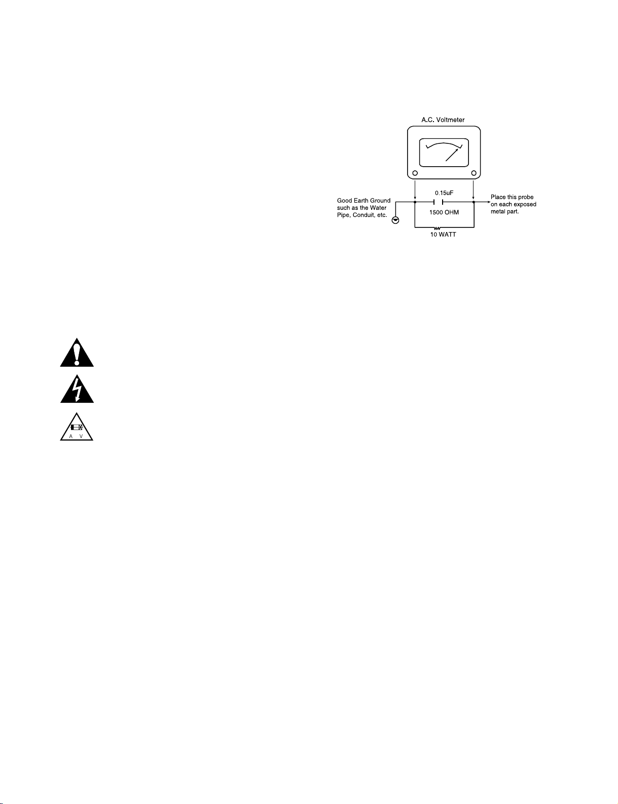
6. After reassembly of the set, always perform an AC leakage test on all exposed
metallic parts of the cabinet (the channel selector knobs, antenna terminals,
handle and screws) to be sure that set is safe to operate without danger of
electrical shock. DO NOT USE A LINE ISOLATION TRANSFORMER DURING
THIS TEST. Use an AC voltmeter having 5000 ohms per volt or more sensitivity
in the following manner: Connect a 1500 ohm, 10 watt resistor, paralleled by a .15
mfd 150V AC type capacitor between a known good earth ground water pipe,
conduit, etc.) and the exposed metallic parts, one at a time. Measure the AC
voltage across the combination of 1500 ohm resistor and .15 mfd capacitor.
Reverse the AC plug by using a non-polarized adaptor and repeat AC voltage
measurements for each exposed metallic part. Voltage measured must not
exceed 0.75 volts RMS. This corresponds to 0.5 milliamp AC. Any value
exceeding this limit constitutes a potential shock hazard and must be corrected
immediately.
TIPS ON PROPER INSTALLATION
1. Never install any receiver in a closed-in recess, cubbyhole, or closely fitting shelf
space over, or close to, a heat duct, or in the path of heated air flow.
2. Avoid conditions of high humidity such as: outdoor patio installations where dew
is a factor, near steam radiators where steam leakage is a factor, etc.
3. Avoid placement where draperies may obstruct venting. The customer should also
avoid the use of decorative scarves or other coverings that might obstruct
ventilation.
4. Wall- and shelf-mounted installations using a commercial mounting kit must follow
the factory-approved mounting instructions. A product mounted to a shelf or
platform must retain its original feet (or the equivalent thickness in spacers) to
provide adequate air flow across the bottom. Bolts or screws used for fasteners
must not touch any parts or wiring. Perform leakage tests on customized
installations.
5. Caution customers against mounting a product on a sloping shelf or in a tilted
position, unless the receiver is properly secured.
6. A product on a roll-about cart should be stable in its mounting to the cart.
Caution the customer on the hazards of trying to roll a cart with small casters
across thresholds or deep pile carpets.
7. Caution customers against using extension cords. Explain that a forest of
extensions, sprouting from a single outlet, can lead to disastrous consequences to
home and family.
Page 5

1-4
SERVICING PRECAUTIONS
CAUTION: Before servicing the Super Multi Blue Player
covered by this service data and its supplements and
addends, read and follow the SAFETY PRECAUTIONS.
NOTE: if unforeseen circumstances create conflict between
the following servicing precautions and any of the safety
precautions in this publications, always follow the safety
precautions.
Remember Safety First :
General Servicing Precautions
1.Always unplug the Super Multi Blue Player AC power cord
from the AC power source before:
(1) Removing or reinstalling any component, circuit board,
module, or any other assembly.
(2) Disconnecting or reconnecting any internal electrical
plug or other electrical connection.
(3) Connecting a test substitute in parallel with an
electrolytic capacitor.
Caution : A wrong part substitution or incorrect polarity
installation of electrolytic capacitors may result in an
explosion hazard.
2.Do not spray chemicals on or near this Super Multi Blue
Player or any of its assemblies.
3.Unless specified otherwise in this service data, clean
electrical contacts by applying an appropriate contact
cleaning solution to the contacts with a pipe cleaner,
cotton-tipped swab, or comparable soft applicator.
Unless specified otherwise in this service data, lubrication
of contacts is not required.
4.Do not defeat any plug/socket B+ voltage interlocks with
whitch instruments covered by this service manual might
be equipped.
5.Do not apply AC power to this Super Multi Blue Player and
/ or any of its electrical assemblies unless all solidstate
device heat sinks are correctly installed.
6.Always connect the test instrument ground lead to an
appropriate ground before connecting the test instrument
positive lead. Always remove the test instrument ground
lead last.
Insulation Checking Procedure
Disconnect the attachment plug from the AC outlet and turn
the power on. Connect an insulation resistance meter (500V)
to the blades of the attachment plug. The insulation
resistance between each blade of the attachment plug and
accessible conductive parts (Note 1) should be more than
1Mohm.
Note 1 : Accessible Conductive Parts include Metal panels,
Input terminals, Earphone jacks,etc.
Electrostatically Sensitive (ES) Devices
Some semiconductor (solid state) devices can be damaged
easily by static electricity. Such components commonly are
called Electrostatically Sensitive (ES) Devices. Examples of
typical ES devices are integrated circuits and some field
effect transistors and semiconductor chip components.
The following techniques should be used to help reduce the
incidence of component damage caused by static electricity.
1.Immediately before handling any semiconductor
component or semiconductor-equipped assembly, drain off
any electrostatic charge on your body by touching a known
earth ground. Alternatively, obtain and wear a
commercially available discharging wrist strap device,
which should be removed for potential shock reasons prior
to applying power to the unit under test.
2.After removing an electrical assembly equipped with ES
devices, place the assembly on a conductive surface such
as aluminum foil, to prevent electrostatic charge buildup or
exposure of the assembly.
3.Use only a grounded-tip soldering iron to solder or
unsolder ES devices.
4.Use only an anti-static solder removal device. Some solder
removal devices not classified as “anti-static” can generate
electrical charges sufficient to damage ES devices.
5.Do not use freon-propelled chemicals. These can generate
an electrical charge sufficient to damage ES devices.
6.Do not remove a replacement ES device from its
protective package until immediately before you are ready
to install it. (Most replacement ES devices are packaged
with leads electrically shorted together by conductive
foam, aluminum foil,or comparable conductive material).
7.Immediately before removing the protective material from
the leads of a replacement ES device, touch the protective
material to the chassis or circuit assembly into which the
device will be installed.
Caution: Be sure no power is applied to the chassis or
circuit, and observe all other safety precautions.
8.Minimize bodily motions when handling unpackaged
replacement ES devices. (Normally harmless motion such
as the brushing together of your clothes fabric or the lifting
of your foot from a carpeted floor can generate static
electricity sufficient to damage an ES device.)
Page 6
1-5
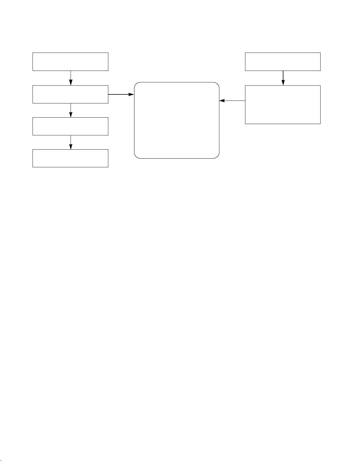
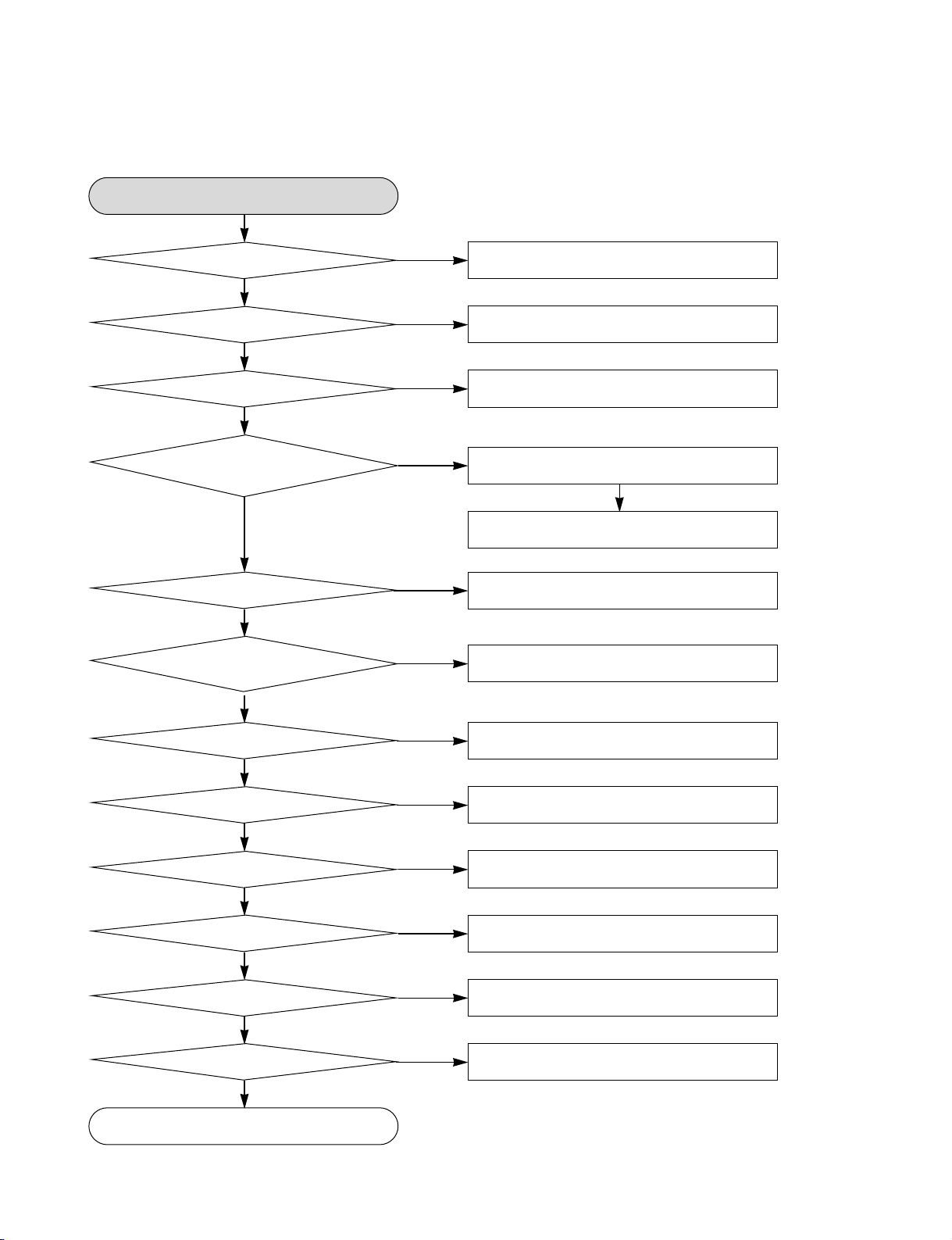
SERVICE INFORMATION FOR EEPROM IC SETTING
Option data read
YES
EEPROM ID check
(Whether a filename of
“eepromif.txt” exists or not)
YES
YES
Check the player set is
“No Disc” or “STOP” state.
Press the “PAUSE” key
and also press orderly
“1472” of number key.
Program start
*** EEPROM initial ***
- Check the player set is “No Disc” or “OPEN” state.
Move hightlight to SETUP --> Display --> TV Aspect --> 16:9 Wide.
And press orderly “1397139” + “ENTER” key of remocon.
Option confirmation mode
MICOM normal
operation start
NO
NO
EEPROM edit table
00 00 00 00 00 00 00 00
UP/DOWN key : Change the
EEPROM data
LEFT/RIGHT key : Move the
Cursor
PAUSE key : Store the
changeddata and
Exit the EEPROM
Edit Table
Detect new EEPROM
(Option edit screen)
Page 7

1-6
•Burn a DVD recordable disc using UDF format with a file that is named to “LG_BH_LX100000BN.ROM”.
• Insert a upgrading disc that was burned to UDF format only.
• Show help message for disc upgrade as follows.
<in the case of Back End Only or Front End Only burned on DISC>
Firmware Upgrade Mode [Back End]
Current Version : Vxxx.xx
New Version : Vxxx.xx
Press “PLAY” key to upgrade.
• Press play key to upgrade and it will show progress information
(Display percent[%] at VFD panel)
• After completing upgrade then it re-boot by auto.
Firmware Upgrade Mode [Back End]
Current Version : Vxxx.xx
New Version : Vxxx.xx
Upgrading ... Please Wait !!!
DISC UPGRADE
Page 8

1-7
SPECIFICATIONS
• GENERAL
Power requirements : AC 200-240V, 50/60Hz
Power consumption : 30W
Dimensions (W x H x D) : Approx. 430 x 78 x 250 mm (17 x 3.1 x 9.9 inches) without foot
Weight (Approx.) : 4.1kg (9.1 lbs)
Operating temperature : 5°C to 35°C (41°F to 95°F)
Operating humidity : 5% to 90%
• OUTPUTS
VIDEO OUT : 1.0V (p-p), 75Ω, sync negative, RCA jack x 1/SCART(TO TV)
COMPONENT VIDEO OUT : (Y) 1.0V (p-p), 75Ω,negative sync, RCA jack x 1
(Pb)/(Pr) 0.7V (p-p), 75Ω, RCA jack x 2
HDMI OUT (video/audio) : 19pin (HDMI standard, Type A)
ANALOG AUDIO OUT : 2CH : 2.0Vrms (1kHz, 0dB), 600Ω, RCA jack (L, R) x 1/SCART(TO TV)
6CH : 2.0Vrms (1kHz, 0dB), 600Ω, RCA jack x 6
DIGITAL OUT (COAXIAL) : 0.5V (p-p), 75Ω, RCA jack x 1
DIGITAL OUT (OPTICAL) : 3V (p-p), 75Ω, Optical jack x 1
• SYSTEM
Laser : Semiconductor laser, wavelength : 405nm/650nm/780nm
Signal system : Standard NTSC Color TV system
Frequency response : 8Hz to 44kHz (96 kHz Sampling)
8Hz to 22kHz (48 kHz Sampling)
Signal-to-noise ratio : More than 100dB (ANALOG OUT connectors only)
Harmonic distortion : Less than 0.008%
Dynamic range : More than 95dB
Accessories : Video cable (1), Audio cable (1), Remote control (1), Batteries (2)
Note : Design and specifications are subject to change prior notice.
Page 9

2-1
SECTION 2
CABINET & MAIN CHASSIS
CONTENTS
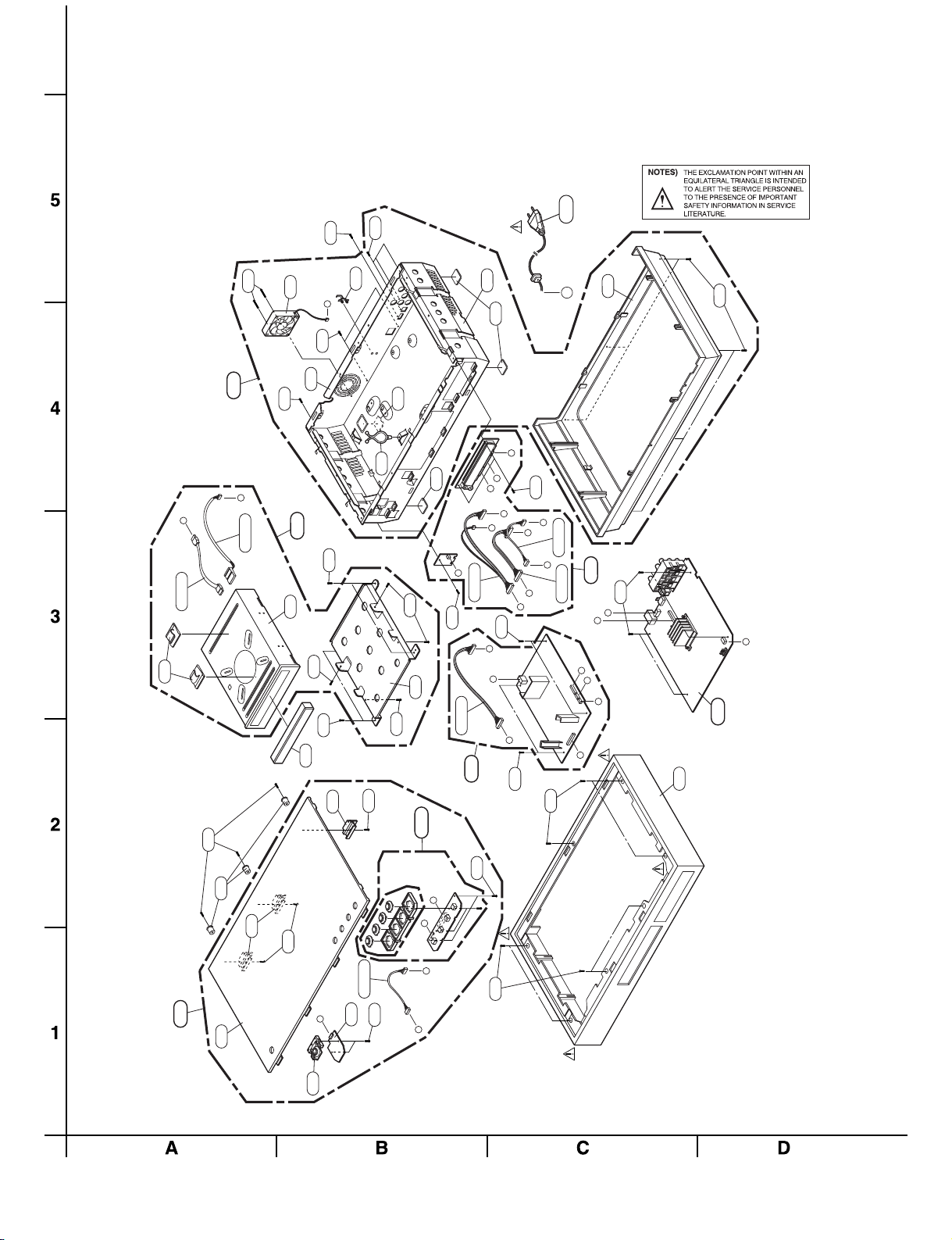
EXPLODED VIEWS .....................................................................................................................................2-2
1. CABINET AND MAIN FRAME SECTION ..................................................................................................2-2
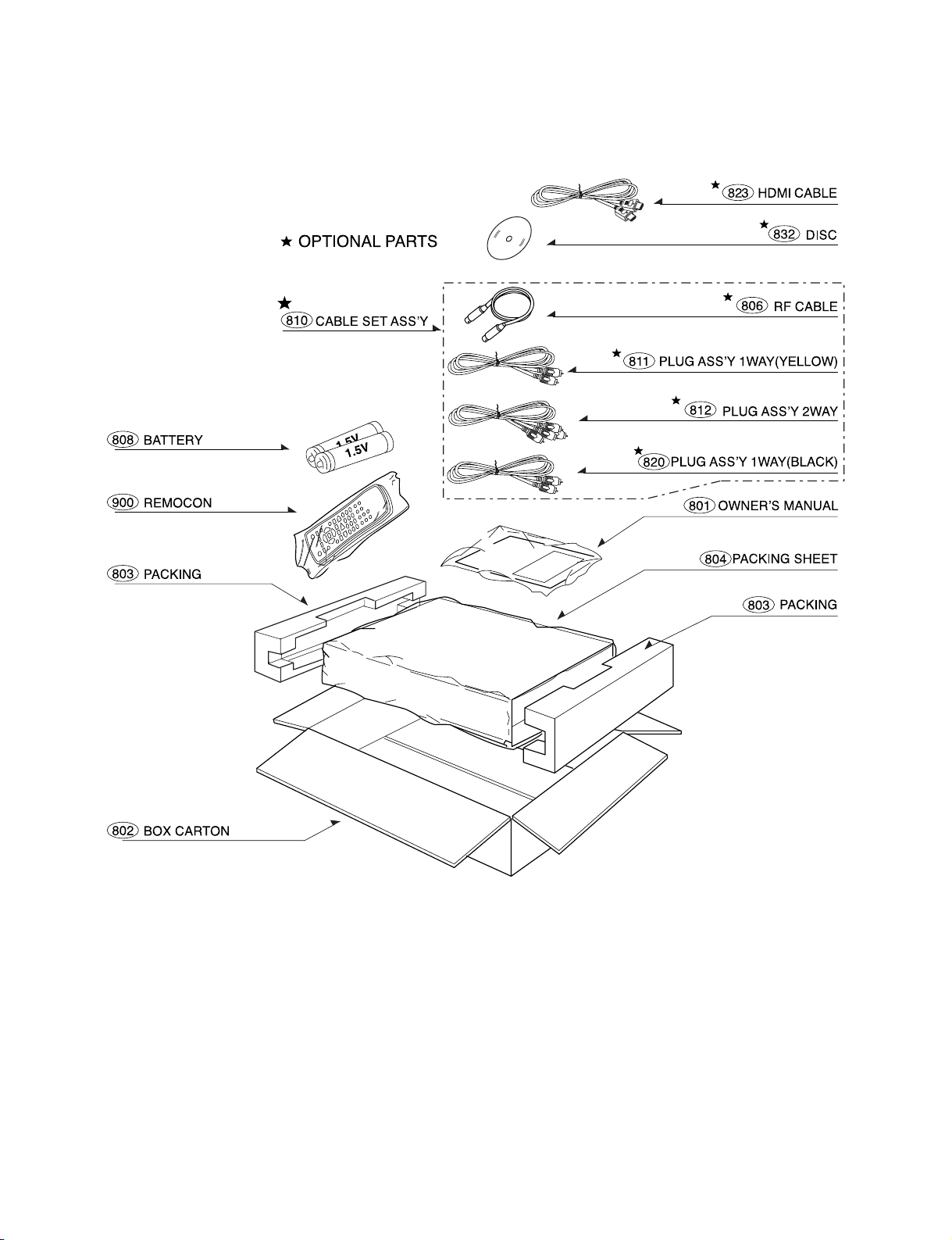
2. PACKING ACCESSORY SECTION...........................................................................................................2-3
Page 10
A
P
C
Q
E
R
P
B
J
D
R
G
K
G
H
J
Q
H
K
F
L
F
E
M
L
D
C
B
A
280
A43
284
286
469
283
253
468
330
260
465
320
265
267
467
465
465
465
466
468
468
468
261
261
261
468
468
285
468
A60
A44
A47
A50
A46
254
252
283
469
263
465
469
469
469
465
469
A43A
CABLE1
CABLE6
CABLE7
CABLE5
CABLE4
CABLE3
CABLE2
469
465
279
262
FRONT
BOARD
SMPS
BOARD
MAIN
BOARD
2-2
EXPLODED VIEWS
1. CABINET AND MAIN FRAME SECTION
M
300
Page 11
2-3
2. PACKING ACCESSORY SECTION
Page 12

3-1
SECTION 3
ELECTRICAL
CONTENTS
ELECTRICAL TROUBLESHOOTING GUIDE.....................................................................................3-2
1. POWER SUPPLY (SMPS).....................................................................................................................3-2
2. POWER ON ...........................................................................................................................................3-5
3. SYSTEM PART......................................................................................................................................3-6
4. VIDEO PART (COMMON) .....................................................................................................................3-7
5. COMPONENT (YPbPr) VIDEO OUT.....................................................................................................3-8
6. CVBS VIDEO OUT ................................................................................................................................3-9
7. AUDIO (ANALOG) ...............................................................................................................................3-10
8. AUDIO (S/PDIF) ...................................................................................................................................3-11
9. HDMI....................................................................................................................................................3-12
WAVEFORMS ..............................................................................................................................................3-13
1.SYSTEM PART-1..................................................................................................................................3-13
2.SYSTEM PART-2 (SYSTEM MEMORY) ..............................................................................................3-14
3.VIDEO PART-1 (100% FULL COLOR-BAR).........................................................................................3-15
4.VIDEO PART-2 (100% FULL COLOR-BAR).........................................................................................3-16
5.AUDIO PART-1 (ANALOG 5CH : 99Hz, -20dBFS / WOOFER : 30Hz, 0dBFS)...................................3-17
6.AUDIO PART-2 (S/PDIF) ......................................................................................................................3-18
7.HDMI PART...........................................................................................................................................3-19
8.FRONT I/F PART ..................................................................................................................................3-20
9.MPEG-4 DECODER PART-1................................................................................................................3-21
10.MPEG-4 DECODER PART-2................................................................................................................3-22
BLOCK DIAGRAMS ..................................................................................................................................3-23
1.OVERALL BLOCK DIAGRAM ..............................................................................................................3-23
2.SIGNAL PATH BLOCK DIAGRAM........................................................................................................3-24
3.WIRING BLOCK DIAGRAM..................................................................................................................3-25
4.FRONT BLOCK DIAGRAM...................................................................................................................3-26
5.SMPS BLOCK DIAGRAM.....................................................................................................................3-27
CIRCUIT DIAGRAMS................................................................................................................................3-29
1. SMPS (POWER) CIRCUIT DIAGRAM ................................................................................................3-29
2. DECODER-1 CIRCUIT DIAGRAM ......................................................................................................3-31
3. DECODER-2 CIRCUIT DIAGRAM ......................................................................................................3-33
4. MPEG-1 CIRCUIT DIAGRAM..............................................................................................................3-35
5. MPEG-2 CIRCUIT DIAGRAM..............................................................................................................3-37
6. 512MB SDRAM CIRCUIT DIAGRAM ..................................................................................................3-39
7. ROM, IDE, ETHERNET JTAG, UART, FP I/F CIRCUIT DIAGRAM ....................................................3-41
8. AUDIO FPGA CIRCUIT DIAGRAM......................................................................................................3-43
9. AUDIO & VIDEO CIRCUIT DIAGRAM.................................................................................................3-45
10. POWER CIRCUIT DIAGRAM..............................................................................................................3-47
11. FRONT/TIMER CIRCUIT DIAGRAM ...................................................................................................3-49
12. LOGO CIRCUIT DIAGRAM .................................................................................................................3-51
CIRCUIT VOLTAGE CHART...................................................................................................................3-53
PRINTED CIRCUIT DIAGRAMS............................................................................................................3-55
1. MAIN P.C.BOARD..................................................................................................................................3-55
2. FRONT P.C.BOARD ..............................................................................................................................3-57
3. LOGO P.C.BOARD ................................................................................................................................3-58
4. POWER P.C.BOARD.............................................................................................................................3-59
Page 13
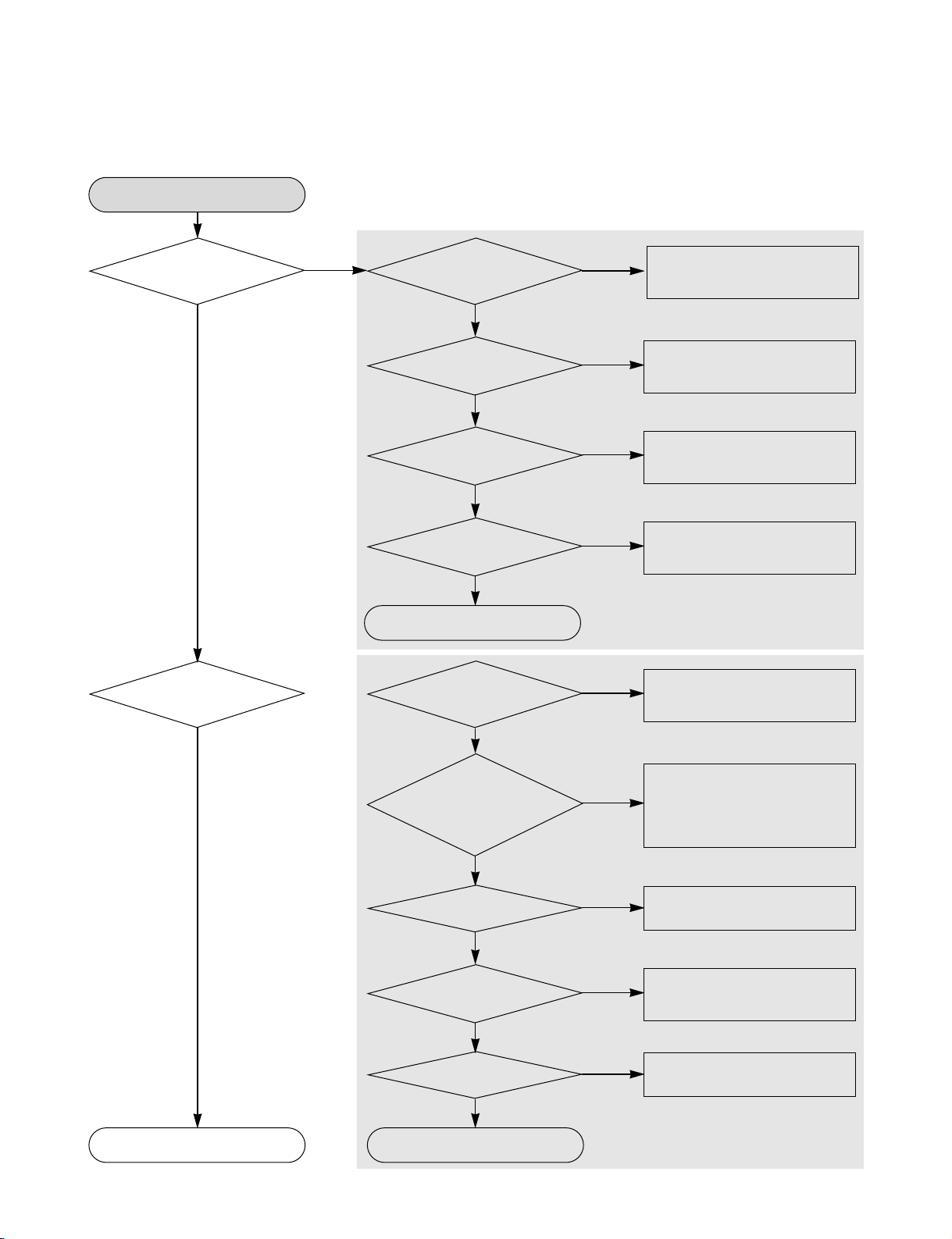
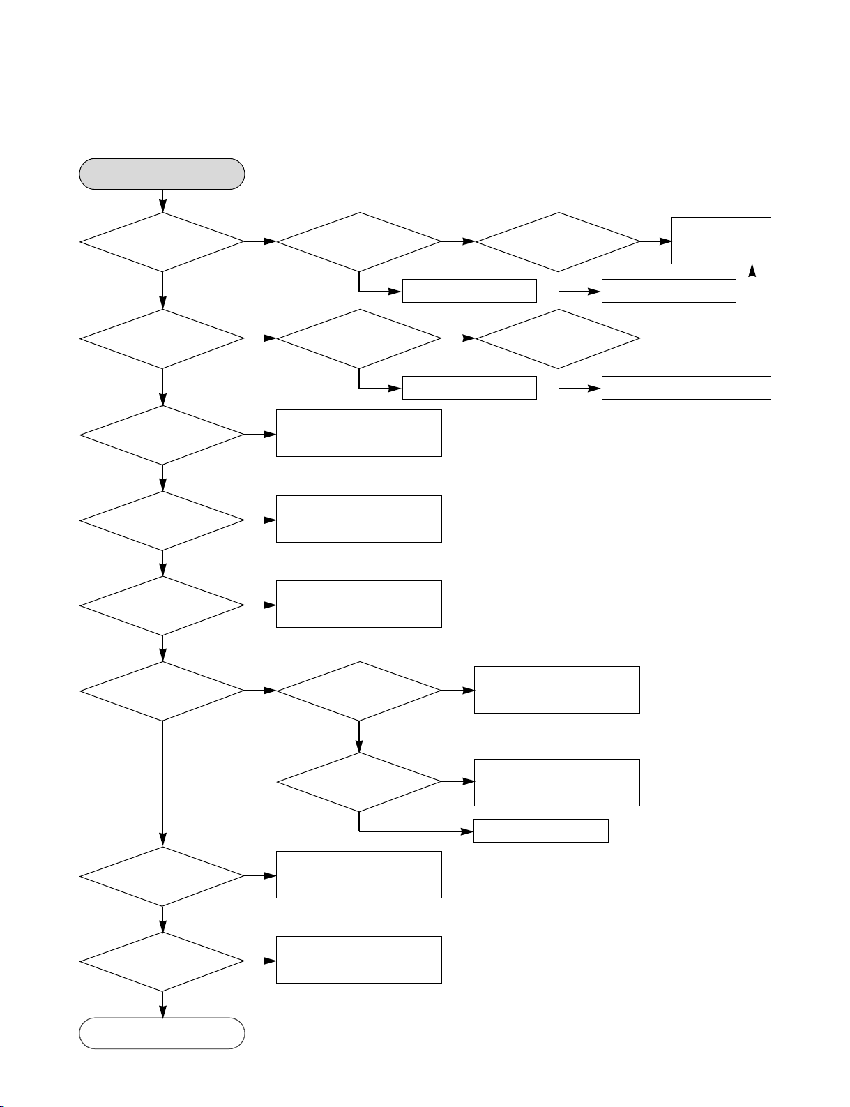
Is the D121 normal?
3-2
ELECTRICAL TROUBLESHOOTING GUIDE
1. POWER SUPPLY (SMPS)
No .5.3VA
YES
Is the F101 normal? Replace the F101 (Use the same fuse)
YES
NO
Is the BD101 normal? Replace the BD101
YES
NO
Is the R101 normal? Replace the R101
YES
NO
Is Vcc (9V - 18V) supplied
to IC101 Pin2?
Is the D102 normal?
YES
NO
NO
Check or replace the D102
IS the D123 normal? Replace the D123
YES
NO
Is there about 2.5V
at the IC103 Pin1?
Replace the IC103
YES
NO
Is the IC102 normal? Replace the IC102
YES
NO
Is the D124 normal? Replace the D124
YES
NO
Is the D127 normal? Replace the D127
YES
NO
Is the D128 normal? Replace the D128
YES
NO
Replace the D121
YES
NO
Is the D122 normal? Replace the D122
YES
NO
Power line of main PCB is short
Page 14
3-3
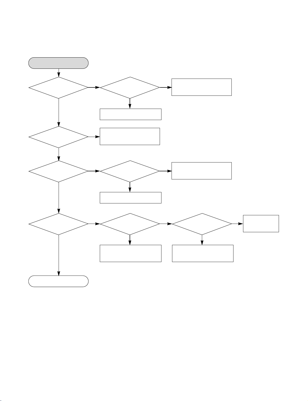
ELECTRICAL TROUBLESHOOTING GUIDE
No 5.0 Loader
Is the Vcc
(5.3V) supplied to
IC156 Pin1?
Check or Replace the D128
YES
NO
NO
Is the IC156 pin4 “H”?
Check the PWR CTL
“H” signal from µ-com
YES
Check or replace the IC156
No 3.3V
Is the Vcc
(3.8V) supplied to
IC153 Pin1?
Check or replace the D127
YES
NO
NO
Is the IC153 Pin4 “H”?
Check the PWR CTL
“H” signal from µ-com
YES
Check or replace the IC153
No 12V (Main)
Is the Vcc
(13.5V) supplied to
IC152 Pin1?
Check or replace the D124
YES
NO
NO
Is the IC152 Pin4 ‘H’?
Check the PWR CTL
“H” signal from µ-com
YES
Check or replace the IC152
Page 15
3-4
No 12 (Fan, Loader)
Is the Vcc
(13.5V) supplied to
IC155 Pin1?
Check or replace the D124
YES
NO
NO
Is the IC155 Pin4 “H”?
Check the PWR CTL
“H” signal from µ-com
YES
Check or replace the IC155
No VF+
Is the ZD121 normal?
Replace the ZD121
YES
NO
Replace the R121
ELECTRICAL TROUBLESHOOTING GUIDE
Page 16
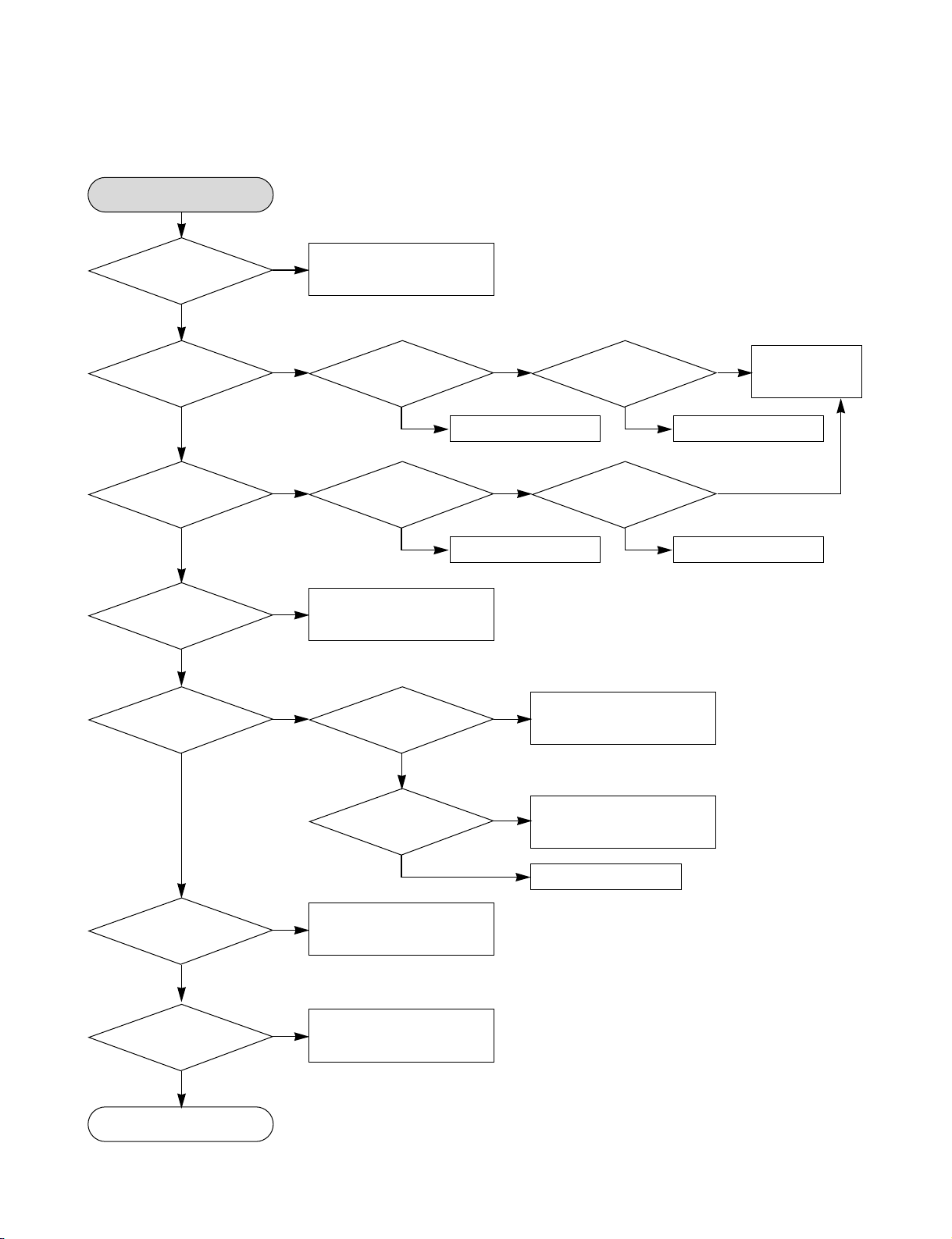
3-5
POWER on
Normal TV
function OK
Front I/F cable connect
"HELLO PLEASE WAIT"
Display on VFD OK?
Front I/F
cable connection
OK?
NO
NO
YES
VFD power cable connect
VFD power
cable connection
OK?
NO
YES
YES
YES
YES
Touch-Pad I/F
cable connect
"LED ON"
on Touch-Pad OK?
Touch-Pad I/F
cable connection OK?
NO NO
YES
Proper display
cable connect
"LG LOGO"
display on monitor OK?
Display
cable connection
OK?
NO NO
YES
2. POWER ON
ELECTRICAL TROUBLESHOOTING GUIDE
Page 17
3-6
POWER on
Main Board
Timer Board
Check SMPS
"HELLO PLEASE WAIT"
Display on VFD OK?
P602, 8 pin; +5V,
3 pin; -28V, 4 pin; -32V,
5 pin; -36V ?
NO
NO
YES
YES
YES
X602 change
X602 10MHz OK?
NO
YES
IC600 change
R613 About 625kHz
serial Clock OK?
NO
YES
IC601 change
R611
about 3MHz
OK?
NO
YES
DIS600 change
Check SMPS
“READING”
Display on VFD OK?
P901,
11pin; 12V, 9 pin; 5V,
4 pin; 3.3V?
YES
IC904 Change,
IC901 Change
IC905 or IC903 or
IC908 Change, IC907
Change, IC902
C971; 2.6V,
C972 ; 1.3V C962, C967,
C9F5 ; 1.2V, C9F3 ; 2.5V,
C9E3; 1.8V ?
NO
NO
YES
X402 change
X402
54.000MHz OK?
NO
X401 Change
X401
25.000MHz OK?
NO
YES
IC605 change
IC402
Pin 2, 3, 5, 7 27MHz
OK?
NO
YES
YES
Check IC301System part OK
3. SYSTEM PART
ELECTRICAL TROUBLESHOOTING GUIDE
Page 18
3-7
No display
Video part OK
C863
(Pin 2) +3.3V
OK?
IC907
(Pin 2) +3.3V
OK?
NO
P901
(Pin 3, 4) +3.3V
OK?
NO NO
YES
YES
YES
Check main
power cable
L803 Re-soldering
YES
L904, L906 Re-soldering
C327
(Pin 2) +2.5V
OK?
C970
(Pin 2) +2.6V
OK?
NO
IC904
(Pin 2) +5.0V
OK?
NO NO
YES
L304 Re-soldering
YES
IC904 Change
C968
(Pin 2) +1.2V
OK?
NO
IC903 Re-soldering
C8F9, C8G0,
C8G1, C8F6 (Pin 2)
signal OK?
L816, L811, L813,
L820 soldering OK?
NO NO
Re-soldering
Re-soldering
L812, L819, L815
soldering OK?
NO
YES
Check IC301
CF804,
CF802, CF806, CF803
(Pin 1) signal OK?
NO
C8F9 ~ C8F6
Re-soldering
YES
YES
YES
YES
JK803
(Pin 1, 3, 5, 7)
signal OK?
NO
CF804 ~ CF803
Re-soldering
YES
YES
VIDEO cable
connection
OK?
NO
Check VIDEO cable
4. VIDEO PART (COMMON)
ELECTRICAL TROUBLESHOOTING GUIDE
Page 19
3-8
Component video no display
Component video cable connect
YES
NO
5. COMPONENT (YPbPr) VIDEO OUT
Video cable
connection OK?
Video part (Common) check
YES
NO
TP782 ~ TP784 video
signal input OK?
Re-soldering
YES
NO
L812, L819, L815
soldering OK?
Re-soldering
YES
NO
L818, L814, L809
soldering OK?
Re-soldering
YES
NO
L811, L813, L820
soldering OK?
Re-soldering
YES
NO
C8G0, C8G1, C8F6
soldering OK?
Re-soldering
YES
NO
CF802, CF806, CF803
soldering OK?
Re-soldering
YES
NO
JK803 soldering OK?
Component Video OK
ELECTRICAL TROUBLESHOOTING GUIDE
Page 20
3-9
CVBS video no display
Composite cable connect
YES
NO
6. CVBS VIDEO OUT
Video cable
connection OK?
Video part (Common) check
YES
NO
TP871
Video signal input OK?
Re-soldering
YES
NO
C806 soldering OK?
Re-soldering
YES
NO
L816 soldering OK?
Re-soldering
YES
NO
C8F9 soldering OK?
Re-soldering
YES
NO
CF804 soldering OK?
Re-soldering
YES
NO
JK803 soldering OK?
CVBS video OK
ELECTRICAL TROUBLESHOOTING GUIDE
Page 21
3-10
No audio
Audio part OK
IC804 ~ IC806
(Pin 8) +11.5V
OK?
C9E7
(Pin 2) +12.0V
OK?
NO
P901
(Pin 11) +12.0V
OK?
NO NO
YES
YES
YES
Check main
power cable
R882 Re-soldering
YES
L905 Re-soldering
IC802
(Pin 28) +5.0V
OK?
C8F5
(Pin 2) +5.0V
OK?
NO
P901
(Pin 9, 8, 7) +5.0V
OK?
NO NO
YES
R855 Re-soldering
YES
L901 ~ 903 Re-soldering
R854, R839, R836
R878~R880 Soldering
OK?
NO
Re-soldering
TP847
LOW = GND
OK?
R884, R814
soldering OK?
NO NO
Re-soldering
Re-soldering
Q806
soldering OK?
NO
YES
Check IC701
C8E1 ~ C8E6
soldering
OK?
NO
Re-soldering
YES
IC802 (Pin 7, 8, 9)
I2S input signal
OK?
NO
Check IC701
YES
YES
YES
TP816 ~ TP821
audio out signal
OK?
NO
Check IC802
YES
YES
YES
JK803 (Pin 11 ~ 21)
audio out signal
OK?
NO
Change IC804 ~ 806
7. AUDIO (ANALOG)
ELECTRICAL TROUBLESHOOTING GUIDE
Page 22
3-11
No audio
S/PDIF audio OK
IC801
(Pin 5) +3.3V
OK?
P901
(Pin 3,4) +3.3V
OK?
NO NO
YES
YES
YES
YES
Check IC301
main power cable
Check main
power cable
L904, L906 Re-soldering
Change IC801
YES
Change JK802
YES
L901 ~ L903
Re-soldering
IC801 (Pin 4)
Digital Audio Out
OK?
IC801
soldering OK?
NO NO
YES
Re-soldering
JK802
Red Lighting
OK?
JK802
(Pin 2) +5.0V
OK?
NO NO
NO
P901
(Pin 9, 8, 7) +5.0V
OK?
TP8A0
digital audio input
OK?
NO
Check IC301
YES
8. AUDIO (S/PDIF)
ELECTRICAL TROUBLESHOOTING GUIDE
Page 23
3-12
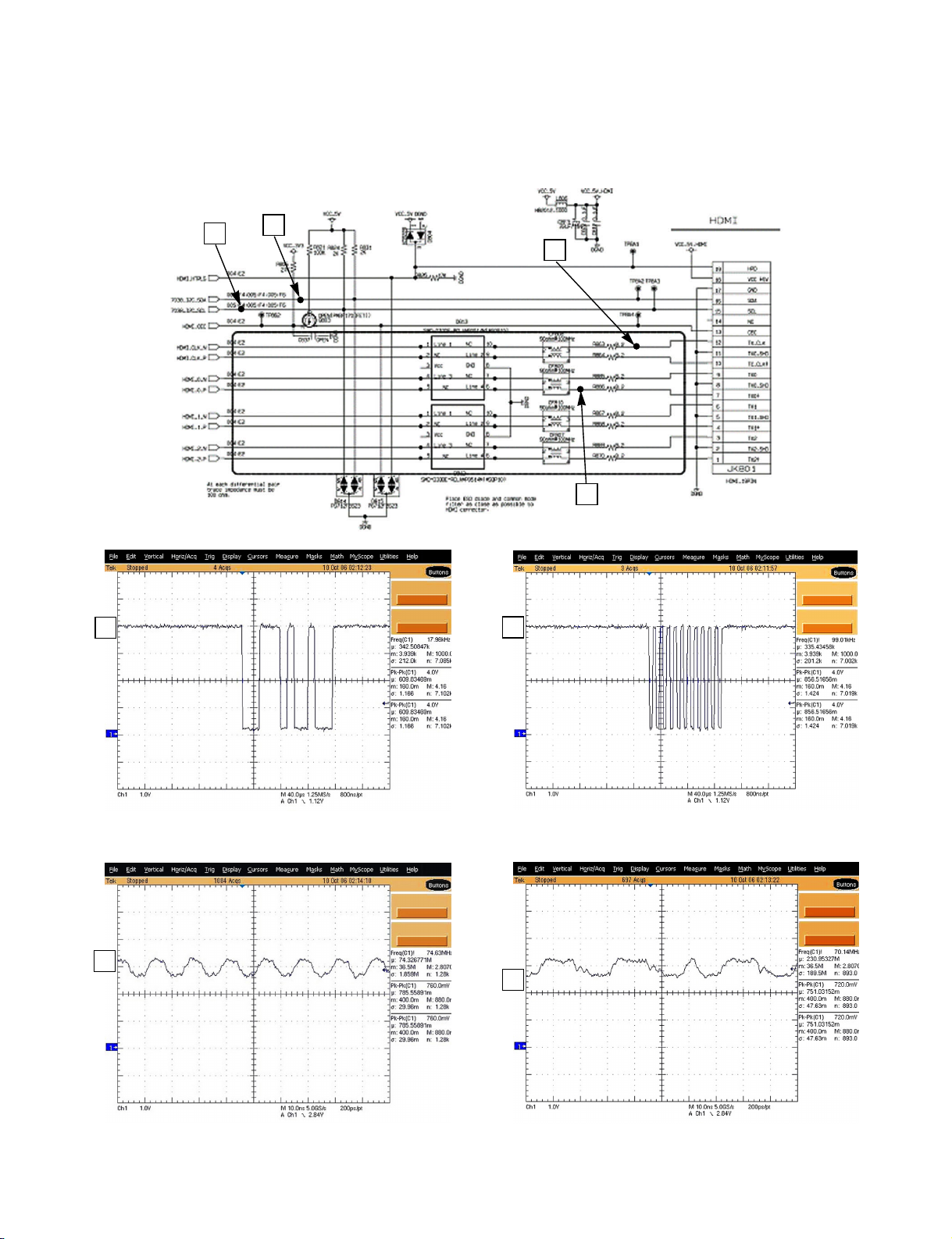
No A/V
HDMI OK
JK801
Pin 19 (HPD)
OK?
NO
YES
Check IC301
JK801
Pin 15 (SCL), 16 (SDA)
OK?
NO
YES
Check IC301
Check IC301
JK801
Pin 18 +5V
OK?
NO
P901 Pin 7, 8, 9 Check
NO
Re-soldering
YES
JK801
Pin 1, 3, 4, 6, 7, 9, 10,
12 OK?
NO
NO
Re-soldering
YES
Check
CF807~810
OK?
YES
9. HDMI
ELECTRICAL TROUBLESHOOTING GUIDE
Page 24
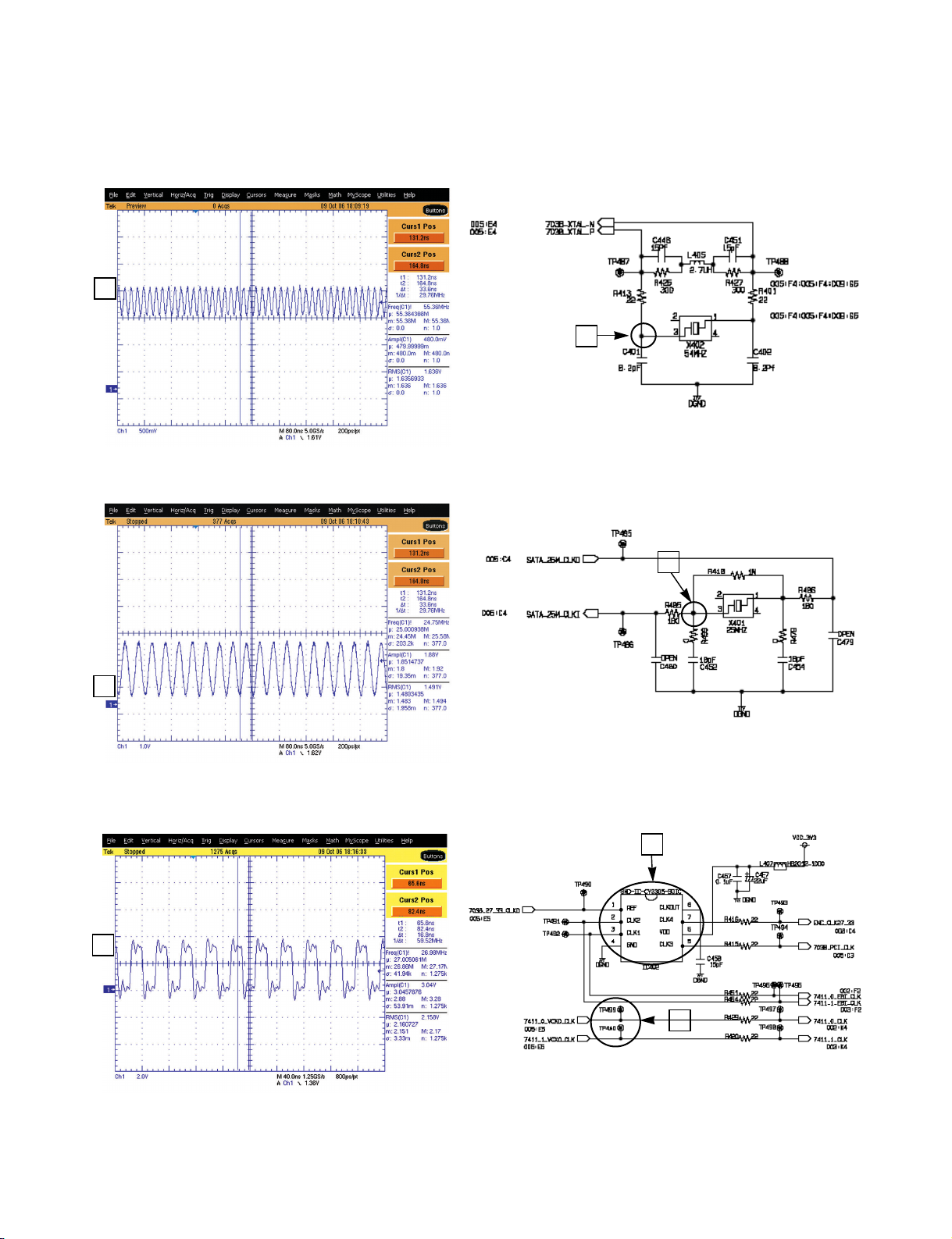
3-13
WAVEFORMS
1. SYSTEM PART-1
7438 XTAL (54MHz)
1
1
7438 XTAL for SATA loader (25MHz)
2
2
7438 CLK(27MHz), 7438 PCI CLK(27MHz)
7438 FPGA CLK(27MHz), 7412_0 CLK(27MHz)
7412_1 CLK(27MHz)
3
3
3
Page 25

3-14
2. SYSTEM PART-2 (SYSTEM MEMORY)
4
4
7438 DDR BA0
5
7
6
5
7438 DDR WE
6
7438 DDR CAS
7
7438 DDR CLK0 (200MHz)
Page 26
3-15
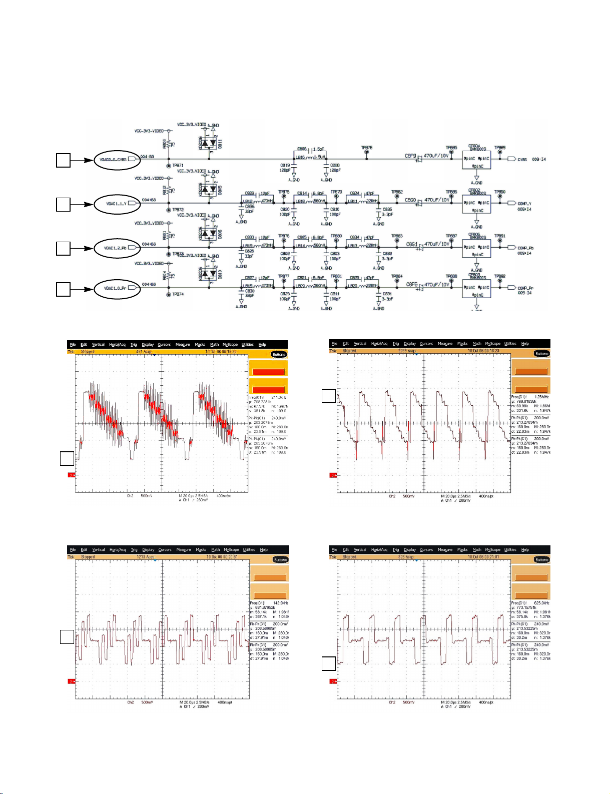
3. VIDEO PART-1 (100% FULL COLOR-BAR)
8
9
10
11
10
VDAC1_2_Pb
11
VDAC1_0_Pr
8
VDAC0_0_CVBS
9
VDAC1_1_Y
Page 27
3-16
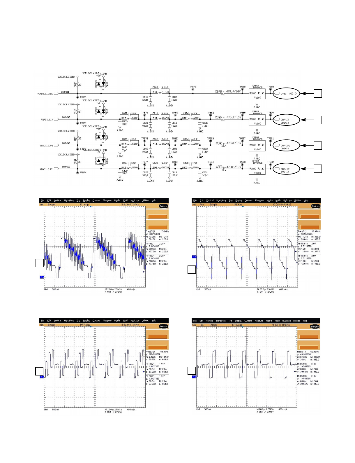
4. VIDEO PART-2 (100% FULL COLOR-BAR)
12
13
14
15
14
COMP_Pb
15
COMP_Pr
12
CVBS
13
COMP_Y
Page 28
3-17
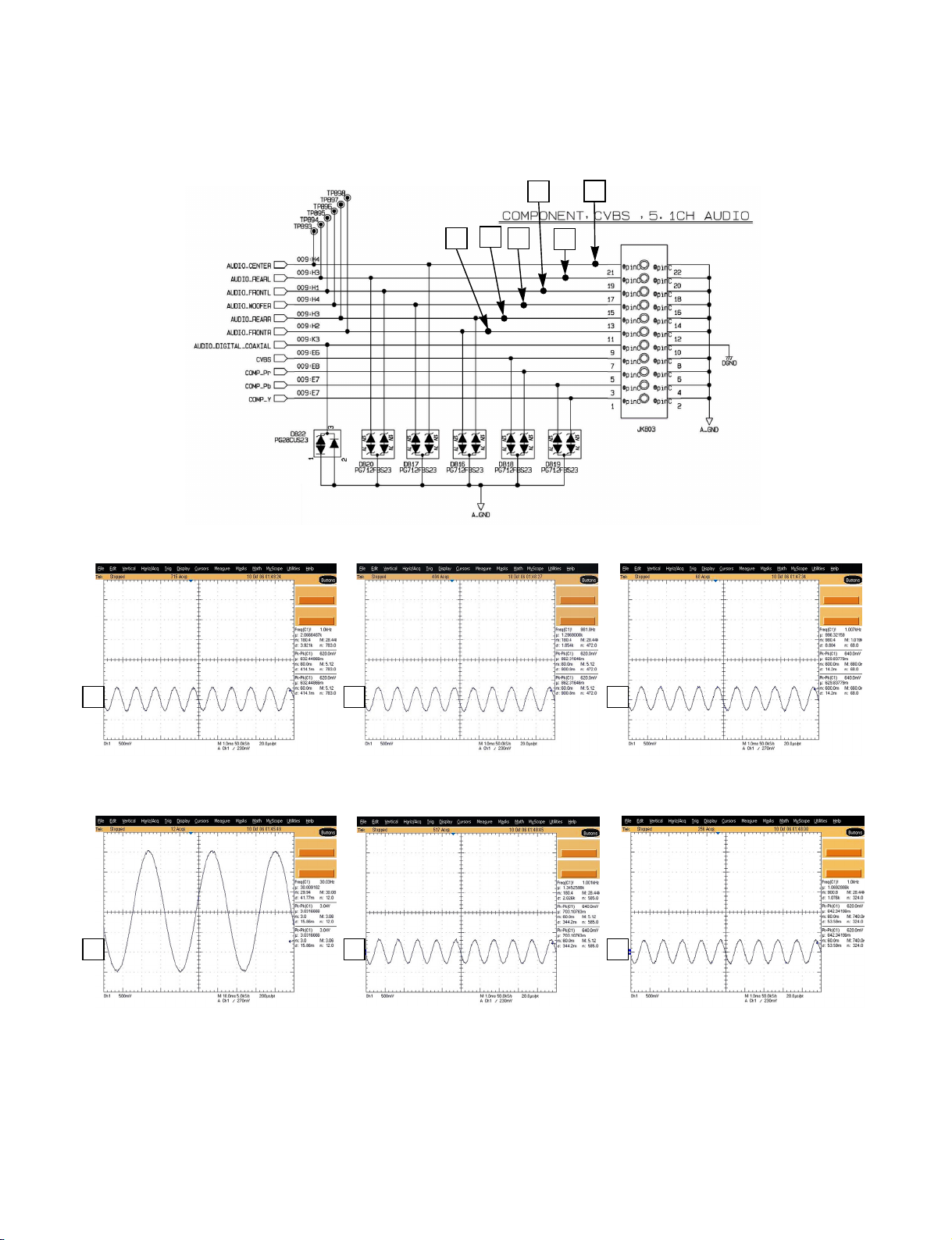
5. AUDIO PART-1 (ANALOG 5CH : 99Hz, -20dBFS / WOOFER : 30Hz, 0dBFS)
21
20
19
18
17
16
16
AUDIO_CENTER
17
AUDIO_REARL
18
AUDIO_FRONTL
19
AUDIO_WOOFER
20
AUDIO_REARR
21
AUDIO_FRONTR
Page 29
3-18
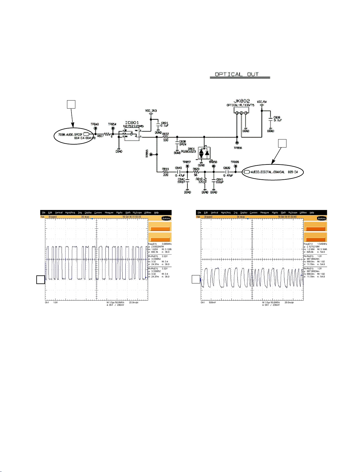
6. AUDIO PART-2 (S/PDIF)
22
23
22
7038_AUDIO_SPDIF
23
AUDIO_DIGITAL_COAXIAL
Page 30
3-19
7. HDMI PART
25
26
HDMI_CLK
27
HDMI_DATA
24
7038_I2C_SDA
25
7038_I2C_SCL
24
26
27
Page 31

3-20
8. FRONT I/F PART
28
29
28
UART_TXD
29
UART_RXD
Page 32

3-21
9. MPEG-4 DECODER PART-1
32
7412 DDR CLK (200MHz)
33
7412 DDR WE
30
7412 DDR BAO
31
7412 DDR CAS
33
30
32
31
Page 33

3-22
10. MPEG-4 DECODER PART-2
36
7412_O I2S_DATAO
37
7412_O_I2S_CLKO
34
7412_HD_DVIO_CLK (74.25MHz)
35
7412_O_I2S_LRCLKO
34
35
36
37
Page 34

3-23
BLOCK DIAGRAMS
1. OVERALL BLOCK DIAGRAM
Page 35

3-24
2. SIGNAL PATH BLOCK DIAGRAM
Page 36

3-25
3. WIRING BLOCK DIAGRAM
Page 37

3-26
4. FRONT BLOCK DIAGRAM
Page 38

3-27
5. SMPS BLOCK DIAGRAM
Page 39

3-28
MEMO
Page 40

3-29 3-30
CIRCUIT DIAGRAMS
1. SMPS (POWER) CIRCUIT DIAGRAM
WHEN SERVICING THIS CHASSIS, UNDER NO
CIRCUMSTANCES SHOULD THE ORIGINAL DESIGN
BE MODIFIED OR ALTERED WITHOUT PERMISSION
FROM THE LG CORPORATION. ALL COMPONENTS
SHOULD BE REPLACED ONLY WITH TYPES
IDENTICAL TO THOSE IN THE ORIGINAL CIRCUIT.
SPECIAL COMPONENTS ARE SHADED ON THE
SCHEMATIC FOR EASY IDENTIFICATION. THIS
CIRCUIT DIAGRAM MAY OCCASIONALLY DIFFER
FROM THE ACTUAL CIRCUIT USED. THIS WAY,
IMPLEMENTATION OF THE LATEST SAFETY AND
PERFORMANCE IMPROVEMENT CHANGES INTO
THE SET IS NOT DELAYED UNTILTHE NEW SERVICE
LITERATURE IS PRINTED.
1. Shaded( ) parts are critical for safety. Replace only
with specified part number.
2. Voltages are DC-measured with a digital voltmeter
during Play mode.
IMPORTANT SAFETY NOTE :
Page 41

3-31 3-32
2. DECODER-1 CIRCUIT DIAGRAM
Page 42

3-33 3-34
3. DECODER-2 CIRCUIT DIAGRAM
Page 43

3-35 3-36
4. MPEG-1 CIRCUIT DIAGRAM
Page 44

3-37 3-38
5. MPEG-2 CIRCUIT DIAGRAM
Page 45

3-39 3-40
6. 512MB SDRAM CIRCUIT DIAGRAM
Page 46

3-41 3-42
7. ROM, IDE, ETHERNET JTAG, UART, FP I/F CIRCUIT DIAGRAM
Page 47

3-43 3-44
8. AUDIO FPGA CIRCUIT DIAGRAM
Page 48

3-45 3-46
9. AUDIO & VIDEO CIRCUIT DIAGRAM
Page 49

3-47 3-48
10. POWER CIRCUIT DIAGRAM
Page 50

3-49 3-50
11. FRONT/TIMER CIRCUIT DIAGRAM
Page 51

3-51 3-52
12. LOGO CIRCUIT DIAGRAM
Page 52

3-53 3-54
CIRCUIT VOLTAGE CHART
ALUMINUM CAPACITOR -1 : BY-PASS CAPACITOR
CAPACITOR VOLTAGE MEASUREMENT ON BH100 (VOLT)
NO LOC SPEC
EE MODE PLAYBACK
(+) (-) (+) (-)
1 C8E5 10uF/16V 5.48 0.90 5.48 1.10
2 C8E6 10uF/16V 5.47 1.30 5.47 0.50
3 C8E4 10uF/16V 5.46 0.00 5.42 1.40
4 C8E2 10uF/16V 5.44 0.00 5.46 0.60
5 C8E3 10uF/16V 5.46 0.00 5.45 0.60
6 C8E1 10uF/16V 5.44 1.60 5.43 0.50
7 C8G3 10uF/16V 2.22 0.00 2.20 0.00
8 C8F5 100uF/16V 4.83 0.00 4.80 0.00
9 C8F0 22uF/16V 10.65 0.00 10.65 0.00
10 C8F2 22uF/16V 10.65 0.00 10.65 0.00
11 C8F4 220uF/16V 11.87 0.00 11.87 0.00
12 C8G2 10uF/16V 4.42 0.00 4.42 0.00
13 C8E9 22uF/16V 3.18 0.00 3.18 0.00
14 C8G1 470uF/10V 1.92 0.00 1.80 0.00
15 C8G0 470uF/10V 1.92 0.00 1.13 0.00
16 C8F9 470uF/10V 1.12 1.05 1.27 1.12
17 C8F6 470uF/10V 1.75 0.00 1.77 0.00
18 C9E7 220uF/16V 11.87 0.00 11.87 0.00
19 C9E8 220uF/16V 4.83 0.00 4.83 0.00
20 C9F2 220uF/16V 3.18 0.00 3.18 0.00
21 C9F4 220uF/16V 11.87 0.00 11.87 0.00
22 C9E9 220uF/16V 4.83 0.00 4.81 0.00
23 C9F1 220uF/16V 3.18 0.00 3.18 0.00
24 C8F3 22uF/16V 4.83 0.00 4.82 0.00
25 C7E6 100uF/16V 3.18 0.00 3.18 0.00
26 C9E5 100uF/16V 3.18 0.00 3.18 0.00
27 C9F3 100uF/16V 2.55 0.00 2.55 0.00
28 C9E6 100uF/16V 2.55 0.00 2.55 0.00
29 C9F5 100uF/16V 1.25 0.00 1.25 0.00
30 C7E2 10uF/16V 2.55 0.00 2.55 0.00
31 C7E4 10uF/16V 1.25 0.00 1.25 0.00
32 C4E1 22uF/16V 3.18 0.00 3.18 0.00
33 C4E9 22uF/16V 3.18 0.00 3.18 0.00
34 C6E1 22uF/16V 3.18 0.00 3.18 0.00
35 C4E7 22uF/16V 3.17 0.00 3.17 0.00
36 C1E5 22uF/16V 3.18 0.00 3.18 0.00
38 C9E3 47uF/16V 1.81 0.00 1.81 0.00
40 C9E4 47uF/16V 3.18 0.00 3.18 0.00
41 C1E1 22uF/16V 1.16 0.00 1.16 0.00
42 C1E2 22uF/16V 1.13 0.00 1.13 0.00
NO LOC SPEC
EE MODE PLAYBACK
(+) (-) (+) (-)
43 C1E6 22uF/16V 1.15 0.00 1.15 0.00
44 C1E8 47uF/16V 1.18 0.00 1.18 0.00
45 C1E9 47uF/16V 1.18 0.00 1.18 0.00
46 C1E4 22uF/16V 2.57 0.00 2.57 0.00
47 C6E2 22uF/16V 4.82 0.00 4.82 0.00
48 C6E4 22uF/16V 4.82 0 4.82 0
49 C1E3 22uF/16V 2.57 0.00 2.57 0.00
50 C1E7 22uF/16V 2.57 0.00 2.57 0.00
51 C2E2 22uF/16V 2.57 0.00 2.57 0.00
52 C4E2 22uF/16V 3.18 0.00 3.18 0.00
53 C4F0 47uF/16V 3.18 0.00 3.18 0.00
54 C4E6 22uF/16V 1.17 0.00 1.17 0.00
55 C4E3 22uF/16V 1.18 0.00 1.18 0.00
56 C4F2 47uF/16V 1.18 0.00 1.18 0.00
57 C4E5 22uF/16V 1.18 0.00 1.18 0.00
58 C4E4 22uF/16V 1.18 0.00 1.18 0.00
59 C3E7 22uF/16V 1.29 0.00 1.29 0.00
60 C2E4 22uF/16V 3.12 0.00 3.12 0.00
61 C2E5 22uF/16V 1.16 0.00 1.16 0.00
62 C2E1 22uF/16V 1.13 0.00 1.13 0.00
63 C2E6 22uF/16V 1.14 0.00 1.14 0.00
64 C3E3 22uF/16V 2.58 0.00 2.58 0.00
65 C3E4 22uF/16V 1.17 0.00 1.17 0.00
66 C3E2 22uF/16V 1.18 0.00 1.18 0.00
67 C4E8 22uF/16V 2.58 0.00 2.58 0.00
68 C4F1 47uF/16V 2.58 0.00 2.58 0.00
69 C3E1 22uF/16V 1.29 0.00 1.29 0.00
70 C6E3 22uF/16V 2.58 0.00 2.58 0.00
71 C9E2 22uF/16V 2.58 0.00 2.58 0.00
72 C5E9 100uF/16V 2.58 0.00 2.58 0.00
73 C5E1 100uF/16V 2.58 0.00 2.58 0.00
74 C5E2 100uF/16V 2.58 0.00 2.58 0.00
75 C5E5 100uF/16V 2.58 0.00 2.58 0.00
76 C5E4 100uF/16V 2.58 0.00 2.58 0.00
77 C5E3 100uF/16V 2.58 0.00 2.58 0.00
78 C5E7 100uF/16V 2.58 0.00 2.58 0.00
79 C5E8 100uF/16V 2.58 0.00 2.58 0.00
80 C2E8 47uF/16V 1.18 0.00 1.18 0.00
81 C2E9 47uF/16V 1.18 0.00 1.18 0.00
82 C2E3 22uF/16V 2.58 0.00 2.58 0.00
Page 53

3-55 3-56
PRINTED CIRCUIT DIAGRAMS
1. MAIN P.C.BOARD
(TOP VIEW) (BOTTOM VIEW)
Page 54

3-57 3-58
2. FRONT P.C.BOARD
(TOP VIEW) (BOTTOM VIEW)
3. LOGO P.C.BOARD
(TOP VIEW) (BOTTOM VIEW)
Page 55

3-59 3-60
4. POWER P.C.BOARD
(TOP VIEW) (BOTTOM VIEW)
Page 56

4-1
SECTION 4
HL-01P LOADER PART
CONTENTS
ELECTRICAL
TROUBLESHOOTING GUIDE.....................4-2
THE DIFFERENCES OF BLUE-RAY & DVD
.....4-12
1. INTRODUCTION.......................................4-12
2. DISC SPECIFICATION .............................4-13
HOW TO USE TEST TOOL........................4-16
1. ALPC MEASUREMENT
SYSTEM COMPOSITION.........................4-16
2. ALPC PROGRAM COMPOSITION...........4-17
3. EXECUTE ALPC PROGRAM ...................4-18
4. LASER POWER SETTING .......................4-19
5. LASER POWER SETTING
PARAMETER CHECK...............................4-20
6. HOW TO MEASURE LASER POWER.....4-22
INTERNAL BLOCK DIAGRAM OF IC
........4-23
1. R2S30220SP ............................................4-23
2. R8J32700FPV...........................................4-24
3. R2S35003 .................................................4-25
WAVEFORMS .................................................4-31
1. POWER & RESET SIGNAL......................4-31
2.
MAIN CLOCK1 FOR IC301 (33.859MHz)
.......4-31
3.
MAIN CLOCK2 FOR IC707 (25.035MHz)
.......4-32
4. TRAY OPEN/CLOSE SIGNAL ..................4-32
5. TRAY OPEN/CLOSE SIGNAL A ...............4-33
6. TRAY OPEN/CLOSE SIGNAL B ...............4-33
7. TRAY OPEN/CLOSE SIGNAL C...............4-34
8. TRAY OPEN/CLOSE SIGNAL D...............4-34
9. SLED MOVE SIGNAL...............................4-35
10. ZOOM OF SLED MOVE SIGNAL.............4-35
11. SPINDLE WAVEFORM .............................4-36
12. ZOOM OF SPINDLE WAVEFORM...........4-36
13. DISC TYPE JUDGEMENT
WAVEFORM (DVD SERIES)....................4-37
14. DISC TYPE JUDGEMENT WAVEFORM
(DVD_SINGLE) .........................................4-37
15. DISC TYPE JUDGEMENT WAVEFORM
(DVD_DUAL).............................................4-38
16. DISC TYPE JUDGEMENT WAVEFORM
(BD SERIES) .............................................4-38
17. DISC TYPE JUDGEMENT WAVEFORM
(BD_SINGLE)............................................4-39
18. DISC TYPE JUDGEMENT WAVEFORM
(BD_DUAL) ...............................................4-39
19. DISC TYPE JUDGEMENT WAVEFORM
(HD SERIES) .............................................4-40
20. DISC TYPE JUDGEMENT WAVEFORM
(HD_SINGLE)............................................4-40
21. DISC TYPE JUDGEMENT WAVEFORM
(HD_DUAL) ...............................................4-41
22. FOCUS ON SIGNAL (DVD)......................4-41
23. FOCUS ON SIGNAL (BD).........................4-42
24. FOCUS ON SIGNAL (HD) ........................4-42
25. TRACK OFF SIGNAL (DVD).....................4-43
26. TRACK OFF SIGNAL (BD) .......................4-43
27. TRAKC OFF SIGNAL (HD).......................4-44
28. TILT DRIVER SIGNAL ..............................4-44
29. WOBBLE (DVD - R/RW)...........................4-45
30. WOBBLE (DVD + R/RW)..........................4-45
31. RF WAVEFORM (DVD) ............................4-46
32. RF WAVEFORM (BD) ...............................4-46
33. RF WAVEFORM (HD)...............................4-47
34.
LD ON SEQUENCES (BD -> DVD -> BD)
......4-47
BLOCK DIAGRAMS .....................................4-48
1. ALPC BLOCK DIAGRAM............................4-48
2. SERVO SYSTEM BLOCK DIAGRAM.........4-49
3. FOCUS, TRACKING, SLED
SERVO PROCESS .....................................4-50
4. SPINDLE SERVO PROCESS.....................4-51
CIRCUIT DIAGRAM ......................................4-53
CIRCUIT VOLTAGE CHART......................4-55
PRINTED CIRCUIT DIAGRAMS...............4-57
P.C.BOARD (TOP SIDE).................................4-57
P.C.BOARD (BOTTOM SIDE).........................4-59
Page 57

4-2
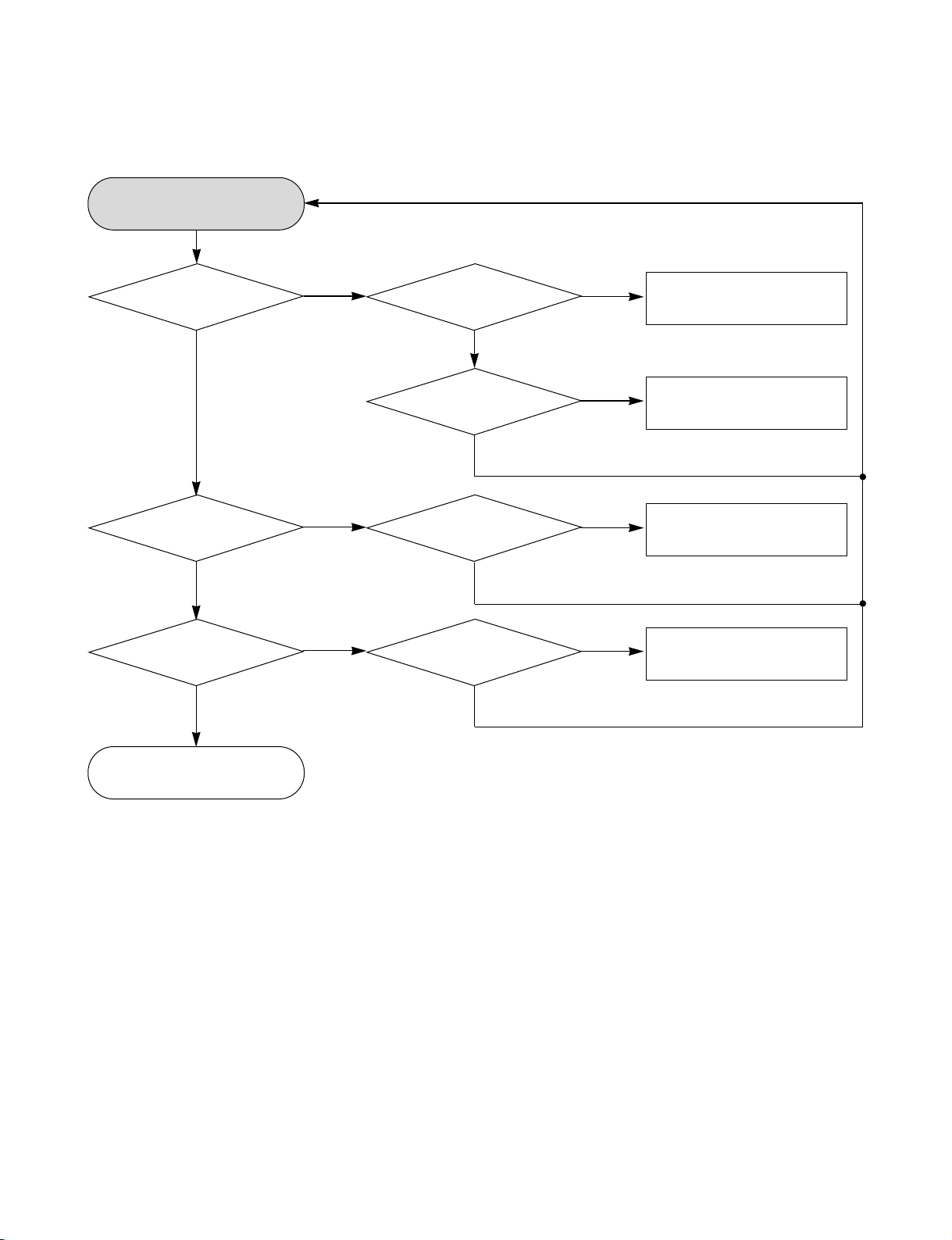
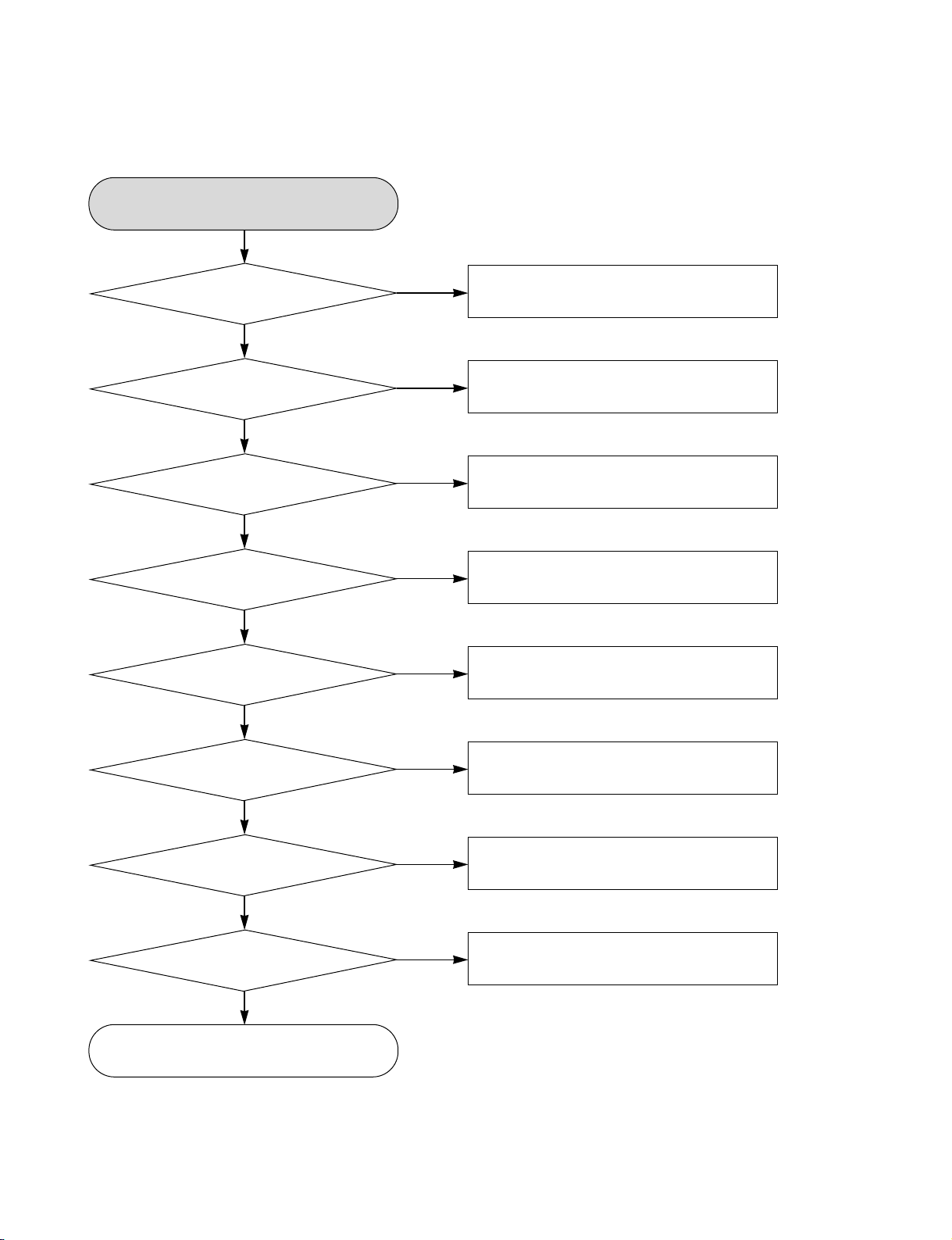
ELECTRICAL TROUBLESHOOTING GUIDE
Reset or power check.
OK
Check the power (5V/12V) short.
Repair the SMPS Block
NO
Are the pin47
of IC601+5V, pin5 of IC601+12V
respectively after the power cable
connecting?
Check the IC703 (3.3V & 1.5V regulator
& reset IC)
Check the IC301
NO
Does the pin88
(Reset) of IC301 change 0V to 3.3V
at the power supply initial input
mode?
Check the IC706
NO
Is the TP761 5V?
Check it after connecting the power cable only on
interface cable for NO Reset or Power ON.
YES
YES
Check the X301 (33.86MHz)
Check the IC301
NO
Are the X301 oscillating?
YES
Check the IC705
NO
Is the pin2, 3 of IC705 2.8V?
YES
Check the IC702
NO
Is the TP049 5.7V?
YES
Check the IC701
NO
Is the pin1 of IC701 9V?
YES
Check the IC703
NO
<Power>
Is the TP734 3.3V?
Is the TP737 1.5V?
YES
Check the IC101
NO
<Reference>
2.1V (VREF1) : Check pin83 of IC101?
2.5V (VC25) : Check pin81
of IC101?
YES
YES
YES
Page 58

4-3
ELECTRICAL TROUBLESHOOTING GUIDE
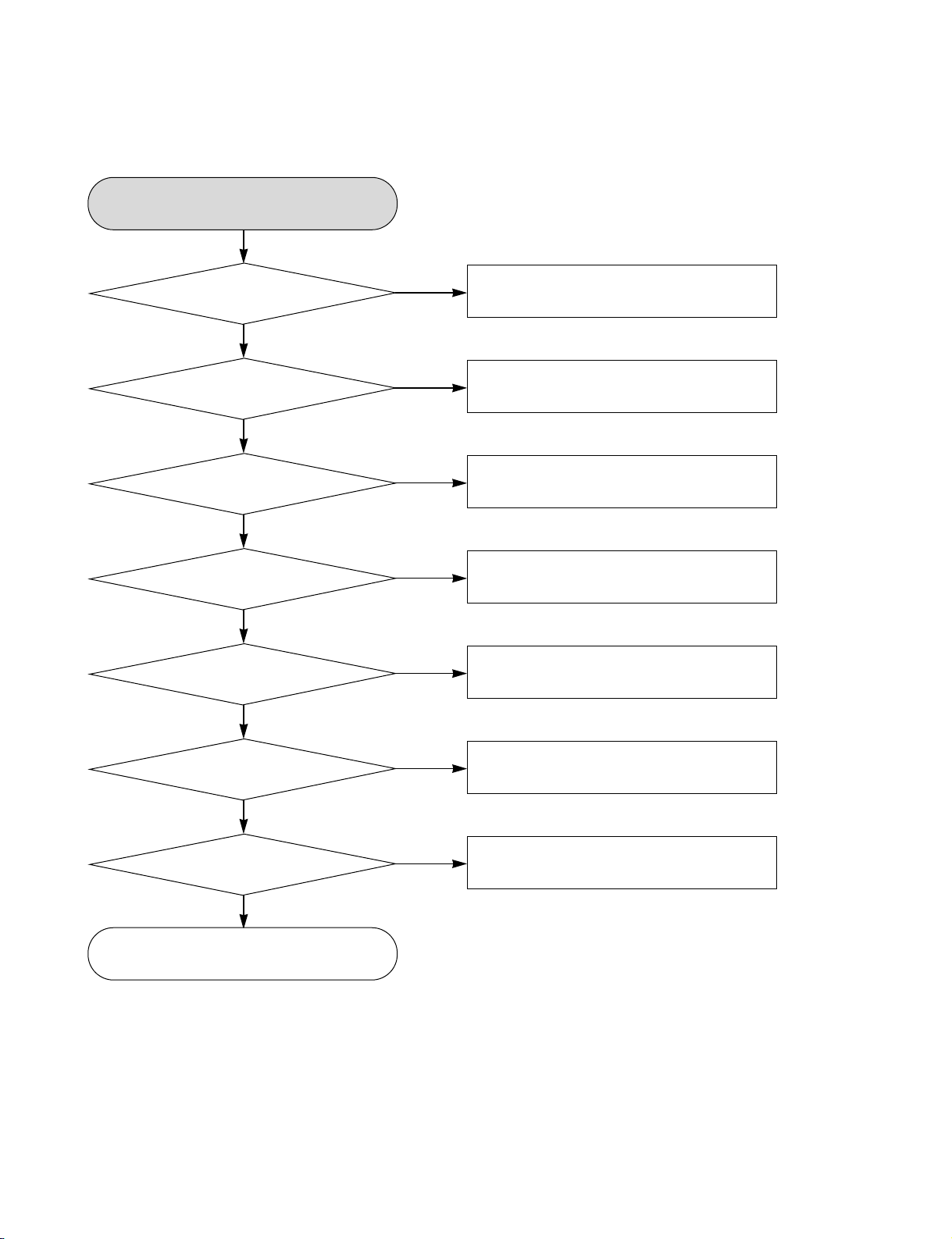
System check.
Go to “Tray operating is abnormal”
YES
YES
YES
YES
YES
YES
YES
YES
YES
NO
Does tray operate normally?
Go to “Sled operating is abnormal”
NO
Does pick-up
move to inside?
Go to “Focus actuator
operating is abnormal”
NO
Does pickup lens
move up/down?
Go to “Laser operating is abnormal”
NO
Does laser turn on?
Go to “Recognition fail case1
(DVD-ROM Disc)”
NO
Does Disc rotate
continuously and the drive
recognize the disc?
Go to “Recognition fail case2
(HD DVD-ROM)”
NO
Does Disc rotate
continuously and the drive
recognize the disc?
After eject tray, insert DVD-ROM Disc
and check rotation.
After eject the tray, insert HD DVD-ROM
disc and check rotation.
YES
YES
Go to “Recognition fail Case3
(DVD R/RW finalized disc)”
NO
Does disc rotate
continuously and the drive
recognize the disc?
After eject the tray, insert DVD R/RW
finalized disc and check rotation.
Load tray without inserting disc.
OK
Page 59

4-4
Tray operating is abnormal.
Tray open doesn’t work.
Replace the IC601.
Check the connctor (CN651)
Is there Tray
drive voltage output?
(IC601 pin38, 39)
When CN651 is
open, Is there Tray drive
signal output?
YES
YES
Is there Tray
control signal input?
(IC601 pin51)
NO
NO
NO
Check the connction of IC301 pin85
Check the communication line
(LD0 signal) between IC301 and IC601.
YES
YES
ELECTRICAL TROUBLESHOOTING GUIDE
Page 60

4-5
Sled operating is abnormal.
Check the connection
of IC301 pin7.
Check the R323, R325.
Replace the IC601.
Check the
Connection CN601
Is there
Sled drive voltage
output? (IC601 pin9,
10, 11, 12)
Is CTL1 signal “H”?
(IC601, pin27)
YES
YES
Replace the IC301.
YES
Is there
Sled drive voltage input?
(IC601 pin2, 3)
NO
NO
NO
Replace the IC301.
Is there Sled
control signal output?
(IC301 pin105, 106)
NO
YES
Replace the Sled Motor.
Is there Tray
control signal input?
(CN601 pin1, 2, 3, 4)
NO
YES
YES
ELECTRICAL TROUBLESHOOTING GUIDE
Page 61

4-6
Spindle
operating is abnormal.
Replace the IC301.
OK
Check the
connection CN602
Check the output of IC601
pin25.
Check the connector CN602.
Replace the IC301.
Is there
Spindle control DSP
output? (IC301
pin80)
YES
YES
Is there
Spindle drive voltage
output? (IC601 pin17,
18, 19)
Is there
FG signal input?
(IC301 pin78)
NO NO
NO
Replace the spindle motor.
Is there
Spindle drive voltage
output? (CN602
pin1, 2, 3)
YES
NO
YES
ELECTRICAL TROUBLESHOOTING GUIDE
Page 62

4-7
Focus servo is unstable
Replace the pick up.
Replace the IC301.
Replace the IC101.
Go to “Focus actuator
operating is abnormal”
* LIC121 pin25 is MOUT2(FEP Monitor2).
After disc recognition action, Monitor port
is off. So, please check FE signal during
disc recognition.
Is FE
signal output normal
in focusing Up/Down?
(IC101 pin4)
Check pickup
DVD read power is
1.0~1.5mW?
YES
YES
Is FDRV
signal output normal in
focusing Up/Down?
(IC301 pin108)
NO
NO
NO
YES
Focus actuator
operating is abnormal.
Check the connection of
IC301 pin7.
Replace the IC301.
Check the connection
CN101 pin49, 50.
Is there focus
search drive voltage output?
(IC601 pin45, 46)
Is
DRVMUTE2 signal “H”?
(IC601 pin27)
YES
Replace the pick-up.
Replace the IC601.
YES
Is there focus
search control signal input?
(IC601 pin50)
NO
NO
NO
• Check the connection of IC301 pin108.
• Check the communication line between
IC101 and IC301.
YES
ELECTRICAL TROUBLESHOOTING GUIDE
Page 63

4-8
Track servo is unstable
Check the pick up FFC.
Replace the pick up.
Replace the LIC201.
Replace the IC101.
Check the Drive IC
(LIC301) and P/U
referring to “Focus actuator
operating is abnormal”.
* LIC121 pin24 is MOUT1(FEP Monitor1).
After disc recognition action, Monitor port is
off. So, please check TE signal during disc
recognition.
Is TE signal
output normal in focusing
ON and tracking OFF?
(IC101 pin6)
Is PICK UP
(E, F, G, H) output
normal? (CN101 pin2,
3, 4, 5)
YES
YES
Is there TDRV
signal output in tracking ON?
(LIC201 pin66)
NO
NO
NO
YES
ELECTRICAL TROUBLESHOOTING GUIDE
Page 64

4-9
Recognition fail case 1 :
DVD-ROM fail
Go to “LD CHECK”.
YES
NO
Check pick-up read power
was 1.0~1.5mW?
Go to “Focus servo is unstable”.
YES
NO
Does focus servo
operate normally?
Check the pick-up FFC and CN101.
Replace the pick-up.
YES
NO
Check pick-up
RF signal IC101 pin77
OCRFIP was 2~2.5V?
Replace IC101.
YES
NO
Check EQOP
waveform (IC101 pin66) was
1.75~2.3V?
Go to “Tracking servo is unstable”.
YES
NO
Check after replacing IC101.
It is OK?
OK
ELECTRICAL TROUBLESHOOTING GUIDE
Page 65

4-10
Recognition fail case 2 :
HD DVD-ROM disc
Go to “LD check”.
YES
NO
Check pick up read power
was 0.5~0.8mW.
Replace the pick up.
YES
NO
Is there RF signal
at IC101 pin77?
Replace the IC101.
YES
NO
Is there
RF signal at IC101 pin77 (DCRFIP)
and pin80 (DCRFIN)?
OK
Recognition fail case 3 :
DVD R/RW finalized disc
Replace IC301.
Replace IC101.
Is there WBL
(IC101 pin27)
signal?
Is there WBL
(IC301 pin196)
signal?
YES
Check the connection
between IC101 and IC301.
YES
NO
NO
ELECTRICAL TROUBLESHOOTING GUIDE
Page 66

4-11
LD check
(Laser operating is abnormal)
Change pick up module
YES
NO
Is ALPC parameters OK?
YES
YES
NO
Is LP setting result OK?
Perform 5. Optical power setting
parameter check from “How to use Test tool”.
Perform 4. Laser power setting from
“How to use test tool?
OK
ELECTRICAL TROUBLESHOOTING GUIDE
Page 67

4-12
THE DIFFERENCES OF BLUE-RAY & DVD
1. INTRODUCTION
Page 68

4-13
2. DISC SPECIFICATION
BD-ROM DVD-ROM
Single-Layer Dual-Layer Single-Layer Dual-Layer
Media Type Read only Read only Read only Read only
User data capacity 25GB 50GB 4.7GB 8.54GB
Wavelength 405nm 405nm 650nm 650nm
Reflectivity 35~70% 12~28% 45~85% 18~30%
Track pitch 0.32um 0.32um 0.74um 0.74um
Minimum pit length 74.5nm 74.5nm 0.4um 0.4um
Modulation 17PP(d=1, k=7) EFM+ (D=2, K=10)
Error correction LDC+BIS RS production code
Channel bit-rate 66MHz 66MHz 26.16MHz 26.16MHz
Addressing 66MHz 66MHz 26.16MHz 26.16MHz
Jitter <65% <65% <8% (L0) <8%
<8.5% (L1)
<6.5% (L1, 2T/2T
not included)
1 ECC data 32 Physical sector (64KB) 16 Physical sector (32KB)
Numerical Aperture 0.85 0.6
Protection Layer 0.1mm 0.1mm(L0) 0.6mm 0.6mm
(Cover Layer) 0.075mm(L1)
Hard coating Yes No
Data transfer rate(data) 36Mbps (1x) 11.08Mbps (1x)
Data transfer rate(A/V) 54Mbps (1.5x) 10.08Mbps (<1x)
Video resolution(max) 1920x1080 (1080p) 720x480/720x576 (480i/576i)
Video bit rate(max) 40.0Mbps 9.8Mbps
Video codecs MPEG-2 MPEG-2
MPEG-4AVC -
SMPTE VC-1 -
Audio codecs Linear PCM Linear PCM
Dolby Digital Dolby Digital
Dolby Digital Plus DTS Digital Surround
Dolby TrueHD -
DTS Digital Surround -
DTS-HD -
Interactivity BD-J DVD-Vide
Page 69

4-14
3. FORMAT OF THE INFORMATION ZONE
Page 70

4-15
BCA : Used to add information to the disc after completion of the manufacturing process
Protection zone1 : Protection area against overwriting of the PIC by the BCA
Protection zone2 : Changeover area for the track pitch(0.35um 0.32um)
PIC Zone : General information about the disc
INFO/reserved : Information zone/reserved
Data Zone : User Data Area
Page 71

4-16
HOW TO USE TEST TOOL
1. ALPC MEASUREMENT SYSTEM COMPOSITION
To measure and adjust the optical power of DVD, BD and HD-DVD, you must basically have the following
measuring device.
(1) Optical power meter & sensor (ADVANTEST, Q8230/Q82313 (RED), Q82312 (Blue) or equivalent product)
(2) Personal computer
(3) Program for adjustment (LP setting tool)
(4) USB-SATA interface (This is needed when using a notebook without SATA interface or when using USB
port on the PC.)
Optical power meter Personal computer
Loader ass'y USB-SATA interface
LP setting tool
Page 72

4-17
2. ALPC PROGRAM COMPOSITION
ALPC program is composed of two files.
LPSettingTool.exe
PCAL.CFG
These two files must be located in the same directory.
PSettingTool.exe is the execution file of the program and PCAL.CFG is the configuration file related to LP
Setting.
Decision of connection method
When you initially execute the LPSettingTool.exe file, you
will see a menu to select how to communicate with the
target system as shown in the left figure.
Use serial communication
Select Test LD
Display LP
setting results
Display execution
results OK/NG
Initialize button of
displayed results
Check execute results
Display HFM frequency
setting results
Laser power setting
start button
Disconnect communication
Use AAPI communication
Page 73

4-18
3. EXECUTE ALPC PROGRAM
(1) Execute the LPSettingTool.exe file.
(2) Click on the ATAPI icon to communicate with
the target system through ATAPI.
(3) Click on the Trigger button.
The results are displayed.
Page 74

4-19
4. LASER POWER SETTING
When replacing the Travers assembly including the pick-up or replacing the loader PCB, you must execute
the optical power setting to match the pick-up with the loader PCB.
When you click on the button in the condition shown above left, the optical power setting will be
executed in the order of DVD, BD and HD-DVD LD as shown on the right side to display whether OK/NG with
the results.
Trigger
Page 75

4-20
5. LASER POWER SETTING PARAMETER CHECK
Current defects can be realized but when the optical power setting result is OK, you need to check whether
the existing setting values are set correctly. In this case, when you press the button, the ALPC
Parameter Information window will be displayed to display the optical power setting value recorded in current
EEPROM. After taking note of this in a separate memo execute the optical power setting and press the
button again to display new optical power setting value. Compare the two parameters and if there is a big
gap, it means that either the initial optical power setting is done improperly or the optical output of the pick-
up has changed. If the pick-up is judged to be normal, you can reset the optical power to resolve the issue
without having to replace the pick-up. In order to delete the existing ALPC parameter from the ALPC
Parameter Info window, press the button on the bottom of the ALPC Parameter Info window.
Clear
Page 76

4-21
The PACL.CFG file in the directory where the execution file is located shows the valid range of the ALPC
parameter by LD.
Check whether each parameter value displayed in the ALPC Parameter Information window is regressing
within the low/high limit set in the PACL.CFG file, and if not the optical power setting is not done properly.
PACL.CFG file content
Page 77

4-22
6. HOW TO MEASURE LASER POWER
The optical power measurement is measuring the optical power actually emitted from the object lens with the
LD turned on. Therefore to measure the optical power, the LD must be turned on and the darker the better. If
needed, cover the top of the sensor with a dark paper or hand for measurement. Generally since the
florescent light is about 50 _W and sunlight about 100 _W, ignoring these lights can results in wrong setting
of the optical power. Therefore you must be careful.
Procedure for measuring the optical power
1. Set the _ (wave length) of the optical power meter to the DVD. (Generally 650nm)
2. Turn on the DVD LD.
3. Put the sensor within 3m from the object lens of the pick-up and locate the lens in a right angle.
Adjust the location so that the center of the object lens and the _ sign on the sensor are aligned.
4. Read the value on the monitor. (Read the maximum value while slightly moving the location.)
(Check the unit. The unit must be mW. When the LD is dead, you can mistakenly read the unit of _W or nW.)
5. Multiply 100 to the value on the monitor and round off to the nearest integer to write the integer part.)
6. Set the _ (wave length) of the optical power meter to the BD.
(Generally 405nm)
7. Turn on the BD LD.
8. Execute from 3 to 5 from the above.
9. Set the _ (wave length) of the optical power meter to the HD.
(Generally 405nm)
10.Turn on the HD-DVD LD.
11. Execute from 3 to 5 from the above.
Page 78

4-23
INTERNAL BLOCK DIAGRAM OF IC
1. R2S30220SP
1-1. BLOCK DIAGRAM
1-2. PIN FUNCTION
Termianl Symbol Termianl function Termianl Symbol Termianl function
1 SPIN Spindle control voltage input 27 EN1 Input terminal for enable 1
2 SL1IN Slide control voltage input 1 28 EN2 *1 Input terminal for enable 2
3 SL2IN Slide control voltage input 2 29 STES
Input terminal for Excitation off select ST
4 SPLIM
Input terminal for spindle current limit
30 ACTRST*2 Pickup protect Reset
5 VM2 Motor Power Supply 2 (for Slide12) 31 VM4 Power Supply£¥(for Stepper)
6 ST1IN Steppe control voltage input 1 32 ST1+ Steppe non-inverted output 1
7 ST2IN Steppe control voltage input £≤ 33 ST1- Steppe inverted output 1
8 LCIN Liquid crystal control voltage input 34 ST2+ Steppe non-inverted output 2
9 SL2+ Slide non-inverted output 2 35 ST2 Steppe inverted output 2
10 SL2 Slide inverted output 2 36 VM3 Power Supply3(for Loading)
11 GND GND 37 GND GND
12 SL1+ Slide non-inverted output 38 LO+ Loading non-inverted output
13 SL1- Slide inverted output 1 39 LO- Loading inverted output
14 LC+ Liquid crystal non-inverted output 40 TL+ Tilt non-inverted output
15 LC- Liquid crystal inverted output 41 TL- Tilt inverted output
16 GND GND 42 GND GND
17 U Motor drive output U 43 TO- Tracking inverted output
18 V Motor drive output V 44 TO+ Tracking non-inverted output
19 W Motor drive output W 45 FO+ Focus non-inverted output
20 COMMON Motor common 46 FO- Focus inverted output
21 VM5
Motor Power Supply5(for Liquid crystal)
47 5VCC 5V Power Supply (for FS,TS,TL)
22 STLIM
Input terminal for stepper current limit
48 TLIN Tilt control voltage input
23 SLLIM Input terminal for slide current limit 49 TOIN Tracking control voltage input
24 ACTFLG Pickup protect flag output 50 FOIN Focus control voltage input
25 FG Frequency generator output 51 LOIN Loading control input
26 VM1 Motor Power Supply 1(for Spindle) 52 REF Reference voltage input
Page 79

4-24
2. R8J32700FPV
2-1. PIN LAYOUT
Page 80

4-25
2-2. BLOCK DIAGRAM
Page 81

4-26
2-3. PIN FUNCTION
Page 82

4-27
3. R2S35003
3-1. PIN ASSIGNMENT
Page 83

4-28
3-2. BLOCK DIAGRAM
Page 84

4-29
3-3. PIN FUNCTIONS
Page 85

4-30
Page 86

4-31
WAVEFORMS
1. POWER & RESET SIGNAL
12V (CN803, PIN20, 21, 22)
5V(CN803, PIN14, 15, 16)
HRST (IC301, PIN209)
MRSTB (IC301, PIN88)
2. MAIN CLOCK1 FOR IC301 (33.859MHz)
X301 (IC301, PIN3)
Page 87

4-32
3. MAIN CLOCK2 FOR IC707 (25.035MHz)
X302 (IC707, PIN23)
Open sw (CN651 PIN3)
Close sw (CN651 PIN5)
Tray + (CN651 PIN2)
Tray - (CN651 PIN4)
4. TRAY OPEN/CLOSE SIGNAL
A
Open sw
Close sw
Tray +
Tray -
OPEN OPERATION
CLOSE OPERATION
B C D
Page 88

4-33
Open sw (CN651 PIN3) LDD (IC601 PIN51)
Tray + (CN651 PIN2) Tray - (CN651 PIN4)
5. TRAY OPEN/CLOSE SIGNAL A
6. TRAY OPEN/CLOSE SIGNAL B
Open sw (CN651 PIN3)
Open sw
LDO
Tray +
Tray -
ZOOM
A: STANDBY STATUS
Open sw (CN651 PIN3) LDD (IC601 PIN51)
Tray + (CN651 PIN2) Tray - (CN651 PIN4)
Open sw (CN651 PIN3)
Open sw
LDO
Tray +
Tray -
ZOOM
B : OPEN INITIAL STATUS
Page 89

4-34
Open sw (CN651 PIN3) LDD (IC601 PIN51)
Tray + (CN651 PIN2) Tray - (CN651 PIN4)
7. TRAY OPEN/CLOSE SIGNAL C
8. TRAY OPEN/CLOSE SIGNAL D
Open sw (CN651 PIN3)
Close sw
LDO
Tray +
Tray -
ZOOM
C : OPEN FINISHED STATUS
Open sw (CN651 PIN3) LDD (IC601 PIN51)
Tray + (CN651 PIN2) Tray - (CN651 PIN4)
Open sw (CN651 PIN3)
Close sw
LDO
Tray +
Tray -
ZOOM
D : CLOSE STATUS
Page 90

4-35
9. SLED MOVE SIGNAL
A+ (CN601 PIN4)
A- (CN601 PIN3)
B+ (CN601 PIN2)
B- (CN601 PIN1)
10. ZOOM OF SLED MOVE SIGNAL
A+ (CN601 PIN4)
A- (CN601 PIN3)
B+ (CN601 PIN2)
B- (CN601 PIN1)
Page 91

4-36
11. SPINDLE WAVEFORM
U (CN602 PIN3)
V (CN602 PIN2)
W (CN602 PIN1)
FG (IC601 PIN25)
12. ZOOM OF SPINDLE WAVEFORM
U (CN602 PIN3)
V (CN602 PIN2)
W (CN602 PIN1)
FG (IC601 PIN25)
Page 92

4-37
13. DISC TYPE JUDGEMENT WAVEFORM (DVD SERIES)
FE (IC101 PIN4)
FOD (IC601 PIN50)
TYPE JUGDEMENT
FOCUS ON
14. DISC TYPE JUDGEMENT WAVEFORM (DVD_SINGLE)
FE (IC101 PIN4)
FOD (IC601 PIN50)
Page 93

4-38
15. DISC TYPE JUDGEMENT WAVEFORM (DVD_DUAL)
FE (IC101 PIN4)
FOD (IC601 PIN50)
16. DISC TYPE JUDGEMENT WAVEFORM (BD SERIES)
FE (IC101 PIN4)
FOD (IC601 PIN50)
FOCUS ON
TYPE JUGDEMENT
Page 94

4-39
17. DISC TYPE JUDGEMENT WAVEFORM (BD_SINGLE)
FE (IC101 PIN4)
FOD (IC601 PIN50)
18. DISC TYPE JUDGEMENT WAVEFORM (BD_DUAL)
FE (IC101 PIN4)
FOD (IC601 PIN50)
Page 95

4-40
19. DISC TYPE JUDGEMENT WAVEFORM (HD SERIES)
FE (IC101 PIN4)
FOD (IC601 PIN50)
TYPE JUGDEMENT
FOCUS ON
20. DISC TYPE JUDGEMENT WAVEFORM (HD_SINGLE)
FE (IC101 PIN4)
FOD (IC601 PIN50)
Page 96

4-41
21. DISC TYPE JUDGEMENT WAVEFORM (HD_DUAL)
FE (IC101 PIN4)
FOD (IC601 PIN50)
22. FOCUS ON SIGNAL (DVD)
FE (IC101 PIN4)
FOD (IC601 PIN50)
TE (IC101 PIN5)
TRD (IC601 PIN49)
Page 97

4-42
23. FOCUS ON SIGNAL (BD)
FE (IC101 PIN4)
FOD (IC601 PIN50)
TE (IC101 PIN5)
TRD (IC601 PIN49)
24. FOCUS ON SIGNAL (HD)
FE (IC101 PIN4)
FOD (IC601 PIN50)
TE (IC101 PIN5)
TRD (IC601 PIN49)
Page 98

4-43
25. TRACK OFF SIGNAL (DVD)
TE (IC101 PIN5)
TZC (IC101 PIN43)
MIRR (IC101 PIN49)
26. TRACK OFF SIGNAL (BD)
TE (IC101 PIN5)
TZC (IC101 PIN43)
MIRR (IC101 PIN49)
Page 99

4-444-44
27. TRAKC OFF SIGNAL (HD)
TE (IC101 PIN5)
TZC (IC101 PIN43)
MIRR (IC101 PIN49)
28. TILT DRIVER SIGNAL
TLD (IC601 PIN48)
TILT+ (IC601 PIN40)
TILT- (IC601 PIN41)
Page 100

4-454-45
29. WOBBLE (DVD - R/RW)
AWOBSIG (IC101 PIN27)
LPPOUT (IC101 PIN51)
30. WOBBLE (DVD + R/RW)
WOBSIG (IC101 PIN48)
AWOBSIG (IC101 PIN27)
 Loading...