

Page 1

R
LCD TV
SERVICE MANUAL
CAUTION
BEFORE SERVICING THE CHASSIS,
READ THE SAFETY PRECAUTIONS IN THIS MANUAL.
CHASSIS : LD61C
MODEL : 42LC2D 42LC2D-FC
North/Latin America http://aic.lgservice.com
Europe/Africa http://eic.lgservice.com
Asia/Oceania http://biz.lgservice.com
Page 2

LGE Internal Use OnlyCopyright © 2006 LG Electronics. Inc. All right reserved.
Only for training and service purposes
- 2 -
CONTENTS
CONTENTS .............................................................................................. 2
PRODUCT SAFETY ..................................................................................3
SPECIFICATION ........................................................................................6
ADJUSTMENT INSTRUCTION ...............................................................10
TROUBLE SHOOTING ............................................................................14
BLOCK DIAGRAM...................................................................................27
EXPLODED VIEW .................................................................................. 29
SVC. SHEET ...............................................................................................
Page 3
LGE Internal Use OnlyCopyright © 2006 LG Electronics. Inc. All right reserved.
Only for training and service purposes
- 3 -
SAFETY PRECAUTIONS
Many electrical and mechanical parts in this chassis have special safety-related characteristics. These parts are identified by in the
Schematic Diagram and Exploded View.
It is essential that these special safety parts should be replaced with the same components as recommended in this manual to prevent
Shock, Fire, or other Hazards.
Do not modify the original design without permission of manufacturer.
General Guidance
An isolation Transformer should always be used during the
servicing of a receiver whose chassis is not isolated from the AC
power line. Use a transformer of adequate power rating as this
protects the technician from accidents resulting in personal injury
from electrical shocks.
It will also protect the receiver and it's components from being
damaged by accidental shorts of the circuitry that may be
inadvertently introduced during the service operation.
If any fuse (or Fusible Resistor) in this TV receiver is blown,
replace it with the specified.
When replacing a high wattage resistor (Oxide Metal Film Resistor,
over 1W), keep the resistor 10mm away from PCB.
Keep wires away from high voltage or high temperature parts.
Before returning the receiver to the customer,
always perform an AC leakage current check on the exposed
metallic parts of the cabinet, such as antennas, terminals, etc., to
be sure the set is safe to operate without damage of electrical
shock.
Leakage Current Cold Check(Antenna Cold Check)
With the instrument AC plug removed from AC source, connect an
electrical jumper across the two AC plug prongs. Place the AC
switch in the on position, connect one lead of ohm-meter to the AC
plug prongs tied together and touch other ohm-meter lead in turn to
each exposed metallic parts such as antenna terminals, phone
jacks, etc.
If the exposed metallic part has a return path to the chassis, the
measured resistance should be between 1MΩ and 5.2MΩ.
When the exposed metal has no return path to the chassis the
reading must be infinite.
An other abnormality exists that must be corrected before the
receiver is returned to the customer.
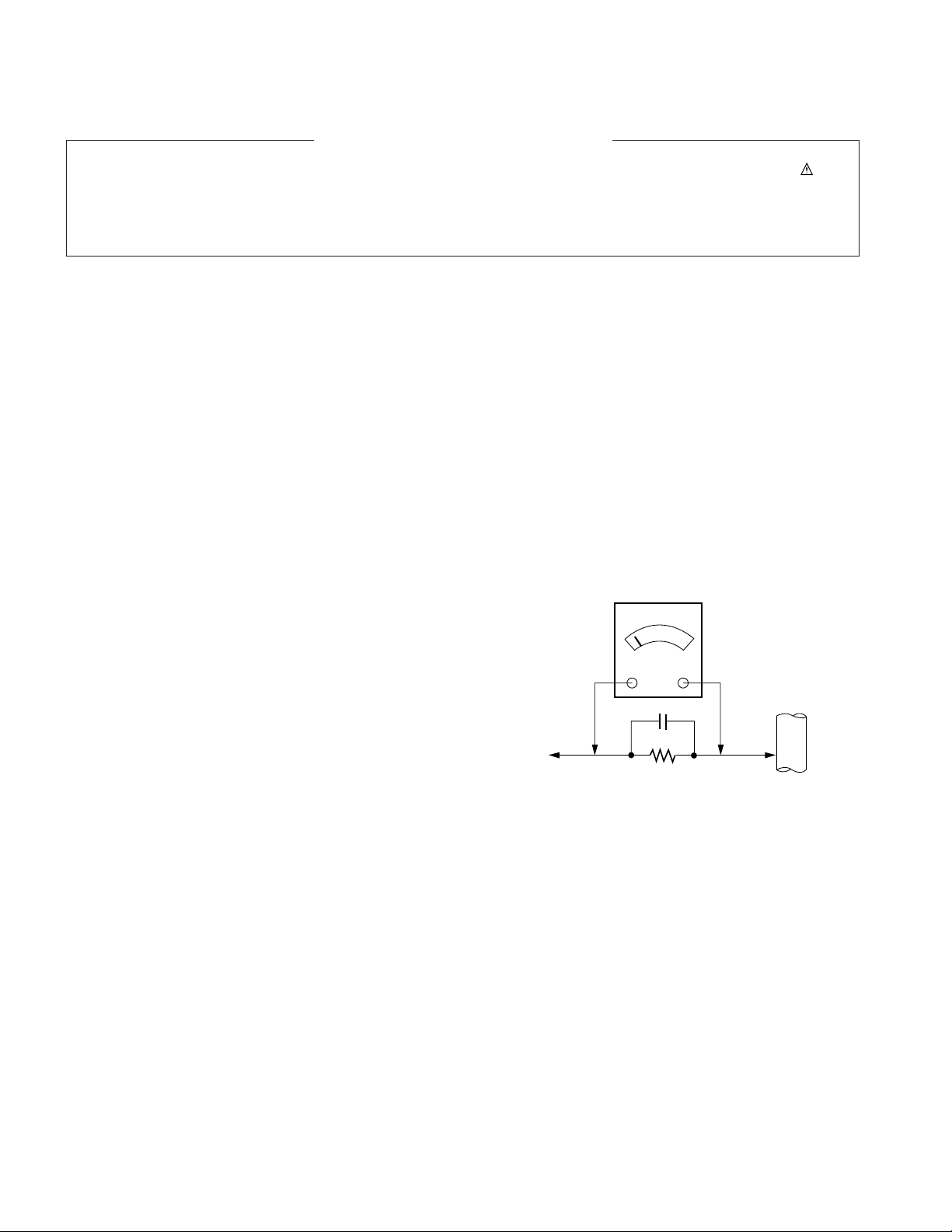
Leakage Current Hot Check (See below Figure)
Plug the AC cord directly into the AC outlet.
Do not use a line Isolation Transformer during this check.
Connect 1.5K/10watt resistor in parallel with a 0.15uF capacitor
between a known good earth ground (Water Pipe, Conduit, etc.)
and the exposed metallic parts.
Measure the AC voltage across the resistor using AC voltmeter
with 1000 ohms/volt or more sensitivity.
Reverse plug the AC cord into the AC outlet and repeat AC voltage
measurements for each exposed metallic part. Any voltage
measured must not exceed 0.75 volt RMS which is corresponds to
0.5mA.
In case any measurement is out of the limits specified, there is
possibility of shock hazard and the set must be checked and
repaired before it is returned to the customer.
Leakage Current Hot Check circuit
1.5 Kohm/10W
To Instrument's
exposed
METALLIC PARTS
Good Earth Ground
such as WATER PIPE,
CONDUIT etc.
AC Volt-meter
IMPORTANT SAFETY NOTICE
0.15uF
Page 4

LGE Internal Use OnlyCopyright © 2006 LG Electronics. Inc. All right reserved.
Only for training and service purposes
- 4 -
CAUTION: Before servicing receivers covered by this service
manual and its supplements and addenda, read and follow the
SAFETY PRECAUTIONS on page 3 of this publication.
NOTE: If unforeseen circumstances create conflict between the
following servicing precautions and any of the safety precautions on
page 3 of this publication, always follow the safety precautions.
Remember: Safety First.
General Servicing Precautions
1. Always unplug the receiver AC power cord from the AC power
source before;
a. Removing or reinstalling any component, circuit board
module or any other receiver assembly.
b. Disconnecting or reconnecting any receiver electrical plug or
other electrical connection.
c. Connecting a test substitute in parallel with an electrolytic
capacitor in the receiver.
CAUTION: A wrong part substitution or incorrect polarity
installation of electrolytic capacitors may result in an
explosion hazard.
2. Test high voltage only by measuring it with an appropriate high
voltage meter or other voltage measuring device (DVM,
FETVOM, etc) equipped with a suitable high voltage probe.
Do not test high voltage by "drawing an arc".
3. Do not spray chemicals on or near this receiver or any of its
assemblies.
4. Unless specified otherwise in this service manual, clean
electrical contacts only by applying the following mixture to the
contacts with a pipe cleaner, cotton-tipped stick or comparable
non-abrasive applicator; 10% (by volume) Acetone and 90% (by
volume) isopropyl alcohol (90%-99% strength)
CAUTION: This is a flammable mixture.
Unless specified otherwise in this service manual, lubrication of
contacts in not required.
5. Do not defeat any plug/socket B+ voltage interlocks with which
receivers covered by this service manual might be equipped.
6. Do not apply AC power to this instrument and/or any of its
electrical assemblies unless all solid-state device heat sinks are
correctly installed.
7. Always connect the test receiver ground lead to the receiver
chassis ground before connecting the test receiver positive
lead.
Always remove the test receiver ground lead last.
8. Use with this receiver only the test fixtures specified in this
service manual.
CAUTION: Do not connect the test fixture ground strap to any
heat sink in this receiver.
Electrostatically Sensitive (ES) Devices
Some semiconductor (solid-state) devices can be damaged easily
by static electricity. Such components commonly are called
Electrostatically Sensitive (ES) Devices. Examples of typical ES
devices are integrated circuits and some field-effect transistors and
semiconductor "chip" components. The following techniques
should be used to help reduce the incidence of component
damage caused by static by static electricity.
1. Immediately before handling any semiconductor component or
semiconductor-equipped assembly, drain off any electrostatic
charge on your body by touching a known earth ground.
Alternatively, obtain and wear a commercially available
discharging wrist strap device, which should be removed to
prevent potential shock reasons prior to applying power to the
unit under test.
2. After removing an electrical assembly equipped with ES
devices, place the assembly on a conductive surface such as
aluminum foil, to prevent electrostatic charge buildup or
exposure of the assembly.
3. Use only a grounded-tip soldering iron to solder or unsolder ES
devices.
4. Use only an anti-static type solder removal device. Some solder
removal devices not classified as "anti-static" can generate
electrical charges sufficient to damage ES devices.
5. Do not use freon-propelled chemicals. These can generate
electrical charges sufficient to damage ES devices.
6. Do not remove a replacement ES device from its protective
package until immediately before you are ready to install it.
(Most replacement ES devices are packaged with leads
electrically shorted together by conductive foam, aluminum foil
or comparable conductive material).
7. Immediately before removing the protective material from the
leads of a replacement ES device, touch the protective material
to the chassis or circuit assembly into which the device will be
installed.
CAUTION: Be sure no power is applied to the chassis or circuit,
and observe all other safety precautions.
8. Minimize bodily motions when handling unpackaged
replacement ES devices. (Otherwise harmless motion such as
the brushing together of your clothes fabric or the lifting of your
foot from a carpeted floor can generate static electricity
sufficient to damage an ES device.)
General Soldering Guidelines
1. Use a grounded-tip, low-wattage soldering iron and appropriate
tip size and shape that will maintain tip temperature within the
range or 500ºF to 600ºF.
2. Use an appropriate gauge of RMA resin-core solder composed
of 60 parts tin/40 parts lead.
3. Keep the soldering iron tip clean and well tinned.
4. Thoroughly clean the surfaces to be soldered. Use a mall wirebristle (0.5 inch, or 1.25cm) brush with a metal handle.
Do not use freon-propelled spray-on cleaners.
5. Use the following unsoldering technique
a. Allow the soldering iron tip to reach normal temperature.
(500ºF to 600ºF)
b. Heat the component lead until the solder melts.
c. Quickly draw the melted solder with an anti-static, suction-
type solder removal device or with solder braid.
CAUTION: Work quickly to avoid overheating the circuit
board printed foil.
6. Use the following soldering technique.
a. Allow the soldering iron tip to reach a normal temperature
(500ºF to 600ºF)
b. First, hold the soldering iron tip and solder the strand against
the component lead until the solder melts.
c. Quickly move the soldering iron tip to the junction of the
component lead and the printed circuit foil, and hold it there
only until the solder flows onto and around both the
component lead and the foil.
CAUTION: Work quickly to avoid overheating the circuit
board printed foil.
d. Closely inspect the solder area and remove any excess or
splashed solder with a small wire-bristle brush.
SERVICING PRECAUTIONS
Page 5

LGE Internal Use OnlyCopyright © 2006 LG Electronics. Inc. All right reserved.
Only for training and service purposes
- 5 -
IC Remove/Replacement
Some chassis circuit boards have slotted holes (oblong) through
which the IC leads are inserted and then bent flat against the
circuit foil. When holes are the slotted type, the following technique
should be used to remove and replace the IC. When working with
boards using the familiar round hole, use the standard technique
as outlined in paragraphs 5 and 6 above.
Removal
1. Desolder and straighten each IC lead in one operation by gently
prying up on the lead with the soldering iron tip as the solder
melts.
2. Draw away the melted solder with an anti-static suction-type
solder removal device (or with solder braid) before removing the
IC.
Replacement
1. Carefully insert the replacement IC in the circuit board.
2. Carefully bend each IC lead against the circuit foil pad and
solder it.
3. Clean the soldered areas with a small wire-bristle brush.
(It is not necessary to reapply acrylic coating to the areas).
"Small-Signal" Discrete Transistor
Removal/Replacement
1. Remove the defective transistor by clipping its leads as close as
possible to the component body.
2. Bend into a "U" shape the end of each of three leads remaining
on the circuit board.
3. Bend into a "U" shape the replacement transistor leads.
4. Connect the replacement transistor leads to the corresponding
leads extending from the circuit board and crimp the "U" with
long nose pliers to insure metal to metal contact then solder
each connection.
Power Output, Transistor Device
Removal/Replacement
1. Heat and remove all solder from around the transistor leads.
2. Remove the heat sink mounting screw (if so equipped).
3. Carefully remove the transistor from the heat sink of the circuit
board.
4. Insert new transistor in the circuit board.
5. Solder each transistor lead, and clip off excess lead.
6. Replace heat sink.
Diode Removal/Replacement
1. Remove defective diode by clipping its leads as close as
possible to diode body.
2. Bend the two remaining leads perpendicular y to the circuit
board.
3. Observing diode polarity, wrap each lead of the new diode
around the corresponding lead on the circuit board.
4. Securely crimp each connection and solder it.
5. Inspect (on the circuit board copper side) the solder joints of
the two "original" leads. If they are not shiny, reheat them and if
necessary, apply additional solder.
Fuse and Conventional Resistor
Removal/Replacement
1. Clip each fuse or resistor lead at top of the circuit board hollow
stake.
2. Securely crimp the leads of replacement component around
notch at stake top.
3. Solder the connections.
CAUTION: Maintain original spacing between the replaced
component and adjacent components and the circuit board to
prevent excessive component temperatures.
Circuit Board Foil Repair
Excessive heat applied to the copper foil of any printed circuit
board will weaken the adhesive that bonds the foil to the circuit
board causing the foil to separate from or "lift-off" the board. The
following guidelines and procedures should be followed whenever
this condition is encountered.
At IC Connections
To repair a defective copper pattern at IC connections use the
following procedure to install a jumper wire on the copper pattern
side of the circuit board. (Use this technique only on IC
connections).
1. Carefully remove the damaged copper pattern with a sharp
knife. (Remove only as much copper as absolutely necessary).
2. carefully scratch away the solder resist and acrylic coating (if
used) from the end of the remaining copper pattern.
3. Bend a small "U" in one end of a small gauge jumper wire and
carefully crimp it around the IC pin. Solder the IC connection.
4. Route the jumper wire along the path of the out-away copper
pattern and let it overlap the previously scraped end of the good
copper pattern. Solder the overlapped area and clip off any
excess jumper wire.
At Other Connections
Use the following technique to repair the defective copper pattern
at connections other than IC Pins. This technique involves the
installation of a jumper wire on the component side of the circuit
board.
1. Remove the defective copper pattern with a sharp knife.
Remove at least 1/4 inch of copper, to ensure that a hazardous
condition will not exist if the jumper wire opens.
2. Trace along the copper pattern from both sides of the pattern
break and locate the nearest component that is directly
connected to the affected copper pattern.
3. Connect insulated 20-gauge jumper wire from the lead of the
nearest component on one side of the pattern break to the lead
of the nearest component on the other side.
Carefully crimp and solder the connections.
CAUTION: Be sure the insulated jumper wire is dressed so the
it does not touch components or sharp edges.
Page 6
LGE Internal Use OnlyCopyright © 2006 LG Electronics. Inc. All right reserved.
Only for training and service purposes
- 6 -
SPECIFICATION
NOTE : Specifications and others are subject to change without notice for improvement
.
1. General Specification(TV)
No Item Specification Remark
1. Video input applicable system PAL-D/K, B/G, I, NTSC-M, SECAM
NTSC 4.43
2. Receivable Broadcasting System 1) PAL/SECAM BG EU/Non-EU
2) PAL/SECAM DK (PAL Market)
3) PAL I/I
4) SECAM L/L'
5) PAL-N/M Central and South America Market
6) NTSC M
3. RF Input Channel VHF : E2 ~ E12 PAL
UHF : E21 ~ E69
CATV : S1 ~ S20
HYPER : S21~ S47
L/L' : B, C, D FRANCE
VHF : 2~13 NTSC
UHF : 14~69
CATV : 1~125
VHF Low : 1 ~ M10 JAPAN
VHF High : 4~S22
UHF : S23~62
4. Input Voltage AC 100-240V~/ 50Hz, 60Hz
5. Market France
6. Picture Size 1067.308(diagonal) 42 inch
7. Tuning System FVS 100 program PAL, 200 PR.(Option)
FS NTSC
8. Operating Environment 1) Temp : 0 ~ 40 deg
2) Humidity : 10~90 %
9. Storage Environment 3) Temp : -20 ~ 50 deg
4) Humidity : 10~90 %
10. Display LCD Module LPL
Page 7
LGE Internal Use OnlyCopyright © 2006 LG Electronics. Inc. All right reserved.
Only for training and service purposes
- 7 -
2. General Specification
No Item Specification Remark
1 Panel 42" TFT WXGA LCD
2 Frequency range H : 31 ~ 61Khz PC Input
V : 56 ~ 75Hz
3 Control Function 1) Contrast/Brightness
2) H-Position / V-Position
3) Tracking : Clock / Phase
4) Auto Configure
5) Reset
4 Component Jack 1 : Y Middle east / NTSC Area
3 : Pb
5 : Pr
5 H/V-Sync Video Power consumption LED
Power ON - -
≤ 240W(42")
Green
Stand by
≤ 3.0W
Red
Power off - - - *
6 LCD Module Type Size 42” 1006 x 610 x 56(mm) (H) x (V) x (D)
Pixel Pitch 42” 0.227 x 0.681 x RGB µm
Pixel Format 1366 horiz. By 768 vert.
Pixels RGB strip arrangement
Coating Hard coating(3H), Anti-glare
reatment of the front polarizer,
Back Light 42" 20CCFL
No Item Specification Min. Typ. Max. Remark
1 Viewing Angle <CR>10> R/L, U/D 178, 178
2 Luminance Luminance(cd/m
2
) 400 500 32/37/42
Variation 1.3 MAX/MIN
3 Contrast Ratio CR 400 550 All White/All Black
CR
D(With AL) 800 1100 All White/All Black
4 CIE Color Coordinates White Wx Typ 0.281 Typ LPL(42")
Wy -0.03 0.293 +0.03
Red Xr 0.639
Yr 0.340
Green Xg 0.284
Yg 0.604
Blue Xb 0.145
Yb 0.064
3. Optical Feature(LCD Module)
Page 8
LGE Internal Use OnlyCopyright © 2006 LG Electronics. Inc. All right reserved.
Only for training and service purposes
No Resolution H-freq(kHz) V-freq.(Hz) Pixel clock(MHz) Proposed
1 720x576 31.25 50.00 SDTV 576p 50Hz
2 720x480 31.47 59.94 SDTV 480p 60Hz
3 1280x720 45.00 50.00 HDTV 720p 50Hz HDCP
4 1280x720 44.96 59.94 HDTV 720p 60Hz HDCP
5 1920x1080 28.13 50.00 HDTV 1080i 50Hz HDCP
6 1920x1080 33.72 59.94 HDTV 1080i 60Hz HDCP
- 8 -
4. Component Video Input (Y, P
B, PR)
No.
Specification
Remark
Resolution H-freq(kHz) V-freq(Hz)
1. 720x480 15.73 60 SDTV, DVD 480i
2. 720x480 15.63 59.94 SDTV, DVD 480i
3. 720x480 31.47 59.94 EDTV 480p
4. 720x576 15.625 50.00 SDTV, DVD 625 Line
5. 720x576 31.25 50.00 HDTV 576p
6. 1280x720 45.00 60.00 HDTV 720p
7. 1280x720 44.96 59.94 HDTV 720p
8. 1920x1080 31.25 50.00 HDTV 1080i
9. 1920x1080 33.75 60.00 HDTV 1080i
10. 1920x1080 33.72 59.94 HDTV 1080i
5. RGB PC INPUT Mode Table
No Resolution H-freq(kHz) V-freq.(Hz) Pixel clock(MHz) Proposed
Analog RGB, Digital RGB
1 720x400 31.468 70.8 28.321
2 640x480 31.469 59.94 25.17 VESA
37.684 75.00 31.5 VESA
3 800x600 37.879 60.31 40.00 VESA
46.875 75 49.5 VESA
4 832x624 49.725 74.55 57.283
5 1024x768 48.363 60.00 65.00 VESA(XGA)
56.47 70.00 75.00 VESA(XGA)
60.123 75.029 78.75 VESA(XGA)
6 1280x768 47.776 59.870 79.50 VESA(WXGA)
7 1360x768 47.720 59.799 84.75 VESA(WXGA)
8 1366x768 47.720 59.799 84.75 Supported
6. RGB DTV INPUT Mode Table
Page 9
LGE Internal Use OnlyCopyright © 2006 LG Electronics. Inc. All right reserved.
Only for training and service purposes
- 9 -
7. HDMI INPUT Mode Table
8. HDMI DTV Mode Table
No Resolution H-freq(kHz) V-freq.(Hz) Pixel clock(MHz) Proposed
Analog RGB, Digital RGB
1 720x400 31.468 70.8 28.321
2 640x480 31.469 59.94 25.17 VESA
37.684 75.00 31.5 VESA
3 800x600 37.879 60.31 40.00 VESA
46.875 75 49.5 VESA
4 832x624 49.725 74.55 57.283
5 1024x768 48.363 60.00 65.00 VESA(XGA)
56.47 70.00 75.00 VESA(XGA)
60.123 75.029 78.75 VESA(XGA)
6 1280x768 47.776 59.870 79.50 VESA(WXGA)
7 1360x768 47.720 59.799 84.75 VESA(WXGA)
8 1366x768 47.720 59.799 84.75 Supported
No Resolution H-freq(kHz) V-freq.(Hz) Pixel clock(MHz) Proposed
1 720x576 31.25 50.00 SDTV 576p 50Hz
2 640x480 31.5 59.94/60 SDTV 480p 60Hz
3 720x480 31.47 59.94/60 SDTV 480p 60Hz
4 1280x720 45.00 50.00 HDTV 720p 50Hz HDCP
5 1280x720 44.96 59.94/60 HDTV 720p 60Hz HDCP
6 1920x1080 28.13 50.00 HDTV 1080i 50Hz HDCP
7 1920x1080 33.72 59.94/60 HDTV 1080i 60Hz HDCP
Page 10
LGE Internal Use OnlyCopyright © 2006 LG Electronics. Inc. All right reserved.
Only for training and service purposes
- 10 -
ADJUSTMENT INSTRUCTION
1. Application Range
This spec. sheet is applied to all of the LD61C chassis
manufactured at LG TV Plant all over the world.
2. Specification.
(1) Because this is not a hot chassis, it is not necessary to use
an isolation transformer.
However, the use of isolation transformer will help to
protect test instruments
(2) Adjustment must be done in the correct sequence.
(3) The adjustment must be performed at 25±5°C temperature
and 65±10% relative humidity if there is no specified
designation.
(4) The input voltage of the receiver must be kept between
100~220V, 50/60Hz.
(5) Before adjustment, execute Heat-Run for 30 minutes at RF
no signal.
3. Channel Memory
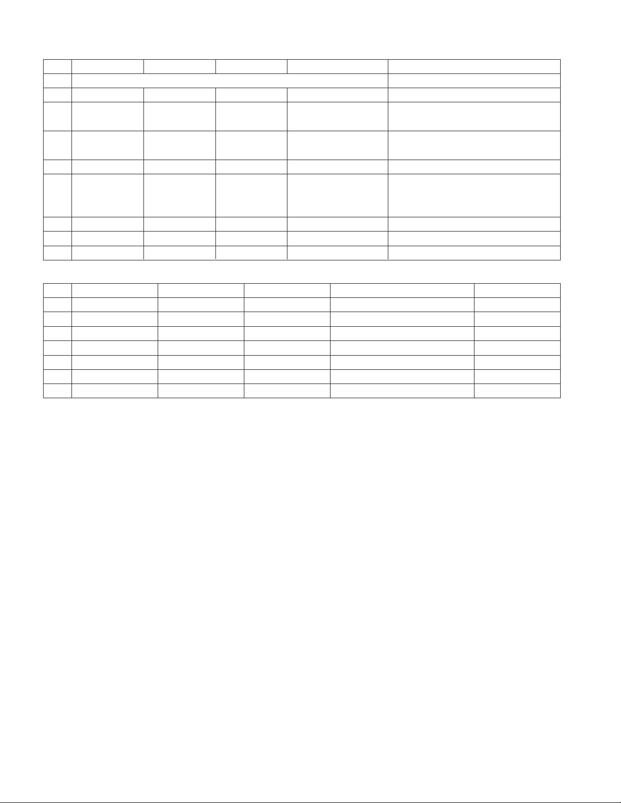
3.1. Setting up the LGIDS
1) Install the LGIDS
2) After installation, restart your PC.
3) Extract [files.zip] to folder [c:\LGIDS\files]
4) Start LGIDS.
3.2. Channel memory method
1) Press TILT key in Adjust remocon(Automatic setting).
2) Setting up like bottom figure
(Confirmation: Press ADJ Key in the Adjust remocon.
Select "System Control" by using D/E (CH+/-) key, and
press A (ENTER))
3) Connect RS232 cable .(Use the general RS-232C Twisted
Serial Cable).
4) Operate LGIDS
5) Select "Hurricane" and "ALL" on Model dialog and check
your connection in Communication dialog.
(If your connection is ‘NG’, then set your PORT(COM1,2,3,…)
correctly. If your connection has completed, you can see
)
6) Select proper CH_memory file(*.nvm) for each model at
[Channel Download] => [Write Batch].
Next, select proper binary file(*.bin) including the CH
information for each model at
[Channel Download] => [NVRAM File].
7) Click the [Download] button.
It means the completion of the CH memory download if all
items show 'OK' and Status is changed by 'PASS' at the
lower right corner of the window
4. Hudson Download
4.1 Hudson Download method
1) Press TILT key in Adjust remocon(Automatic setting).
2) Setting up like bottom figure
(Confirmation: Press ADJ Key in the Adjust remocon.
Select "System Control" by using D/E (CH+/-) key, and press
A (ENTER))
Ready
Page 11
LGE Internal Use OnlyCopyright © 2006 LG Electronics. Inc. All right reserved.
Only for training and service purposes
- 11 -
3) Connect RS232 cable(Use Download Jig and general RS232C Twisted Serial Cable).
*Before upgrading "Hudson flash memory", push the switch
on the download jig ‘inside’.
4) Operate LGIDS.
5) Select "Hurricane" and "ALL" on Model dialog and check
your connection in Communication dialog.
(If your connection is ‘NG’, then set your PORT (COM1, 2,
3,…) correctly. If your connection has completed, you can
see )
6) First, select proper Batch file(*.flm) for each model at [ROM
Download] => [Batch File].
Second, select proper RAM file(*.hex) for each model at
[ROM Download] => [RAM File].
Third, select roper Flash File(*.hex) for each model at
[ROM Download] => [Flash File].
7) Click the [Download] button.
It means the completion of the Hudson download if all
items show 'OK' and Status is changed by 'PASS' at the
lower right corner of the window.
Before AV ADC Calibration, should be executed the
"Panel size selection
5. Select method of Panel size
5.1 Press ADJ Key in the Adjust remocon
5.2 Select "Panel Control" by using
D/E (CH+/-) key, and
press
A (ENTER)
5.3 Select "Panel Size", and change the panel size among
32, 37, 42 according to the inch of model name.
(If the model name is 37LC2D-EC, change the Panel size
from default value to 37.)
5.4 After changing the panel size, push the EXIT Key
6. ADC Calibration
=> Caution: -System control RS-232 Host should be "PC" for
adjustment.
Before AV ADC Calibration, execute the "Panel size
selection"
Ready
ADC RF/AV/S-VIDEO Component RGB-PC
MSPG925F PAL Model:217 (720P) Model: 37
INPUT SELECT AV4 Pattern:33 (1024*768
Model: 202 (PAL-BGDHI) 720P/60Hz 100% 60Hz)
Pattern: 33 Color Bar Pattern: 33
PAL 100% Color Bar
Page 12

6.1 Adjustment of RF/AV/S-VIDEO
* Required Equipments
- Remote controller for adjustment
- MSPG-925F Pattern Generator (Which has Video Signal:
100% Color Bar Pattern shown in Fig. 1)
=> Model: 202 / Pattern: 33
Case1) EC and FC model use PAL-BGDHI (composite signal)
6.1.1 Method of Auto RF/AV/S-VIDEO Color Balance.
1) Input the Video Signal: 100% Color Bar signal into AV4
2) Set the PSM to Dynamic mode in the Picture menu
[Fig.1]
3) Press IN-START key on R/C for adjustment.
4) Press the G(Vol.+) key to operate the set, then it becomes
automatically.
5) Auto-RGB OK means the adjustment is completed.
6.2 Adjustment of Component.
* Required Equipments
- Remote controller for adjustment
- l MSPG-925F Pattern Generator => Model: 217/Pattern: 33
(Which has 720p/60Hz YPbPr output Pattern shown in Fig. 2 )
6.2.1 Method of Auto Component Color Balance
1) Input the Component 720p/60Hz 100% Color Bar(MSPG925F model:217, pattern:33) signal into Component.
2) Set the PSM to Dynamic mode in the Picture menu
[Fig.2]
3) Press the IN-START key on R/C for adjustment.
4) Press the G(Vol.+) key to operate the set , then it becomes
automatically.
5) Auto-RGB OK means the adjustment is completed.
6.3 Adjustment of RGB
* Required Equipments
- Remote controller for adjustment
-l MSPG-925F Pattern Generator
(Which has XGA [1024*768] 60Hz 100% Color Bar pattern
shown in Fig. 3)
6.3.1 Method of Auto RGB Color Balance
1) Input the PC 1024x768@60Hz 100% Color Bar pattern
(MSPG-925F model:37, pattern:33) into RGB.
(Using D-sub to D-sub cable)
2) Set the PSM to Dynamic mode in Picture menu.
3) Press the IN-START key on R/C for adjustment
[Fig.3]
4) Press the G(Vol.+) key operate To set , then it becomes
automatically.
5) Auto-RGB OK means adjustment is completed.
Before White-balance, the AV ADC should be done.
7. White Balance
=> Caution: - System control RS-232 Host should be "PC" for
adjustment.
- AV ADC should be done before White-balance.
* Test Equipment
Color Analyzer ( CA-110)
PC (for communication through RS-232C) => UART Baud
rate : 115200
Pattern Generator (MSPG-925F)
* Target Value (PSM: Dynamic, CSM: Normal)
- Normal(9300K) x:0.283±0.003, y: 0.298±0.003
- Luminance(Y) AV/COMP: 250 Cd/m2 (Typ: 300 Cd/m2)
PC : 300 Cd/m2 (Typ: 350 Cd/m2)
-> Reference Value(Automatically fixed)
- Cool(11000K) - x: 0.274±0.003, y: 0.286±0.003
- Warm(7200K) - x:0.303±0.003, y: 0.319±0.003
- 12 -
LGE Internal Use OnlyCopyright © 2006 LG Electronics. Inc. All right reserved.
Only for training and service purposes
White balance AV4
MSPG925F High Model : 202
*239Gray Pattern : 47
*Pal Video
Page 13

LGE Internal Use OnlyCopyright © 2006 LG Electronics. Inc. All right reserved.
Only for training and service purposes
- 13 -
6. Shipping Conditions
No Item Condition Remark
1 Power Off
2 Volume Level 30
3 Main Picture Input TV
4 Main Last Channel Pr 01
5 Mute Off
6 ARC 16 : 9
7 Station Auto Program
Manual Program
Program Edit
Favorite Program None
8 Picture PSM Dynamic
Dynamic Contrast 100
Brightness 45
Colour 50
Sharpness 50
CSM Normal ZE(TE)
XD On
ACM Fleshtone : 1
Greentone : 1
Bluetone : 1
9 Sound SSM Flat
BBE Off
AVL Off
Balance 0
Treble 50
Bass 50
TV Speaker On
10 Time Clock -- : -- User control
Off time Off
On time On
Auto sleep Off
11 Special Language English
Area Management
Child Lock Off
Set ID 1
XD Demo To Start
Logo light On
Index On
12 Screen Auto config
Manual config
XGA Mode
ARC
Zoom +/- Variable by each mode
Position
Cinema
NR
Reset
Page 14

LGE Internal Use OnlyCopyright © 2006 LG Electronics. Inc. All right reserved.
Only for training and service purposes
- 14 -
TROUBLESHOOTING
No image
Push the POWER
ON key
Check for S/W error
Replace Cortez
Replace Hudson
Power Error
Replace CXA2069
Correct the circuit
Attach the input
cable(s)
Change the Tuner
Correct the circuit
RF
Power Error
Is the Set ON?
Is the input
cable attached?
What is
the input signal
mode?
Check Vout
Signal at pin 9.
Of Tuner
Check 33V
And 5V at pin
7,6 resp. of
Tuner
Check Vout
Signal at C230
Check Sub_V
At R302
Check Main_V
At R309
Check 24bit
RGB at AR700-
AR705
Check LVDS
Output of Cortez
Check Power
Levels and crystal
Check Q303
Circuit and 9V
at L300
Check the
Condition of all
Connectors, wafers,
I2C In the
system.
YES
NO
NO
YES
PASS
FAIL
FAIL
PASS
PASS
FAIL
PASS
PASS
PASS
PASS
FAIL
FAIL
PASS
FAIL
FAIL
PASS
FAIL
Page 15

LGE Internal Use OnlyCopyright © 2006 LG Electronics. Inc. All right reserved.
Only for training and service purposes
- 15 -
No image
Push the POWER
ON key
Check for S/W error
Replace Cortez
Replace Hudson
Power Error
Replace CXA2069
Correct the circuit
Attach the input
cable(s)
Replace Jack board
AV1
Power Error
Check the
Condition of all
Connectors, wafers,
I2C In the
system.
Check CVBS
Signal at R103
of jack board
Check 3.3V
At L110 on jack
board
Check Sub_V
At R302
Check Main_V
At R309
Check 24bit
RGB at AR700-
AR705
Check LVDS
Output of Cortez
Check Power
Levels and crystal
Check Q303
Circuit and 9V
at L300
Is the
Set ON?
Is the input
cable attached?
What is
the input signal
mode?
YES
NO
YES
PASS
FAIL
FAIL
PASSPASS
PASS
PASS
PASS
FAIL
FAIL FAIL
PASS
FAIL
FAIL
PASS
NO
Page 16

LGE Internal Use OnlyCopyright © 2006 LG Electronics. Inc. All right reserved.
Only for training and service purposes
- 16 -
No image
Push the POWER
ON key
Check for S/W error
Replace Cortez
Replace Hudson
Power Error
Replace CXA2069
Correct the circuit
Attach the input
cable(s)
Replace Jack board
AV2
Power Error
Check the
Condition of all
Connectors, wafers,
I2C In the
system.
Check CVBS
Signal at R105
of jack board
Check 3.3V
At L110 on jack
board
Check Sub_V
At R302
Check Main_V
At R309
Check 24bit
RGB at AR700-
AR705
Check LVDS
Output of Cortez
Check Power
Levels and crystal
Check Q303
Circuit and 9V
at L300
Is the
Set ON?
Is the input cable
attached?
What is
the input signal
mode?
YES
NO
NO
YES
PASS
FAIL
FAIL
PASS
PASS
FAIL
PASS
PASS
PASS
FAIL
PASS
FAIL
FAIL
PASS
FAIL
Page 17

LGE Internal Use OnlyCopyright © 2006 LG Electronics. Inc. All right reserved.
Only for training and service purposes
- 17 -
No image
Push the POWER
ON key
Check for S/W error
Replace Cortez
Replace Hudson
Power Error
Replace CXA2069
Correct the circuit
Attach the input
cable(s)
Replace Jack board
AV3
Power Error
Check the
Condition of all
Connectors, wafers,
I2C In the
system.
Is the
Set ON?
Is the input cable
attached?
What is
the input signal
mode?
Check CVBS
Signal at R144
of jack board
Check 3.3V
At L110 on jack
board
Check Sub_V
At R302
Check Main_V
At R309
Check 24bit
RGB at AR700-
AR705
Check LVDS
Output of Cortez
Check Power
Levels and crystal
Check Q303
Circuit and 9V
at L300
YES
NO
NO YES
PASS
FAIL
FAIL
PASS
PASS
FAIL
PASS
FAIL
FAIL
PASS
FAIL
FAIL
PASS
PASS
PASS
Page 18

LGE Internal Use OnlyCopyright © 2006 LG Electronics. Inc. All right reserved.
Only for training and service purposes
- 18 -
No image
Push the POWER
ON key
Check for S/W error
Replace Cortez
Replace Hudson
Power Error
Replace CXA2069
Correct the circuit
Attach the input
cable(s)
Replace Jack Board
S-Video
Power Error
Check the
Condition of all
Connectors, wafers,
I2C In the
system.
Check Y/C
Signal at L131,132 on
Jack board
Check 3.3V
At L110 on jack
board
Check Sub_YC
At R302,303
Check Main_YC
At R309,320
Check 24bit
RGB at AR700-
AR705
Check LVDS
Output of Cortez
Check Power
Levels and crystal
Check Q303
Circuit and 9V
at L300
Is the input cable
attached?
Is the
Set ON?
What is
the input signal
mode?
YES
NO
NO
YES
PASS
FAIL
FAIL
PASS
PASS
FAIL
FAIL
PASS
FAIL
PASS
FAIL
PASS
PASS
PASS
FAIL
Page 19

LGE Internal Use OnlyCopyright © 2006 LG Electronics. Inc. All right reserved.
Only for training and service purposes
- 19 -
No image
Push the POWER
ON key
Check for S/W error
Replace Cortez
Replace Hudson
Power Error
Replace CXA2069
Correct the circuit
Attach the input
cable(s)
Replace Jack Board
AV4
Power Error
Check the
Condition of all
Connectors, wafers,
I2C In the
system.
Check CVBS
Signal at R169
on jack board
Check 3.3V
At L110 on jack
board
Check Sub_V
At R302
Check Main_V
At R309
Check 24bit
RGB at AR700-
AR705
Check LVDS
Output of Cortez
Check Power
Levels and crystal
Check Q303
Circuit and 9V
at L300
What is
the input signal
mode?
Is the input cable
attached?
Is the
Set ON?
YES NO
NO
YES
PASS
FAIL
PASS
FAIL
PASS
PASS
PASS
PASS
FAIL
FAIL
PASS
FAIL
PASS
FAIL
FAIL
Page 20

LGE Internal Use OnlyCopyright © 2006 LG Electronics. Inc. All right reserved.
Only for training and service purposes
- 20 -
No image
Push the POWER
ON key
Check for S/W error
Replace Cortez
Replace Hudson
Power Error
Replace IC505
Replace STi5100
Power Error
Attach the input
cable(s)
Replace Tuner
DTV
Power Error
Check the
Condition of all
Connectors, wafers,
I2C In the
system.
Check 8bit
Signal at digital
Tuner at
R318-326.
Check 5V
At L305,310
Check 8bit
Signal at AR110-
AR111
Check 8bit
Signal at AR 500-
AR501
Check 24bit
RGB at AR700-
AR705
Check LVDS
Output of Cortez
Check Power
Levels and crystal
Check power
Levels for
STi5100
Is the
Set ON
Is the input
cable attached?
What is
the input signal
mode?
YES
NO
NO
YES
PASS
FAIL
PASS
FAIL
PASS
FAIL
PASS
FAIL
FAIL
FAIL
FAIL
PASS
PASS
PASS
PASS
FAIL
PASS
Page 21

LGE Internal Use OnlyCopyright © 2006 LG Electronics. Inc. All right reserved.
Only for training and service purposes
- 21 -
No image
Push the POWER
ON key
Check for S/W error
Replace Cortez
Replace Hudson
Power Error
Replace IC301
Power Error
Attach the input
cable(s)
Replace Jack Board
Component
Power Error
Check the
Condition of all
Connectors, wafers,
I2C In the
system.
Check Y,Pb,Pr
At L129,128,130
respectively
Check 3.3V
At L110 on jack
board
Check Sync_DE
Signal at R370
Check 24bit
RGB at AR700-
AR705
Check LVDS
Output of Cortez
Check Power
Levels and crystal
Check 5V
At L303 on jack
board
Is the
Set ON?
Is the input cable
attached?
What is
the input signal
mode?
YES
NO
NO
YES
PASS
FAIL
FAIL
PASS
FAIL
FAIL
FAIL
PASS
FAIL
PASS
PASS
PASS
PASS
PASS
FAIL
Page 22

LGE Internal Use OnlyCopyright © 2006 LG Electronics. Inc. All right reserved.
Only for training and service purposes
- 22 -
No image
Push the POWER
ON key
Check for S/W error
Replace Cortez
Replace Hudson
Power Error
Power Error
Replace Jack Board
Attach the input
cable(s)
RGB
Check the
Condition of all
Connectors, wafers,
I2C In the
system.
Is the
Set ON?
Is the input
cable attached?
What is
the input signal
mode?
Check LVDS
Output of Cortez
Check 24bit
RGB at AR700-
AR705
Check RGB
HV signal at R513
512,509,510,515
On Jack board
Check 3.3V
At L500 on jack
board
Check Power
Levels and crystal
YES
NO
NO
YES
PASS
PASS
FAIL
FAIL
FAILPASSPASS
PASS
FAIL
FAIL
FAIL
PASS
Page 23

LGE Internal Use OnlyCopyright © 2006 LG Electronics. Inc. All right reserved.
Only for training and service purposes
- 23 -
No image
Push the POWER
ON key
Check for S/W error
Replace Cortez
Replace Hudson
Power Error
Power Error
Replace SiI9011
Attach the input
cable(s)
Check outside
connections
HDMI
Power Error
Check the
Condition of all
Connectors, wafers,
I2C In the
system.
Check TMDS
Signal at AR1206-7
on main board
Check 5V
At R1232 on
Main board
Check 24 bit
RGB signal at
AR1200-1205
Check 24bit
RGB at AR700-
AR705
Check LVDS
Output of Cortez
Check Power
Levels and crystal
Check 1.8V
At L1206 and 3.3V at
L1207 And
crystal
Is the
Set ON?
Is the input cable
attached?
What is
the input signal
mode?
YES
NO
NO
YES
PASS
FAIL
PASS
FAIL
PASS
FAIL
PASS
FAIL
PASS
FAIL
FAIL
FAIL
PASS
PASS PASS
Page 24

LGE Internal Use OnlyCopyright © 2006 LG Electronics. Inc. All right reserved.
Only for training and service purposes
- 24 -
No Audio
Push the POWER
ON key
Replace the MSP
Power error or
replace CXA2069
Power Error
Check the interfacing circuit
of
AV1,2,3 and AV4/S-Video
Check
the Condition
of all Connectors,
wafers, I2C In
corresponding
Signal
flow?
Check the
supply voltage 8V
across L403
Check the
AV L/R output
At R377,376
Check
audio output at MSP
across R429-431.
Is the
Set ON?
YES
Turn OFF the Mute
Is the
Mute ON?
Check the
PWM output of NSP
across R436-439
Check
3.3V supply across
L402 and 1.8V at
C448
Check the
Amplifier output level
At L423-426
Check 18V
supply at L421
Increase the Volume
Is
Volume level Of
the set 0?
Check the
AV1,AV2 ,AV3,
AV4/S-Video L/R signal
across R136-138, R135-137,
R157-158, R174-175 respectively
according to the
corresponding mode
On jack board
Correct them
Replace NSP
Power Error
Replace
TAS5122(amp)
There may be some
error in Audio
source.
TROUBLESHOOTING AV1, 2, 3, 4/S-Video
Page 25

LGE Internal Use OnlyCopyright © 2006 LG Electronics. Inc. All right reserved.
Only for training and service purposes
- 25 -
No Audio
Push the POWER
ON key
Replace the MSP
Power error or
replace
IC605(TC74LCX157)
Power Error
Check the interfacing circuit
of
HDMI or replace STi5100
Check
the Condition
of all Connectors,
wafers, I2C In
corresponding
Signal flow?
Check the
supply voltage 8V
across L403
Check the
MUX I2S output
At R491,493,494 On
jack board
Check audio
output at MSP across
R429-431.
Check the
PWM output of
NSP across
R436-439
Check the
Amplifier output level
At L423-426
Check 18V
supply at L421
Check
3.3V supply across
L402 and 1.8V at
C448
Is the
Set ON?
Check the DTV
HDMI I2S signal at R183,
184,186 and R1218-1220
respectively according to The
corresponding mode On
main board
YES
Turn OFF the Mute
Is the
Mute ON?
Increase the Volume
Is
Volume level Of
the set?
Correct them
Replace NSP
Power Error
Replace
TAS5122(amp)
There may be some
error in Audio
source.
TROUBLESHOOTING DTV/HDMI-Audio
Page 26

LGE Internal Use OnlyCopyright © 2006 LG Electronics. Inc. All right reserved.
Only for training and service purposes
- 26 -
No Audio
Push the POWER
ON key
Replace the MSP
Power Error
Check the interfacing circuit
of Analog Tuner, component
and PC audio accordingly
w.r.t the mode.
Check the
Condition of all
Connectors, wafers,
I2C In corresponding
Signal flow?
Check the
supply voltage 8V
across L403
Check audio
output at MSP across
R429-431.
Check
the PWM output
of NSP across
R436-439
Check
3.3V supply across
L402 and 1.8V at
C448
Check 18V
supply at L421
Check the
Amplifier output level
at L423-426
Is the
Set ON?
Check
the RF SIF,
Component L/R and
PC L/R signal across R212,
R171-170, R505-506,
respectively according to
the corresponding
mode on jac
board
YES
Turn OFF the Mute
Is the
Mute ON?
Increase the Volume
Is Volume level
of the set 0?
Correct them
Replace NSP.
Power Error
Replace
TAS5122(amp)
There may be some
error in Audio
source.
TROUBLESHOOTING RF/Component/PC
Page 27

BLOCK DIAGRAM(Main)
- 27 -
LGE Internal Use OnlyCopyright © 2006 LG Electronics. Inc. All right reserved.
Only for training and service purposes
TDFB-G236P
DVB/PAL
8bit(656),27M Hz,I2S
STi5100
CI SLOT
TS IN
CI TS
74LCX244
Tuner TS
MUX
3 State Buffer
3state-cont rol
SPDIF out
8bit(656),27M Hz,I2S
DTV out VLR
FFC WaferFFC Wafer FFC Wafer
Cortez Hudson
Sub V/YC
Main V/YC
8Pin Record
PC_RGB
Comp YPbPr
Scart RGB
Sil9012
TMDS Rx
(HDCP)
HDMI
8bit
SPDIF OUT
24bit
24bit
SPDIF out DTV
SPDIF out MSP
24bit
24bit
DTV out VLR
LVDS_31P
LCD : 10bit, AI, PWM,
INV_BRI
24bit
Uart commu nic ation
Uart commu nic ation
24bit
PDP modul e D/L
SDA,SCL
Wafer to PDP modul e
PDF Fan
Fan Contro l
Page 28

LGE Internal Use OnlyCopyright © 2006 LG Electronics. Inc. All right reserved.
Only for training and service purposes
- 28 -
BLOCK DIAGRAM(Jack)
CXA2069Q
AUDIO/VI DEO SW
MSP4410K
Sound processor
NSP-2110A
Digital s ound processor
VLR
TV_out V
SCART RGB
VLR, YC
DTV V_out
MNT_VLR
PC_RGB
YPbPr
Component Jack
Audio_LR
WIRE_IR_in
WIRE_IR_out
Audi o out
CVBS
Audio
TV_out L R
I2S
Digital AMP
I2S DTV/HDMI
Main V/YC
AV_LR
AV1
DTV out
AV2
RGB
audio
RGB in
IR
out
IR
In
AV3
Side AV
VLR
LR
VLR, YC
Sub V/YC
EPF LR
Audio_LR
TV_LR
MSP_SPDIF
8Pin Record
8Pin Record
FFC WaferFFC Wafer FFC Wafer
Page 29

- 29 -
LGE Internal Use OnlyCopyright LG Electronics. Inc. All right reserved.
Only for training and service purposes
EXPLODED VIEW
010
020
080
120
140
090
150
030
070
170
110
050
050
060
100
040
130
Many electrical and mechanical parts in this chassis have special safety-related characteristics. These
parts are identified by in the Schematic Diagram and EXPLODED VIEW.
It is essential that these special safety parts should be replaced with the same components as
recommended in this manual to prevent X-RADIATION, Shock, Fire, or other Hazards.
Do not modify the original design without permission of manufacturer.
IMPORTANT SAFETY NOTICE
Page 30

Page 31

Page 32

Page 33

Page 34

Page 35

Jun., 2006
Printed in KoreaP/NO : MFL36666002
 Loading...