

LG 32LH70YD-SH Schematic
LCD TV
SERVICE MANUAL
CAUTION
BEFORE SERVICING THE CHASSIS,
READ THE SAFETY PRECAUTIONS IN THIS MANUAL.
CHASSIS : LJ91D
MODEL : 32LH70YD
32LH70YD-SH
North/Latin America http://aic.lgservice.com
Europe/Africa http://eic.lgservice.com
Asia/Oceania http://biz.lgservice.com
Internal Use Only
Printed in KoreaP/NO : MFL61862402 (0905-REV01)

LGE Internal Use OnlyCopyright LG Electronics. Inc. All right reserved.
Only for training and service purposes
- 2 -
CONTENTS
CONTENTS .............................................................................................. 2
PRODUCT SAFETY ..................................................................................3
SPECIFICATION........................................................................................6
ADJUSTMENT INSTRUCTION ...............................................................14
TROUBLE SHOOTING............................................................................17
BLOCK DIAGRAM...................................................................................58
EXPLODED VIEW .................................................................................. 59
SVC. SHEET ...............................................................................................
LGE Internal Use OnlyCopyright LG Electronics. Inc. All right reserved.
Only for training and service purposes
- 3 -
SAFETY PRECAUTIONS
Many electrical and mechanical parts in this chassis have special safety-related characteristics. These parts are identified by in the
Schematic Diagram and Exploded View.
It is essential that these special safety parts should be replaced with the same components as recommended in this manual to prevent
Shock, Fire, or other Hazards.
Do not modify the original design without permission of manufacturer.
General Guidance
An isolation Transformer should always be used during the
servicing of a receiver whose chassis is not isolated from the AC
power line. Use a transformer of adequate power rating as this
protects the technician from accidents resulting in personal injury
from electrical shocks.
It will also protect the receiver and it's components from being
damaged by accidental shorts of the circuitry that may be
inadvertently introduced during the service operation.
If any fuse (or Fusible Resistor) in this TV receiver is blown,
replace it with the specified.
When replacing a high wattage resistor (Oxide Metal Film Resistor,
over 1W), keep the resistor 10mm away from PCB.
Keep wires away from high voltage or high temperature parts.
Before returning the receiver to the customer,
always perform an AC leakage current check on the exposed
metallic parts of the cabinet, such as antennas, terminals, etc., to
be sure the set is safe to operate without damage of electrical
shock.
Leakage Current Cold Check(Antenna Cold Check)
With the instrument AC plug removed from AC source, connect an
electrical jumper across the two AC plug prongs. Place the AC
switch in the on position, connect one lead of ohm-meter to the AC
plug prongs tied together and touch other ohm-meter lead in turn to
each exposed metallic parts such as antenna terminals, phone
jacks, etc.
If the exposed metallic part has a return path to the chassis, the
measured resistance should be between 1MΩ and 5.2MΩ.
When the exposed metal has no return path to the chassis the
reading must be infinite.
An other abnormality exists that must be corrected before the
receiver is returned to the customer.
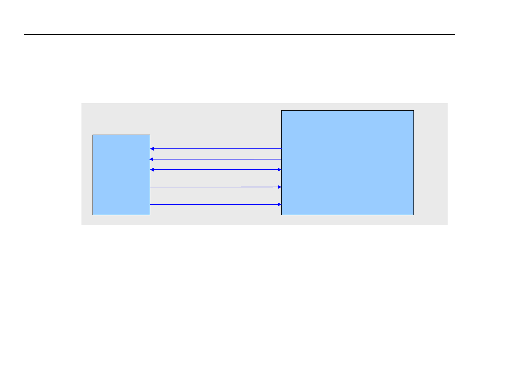
Leakage Current Hot Check (See below Figure)
Plug the AC cord directly into the AC outlet.
Do not use a line Isolation Transformer during this check.
Connect 1.5K/10watt resistor in parallel with a 0.15uF capacitor
between a known good earth ground (Water Pipe, Conduit, etc.)
and the exposed metallic parts.
Measure the AC voltage across the resistor using AC voltmeter
with 1000 ohms/volt or more sensitivity.
Reverse plug the AC cord into the AC outlet and repeat AC voltage
measurements for each exposed metallic part. Any voltage
measured must not exceed 0.75 volt RMS which is corresponds to
0.5mA.
In case any measurement is out of the limits specified, there is
possibility of shock hazard and the set must be checked and
repaired before it is returned to the customer.
Leakage Current Hot Check circuit
1.5 Kohm/10W
To Instrument’s
exposed
METALLIC PARTS
Good Earth Ground
such as WATER PIPE,
CONDUIT etc.
AC Volt-meter
When 25A is impressed between Earth and 2nd Ground
for 1 second, Resistance must be less than 0.1
*Base on Adjustment standard
IMPORTANT SAFETY NOTICE
0.15uF
Ω

LGE Internal Use OnlyCopyright LG Electronics. Inc. All right reserved.
Only for training and service purposes
- 4 -
CAUTION: Before servicing receivers covered by this service
manual and its supplements and addenda, read and follow the
SAFETY PRECAUTIONS on page 3 of this publication.
NOTE: If unforeseen circumstances create conflict between the
following servicing precautions and any of the safety precautions on
page 3 of this publication, always follow the safety precautions.
Remember: Safety First.
General Servicing Precautions
1. Always unplug the receiver AC power cord from the AC power
source before;
a. Removing or reinstalling any component, circuit board
module or any other receiver assembly.
b. Disconnecting or reconnecting any receiver electrical plug or
other electrical connection.
c. Connecting a test substitute in parallel with an electrolytic
capacitor in the receiver.
CAUTION: A wrong part substitution or incorrect polarity
installation of electrolytic capacitors may result in an
explosion hazard.
2. Test high voltage only by measuring it with an appropriate high
voltage meter or other voltage measuring device (DVM,
FETVOM, etc) equipped with a suitable high voltage probe.
Do not test high voltage by "drawing an arc".
3. Do not spray chemicals on or near this receiver or any of its
assemblies.
4. Unless specified otherwise in this service manual, clean
electrical contacts only by applying the following mixture to the
contacts with a pipe cleaner, cotton-tipped stick or comparable
non-abrasive applicator; 10% (by volume) Acetone and 90% (by
volume) isopropyl alcohol (90%-99% strength)
CAUTION: This is a flammable mixture.
Unless specified otherwise in this service manual, lubrication of
contacts in not required.
5. Do not defeat any plug/socket B+ voltage interlocks with which
receivers covered by this service manual might be equipped.
6. Do not apply AC power to this instrument and/or any of its
electrical assemblies unless all solid-state device heat sinks are
correctly installed.
7. Always connect the test receiver ground lead to the receiver
chassis ground before connecting the test receiver positive
lead.
Always remove the test receiver ground lead last.
8. Use with this receiver only the test fixtures specified in this
service manual.
CAUTION: Do not connect the test fixture ground strap to any
heat sink in this receiver.
Electrostatically Sensitive (ES) Devices
Some semiconductor (solid-state) devices can be damaged easily
by static electricity. Such components commonly are called
Electrostatically Sensitive (ES) Devices. Examples of typical ES
devices are integrated circuits and some field-effect transistors and
semiconductor "chip" components. The following techniques
should be used to help reduce the incidence of component
damage caused by static by static electricity.
1. Immediately before handling any semiconductor component or
semiconductor-equipped assembly, drain off any electrostatic
charge on your body by touching a known earth ground.
Alternatively, obtain and wear a commercially available
discharging wrist strap device, which should be removed to
prevent potential shock reasons prior to applying power to the
unit under test.
2. After removing an electrical assembly equipped with ES
devices, place the assembly on a conductive surface such as
aluminum foil, to prevent electrostatic charge buildup or
exposure of the assembly.
3. Use only a grounded-tip soldering iron to solder or unsolder ES
devices.
4. Use only an anti-static type solder removal device. Some solder
removal devices not classified as "anti-static" can generate
electrical charges sufficient to damage ES devices.
5. Do not use freon-propelled chemicals. These can generate
electrical charges sufficient to damage ES devices.
6. Do not remove a replacement ES device from its protective
package until immediately before you are ready to install it.
(Most replacement ES devices are packaged with leads
electrically shorted together by conductive foam, aluminum foil
or comparable conductive material).
7. Immediately before removing the protective material from the
leads of a replacement ES device, touch the protective material
to the chassis or circuit assembly into which the device will be
installed.
CAUTION: Be sure no power is applied to the chassis or circuit,
and observe all other safety precautions.
8. Minimize bodily motions when handling unpackaged
replacement ES devices. (Otherwise harmless motion such as
the brushing together of your clothes fabric or the lifting of your
foot from a carpeted floor can generate static electricity
sufficient to damage an ES device.)
General Soldering Guidelines
1. Use a grounded-tip, low-wattage soldering iron and appropriate
tip size and shape that will maintain tip temperature within the
range or 500
°F to 600°F.
2. Use an appropriate gauge of RMA resin-core solder composed
of 60 parts tin/40 parts lead.
3. Keep the soldering iron tip clean and well tinned.
4. Thoroughly clean the surfaces to be soldered. Use a mall wirebristle (0.5 inch, or 1.25cm) brush with a metal handle.
Do not use freon-propelled spray-on cleaners.
5. Use the following unsoldering technique
a. Allow the soldering iron tip to reach normal temperature.
(500
°F to 600°F)
b. Heat the component lead until the solder melts.
c. Quickly draw the melted solder with an anti-static, suction-
type solder removal device or with solder braid.
CAUTION: Work quickly to avoid overheating the circuit
board printed foil.
6. Use the following soldering technique.
a. Allow the soldering iron tip to reach a normal temperature
(500
°F to 600°F)
b. First, hold the soldering iron tip and solder the strand against
the component lead until the solder melts.
c. Quickly move the soldering iron tip to the junction of the
component lead and the printed circuit foil, and hold it there
only until the solder flows onto and around both the
component lead and the foil.
CAUTION: Work quickly to avoid overheating the circuit
board printed foil.
d. Closely inspect the solder area and remove any excess or
splashed solder with a small wire-bristle brush.
SERVICING PRECAUTIONS

LGE Internal Use OnlyCopyright LG Electronics. Inc. All right reserved.
Only for training and service purposes
- 5 -
IC Remove/Replacement
Some chassis circuit boards have slotted holes (oblong) through
which the IC leads are inserted and then bent flat against the
circuit foil. When holes are the slotted type, the following technique
should be used to remove and replace the IC. When working with
boards using the familiar round hole, use the standard technique
as outlined in paragraphs 5 and 6 above.
Removal
1. Desolder and straighten each IC lead in one operation by gently
prying up on the lead with the soldering iron tip as the solder
melts.
2. Draw away the melted solder with an anti-static suction-type
solder removal device (or with solder braid) before removing the
IC.
Replacement
1. Carefully insert the replacement IC in the circuit board.
2. Carefully bend each IC lead against the circuit foil pad and
solder it.
3. Clean the soldered areas with a small wire-bristle brush.
(It is not necessary to reapply acrylic coating to the areas).
"Small-Signal" Discrete Transistor
Removal/Replacement
1. Remove the defective transistor by clipping its leads as close as
possible to the component body.
2. Bend into a "U" shape the end of each of three leads remaining
on the circuit board.
3. Bend into a "U" shape the replacement transistor leads.
4. Connect the replacement transistor leads to the corresponding
leads extending from the circuit board and crimp the "U" with
long nose pliers to insure metal to metal contact then solder
each connection.
Power Output, Transistor Device
Removal/Replacement
1. Heat and remove all solder from around the transistor leads.
2. Remove the heat sink mounting screw (if so equipped).
3. Carefully remove the transistor from the heat sink of the circuit
board.
4. Insert new transistor in the circuit board.
5. Solder each transistor lead, and clip off excess lead.
6. Replace heat sink.
Diode Removal/Replacement
1. Remove defective diode by clipping its leads as close as
possible to diode body.
2. Bend the two remaining leads perpendicular y to the circuit
board.
3. Observing diode polarity, wrap each lead of the new diode
around the corresponding lead on the circuit board.
4. Securely crimp each connection and solder it.
5. Inspect (on the circuit board copper side) the solder joints of
the two "original" leads. If they are not shiny, reheat them and if
necessary, apply additional solder.
Fuse and Conventional Resistor
Removal/Replacement
1. Clip each fuse or resistor lead at top of the circuit board hollow
stake.
2. Securely crimp the leads of replacement component around
notch at stake top.
3. Solder the connections.
CAUTION: Maintain original spacing between the replaced
component and adjacent components and the circuit board to
prevent excessive component temperatures.
Circuit Board Foil Repair
Excessive heat applied to the copper foil of any printed circuit
board will weaken the adhesive that bonds the foil to the circuit
board causing the foil to separate from or "lift-off" the board. The
following guidelines and procedures should be followed whenever
this condition is encountered.
At IC Connections
To repair a defective copper pattern at IC connections use the
following procedure to install a jumper wire on the copper pattern
side of the circuit board. (Use this technique only on IC
connections).
1. Carefully remove the damaged copper pattern with a sharp
knife. (Remove only as much copper as absolutely necessary).
2. carefully scratch away the solder resist and acrylic coating (if
used) from the end of the remaining copper pattern.
3. Bend a small "U" in one end of a small gauge jumper wire and
carefully crimp it around the IC pin. Solder the IC connection.
4. Route the jumper wire along the path of the out-away copper
pattern and let it overlap the previously scraped end of the good
copper pattern. Solder the overlapped area and clip off any
excess jumper wire.
At Other Connections
Use the following technique to repair the defective copper pattern
at connections other than IC Pins. This technique involves the
installation of a jumper wire on the component side of the circuit
board.
1. Remove the defective copper pattern with a sharp knife.
Remove at least 1/4 inch of copper, to ensure that a hazardous
condition will not exist if the jumper wire opens.
2. Trace along the copper pattern from both sides of the pattern
break and locate the nearest component that is directly
connected to the affected copper pattern.
3. Connect insulated 20-gauge jumper wire from the lead of the
nearest component on one side of the pattern break to the lead
of the nearest component on the other side.
Carefully crimp and solder the connections.
CAUTION: Be sure the insulated jumper wire is dressed so the
it does not touch components or sharp edges.
LGE Internal Use OnlyCopyright LG Electronics. Inc. All right reserved.
Only for training and service purposes
- 6 -
SPECIFICATION
NOTE : Specifications and others are subject to change without notice for improvement
.
4. Electrical specification
4.1 General Specification
1. Application range
This specification is applied to the LCD TV used LJ91D
chassis.
2. Requirement for Test
Each part is tested as below without special appointment.
1) Temperature : 25±5ºC (77±9ºF), CST : 40±5ºC
2) Relative Humidity : 65±10%
3)
Power Voltage : Standard input voltage(100~240V@50/60Hz)
* Standard Voltage of each products is marked by models.
4) Specification and performance of each parts are followed
each drawing and specification by part number in
accordance with BOM.
5) The receiver must be operated for about 5 minutes prior to
the adjustment.
3. Test method
1) Performance: LGE TV test method followed
2) Demanded other specification
- Safety: CE, IEC specification
- EMC: CE, IEC specification
No Item Specification Remark
1.
Receiving System
1) SBTVD / NTSC / PAL-M / PAL-N
2.
Available Channel 1) VHF : 02~13
2) UHF : 14~69
3) DTV : 02-69
4) CATV : 01~135
3. Input Voltage 1) AC 100 ~ 240V 50/60Hz Mark : 110V, 60Hz
4. Market Cent
32 inch Wide(1920x1080)
42 inch Wide(1920x1080)
47 inch Wide(1920x1080)
LC320WUD-SBA1(Vitaz 4)
LC420WUD-SBT1(Vitaz 4)
LC470WUD-SAT1(Vitaz 4)
32LH70YD-SH
42LH70YD-SE
47LH70YD-SE
32LH70YD-SH
42LH70YD-SE
47LH70YD-SE
ral and South AMERICA
5.
Screen Size
6. Aspect Ratio 16:9
7. Tuning System FS
8.
Module
9.
Operating Environment 1) Temp : 0 ~ 40 deg
2) Humidity : ~ 80 %
10.
Storage Environment 1) Temp : -20 ~ 60 deg
2) Humidity : ~ 85 %

- 7 -
LGE Internal Use OnlyCopyright LG Electronics. Inc. All right reserved.
Only for training and service purposes
5. Chromiance & Luminance spec.
No
32LH70YD-SH
Item Min Typ Max Unit Remark
Module cd/m 1. Max Luminance
(Center 1-point / Full White
Pattern)
Set
400 500
400 500 cd/m
2. 3.Luminance uniformity 77 % Full white
0.638
0.334
4.
5.
RED
0.291
0.607
6.
7.
GREEN
0.145
0.062
8.
9.
BLUE
0.279
10.
Color
coordinate
WHITE
Y
X
Y
X
Y
X
Y
X
Typ.
-0.03
0.292
Typ.
+0.03
11. Color coordinate uniformity N/A
900:1 1300:1 NORMAL
Contrast ratio
50000:1 80000:1 DCR
Cool
0.281
0.274
0.276
0.283
0.278
0.285
Standard
0.291
0.283
0.311
0.285
0.293
0.287
0.295
12. Color
Temperature
Warm
0.327
0.313
0.329
0.315
0.331
<Test Condition>
85% Full white pattern
** The W/B Tolerance is
–0.015 for Adjustment
Dynamic contrast : off
Dynamic color : off
OPC : off
13. Color Distortion, DG 10.0 %
14. Color Distortion, DP 10.0 deg
15. Color S/N, AM/FM 43.0 dB
16. Color Killer Sensitivity -80 dBm
6. Component Input (Y, C
B/PB, CR/PR)
No Resolution H-freq(kHz) V-freq.(kHz) Pixel clock Proposed
1. 720*480 15.73 60 13.5135 SDTV ,DVD 480I
2. 720*480 15.73 59.94 13.5 SDTV ,DVD 480I
3. 720*480 31.47 60 27.027 SDTV 480P
4. 720*480 31.47 59.94 27.0 SDTV 480P
5. 1280*720 45.00 60.00 74.25 HDTV 720P
6. 1280*720 44.96 59.94 74.176 HDTV 720P
7. 1920*1080 33.75 60.00 74.25 HDTV 1080I
8. 1920*1080 33.72 59.94 74.176 HDTV 1080I
9. 1920*1080 67.500 60 148.50 HDTV 1080P
10. 1920*1080 67.432 59.939 148.352 HDTV 1080P
11. 1920*1080 27.000 24.000 74.25 HDTV 1080P
12. 1920*1080 26.97 23.94 74.176 HDTV 1080P
13. 1920*1080 33.75 30.000 74.25 HDTV 1080P
14. 1920*1080 33.71 29.97 74.176 HDTV 1080P
15. 1920*1080 56.25 50.000 148.5 HDTV 1080P
16. 1920*1080 28.125 25.000 74.25 HDTV 1080P
- 8 -
LGE Internal Use OnlyCopyright LG Electronics. Inc. All right reserved.
Only for training and service purposes
7. RGB Input (PC)
No Resolution H-freq(kHz) V-freq.(Hz) Pixel clock(MHz) Proposed
PC DDC
1. 640*350 31.468 70.09 25.17 EGA X
O
O
O
O
O
O
O
O
O
O
2. 720*400 31.469 70.08 28.32 DOS
3. 640*480 31.469 59.94 25.17 VESA(VGA)
4. 800*600 35.156 56.25 36.00 VESA(SVGA)
5. 800*600 37.879 60.31 40.00 VESA(SVGA)
6. 1024*768 48.363 60.00 65.00 VESA(XGA)
7. 1280*768 47.776 59.870 79.5 CVT(WXGA)
8. 1360*768 47.712 60.015 85.50 VESA (WXGA)
9. 1280*1024 63.981 60.020 108.00 VESA
10. 1600*1200 75.00 60.00 162 VESA (UXGA)
11 1920*1080 67.5 60 148.5 HDTV 1080P
** RGB PC Monitor Range Limits
- Min Vertical Freq - 56 Hz
- Max Vertical Freq - 62 Hz
- Min Horiz. Freq - 30 kHz
- Max Horiz. Freq - 80 kHz
- Pixel Clock - 170 MHz
8. HDMI Input (PC/DTV)
No Resolution H-freq(kHz) V-freq.(Hz) Pixel clock(MHz) Proposed
PC DDC
1 640*350 31.468 70.09 25.17 EGA X
O
O
O
O
O
O
O
O
O
O
2 720*400 31.469 70.08 28.32 DOS
3 640*480 31.469 59.94 25.17 VESA(VGA)
4 800*600 35.156 56.25 36.00 VESA(SVGA)
5 800*600 37.879 60.31 40.00 VESA(SVGA)
6 1024*768 48.363 60.00 65.00 VESA(XGA)
7 1280*768 47.776 59.870 79.5 CVT(WXGA)
8 1360*768 47.712 60.015 85.50 VESA (WXGA)
9 1280*1024 63.981 60.020 108.00 VESA (SXGA)
10 1600*1200 75.00 60.00 162 VESA (UXGA)
11 1920*1080 66.587 59.934 138.5 HDTV 1080P
DTV
1 720*480 31.47 60 27.027 SDTV 480P
2 720*480 31.47 59.94 27.00 SDTV 480P
3 1280*720 45.00 60.00 74.25 HDTV 720P
4 1280*720 44.96 59.94 74.176 HDTV 720P
5 1920*1080 33.75 60.00 74.25 HDTV 1080I
6 1920*1080 33.72 59.94 74.176 HDTV 1080I
7 1920*1080 67.500 60 148.50 HDTV 1080P
8 1920*1080 67.432 59.939 148.352 HDTV 1080P
9 1920*1080 27.000 24.000 74.25 HDTV 1080P
10 1920*1080 26.97 23.94 74.176 HDTV 1080P
11 1920*1080 33.75 30.000 74.25 HDTV 1080P
12 1920*1080 33.71 29.97 74.176 HDTV 1080P
17. 1920*1080 56.25 50.000 148.5 HDTV 1080P
18. 1920*1080 28.125 25.000 74.25 HDTV 1080P
** HDMI Monitor Range Limits
- Min Vertical Freq - 56 Hz
- Max Vertical Freq - 62 Hz
- Min Horiz. Freq - 30 kHz
- Max Horiz. Freq - 80 kHz
- Pixel Clock - 170 MHz

- 9 -
LGE Internal Use OnlyCopyright LG Electronics. Inc. All right reserved.
Only for training and service purposes
9. Consignment Setting (OUTGOING CONDITION)
10. Mechanical Specification
No Item Condition
1. Input Mode TV02CH
2. Volume Level 10
3. Mute Off
4. Aspect Ratio 16:9
5. System Color PAL-M
6 Booster On
Picture Mode Vivid
Backlight
Contrast
Brightness
Sharpness
Color 70
70
0
0
100
100
50
Tint
Color Temperature Cool
7. Picture
Picture Reset
Sound Mode Standard
Auto Volume Off
Clear Voice Off
SRS TruSurround XT Off
Balance
8. Audio
TV Speaker On
On
Clock Auto9. Time
Off Timer / On Timer
Sleep Timer / Auto Sleep
Off
Language (Menu/Audio) Portugues
SimpLink
Key Lock Off
Off
Caption
10. Option
Set ID 1
11. Channel Memory RF : 2, 3, 4, 5, 6, 7, 8, 9, 10, 11, 12, 13,
14, 30, 51, 63
CATV : 15, 16, 17
No.
32LH70YD-SH
Item Content Unit Remark
Width (W) Length (D) Height (H) mm
632.9803 284.8
803 75
970 640
mm
With Stand
With Stand
W/O Packing
W/O Packing
With Packing
With Packing
584.2
mm
1.
Product
Dimension
177 mm
With Stand
13.5 With Stand
With Stand
11.6
2.
Product
Weight
15.9 Kg
Kg
Kg
With Stand

LGE Internal Use OnlyCopyright LG Electronics. Inc. All right reserved.
Only for training and service purposes
- 10 -
ADJUSTMENT INSTRUCTION
1. Application Range
This specification sheet is applied all of the LJ91D, LJ92J
LCD TV models, which produced in manufacture department
or similar LG TV factory.
2. Notice
1) Because this is not a hot chassis, it is not necessary to use
an isolation transformer. However, the use of isolation
transformer will help protect test instrument.
2) Adjustment must be done in the correct order. But it is
flexible when its factory local problem occurs. .
3) The adjustment must be performed in the circumstance of
25 ±5°C of temperature and 65±10% of relative humidity if
there is no specific designation.
4) The input voltage of the receiver must keep 100~220V,
50/60Hz.
5) Before adjustment, execute Heat-Run for 5 minutes.
• After Receive 100% Full white pattern (06CH) then process
Heat-run
(or “8. Test pattern” condition of Ez-Adjust status)
• How to make set white pattern
1) Press Power ON button of Service Remocon
2) Press ADJ button of Service remocon. Select “8. Test
pattern” and, after select “White” using navigation button,
and then you can see 100% Full White pattern.
* In this status you can maintain Heat-Run useless any
pattern generator
* Notice: if you maintain one picture over 20 minutes
(Especially sharp distinction black with white pattern –
13Ch, or Cross hatch pattern – 09Ch) then it can appear
image stick near black level.
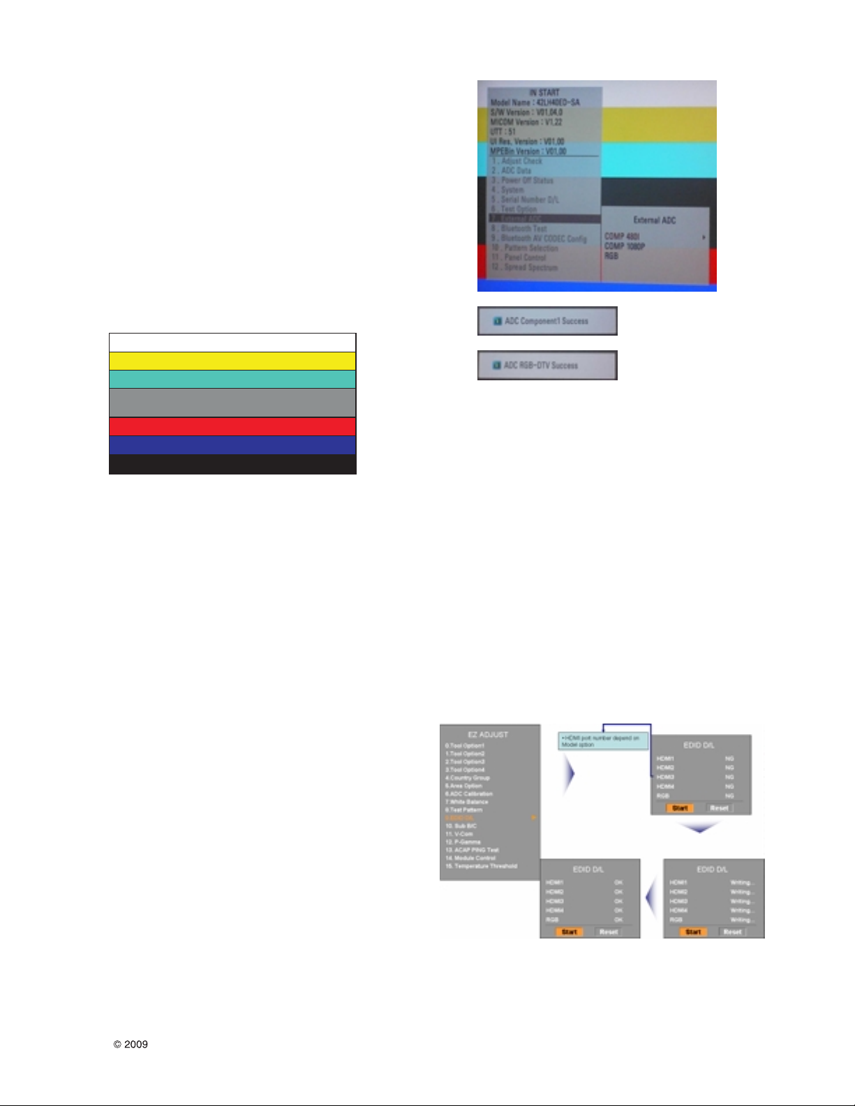
3. Adjustment Items
3.1 PCB Assembly adjustment
• CPLD DOWNLOAD
• Adjust 480i Comp1
• Adjust 1080p Comp1/RGB
- If it is necessary, it can adjustment at Manufacture Line
- You can see set adjustment status at “1. ADJUST
CHECK” of the “In-start menu”
3.2 Set Assembly Adjustment
• EDID (The Extended Display Identification Data ) / DDC
(Display Data Channel) download
• Color Temperature (White Balance) Adjustment
• Make sure RS-232C control
• Selection Factory output option
4. PCB Assembly Adjustment
4.1. CPLD DOWNLOAD : JTAG MODE
4.2. << PRINT PORT >> PIN MAP
Pin JTAG Mode Signal Name
2 TCK
3 TMS
8 TDI
11 TDO
13 15 VCC
18 TO 25 GND
- 11 -
LGE Internal Use OnlyCopyright LG Electronics. Inc. All right reserved.
Only for training and service purposes
4.3. << 10P WAFER >> PIN MAP
- 12 -
LGE Internal Use OnlyCopyright LG Electronics. Inc. All right reserved.
Only for training and service purposes
4.4. Using RS-232C
Adjust 3 items at 3.1 PCB assembly adjustments “4.1.3
sequence” one after the order.
O Adjustment protocol
See ADC Adjustment RS232C Protocol_Ver1.0
O Adjustment protocol
- Pattern Generator : (MSPG-925FA)
- Adjust 480i Comp1 (MSPG-925FA : model :209 , pattern
: 65)
- Adjust 1080p Comp1/RGB(MSPG-925FA:model : 225 ,
pattern : 65)
- Adjust RGB (MSPG-925FA:model :225 , Pattern :65) –
RGB-PC Mode
* If you want more information then see the below Adjustment
method (Factory Adjustment)
O Adjustment sequence
- ad 00 00 : Enter the ADC Adjustment mode.
- xb 00 40: Change the mode to Component1 (No actions)
- ad 00 10: Adjust 480i Comp
- ad 00 10: Adjust 1080p Comp
- xb 00 60: Change to RGB-PC mode(No action)
- ad 00 10: Adjust 1080p RGB
- ad 00 90: End of the adjustment
Order
Command
Set response
1. Inter the ad 00 00 d 00 OK00x
Adjustment mode
2. Change the kb 00 40
b 00 OK40x (Adjust 480i Comp1/1080p Comp1)
Source kb 00 60
b 00 OK60x (Adjust 1080p RGB)
3.
Start Adjustment
ad 00 10
4.Return the OKx ( Success condition )
Response NGx ( Failed condition )
5.Read (main)
(main : component1 480i, RGB 1080p)
Adjustment data
ad 00 20
000000000000000000000000007c007b006dx
(main) (main : component1 1080p)
ad 00 30
000000070000000000000000007c00830077x
6.Confirm ad 00 99 NG 03 00x (Failed condition)
Adjustment NG 03 01x (Failed condition)
NG 03 02x (Failed condition)
OK 03 03x (Success condition)
7.
End of Adjustment
ad 00 90 d 00 OK90x
LGE Internal Use OnlyCopyright LG Electronics. Inc. All right reserved.
Only for training and service purposes
- 13 -
5. Factory Adjustment
5.1 Manual Adjust Component 480i/1080p
RGB 1080p
O Summary : Adjustment component 480i/1080i and RGB
1080p is Gain and Black levelsetting at Analog
to Digital converter, and compensate the RGB
deviation
O Using instrument
- Adjustment remocon, 801GF(802B, 802F, 802R) or
MSPG925FA pattern generator (It can output 480i/1080i
horizontal 100% color bar pattern signal, and its output
level must setting 0.7V±0.1V p-p correctly)
<Pic.4 Adjustment pattern : 480i / 1080p 60Hz Pattern >
* You must make it sure its resolution and pattern cause every
instrument can have different setting
O Adjustment method 480i Comp1, Adjust 1080p
Comp1/RGB (Factory adjustment)
• ADC 480i Component1 adjustment
- Check connection of Component1
- MSPG-925FA Ë Model: 209, Pattern 65
• Set Component 480i mode and 100% Horizontal Color
Bar Pattern(HozTV31Bar), then set TV set to
Component1 mode and its screen to “NORMAL”
• ADC 1080p Component1 / RGB adjustment
- Check connection both of Component1 and RGB
- MSPG-925FA Model: 225, Pattern 65
• Set Component 1080p mode and 100% Horizontal Color
Bar Pattern(HozTV31Bar), then set TV set to
Component1 mode and its screen to “NORMAL”
• After get each the signal, wait more a second and enter
the “IN-START” with press IN-START key of Service
remocon. After then select “7. External ADC” with
navigator button and press “Enter”.
• After Then Press key of Service remocon “Right
Arrow(VOL+)”
• You can see “ADC Component1 Success”
• Component1 1080p, RGB 1080p Adjust is same
method.
• Component 1080p Adjustment in Component1 input
mode
• RGB 1080p adjustment in RGB input mode
• If you success RGB 1080p Adjust. You can see “ADC
RGB-DTV Success”
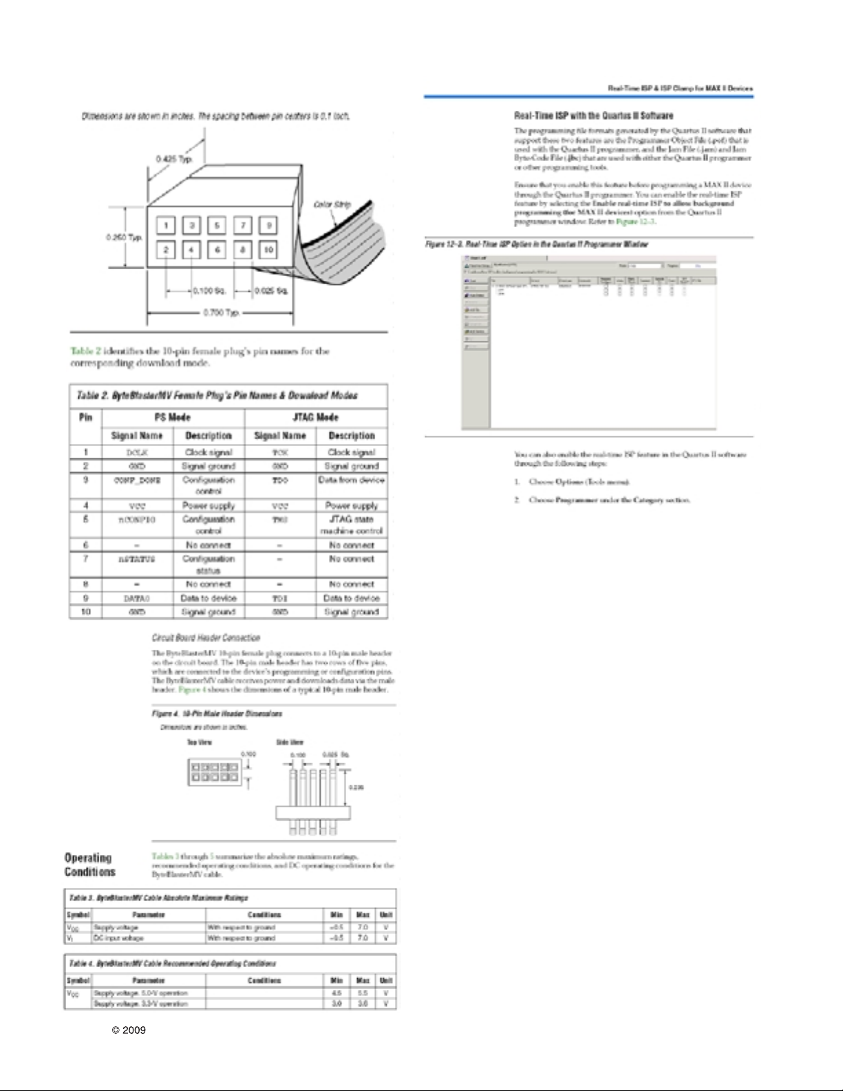
5.2 EDID (The Extended Display
Identification Data) / DDC (Display Data
Channel) Download.
O Summary
• It is established in VESA, for communication between
PC and Monitor without order from user for building user
condition. It helps to make easily use realize “Plug and
Play” function.
• For EDID data write, we use DDC2B protocol.
O Auto Download
• After enter Service Mode by pushing “ADJ” key,
• Enter EDID D/L mode.
• Enter “START” by pushing “OK” key.
Caution: - Never connect HDMI & D-sub Cable when the user
downloading .
- Use the proper cables below for EDID Writing.
- 14 -
LGE Internal Use OnlyCopyright LG Electronics. Inc. All right reserved.
Only for training and service purposes
O Manual Download
• Write HDMI EDID data
- Using instruments
=> Jig. (PC Serial to D-Sub connection) for PC, DDC
adjustment.
=> S/W for DDC recording (EDID data write and
read)
=> D-sub jack
=> Additional HDMI cable connection Jig.
- Preparing and setting.
=> Set instruments and Jig. Like pic.5), then turn on
PC and Jig.
=> Operate DDC write S/W (EDID write & read)
=> It will operate in the DOS mode.
Pic.3) For write EDID data, setting Jig and another instruments.
• EDID data for LJ91D Chassis (Model name = LG TV)
- HDMI-1 EDID table (0x33, 0x2C)
- HDM2 EDID table (0x33, 0x1C)
- HDMI-3 EDID table (0x33, 0x0C)
- Analog (RGB) EDID table (0x9B, 0x25)
PC
Download jig
RGB cable
Main
B/D
Edid data and Model option download (RS232)
NO Item CMD 1 CMD 2 Data 0
Enter
download MODE
Download
Mode In
A E 0 0
When transfer the ’Mode In’ ,
Carry the command.
Edid data and
Model option
download
Download
A E *Note1 *Note2
Automatically download
(The use of a internal Data)
Adjust Mode Out
A E 9 0
Adjustment
Confirmation
A E 9 9
To check Download
on Assembly line.
5.3 Adjustment Color Temperature(White
balance)
O Using Instruments
• Color Analyzer: CA-210 (CH 9)
- Using LCD color temperature, Color Analyzer (CA-210)
must use CH 9, which Matrix compensated (White, Red,
Green, Blue compensation) with CS-2100. See the
Coordination bellowed one.
• Auto-adjustment Equipment (It needs when Autoadjustment – It is availed communicate with RS-232C :
Baud rate: 115200)
• Video Signal Generator MSPG-925F 720p, 216Gray
(Model: 217, Pattern 78)
O Connection Diagram (Auto Adjustment)
• Using Inner Pattern
• Using HDMI input
<Pic.5 Connection Diagram for Adjustment White balance> .
O White Balance Adjustment
If you can’t adjust with inner pattern, then you can adjust
it using HDMI pattern. You can select option at "Ez-Adjust
Menu – 7. White Balance" there items "NONE, INNER,
HDMI". It is normally setting at inner basically. If you can’t
adjust using inner pattern you can select HDMI item, and
you can adjust.
In manual Adjust case, if you press ADJ button of service
remocon, and enter "Ez-Adjust Menu – 7. White
Balance", then automatically inner pattern operates. (In
case of "Inner" originally "Inner" will be selected.
• Connect all cables and equipments like Pic.5)
• Set Baud Rate of RS-232C to 115200. It may set
115200 orignally.
• Connect RS-232C cable to set
• Connect HDMI cable to set
¢ RS-232C Command (Commonly apply)
wb 00 00 White Balance adjustment start.
wb 00 10 Start of adjust gain (Inner white
pattern)
wb 00 1f End of gain adjust
wb 00 20 Start of offset adjust(Inner white
pattern)
wb 00 2f End of offset adjust
wb 00 ff End of White Balance adjust(Inner
pattern disappeared)
• "wb 00 00": Start Auto-adjustment of white balance.
• "wb 00 10": Start Gain Adjustment (Inner pattern)
• "jb 00 c0" :
• …
• "wb 00 1f": End of Adjustment
* If it needs, offset adjustment (wb 00 20-start, wb 00
2f-end)
• "wb 00 ff": End of white balance adjustment (inner
pattern disappear)
- 15 -
LGE Internal Use OnlyCopyright LG Electronics. Inc. All right reserved.
Only for training and service purposes
CA-100+
COL OR
ANALYZER
TYPE; CA-100+
Full W hite Pattern
RS-232C
- 16 -
LGE Internal Use OnlyCopyright LG Electronics. Inc. All right reserved.
Only for training and service purposes
O White Balance Adjustment (Manual adjustment)
• Test Equipment: CA-210
- Using LCD color temperature, Color Analyzer (CA-
210) must use CH 9, which Matrix compensated
(White, Red, Green, Blue compensation) with CS-
2100. See the Coordination bellowed one.
• Manual adjustment sequence is like bellowed one.
- Turn to "Ez-Adjust" mode with press ADJ button of
service remocon.
- Select "10.Test Pattern" with CH+/- button and press
enter. Then set will go on Heat-run mode. Over 30
minutes set let on Heat-run mode.
- Let CA-210 to zero calibration and must has gap more
10cm from center of LCD module when adjustment.
- Press "ADJ" button of service remocon and select
"7.White-Balance" in "Ez-Adjust" then press "▶"
button of navigation key.
(When press "▶" button then set will go to full white
mode)
- Adjust at three mode (Cool, Medium, Warm)
- If "cool" mode
Let B-Gain to 192 and R, G, B-Cut to 64 and then
control R, G gain adjustment High Light adjustment.
- If "Medium" and "Warm" mode
Let R-Gain to 192 and R, G, B-Cut to 64 and then
control G, B gain adjustment High Light adjustment.
- All of the three mode
Let R-Gain to 192 and R, G, B-Cut to 64 and then
control G, B gain adjustment High Light adjustment.
- With volume button (+/-) you can adjust.
- After all adjustment finished, with Enter (■ key) turn
to Ez-Adjust mode. Then with ADJ button, exit from
adjustment mode
Attachment: White Balance adjustment coordination and color
temperature.
O Using CS-1000 Equipment.
- COOL : T=11000K, △uv=0.000, x=0.276 y=0.283
- MEDIUM : T=9300K, △uv=0.000, x=0.285 y=0.293
- WARM : T=6500K, △uv=0.000, x=0.313 y=0.329
5.4 EYE-Q Function check.
1) Turn on TV
2) Press EYE Key of Adj R/C
3) Cover the Eye Q II sensor on the front of the using your
hand and wait for 6 seconds
4) Confirm that R/G/B va;ie os ;pwer tjam 10 of the ‘Raw
Data (Sensor data, Back light)”. If after 6 seconds, R/G/B
value is not lower than 10, re[;ace EYE Q II sensor.
5) Remove your hand from the EYE Q II sensor and wait for
6 sencond
6) Confirm that “OK” pop up.
If change is not seen, replace EYE Q II sensor
5.5 Test of RS-232C control
Press IN-Start button of service remocon then set the “4.Baud
rate” to 15200, Then check RS-232C control and
5.6 Selection of Country option.
Selection of country option is allowed only North American model
(Not allowed Korean model). It is selection of Country about
Rating and Time Zone.
• Models: All models which use LA75A Chassis (See the first
page.)
• Press “In-Start” button of Service Remocon, then enter the
“Option” Menu with “PIP CH-“ Button
• Select one of these three (USA, CANADA, MEXICO)
defends on its market using “Vol. +/-“button.
* Caution : Don’t push The Instop Key ater completing the
function inspection.
6. GND and ESD Testing
6.1 Prepare GND and ESD Testing.
• Check the connection between set and power cord
6.2 Operate GND and ESD auto-test.
• Fully connected (Between set and power cord) set enter
the Auto-test sequence.
• Connect D-Jack AV jack test equipment.
• Turn on Auto-controller(GWS103-4)
• Start Auto GND test.
• If its result is NG, then notice with buzzer.
• If its result is OK, then automatically it turns to ESD Test.
• Operate ESD test
• If its result is NG, then notice with buzzer.
• If its result is OK, then process next steps. Notice it with
Good lamp and STOPER Down.
6.3 Check Items.
• Test Voltage
- GND: 1.5KV/min at 100mA
- Signal: 3KV/min at 100mA
• Test time: just 1 second.
• Test point
- GND test: Test between Power cord GND and Signal
cable metal GND.
- ESD test: Test between Power cord GND and Live and
neutral.
• Leakage current: Set to 0.5mA(rms)
Block Diagram
Overall Block Diagram
for Brazil DTV (LH70)
TU_SCLK, TU_SDATA, TU_SYNC
VA1G5BF8005
RF_Switch, Gain_Switch
TU_CVBS_IN
TU_SIF
SDA0/SCL0_3.3V
LVDS
DDR2(256Mbit)
Qimonda/Hynix
FRC IC
(MST7323S)
LCD Module
(FHD, 120Hz)
JACK BACK
JACK BACK
at REAR
at REAR
AV1
AV2
Component 1
Component 2
D-sub RGB
Audio L/R (for RGB)
HDMI 1
HDMI 2
HDMI 3
Digital Audio (Optic)
RS-232C (Ctrl./SVC)
Bluetooth Module
USB
CVBS, L/R, AV_DET
SIDE_CVBS, SIDE_L/R, SIDE_DET
Y Pb Pr, L/R, DET
Y Pb Pr, L/R, DET
RGB/H/V
Audio L/R
3x1
HDMI Switch
SPDIF
RX/TX RX/TX
MAX3232
DP1/DM1
DP2/DM2
O.C. Protector
+5V+5V
USB_DM1
USB_DP1
USB_DM2
USB_DP2
BCM3556
BCM3556
(Brazil)
(Brazil)
DDR_Data[0:15], DQS, DM …
Addr.[0:13], ctrl. data
Data[16:31]
Data [0 … 7]
CS ,RE,WE……
I2S
SCL, SDA_3.3V
FRC Block
FRC Block
X-tal
12MHz
DDR2 (1Gbit)
DDR2 (1Gbit)
NAND Flash
(512Mbit)
Digital AMP
NTP3100L
NVRAM
Elpida/Hynix
Elpida/Hynix
Reset Switch
Copyright ⓒ 2009 LG Electronics. Inc. All right reserved.
Only for training and service purposes
Reset IC
X-tal
54MHz
SCL, SDA_3.3V
CLK,TDI,TDO,MS,RST
MICOM
(MTV416GMF)
JTAG
X-tal
24MHz
LGE Internal Use Only

Block Diagram
I2C & RS232 Communication
I2C & RS232 Communication
VA1G5BF8005
MAX3232
Sub B/D
47PF
RS232C_RxD
RS232C_TxD
22 ohm
22 ohm
47PF
+5V_ST
4.7k ohm
4.7k ohm
D3.3V
4.7k ohm
4.7k ohm
P
7
0
22 ohm
22 ohm
Main B/D
SCL0
SDA0
SCL1
SDA1
22 ohm
22 ohm
D3.3V
4.7k ohm
4.7k ohm
+3.3V_HDMI
2.7k ohm
2.7k ohm
0 ohm
0 ohm
HDMI
S/W
1
100 ohm
100 ohm
NTP3100L
33PF
D3.3V
BCM3556
SCL3
P
7
0
100 ohm
100 ohm
SDA3
2
22 ohm
22 ohm
4.7k ohm
D3.3V
4.7k ohm
22 ohm
22 ohm
33PF
MICOM
Copyright ⓒ 2009 LG Electronics. Inc. All right reserved.
Only for training and service purposes
SCL2
SDA2
22 ohm
22 ohm
4.7k ohm
4.7k ohm
100 ohm
100 ohm
MST7323
LGE Internal Use Only
Block Diagram
• I2C channel [LH70]
CH0
CH1
BCM3556
BCM3556
CH2
CH3
TUNER 1
TUNER 1
0xC2
0xC2
Demod(0x30)
Demod(0x30)
QPSK(0x32)
QPSK(0x32)
AMP
AMP
NTP3100L
NTP3100L
0x54
0x54
EEPROM
EEPROM
AT24C512
AT24C512
0xA6
0xA6
FRC
FRC
MST7323
MST7323
HDMI SW
HDMI SW
TDA9996
TDA9996
Micom
Micom
MTV416
MTV416
0x50
0x50
CH0 (+3.3V)
(+ 3.3V)
CH1
CH2 (+3.3V)
(+3.3V)
CH3
Copyright ⓒ 2009 LG Electronics. Inc. All right reserved.
Only for training and service purposes
LGE Internal Use Only
Block Diagram
Jack
Jack
Board
Board
D1.2V, D2.5V, +3.3V, +5.0V_ST
SPDIF , EDID_WP ….
SCL0_3.3V, SDA0_3.3V, DDC_SCL, DDC_SDA
CVBS, SIF, AV, RGB ,COMPONENT, R/L,
TU_SCLK, TU_DATA, TU_SYNK’’..
MAIN
MAIN
Board
Board
Copyright ⓒ 2009 LG Electronics. Inc. All right reserved.
Only for training and service purposes
< Signal Interface >
LGE Internal Use Only

1. Power-Up Boot Fail Trouble Shooting
Overall Block Diagram
for Brazil DTV (LH70)
VA1G5BF8005
TU_SCLK, TU_SDATA, TU_SYNC
SDA0/SCL0_3.3V
RF_Switch, Gain_Switch
TU_CVBS_IN
TU_SIF
LVDS
DDR2(256Mbit)
Qimonda/Hynix
FRC IC
(MST7323S)
LCD Module
(FHD, 120Hz)
JACK BACK
JACK BACK
at REAR
at REAR
AV1
AV2
Component 1
Component 2
D-sub RGB
Audio L/R (for RGB)
HDMI 1
HDMI 2
HDMI 3
Digital Audio (Optic)
RS-232C (Ctrl./SVC)
Bluetooth Module
USB
CVBS, L/R, AV_DET
SIDE_CVBS, SIDE_L/R, SIDE_DET
Y Pb Pr, L/R, DET
Y Pb Pr, L/R, DET
RGB/H/V
Audio L/R
3x1
HDMI Switch
SPDIF
RX/TX RX/TX
MAX3232
DP1/DM1
DP2/DM2
O.C. Protector
+5V+5V
USB_DM1
USB_DP1
USB_DM2
USB_DP2
BCM3556
BCM3556
(Brazil)
(Brazil)
DDR_Data[0:15], DQS, DM …
Addr.[0:13], ctrl. data
Data[16:31]
Data [0 … 7]
CS ,RE,WE……
I2S
SCL, SDA_3.3V
FRC Block
FRC Block
X-tal
12MHz
DDR2 (1Gbit)
DDR2 (1Gbit)
NAND Flash
(512Mbit)
Digital AMP
NTP3100L
NVRAM
Elpida/Hynix
Elpida/Hynix
Reset Switch
Copyright ⓒ 2009 LG Electronics. Inc. All right reserved.
Only for training and service purposes
Reset IC
X-tal
54MHz
SCL, SDA_3.3V
CLK,TDI,TDO,MS,RST
MICOM
(MTV416GMF)
JTAG
X-tal
24MHz
LGE Internal Use Only
1. Power-Up Boot Fail Trouble Shooting
Check P801 All Voltage Level
(24V, 12V, 5V_ST)
Y
Check All Voltage Level
at L805/L807/L808
Y
Check Voltage Level 3.3V at L830
Y
Check Voltage Level 2.5V at L827
Y
Check Voltage Level 1.8V
at IC802 #2 pin or L815
Y
Check Voltage Level 1.2V at L821
Y
Check X903 Clock 54MHz
NY
N
N
N
N
N
N
Check Power connector
Replace one of L805/L807/L808
& Recheck
Replace one of
IC809/Q812/L828/L829/L830/L822
& Recheck
Replace one of IC803/L824/L827
& Recheck
Replace one of IC802/IC805/L815
& Recheck
Replace one of
IC804/Q809/L811/L817/L821
& Recheck
Replace X903
N
N
N
N
Replace Power board
Check Micom IC406
Redownload or replace
Y
Check signal transition
at IC101 #9 pin
Y
Replace IC101 Flash Memory
N
Maybe BCM3556 has troubles
Copyright ⓒ 2009 LG Electronics. Inc. All right reserved.
Only for training and service purposes
LGE Internal Use Only
 Loading...