

Page 1
Leica TCS SMD Series
Single Molecule Detection Platform
Technical Documentation
Page 2

General Specifications of SMD Prepared Leica TCS SP5
Microscopes
Microscope anti-vibration table
Z-drive
Continuous wave lasers
Upright
Inverted
Specifi cation For imaging
Vibration insulation Passive
SuperZ galvanometer stage 1500 m travel range/3 nm stepsize
Motorfocus (stand)
Laser type For imaging
VIS
UV Diode, 50 mW: 405 nm
Laser type For imaging
IR
Leica DM6000 CS
Leica DM6000 CFS
Leica DMI6000 CS
Leica DMI6000 CS bottom port
Travel range depending on mechanics
of microscope/15 nm step size
Diode, 40 mW
Ar, 65 mW: 458, 476, 488, 496, 514 nm
HeNe, 1 mW: 543 nm
HeNe, 2 mW: 594 nm
HeNe, 10 mW: 633 nm
DPSS, 20 mW: 561 nm
iSa 1.2 ps 1 W 690...1040 nm
T
(various ranges)
: 442 nm
Pulsed lasers
Excitation modulation
VIS
UV –
Modulation type For imaging
AOTF VIS Up to 8 channels
AOTF UV
EOM IR Yes
Pulsed laser driver Optional
Up to 3 channels
–
–
2
Page 3

Additional SMD Specific Specifications
TCS SMD FCS TCS SMD FLIM TCS SMD FLCS
Yes Yes Yes
Yes Yes Yes
Yes, recommended Yes Yes, recommended
Yes Yes Yes
For FCS For FLIM For FCS and FLIM
Passive Passive Passive
1500 m travel range/3 nm stepsize
Travel range depending on mechanics
of microscope/15 nm step size
For FCS No cw laser excitation for FLIM For FCS
Diode, 40 mW: 442 nm – Diode, 40 mW: 442 nm
Ar
, 65 mW: 458, 476, 488, 496, 514 nm – Ar, 65 mW: 458, 476, 488, 496, 514 nm
HeNe, 1 mW: 543 nm – HeNe, 1 mW: 543 nm
HeNe, 2 mW: 594 nm – HeNe, 2 mW: 594 nm
HeNe, 10 mW: 633 nm – HeNe, 10 mW: 633 nm
DPSS, 20 mW: 561 nm – DPSS, 20 mW: 561 nm
–––
Pulsed excitation for FCS not required For FLIM For FLIM and FLCS
–
–
–
–
1500 m travel range/3 nm stepsize 1500 m travel range/3 nm stepsize
Travel range depending on mechanics
of microscope/15 nm step size
iSa 1.2 ps 1 W 680 ... 1040 nm
T
(various ranges)
Diode, up to 3 mW average @ 40 MHz,
470 nm (software controlled selection of pulse
frequency: 5, 10, 20, 40 MHz), < 90 ps ... < 500 ps
(depending on selected power level)
Diode, up to 4.5 mW average @ 40 MHz,
640 nm (software controlled selection of pulse
frequency: 5, 10, 20, 40 MHz), < 90 ps ... < 400 ps
(depending on selected power level)
Diode, up to 3 mW average @ 40 MHz,
405 nm (software controlled selection of pulse
frequency: 5, 10, 20, 40 MHz), < 70 ps ... < 300 ps
(depending on selected power level)
Travel range depending on mechanics
of microscope/15 nm step size
TiSa 1.2ps 1 W 680 ... 1040 nm
(various ranges)
Diode, up to 3 mW average @ 40 MHz,
470 nm (software controlled selection of pulse
frequency: 5, 10, 20, 40 MHz), < 90 ps ... < 500 ps
(depending on selected power level)
Diode, up to 4.5 mW average @ 40 MHz,
640 nm (software controlled selection of pulse
frequency: 5, 10, 20, 40 MHz), < 90 ps ... < 400 ps
(depending on selected power level)
Diode, up to 3 mW average @ 40 MHz,
405 nm (software controlled selection of pulse
frequency: 5, 10, 20, 40 MHz), < 70 ps ... < 300 ps
(depending on selected power level)
For FCS For FLIM For FCS and FLIM
Up to 8 channels – For FCS: 8 channels
–––
–
– For VIS and UV FLIM: up to 3 channels For VIS and UV FLIM: up to 3 channels
Optional for MP FLIM Optional for MP FLIM
3
Page 4

General Specifications of SMD Prepared Leica TCS SP5
Features For imaging
Number of laser ports Up to 3 (UV - VIS - IR)
Optics
Scanner
Number of lasers
Excitation – emission splitting
Detection range 400...800 nm
UV and IR imaging Sequential or simultaneous
Field upgradable To IR: yes
UV correction
Pinhole Alignment stable single pinhole
Pinhole diameter control
Scanner design For imaging
Scanning concept Optically correct scanning at low inertia
Switch conventional – resonant scanner
Conventional scanner For imaging (PMT and APD)
Maximal line frequency 2800 Hz
Minimal line frequency
Scan speed granulation 1400
Maximal frame rate 512 x 512 5 Hz
Maximal frame rate 512 x 16 50 Hz
Beam park Yes
Maximal frame resolution 8192 x 8192 pixel
Scan zoom 1.0 ... 64 x
Panning Yes
Field rotation 200° optical
Field diameter 22 mm
Up to 8
Acousto Optical Beam Splitter (AOBS
or dichroic beam splitters
Individual precise correction optics
(up to 6 positions)
Motorized by software,
automatic mode available
Conventional and resonant scanner
in one system (optional)
1 Hz
®
)
4
Page 5

Additional SMD Specific Specifications
TCS SMD FCS TCS SMD FLIM TCS SMD FLCS
For FCS For FLIM For FCS and FLIM
1 (VIS) 2 (UV & IR, or UV & VIS)
Up to 8
AOBS For pulsed lasers: dichroic mirrors
Depending on fi lter cube used
––
To FCS: yes To FLIM: yes –
UV not required for FCS Required for UV FLIM To FLCS: yes
Alignment stable single pinhole Alignment stable single pinhole Required for UV FLIM
Motorized by software,
automatic mode available
For FCS For FLIM For FCS and FLIM
Beam park Optically correct scanning at low inertia
Conventional scanner required
Up to 3
Internal SP FLIM: 400 … 800 nm
External FLIM: Depending on fi lter cube used
Motorized by software,
automatic mode available
Conventional and resonant scanner in one
system (optional)
For FCS: 1 (VIS)
For FLIM: 2 (UV & IR, or UV & VIS)
For FCS: up 8,
For FLIM: up to 3
For FCS: AOBS,
For pulsed lasers: dichroic mirrors
Depending on fi lter cube used
Internal SP FLIM: 400 … 800 nm
External FLIM, FCS, and FLCS: Depending on
fi lter cube used
Alignment stable single pinhole
FCS: Beam park
FLIM: optically correct scanning at low inertia
Conventional scanner required, resonant
scanner optional
No scanning during FCS measurement For FLIM data acquisition For FLIM data acquisition
– 1400 Hz 1400 Hz
–
– 1400 1400
– 5 Hz 5 Hz
– 50 Hz 50 Hz
– Yes Yes
– 512 x 512 pixel 512 x 512 pixel
– 1.0 ... 64 x 1.0 ... 64 x
–no no
– 200° optical 200° optical
– 22 mm 22 mm
1 Hz 1 Hz
5
Page 6

General Specifications of SMD Prepared Leica TCS SP5
Resonant scanner For imaging
Maximal line frequency 16000 Hz
Scanner
Scan modes
Minimal line frequency
Scan speed granulation 1
Maximal frame rate 512 x 512 28 Hz
Maximal frame rate 512 x 16 290 Hz
Beam park No
Maximal frame resolution 1024 x 1024 pixel
Scan zoom 1.7 ... 64 x
Panning Yes
Field rotation 200° optical
Field diameter 15 mm
Scan options For imaging
xt Yes
xy Y
xyt Yes
xyλ
xz Yes
xzλ
xyz Yes
xyzλ
xyt Yes
xzt Yes
xyzt Yes
xytz Yes
8000 Hz
es
Yes
Yes
Yes
Beam park positioning
6
Automated brightness control of FLIM images –
Maximum number of FLIM images –
Beam park options For spot bleach (in general software)
xy Yes
xyz
xz No
xzy No
Maximum number of FCS/FLCS measurements –
Maximum number of distinct
measurement points
Maximum number of measurement
repetitions at a point
Maximum number of measurement cycles –
No
–
–
Page 7

Additional SMD Specific Specifications
TCS SMD FCS TCS SMD FLIM TCS SMD FLCS
No scanning during FCS measurement For FLIM data acquisition For FLIM data acquisition
– 8000 Hz 8000 Hz
–
–1 1
– 28 Hz 28 Hz
– 290 Hz 290 Hz
– No No
– 512 x 512 pixel 512 x 512 pixel
– 1.7 ... 64 x 1.7 ... 64 x
–No No
– 200° optical 200° optical
– 15 mm 15 mm
No scanning during FCS measurement For FLIM data acquisition For FLIM data acquisition
–No No
–
– Yes Yes
– Yes (SP FLIM) Yes (SP FLIM)
– Yes Yes
– Yes (SP FLIM) Yes (SP FLIM)
– Yes Yes
– Yes (SP FLIM) Yes (SP FLIM)
– Yes Yes
– Yes Yes
– Yes Yes
–No No
8000 Hz 8000 Hz
Yes Yes
– Yes Yes
– 1000 1000
For automated FCS, FCCS, FLCS data
acquisition series (in FCS wizard)
Yes Yes Yes
s No Yes
Ye
Yes No Ye s
Yes No Ye s
1000 – 1000
100 – 100
100 – 100
100 – 100
For single point lifetime measurement
(in general software)
For automated FCS, FCCS, FLCS data
acquisition series (in FCS wizard)
7
Page 8

General Specifications of SMD Prepared Leica TCS SP5
Detection features Up to 5 PMT for confocal imaging
Emission separation Highly sensitive prism spectral detector
5
2
APDs from PE (SPCM-AQRH series)
or MPD (PDM series)
PE APD: wavelength dependent,
typ. 65% @ 670 nm
MPD APD: wavelength dependent,
typ. 45% @ 550 nm
PE APD: < 250 cps
MPD APD: < 250 cps
Internal confocal detection
External confocal detection
Maximum number of confocal channels
Tunability of emission bands Yes
Spectral detection range 400 – 800 nm
Tuning steps of emission bands 1 nm
Minimal detection range 5 nm
Sensors High sensitivity low noise PMT: R 9624
Dark current –
TTS FWHM –
Detection features 2 APDs for confocal imaging
Emission separation User-exchangeable beam splitting fi lter cubes
Confocal channels
Sensors
Quantum effi ciency
Dark counts
Non-confocal detection
Electronics
Jitter FWHM Not relevant
Dead time Not relevant
Detection types For Imaging
Transmitted light detector Optional, allowing BF, DIC, Ph etc.
Non descanned transmitted light channels Up to 4 channels (MP)
Non descanned refl
Devices
Scanner control Digitally at high performance
Trigger in/out functions Yes
Auxiliary data input channels Up to 2
Max channels in parallel 12
Computer High performance PC workstation
Integration of third party software –
ected light channels Up to 4 channels (MP)
For imaging
eld programmable gate arrays)
(FPGA, fi
–
Programmable control panel with
LCD function & value display
8
Page 9

Additional SMD Specific Specifications
TCS SMD FCS TCS SMD FLIM TCS SMD FLCS
Not for FCS data acquisition Up to 2 FLIM-PMTs for spectral FLIM Up to 2 FLIM-PMTs for spectral FLIM
– Highly sensitive prism spectral detector Highly sensitive prism spectral detector
–
– Yes Yes
– 400 – 800 nm 400 – 800 nm
– 1 nm 1 nm
– 5 nm 5 nm
–
– < 300 cps @ 15 °C < 300 cps @ 15 °C
–
2 external detectors for FCS & FCCS 2 external detectors for FLIM 2 external detectors for
User-exchangeable beam splitting fi lter cubes User-exchangeable beam splitting fi lter cubes User-exchangeable beam splitting fi lter cubes
222
APDs from PE (SPCM-AQRH series)
or MPD (PDM series)
PE APD: wavelength dependent,
typ. 65% @ 670 nm
MPD APD: wavelength dependent,
typ. 45% @ 550 nm
PE APD: < 250 cps
MPD APD: < 250 cps
Not relevant
Below typical count rate (40 ... 70 ns) Below typical count rate (40 ... 70 ns) Below typical count rate (40 ... 70 ns)
None for FCS None for FLIM None for FLIM and FCS
–––
–––
–––
For FCS For FLIM For FCS and FLIM
Digitally at high performance
(FPGA, fi
eld programmable gate arrays)
Not required Required Required
Used for APD imaging Optional: Used for APD imaging Used for APD imaging
12 12 15
Second workstation for FCS
data acquisition and analysis
Client server network connection between work-
stations for full system control and data transfer
2 for FLIM + 3 for imaging 2 for FLIM + 3 for imaging
SP FLIM PMT (Hamamatsu R7400U series,
active cooled)
MP FLIM: < 300 ps
UV & VIS FLIM: < 400 ps
APDs from MPD (PDM series)
Wavelength dependent, typ. 45% @ 550 nm Wavelength dependent, typ. 45% @ 550 nm
MPD APD: < 250 cps MPD APD: < 250 cps
MPD APD:
400 – 500 nm: typ. 200 ps
> 500 nm: down to 50 ps
Digitally at high performance
(FPGA, fi eld programmable gate arrays)
Second workstation for FLIM
data acquisition and analysis
Client server network connection between workstations for full system control and data transfer
SP FLIM PMT (Hamamatsu R7400U series,
active cooled)
MP FLIM: < 300 ps
UV & VIS FLIM: < 400 ps
FCS, FCCS, FLCS, and FLIM
APDs from MPD (PDM series)
MPD APD:
400 – 500 nm: typ. 200 ps
> 500 nm: down to 50 ps
Digitally at high performance
(FPGA, fi eld programmable gate arrays)
Second workstation for FCS and FLIM
data acquisition and analysis
Client server network connection between workstations for full system control and data transfer
Required Required Required
9
Page 10

General Specifications of SMD Prepared Leica TCS SP5
Devices For imaging
Fast ROI-spectrometer Optional
Extensions
Software (LAS AF)
Software options (LAS AF)
Auxiliary emission port
Environment accessories Various options
General Intuitive and guiding user interface
Context sensitive online help system Included
Multi-dimensional data acquisition
Region of interest (ROI) scan Included
Excitation line/frame sequential scan Included
Emission spectrum recording Included
Quantifi cation tools Included
Multi-color restoration, spectral unmixing Included
General time lapse experiment control
tile scanning (mosaic scan)
Dedicated application wizards For imaging
Live Data Mode
Advanced Mark & Find
3D visualization
Colocalization
Deconvolution
MicroLab
Optional
Included
Included
Interactive data recording also allowing
job sequencing and online evaluation
Combines Mark & Find with sophisticated 3D
recordings, Live Data Mode etc.
Maximum and other projections, simulated
fl
uorescence process, rotation animations,
stereo pairs, red-green anaglyphs, height color
coded extended depth of focus images etc.
Histogram based colocalization
and area measurements
Deconvolution option for widefi eld
and confocal images
FRAP wizard, FRAPxt wizard, FLIP wizard,
FRET SE wizard, FRET AB wizard etc.
SMD FCS wizard –
SMD FLIM wizard –
10
Page 11

Additional SMD Specific Specifications
TCS SMD FCS TCS SMD FLIM TCS SMD FLCS
For FCS For FLIM For FCS and FLIM
Not possible Optional with internal SP FLIM
Not possible with external FLIM
Not possible
Various options Various options various options Various options
Included Included Included
Included Included Included
Included
included included included
Included Included Included
Included Included Included
Included Included Included
Included Included Included
Included Included Included
For FCS/FCCS For FLIM For FCS/FCCS/FLCS and for FLIM
Optional with internal SP FLIM
Not possible with external FLIM
Included Included
Not possible
Not possible
–––
–––
–––
–––
–––
–––
FCS wizard for optimization and automation
of FCS and FCCS measurement series
–
–
FLIM wizard for optimization and
automation of FLIM measurement stacks
and time series
FCS wizard for optimization and automation
of FCS, FCCS and FLCS measurement series
FLIM wizard for optimization and
automation of FLIM measurement stacks
and time series
11
Page 12

General Specifications of SMD Prepared Leica TCS SP5
General For imaging
Supported time-resolved analysis methods –
Software features SymphoTime
One-line visualization for time-resolved data
acquisition
FLIM/FCS options For imaging
Data acquisition method –
TCSPC channel width
Resolvable lifetime range –
FLIM analysis For imaging
Data processing –
Fitting models
Optimization methods –
Error test/assessment –
Error analysis –
FCS analysis For imaging
Correlation method –
–
–
–
Fitting model
Optimization methods –
Error test/assessment –
Error analysis –
12
–
Page 13

Additional SMD Specific Specifications
TCS SMD FCS TCS SMD FLIM TCS SMD FLCS
For FCS/FCCS For FLIM For FCS/FCCS/FLCS and for FLIM
FCS, FCCS, FRET, Scripting language
for user
-defi ned analysis routines
Auto- or Crosscorrelation,
Intensity time-trace
For FCS/FCCS For FLIM For FCS/FCCS/FLCS and for FLIM
Time-Tagging of photon arrival times using
T
ime-Correlated Single Photon Counting
(TCSPC) electronics
– min. 4 ps min. 4 ps
–
For FCS/FCCS For FLIM For FCS/FCCS/FLCS and for FLIM
– Whole image or ROIs (arbitrary shape) Whole image or ROIs (arbitrary shape)
–
–
–
– Asymptotic standard errors Asymptotic standard errors
For FCS/FCCS For FLIM For FCS/FCCS/FLCS and for FLIM
Software correlation
(auto- and crosscorrelation)
Pure diffusion, triplet-state, conformational,
protonation, 2D/3D Gaussian PSF
Least squares, Marquardt-Levenberg,
Monto Carlo
Chi-Square, distribution weighted
residuals
Asymptotic standard errors, bootstrap
and support plane analysis
FLIM, FLIM-FRET, Lifetime Histogram,
Scripting language for user-defi ned analysis
routines
FLIM image, Intensity-time trace,
TCSPC histogram
Time-Correlated Single Photon Counting
(TCSPC)
< 100 ps to some µs (depending on system
confi guration and experimental conditions)
1 to 4 exponentials, iterative
reconvolution or tail fi
Least squares, MLE,
Marquardt-Levenberg, Monto Carlo
Chi-Square, distribution weighted
residuals
tting
–
–
–
–
–
FLIM, FLIM-FRET,FCS, FCCS, FLCS, FRET, Lifetime Histogram, Fluorescence Time/Lifetime
Traces, Scripting language for user-defi ned
analysis routines
Auto- or Crosscorrelation, FLIM image,
Intensity-time trace, TCSPC histogram
Time-Correlated Single Photon Counting
(TCSPC)
< 100 ps to some µs (depending on system
confi guration and experimental conditions)
1 to 4 exponentials, iterative
reconvolution or tail fi tting
Least squares, MLE,
Marquardt-Levenberg, Monto Carlo
Chi-Square, distribution weighted
residuals
Software correlation
(auto- and crosscorrelation)
Pure diffusion, triplet-state, conformational,
protonation, 2D/3D Gaussian PSF
Least squares, Marquardt-Levenberg,
Monto Carlo
Chi-Square, distribution weighted
residuals
Asymptotic standard errors, bootstrap
and support plane analysis
13
Page 14

Installation Requirements
VIS Max. 320 kg
Weight base system
Heat load max.
Separate cooling IR laser IR laser, air-cooled heat exchanger (chiller)
Electric supply
Environment
IR Optical bench 900 x 1500 mm: + ca. 280 kg
IR laser system: + ca. 100 kg
SMD specifi c components + up to 160 kg
VIS 3.2 kW
IR 6.2 kW
VIS lasers
( with or without 405 nm cw laser)
IR laser +1x 100 … 120 or 200 … 240 V AC, 15 … 10 A, 50/60 Hz
Chiller for IR laser +1x 100 … 120 or 200 … 240 V AC, 10 A/6 A, 50/60 Hz
SMD +1x 100 … 120 or 200 … 240 V AC, 20 A/16 A, 50/60 Hz
Room temperature +18 to + 25°C, avoid proximity to air conditioning equipment!
Temperature for optimal optical behavior +21 to + 23 °C
Vibration velocity
@ Frequency range 5 Hz–30 Hz
@ Frequency range 5 Hz–30 Hz
Pollution degree Class 2, protect from dust!
Relative humidity 20 – 80% (not condensing)
Illumination Room darkening recommended!
Load carrying capacity 200 kg/m
Door width > 1.00 m
3 x 100 … 120 or 200 … 240 V AC. 1600 VA, 50/60 Hz
< 30 µm/s (effective value)
< 60 µm/s (effective value)
2
visible and ultraviolet radiation:
14
infrared radiation:
Page 15

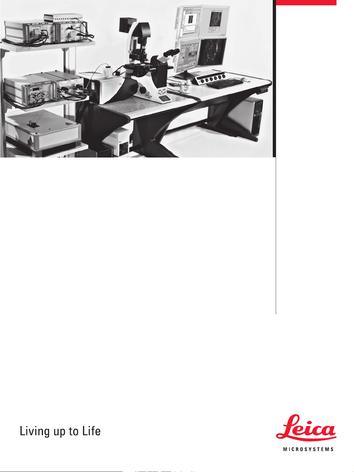
Leica TCS SMD at Inverse Microscope
Leica TCS SMD at Upright Microscope
15
Page 16

“With the user, for the user”
Leica Microsystems
Leica Microsystems operates globally in four divi sions,
where we rank with the market leaders.
Life Science Division
•
The Leica Microsystems Life Science Division supports the
imaging needs of the scientifi c community with advanced
innovation and technical expertise for the visualization,
measurement, and analysis of microstructures. Our strong
focus on understanding scientifi c applications puts Leica
Microsystems’ customers at the leading edge of science.
Industry Division
•
The Leica Microsystems Industry Division’s focus is to
support customers’ pursuit of the highest quality end result.
Leica Microsystems provide the best and most innovative
imaging systems to see, measure, and analyze the microstructures in routine and research industrial applications,
materials science, quality control, forensic science investigation, and educational applications.
Biosystems Division
•
The Leica Microsystems Biosystems Division brings histopathology labs and researchers the highest-quality,
most comprehensive product range. From patient to pathologist, the range includes the ideal product for each
histology step and high-productivity workfl ow solutions
for the entire lab. With complete histology systems featuring innovative automation and Novocastra™ reagents,
Leica Microsystems creates better patient care through
rapid turnaround, diagnostic confi dence, and close customer collaboration.
Surgical Division
•
The Leica Microsystems Surgical Division’s focus is to
partner with and support surgeons and their care of patients with the highest-quality, most innovative surgi cal
microscope technology today and into the future.
The statement by Ernst Leitz in 1907, “with the user, for the user,” describes the fruitful collaboration
with end users and driving force of innovation at Leica Microsystems. We have developed fi ve
brand values to live up to this tradition: Pioneering, High-end Quality, Team Spirit, Dedication to
Science, and Continuous Improvement. For us, living up to these values means: Living up to Life.
Active worldwide
Australia: North Ryde Tel. +61 2 8870 3500 Fax +61 2 9878 1055
Austria: Vienna Tel. +43 1 486 80 50 0 Fax +43 1 486 80 50 30
Belgium: Groot Bijgaarden Tel. +32 2 790 98 50 Fax +32 2 790 98 68
Canada: Richmond Hill/Ontario Tel. +1 905 762 2000 Fax +1 905 762 8937
Denmark: Herlev Tel. +45 4454 0101 Fax +45 4454 0111
France: Rueil-Malmaison Tel. +33 1 47 32 85 85 Fax +33 1 47 32 85 86
Germany: Wetzlar Tel. +49 64 41 29 40 00 Fax +49 64 41 29 41 55
Italy: Milan Tel. +39 02 574 861 Fax +39 02 574 03392
Japan: Tokyo Tel. +81 3 5421 2800 Fax +81 3 5421 2896
Korea: Seoul Tel. +82 2 514 65 43 Fax +82 2 514 65 48
Netherlands: Rijswijk Tel. +31 70 4132 100 Fax +31 70 4132 109
People’s Rep. of China: Hong Kong Tel. +852 2564 6699 Fax +852 2564 4163
Portugal: Lisbon Tel. +351 21 388 9112 Fax +351 21 385 4668
Singapore Tel. +65 6779 7823 Fax +65 6773 0628
Spain: Barcelona Tel. +34 93 494 95 30 Fax +34 93 494 95 32
Sweden: Kista Tel. +46 8 625 45 45 Fax +46 8 625 45 10
Switzerland: Heerbrugg Tel. +41 71 726 34 34 Fax +41 71 726 34 44
United Kingdom: Milton Keynes Tel. +44 1908 246 246 Fax +44 1908 609 992
USA: Bannockburn/lllinois Tel. +1 847 405 0123 Fax +1 847 405 0164
and representatives in more than 100 countries
LEICA and the Leica Logo are registered trademarks of Leica IR GmbH. VI/09/••/••.H.
www.leica-microsystems.com
 Loading...