

Page 1
COMe Reference Carrier-i Type 10
Document Revision 1.0
If it‟s embedded, it‟s Kontron.
Page 2

www.kontron.com
» Table of Contents «
1 User Information ............................................................................ 1
1.1 About This Document ............................................................................................................... 1
1.2 Copyright Notice ..................................................................................................................... 1
1.3 Trademarks ............................................................................................................................ 1
1.4 Standards .............................................................................................................................. 1
1.5 Warranty ............................................................................................................................... 2
1.6 Technical Support ................................................................................................................... 2
2 Introduction ................................................................................. 3
3 Specification ................................................................................. 4
3.1 Functional Specification ........................................................................................................... 4
3.2 Block Diagram ........................................................................................................................ 5
3.3 Mechanical Specification .......................................................................................................... 6
3.4 Electrical Specification ............................................................................................................. 7
3.5 Environmental Specification ...................................................................................................... 8
3.6 MTBF .................................................................................................................................... 8
4 Connector Layout ........................................................................... 9
4.1 Rear Panel ............................................................................................................................. 9
4.2 Connector Locations .............................................................................................................. 10
4.3 Component overview .............................................................................................................. 12
5 Connectors and Features ................................................................. 14
5.1 Power Supply ....................................................................................................................... 14
5.1.1 VCC ................................................................................................................................... 14
5.1.2 Power and Reset Button ........................................................................................................ 15
5.1.3 LID# and SLEEP# Jumper ....................................................................................................... 16
5.2 COM Express® Connector ........................................................................................................ 17
5.3 Status LEDs .......................................................................................................................... 18
Page 3

www.kontron.com
5.4 Serial ATA ............................................................................................................................ 19
5.5 µSD-CARD / Module GPIO ........................................................................................................ 20
5.6 High Definition Audio ............................................................................................................ 22
5.7 Ethernet .............................................................................................................................. 23
5.8 USB .................................................................................................................................... 24
5.9 Mini PCI express .................................................................................................................... 25
5.10 SIM Card.............................................................................................................................. 26
5.11 Kontron Feature Connector ..................................................................................................... 27
5.12 DVI-D and Displayport ............................................................................................................ 28
5.13 Serial Interface ..................................................................................................................... 29
5.14 CAN .................................................................................................................................... 30
5.15 FAN .................................................................................................................................... 31
5.16 SMART Battery ...................................................................................................................... 32
5.16.1 Introduction ....................................................................................................................... 32
5.16.2 Possible Smart Batteries ........................................................................................................ 32
5.16.3 Smart Battery System Manager................................................................................................ 32
5.16.4 Smart Battery Connector ....................................................................................................... 33
6 Battery Information ....................................................................... 34
7 Module Single Supply and Wide Range................................................ 36
8 Compatibility Matrix ....................................................................... 37
9 Security Advice ............................................................................. 38
10 Document Revision History .............................................................. 39
Page 4

COMe Reference Carrier-i Type 10 / User Information
1
1 User Information
1.1 About This Document
This document provides information about products from Kontron Embedded Modules GmbH and/or its subsidiaries.
No warranty of suitability, purpose, or fitness is implied. While every attempt has been made to ensure that the
information in this document is accurate, the information contained within is supplied “as-is” and is subject to
change without notice.
For the circuits, descriptions and tables indicated, Kontron assumes no responsibility as far as patents or other rights
of third parties are concerned.
1.2 Copyright Notice
Copyright © 2003-2010 Kontron Embedded Modules GmbH
All rights reserved. No part of this document may be reproduced, transmitted, transcribed, stored in a retrieval
system, or translated into any language or computer language, in any form or by any means (electronic, mechanical,
photocopying, recording, or otherwise), without the express written permission of Kontron Embedded Modules
GmbH.
DIMM-PC®, PISA®, ETX®, ETXexpress®, microETXexpress™, X-board®, DIMM-IO® and DIMM-BUS® are trademarks or
registered trademarks of Kontron Embedded Modules GmbH. Kontron is trademark or registered trademark of Kontron
AG.
1.3 Trademarks
The following lists the trademarks of components used in this board.
» IBM, XT, AT, PS/2 and Personal System/2 are trademarks of International Business Machines Corp.
» Microsoft is a registered trademark of Microsoft Corp.
» Intel is a registered trademark of Intel Corp.
» All other products and trademarks mentioned in this manual are trademarks of their respective owners.
1.4 Standards
Kontron Embedded Modules GmbH is certified to ISO 9000 standards.
Page 5

COMe Reference Carrier-i Type 10 / User Information
2
1.5 Warranty
This Kontron Embedded Modules GmbH product is warranted against defects in material and workmanship for the
warranty period from the date of shipment. During the warranty period, Kontron Embedded Modules GmbH will at its
discretion decide to repair or replace defective products.
Within the warranty period, the repair of products is free of charge as long as warranty conditions are observed.
The warranty does not apply to defects resulting from improper or inadequate maintenance or handling by the buyer,
unauthorized modification or misuse, operation outside of the product‟s environmental specifications or improper
installation or maintenance.
Kontron Embedded Modules GmbH will not be responsible for any defects or damages to other products not supplied
by Kontron Embedded Modules GmbH that are caused by a faulty Kontron Embedded Modules GmbH product.
1.6 Technical Support
Technicians and engineers from Kontron Embedded Modules GmbH and/or its subsidiaries are available for technical
support. We are committed to making our product easy to use and will help you use our products in your systems.
Please consult our Web site at http://www.kontron.com/support for the latest product documentation, utilities,
drivers and support contacts. Consult our customer section http://emdcustomersection.kontron.com for the latest
BIOS downloads, Product Change Notifications and additional tools and software. In any case you can always contact
your board supplier for technical support.
Page 6
COMe Reference Carrier-i Type 10 / Introduction
3
Article
Part-No.
Description
TBD
TBD
2 Introduction
The TBD carrier board for Type 10 modules is designed to allow embedded application developers to get up and
running quickly on the COM Express® mini platform, giving them a head start on the total system design. Simply
select a Type 10 TBD CPU module, then Plug & Go. The TBD is an evaluation backplane for COM Express® Computer-onModules following the PICMG COM.0 specification Rev 1.0 or Rev 2.0 with pin-out Type 10.
Ordering Information
Page 7

COMe Reference Carrier-i Type 10 / Specification
4
3 Specification
3.1 Functional Specification
» COM Express® COM.0 Rev 2.0 baseboard compatible to Type 10 pin-out based modules
» Designed for extended temperature
» Single supply industrial or commercial power connector (5.5 – 20V)
» 2 x miniPCIexpress
» SIM Card Slot connected to miniPCIexpress
» 2x SATA
» LVDS (40pin JILI FFC40 connector)
» 1 x DDI (either DVI-D (SIL1364 SDVOtoDVI) or Display Port, depends on module capability)
» 1x Ethernet RJ45
» 4 x USB 2.0/1.1 (2x front panel, 2x pin header)
» 1 x USB Client
» Kontron feature connector
» Front panel connectors (HDD Act., Reset and Power Switch)
» Status LED
» µSD-Card Socket
» GPIO pin header for module GPIO (muliplexed with SD-Card)
» LID and SLEEP support
» Power Control functions (Power Button override, module single supply, power consumption measurements)
» Analo Devices AD1882AJCIZHDAudio Codec
- Front panel audio
- Optical S/PDIF output
- Digital S/PDIF output
» Serial COM port on SER0
» CAN on SER1
» Smart Battery Connector for batteries between 7.2V to 14.4V
Page 8

COMe Reference Carrier-i Type 10 / Specification
5
C
O
N
N
E
C
T
O
R
A
B
SATA#0
(J10)
SATA#1
(J11)
DVI-D
(J19)
Feature
Connector (J12)
USB #0-1
(J15)
Ethernet RJ45
(J9)
FrontPanel
Audio (J25)
LVDS/JILI
(J20)
AD1882 AJCIZ
SIL1364
SDVOtoDVI
SATA
HD Audio
PCIe #0
LVDS
DVI
DDI
SMB
RST/PWR Control/MISC
GB-LAN
GPIO2
USB #4
RTC
Battery (B1)
FAN Control
Status LED
J2
DC IN
(J34, optional J35)
VCC 5.5 – 20V
USB Client #7
(J18)
µSD-Card
(J47)
Optical S/PDIF
(J22)
S/PDIF out
(J23)
USB
FET Switch
GPIO
(J38)
GPIO/SDIO
SDIO
COM
(J13)
CAN
(J33)
RX0/TX0
RX1/TX1
4 pin FAN1 12V
(J37)
MAX
3311
TJA
1040
I2C
J40
LID
J41
SLEEP
LAN LED
SUS_STAT/S3/S4/S5
VCC
SIM Card Slot
(J48)
PCIe #1
HDD ACT
J39
USB #5
WLAN LEDs
miniPCIexpress 0
(J26)
miniPCIexpress 1
(J29)
12V DC/DC
12V
MARS / Power
Smart Battery
(J36)
USB #2-3
(J44)
SMB
switch
Display Port
(J49)
DP
SDVO
Power Connector
for HDD
(J51)
3.2 Block Diagram
Page 9
COMe Reference Carrier-i Type 10 / Specification
6
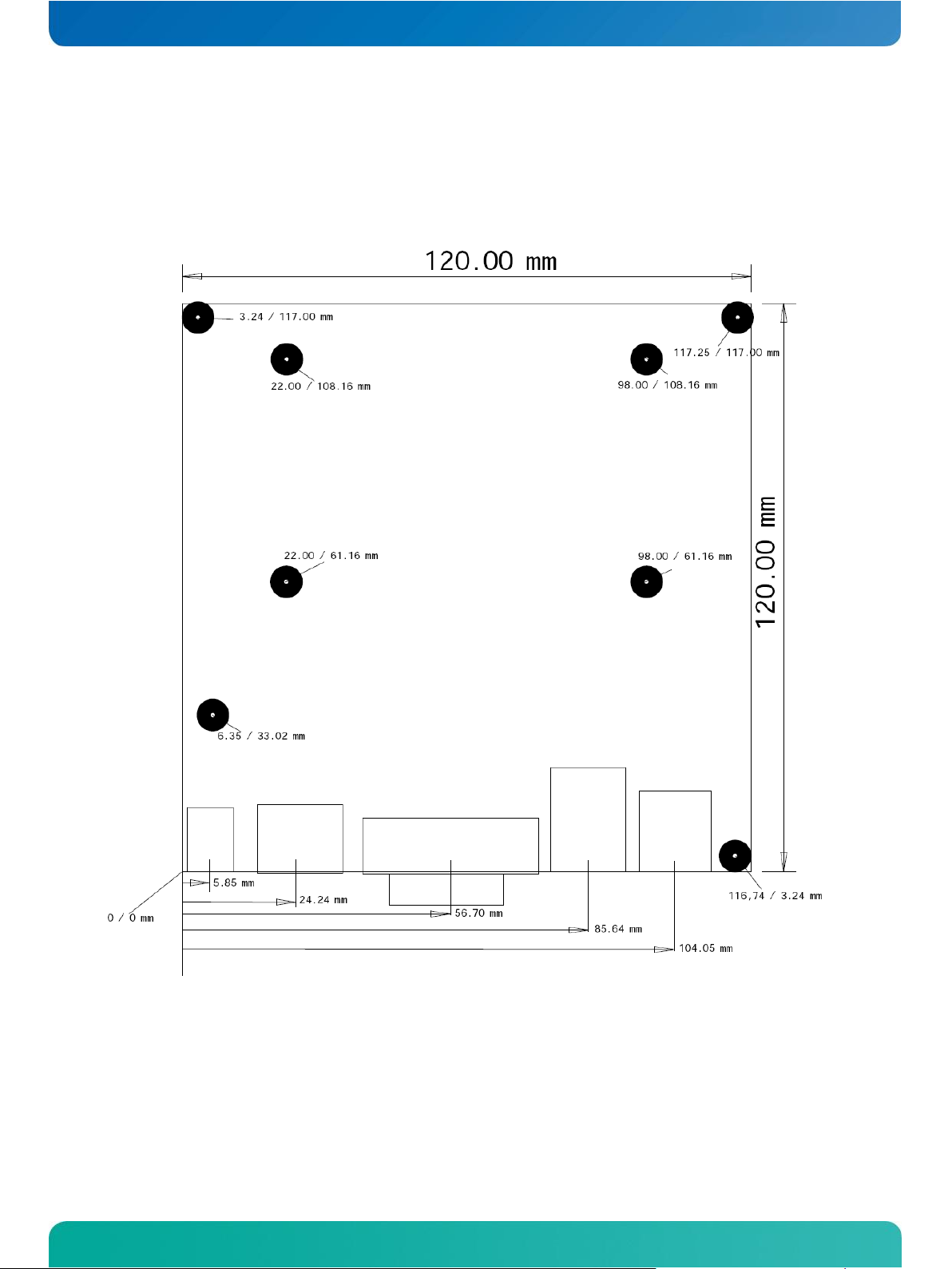
3.3 Mechanical Specification
» Size: 120mm x 120mm
» max height on top: 15.4mm (Connector J15)
Page 10
COMe Reference Carrier-i Type 10 / Specification
7
3.4 Electrical Specification
Supply Voltage
» Single Power Supply (5.5V – 20V DC)
When external devices are supplied by the COMe Reference Carrier-I Type 10 (via HDD power and LVDS connector) and
the temperature is below 0°C the carrier board supply voltage shall be > 6.5V.
Power Supply Rise time
» The input voltages shall rise from ≤10% of nominal to within the regulation ranges within 0.1ms to 20ms.
» There must be a smooth and continuous ramp of each DC input voltage from 10% to 90% of its final set-point
following the ATX specification
Supply Voltage Ripple
» Maximum 100 mV peak to peak 0-20MHz
Power Connector
» Pin / Ring Type with 2,1mm pin diameter
Page 11

COMe Reference Carrier-i Type 10 / Specification
8
1
1
3.5 Environmental Specification
Ambient temperature
» Operating: -40°C to +85 °C
» Non-operating: -40 to +85 °C
Humidity
» Operating: 10% to 90% (non condensing)
» Non operating: 5% to 95% (non condensing)
3.6 MTBF
The following MTBF (Mean Time Between Failures) values were calculated using a combination of manufacturer‟s test
data, if the data was available, and a Bellcore calculation for the remaining parts. The Bellcore calculation used is
“Method 1 Case 1”. In that particular method the components are assumed to be operating at a 50 % stress level in a
40° C ambient environment and the system is assumed to have not been burned in. Manufacturer‟s data has been
used wherever possible. The manufacturer‟s data, when used, is specified at 50° C, so in that sense the following
results are slightly conservative. The MTBF values shown below are for a 40° C in an office or telecommunications
environment. Higher temperatures and other environmental stresses (extreme altitude, vibration, salt water
exposure, etc.) lower MTBF values.
» System MTBF: tbd hours
The whole carrier board was designed to accomplish industrial temperature range. This was not possible for all
connectors and chips. Following devices have a different temperature rating:
» Audio Codec: -20°C to +85°C
» DVI Connector: 0°C to 60°C
Page 12
COMe Reference Carrier-i Type 10 / Connector Layout
9
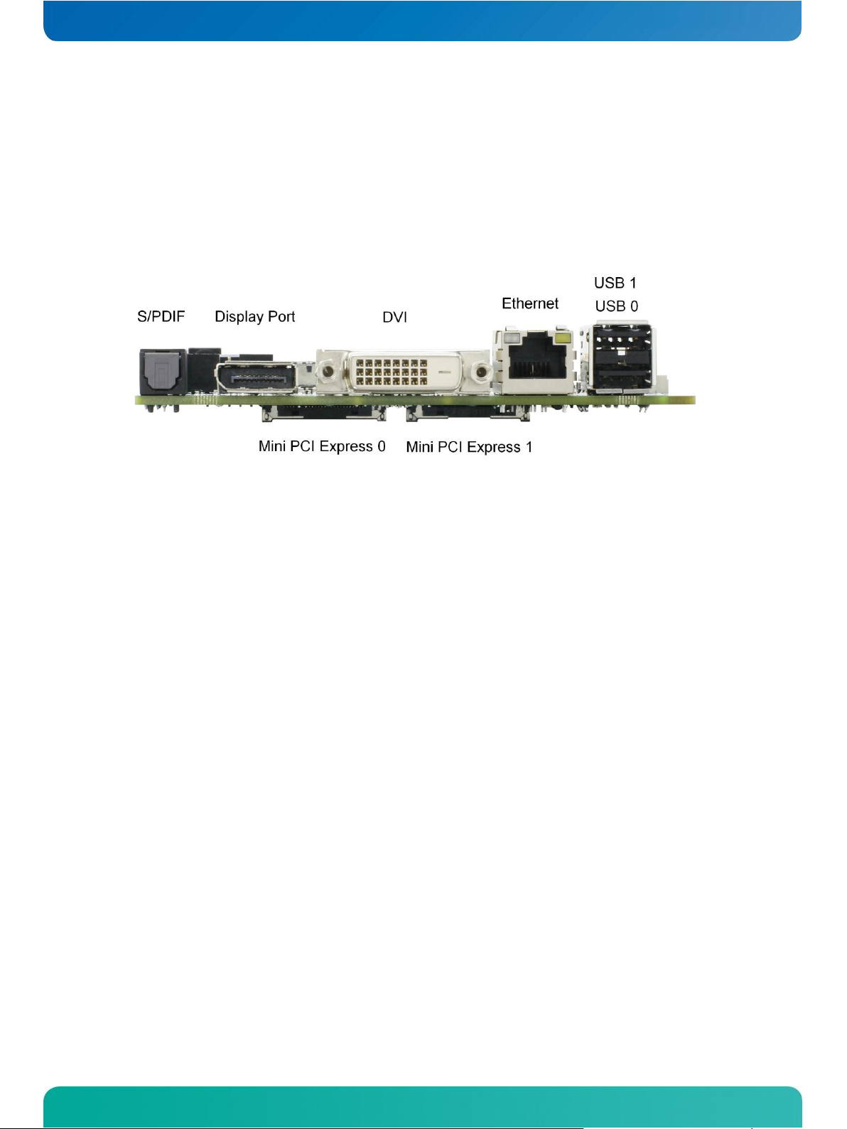
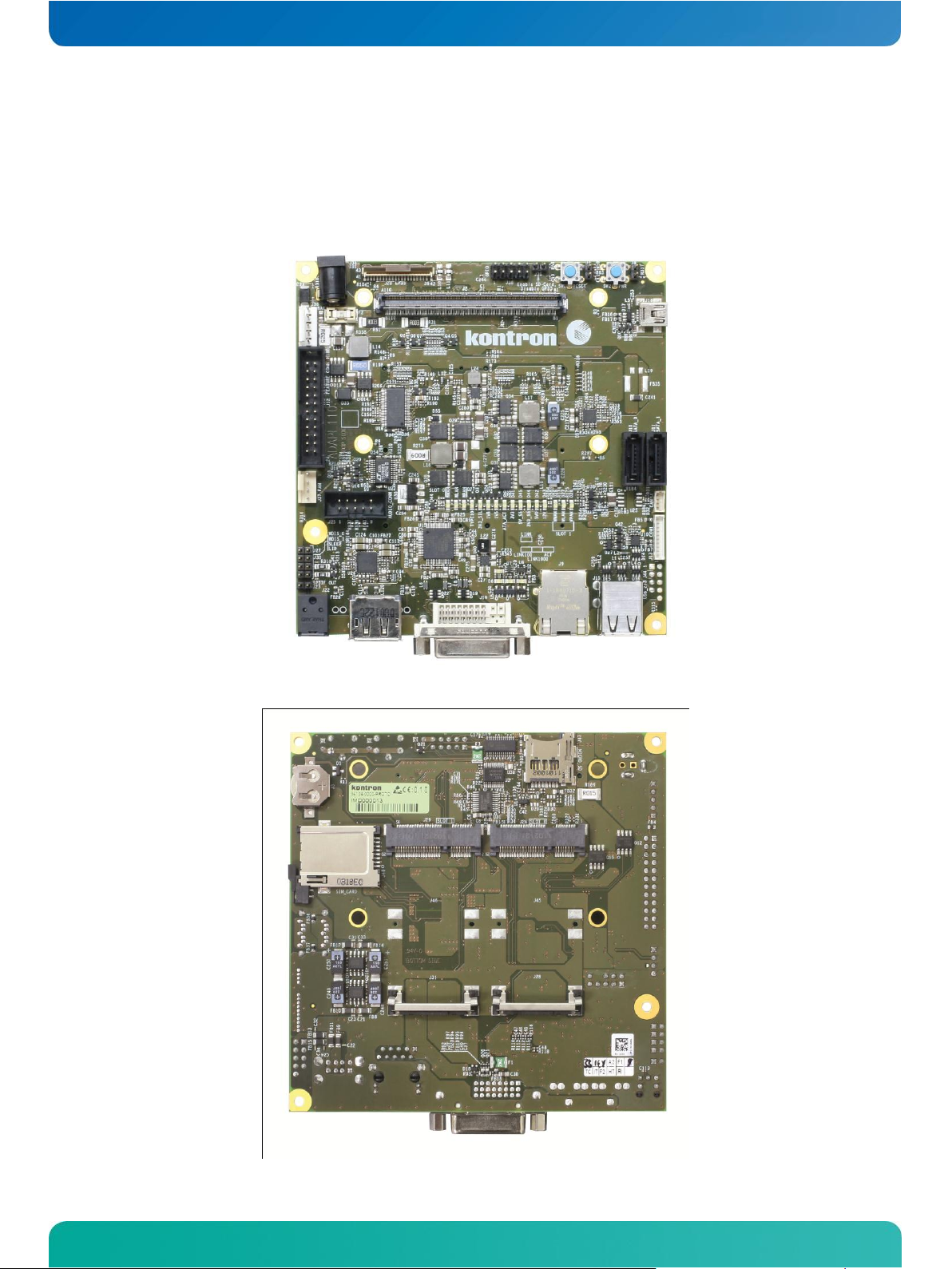
4 Connector Layout
4.1 Rear Panel
Page 13
COMe Reference Carrier-i Type 10 / Connector Layout
10
4.2 Connector Locations
Page 14

COMe Reference Carrier-i Type 10 / Connector Layout
11
Page 15

COMe Reference Carrier-i Type 10 / Connector Layout
12
Connector
Short Description
B01-B04
Baseboard mounting holes
D8
LAN LINK100
D9
LAN LINK1000
D10
LAN LINK
D11
LAN ACT
D12
HDD ACT
D23
Mini PCIe WWAN 0
D24
Mini PCIe WLAN 0
D25
Mini PCIe WPAN 0
D26
Mini PCIe WWAN 1
D27
Mini PCIe WLAN 1
D28
Mini PCIe WPAN 1
D41
V3.3 S0
D42
V5.0 S0
D43
V12_S0
D44
V3.3 S5
D45
V5.0 S5
D46
V1.5 S0
D47
V1.8 S0
D48
V3.3 S0 Sil
F2
Fuse
SW1
Reset Button
SW2
Power Button
J2
COM Express Connector
J3
RTC Battery Socket
J7
Reset Button Jumper
J8
Power Button Jumper
J9
Ethernet RJ45
J10
SATA #0
J11
SATA #1
J12
Feature Connector
J13
Serial COM
J15
USB #0 - #1
J18
USB Client #7
J19
DVI-D
J20
LVDS/JILI
J22
Optical S/PDIF
J23
Digital S/PDIF out
J25
Front Panel Audio
J26
Mini PCI Express 0
J29
Mini PCI Express 1
J32
Display Port/SDVO Jumper
J33
CAN
J34
DCin
J35
DCin (optional)
J36
Smart Battery
J37
Fan Connector
4.3 Component overview
Page 16

COMe Reference Carrier-i Type 10 / Connector Layout
13
J38
GPIO
J39
SDIO/GPIO Jumper
J40
LID Jumper
J41
Sleep Button
J44
Frontpanel USB
J47
µSD-Card
J48
SIM Card
J49
Display Port Connector
J51
Power Connector (for HDD)
J52
S5 Eco Jumper
U3
Reset Buffer
U10
Serial Transciever
U15
SDVO to DVI transmitter
U18
Smart Battery Manager
U19
GPIO/SDIO switch
U25
CAN Transciever
U26
HD Audio Codec
U31
PCIe Clock Buffer
U43
Display Port – SDVO Switch
Page 17

COMe Reference Carrier-i Type 10 / Connectors and Features
14
Connector
Type
Matching Connector
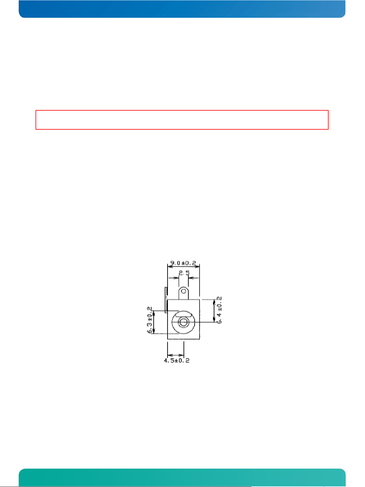
J34
Cliff: DC10A
Cliff: DCPP1
J35 (optional)
Phoenix Contact: MC 1,5/ 2-G-3,5 (1844210)
Phoenix Contact: MC 1,5/ 2-ST-3,5 (1840366)
Connector
Pin
Signal
J34
1 (Pin)
VCC
2 (Shield)
GND
J35
1
VCC
2
GND
5 Connectors and Features
5.1 Power Supply
5.1.1 VCC
The COM Express® Reference Carrier Board‟s power supply is a single supply connection with two possible connectors.
The standard connector is a pin ring type with 2.1mm pin.
Optionally a 3.5mm pitch horizontal PCB header can be equipped.
Page 18

COMe Reference Carrier-i Type 10 / Connectors and Features
15
Connector
J7
Reset Button
SW1
J8
Power Button
SW2
5.1.2 Power and Reset Button
Power and Reset Button is available as switch as well as jumper.
Page 19

COMe Reference Carrier-i Type 10 / Connectors and Features
16
Connector
J40
LID#
J41
SLEEP#
5.1.3 LID# and SLEEP# Jumper
The specifications update for PICMG COM.0 modules to revision 2.0 implements new signals for LID# and SLEEP#. The
low active signals can be simulated by switch 5 and 6 similar to notebook functionality of closing the lid or pressing
the sleep button.
Page 20

COMe Reference Carrier-i Type 10 / Connectors and Features
17
5.2 COM Express® Connector
The COMe Reference Carrier-i Type 10 is a reference backplane for Type 10 based Computer-on-Modules. Both types
are module pin-outs based on one connectors with 2 rows (Row A and B) with 220 pins overall. Please refer to your
module documentation for detailed pin-out descriptions.
Note: The Type 10 pin-out is compatible to Type 2 and Type 6. It's possible to drive Computer-on-Modules based on
pin-out Type 2 and Type 6 on this evaluation baseboard without functionality of second COM Express®
connector CD and 2nd DDI on connector AB.
Page 21

COMe Reference Carrier-i Type 10 / Connectors and Features
18
LED
Description
D8
LAN LINK100
D9
LAN LINK1000
D10
LAN LINK
D11
LAN ACT
D12
HDD ACT
D23
Mini PCIe WWAN 0
D24
Mini PCIe WLAN 0
D25
Mini PCIe WPAN 0
D26
Mini PCIe WWAN 1
D27
Mini PCIe WLAN 1
D28
Mini PCIe WPAN 1
D41
V3.3 S0
D42
V5.0 S0
D43
V12_S0
D44
V3.3 S5
D45
V5.0 S5
D46
V1.5 S0
D47
V1.8 S0
D48
V3.3 S0 for Silicon Image SIL1364
5.3 Status LEDs
Page 22

COMe Reference Carrier-i Type 10 / Connectors and Features
19
SATA Pin
Signal
1
Ground
2
Transmit +
3
Transmit -
4
Ground
5
Receive -
6
Receive +
7
Ground
Connector
SATA Port
J10
SATA #0
J11
SATA #1
5.4 Serial ATA
The COM Express® Type 10 pin-out specification according to COM.0 specification revision 2.0 defines 2 SATA ports.
The COM Express® Type 10 Reference Carrier Board provides two 7-pin SATA data connectors as standard 1.27mm
Pitch Serial ATA High Speed Header with Locking Latch.
Page 23

COMe Reference Carrier-i Type 10 / Connectors and Features
20
PIN
Name
Description
PIN
Name
Description
1
DAT2
Data Line 2
5
CLK
Clock Line
2
DAT3
Data Line 3 / Card Detect
6
GND
Signal Ground
3
CMD
Command/Response
7
DAT0
Data Line 0
4
Vdd
Supply Voltage - 3.3V
8
DAT1
Data Line 1
5.5 µSD-CARD / Module GPIO
The SD-Card standard is a standard for removable memory storages designed and licensed by the SD Card Association
(http://sdcard.org). The card form factor, electrical interface and protocol are all part of the SD Card specification.
COM Express® Type 1 and Type 10 pin-out based modules may provide a SDIO interface shared with GPIO signals.
Therefore on COM Express® Reverence Carrier Type 10 a µSD-Card connector is available. Please check the
documentation of your module if SDIO is supported and how to enable.
Close configuration jumper39 (default) to enable µSD-Card Slot J47 or open J39 to enable GPIO pin-header J38.
µSD Card Pin Description
Page 24

COMe Reference Carrier-i Type 10 / Connectors and Features
21
GPIO J38 PIN
Description
GPIO J38 Pin
Description
1
VCC 3.3V
2
GPO0 / SD_CLK
3
GPI0 / SD_DATA0
4
GPO1 / SD_CMD
5
GPI1 / SD_DATA1
6
GPO2 / SD_WP
7
GPI2 / SD_DATA2
8
GPO3 / SD_CD#
9
GPI3 / SD_DATA3
10
GND
Note: The switching circuitry which selects GPIO or SDIO interface may influence the signal quality of SDIO which
results in detection or boot issues with some fast SD/SDHC cards. Therefore it's recommended to reduce
SDIO interface speed to 24MHz in module's BIOS if supported
Page 25

COMe Reference Carrier-i Type 10 / Connectors and Features
22
Pin
Description
Pin
Description
1
MIC2-L
6
MIC2-JD
2
GND 7 SENSE
3
MIC2-R (MIC Power)
8
Key Pin
4
PRESENCE#
9
Line2-L (LineOut-L)
5
LINE2-R (LineOut-R)
10
LINE2-JD
Pin
J23 (S/PDIF out)
1
SPDIF_OUT
2
GND
5.6 High Definition Audio
The COMe Reference Carrier-i Type 10 provides HDAudio via AD1882AJC High Definition Audio Codec supporting
analog, optical and digital audio connections.
Front Panel Audio Connector J25
The Front Panel Audio Connector J25 on COMe Reference Carrier-i Type 10 allows connecting a chassis front panel adio
with analog microphone input and stereo speaker output.
Digital Audio Output J23
Connector J23 offers a digital S/P-DIF connection.
Optical Audio Output J22
Connector J22 offers a TOSLINK compatible optical S/P-DIF connection.
Page 26

COMe Reference Carrier-i Type 10 / Connectors and Features
23
Function
J9 Left LED
J9 Right LED
Activity
-
Yellow
Link10
- - Link100
Green
-
Link1000
Orange
-
Carrier Board Diodes
Short Description
D8
LAN LINK100
D9
LAN LINK1000
D10
LAN LINK
D11
LAN ACT
5.7 Ethernet
The COMe Reference Carrier-i Type 10 provides a RJ45 connector. Ethernet Connector J9 with integrated magnetics
and LED is configured to support modules with Gigabit Ethernet controller only. Modules with 10/100 MBit Ethernet
controller are not supported.
Page 27

COMe Reference Carrier-i Type 10 / Connectors and Features
24
USB Client connectorJ18 - Pin
J18 Function
1
USB Client Power detect
2
USB7-
3
USB7+
4
n.c. 5 GND
6-9
Shield GND
USB front panel connectorJ44 - Pin
J3 Function
1
USB Power (+5V)
2
USB Power (+5V)
3
USB2-
4
USB3-
5
USB2+
6
USB3+
7
GND
8
GND
10
Shield GND
5.8 USB
The COM Express® module's USB ports 0 to 1 are available on rear panel connector J15. USB ports 2 and 3 are located
on the front panel connector. USB ports 4 and 5 are used on mini PCI express connector.
Additionally USB7 is available on USB mini-A connector J18 as non-powered connector for USB client functionality.
Check the documentation of your module if USB client on Port #7 is supported and J18 can be used.
Page 28

COMe Reference Carrier-i Type 10 / Connectors and Features
25
MiniPCIe J29 / J26 - Pin
Function
MiniPCIe J29 / J26 - Pin
Function
1
WAKE#
2
3,3V
3
Reserved
4
GND
5
Reserved
6
1,5V 7 CLKREQ#
8
UIM_PWR
9
GND
10
UIM_DATA
11
REFCLK-
12
UIM_CLK
13
REFCLK+
14
UIM_RESET
15
GND
16
UIM_VPP
Mechanical Key
17
Reserved
18
GND
19
Reserved
20
Reserved
21
GND
23
PERST#
23
PERn0
24
+3,3Vaux
25
PERp0
26
GND
27
GND
28
+1,5V
29
GND
30
SMB_CLK
31
PETn0
32
SMB_DATA
33
PETp0
34
GND
35
GND
36
USB_D-
37
Reserved
38
USB_D+
39
Reserved
40
GND
41
Reserved
42
LED_WWAN#
43
Reserved
44
LED_WLAN#
45
Reserved
46
LED_WPAN#
47
Reserved
48
+1,5V
49
Reserved
50
GND
51
Reserved
52
+3,3V
5.9 Mini PCI express
The COMe Reference Carrier-i Type 10 provides two full functional miniPCIexpress card sockets, one in full size one in
half size. All signals are equipped: USB, PCIe and the UIM signals are connected to the SIM card socket.
Page 29

COMe Reference Carrier-i Type 10 / Connectors and Features
26
5.10 SIM Card
The COMe Reference Carrier-i Type 10 provides a SIM Card connector to use radio based services on miniPCIexpress
connectors J26 and J29.
Page 30

COMe Reference Carrier-i Type 10 / Connectors and Features
27
Pin
Signal
Level
Signal Description
1
PWR_+5V
5V power
+5V UL-protected with inductor (600R@100MHz, 1A)
2
GPO2
3.3V-O
General-purpose power management event output
3
#BATLOW
3.3V-I
Battery low input. May be driven low by external circuitry to signal that the system battery is low,
or may be used to signal some other external power management event.
4
GPI2
3.3V-I
General-purpose power management event input
5
#SYS_RESET
3.3V-I
This input may be driven low by external circuitry in order to reset the power management logic
6
WDT
3.3V-O
Indicating that a Watchdog Timeout Event has occurred (non buffered module output)
7
LPC_SERIRQ
3.3V-I
Serial interrupt request. This pin is used to support the serial interrupt protocol.
8 - -
Not connected
9
I2C_DAT
3.3V-IO
Data line of I2C-Bus
10
#SMB_ALERT
3.3V-I
System Management Bus Alert input. May be driven low by SMB devices in order to signal an event
on the SM Bus
11
I2C_CLK
3.3V-O
Clock line of I2C-Bus
12
SMB_DAT
3.3V-IO
Clock and data line of SM-Bus.
13
SMB_CLK
3.3V-O
14 - -
Not connected
15
#WAKE1
3.3V-I
Low driven general purpose wake-up signal
16
VCC_RTC
3V-I
3V backup cell input. Should be connected to a 3V backup cell for RTC operation and storage
register non-volatility in the absence of system power. (VBATT = 2.4 – 3.3V)
17
#THRM
3.3V-I
Input from off-module temperature sensor indicating an over temperature situation
18
GND
GND
Ground
19
PWR_OK
3.3V-I
High active input indicating that power from the power supply is ready. It can also be used as low
active reset input signal.
20
GND
GND
Ground
21
#PWRBTN
3.3V-I
Power Button Input. This input is used to support the ACPI Power Button function.
22
GND
GND
Ground
23
#ATA_ACT
3.3V-O
Low active output signal, which indicates activity on IDE interfaces.
24
#CB_RESET
3.3V-O
Low active Reset output from module to carrier board
5.11 Kontron Feature Connector
The Kontron Feature connector provides additional interfaces such as I2C, SMBus or Power Control Signals. See the
table below for detailed pin-out description.
Page 31

COMe Reference Carrier-i Type 10 / Connectors and Features
28
J32 Setting
Usage
Closed
DVI (default)
Open
Displayport
5.12 DVI-D and Displayport
On COMe Reference Carrier-i Type 10 the DVI output is available through a Silicon Image SiL1364/A SDVO to single link
DVI PanelLink Transmitter. Check your module documentation if SDVO is available on DDI interface defined for Type 10
pin-out based modules. If this is not the case, then please switch to Displayport usage with Jumper J32.
Page 32

COMe Reference Carrier-i Type 10 / Connectors and Features
29
Pin
J13 (COMA)
1
n.c.
2
n.c. 3 RX0
4
n.c.
5
TX0 6 n.c.
7
n.c.
8
n.c. 9 GND
10
+5V
5.13 Serial Interface
The PICMG COM.0 specification revision 2.0 defines two optional 2-pin serial interfaces on COM Express® connector
pins A98/A99 and A101/A102 formerly used for 12V VCC input.SER0 can be used as a serial COM port on COMe
Reference Carrier-i Type 10 at connector J13.
J13 allows SER0 as 2-pin RS232 interface COMA with Kontron Adapter cable KAB-DSUB9-2. Please check the
documentation of your module if this interface is supported and how to configure.
Page 33

COMe Reference Carrier-i Type 10 / Connectors and Features
30
Pin
J33 (CAN)
1
GND
2
n.c.
3
CAN_H
4
CAN_L
5.14 CAN
The PICMG COM.0 specification revision 2.0 defines two optional 2-pin serial interfaces on COM Express® connector
pins A98/A99 and A101/A102 formerly used for 12V VCC input. On some modules the 2nd serial interface can be used
as a CAN connection, which is provided by J33.
J33 allows to be used as CAN connector together with Kontron Adapter Cable KAB-CAN-1.
Page 34

COMe Reference Carrier-i Type 10 / Connectors and Features
31
Pin
J37 1 GND
2
+12V
3
Sense
4
Control (PWM)
5.15 FAN
The COMe Reference Carrier-i Type 10 privides one 4-pin PWM FAN connector directly controlled by the module FAN
output specified in the COM.0 revision 2.0 specification if supported by the module.
Page 35

COMe Reference Carrier-i Type 10 / Connectors and Features
32
5.16 SMART Battery
5.16.1 Introduction
The Core of the SBS is the dual Smart Battery System Manager LTC1760. On COMe Reference Carrier-i Type 10 only one
battery connection is provided.
Smart Battery Systems have the ability to communicate with the application. Therefore the user gets information
about the current state of the battery. The interface for this communication is the System Management Bus (SMBus).
Standard Smart Batteries have a specified 5 pin header, connecting to the power lines and additionally this SMBus.
This standardization allows using all available kinds of standard Smart Batteries, which also applies to the COMe
Reference Carrier-i Type 10.
A typical SBS consists of a Smart Battery System Manager and a charger, which can communicate with the chipset
using the SMBus. If there is no software to control the SBS via SM-bus then the system is able to run in a stand alone
mode with reduced functionality, too.
The SBS was designed for the requirements of the COMe Reference Carrier-i Type 10. Additionally different kinds of
Smart Batteries can be used. That means different battery chemistry and cell configurations. But it must be ensured to
use standard Smart Batteries, which meet the SM-Bus standard.
Note: Please ensure that the input voltage of the COMe Reference Carrier-i Type 10 is higher than the charging
voltage of the connected SMART battery. Otherwise the battery can not be charged.
5.16.2 Possible Smart Batteries
The SBS hardware is configured for a maximum charger output voltage of 8,4V and a maximum output current of 2 A.
Smart Batteries with a nominal voltage of 7,2V, e.g. NiMH and NiCd with 6SxP (= 6 cells in series and x in parallel) or
Li-Ion and LiPo with 2SxP (= 2 cells in series and x in parallel) are possible.
Battery Manufacturer:
http://www.moltechpower.co.uk/smart_standard_range.htm
e.g. ND2057, NH2057
http://www.inspired-energy.com/Standard_Products/standard_products.htm
http://www.emergingpower.com/oem/oem_standardpacks.htm
5.16.3 Smart Battery System Manager
The LTC1760 SBS Manager is a highly integrated level 3 battery charger and selector intended for products using dual
smart batteries. Three SMBus interfaces allow the LTC1760 to servo to the internal voltage and currents measured by
the batteries while allowing a SMBus Host to monitor either battery‟s status. Charging accuracy is determined by the
battery‟s internal voltage and current measurement, typically better then ±0,2%.
Page 36

COMe Reference Carrier-i Type 10 / Connectors and Features
33
The LTC1760 automatically switches between power sources in less than 10μs to prevent power interruption upon
battery or wall adapter removal. It implements all elements of a version 1.1 “Smart Battery System Manager” except
for the generation of composite battery information. An internal multiplexer cleanly switches the SMBus Host to the
attached Smart Battery without generating partial messages to the battery or SMBus host. The Thermistor on the
battery is automatically monitored for temperature and disconnection information (SafetySignal).
Hardware programmable limits for maximum charge current and voltage improve the safety of the complete system.
For more information see datasheet of LTC1760.
5.16.4 Smart Battery Connector
Page 37

COMe Reference Carrier-i Type 10 / Battery Information
34
6 Battery Information
The used Battery is a BAT 1225
English:
CAUTION: Danger of explosion if battery is incorrectly replaced. Replace only with the same or equivalent type
recommended by the manufacturer. Dispose of used batteries according to the manufacturer‟s
instructions.
Deutsch:
VORSICHT: Explosionsgefahr bei unsachgemäßem Austausch der Batterie. Ersatz nur durch denselben oder
einen vom Hersteller empfohlenen gleichwertigen Typ. Entsorgung gebrauchter Batterien nach
Angaben des Herstellers.
French:
ATTENTION: Risque d„explosion avec l„échange inadéquat de la batterie. Remplacement seulement par le même
ou un type équivalent recommandé par le producteur. L‟évacuation des batteries usagées
conformément à des indications du fabricant.
Danish:
ADVARSEL: Lithiumbatteri – Eksplosionsfare ved fejlagtig Håndtering. Udskifting må kun ske med batteri af
samme fabrikant og type. Lever det brugte batteri tilbage til leverand
Page 38

COMe Reference Carrier-i Type 10 / Battery Information
35
Finnish:
VAROITUS: Paristo voi rãjãhtãã, jos se on virheellisesti asennettu. Vaihda paristo ainoastaanlaltevalmistajan
suosittelmaan tyyppiln. Havita kaytetty paristo valmistajan ohjeiden mukaisesti.
Spanish:
Precaución: Peligro de explosión si la batería se sustituye incorrectamente. Sustituya solamente por el mismo o
tipo equivalente recomendado por el fabricante. Disponga las baterías usadas según las
instrucciones del fabricante.
Note: The battery of this product is not considered to be accessible by the end user. Therefore the safety
instructions are only given in English, German, French, Danish, Finish and Spanish language.
If the battery of this product however is accessible by the end user, it is in the responsibility of the
Kontron customer to give the corresponding safety instructions in the required language(s).
Page 39

COMe Reference Carrier-i Type 10 / Module Single Supply and Wide Range
36
7 Module Single Supply and Wide Range
The COMe Reference Carrier-i Type 10 is supplied via a single wide range supply between 5.5V and 20V. Please ensure
that also your module supports wide range input of that range.
Please check the documentation of your product if a wide range voltage input is supported. Kontron Computer -onModules usually supports:
» COM Express® modules in ultra size form factor (nanoETXexpress):
4.75V to 14V
» COM Express® modules in compact and basic size form factor (microETXexpress and ETXexpress)
8.5V to 18V
J52 enables Carrier Board‟s S5Eco mode, when open. Default is closed.
Page 40

COMe Reference Carrier-i Type 10 / Compatibility Matrix
37
Con
Feature
nanoETXexpress-SP (Type1)
nanoETXexpress-TT (Type10)
J15
ATX 12V Power
4.75V - 14V
4.75V - 14V
J25
PCIexpress Slot A
if PCIe Switch is disabled
if PCIe Switch is disabled
J26
PCIexpress Slot B
if PCIe Switch is enabled
if PCIe Switch is enabled
J27
PCIexpress Slot C
if PCIe Switch is disabled
if PCIe Switch is disabled
J41
ExpressCard
YES, but USB#5 is USB 2.0 only
YES
J38
PCI Slot0
if PCIe Switch is enabled
YES
J39
PCI Slot 1
if PCIe Switch is enabled
YES
J41
Express Card
if PCIe Switch is enabled
YES
J34
SATA1
on variants without onboard LAN
YES
J61
USB #4 / USB #6
Ethernet RJ45
USB 2.0 only
No USB #6
J44
PWM FAN (SIO/Module)
SIO YES / Modoule NO
SIO YES / Module optional
J68
DVI-D (SDVO2DVI)
Optional
YES
J74
LPC FWH for external BIOS
YES
NO
J76
SPI Flash for external BIOS
NO
YES
J78
RS232 COMA from module
NO
YES
J79
RS232 COMB from module
NO
YES
J83
SER0 from module
NO
YES
J84
SER1 from module
NO
YES
J92
LID
NO
Optional
SW6
SLEEP
NO
Optional
8 Compatibility Matrix
The COM Express® Eval Type 10 supports Computer-on-Modules following PICMG COM.0 Revision 1.0 pin-out Type 1 or
COM.0 revision 2.0 pin-out Type 10.
See table below wich features are supported by Kontron's COM Express® ultra form factor modules 'nanoETXexpress':
Page 41

COMe Reference Carrier-i Type 10 / Security Advice
38
9 Security Advice
To protect the external power lines to peripheral devices the customer has to take care about:
- The wires to the external device have the right diameter to withstand the max. available current
- The housing of the external device fulfils the fire protection requirements of IEC/EN 60950.
Page 42

COMe Reference Carrier-i Type 10 / Document Revision History
39
Revision
Date
Edited by
Changes
0.10_prelim
24.08.11
UMA
Initial Release
0.2
03.11.11
UMA
Added mechanical measures, added functional and connector description.
1.0
07.02.11
UMA
Corrected Ethernet description, added warning for low voltage use
Europe, Middle East & Africa
Oskar-von-Miller-Str. 1
85386 Eching/Munich
Germany
Tel.: +49 (0)8165/ 77 777
Fax: +49 (0)8165/ 77 219
info@kontron.com
North America
14118 Stowe Drive
Poway, CA 92064-7147
USA
Tel.: +1 888 294 4558
Fax: +1 858 677 0898
info@us.kontron.com
Asia Pacific
17 Building,Block #1,ABP.
188 Southern West 4th Ring
Beijing 100070, P.R.China
Tel.: + 86 10 63751188
Fax: + 86 10 83682438
info@kontron.cn
10 Document Revision History
Corporate Offices
 Loading...