

Page 1
COMe-mSP1
Document Revision 160
www.kontron.com
Page 2

Page 3

» Table of Contents «
1 User Information..................................................................................6
1.1 About This Document.................................................................................................................... 6
1.2 Copyright Notice.......................................................................................................................... 6
1.3 Trademarks................................................................................................................................. 6
1.4 Standards................................................................................................................................... 6
1.5 Warranty.................................................................................................................................... 7
1.6 Technical Support......................................................................................................................... 7
2 Introduction........................................................................................8
2.1 Product Description...................................................................................................................... 8
2.2 Naming clarification..................................................................................................................... 8
2.3 Understanding COM Express® Functionality.......................................................................................9
2.4 COM Express® Documentation....................................................................................................... 10
2.5 COM Express® Benefits................................................................................................................ 10
3 Product Specification...........................................................................11
3.1 Modules & Accessories................................................................................................................. 11
3.2 Functional Specification............................................................................................................... 13
3.3 Block Diagram............................................................................................................................ 17
3.4 Electrical Specification................................................................................................................18
3.4.1 Supply Voltage........................................................................................................................... 18
3.4.2 Power Supply Rise Time................................................................................................................ 18
3.4.3 Supply Voltage Ripple.................................................................................................................. 18
3.4.4 Power Consumption..................................................................................................................... 18
3.4.5 ATX Mode.................................................................................................................................. 19
3.4.6 Single Supply Mode..................................................................................................................... 19
3.5 Power Control............................................................................................................................ 20
3.6 Environmental Specification......................................................................................................... 21
3.6.1 Temperature Specification............................................................................................................ 21
3.6.2 Humidity................................................................................................................................... 21
3.7 Standards and Certifications......................................................................................................... 22
3.8 MTBF........................................................................................................................................ 24
3.9 Mechanical Specification.............................................................................................................. 25
3.9.1 Module Dimension...................................................................................................................... 25
3.9.2 Height on Top............................................................................................................................ 25
3.9.3 Height on Bottom....................................................................................................................... 25
3.9.4 Mechanical Drawing.................................................................................................................... 25
3.10 Thermal Management.................................................................................................................. 26
3.11 Heatspreader............................................................................................................................. 26
4 Features and Interfaces.......................................................................27
4.1 Onboard SSD.............................................................................................................................. 27
4.2 LPC.......................................................................................................................................... 28
www.kontron.com
Page 4

COMe-mSP1 /
4.3 LPC boot................................................................................................................................... 29
4.4 M.A.R.S.................................................................................................................................... 30
4.5 Fast I2C & SMBus........................................................................................................................ 31
4.6 JIDA16 and JIDA32..................................................................................................................... 32
4.7 K-Station 1................................................................................................................................ 33
4.8 K-Station & API Resources............................................................................................................ 34
4.8.1 I2C.......................................................................................................................................... 34
4.8.2 Storage.................................................................................................................................... 34
4.8.3 GPIO........................................................................................................................................ 34
4.8.4 Hardware Monitor....................................................................................................................... 34
4.9 GPIO - General Purpose Input and Output.........................................................................................35
4.10 Watchdog Timer.......................................................................................................................... 36
4.11 Flash Backup Feature................................................................................................................... 37
4.12 Speedstep Technology................................................................................................................. 39
4.13 C-States.................................................................................................................................... 40
4.14 Hyper Threading......................................................................................................................... 41
4.15 ACPI Suspend Modes and Resume Events..........................................................................................42
4.16 USB......................................................................................................................................... 43
4.17 SDIO........................................................................................................................................ 44
4.18 Graphics Interface...................................................................................................................... 45
4.19 LPC Bus..................................................................................................................................... 47
5 System Resources...............................................................................49
5.1 Interrupt Request (IRQ) Lines........................................................................................................ 49
5.1.1 In 8259 PIC Mode........................................................................................................................ 49
5.1.2 In APIC mode............................................................................................................................. 50
5.2 Memory Area.............................................................................................................................. 51
5.3 I/O Address Map......................................................................................................................... 51
5.4 Peripheral Component Interconnect (PCI) Devices............................................................................. 52
5.5 Internal I2C Bus......................................................................................................................... 52
5.6 JILI I2C Bus............................................................................................................................... 52
5.7 SDVO I2C Bus............................................................................................................................. 52
5.8 System Management (SM) Bus....................................................................................................... 52
5.9 Pinout List................................................................................................................................ 53
5.9.1 General Signal Description............................................................................................................ 53
5.9.2 Connector X1A Row A................................................................................................................... 54
5.9.3 Connector X1A Row B................................................................................................................... 56
5.9.4 SDVO Connector J1801 (optional)...................................................................................................58
5.9.5 XDP Connector J1400 (optional).................................................................................................... 59
6 BIOS Operation...................................................................................60
6.1 Determining the BIOS Version....................................................................................................... 60
6.2 BIOS Update.............................................................................................................................. 60
6.3 Setup Guide............................................................................................................................... 61
6.3.1 Start AMI® BIOS Setup Utility........................................................................................................61
6.4 BIOS Setup................................................................................................................................ 63
6.4.1 Main Menu................................................................................................................................ 63
6.4.2 Module Info............................................................................................................................... 67
4
Page 5

COMe-mSP1 /
6.4.3 Advanced Menu.......................................................................................................................... 71
6.4.4 Advanced PCI/PnP Settings........................................................................................................... 91
6.4.5 Boot........................................................................................................................................ 91
6.4.6 Security.................................................................................................................................... 94
6.4.7 Advanced Chipset Settings............................................................................................................ 94
6.4.8 Exit Menu.................................................................................................................................. 99
5
Page 6

COMe-mSP1 / User Information
1 User Information
1.1 About This Document
This document provides information about products from Kontron Europe GmbH and/or its subsidiaries. No warranty of
suitability, purpose, or fitness is implied. While every attempt has been made to ensure that the information in this
document is accurate, the information contained within is supplied “as-is” and is subject to change without notice.
For the circuits, descriptions and tables indicated, Kontron assumes no responsibility as far as patents or other rights of
third parties are concerned.
1.2 Copyright Notice
Copyright © 2003-2012 Kontron Europe GmbH
All rights reserved. No part of this document may be reproduced, transmitted, transcribed, stored in a retrieval system, or
translated into any language or computer language, in any form or by any means (electronic, mechanical, photocopying,
recording, or otherwise), without the express written permission of Kontron Europe GmbH.
DIMM-PC®, PISA®, ETX®, ETXexpress®, microETXexpress®, X-board®, DIMM-IO® and DIMM-BUS® are trademarks or
registered trademarks of Kontron Europe GmbH. Kontron is trademark or registered trademark of Kontron AG.
1.3 Trademarks
The following lists the trademarks of components used in this board.
» IBM, XT, AT, PS/2 and Personal System/2 are trademarks of International Business Machines Corp.
» Microsoft is a registered trademark of Microsoft Corp.
» Intel is a registered trademark of Intel Corp.
» All other products and trademarks mentioned in this manual are trademarks of their respective owners.
1.4 Standards
Kontron Europe GmbH is certified to ISO 9000 standards.
6
Page 7

COMe-mSP1 / User Information
1.5 Warranty
This Kontron Europe GmbH product is warranted against defects in material and workmanship for the warranty period
from the date of shipment. During the warranty period, Kontron Europe GmbH will at its discretion decide to repair or
replace defective products.
Within the warranty period, the repair of products is free of charge as long as warranty conditions are observed.
The warranty does not apply to defects resulting from improper or inadequate maintenance or handling by the buyer,
unauthorized modification or misuse, operation outside of the product’s environmental specifications or improper
installation or maintenance.
Kontron Europe GmbH will not be responsible for any defects or damages to other products not supplied by Kontron
Europe GmbH that are caused by a faulty Kontron Europe GmbH product.
1.6 Technical Support
Technicians and engineers from Kontron Europe GmbH and/or its subsidiaries are available for technical support. We are
committed to making our product easy to use and will help you use our products in your systems.
Please consult our Web site at http://www.kontron.com/support for the latest product documentation, utilities, drivers
and support contacts. Consult our customer section http://emdcustomersection.kontron.com for the latest BIOS
downloads, Product Change Notifications, Board Support Packages, DemoImages, 3D drawings and additional tools and
software. In any case you can always contact your board supplier for technical support.
7
Page 8

COMe-mSP1 / Introduction
2 Introduction
2.1 Product Description
This credit card sized COM Express® mini module is compatible to COM Express® pin-out Type 1. On 55 mm x 84 mm
footprint COMe-mSP1 is a perfect fit for the next generation of low power, ultra-mobile applications that require energy
saving x86 processor performance, high-end graphics, PCI Express and Serial ATA combined with longer battery life. These
include handheld devices for medical or multi-media applications, small mobile data systems and a host of new
applications that have not previously been possible due to size or power consumption limitations.
The Kontron COM Express® mini COM, COMe-mSP1, is based on the highly-efficient Intel® Atom™ Z5xx processor series
and Intel® System Controller Hub single chip that combines the memory controller, graphic engine and I/O in a single,
space saving chipset design. With only one tenth of the Thermal Design Power and one seventh the size of ULV processors
at an identical performance, the COMe-mSP1 COM offers an unprecedented power consumption / performance ratio for
x86-based ultra-mobile designs.
The COMe-mSP1 with Flash and memory on-board support 1 PCI Express x1 (opt. 2 x1 if no onboard LAN), Serial ATA, High
Definition Audio, LVDS and optional SDVO. 10/100/1000 Gigabit Ethernet is designed in onboard for high connectivity
and 8x USB provides fast and sufficient interfaces for external peripherals.
All above mentioned requirements are supported by COM Express® mini - small power - low size - high performance.
2.2 Naming clarification
COM Express® defines a Computer-On-Module, or COM, with all components necessary for a bootable host computer,
packaged as a super component.
» COMe-bXX# modules are Kontron's COM Express® modules in basic form factor (125mm x 95mm), formerly known
as ETXexpress®
» COMe-cXX# modules are Kontron's COM Express® modules in compact form factor (95mm x 95mm), formerly known
as microETXexpress®
» COMe-mXX# modules are Kontron's COM Express® modules in mini form factor (55mm x 84mm), formerly known as
nanoETXexpress
The product names for Kontron COM Express® Computer-on-Modules consist of a short form of the industry standard
(COMe-), the form factor (b=basic, c=compact, m=mini), the capital letters for the CPU and Chipset Codenames (XX) and
the pin-out type (#) followed by the CPU Name.
8
Page 9
COMe-mSP1 / Introduction
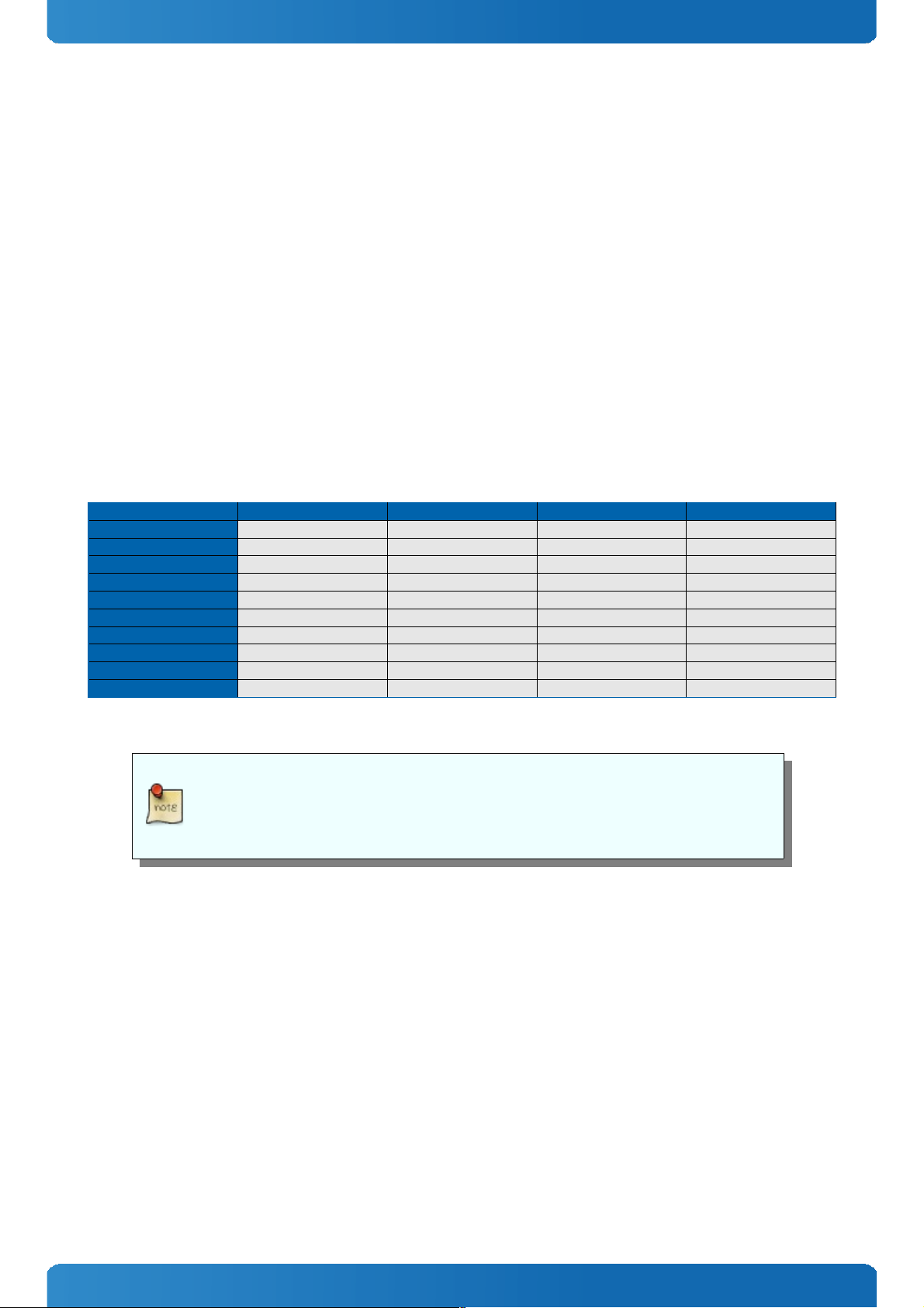
2.3 Understanding COM Express® Functionality
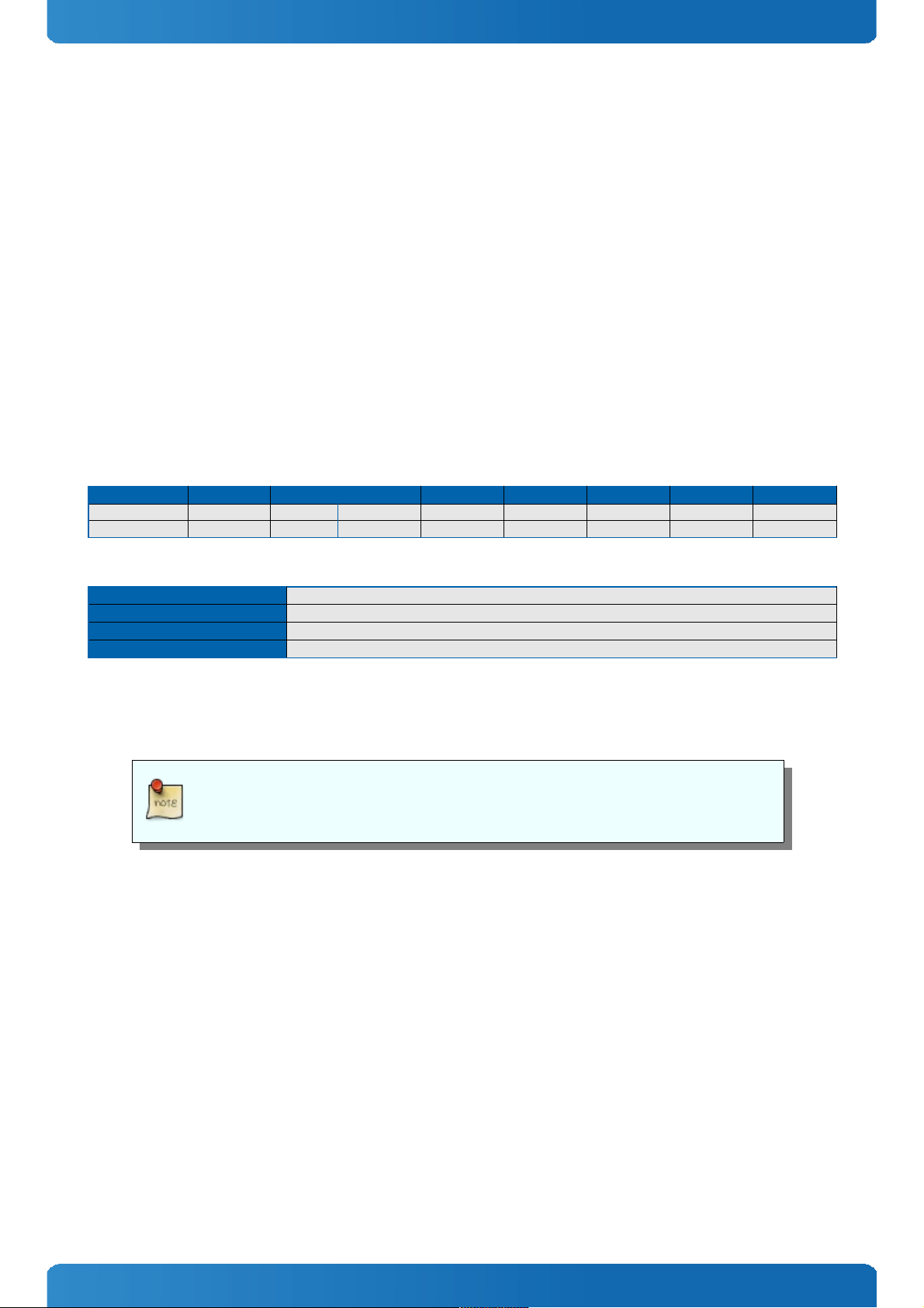
All Kontron COM Express® basic and compact modules contain two 220pin connectors; each of it has two rows called Row
A & B on primary connector and Row C & D on secondary connector. COM Express® Computer-on-modules feature the
following maximum amount of interfaces according to the PICMG module Pin-out type:
Feature Pin-Out Type 1 Pin-Out Type 10 Pin-Out Type 2 Pin-Out Type 6
HD Audio
1x 1x 1x 1x
Gbit Ethernet
1x 1x 1x 1x
Serial ATA
4x 4x 4x 4x
Parallel ATA
- - 1x -
PCI
- - 1x -
PCI Express x1
6x 6x 6x 8x
PCI Express x16 (PEG)
- - 1x 1x
USB Client
1x 1x - -
USB 2.0
8x 8x 8x 8x
USB 3.0
- 2x - 4x
VGA
1x - 1x 1x
LVDS
Dual Channel Single Channel Dual Channel Dual Channel
DP++ (SDVO/DP/HDMI/DVI)
1x optional 1x 3x shared with PEG 3x
LPC
1x 1x 1x 1x
External SMB
1x 1x 1x 1x
External I2C
1x 1x 1x 1x
GPIO
8x 8x 8x 8x
SDIO
1x optional 1x optional - -
UART (2-wire COM)
- 2x - 2x
FAN PWM out
- 1x - 1x
9
Page 10
COMe-mSP1 / Introduction
2.4 COM Express® Documentation
This product manual serves as one of three principal references for a COM Express® design. It documents the
specifications and features of COMe-mSP1. Additional references are are available from your Kontron Support or from
PICMG®:
» The COM Express® Specification defines the COM Express® module form factor, pin-out, and signals. This document
is available from the PIGMG website by filling out the order form.
» The COM Express® Design Guide by PICMG serves as a general guide for baseboard design, with a focus on maximum
flexibility to accommodate a wide range of COM Express® modules.
Some of the information contained within this product manual applies only to certain
product revisions (CE: xxx). If certain information applies to specific product revisions (CE:
xxx) it will be stated. Please check the product revision of your module to see if this
information is applicable.
2.5 COM Express® Benefits
COM Express® modules are very compact, highly integrated computers. All Kontron COM Express® modules feature a
standardized form factor and a standardized connector layout that carry a specified set of signals. Each COM is based on
the COM Express® specification. This standardization allows designers to create a single-system baseboard that can
accept present and future COM Express® modules.
The baseboard designer can optimize exactly how each of these functions implements physically. Designers can place
connectors precisely where needed for the application on a baseboard designed to optimally fit a system’s packaging.
A single baseboard design can use a range of COM Express® modules with different size and pin-out. This flexibility can
differentiate products at various price/performance points, or to design future proof systems that have a built-in upgrade
path. The modularity of a COM Express® solution also ensures against obsolescence as computer technology evolves. A
properly designed COM Express® baseboard can work with several successive generations of COM Express® modules.
A COM Express® baseboard design has many advantages of a custom, computer-board design but delivers better
obsolescence protection, greatly reduced engineering effort, and faster time to market.
10
Page 11
COMe-mSP1 / Product Specification
3 Product Specification
3.1 Modules & Accessories
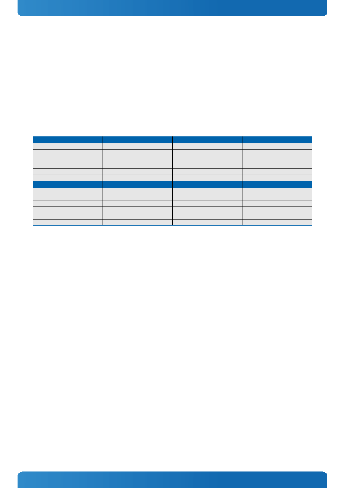
The COM Express® mini sized Computer-on-Module COMe-mSP1 (NOW1) follows pin-out Type 1 and is compatible to PICMG
specification COM.0 Rev 1.0. The COMe-mSP1, based on Intel's eMenlow platform, is available in different variants to
cover the demand of different performance, price and power:
Commercial grade modules (0°C to 60°C operating)
Product Number Product Name Processor SCH and Features
34001-2040-16-1 COMe-mSP1 Z530 2GB/4GB Intel® Atom™ Z530 US15W, 1xPCIe, 2GB DDR2, 4GB SSD
34001-1040-16-1 COMe-mSP1 Z530 1GB/4GB Intel® Atom™ Z530 US15W, 1xPCIe, 1GB DDR2, 4GB SSD
34001-5120-16-1 COMe-mSP1 Z530 512MB/2GB Intel® Atom™ Z530 US15W, 1xPCIe, 512MB DDR2, 2GB SSD
34001-1020-11-1 COMe-mSP1 Z510 1GB/2GB Intel® Atom™ Z510 US15W, 1xPCIe, 1GB DDR2, 2GB SSD
34001-5151-11-1 COMe-mSP1 Z530 512/512MB Intel® Atom™ Z510 US15W, 1xPCIe, 512MB DDR2, 512MB SSD
Extended temperature modules (E1, -25°C to 75°C operating)
Product Number Product Name Processor SCH and Features
34001-1040-16-1EXT COMe-mSP1 Z530 1GB/4GB E1 Intel® Atom™ Z530 US15W, 1xPCIe, LAN, 1GB DDR2, 4GB SSD
34001-5120-16-1EXT COMe-mSP1 Z530 512/2GB E1 Intel® Atom™ Z530 US15W, 1xPCIe, LAN, 512MB DDR2, 2GB SSD
34001-5151-11-1EXT COMe-mSP1 Z510 512/512M E1 Intel® Atom™ Z510 US15W, 1xPCIe, LAN, 512MB DDR2, 512MB SSD
Possible memory and onboard Flash configurations 34001-MMFF-xx-x:
» MM = 51: 512MB DDR2 Memory (4 x 1Gb chips on bottom)
» MM = 10: 1024MB DDR2 Memory (8 x 1Gb chips)
» MM = 20: 2048MB DDR2 Memory (8 x 2Gb chips)
» FF = 00: without PATA SSD
» FF = 51: 512MB onboard PATA SSD
» FF = 10: 1GB onboard PATA SSD
» FF = 20: 2GB onboard PATA SSD
» FF = 40: 4GB onboard PATA SSD
Please contact your local sales for customized Memory and Flash variants or modules with
2xPCIe (no-LAN version)
11
Page 12

COMe-mSP1 / Product Specification
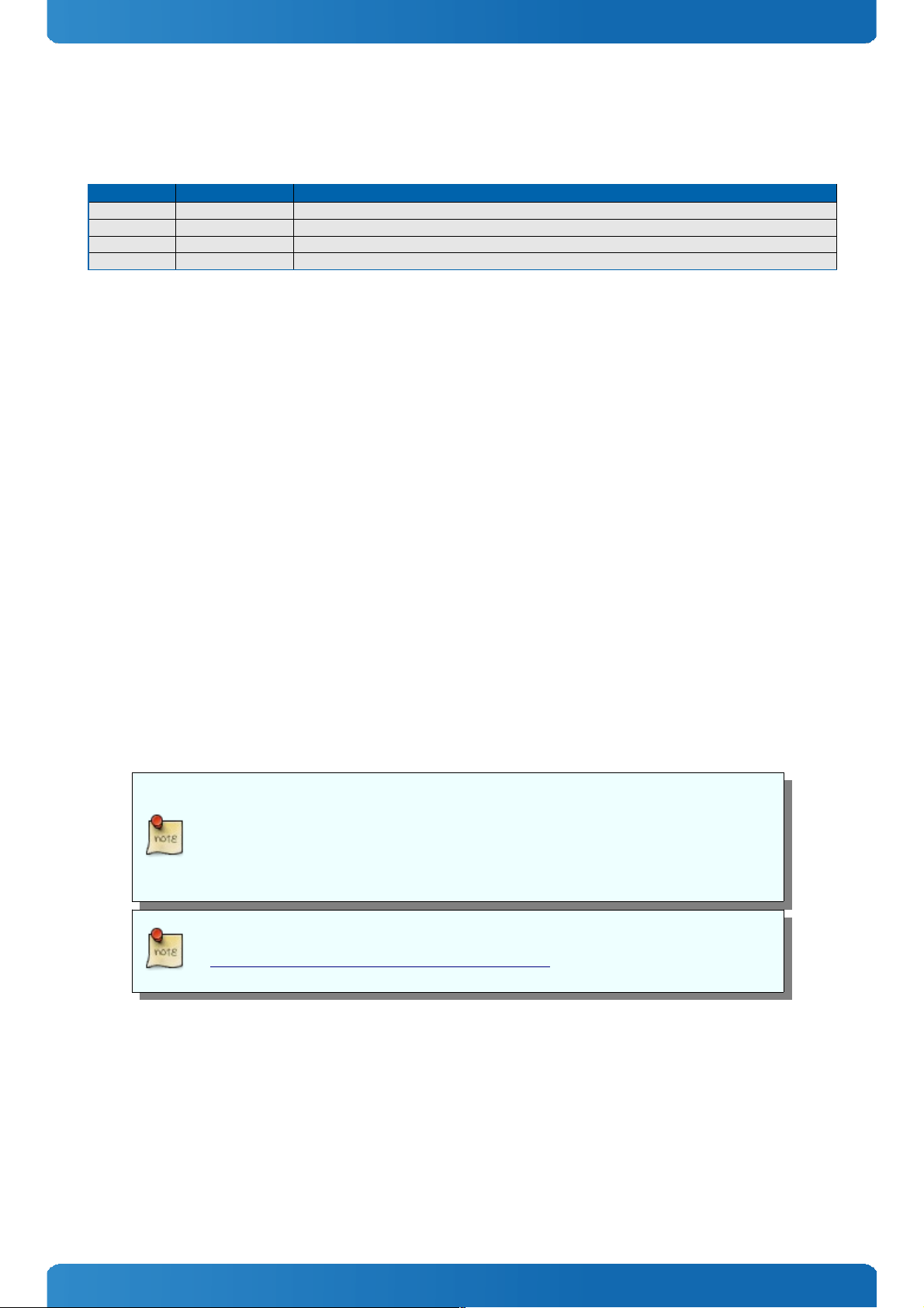
Accessories
Product Number Carrier Boards
34101-0000-00-1 COM Express® Eval Carrier Type 10
34100-0000-00-0 COM Express® Reference Carrier HMI Type 1
Product Number Cooling & Mounting
34001-0000-99-0 HSP COMe-mSP1 thread
34001-0000-99-1 HSP COMe-mSP1 through
34001-0000-99-2 HSP COMe-mSP1 slim thread
34001-0000-99-0CO1 HSK COMe-mSP1 slim passive thread
34099-0000-99-0 COMe mini Active Uni Cooler (for CPUs up to 10W)
34099-0000-99-1 COMe mini Passive Uni Cooler (for CPUs up to 5W)
34099-0000-99-2 COMe mini Passive Uni Cooler Slim (for CPUs up to 3-5W)
34017-0000-00-0 COMe mMount KIT 5/8mm 1set
Product Number Adapter & Cables
9-5000-0352 ADA-LVDS-DVI 18bit (LVDS to DVI converter)
9-5000-0353 ADA-LVDS-DVI 24bit (LVDS to DVI converter)
34120-0000-00-2 ADA-COMe-T10-T2
12
Page 13
COMe-mSP1 / Product Specification
3.2 Functional Specification
Processor
The Intel® ATOM™ (Silverthorne) CPU family supports:
» Intel® Hyper-Threading Technology
» Intel® Virtualization Technology (VT-x)
» Idle States
» Enhanced Intel SpeedStep® Technology
» Intel® Demand Based Switching
» Thermal Monitoring Technologies
» Execute Disable Bit
CPU specifications
Processor Cores / Threads CPU Clock L2 Cache Bus Speed VT-x HTT EIST Max TDP
Intel® Atom™ Z510 1 / 1 1100MHz 512KB 400MHz No No Yes 2.0W
Intel® Atom™ Z530 1 / 2 1600MHz 512KB 533MHz YES YES Yes 2.2W
Memory
Sockets
memory down
Memory Type
DDR2-533
Maximum Size
2GB
Technology
Single Channel (64bit)
The total amount of memory available on the module is used for main memory and graphics memory. The Unified Memory
Architecture (UMA) manages how the system shares memory between the graphics controller and the processor. The
maximum supported memory configuration is 8 x 2Gbit (2GB). Usually modules are equipped with 8 x 1Gbit (1GB) or 4 x
1Gbit (512MB mounted on bottom side of the PCB).
8 memory chips are only supported on hardware revision CE 4.x.x or newer. Former
hardware revisions supports up to 4x2Gbit (1GB) system memory.
13
Page 14
COMe-mSP1 / Product Specification
Graphics Core
The integrated Intel® GMA 500 based on PowerVR SGX535 core supports:
Graphics Core Render Clock
200MHz, ,
Execution Units / Pixel Pipelines
4
Max Graphics Memory
352MB
GFX Memory Bandwidth (GB/s)
4.2
GFX Memory Technology
DVMT
API (DirectX/OpenGL)
9.0c / 2.0
Shader Model
3.0
Hardware accelerated Video
H.264,MPEG2/4,VC1,WMV9
Independent/Simultaneous Displays
2 (with SDVO option)
Display Port
-
HDCP support
-
Monitor output
CRT max Resolution
-
TV out:
-
LVDS
LVDS Bits/Pixel
1x18 / 1x24
LVDS Bits/Pixel with dithering
-
LVDS max Resolution:
1366x768, 112MHz
PWM Backlight Control:
YES
Supported Panel Data:
JILI2/JILI3/EDID/DID
Display Interfaces
Discrete Graphics
-
Digital Display Interface DDI1
SDVOB optional
Digital Display Interface DDI2
-
Digital Display Interface DDI3
-
Maximum Resolution on DDI
1600x1200
Chipset
The 130nm Intel System Controller Hub Poulsbo supports:
» PCI Express Revision 1.0
» USB 2.0
» USB Client
» SDIO 1.0
Storage
onboard SSD
512MB to 8GB SLC (PATA)
SD Card support
SD 1.1 shared with GPIO
IDE Interface
-
Serial-ATA
1x SATA 1.5GB/s
SATA AHCI
-
SATA RAID
-
When using a hard disk on SATA #0 as primary device for the operating system the boot
order should be changed according the usage. Wrong boot order may cause problems
writing the MBR during OS installation.
14
Page 15
COMe-mSP1 / Product Specification
Connectivity
USB
8x USB 2.0
USB Client
1x USB Client (USB #7)
PCI
-
PCI External Masters
-
PCI Express
1x PCIe x1 Gen1
Max PCI Express
2x PCIe x1 without LAN
PCI Express x2/x4 configuration
-
Ethernet
10/100/1000 Mbit
Ethernet controller
Intel® 82574L (Hartwell)
Express Card Hot-plug is not supported by US15W SCH
Ethernet
The Intel® 82574L (Hartwell) ethernet supports:
» Jumbo Frames
» Time Sync Protocol Indicator
» WOL (Wake On LAN)
» PXE (Preboot eXecution Environment)
Misc Interfaces and Features
Audio
HD Audio
Onboard Hardware Monitor
WINBOND W83L771W
Trusted Platform Module
Infineon TPM 1.2 SLB9635TT optional
Miscellaneous
-
TPM is only available on customized variants and requires BIOS NOW1R118 or newer. With
TPM option booting from external LPC FWH is not supported
Kontron Features
External I2C Bus
Fast I2C
M.A.R.S. support
YES
Embedded API
JIDA16 / JIDA32
Custom BIOS Settings / Flash Backup
YES
Watchdog support
Single Staged
Power Features
Singly Supply Support
YES
Supply Voltage
4.75 - 14V
ACPI
ACPI 3.0
S-States
S0, S3, S4, S5
S5 Eco Mode
-
Misc Power Management
-
15
Page 16
COMe-mSP1 / Product Specification
Power Consumption and Performance
Full Load Power Consumption
4.9 - 6.2W
Kontron Performance Index
1108 - 1687
Kontron Performance/Watt
225 - 273
Detailed Power Consumption measurements in all states and bechmarks for CPU, Graphics
and Memory performance are available in Application Note KEMAP054 at EMD Customer
Section.
Supported Operating Systems
The COMe-mSP1 supports:
» Microsoft Windows XP x86
» Microsoft Windows 7 x86
» Microsoft Windows Embedded Standard 7
» Microsoft Windows CE 6.0
» Microsoft Windows XP embedded
» Linux
» WindRiver VxWorks
» QNX Neutrino
16
Page 17
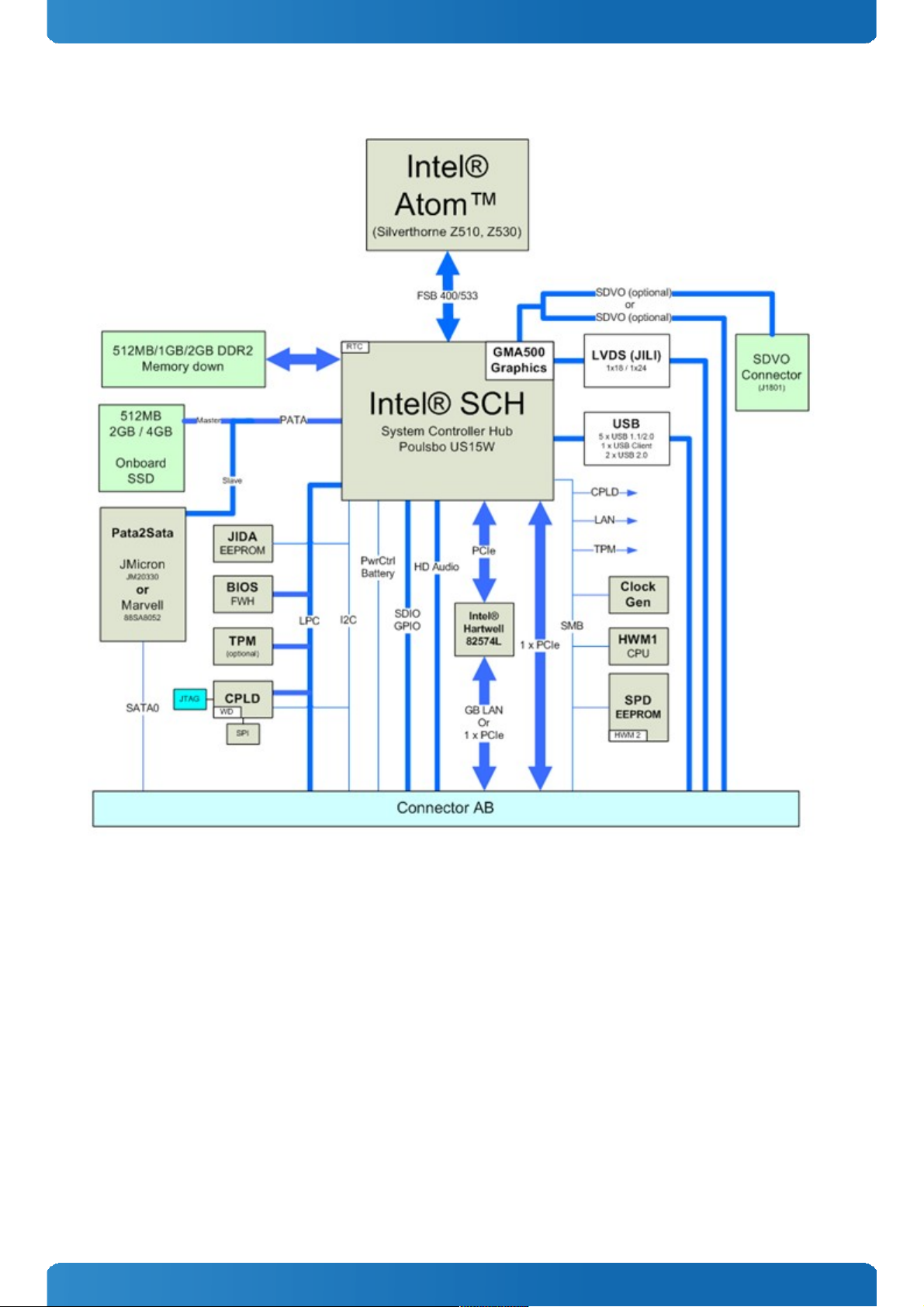
COMe-mSP1 / Product Specification
3.3 Block Diagram
17
Page 18
COMe-mSP1 / Product Specification
3.4 Electrical Specification
3.4.1 Supply Voltage
Following supply voltage is specified at the COM Express® connector:
VCC:
4.75 - 14V
Standby:
5V DC +/- 5%
RTC:
2.5V - 3.3V
- 5V Standby voltage is not mandatory for operation.
- Extended Temperature (E1) variants are validated for 12V supply only
3.4.2 Power Supply Rise Time
» The input voltages shall rise from ≤10% of nominal to within the regulation ranges within 0.1ms to 20ms.
» There must be a smooth and continuous ramp of each DC input voltage from 10% to 90% of its final set-point
following the ATX specification
3.4.3 Supply Voltage Ripple
» Maximum 100 mV peak to peak 0 – 20 MHz
3.4.4 Power Consumption
The maximum Power Consumption of the different COMe-mSP1 variants is 4.9 - 6.2W (100% CPU load on all cores; 90°C
CPU temperature). Further information with detailed measurements are available in Application Note KEMAP054 available
on EMD Customer Section. Information there is available after registration.
18
Page 19
COMe-mSP1 / Product Specification
3.4.5 ATX Mode
By connecting an ATX power supply with VCC and 5VSB, PWR_OK is set to low level and VCC is off. Press the Power Button to
enable the ATX PSU setting PWR_OK to high level and powering on VCC. The ATX PSU is controlled by the PS_ON# signal
which is generated by SUS_S3# via inversion. VCC can be 4.75 - 14V in ATX Mode. On Computer-on-Modules supporting a
wide range input down to 4.75V the input voltage shall always be higher than 5V Standby (VCC > 5VSB).
State PWRBTN# PWR_OK V5_StdBy PS_ON# VCC
G3 x x 0V x 0V
S5 high low 5V high 0V
S5 S0 → PWRBTN Event low high → 5V high low → 0 V VCC →
S0 high high 5V low VCC
3.4.6 Single Supply Mode
In single supply mode (or automatic power on after power loss) without 5V Standby the module will start automatically
when VCC power is connected and Power Good input is open or at high level (internal PU to 3.3V). PS_ON# is not used in
this mode and VCC can be 4.75 - 14V.
To power on the module from S5 state press the power button or reconnect VCC. Suspend/Standby States are not
supported in Single Supply Mode.
State PWRBTN# PWR_OK V5_StdBy VCC
G3 x x x 0
G3 S0 → high open / high x connecting VCC
S5 high open / high x VCC
S5 S0 → PWRBTN Event open / high x reconnecting VCC
Signals marked with “x” are not important for the specific power state. There is no
difference if connected or open.
All ground pins have to be tied to the ground plane of the carrier board.
19
Page 20
COMe-mSP1 / Product Specification
3.5 Power Control
Power Supply
The COMe-mSP1 supports a power input from 4.75 - 14V. The supply voltage is applied through the VCC pins (VCC) of the
module connector.
Power Button (PWRBTN#)
The power button (Pin B12) is available through the module connector described in the pinout list. To start the module via
Power Button the PWRBTN# signal must be at least 50ms (50ms ≤ t < 4s, typical 400ms) at low level (Power Button Event).
Pressing the power button for at least 4seconds will turn off power to the module (Power Button Override).
Power Good (PWR_OK)
The COMe-mSP1 provides an external input for a power-good signal (Pin B24). The implementation of this subsystem
complies with the COM Express® Specification. PWR_OK is internally pulled up to 3.3V and must be high level to power on
the module.
Reset Button (SYS_RESET#)
The reset button (Pin B49) is available through the module connector described in the pinout list. The module will stay in
reset as long as SYS_RESET# is grounded. If available, the BIOS setting for “Reset Behavior” must be set to “Power Cycle”.
Modules with Intel® Chipset and active Management Engine does not allow to hold the
module in Reset out of S0 for a long time. At about 10s holding the reset button the ME will
reboot the module automatically
SM-Bus Alert (SMB_ALERT#)
With an external battery manager present and SMB_ALERT# (Pin B15) connected the module always powers on even if
BIOS switch “After Power Fail” is set to “Stay Off”.
20
Page 21
COMe-mSP1 / Product Specification
3.6 Environmental Specification
3.6.1 Temperature Specification
General Specification Operating Non-operating
Commercial grade 0°C to +60°C -30°C to +85°C
Extended (E1) -25°C to +75°C -30°C to +85°C
Industrial grade (E2) -40°C to +85°C -40°C to +85°C
Standard modules are available for commercial grade temperature range. Please see
chapter Product Specification for available variants for extended or industrial temperate
grade
With Kontron heatspreader plate assembly
The operating temperature defines two requirements:
» the maximum ambient temperature with ambient being the air surrounding the module.
» the maximum measurable temperature on any spot on the heatspreader's surface
Without Kontron heatspreader plate assembly
The operating temperature is the maximum measurable temperature on any spot on the module's surface.
3.6.2 Humidity
» Operating: 10% to 90% (non condensing)
» Non operating: 5% to 95% (non condensing)
21
Page 22
COMe-mSP1 / Product Specification
3.7 Standards and Certifications
RoHS
The COMe-mSP1 is compliant to the directive 2002/95/EC on the restriction of the use of certain hazardous substances
(RoHS) in electrical and electronic equipment.
CE marking
The COMe-mSP1 is CE marked according to Low Voltage Directive 2006/95/EC – Test standard EN60950
Component Recognition UL 60950-1
The COM Express® mini form factor Computer-on-Modules are Recognized by Underwriters Laboratories Inc.
Representative samples of this component have been evaluated by UL and meet applicable UL requirements.
UL Listings:
» NWGQ2.E304278
» NWGQ8.E304278
WEEE Directive
WEEE Directive 2002/96/EC is not applicable for Computer-on-Modules.
Conformal Coating
Conformal Coating is available for Kontron Computer-on-Modules and for validated SO-DIMM memory modules. Please
contact your local sales or support for further details.
22
Page 23

COMe-mSP1 / Product Specification
Shock & Vibration
The COM Express® mini form factor Computer-on-Modules successfully passed shock and vibration tests according to
» IEC/EN 60068-2-6 (Non operating Vibration, sinusoidal, 10Hz-4000Hz, +/-0.15mm, 2g)
» IEC/EN 60068-2-27 (Non operating Shock Test, half-sinusoidal, 11ms, 15g)
EMC
Validated in Kontron reference housing for EMC the COMe-mSP1 follows the requirements for electromagnetic
compatibility standards
» EN55022
23
Page 24
COMe-mSP1 / Product Specification
3.8 MTBF
The following MTBF (Mean Time Before Failure) values were calculated using a combination of manufacturer’s test data, if
the data was available, and the Telcordia (Bellcore) issue 2 calculation for the remaining parts.
The calculation methode used is “Telcordia Method 1 Case 3” in a ground benign, controlled environment (GB,GC). This
particular method takes into account varying temperature and stress data and the system is assumed to have not been
burned in.
Other environmental stresses (extreme altitude, vibration, salt water exposure, etc) lower MTBF values.
System MTBF (hours): 209423 @ 40°C
Fans usually shipped with Kontron Europe GmbH products have 50,000-hour typical
operating life. The above estimates assume no fan, but a passive heat sinking arrangement
Estimated RTC battery life (as opposed to battery failures) is not accounted for in the above
figures and need to be considered for separately. Battery life depends on both temperature
and operating conditions. When the Kontron unit has external power; the only battery
drain is from leakage paths.
24
Page 25
COMe-mSP1 / Product Specification
3.9 Mechanical Specification
3.9.1 Module Dimension
» 55mm x 84mm (±0.2mm)
3.9.2 Height on Top
» Maximum approx. 3.5mm (withouth printed circuit board)
» Height is depending on (optional) CPU cooler / heat spreader
3.9.3 Height on Bottom
» Maximum approx. 3.5mm (without printed circuit board)
3.9.4 Mechanical Drawing
All dimensions are shown in millimeters. Tolerances should be ± 0.25mm [±0.010”], unless otherwise noted. The
tolerances on the module connector locating peg holes (dimensions [16.50, 6.00]) should be ± 0.10mm [±0.004”]. The
220 pin module connector shall be mounted on the backside of the PCB and is seen “through” the board in this view. The 4
mounting holes shown in the drawing should use 6mm diameter pads and should have 2.7mm plated holes, for use with
2.5mm hardware. The pads should be tied to the PCB ground plane.
CAD drawings are available at EMD CustomerSection
25
Page 26

COMe-mSP1 / Product Specification
3.10 Thermal Management
A heatspreader plate assembly is available from Kontron Europe GmbH for the COMe-mSP1. The heatspreader plate on top
of this assembly is NOT a heat sink. It works as a COM Express®-standard thermal interface to use with a heat sink or other
cooling device.
External cooling must be provided to maintain the heatspreader plate at proper operating temperatures. Under worstcase conditions, the cooling mechanism must maintain an ambient air and heatspreader plate temperature of 60° C or
less.
The aluminum slugs and thermal pads on the underside of the heatspreader assembly implement thermal interfaces
between the heatspreader plate and the major heat-generating components on the COMe-mSP1. About 80 percent of the
power dissipated within the module is conducted to the heatspreader plate and can be removed by the cooling solution.
You can use many thermal-management solutions with the heatspreader plates, including active and passive approaches.
The optimum cooling solution varies, depending on the COM Express® application and environmental conditions. Please
see the COM Express® Design Guide for further information on thermal management.
3.11 Heatspreader
Documentation and CAD drawings of COMe-mSP1 heatspreader and cooling solutions is provided at
http://emdcustomersection.kontron.com.
26
Page 27
COMe-mSP1 / Features and Interfaces
4 Features and Interfaces
4.1 Onboard SSD
The COMe-mSP1 features an onboard Greenliant PATA NAND flash drive with capacities of 512MB to 8GB SLC (PATA). Due to
performance and longevity reasons standard variants with onboard flash use SLC type only. The following PATA NANDrives
are available:
Basic features of the PATA NANDrives
» 16-bit ATA/IDE Bus Interface with PIO Mode-6, Multi-Word DMA Mode-4 and Ultra DMA Mode-4
» RoHS compliant NAND flash type
» Hardware error detection and correction ECC
» Advanced wear leveling
» Bad block management
SLC NANDrive™
Flash Part No. GLS85LP0512P-S-I-LBTE GLS85LP1002P-S-I-FTE GLS85LP1004P-S-I-FTE GLS85LP1008P-S-I-FTE
Temperature Range
-40°C to +85°C -40°C to +85°C -40°C to +85°C -40°C to +85°C
Flash Size 512MB 2GB 4GB 8GB
NAND Type
SLC NAND SLC NAND SLC NAND SLC NAND
Sustained Read Speed
25 MB/s 28 MB/s 50 MB/s 50 MB/s
Sustained Write Speed
6 MB/s 11 MB/s 20 MB/s 39 MB/s
Total Bytes
456,744,960 2,000,388,096 4,068,384,768 8,136,769,536
Max LBA
892,080 3,907,008 7,946,064 15,892,128
Cylinders/Heads/Sectors
885/16/63 3,876/16/63 7,883/16/63 15,766/16/63
Active Mode Power
200mW 200mW 265mW 365mW
Program/Erase Cycles per Block
100k 100k 100k 100k
(Data based on GLS85LPxxxxP Datasheet Rev. 02.000 from 06-2012)
The NAND Flash types listed above are available on COMe-mSP1 hardware revision CE4.7.0
and COMe-cDC2 hardware revision CE 2.4.1 or newer. Please contact your local sales or
support for Flash specifications of SST Flash used on older revisions
27
Page 28
COMe-mSP1 / Features and Interfaces
4.2 LPC
The Low Pin Count (LPC) Interface signals are connected to the LPC Bus bridge located in the CPU or chipset. The LPC low
speed interface can be used for peripheral circuits such as an external Super I/O Controller, which typically combines
legacy-device support into a single IC. The implementation of this subsystem complies with the COM Express®
Specification. Implementation information is provided in the COM Express® Design Guide maintained by PICMG. Please
refer to the official PICMG documentation for additional information.
The LPC bus does not support DMA (Direct Memory Access) and a clock buffer is required when more than one device is
used on LPC. This leads to limitations for ISA bus and SIO (standard I/O´s like Floppy or LPT interfaces) implementations.
All Kontron COM Express® Computer-on-Modules imply BIOS support for following external baseboard LPC Super I/O
controller features for the Winbond/Nuvoton 5V 83627HF/G and 3.3V 83627DHG-P:
83627HF/G Phoenix BIOS AMI CORE8 AMI Aptio
PS/2 YES YES YES
COM1/COM2 YES YES YES
LPT YES YES YES
HWM YES YES NO
Floppy NO NO NO
GPIO NO NO NO
83627DHG-P Phoenix BIOS AMI CORE8 AMI Aptio
PS/2 YES YES YES
COM1/COM2 YES YES YES
LPT YES YES YES
HWM NO NO NO
Floppy NO NO NO
GPIO NO NO NO
Features marked as not supported do not exclude OS support (e.g. HWM can be accessed via SMB). For any other LPC
Super I/O additional BIOS implementations are necessary. Please contact your local sales or support for further details.
28
Page 29
COMe-mSP1 / Features and Interfaces
4.3 LPC boot
The COMe-mSP1 supports boot from an external Firmwarehub on LPC bus (LPC FWH). The external LPC FWH can be
activated with signal A34 “BIOS_DISABLE#” or according newer specifications “BIOS_DIS0#” in following configuration:
BIOS_DIS0# BIOS_DIS1# Function
open open Boot on-module BIOS
GND open Boot baseboard LPC FWH
open GND Baseboard SPI = Boot Device 1, on-module SPI = Boot Device 2
GND GND Baseboard SPI = Boot Device 2, on-module SPI = Boot Device 1
Using an external LPC Firmware Hub
To program an external LPC FWH follow these steps:
» Connect a 1MB LPC FWH to the module's LPC interface
» Open pin A34 to boot from the module BIOS
» Boot the module to DOS with access to the BIOS image and Firmware Update Utility aufdos.exe / batch file provided
on EMD Customer Section
» Connect pin A43 (BIOS_DIS0#) to ground to enable the external LPC FWH
» Execute Flash.bat to flash the BIOS image to the external LPC FWH
» reboot
Your module will now boot from the external LPC FWH when BIOS_DIS0# is grounded.
To create a BIOS with custom defaults:
» Change your BIOS settings
» Save as custom defaults to RTC/Flash and Exit (module will now always start with these settings)
» Extract the BIOS including custom defaults with afudos.exe biosname.rom /O in DOS or kflash.exe backup
biosname.rom in Windows
Flash Backup should show “Enter new Password” first time saving custom defaults. If it is
not possible to set a new password or entering a password shows an error message, please
clean up CMOS data with DOS command: jidacmos rtc /clean (jidacmos utility is available
at Kontron’s Customer Section)
You can download all AMI CORE8 update utilities at AMI.com:
http://www.ami.com/support/downloads/amiflash.zip
29
Page 30

COMe-mSP1 / Features and Interfaces
4.4 M.A.R.S.
The Smart Battery implementation for Kontron Computer-on-Modules called Mobile Application for Rechargeable Systems
is a BIOS extension for external Smart Battery Manager or Charger. It includes support for SMBus charger/selector (e.g.
Linear Technology LTC1760 Dual Smart Battery System Manager) and provides ACPI compatibility to report battery
information to the Operating System.
Reserved SM-Bus addresses for Smart Battery Solutions on the carrier:
8-bit Address 7-bit Address Device
12h 0x09 SMART_CHARGER
14h 0x0A SMART_SELECTOR
16h 0x0B SMART_BATTERY
30
Page 31

COMe-mSP1 / Features and Interfaces
4.5 Fast I2C & SMBus
The COMe-mSP1 integrates two configurable I2C buses. The external I2C provided via US15W GPIOs on COM Express®
Connector Pin B33/B34, the LVDS I2C from US15W SCH is available on COM express® connector pin A83/A84. The I2C
interface offers full MultiMaster and Clock Stretching support. Fast I2C and SMBus clock speed depends on the CPU
performance and differs between ATOM™ Z510 and ATOM™ Z530 modules. See the tables below for measured values on
COMe-mSP1 with BIOS NOW1R118.
JIDA/external I2C speed
JIDA/external I2C speed JILI I2C speed SMBus speed
Setup ATOM™ Z510 ATOM™ Z530 ATOM™ Z510 ATOM™ Z530 ATOM™ Z510 ATOM™ Z530
Extra high not suppor ted not supported not supported not supported 375 kHz 418 kHz
Very high 166 kHz 215 kHz 80 kHz 125 kHz 214 kHz 270 kHz
High 80 kHz 110 kHz 55 kHz 80 kHz 57 kHz 86 kHz
Medium 41 kHz 60 kHz 34 kHz 50 kHz 35 kHz 46 kHz
Slow 10 kHz 15 kHz 9.6 kHz 15 kHz 7.4 kHz 10 kHz
Very slow 1 kHz 2 kHz 1.5 kHz 2 kHz 0.7 kHz 1 kHz
Ultra slow 0.7 kHz 1 kHz not supported not suppor ted not supported not suppor ted
31
Page 32

COMe-mSP1 / Features and Interfaces
4.6 JIDA16 and JIDA32
JIDA16 (JUMPtec® Intelligent Device Architecture) is a BIOS interface which allows programs running in Real Mode
operating systems (i.e. MS DOS) to call certain functions implemented in the BIOS. These functions can be used to get
module information, make settings and access the I2C Bus and the Watchdog unit. JIDA16 functions are INT 15h BIOS calls
which are only available in 16 Bit Real Mode operating systems.
For 32bit operating systems (i.e. WindowsXP, Windows 7, Windows CE, VxWorks, Linux) a different JIDA implementation
called JIDA32 is implemented. The same common driver for all JIDA32 capable modules talks to the JIDA32 part in the
BIOS, which is hardware dependent to interact with the hardware.
Please refer to EMD Customer Section for detailed documentation, JIDA utilities and Libraries for DOS, Windows, Linux,
VxWorks or QNX.
Usage of JIDA16 and JIDA32
32
Page 33

COMe-mSP1 / Features and Interfaces
4.7 K-Station 1
Based on the JIDA32 interface users can implement advanced board functionality in their application. As an example
utility Kontron provides K-Station for most 32bit Windows Operating Systems. K-Station 1 is a summary of command line
utilities (Shell Tools) for easy access to JIDA32 BIOS implementations. Second part of K-Station is a JAVA based example
GUI which gives a view an all available features using the Shell Tools.
Following K-Station Shell Tools are available:
» KSystemSummary.exe (System Information)
» KGenInfo.exe (Module Information)
» KCPUPerf.exe (CPU Throttling control)
» KHWMon.exe (Hardware Monitoring)
» KI2CBus.exe (I2C and SMBus access)
» KIOPort.exe (GPIO control)
» KStorage.exe (JIDA EEPROM access to user bytes)
» KVGATool.exe (LVDS Backlight control)
» KWDog.exe (Watchdog control)
» KAMIMod.exe (AMICore8 BIOS Modification with Bootlogo or Usercode …)
» KFlash.exe (AMICore8 BIOS Update)
The full K-Station package, the stand-alone Shell Tools with drivers, example batch files and documentation is available
on EMD Customer Section for free.
33
Page 34

COMe-mSP1 / Features and Interfaces
4.8 K-Station & API Resources
4.8.1 I2C
BUS Function
I2C 0 External / JIDA I2C
I2C 1 SM-Bus
I2C 2 SDVO DDC
I2C 3 JILI DDC
4.8.2 Storage
Device Function
EEPROM 0 JIDA EEPROM Area1 with 32 Bytes (free to use)
4.8.3 GPIO
Port Function
IO-Port 0 GPI0 Port, Bit 0-3: Input, Bit 4-7: Output Direction Change possible with NOW1R117 and CE 4.6.0 or newer
4.8.4 Hardware Monitor
Sensor Function
Temp 0 Module Temperature (internal IC temperature of onboard Winbond W839771 HWM)
Temp 1 CPU ACPI Temperature (measured with Winbond W839771 HWM))
Temp 2 External SIO Winbond 83627 Temp Sensor 1)
Temp 3 External SIO Winbond 83627 Temp Sensor 2
Temp 4 External SIO Winbond 83627 Temp Sensor 3
FAN 0 External SIO Winbond 83627 FAN Sensor 0
FAN 1 External SIO Winbond 83627 FAN Sensor 1
FAN 2 External SIO Winbond 83627 FAN Sensor 2
Voltage 0 External SIO Winbond 83627 Voltage Sensor 0: CoreA
Voltage 1 External SIO Winbond 83627 Voltage Sensor 1: CoreB
Voltage 2 External SIO Winbond 83627 Voltage Sensor 2: 3.3V Battery
Voltage 3 External SIO Winbond 83627 Voltage Sensor 3: +3.3V
Voltage 4 External SIO Winbond 83627 Voltage Sensor 4: +5V
Voltage 5 External SIO Winbond 83627 Voltage Sensor 5: +5V_SB
Voltage 6 External SIO Winbond 83627 Voltage Sensor 6: +12V
Voltage 7 External SIO Winbond 83627 Voltage Sensor 7: -5V
Voltage 8 External SIO Winbond 83627 Voltage Sensor 8: -12V
34
Page 35

COMe-mSP1 / Features and Interfaces
4.9 GPIO - General Purpose Input and Output
The offers 4 General Purpose Input (GPI) pins and 4 General Purpose Output (GPO) pins. On a 3.3V level digital in- and
outputs are available.
Signal Pin Description
GPI0 A54 General Purpose Input 0
GPI1 A63 General Purpose Input 1
GPI2 A67 General Purpose Input 2
GPI3 A85 General Purpose Input 3
GPO0 A93 General Purpose Output 0
GPO1 B54 General Purpose Output 1
GPO2 B57 General Purpose Output 2
GPO3 B63 General Purpose Output 3
Configuration
The GPI and GPO pins can be configured via JIDA32/K-Station. Please refer to the JIDA32/K-Station manual in the driver
download packet on our customer section.
To enable GPIO functionality, modules with HW revision CE 1.x.x must be reworked. Contact
your local sales or support for further information. On modules with HW revision CE 4.x.x
and BIOS R115 or newer GPIO/SDIO can be switched via BIOS setup option
The General Purpose Inputs and Outputs are not applicable to drive applications faster than
2ms. It’s recommended to use data transfer rates only up to 1 kHz.
General Purpose Outputs are high impedance until first write access
There is one IO Port controlled via onboard CPLD (1 Byte, Port 0) available and the 4 Inputs and 4 Outputs are fixed in
direction. To access the GPIOs use the JIDA32 interface. You can write to a General Purpose Output with the upper half
byte. To read a General purpose Input use the lower half byte.
Bit of GPIO Port0 Function COM Express Pin
0 GPI0 A54
1 GPI1 A63
2 GPI2 A67
3 GPI3 A85
4 GPO0 A93
5 GPO1 B54
6 GPO2 B57
7 GPO3 B63
35
Page 36

COMe-mSP1 / Features and Interfaces
4.10 Watchdog Timer
You can configure the Watchdog Timer (WDT) in BIOS setup to start after a set amount of time after power-on boot. The
WDT can also be controlled by the JIDA32 Library API. The application software should strobe the WDT to prevent its
timeout. Upon timeout, the WDT resets and restarts the system. This provides a way to recover from program crashes or
lockups.
Configuration
You can program the timeout period for the watchdog timer in two ranges:
» 1-second increments from 1 to 255 seconds
» 1-minute increments from 1 to 255 minutes
Contact Kontron Embedded Modules technical support for information on programming and operating the WDT.
36
Page 37

COMe-mSP1 / Features and Interfaces
4.11 Flash Backup Feature
The COMe-mSP1 supports a new functionality called “Flash Backup”. This new feature allows saving custom defaults
directly into the Flash. With invalid EEPROM data or without a CMOS EEPROM, the module will start up with these custom
defaults. It’s possible to save this BIOS with changed defaults to an image and flash it on other modules.
To create a BIOS with custom defaults:
» Change your BIOS settings
» Save as custom defaults to RTC/Flash and Exit (module will now always start with these settings)
Flash Backup should show “Enter new Password” first time saving custom defaults. If it is
not possible to set a new password or entering a password shows an error message, please
clean up CMOS data with DOS command: jidacmos rtc /clean (jidacmos utility is available
at Kontron’s Customer Section)
» Extract the BIOS including custom defaults with afudos or kflash utility for windows
Tool Command
AFUDOS
c:\>afudos.exe biosname.rom /O
KFLASH
c:\>kflash.exe backup biosname.rom
37
Page 38

COMe-mSP1 / Features and Interfaces
Flash your BIOS with custom defaults:
To flash a BIOS with customized defaults extracted like described above, use following options
Operating System Command
Windows OS
c:\>kflash.exe flash biosname.rom /bncr
DOS
c:\>afudos.exe biosname.rom /p /b /n /c
c:\>jidacmos.exe eep /clean
kflash.exe is a shell tool included in Kontron K-Station System Utility Package.
jidacmos utility is included in the BIOS download packages at Kontron's customer section.
38
Page 39

COMe-mSP1 / Features and Interfaces
4.12 Speedstep Technology
The Intel® processors offers the Intel® Enhanced SpeedStep™ technology that automatically switches between maximum
performance mode and battery-optimized mode, depending on the needs of the application being run. It let you
customize high performance computing on your applications. When powered by a battery or running in idle mode, the
processor drops to lower frequencies (by changing the CPU ratios) and voltage, conserving battery life while maintaining
a high level of performance. The frequency is set back automatically to the high frequency, allowing you to customize
performance.
In order to use the Intel® Enhanced SpeedStep™ technology the operating system must support SpeedStep™ technology.
By disabling the SpeedStep feature in the BIOS, manual control/modification of CPU performance is possible. Setup the
CPU Performance State in the BIOS Setup or use 3rd party software to control CPU Performance States.
39
Page 40

COMe-mSP1 / Features and Interfaces
4.13 C-States
New generation platforms include power saving features like SuperLFM, EIST (P-States) or C-States in O/S idle mode.
Activated C-States are able to dramatically decrease power consumption in idle mode by reducing the Core Voltage or
switching of parts of the CPU Core, the Core Clocks or the CPU Cache.
Following C-States are defined:
C-State Description Function
C0 Operating CPU fully turned on
C1 Halt State Stops CPU main internal clocks via software
C1E Enhanced Halt Similar to C1, additionally reduces CPU voltage
C2 Stop Grant Stops CPU internal and external clocks via hardware
C2E Extended Stop Grant Similar to C2, additionally reduces CPU voltage
C3 Deep Sleep Stops all CPU internal and external clocks
C3E Extended Stop Grant Similar to C3, additionally reduces CPU voltage
C4 Deeper Sleep Reduces CPU voltage
C4E Enhanced Deeper Sleep Reduces CPU voltage even more and turns of f the memory cache
C6 Deep Power Down Reduces the CPU internal voltage to any value, including 0V
C7 Deep Power Down Similar to C6, additionally LLC (LastLevelCache) is switched off
C-States are usually enabled by default for low power consumption, but active C-States my influence performance
sensitive applications or real-time systems.
» Active C6-State may influence data transfer on external Serial Ports
» Active C7-State may cause lower CPU and Graphics performance
It's recommended to disable C-States / Enhanced C-States in BIOS Setup if any problems occur.
40
Page 41

COMe-mSP1 / Features and Interfaces
4.14 Hyper Threading
Hyper Threading (officially termed Hyper Threading Technology or HTT) is an Intel®-proprietary technology used to
improve parallelization of computations performed on PC´s. Hyper-Threading works by duplicating certain sections of the
processor—those that store the architectural state but not duplicating the main execution resources. This allows a HyperThreading equipped processor to pretend to be two “logical” processors to the host operating system, allowing the
operating system to schedule two threads or processes simultaneously. Hyper Threading Technology support always relies
on the Operating System.
41
Page 42

COMe-mSP1 / Features and Interfaces
4.15 ACPI Suspend Modes and Resume Events
The COMe-mSP1 supports the S3 state (=Save to Ram). S4 (=Save to Disk) is not supported by the BIOS (S4_BIOS) but
S4_OS is supported by the following operating systems:
» Windows XP
» Windows Vista
» Windows 7
The following events resume the system from S3:
» USB Keyboard (1)
» USB Mouse (1)
» Power Button
» WakeOnLan (2)
The following events resume the system from S4:
» Power Button
» WakeOnLan (2)
The following events resume the system from S5:
» Power Button
» WakeOnLan (2)
(1) OS must support wake up via USB devices and baseboard must power the USB Port with
StBy-Voltage
(2) WakeOnLan must be enabled in BIOS setup and driver options
42
Page 43

COMe-mSP1 / Features and Interfaces
4.16 USB
The USB interface comes with three USB controllers (6 USB ports). The USB configuration of the COMe-mSP1 module is
described in the following table:
COM Express Port SCH US15W Port Description
USB0 USB0 USB 2.0 compliant
USB1 USB1 USB 2.0 compliant
USB2 USB4 USB 2.0 compliant
USB3 USB5 USB 2.0 compliant
USB4 USB6 Not USB 2.0 compliant, no UHCI controller (no USB 1.1 / USB 2.0 only)
USB5 USB7 Not USB 2.0 compliant, no UHCI controller (no USB 1.1 / USB 2.0 only)
USB6 USB3 USB 2.0 compliant
USB7 USB2 USB Client or USB 2.0 compliant port (configurable in BIOS Setup)
Internal USB mapping from US15W SCH
USB Client Port
The USB interface supports also one USB client port (USB port 7) that can be activated in setup. If the client function is
disabled in the BIOS this port acts as a normal USB 2.0 port. Please be aware that USB power lines may not be connected
on the USB client port.
Special USB client and host driver software is needed for USB client function. When this
driver and software is installed the client port appears as a mass storage device and NDIS
Network device or as NDIS Network device only in the device manager of the operating
system. Please refer to the Kontron COMe-mSP1 download page for the driver
43
Page 44

COMe-mSP1 / Features and Interfaces
4.17 SDIO
The SD card standard is a standard for removable memory storages designed and licensed by the SD Card Association
(http://sdcard.org). The card form factor, electrical interface, and protocol are all part of the SD Card specification. The
Intel® System Controller Hub US15W supports up to 3 SDIO interfaces. On nanoETXexpress-SP the first interface SDIO#0
(4-bit wide) is shared with the module GPIO signals. The integrated SDIO 1.1/MMC 4.1 controller in US15W only supports
byte-address mode for SDIO storage cards up to 2GB. Sector-addressing and SDHC is not supported.
» MMC 4.1 transfer rates can be up to 48MHz and bus widths of 1, 4 or 8 bits
» SDIO 1.1 supports transfer rates up to 24MHz and bus widths of 1 or 4 bits
The following table shows which GPIO-ports can be used for the SD-card interface:
General purpose Input/output SD card interface signals
GPI0 SLOT0_DATA0
GPI1 SLOT0_DATA1
GPI2 SLOT0_DATA2
GPI3 SLOT0_DATA3
GPO0 SLOT0_CLK
GPO1 SLOT0_CMD
GPO2 SLOT0_WP
GPO3 SLOT0_CD#
The SD_CMD line needs a pull-up resistor that can vary depending on the length of the
electrical paths (typical from 10kOhm to 100kOhm).
The maximum length for SDIO signals on the baseboard should be 80mm.
44
Page 45

COMe-mSP1 / Features and Interfaces
4.18 Graphics Interface
The COMe-mSP1 uses the graphics accelerator GMA500 with 200MHz GPU clock integrated in the Intel® System Controller
Hub (US15W), which delivers shader-based technologies and high-performance 2D, 3D and video capabilities. The
GMA500 graphics engine supports a variety of LCD panels with single clock, color depths of 18/24 bit and resolutions up
to WXGA (1366×768). The maximum supported pixelclock of the system controller hub is 112 MHz.
Hardware video decode acceleration relieves the decode burden from the processor and reduces the power consumption of
the system. Full hardware acceleration of H.264, MPEG2, VC1 and WMV9 eliminates the need of a software codec and
offloads the CPU.
The graphic adapter uses the onboard RAM as graphic memory. The preallocated memory is defined through bios settings.
Possible settings are:
» 1MB
» 4MB
» 8MB
The total amount of graphics memory in the operating system depends on the size of system memory and the used driver
settings. The graphics media accelerator driver GMA uses DVMT to manage allocating of system memory according to the
needs of running applications. The Intel® Embedded Graphics Driver IEGD allocates the maximum of graphics memory
depending on system memory and driver settings.
Physical Memory Preallocated Memory in BIOS Setup Maximum Graphics Memor y with GMA Driver Maximum Graphics Memory with IEGD
512MB 1MB 127MB 352MB
512MB 4MB 126MB 352MB
512MB 8MB 125MB 352MB
1024MB 1MB 255MB 352MB
1024MB 4MB 254MB 352MB
1024MB 8MB 253MB 352MB
For memory allocation according to the table above BIOS revision NOW1R112 or newer is
recommended
When using 1MB Preallocated Memory an Operating Systems without active GMA or IEGD
may have problems to display a screen (e.g. during WinXP installation).
45
Page 46

COMe-mSP1 / Features and Interfaces
VGA
The nanoETXexpress-SP graphics subsystem GMA500 integrated in the Intel® System Controller Hub US15W does not
support VGA output.
LVDS Flat Panel Interface (JILI)
The user interface for flat panels is the JUMPtec Intelligent LVDS Interface (JILI). The implementation of this subsystem
complies with the COM Express® Specification. Implementation information is provided in the COM Express® Design
Guide. Refer to the documentation for additional information.
SDVO
A Serial DVO connection is supported with hardware revision CE 4.x.x or newer. The digital display channel configured
from display Pipe A in GMA500 graphics adapter is capable of driving SDVO adapters that provide interfaces to a variety of
external display technologies such as HDMI, DVI, TV-out or CRT (the maximum supported pixel clock is 160MHz). Contact
your local sales representative which adapters are available.
SDVO is optional available via:
» 30pin onboard flat foil connector
» COM Express connector (recommended solution)
Alternative COM Express Pin-out with SDVO option:
Pin Standard Signal SDVO Option SDVO Option Pin Description Type SDVO Termination
B71 LVDS_B0+ SDVOB_RED_P Serial Digital Video Channel B Red+ DP-O PU 50R inUS15W
B72 LVDS_B0- SDVOB_RED_N Serial Digital Video Channel B Red- DP-O PU 50R inUS15W
B73 LVDS_B1+ SDVOB_GREEN_P Ser ial Digital Video Channel B Green+ DP-O PU 50R inUS15W
B74 LVDS_B1- SDVOB_GREEN_N Serial Digital Video Channel B Green- DP-O PU 50R inUS15W
B75 LVDS_B2+ SDVOB_BLUE_P Serial Digital Video Channel B Blue+ DP-O PU 50R inUS15W
B76 LVDS_B2- SDVOB_BLUE_N Serial Digital Video Channel B Blue- DP-O PU 50R inUS15W
B77 LVDS_B3+ SDVOB_INT_P Serial Digital Video Input Interrupt+ DP-I PD 50R inUS15W
B78 LVDS_B3- SDVOB_INT_N Serial Digit al Video Input Interrupt- DP-I PD 50R inUS15W
.. .. .. .. .. ..
B81 LVDS_B_CK+ SDVOB_CLK_P Serial Digital Video Channel B Clock+ DP-O PU 50R inUS15W
B82 LVDS_B_CK- SDVOB_CLK_N Serial Digital Video Channel B Clock- DP-O PU 50R inUS15W
.. .. .. .. .. ..
B91 VGA_GRN SDVOB_TVCLKIN_P SDVO Channel B TV-Out Sync Clock+ DP-I PD 50R inUS15W
B92 VGA_BLU SDVOB_TVCLKIN_N SDVO Channel B TV-Out Sync Clock- DP-I PD 50R inUS15W
B93 VGA_HSYNC SDVOB_STALL_P Serial Digital Video Field Stall+ DP-I PD 50R inUS15W
B94 VGA_VSYNC SDVOB_STALL_N Serial Digital Video Field Stall- DP-I PD 50R inUS15W
B95 VGA_I2C_CK SDVO_CTRLCLK SDVO Control Clock DP-I/O ..
B96 VGA_I2C_DAT SDVO_CTRLDATA SDVO Control DATA DP-I/O ..
- The SDVO option is not available on standard modules. Please contact your local sales
representative for more details or further questions.
- The optional SDVO pinout is similar to Type 10 pin-out except SDVO Control CLK/DAT on
B95/B96 (B98/B99 on Type 10)
46
Page 47

COMe-mSP1 / Features and Interfaces
4.19 LPC Bus
The Low Pin Count Interface signals are connected to the LPC Bus bridge, which is located in the Intel® US15W system
controller hub. The LPC low speed interface can be used for peripheral circuits such as an external Super I/O Controller,
which typically combines legacy-device support into a single IC. The implementation of this subsystem complies with the
ETXexpress® Specification. Implementation information is provided in the COM Express® Design Guide by PICMG. Refer to
the documentation for additional information.
The LPC bus does not support DMA (Direct Memory Access). This leads to limitations for ISA bus and SIO (standard I/O´s
like Floppy or LPT interfaces) implementations. When more than one device is connected to the LPC bus a clock buffer is
required!
Due to Power management of the LPC Bus, clock buffers that require synchronization
should be used with great care and may prevent the board from booting up.
Active LPC Clock frequency
» with Z530 CPU: 33MHz
» with Z510 CPU: 25MHz
Standard Clock Buffer
When using a standard clock buffer on the baseboard please be aware that the generated delay has to be considered for
the length matching of the layout.
Clock Buffer Reference Schematic
The implementation of a clock buffer can be realized as shown in the evaluation schematic below:
47
Page 48

COMe-mSP1 / Features and Interfaces
Zero Delay Clock Buffer
Do not use the reference schematic in the COM Express Design Guide. Either use another
Clock Buffer solution without a long start up process or use series resistors to double the
LPC clock line. Follow the design recommendations in the COM Express Design Guide by
PICMG.
48
Page 49

COMe-mSP1 / System Resources
5 System Resources
5.1 Interrupt Request (IRQ) Lines
Please be aware that an ACPI OS decides itself on resource usage. The tables below show only an example distribution.
5.1.1 In 8259 PIC Mode
IRQ# Used For Available Comment
0 Timer 0 No -
1 Keyboard No -
2 Slave 8259 No -
3 External SIO - COM2 Yes (No) Note (1)
4 External SIO - COM1 Yes (No) Note (1)
5 PCI for PCI Dynamic (BIOS default)
6 External SIO Yes (No) Note (1)
7 External SIO - LPT1 Yes (No) Note (1)
8 RTC No -
9 ACPI No -
10 PCI for PCI Dynamic (BIOS default)
11 PCI for PCI Dynamic (BIOS default)
12 PS/2 Mouse Yes (No) Note (1)
13 FPU No -
14 Primary IDE No Note (1)
15 PCI for PCI Dynamic (BIOS default)
(1) If the “Used For” device is disabled in setup, the corresponding interrupt is available
for other devices.
49
Page 50

COMe-mSP1 / System Resources
5.1.2 In APIC mode
IRQ# Used For Available Comment
0 Timer 0 No -
1 Keyboard No -
2 Slave 8259 No -
3 External SIO - COM2 Yes (No) Note (1)
4 External SIO - COM1 Yes (No) Note (1)
5 PCI for PCI Dynamic (BIOS default)
6 External SIO Yes (No) Note (1)
7 External SIO - LPT1 Yes (No) Note (1)
8 RTC No -
9 ACPI No -
10 PCI for PCI Dynamic (BIOS default)
11 PCI for PCI Dynamic (BIOS default)
12 PS/2 Mouse Yes (No) Note (1)
13 FPU No -
14 primar y IDE No Note (1)
15 PCI for PCI Dynamic (BIOS default)
16 PIRQ[A] For PCI PCI IRQ line 1 + US15W graphics + USB
UHCI Controller #1; Note (2)
17 PIRQ[B] For PCI PCI IRQ line 2 + LAN Controller + USB
UHCI Controller #2; Note (2)
18 PIRQ[C] For PCI PCI IRQ line 3 + USB UHCI Controller #3;
Note (2)
19 PIRQ[D] For PCI PCI IRQ line 4 + USB UHCI Controller #3;
Note (2)
20 PIRQ[E] No Note (2)
21 PIRQ[F] No Note (2)
22 PIRQ[G] No Note (2)
23 PIRQ[H] No Note (2)
(1) If the “Used For” device is disabled in setup, the corresponding interrupt is available
for other devices.
(2) ACPI Operating System decides on particular IRQ usage.
50
Page 51

COMe-mSP1 / System Resources
5.2 Memory Area
The first 640 kB of DRAM are used as main memory. Using DOS, you can address 1 MB of memory directly. Memory area
above 1 MB (high memory, extended memory) is accessed under DOS via special drivers such as HIMEM.SYS and
EMM386.EXE, which are part of the operating system. Please refer to the operating system documentation or special
textbooks for information about HIMEM.SYS and EMM386.EXE.
Other operating systems (Linux or Windows versions) allow you to address the full memory area directly.
Upper Memory Used for Available
A0000h – BFFFFh VGA Memory No
C0000h – CFFFFh VGA BIOS No
D0000h – DFFFFh - Yes
E0000h – FFFFFh System BIOS No
5.3 I/O Address Map
I/O Address Used for Available Comment
0000 - 001F System Resources No Fixed
0020 - 003F Interrupt Controller 1 No Fixed
0040 - 005F Timer, Counter No Fixed
0060 - 006F Keyboard controller No Fixed
0070 - 007F RTC and CMOS Registers No Fixed
0080 BIOS Postcode No Fixed
0084 - 008F DMA Page Register No Fixed
0090 - 009F System Control No Fixed
00A0 - 00BF Interrupt Controller 2 No Fixed
00E0 - 00EF System Control No Fixed
00F0 - 00FF Math Coprocessor No Fixed
0170 – 0177; 0376 Fixed Disk No Available if IDE port 1 is disabled
01F0 - 01F7; 03F6 Fixed Disk No Available if IDE por t 1 is disabled
274 - 279 PnP Port No Fixed
03B0 - 03DF VGA No Fixed
0400 - 043F Chipset No Fixed
0480 - 04BF Chipset No Fixed
04D0 - 04D1 Chipset No Fixed
0900 - 091F Power Management No Fixed
09C0 - 09FF GPE No Fixed
0A05 – 0A06 WB83627HG Hardware Monitor No Fixed if WB83627HG is in system
0A80 – 0A81 CPLD No Fixed
0CF8 - 0CFF PCI Configuration No Fixed
D880 - D887 PCI LAN Controller No Dynamic (BIOS default address)
E080 - E09F PCI USB Controller No Dynamic (BIOS default address)
E480 - E49F PCI USB Controller No Dynamic (BIOS default address)
E880 - E887 VGA No Dynamic (BIOS default address)
EF00 - EF1F PCI USB Controller No Dynamic (BIOS default address)
FFA0 - FFAF PCI IDE Controller No Dynamic (BIOS default address)
51
Page 52

COMe-mSP1 / System Resources
5.4 Peripheral Component Interconnect (PCI) Devices
All devices follow the Peripheral Component Interconnect 2.3 (PCI 2.3) respectively the PCI Express Base 1.0a
specification. The BIOS and OS control memory and I/O resources. Please see the PCI 2.3 specification for details.
PCI Device PCI IRQ Interface Comment
Host Bridge / Memory Controller None - Integrated in chipset
Graphics / Video Controller INTA - Integrated in chipset
USB Client Controller INTA - Integrated in chipset
HD Audio Controller INTA - Integrated in chipset
PCI Express Port (Bridge) INTA - Integrated in chipset
PCI Express Port (Bridge) INTB - Integrated in chipset
UHCI USB Controller 1 INTA - Integrated in chipset
UHCI USB Controller 2 INTB - Integrated in chipset
UHCI USB Controller 3 INTC - Integrated in chipset
EHCI USB Controller INTD - Integrated in chipset
SDIO/MMC Controller 1 INTA - Integrated in chipset
ISA Bridge / LPC Controller None - Integrated in chipset
IDE Controller None - Integrated in chipset
Network Controller INTA PCI Express External i82574
5.5 Internal I2C Bus
I2C Address Used For Available Comment JIDA Bus Nr.
A0h JIDA-EEPROM No EEPROM for CMOS Data 0
A2h JIDA-EEPROM No EEPROM for CMOS Data 0
5.6 JILI I2C Bus
I2C Address Used For Available Comment JIDA Bus Nr.
A0h DDC No Display Data 3
62h MAX6253 No DAC for Backlight brightness 3
5.7 SDVO I2C Bus
I2C Address Used For Available Comment JIDA Bus Nr.
- - - - 2
5.8 System Management (SM) Bus
COMe-mSP1 module:
I2C Address Used For Comment JIDA Bus Nr.
30h/60h STTS424E02 Temp Sensor / SPD - 1
98h Winbond W83L771W HWM - 1
A0h SPD - 1
A2h SPD - 1
D2h Clockgenerator - 1
Additional resources if connected to Evaluation Backplane and MARS
I2C Address Used For Comment JIDA Bus Nr.
12h SMART_Charger Only be used by a SMB Charger 1
14h SMART_Selector Only be used by a SMB Selector or Manager 1
16h SMART_Battery Only be used by a SMB Battery 1
7Eh PLX PEX8606AA PCIe Switch - 1
DCh ICS9DB8801C PCIe Clock Buffer - 1
52
Page 53

COMe-mSP1 / System Resources
5.9 Pinout List
5.9.1 General Signal Description
Type Description
I/O-3,3
Bi-directional 3,3 V IO-Signal
I/O-5T
Bi-dir. 3,3V I/O (5V Tolerance)
I/O-5
Bi-directional 5V I/O-Signal
I-3,3
3,3V Input
I/OD
Bi-directional Input/Output Open Drain
I-5T
3,3V Input (5V Tolerance)
OA
Output Analog
OD
Output Open Drain
O-1,8
1,8V Output
O-3,3
3,3V Output
O-5
5V Output
DP-I/O
Differential Pair Input/Output
DP-I
Differential Pair Input
DP-O
Differential Pair Output
PU
Pull-Up Resistor
PD
Pull-Down Resistor
PWR
Power Connection
To protect external power lines of peripheral devices, make sure that: the wires have the
right diameter to withstand the maximum available current the enclosure of the peripheral
device fulfills the fire-protection requirements of IEC/EN60950
53
Page 54

COMe-mSP1 / System Resources
5.9.2 Connector X1A Row A
Pin Signal Description Type Termination (CE 4.x.x) Comment
A1 GND_1 Power Ground PWR - -
A2 GBE0_MDI3- Ethernet Receive Data- DP-I - -
A3 GBE0_MDI3+ Ethernet Receive Data+ DP-I - -
A4 GBE0_LINK100# Ethernet Speed LED 100Mbps O-3.3 - -
A5 GBE0_LINK1000# Ethernet Speed LED 1000Mbps O-3.3 - -
A6 GBE0_MDI2- Ethernet Receive Data- DP-I - -
A7 GBE0_MDI2+ Ethernet Receive Data+ DP-I - -
A8 GBE0_LINK# LAN Link LED OD - -
A9 GBE0_MDI1- Ethernet Receive Data- DP-I - -
A10 GBE0_MDI1+ Ethernet Receive Data+ DP-I - -
A11 GND_2 Power Ground PWR - -
A12 GBE0_MDI0- Ethernet Transmit Data- DP-O - -
A13 GBE0_MDI0+ Ethernet Transmit Data+ DP-O - -
A14 GBE0_CTREF LAN Reference Voltage O-1.8 - -
A15 SUS_S3# Indicates Suspend to RAM state O-3.3 - CPLD I/O
A16 SATA0_TX+ SATA 0 Transmit Data+ DP-O - -
A17 SATA0_TX- SATA 0 Transmit Data- DP-O - -
A18 SUS_S4# Indicates Suspend to Disk state O-3.3 - CPLD I/O
A19 SATA0_RX+ SATA 0 Receive Data+ DP-I - -
A20 SATA0_RX- SATA 0 Receive Data- DP-I - -
A21 GND_3 Power Ground PWR - -
A22 SATA2_TX+ Not Connected nc - not suppor ted
A23 SATA2_TX- Not Connected nc - not supported
A24 SUS_S5# Indicates Soft Off state; same function as SUS_S4# O-3.3 - CPLD I/O
A25 SATA2_RX+ Not Connected nc - -
A26 SATA2_RX- Not Connected nc - -
A27 BATLOW# Indicates low external batter y I-3.3 PU 5k-25k in CPLD CPLD I/O
A28 ATA_ACT# SATA Activity Indicator O-3.3 PU 10k 3.3V -
A29 AC_SYNC HD Audio Sync O-3.3 PD 22k in US15W -
A30 AC_RST# HD Audio Reset O-3.3 PD 22k in US15W -
A31 GND_4 Power Ground PWR - -
A32 AC_BITCLK HD Audio Clock O-3.3 PD 22k in US15W 24MHz
A33 AC_SDOUT HD Audio Data O-3.3 PD 22k in US15W -
A34 BIOS_DISABLE# Disable Module BIOS. Enables boot from a BIOS on
Baseboard
I-3.3 PU 10k 3.3V For external LPC FWH
A35 THRMTRIP# CPU thermal shutdown indicator O-3.3 PU 2k 3.3V not supported on CE 1.x.x
A36 USB6- USB Data- Port #6 DP-I/O PD 15k in US15W -
A37 USB6+ USB Data+ Port #6 DP-I/O PD 15k in US15W -
A38 USB_6_7_OC# USB Over current Pair 6 / 7 I-3.3 PU 10k 3.3V -
A39 USB4- USB Data- Port #4 DP-I/O PD 15k in US15W -
A40 USB4+ USB Data+ Port #4 DP-I/O PD 15k in US15W -
A41 GND_5 Power Ground PWR - -
A42 USB2- USB Data- Port #2 DP-I/O PD 15k in US15W -
A43 USB2+ USB Data+ Port #2 DP-I/O PD 15k in US15W -
A44 USB_2_3_OC# USB Over current Pair 2 / 3 I-3.3 PU 10k 3.3V -
A45 USB0- USB Data- Port #0 DP-I/O PD 15k in US15W -
A46 USB0+ USB Data+ Port #0 DP-I/O PD 15k in US15W -
A47 VCC_RTC RTC Power Supply +3V PWR - -
A48 EXCD0_PERST# PCI Express Card 0 Reset O-3.3 - -
A49 EXCD0_CPPE# PCI Express Card 0 Request I-3.3 PU 8k2 3.3V -
A50 LPC_SERIRQ LPC Serial Interrupt Request IO-3.3 PU 10k 3.3V -
A51 GND_6 Power Ground PWR - -
A52 PCIE_TX5+ Not Connected nc - not suppor ted
A53 PCIE_TX5- Not Connected nc - not supported
A54 SDIO_D0 / GPI0 SDIO#0 Data0 / General Purpose Input 0 I/O-3.3 / I-3.3 PU 75k in US15W / PU 100k
3.3V
- / CPLD I/O
A55 PCIE_TX4+ Not Connected nc - not suppor ted
A56 PCIE_TX4- Not Connected nc - not supported
A57 GND_7 Power Ground PWR - -
A58 PCIE_TX3+ Not Connected nc - not suppor ted
A59 PCIE_TX3- Not Connected nc - not supported
A60 GND_8 Power Ground PWR - -
A61 PCIE_TX2+ Not Connected nc - not suppor ted
A62 PCIE_TX2- Not Connected nc - not supported
A63 SDIO_D1 / GPI1 SDIO#0 Data1 / General Purpose Input 1 I/O-3.3 /I-3.3 PU 75k in US15W / PU 100k - / CPLD I/O
54
Page 55

COMe-mSP1 / System Resources
3.3V
A64 PCIE_TX1+ PCIe lane #1 Transmit+ DP-O PU 50R inUS15W only available on no-LAN var.
A65 PCIE_TX1- PCIe lane #1 Transmit- DP-O PU 50R inUS15W only available on no-LAN var.
A66 GND_9 Power Ground PWR - -
A67 SDIO_D2 / GPI2 SDIO#0 Data2 / General Purpose Input 2 I/O-3.3 / I-3.3 PU 75k in US15W / PU 100k
3.3V
- / CPLD I/O
A68 PCIE_TX0+ PCIe lane #0 Transmit+ DP-O PU 50R inUS15W -
A69 PCIE_TX0- PCIe lane #0 Transmit- DP-O PU 50R inUS15W -
A70 GND_10 Power Ground PWR - -
A71 LVDS_A0+ LVDS Channel A (positive) DP-O PU 50R inUS15W -
A72 LVDS_A0- LVDS Channel A (negative) DP-O PU 50R inUS15W -
A73 LVDS_A1+ LVDS Channel A (positive) DP-O PU 50R inUS15W -
A74 LVDS_A1- LVDS Channel A (negative) DP-O PU 50R inUS15W -
A75 LVDS_A2+ LVDS Channel A (positive) DP-O PU 50R inUS15W -
A76 LVDS_A2- LVDS Channel A (negative) DP-O PU 50R inUS15W -
A77 LVDS_VDD_EN LVDS Panel Power Control O-3.3 PD 100k -
A78 LVDS_A3+ LVDS Channel A (positive) DP-O PU 50R inUS15W -
A79 LVDS_A3- LVDS Channel A (negative) DP-O PU 50R inUS15W -
A80 GND_11 Power Ground PWR - -
A81 LVDS_A_CK+ LVDS Channel A Clock+ DP-O PU 50R inUS15W -
A82 LVDS_A_CK- LVDS Channel A Clock- DP-O PU 50R inUS15W -
A83 LVDS_I2C_CK LVDS I2C Clock (DDC) IO-3.3 PU 10k 3.3V -
A84 LVDS_I2C_DAT LVDS I2C Data (DDC) IO-3.3 PU 10k 3.3V -
A85 SDIO_D3 / GPI3 SDIO# Data3 / General Purpose Input 3 I/O-3.3 / I-3.3 PU 75k in US15W / PU 100k
3.3V
- / CPLD I/O
A86 KBD_RST# Keyboard Reset I-5T PU 1M 3.3V not supported on CE 1.x.x
A87 KBD_A20GATE A20 gate I-5T PU 10k 3.3V -
A88 PCIE0_CK_REF+ PCIe Clock (positive) DP-O - 100MHz
A89 PCIE0_CK_REF- PCIe Clock (negative) DP-O - 100MHz
A90 GND_12 Power Ground PWR - -
A91 RSVD1 Reserved nc - -
A92 RSVD2 Reserved nc - -
A93 SDIO_Clk / GPO0 SDIO#0 Clock / General Purpose Output 0 O-3.3 / O-3.3 - / PD 100k 24/48MHz / CPLD I/O
A94 RSVD3 Reserved nc - -
A95 RSVD4 Reserved nc - -
A96 GND_13 Power Ground PWR - -
A97 VCC_12V_1 12V VCC PWR - -
A98 VCC_12V_2 12V VCC PWR - -
A99 VCC_12V_3 12V VCC PWR - -
A100 GND_14 Power Ground PWR - -
A101 VCC_12V_4 12V VCC PWR - -
A102 VCC_12V_5 12V VCC PWR - -
A103 VCC_12V_6 12V VCC PWR - -
A104 VCC_12V_7 12V VCC PWR - -
A105 VCC_12V_8 12V VCC PWR - -
A106 VCC_12V_9 12V VCC PWR - -
A107 VCC_12V_10 12V VCC PWR - -
A108 VCC_12V_11 12V VCC PWR - -
A109 VCC_12V_12 12V VCC PWR - -
A110 GND_15 Power Ground PWR - -
55
Page 56

COMe-mSP1 / System Resources
5.9.3 Connector X1A Row B
Pin Signal Description Type Termination (CE 4.x.x) Comment
B1 GND_16 Power Ground PWR - -
B2 GBE0_ACT# Ethernet Activity LED OD - -
B3 LPC_FRAME# LPC Frame Indicator O-3.3 - -
B4 LPC_AD0 LPC Address / Data Bus IO-3.3 PU 20k in US15W -
B5 LPC_AD1 LPC Address / Data Bus IO-3.3 PU 20k in US15W -
B6 LPC_AD2 LPC Address / Data Bus IO-3.3 PU 20k in US15W -
B7 LPC_AD3 LPC Address / Data Bus IO-3.3 PU 20k in US15W -
B8 LPC_DRQ0# Not Connected nc - -
B9 LPC_DRQ1# Not Connected nc - -
B10 LPC_CLK LPC Clock O-3.3 - up to 33MHz
B11 GND_17 Power Ground PWR - -
B12 PWRBTN# Power Button Input I-3.3 PU 1k 3.3V active on rising edge
B13 SMB_CLK SMBus Clock O-3.3 PU 2k8 3.3V -
B14 SMB_DAT SMBus Data IO-3.3 PU 2k8 3.3V -
B15 SMB_ALERT# SMBus Interrupt IO-3.3 PU 5k 3.3V -
B16 SATA1_TX+ Not Connected nc - not supported
B17 SATA1_TX- Not Connected nc - not supported
B18 SUS_STAT# Indicates imminent suspend operation; used to notify
LPC devices.
O-3.3 - CPLD I/O
B19 SATA1_RX+ Not Connected nc - not suppor ted
B20 SATA1_RX- Not Connected nc - not supported
B21 GND_18 Power Ground PWR - -
B22 SATA3_TX+ Not Connected nc - not supported
B23 SATA3_TX- Not Connected nc - not supported
B24 PWR_OK Power OK from power supply I-5T PU 1M 3.3V CPLD I/O
B25 SATA3_RX+ Not Connected nc - not suppor ted
B26 SATA3_RX- Not Connected nc - not supported
B27 WDT Indicator for Watchdog Timeout O-3.3 - not suppor ted
B28 AC_SDIN2 Not Connected nc - not supported
B29 AC_SDIN1 Audio Codec Ser ial Data in 1 I-3.3 PD 22k in US15W -
B30 AC_SDIN0 Audio Codec Ser ial Data in 0 I-3.3 PD 22k in US15W -
B31 GND_19 Power Ground PWR - -
B32 SPKR Speaker Interface O-3.3 - -
B33 I2C_CK General Purpose I2C Clock IO-3.3 PU 2k2 3.3V CPLD I/O
B34 I2C_DAT General Purpose I2C Data IO-3.3 PU 2k2 3.3V CPLD I/O
B35 THRM# Over Temperature Indicator I-3.3 - CPLD I/O
B36 USB7- USB Data- Port #7 (USB Mode) / USB Data- Client
(Client Mode)
DP-I/O / DP-I/O PD 15k in US15W / PU 1k5
in US15W
- / -
B37 USB7+ USB Data+ Port #7 (USB Mode) / USB Data+ Client
(Client Mode)
DP-I/O / DP-I/O PD 15k in US15W / PU 1k5
in US15W
- / -
B38 USB_4_5_OC# USB Over current Pair 4 / 5 I-3.3 PU 10k 3.3V -
B39 USB5- USB Data- Port #5 DP-I/O PD 15k in US15W -
B40 USB5+ USB Data+ Port #5 DP-I/O PD 15k in US15W -
B41 GND_20 Power Ground PWR - -
B42 USB3- USB Data- Port #3 DP-I/O PD 15k in US15W -
B43 USB3+ USB Data+ Port #3 DP-I/O PD 15k in US15W -
B44 USB_0_1_OC# USB Over current Pair 0 /1 I-3.3 PU 10k 3.3V -
B45 USB1- USB Data- Port #1 DP-I/O PD 15k in US15W -
B46 USB1+ USB Data+ Port #1 DP-I/O PD 15k in US15W -
B47 EXCD1_PERST# PCIe Express Card 1 Reset O-3.3 - -
B48 EXCD1_CPPE# PCIe Express Card 1 Request I-3.3 PU 8k2 3.3V -
B49 SYS_RESET# Reset button input I-3.3 PU 5k-25k in CPLD -
B50 CB_RESET# Carrier Board Reset O-3.3 - CPLD I/O
B51 GND_21 Power Ground PWR - -
B52 PCIE_RX5+ Not Connected nc - not supported
B53 PCIE_RX5- Not Connected nc - not supported
B54 SDIO_CMD / GPO1 SDIO#0 Command / General Purpose Output 1 I/O-3.3 / O-3.3 PU 75k 3.3V / PD 100k - / CPLD I/O
B55 PCIE_RX4+ Not Connected nc - not supported
B56 PCIE_RX4- Not Connected nc - not supported
B57 SDIO_WP / GPO2 SDIO#0 Write Protection /General Purpose Output 2 I-3.3 / O-3.3 PU 100k 3.3V / PD 100k - / -
B58 PCIE_RX3+ Not Connected nc - not supported
B59 PCIE_RX3- Not Connected nc - not supported
B60 GND_22 Power Ground PWR - -
B61 PCIE_RX2+ Not Connected nc - not supported
B62 PCIE_RX2- Not Connected nc - not supported
56
Page 57

COMe-mSP1 / System Resources
B63 SDIO_CD# / GPO3 SDIO#0 CardDetect / General Purpose Output 3 I-3.3 / O-3.3 PU 10k 3.3V / PD 100k - / -
B64 PCIE_RX1+ PCIe lane #1 Receive+ DP-I PD 50R inUS15W only available on no-LAN var.
B65 PCIE_RX1- PCIe lane #1 Receive- DP-I PD 50R inUS15W only available on no-LAN var.
B66 WAKE0# PCI Express Wake Event I-3.3 PU 1k 3.3V CPLD I/O
B67 WAKE1# General Purpose Wake Event I-3.3 PU 10k 3.3V CPLD I/O
B68 PCIE_RX0+ PCIe lane #0 Receive+ DP-I PD 50R inUS15W -
B69 PCIE_RX0- PCIe lane #0 Receive- DP-I PD 50R inUS15W -
B70 GND_23 Power Ground PWR - -
B71 LVDS_B0+ Not Connected nc - not suppor ted
B72 LVDS_B0- Not Connected nc - not supported
B73 LVDS_B1+ Not Connected nc - not suppor ted
B74 LVDS_B1- Not Connected nc - not supported
B75 LVDS_B2+ Not Connected nc - not suppor ted
B76 LVDS_B2- Not Connected nc - not supported
B77 LVDS_B3+ Not Connected nc - not suppor ted
B78 LVDS_B3- Not Connected nc - not supported
B79 LVDS_BKLT_EN Backlight Enable O-3.3 PD 100k -
B80 GND_24 Power Ground PWR - -
B81 LVDS_B_CK+ Not Connected nc - not supported
B82 LVDS_B_CK- Not Connected nc - not suppor ted
B83 LVDS_BKLT_CTRL Backlight Brightness Control O-3.3 - -
B84 VCC_5V_SBY +5V Standby PWR - -
B85 VCC_5V_SBY +5V Standby PWR - -
B86 VCC_5V_SBY +5V Standby PWR - -
B87 VCC_5V_SBY +5V Standby PWR - -
B88 RSVD5 Reser ved - - -
B89 VGA_RED Not Connected nc - not supported
B90 GND_25 Power Ground PWR - -
B91 VGA_GRN Not Connected nc - not supported
B92 VGA_BLU Not Connected nc - not suppor ted
B93 VGA_HSYNC Not Connected nc - not suppor ted
B94 VGA_VSYNC Not Connected nc - not supported
B95 VGA_I2C_CK Not Connected nc - not supported
B96 VGA_I2C_DAT Not Connected nc - not supported
B97 TV_DAC_A Not Connected nc - not supported
B98 TV_DAC_B Not Connected nc - not suppor ted
B99 TV_DAC_C Not Connected nc - not supported
B100 GND_26 Power Ground PWR - -
B101 VCC_12V_13 12V VCC PWR - -
B102 VCC_12V_14 12V VCC PWR - -
B103 VCC_12V_15 12V VCC PWR - -
B104 VCC_12V_16 12V VCC PWR - -
B105 VCC_12V_17 12V VCC PWR - -
B106 VCC_12V_18 12V VCC PWR - -
B107 VCC_12V_19 12V VCC PWR - -
B108 VCC_12V_20 12V VCC PWR - -
B109 VCC_12V_21 12V VCC PWR - -
B110 GND_27 Power Ground PWR - -
The termination resistors in this table are already mounted on the module. Refer to the
design guide for information about additional termination resistors.
57
Page 58

COMe-mSP1 / System Resources
5.9.4 SDVO Connector J1801 (optional)
With hardware revision CE 4.x.x or newer the COMe-mSP1 provides an optional Serial DVO graphics output via onboard flat
foil connector J1801.
Pin Signal Description Type Termination Comment
1 GND#1 Ground PWR - -
2 SDVOB_CLK_N Serial Digital Video Channel B Clock- DP-O PU 50R inUS15W -
3 SDVOB_CLK_P Serial Digital Video Channel B Clock+ DP-O PU 50R inUS15W -
4 GND#2 Ground PWR - -
5 SDVOB_GREEN_N Ser ial Digital Video Channel B Green- DP-O PU 50R inUS15W -
6 SDVOB_GREEN_P Serial Digital Video Channel B Green+ DP-O PU 50R inUS15W -
7 GND#3 Ground PWR - -
8 SDVOB_INT_N Serial Digital Video Input Interrupt- DP-I PU 50R inUS15W -
9 SDVOB_INT_P Serial Digital Video Input Interrupt+ DP-I PU 50R inUS15W -
10 GND#4 Ground PWR - -
11 SDVOB_BLUE_N Ser ial Digital Video Channel B Blue- DP-O PU 50R inUS15W -
12 SDVOB_BLUE_P Ser ial Digital Video Channel B Blue+ DP-O PU 50R inUS15W -
13 GND#5 Ground PWR - -
14 SDVOB_RED_N Serial Digital Video Channel B Red- DP-O PU 50R inUS15W -
15 SDVOB_RED_P Serial Digital Video Channel B Red+ DP-O PU 50R inUS15W -
16 GND#6 Ground PWR - -
17 SDVOB_STALL_N Serial Digital Video Field Stall- DP-I PD 50R inUS15W -
18 SDVOB_STALL_P Serial Digit al Video Field Stall+ DP-I PD 50R inUS15W -
19 GND#7 Ground PWR - -
20 SDVO_CTRLCLK SDVO Control Clock DP-I/O - -
21 SDVO_CTRLDATA SDVO Control DATA DP-I/O - -
22 RESET# Module Reset - - -
23 VCC#1 V3.3_S0 PWR - -
24 VCC#2 V2.5_S0 PWR - -
25 VCC#3 V5.0_S0 PWR - -
26 GND#8 Ground PWR - -
27 SDVOB_TVCLKIN_N SDVO Channel B TV-Out Sync Clock- DP-I PD 50R inUS15W -
28 SDVOB_TVCLKIN_P SDVO Channel B TV-Out Sync Clock+ DP-I PD 50R inUS15W -
29 VCC#4 V3.3_S0 PWR - -
30 VCC#5 V5.0_S0 PWR - -
58
Page 59

COMe-mSP1 / System Resources
5.9.5 XDP Connector J1400 (optional)
The COMe-mSP1 provides the XDP debug port of Silverthorne CPU optionally with connector J1400.
The debug port is for internal use only. Do not connect any devices.
59
Page 60
COMe-mSP1 / BIOS Operation
6 BIOS Operation
The module is equipped with AMI® CORE8 BIOS, which is located in an onboard SPI/LPC flash memory. You can update the
BIOS using a Flash utility.
6.1 Determining the BIOS Version
To determine the AMI® BIOS version, immediately press the Pause key on your keyboard as soon as you see the following
text display in the upper left corner of your screen:
» AMIBIOS © 2006 American Megatrends, Inc.
» BIOS Date: mm/dd/yyyy hh:mm:ss Ver: xx.xx.xx
» Kontron® BIOS Version <NOW1RXXX
» Copyright 2002-2011 Kontron Embedded Modules GmbH
6.2 BIOS Update
Kontron provides continous BIOS updates for Computer-on-Modules. The updates are provided for download on
http://emdcustomersection.kontron.com with a detailed change description within the according Product Change
Notification (PCN). Please register for EMD Customer Section to get access to BIOS downloads and PCN service.
Modules with BIOS Region/Setup only inside the flash can be updated with AFU utilities (usually 1-3MB BIOS binary file
size) directly. Modules with Intel® Management Engine, Ethernet, Flash Descriptor and other options additionally to the
BIOS Region (usually 4-8MB BIOS binary file size) requires a different update process with Intel Flash Utility FPT and a
wrapper to backup and restore configurations and the MAC address. Therefore it is strongly recommended to use the batch
file inside the BIOS download package available on EMD Customer Section.
» Boot the module to DOS/EFI Shell with access to the BIOS image and Firmware Update Utility provided on EMD
Customer Section
» Execute Flash.bat in DOS or Flash.nsh in EFI Shell
Any modification of the update process may damage your module!
60
Page 61

COMe-mSP1 / BIOS Operation
6.3 Setup Guide
The AMIBIOS Setup Utility changes system behavior by modifying the BIOS configuration. The setup program uses a
number of menus to make changes and turn features on or off.
Functional keystrokes in POST:
Key Function
DEL
Enter Setup
F2
Enter Setup
F11
Boot Menu
CTRL+HOME
Initiate BIOS Recovery
6.3.1 Start AMI® BIOS Setup Utility
To start the AMI® BIOS setup utility, press <DEL> when the following string appears during bootup.
Press <DEL> to enter Setup
The Info Menu then appears.
The Setup Screen is composed of several sections:
Setup Screen Location Function
Menu Bar Top Lists and selects all top level menus.
Legend Bar Right side Bottom Lists setup navigation keys.
Item Specific Help Window Right side Top Help for selected item.
Menu Window Left Center Selection fields for current menu.
61
Page 62

COMe-mSP1 / BIOS Operation
Menu Bar
The menu bar at the top of the window lists different menus. Use the left/right arrow keys to make a selection.
Legend Bar
Use the keys listed in the legend bar on the bottom to make your selections or exit the current menu. The table below
describes the legend keys and their alternates.
Key Function
<F1> or <Alt-H> General Help window.
<Esc> Exit menu.
or Arrow key ← → Select a menu.
or Arrow key ↑ ↓ Select fields in current menu.
<Home> or <End> Move cursor to top or bottom of current window.
<PgUp> or <PgDn> Move cursor to next or previous page.
<F9> Load the default conf iguration values for this menu.
<F10> Save and exit.
<Enter> Execute command or select submenu.
<Alt-R> Refresh screen.
Selecting an Item
Use the or key to move the cursor to the field you want. Then use the + and – keys to select a value for that field. The↑ ↓
Save Value commands in the Exit menu save the values displayed in all the menus.
Displaying Submenus
Use the or key to move the cursor to the submenu you want. Then press <Enter>. A pointer ( ) marks all submenus. ← → ►
Item Specific Help Window
The Help window on the right side of each menu displays the Help text for the selected item. It updates as you move the
cursor to each field.
General Help Window
Pressing <F1> or <Alt-F1> on a menu brings up the General Help window that describes the legend keys and their
alternates. Press <Esc> to exit the General Help window.
62
Page 63
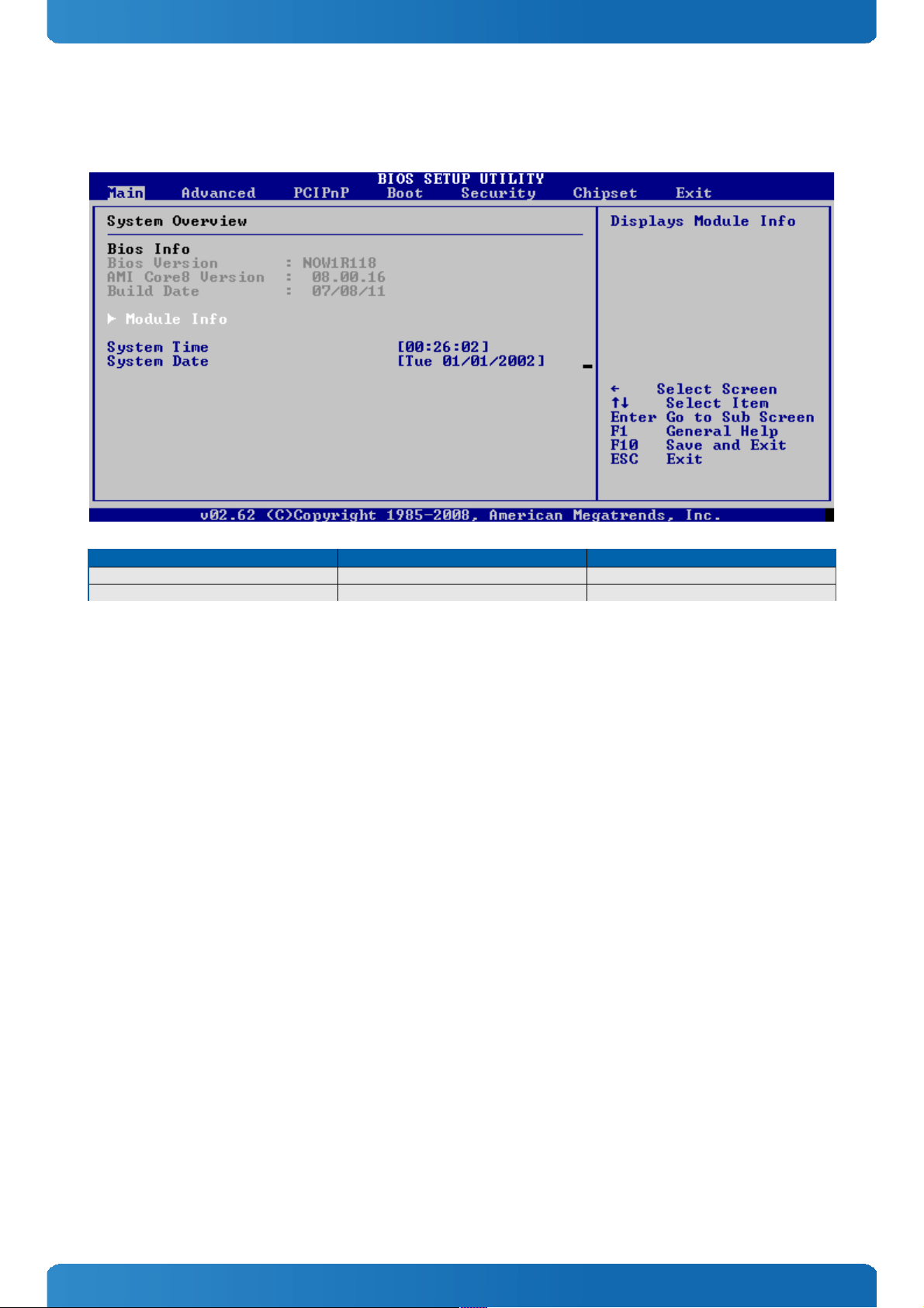
COMe-mSP1 / BIOS Operation
6.4 BIOS Setup
6.4.1 Main Menu
Feature Option Description
System Time [hh:mm:ss] <Tab>, <Shift-Tab>, or <Enter> selects field
System Date [mm-dd-yyyy] <Tab>, <Shift-Tab>, or <Enter> selects field
63
Page 64

COMe-mSP1 / BIOS Operation
6.4.2 Module Info
Module Component Steppings
64
Page 65

COMe-mSP1 / BIOS Operation
Module Software Revisions
Memory Module Information
65
Page 66

COMe-mSP1 / BIOS Operation
Slot 1
Current Memory Configuration SLOT1 shows information of onboard system memory stored
in SPD. The SPD EEPROM is supported with CE 4.x.x (PCB L140) or newer.
Current LVDS Configuration
66
Page 67

COMe-mSP1 / BIOS Operation
6.4.3 Advanced Menu
67
Page 68

COMe-mSP1 / BIOS Operation
CPU Configuration
Feature Option Description
Max CPUID Value Limit
Disabled
Enabled
Disabled for WindowsXP
Intel® Virtualization Tech
Enabled
Disabled
When enabled, a VMM can utilize the additional HW
Caps, provided by Intel® Virtualization Tech. Note: A
full reset is required to change the setting.
CPU TM Functionality
Enabled
Disabled
Enables or disables both TM1 and TM2 simultaneously.
CPU Performance Low
Middle
High
Sets the CPU ratio for Z510/Z530 CPU
Low: 600MHz / 800MHz
Middle: 800MHz / 1200MHz
High: 1100MHz / 1600MHz
Note: Disable Speedstep to use fixed CPU speed to the
selected performance state. With BIOS NOW1R113 or
newer EIST is automatically disabled if set to low or
middle.
Execute-Disable Bit Capability
Enabled
Disabled
When disabled, force the XD feature flag to always
return 0
Hyper Threading Technology
Enabled
Disabled
Enable/Disable Intel® Hyper Threading Technology
DTS-based Thermal Management
Enabled
Disabled
Enable/Disable Thermal Management utilizing the CPU’s
Digital Thermal Sensor
Intel® SpeedStep™
Enabled
Disabled
Enables and Disables the SpeedStep power management
feature
Intel® C-State Technology
Enabled
Disabled
Enables and Disables the C - States. If enabled, the CPU
is set to C2 - C4 state in idle mode
C6 state
Enabled
Disabled
Enables and Disables the C6 - State.
Enhanced C-State Modes
Enabled
Disabled
CPU idle is set to enhanced C-states, when enabled
68
Page 69

COMe-mSP1 / BIOS Operation
IDE Configuration
Feature Option Description
IDE Controller
Enabled
Disabled
Enables or disables the IDE interface of US15W SCH.
This concerns the onboard SSD and PATA2SATA brdige.
Hard Disk Write Protect
Disabled
Enabled
Disables/enables device write protection. It will be
effective only if device is accessed through BIOS
functions.
IDE Detect Time Out (Sec.)
[0-35] 35
Selects the time out value for the detection of ATA/
ATAPI devices
69
Page 70

COMe-mSP1 / BIOS Operation
IDE Device Submenu
Feature Option Description
Type Not Installed
Auto
CD/DVD
ARMD
Selects the type of the IDE Devices connected to the
system
LBA/Large Mode Disabled
Auto
Disables the LBA mode or enables it, when a device
supports it
Block (Multi-Sector Transfer) Disabled
Auto
Disabled: The data transfer from and to the device
occurs one sector ata atime
Auto: The data transfer from and to the device occurs
multiple sectors at a time if the device supports ist
PIO Mode
Auto
0
1
2
3
4
(Auto) Configures the PIO Mode
DMA Mode
Auto
SWDMAn
MWDMAn
UDMAn
SWDMA: Single Word DMA
MWDMA: Multi Word DMA
UDMA: Ultra DMA
S.M.A.R.T.
Auto
Enabled
Disabled
Disables, Enables or automatically enables the
S.M.A.R.T feature (Self-Monitoring, Analysis and
Reporting Technology)
32Bit Data Transfer
Enabled
Disabled
Disables and Enables the 32Bit Data Transfer Mode
70
Page 71

COMe-mSP1 / BIOS Operation
SDIO Configuration
Feature Option Description
Select SDIO or GPIO
SD Card
GPIO
The SD card interface is shared with module GPIO
signals. To use GPIO with this module it is necessary to
set this switch to GPIO.
Data Access Mode
Auto
DMA
PIO
Auto: Access SD device in DMA mode if controller
supports it, otherwise in PIO mode.
DMA: Access SD device in DMA mode.
PIO: Access SD device in PIO mode.
SDIO Clock
Auto
24 MHz
Limit SDIO Clock to 24MHz. Auto setting enables 48MHz
clock if supported by the SDIO device.
The SDIO/GPIO switch is only supported on hardware revisions CE 4.x.x or newer. Modules
with revision CE 1.x.x must be reworked to enable GPIO functionality.
71
Page 72

COMe-mSP1 / BIOS Operation
LPC I/O Controller Configuration
Feature Option Description
Serial Port1 Address Disabled
3F8/IRQ4
2F8/IRQ3
3E8/IRQ4
2E8/IRQ3
Selects the Address of COM Port 1
Serial Port2 Address Disabled
3F8/IRQ4
2F8/IRQ3
3E8/IRQ4
2E8/IRQ3
Selects the Address of COM Port 2
Serial Port2 Mode
Normal
IrDA
ASKIR
Selects the mode for serial Port 2
Parallel Port Address Disabled
378
278
3BC
Selects the Address of the LPT Port
Parallel Port Mode
Normal
Bi-Directional
ECP
EPP
ECP+SPP
Allows BIOS to Select Parallel Port Mode. (Only visible
when Parallel Port enabled.)
Parallel Port IRQ IRQ5
IRQ7
Allows BIOS to Select Parallel Port IRQ. (Only visible
when Parallel Port enabled.)
72
Page 73

COMe-mSP1 / BIOS Operation
ACPI Configuration
Feature Option Description
ACPI Version
ACPI v.3.0
ACPI v.2.0
Selects the ACPI version
ACPI APIC support
Enabled
Disabled
Include ACPI APIC table pointer to RSDT pointer list.
Repost Video on S3 Resume
No
Yes
If yes, Videobios is reinitialized after S3 Resume
AMI OEMB Table
Enabled
Disabled
Includes the AMI OEMB table pointer. The OEMB table is
used to fill in POST data in AML code during ACPI OS
operations. This option should only be disabled if ACPI
1.0 is used
Headless Mode
Disabled
Enabled
Enables / Disables headless mode through ACPI
73
Page 74

COMe-mSP1 / BIOS Operation
ACPI Cooling Options
Feature Option Description
Passive Trip Point
Disabled
40°C
45°C
50°C
…
110°C
This value controls the temperature of the ACPI Passive
Trip Point - the point in which the OS will begin
throttling the CPU.
Passive TC1 value
1
2
3
…
16
This value sets the TC1 value for the ACPI Passive
Cooling Formula. (Only visible when Passive Trip Point is
enabled.)
Passive TC2 value 1
2
…
5
…
16
This value sets the TC2 value for the ACPI Passive
Cooling Formula. (Only visible when Passive Trip Point is
enabled.)
Passive TSP value 2
4
…
10
…
30
This item sets the TSP value for the ACPI Passive Cooling
Formula. It represents in tenths of a second how often
the OS will read the temperature when Passive Cooling
is Enabled.
Critical Trip Point Disabled
40°C
45°C
50°C
…
110°C
This value controls the temperature of the ACPI Critical
Trip Point - the point in which the OS will shut off the
system.
74
Page 75

COMe-mSP1 / BIOS Operation
Passive Cooling
The ACPI OS assesses the optimum CPU performance change necessary to lower the temperature using the following
equation
?P[%] = TC1(Tn-Tn-1) + TC2(Tn-Tt)
?P is the performance delta, Tt is the target temperature = passive cooling trip point. The two coeff icients TC1 and TC2 and
the sampling period TSP are hardware dependent constants the end user must supply. It’s up to the end user to set the
cooling preference of the system by setting the appropriate trip points in the BIOS setup.
See chapter 12 of the ACPI specification (www.acpi.info) for more details
75
Page 76

COMe-mSP1 / BIOS Operation
Miscellaneous Settings
Feature Option Description
Spread Spectrum
Disabled
LVDS
Core
Both
Enables or Disables spread spectrum for the selected
Clocks.
LVDS: Enables LVDS Spread Spectrum
Core: Enables CPU, PCIe, Chipset Spread Spectrum
A20 line controlled by
Auto Detection
Legacy Keyb Ctrl.
Port 92h emul
This setting allows choosing how address line A20 is
controlled for legacy systems. If Keyb. controller is
chosen an active KBC is needed
Keyboard Crisis Recovery Disabled
Enabled
Enables/Disables Keyboard Crisis Recovery function by
USB keyboard
Smbios Smi Support
Enabled
Disabled
SMBIOS SMI Wrapper support for PnP Functions 50h54h
76
Page 77

COMe-mSP1 / BIOS Operation
I2C Buses
Feature Option Description
JIDA I2C Bus Speed
Very high
High
Medium
Slow
Very slow
Ultra Slow
Select speed for JIDA/external I2C bus. See speed table
in chapter Fast I2C.
Multi Master support
Enabled
Disabled
Enables / disables I2C multi master support
Clock Stretching support
Enabled
Disabled
Enables / disables I2C clock stretching support
Slow Device support
Enabled
Disabled
Enables / disables I2C clock stretching support
SMBus SPeed Extra high
Very high
High
Medium
Slow
Very Slow
Select speed for external SMBus. See speed table in
chapter Fast I2C.
JILI I2C Bus Speed Very high
High
Medium
Slow
Very Slow
Select speed for external JILI I2C bus. See speed table
in chapter Fast I2C.
Multi Master support
Enabled
Disabled
Enables / disables I2C multi master support
Clock Stretching support
Enabled
Disabled
Enables / disables I2C clock stretching support
Slow Device support
Enabled
Disabled
Enables / disables I2C clock stretching support
77
Page 78

COMe-mSP1 / BIOS Operation
Watchdog
Feature Option Description
Mode Reset
Disabled
Selects the mode of the watchdog
Timeout 1s
5s
10s
30s
1:00m
5:00m
10:00m
Set the timout for Watchdog
78
Page 79

COMe-mSP1 / BIOS Operation
MARS Interface Configuration
Feature Option Description
MARS
Disabled
Auto
SMB Charger
SMB Manager
Enables the MARS function
79
Page 80

COMe-mSP1 / BIOS Operation
Ethernet Configuration
Feature Option Description
Onboard Gigabit Ethernet Disabled
Enabled
Disables / Enables the onboard Ethernet interface
PXE ROM
Disabled
Enabled
Disables / Enables the PXE Boot ROM
80
Page 81

COMe-mSP1 / BIOS Operation
PCIExpress Configuration
Feature Option Description
PCIe Ports
Both
Disabled
Port 0
Port 1
Disables or enables according PCI Express lanes.
Onboard Gigabit Ethernet is connected to Port 1.
Port 0/1: enables specific PCI Express Lane
Both: Both PCI Express lanes from US15W SCH are
enabled
Disabled: US15W SCH PCI Express is completely disabled
PCIE Base Spec Compliance Disabled
Enabled
Allows to choose between strict PCIE base specif ication
compliance and power saving mode.
Warning: Disabling PCIE compliance might influence the
PCIE lane throughput.
SDVO PCIE Base Spec Compliance
Disabled
Enabled
Allows to choose between strict PCIE base specif ication
compliance and power saving mode.
Warning: Disabling SDVO compliance might influence
the PCIE lane throughput.
Active State Power Management
Disabled
Enabled
Enables/Disables PCI Express L0 and L1 link power
states.
81
Page 82

COMe-mSP1 / BIOS Operation
Trusted Computing
Feature Option Description
TCG/TPM SUPPORT
No
Yes
Enable/Disable TPM TCG (TPM 1.1/1.2) support in BIOS
82
Page 83

COMe-mSP1 / BIOS Operation
USB Configuration
Feature Option Description
Legacy USB Support Disabled
Enabled
Enables / disables support for legacy USB.
USB 2.0 Controller Mode FullSpeed
HiSpeed
Configures the USB 2.0 controller in HiSpeed
(480Mbps) or FullSpeed (12Mbps)
BIOS EHCI Hand-Off Disabled
Enabled
This is a workaround for an OS without EHCI hand-off
support. The EHCI ownership change should claim by
the EHCI driver
83
Page 84

COMe-mSP1 / BIOS Operation
USB Mass Storage Device Configuration
Feature Option Description
USB Mass Storage Reset Delay 10 Sec
20 Sec
30 Sec
40 Sec
Number of seconds POST waits for the USB mass storage
device after start unit command.
Emulation Type
Auto
Floppy
Forced FDD
Hard Disk
CDROM
If Auto USB devices with less than 20MB will be
emulated as floppy and remaining as hard drive. Forced
FDD option can be used to force a HDD formatted drive
to boot as FDD (Ex. ZIP drive).
84
Page 85

COMe-mSP1 / BIOS Operation
Hardware Health Configuration
Feature Option Description
Module HWM:
H/W Health Function
Disabled
Enabled
Enables the onboard Hardware Health Monitoring
Device
CPU Temperature: CPU ACPI temperature
Module Temperature: Internal temperature of HWM
Chipset Sensor #1 / Chipset Sensor #2: Internal
thermal sensors of US15W SCH to cause main memory
throttling and display refresh throttling.
See JIDA32/K-Station resource list for more details
Baseboard HWM:
H/W Health Function
Disabled
Enabled
Enables the Hardware Health Monitoring suppor t for
external LPC I/O Winbond 83627
Fan Speed Selector 1
2
4
…
128
Select the FAN Speed Divisor according to nominal
revolutions per minute of used FAN:
Divisor 1: 8800 rpm, Divisor 2: 4400 rpm
Divisor 4: 2200 rpm, Divisor 8: 1100 rpm
Divisor 16: 550 rpm, Divisor 32: 275 rpm
Divisor 64: 137 rpm, Divisor 128: 68 rpm
Fan Ticks per Rev 1
2
4
8
Number of Ticks per Revolution
85
Page 86

COMe-mSP1 / BIOS Operation
6.4.4 Advanced PCI/PnP Settings
Feature Option Description
Clear NVRAM
No
Yes
Clear NVRAM once during next system boot.
PCI Latency Timer 32
64
…
248
Value in units of PCI clocks for PCI device latency
register
PCI IDE BusMaster Disabled
Enabled
Disables and enables PCI IDE Busmaster
IRQ3 … IRQ15
Available
Reserved
Available: IRQ useable by PCI/PnP devices
Reserved: IRQ is reserved for ISA devices
Reserved Memory Size
Disabled
16k
32k
64k
Size of memory block to reserve for legacy ISA devices
86
Page 87

COMe-mSP1 / BIOS Operation
6.4.5 Boot
87
Page 88

COMe-mSP1 / BIOS Operation
Boot Setting Configuration
Feature Option Description
Dark Boot
Disabled
Enabled
Disabled: Shows normal POST messages
Enabled: Shows OEM Logo during boot up
AddOn ROM Display Mode
Force BIOS
Keep Current
Set Display Mode for Option ROM
Bootup Num-Lock
On
Off
Select Power-On state for Num-Lock
PS/2 Mouse Support
Auto
Disabled
Enabled
Disables and enables or auto selects PS/2 Mouse
Support
Wait For 'F1' If Error
Disabled
Enabled
Wait for F1 key to be pressed, if error
“Press DEL” Message Display
Enabled
Disabled
Enabled allows the BIOS to display the message Press
DEL to run Setup after memor y initialization. Disabled
suppresses this message
Boot USB HDD first
Disabled
Enabled
If enabled, boots new attached USB HDD always first
Interrupt 19 Capture
Disabled
Enabled
Allows option ROMs to trap INT19h if enabled
88
Page 89

COMe-mSP1 / BIOS Operation
USB Bootable Port Configuration
Feature Option Description
Port 0 - 7 Disabled
Enabled
Enables/Disables a specific port to be bootable
89
Page 90

COMe-mSP1 / BIOS Operation
6.4.6 Security
Feature Option Description
Change Supervisor Password
Type in
Change User Password
Type in
Boot Sector Virus Protection
Disabled
Enabled
Enables or disables boot sector virus protection.
90
Page 91

COMe-mSP1 / BIOS Operation
6.4.7 Advanced Chipset Settings
91
Page 92

COMe-mSP1 / BIOS Operation
Graphic Controller Configuration
Feature Option Description
Primary Graphic Adapter
PCIe/Onboard
Onboard
Selects which graphics controller is used as primary
boot device (boot sequence)
Onboard Graphic Mode Disabled
Enabled, 1MB
Enabled, 4MB
Enabled, 8MB
Selects the amount of pre-allocated system memory
used by the onboard graphics controller
Aperture Size
256MB
128MB
Configures the size of the aper ture space.
Needs IEGD driver.
92
Page 93

COMe-mSP1 / BIOS Operation
Display Control
Feature Option Description
Boot Display Device
Auto
LVDS
SDVO-CRT
SDVO-DVI/HDMI
Select the Boot Display Device.
Note: SDVO is not supported on HW Rev CE 1.x.x (PCB
L130)
93
Page 94

COMe-mSP1 / BIOS Operation
Internal LVDS Configuration
Feature Option Description
Flat Panel Mode
Auto
Fixed Mode
PAID
FPID
Selects the Mode for the flat panel detection
Auto Fallback Disabled
Fixed Mode
Selects what happens, when there is no EEPROM
detected (only when FPM: Auto)
Flat Panel Type VGA 640×480
SVGA 800×600
…
WXGA 1280×800
Selects the resolution of the LVDS display (only in FMP:
Fixed Mode)
PAID/FPID [X] Selects the number of the PAID/FPID
Color Depth
18bit
24bit
Selects the Color Depth of the connected LVDS display
(only in FPM: Fixed Mode)
Local Flat Panel Scaling Centered
Stretched
Disabled
Selects the Scaling Options for the LVDS panel (only in
FPM: Fixed Mode)
LVDS DVI ID → 5
7
Select the type of used LVDStoDVI converter
5 = 1x18bit Adapter, 7 = 1x24bit Adapter
Backlight Control Type None/External
I2C
PWM
Selects the mode for Backlight Control
Backlight Brightness [0…255] Selects the default setting for Backlight Brightness
94
Page 95

COMe-mSP1 / BIOS Operation
System Controller Hub Configuration
Feature Option Description
USB UHCI Controller Disabled
2 USB Ports
4 USB Ports
…
8 USB Ports
Enables / Disables USB ports
USB EHCI Controller
Enabled
Disabled
Controls EHCI (USB 2.0) functionality for all the UHCI
ports set to active state
USB Client Controller Enabled
Disabled
This enables the USB client functionality on COM
Express USB Port #7
Audio Controller
HDAudio
Disabled
Enables / Disables the HDA audio controller
Serial IRQ Mode
Continuous
Quiet
Defines the serial IRQ mode (Quiet = the chipset
communicates only if an IRQ is triggered) for the LPC
interface
95
Page 96

COMe-mSP1 / BIOS Operation
6.4.8 Exit Menu
Feature Description
Save To RTC/EEPROM and Exit Saving system setup to RTC and EEPROM and exit setup. F10 key can be used for this
operation
Save As Custom Defaults To RTC/Flash and Exit Saving system setup as custom defaults to RTC and Flash and exit setup. F11 key can
be used for this operation. Refer to Flash Backup Feature for more details
Discard Changes and Exit Exit system setup without saving any changes. ESC key can be used for this operation
Discard Changes Discards changes done so far to any of the setup questions. F7 key can be used for
this operation
Load Manufacturing Defaults Load manufacturing default values for all the setup questions. F9 key can be used for
this operation
Load Custom Defaults Load custom default values for all the setup questions.
.
.
.
.
.
.
.
.
..
.
.
.
.
.
.
.
.
.
.
.
.
.
.
.
.
.
.
.
.
.
.
.
96
Page 97

COMe-mSP1 / BIOS Operation
.
.
.
.
.
.
.
.
.
.
.
.
.
.
Corporate Offices
Europe, Middle East & Africa
Oskar-von-Miller-Str. 1
85386 Eching/Munich
Germany
Tel.: +49 (0)8165/ 77 777
Fax: +49 (0)8165/ 77 219
info@kontron.com
North America
14118 Stowe Drive
Poway, CA 92064-7147
USA
Tel.: +1 888 294 4558
Fax: +1 858 677 0898
info@us.kontron.com
Asia Pacific
17 Building,Block #1,ABP.
188 Southern West 4th Ring
Beijing 100070, P.R.China
Tel.: + 86 10 63751188
Fax: + 86 10 83682438
info@kontron.cn
97
 Loading...