

Page 1
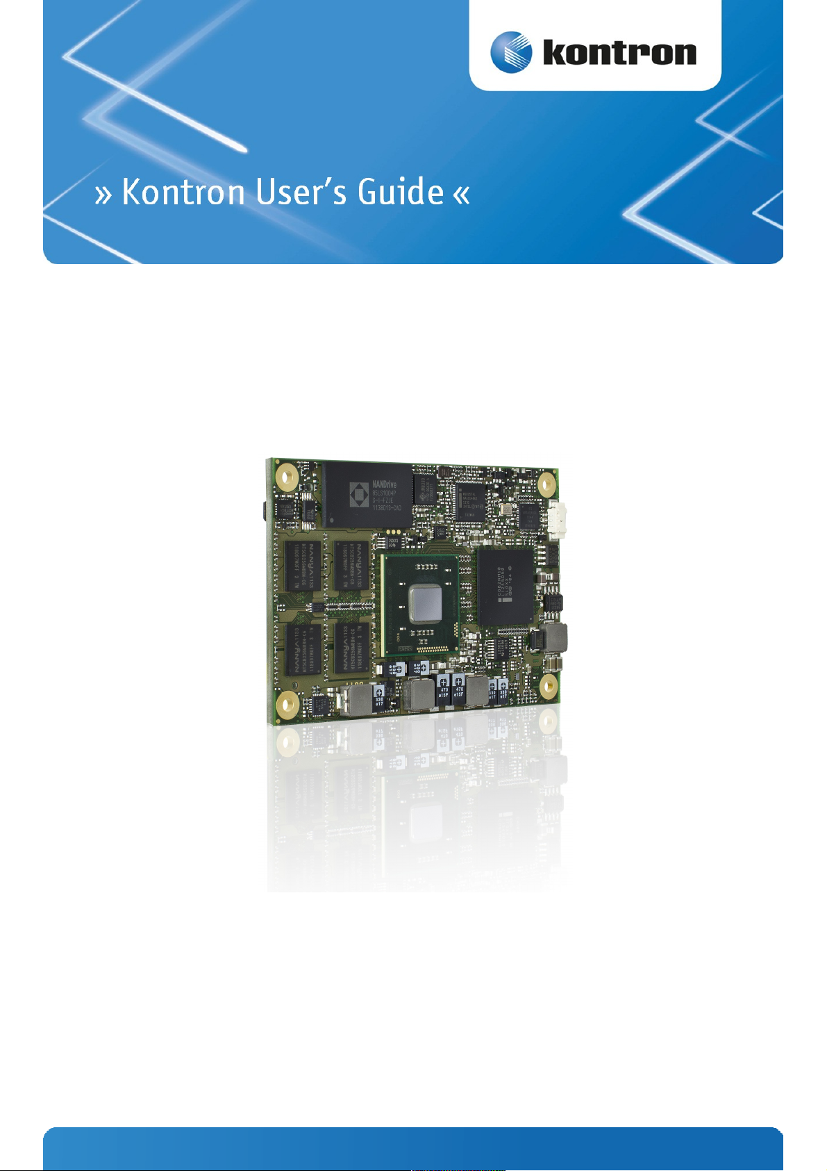
COMe-mCT10
Document Revision 130
www.kontron.com
Page 2

Page 3

» Table of Contents «
1 User Information..................................................................................5
1.1 About This Document.................................................................................................................... 5
1.2 Copyright Notice.......................................................................................................................... 5
1.3 Trademarks................................................................................................................................. 5
1.4 Standards................................................................................................................................... 5
1.5 Warranty.................................................................................................................................... 6
1.6 Technical Support......................................................................................................................... 6
2 Introduction........................................................................................7
2.1 Product Description...................................................................................................................... 7
2.2 Naming clarification..................................................................................................................... 7
2.3 Understanding COM Express® Functionality.......................................................................................7
2.4 COM Express® Documentation......................................................................................................... 8
2.5 COM Express® Benefits.................................................................................................................. 8
3 Product Specification............................................................................9
3.1 Module definition......................................................................................................................... 9
3.2 Functional Specification............................................................................................................... 11
3.3 Block Diagram............................................................................................................................ 15
3.4 Accessories............................................................................................................................... 16
3.5 Electrical Specification................................................................................................................ 17
3.5.1 Supply Voltage........................................................................................................................... 17
3.5.2 Power Supply Rise Time................................................................................................................17
3.5.3 Supply Voltage Ripple.................................................................................................................. 17
3.5.4 Power Consumption..................................................................................................................... 17
3.5.5 ATX Mode.................................................................................................................................. 18
3.5.6 Single Supply Mode..................................................................................................................... 18
3.6 Power Control............................................................................................................................ 19
3.7 Environmental Specification......................................................................................................... 20
3.7.1 Temperature Specification............................................................................................................ 20
3.7.2 Humidity................................................................................................................................... 20
3.8 Standards and Certifications.........................................................................................................21
3.9 MTBF........................................................................................................................................ 23
3.10 Mechanical Specification.............................................................................................................. 24
3.11 Thermal Management, Heatspreader and Cooling Solutions.................................................................25
3.12 Onboard Fan Connector................................................................................................................ 26
4 Features and Interfaces.......................................................................27
4.1 Onboard SSD.............................................................................................................................. 27
4.2 S5 Eco Mode.............................................................................................................................. 28
4.3 LPC.......................................................................................................................................... 29
4.4 Serial Peripheral Interface (SPI)....................................................................................................30
www.kontron.com
Page 4

COMe-mCT10 /
4.5 SPI boot.................................................................................................................................... 30
4.6 M.A.R.S.................................................................................................................................... 32
4.7 UART........................................................................................................................................ 33
4.8 Fast I2C.................................................................................................................................... 34
4.9 GPIO - General Purpose Input and Output.........................................................................................35
4.10 Dual Staged Watchdog Timer......................................................................................................... 36
4.11 Intel® Fast Flash Standby™ / Rapid Start Technology™.......................................................................37
4.12 Speedstep Technology................................................................................................................. 39
4.13 C-States.................................................................................................................................... 40
4.14 Hyper Threading......................................................................................................................... 41
4.15 Graphics Features....................................................................................................................... 42
4.16 Hardware Configuration............................................................................................................... 42
4.17 Graphics VBIOS and Driver............................................................................................................ 42
4.18 ACPI Suspend Modes and Resume Events..........................................................................................43
4.19 USB......................................................................................................................................... 44
5 System Resources...............................................................................45
5.1 Interrupt Request (IRQ) Lines........................................................................................................ 45
5.2 Memory Area............................................................................................................................. 45
5.3 I/O Address Map......................................................................................................................... 46
5.4 Peripheral Component Interconnect (PCI) Devices............................................................................. 46
5.5 I2C Bus..................................................................................................................................... 47
5.6 JILI I2C Bus............................................................................................................................... 47
5.7 System Management (SM) Bus....................................................................................................... 47
6 Pinout List.........................................................................................48
6.1 General Signal Description............................................................................................................ 48
6.2 Connector X1A Row A................................................................................................................... 49
6.3 Connector X1A Row B................................................................................................................... 51
7 BIOS Operation...................................................................................53
7.1 Determining the BIOS Version....................................................................................................... 53
7.2 BIOS Update.............................................................................................................................. 53
7.3 Setup Guide............................................................................................................................... 55
7.4 POST Codes................................................................................................................................ 55
7.4.1 Start AMI® Aptio Setup Utility....................................................................................................... 55
7.5 BIOS Setup................................................................................................................................ 57
7.5.1 Main Menu................................................................................................................................. 57
7.5.2 Advanced.................................................................................................................................. 59
7.5.3 Chipset..................................................................................................................................... 89
7.5.4 Boot........................................................................................................................................ 96
7.5.5 Security.................................................................................................................................... 97
7.5.6 Save & Exit................................................................................................................................ 99
4
Page 5

COMe-mCT10 / User Information
1 User Information
1.1 About This Document
This document provides information about products from Kontron Europe GmbH and/or its subsidiaries. No warranty of
suitability, purpose, or fitness is implied. While every attempt has been made to ensure that the information in this
document is accurate, the information contained within is supplied “as-is” and is subject to change without notice.
For the circuits, descriptions and tables indicated, Kontron assumes no responsibility as far as patents or other rights of
third parties are concerned.
1.2 Copyright Notice
Copyright © 2003-2014 Kontron Europe GmbH
All rights reserved. No part of this document may be reproduced, transmitted, transcribed, stored in a retrieval system, or
translated into any language or computer language, in any form or by any means (electronic, mechanical, photocopying,
recording, or otherwise), without the express written permission of Kontron Europe GmbH.
DIMM-PC®, PISA®, ETX®, ETXexpress®, microETXexpress®, X-board®, DIMM-IO® and DIMM-BUS® are trademarks or
registered trademarks of Kontron Europe GmbH. Kontron is trademark or registered trademark of Kontron AG.
1.3 Trademarks
The following lists the trademarks of components used in this board.
» IBM, XT, AT, PS/2 and Personal System/2 are trademarks of International Business Machines Corp.
» Microsoft is a registered trademark of Microsoft Corp.
» Intel is a registered trademark of Intel Corp.
» All other products and trademarks mentioned in this manual are trademarks of their respective owners.
1.4 Standards
Kontron Europe GmbH is certified to ISO 9000 standards.
5
Page 6

COMe-mCT10 / User Information
1.5 Warranty
For this Kontron Europe GmbH product warranty for defects in material and workmanship exists as long as the warranty
period, beginning with the date of shipment, lasts. During the warranty period, Kontron Europe GmbH will decide on its
discretion if defective products are to be repaired or replaced.
Within the warranty period, the repair of products is free of charge as long as warranty conditions are observed.
Warranty does not apply for defects arising/resulting from improper or inadequate maintenance or handling by the buyer,
unauthorized modification or misuse, as well as the operation outside of the product´s environmental specifications and
improper installation and maintenance.
Kontron Europe GmbH will not be responsible for any defects or damages to other products not supplied by Kontron
Europe GmbH that are caused by a faulty Kontron Europe GmbH product.
1.6 Technical Support
Technicians and engineers from Kontron Europe GmbH and/or its subsidiaries are available for technical support. We are
committed to make our product easy to use and will help you use our products in your systems.
Please consult our Website at http://www.kontron.com/support for the latest product documentation, utilities, drivers
and support contacts. Consult our customer section http://emdcustomersection.kontron.com for the latest BIOS
downloads, Product Change Notifications, Board Support Packages, DemoImages, 3D drawings and additional tools and
software. In any case you can always contact your board supplier for technical support.
6
Page 7

COMe-mCT10 / Introduction
2 Introduction
2.1 Product Description
The first credit card sized (55mm x 84 mm) COM Express® mini COM based on Intel® 32nm Dual Core technology. Three
performance versions are availabe from 2x 1.6 GHz up to 2x 1.86 GHz. With onboard memory and optional flash as well as
divesified graphics interfaces, the Kontron COMe-mCT10 series is optimized for the Industrial Automation, Infotainment
and Medical markets to deliver outstanding graphics performance.
2.2 Naming clarification
COM Express® defines a Computer-On-Module, or COM, with all components necessary for a bootable host computer,
packaged as a super component.
» COMe-bXX# modules are Kontron's COM Express® modules in basic form factor (125mm x 95mm)
» COMe-cXX# modules are Kontron's COM Express® modules in compact form factor (95mm x 95mm)
» COMe-mXX# modules are Kontron's COM Express® modules in mini form factor (55mm x 84mm)
The product names for Kontron COM Express® Computer-on-Modules consist of a short form of the industry standard
(COMe-), the form factor (b=basic, c=compact, m=mini), the capital letters for the CPU and Chipset Codenames (XX) and
the pin-out type (#) followed by the CPU Name.
2.3 Understanding COM Express® Functionality
All Kontron COM Express® basic and compact modules contain two 220pin connectors; each of it has two rows called Row
A & B on primary connector and Row C & D on secondary connector. COM Express® Computer-on-modules feature the
following maximum amount of interfaces according to the PICMG module Pin-out type:
Feature Pin-Out Type 1 Pin-Out Type 10 Pin-Out Type 2 Pin-Out Type 6
HD Audio
1x 1x 1x 1x
Gbit Ethernet
1x 1x 1x 1x
Serial ATA
4x 4x 4x 4x
Parallel ATA
- - 1x -
PCI
- - 1x -
PCI Express x1
6x 6x 6x 8x
PCI Express x16 (PEG)
- - 1x 1x
USB Client
1x 1x - -
USB 2.0
8x 8x 8x 8x
USB 3.0
- 2x - 4x
VGA
1x - 1x 1x
LVDS
Dual Channel Single Channel Dual Channel Dual Channel
DP++ (SDVO/DP/HDMI/DVI)
1x optional 1x 3x shared with PEG 3x
LPC
1x 1x 1x 1x
External SMB
1x 1x 1x 1x
External I2C
1x 1x 1x 1x
GPIO
8x 8x 8x 8x
SDIO shared w/GPIO
1x optional 1x optional - 1x optional
UART (2-wire COM)
- 2x - 2x
FAN PWM out
- 1x - 1x
7
Page 8
COMe-mCT10 / Introduction
2.4 COM Express® Documentation
This product manual serves as one of three principal references for a COM Express® design. It documents the
specifications and features of COMe-mCT10. Additional references are available at your Kontron Support or at PICMG®:
» The COM Express® Specification defines the COM Express® module form factor, pin-out, and signals. This document
is available at the PICMG® website by filling out the order form.
» The COM Express® Design Guide by PICMG® serves as a general guide for baseboard design, with a focus on
maximum flexibility to accommodate a wide range of COM Express® modules.
Some of the information contained within this product manual applies only to certain
product revisions (CE: xxx). If certain information applies to specific product revisions (CE:
xxx) it will be stated. Please check the product revision of your module to see if this
information is applicable.
2.5 COM Express® Benefits
COM Express® modules are very compact, highly integrated computers. All Kontron COM Express® modules feature a
standardized form factor and a standardized connector layout which carry a specified set of signals. Each COM is based on
the COM Express® specification. This standardization allows designers to create a single-system baseboard that can
accept present and future COM Express® modules.
The baseboard designer can optimize exactly how each of these functions implements physically. Designers can place
connectors precisely where needed for the application on a baseboard designed to optimally fit a system’s packaging.
A single baseboard design can use a range of COM Express® modules with different sizes and pin-outs. This flexibility can
differentiate products at various price/performance points, or when designing future proof systems that have a built-in
upgrade path. The modularity of a COM Express® solution also ensures against obsolescence when computer technology
evolves. A properly designed COM Express® baseboard can work with several successive generations of COM Express®
modules.
A COM Express® baseboard design has many advantages of a customized computer-board design and, additionally,
delivers better obsolescence protection, heavily reduced engineering effort, and faster time to market.
8
Page 9
COMe-mCT10 / Product Specification
3 Product Specification
3.1 Module definition
The COM Express® mini sized Computer-on-Module COMe-mCT10 (NUP1) follows pin-out Type 10 and is compatible to
PICMG specification COM.0 Rev 2.0. The COMe-mCT10, based on Intel's Cedar Trail platform, is available in different
variants to cover the demand of different performance, price and power:
Commercial grade modules (0°C to 60°C operating)
Part Number Product Name Processor DDR3 Flash UART TPM onboard FAN
34005-4032-19-7 COMe-mCT10 D2550 4/32GB Cedarview-D Intel® Atom™ D2550 4GB 32GB MLC 2 YES YES
34005-2040-19-6 COMe-mCT10 D2550 2GB/4GB Cedarview-D Intel® Atom™ D2550 2GB 4GB SLC - - YES
34005-1040-19-2 COMe-mCT10 N2800 1GB/4GB Cedarview-M Intel® Atom™ N2800 1GB 4GB SLC - - YES
34005-1040-16-2 COMe-mCT10 N2600 1GB/4GB Cedarview-M Intel® Atom™ N2600 1GB 4GB SLC - - -
34005-2040-16-2 COMe-mCT10 N2600 2GB/4GB Cedarview-M Intel® Atom™ N2600 2GB 4GB SLC 2 - -
34005-2000-19-6 COMe-mCT10 D2550 2GB Cedarview-D Intel® Atom™ D2550 2GB - 2 - YES
34005-2000-19-2 COMe-mCT10 N2800 2GB Cedar view-M Intel® Atom™ N2800 2GB - 2 - YES
34005-2000-16-2 COMe-mCT10 N2600 2GB Cedar view-M Intel® Atom™ N2600 2GB - 2 - -
34005-1000-19-6 COMe-mCT10 D2550 1GB Cedarview-D Intel® Atom™ D2550 1GB - - - YES
34005-1000-19-2 COMe-mCT10 N2800 1GB Cedar view-M Intel® Atom™ N2800 1GB - - - YES
34005-1000-16-2 COMe-mCT10 N2600 1GB Cedar view-M Intel® Atom™ N2600 1GB - - - -
Extended temperature grade modules (E1, -25°C to 75°C operating)
Part Number Product Name Processor DDR3 Flash UART TPM onboard FAN
34005-2040-19-6EXT COMe-mCT10 D2550 2/4GB E1 Cedarview-D Intel® Atom™ D2550 2GB 4GB SLC - - YES
34005-1000-19-2EXT COMe-mCT10 N2800 1GB E1 Cedarview-M Intel® Atom™ N2800 1GB - - - YES
34005-2000-16-2EXT COMe-mCT10 N2600 2GB E1 Cedarview-M Intel® Atom™ N2600 2GB - 2 - -
34005-1000-16-2EXT COMe-mCT10 N2600 1GB E1 Cedarview-M Intel® Atom™ N2600 1GB - - - -
Industrial temperature grade modules (XT, -40°C to 85°C operating)
Modules for E2 temperature range are available project based only, please contact your local sales or support for further
details.
Part Number Product Name Processor DDR3 Flash UART TPM onboard FAN
34005-MMFF-CC-X COMe-mCT10 All 1/2GB E2 optional optional n/a YES
The COMe-mCT10 is available for industrial temperature range. General capability was tested for following options:
» CPU: all
» Memory down: 1GB or 2GB industrial temperature grade
» Onboard flash: industrial grade MLC or SLC
» Options: 2x UART, FAN Connector
» Not available: TPM option
9
Page 10

COMe-mCT10 / Product Specification
Memory and onboard Flash configurations 34005-MMFF-xx-x:
» MM = 10: 1024MB DDR3 Memory (8x1Gbit / 128Mx8)
» MM = 20: 2048MB DDR3 Memory (8x2Gbit / 256Mx8)
» FF = 00: without SATA SSD
» FF = 20: 2GB onboard SATA SSD
» FF = 40: 4GB onboard SATA SSD
» FF = 80: 8GB onboard SATA SSD
» FF = 16: 16GB onboard SATA SSD
» FF = 32: 32GB onboard SATA SSD
» FF = 64: 64GB onboard SATA SSD
Optional hardware features:
» TPM (not for E1/E2 variants)
» 2x UART
» 2 to 32GB SLC NANDrive
» 2 to 64GB MLC NANDrive
Optional BIOS features:
» Secure Flash Update
» Secure Boot
» CSM OptOut
Optional hardware and BIOS features are available project based only for variants not listed
above. Please contact your local sales for customized articles.
10
Page 11

COMe-mCT10 / Product Specification
3.2 Functional Specification
Processor
The 32nm Intel® Atom™ D2000/N2000 (Cedarview-M/D) CPU family supports:
» Intel® Hyper-Threading Technology
» Intel® 64
» Enhanced Intel SpeedStep® Technology (N2xxx only)
» Thermal Monitoring Technologies
» Execute Disable Bit
» 2 Display Pipes for dual independent displays
CPU specifications
CPU Intel® Atom™ D2550 Intel® Atom™ N2800 Intel® Atom™ N2600
Cores
2 2 2
Threads
4 4 4
Clock
1866MHz 1866MHz 1600MHz
Memory Speed
DDR3-1066 DDR3-1066 DDR3-800
Max Memory
up to 4GB up to 4GB up to 2GB
Cache
1MB 1MB 1MB
C-States
C0/C1 C0-C6 / C1E-C4E C0-C6 / C1E-C4E
EIST
- YES YES
CPU Thermal Management
TM1 TM1 & TM2 TM1 & TM2
GFX
GMA3650 GMA3650 GMA3600
GFX core frequency
640MHz 640MHz 400MHz
GFX render clock frequency
200MHz 200MHz 200MHz
Display Core Clock
355MHz 267MHz 200MHz
LVDS
1×18/24bit 1×18/24bit 1×18/24bit
LVDS Resolution
up to 1440x900x60 up to 1366x768x60 up to 1366x768x60
eDP Resolution
up to 1920x1080x60 up to 1366x768x60 up to 1366x768x60
DP Resolution
up to 2560x1600x60 up to 1600x1200x60 up to 1600x1200x60
HDMI/DVI Resolution
up to 1920x1200x60 up to 1920x1200x60 up to 1920x1200x60
PAVP
1.1c 1.1c -
HDCP
1.3 1.3 -
Blu-Ray 2.0 Playback
Yes Yes -
TDP
10W 6.5W 3.5W
Memory
Sockets
memory down
Memory Type
DDR3-800 / 1066
Maximum Size
2GB
4GB (512Mx8) of ficially not supported by Intel®
Technology
Single Channel (64bit)
11
Page 12
COMe-mCT10 / Product Specification
Graphics Core
The integrated Intel® GMA 3650 / 3600 based on PowerVR SGX545 core supports:
Graphics Core Render Clock
640MHz @ GMA3650 (D2700/N2800)
400MHz @ GMA3600 (N2600),
Execution Units / Pixel Pipelines
4
Max Graphics Memory
1024MB
GFX Memory Bandwidth (GB/s)
6.4 / 8.5
GFX Memory Technology
DVMT
API (DirectX/OpenGL)
9.0c / 3.0
Shader Model
3.0
Hardware accelerated Video
H.264,MPEG2,VC1, Blu-ray
Independent/Simultaneous Displays
2
Display Port
DP / eDP 1.1
HDCP support
HDCP 1.3a / PAVP 1.1c
Monitor output
CRT max Resolution
-
TV out:
-
LVDS
LVDS Bits/Pixel
1x18 / 1x24
LVDS Bits/Pixel with dithering
-
LVDS max Resolution:
D: 1440x900, M: 1366x768, 112MHz
PWM Backlight Control:
YES
Supported Panel Data:
JILI2/JILI3/EDID/DID
Display Interfaces
Discrete Graphics
-
Digital Display Interface DDI1
DP++
Digital Display Interface DDI2
-
Digital Display Interface DDI3
-
Maximum Resolution on DDI
HDMI: 1920x1200, DP-D: 2560x1600/DP-M: 1600x1200
PCH: Intel® NM10 Express Chipset
The 130nm Intel Platform Controller Hub Tigerpoint supports:
» PCI Express Gen 1.0 Speed
» USB 2.0
» HD Audio
» SATA 3Gb/s
Storage
onboard SSD
2-32GB SLC, 2-64GB MLC (SATA)
SD Card support
- instead of GPIO
IDE Interface
-
Serial-ATA
up to 2x SATA 3Gb/s
SATA AHCI
AHCI 1.0 with NCQ and HotPlug
SATA RAID
-
With onboard SATA drive only 1 external SATA interface (SATA 0) is available
12
Page 13
COMe-mCT10 / Product Specification
Connectivity
USB
8x USB 2.0
USB Client
-
PCI
-
PCI External Masters
-
PCI Express
3x PCIe x1 Gen1
Max PCI Express
4x PCIe x1 without LAN
PCI Express x2/x4 configuration
YES
Ethernet
10/100/1000 Mbit
Ethernet controller
Intel® 82574L (Har twell)
Any PCIe device connecting to Intel@ Atom Processor D2000 and N2000 based platform
must support No_Snoop attribute
Ethernet
The Intel® 82574L (Hartwell) ethernet supports:
» Jumbo Frames
» Time Sync Protocol Indicator
» WOL (Wake On LAN)
» PXE (Preboot eXecution Environment)
Misc Interfaces and Features
Supported BIOS Size/Type
4MB SPI
Audio
HD Audio
Onboard Hardware Monitor
Nuvoton NCT7802Y
Trusted Platform Module
Infineon SLB9635TT optional
Miscellaneous
2x UART optional / PWM FAN
Kontron Features
External I2C Bus
Fast I2C, MultiMaster capable
M.A.R.S. support
YES
Embedded API
KEAPI2
Custom BIOS Settings / Flash Backup
YES
Watchdog support
Dual Staged
Additional features
» All solid capacitors (POSCAP). No tantalum capacitors used.
» Optimized RTC Battery monitoring to secure highest longevity
» Real fast I2C with transfer rates up to 40kB/s.
» Discharge logic on all onboard voltages for highest reliability
13
Page 14
COMe-mCT10 / Product Specification
Power Features
Singly Supply Support
YES
Supply Voltage
4.75 - 14(20)V
ACPI
ACPI 3.0
S-States
S0, S3, S4, S5
S5 Eco Mode
YES
Misc Power Management
DPST 4.0, iFFS
Power Consumption and Performance
Full Load Power Consumption
6.2 - 11.6W
Kontron Performance Index
7523 - 9554
Kontron Performance/Watt
821 - 1206
Detailed Power Consumption measurements in all states and bechmarks for CPU, Graphics
and Memory performance are available in Application Note KEMAP054 at EMD Customer
Section.
14
Page 15
COMe-mCT10 / Product Specification
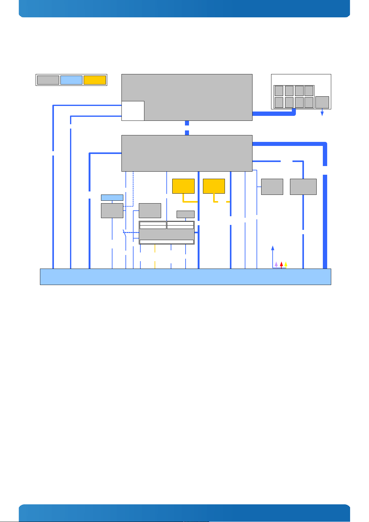
3.3 Block Diagram
15
SATA1
PwrCtrl
SysMgmt
RTC
SATA0
SATA1
SER0
SER1
DMI
PCIe#3
USB #0-7
(USB 2.0)
LPC
GPIO
SMB
PWM
FAN2
I2C
SMB
SPI
HDA
PCIe #0-2
PCIe #3
Intel® NM10
Express Chipset
LID
Sleep
TPM
SLB9635TT
SPI
BIOS Flash
LVDS
DP++
Connector Option
Standard
component
GB LAN
GPIO
Embedded Controller
(CPLD EPM570/ 1270)
HWM
NCT7802
EEPRO M
FAN1
COM Express® connector AB – Pin-out Type 10
GBLan
Intel® 82574L
VCC
5VSB
VBAT
HWM
SMB
Power sequencing
Watchdog
LPC2I2C
GPIO Buffer
SPD
DDR3-800/1066 memory down
Intel® Atom™
D2000 Series
N2000 Series
GMA3650
GMA3600
2x UART
SATA
NANDrive®
S5eco
Page 16
COMe-mCT10 / Product Specification
3.4 Accessories
Product specific accessories
Product Number Heatspreader and Cooling Solutions Comment
34005-0000-99-0 HSP COMe-mCT10 thread (11mm) For all CPUs and temperature grades
34005-0000-99-1 HSP COMe-mCT10 through (11mm) For all CPUs and temperature grades
34005-0000-99-2 HSP COMe-mCT10 slim thread (6.5mm) For all CPUs and temperature grades
34005-0000-99-3 HSP COMe-mCT10 slim though (6.5mm) For all CPUs and temperature grades
General accessories
Part Number COMe pin-out Type 10 compatible accessor ies Project Code Comment
34104-0000-00-0 COM Express® Reference Carrier-i Type 10 ADAP nITX Carrier with 8mm COMe connector
34101-0000-00-1 COM Express® Eval Carrier Type 10 ADAN ATX Eval Carrier with 8mm COMe connector
To be used in combination with ADA-Type10-Mezzanine only
34101-0000-00-2 COM Express® Eval Carrier Type 10 Gen2 ADAN ATX Eval Carrier with 8mm COMe connector
96007-0000-00-8 ADA-Type10-Mezzanine AMVV COMe basic sized stand-alone carrier or Adapter Card for Eval Carr ier
Gen1
96006-0000-00-1 COMe POST T10 NFCB POST Code / Debug Card
38019-0000-00-1 ADA-COMe-Height-single EERC Height Adapter
34104-0000-00-S COMe Ref. Starterkit T10 ADAP Starterkit with COMe Reference Carrier T10
Part Number Mounting Comment
34017-0000-00-0 COMe mMount Kit 5/8mm 1set Mounting Kit for 1 module including screws for 5mm & 8mm connectors
Part Number Cooling Solutions Comment
34099-0000-99-0 COMe mini Active Uni Cooler for CPUs up to 10W TDP, to be mounted on HSP
34099-0000-99-1 COMe mini Passive Uni Cooler for CPUs up to 5W TDP, to be mounted on HSP
34099-0000-99-2 COMe mini Passive Uni Cooler Slim for CPUs with 3-5W TDP, to be mounted on HSP
16
Page 17

COMe-mCT10 / Product Specification
3.5 Electrical Specification
3.5.1 Supply Voltage
Following supply voltage is specified at the COM Express® connector:
VCC:
4.75 - 14(20)V
Standby:
5V DC +/- 5%
RTC:
2.5V - 3.47V
- 5V Standby voltage is not mandatory for operation.
- Extended Temperature (E1) variants are validated for 12V supply only
3.5.2 Power Supply Rise Time
» The input voltages shall rise from ≤10% of nominal to within the regulation ranges within 0.1ms to 20ms.
» There must be a smooth and continuous ramp of each DC input voltage from 10% to 90% of its final set-point
following the ATX specification
3.5.3 Supply Voltage Ripple
» Maximum 100 mV peak to peak 0 – 20 MHz
3.5.4 Power Consumption
The maximum Power Consumption of the different COMe-mCT10 variants is 6.2 - 11.6W (100% CPU load on all cores; 90°C
CPU temperature). Further information with detailed measurements are available in Application Note KEMAP054 available
on EMD Customer Section. Information there is available after registration.
17
Page 18
COMe-mCT10 / Product Specification
3.5.5 ATX Mode
By connecting an ATX power supply with VCC and 5VSB, PWR_OK is set to low level and VCC is off. Press the Power Button to
enable the ATX PSU setting PWR_OK to high level and powering on VCC. The ATX PSU is controlled by the PS_ON# signal
which is generated by SUS_S3# via inversion. VCC can be 4.75 - 14(20)V in ATX Mode. On Computer-on-Modules
supporting a wide range input down to 4.75V the input voltage shall always be higher than 5V Standby (VCC > 5VSB).
State PWRBTN# PWR_OK V5_StdBy PS_ON# VCC
G3 x x 0V x 0V
S5 high low 5V high 0V
S5 S0 → PWRBTN Event low high → 5V high low → 0 V VCC →
S0 high high 5V low VCC
3.5.6 Single Supply Mode
In single supply mode (or automatic power on after power loss) without 5V Standby the module will start automatically
when VCC power is connected and Power Good input is open or at high level (internal PU to 3.3V). PS_ON# is not used in
this mode and VCC can be 4.75 - 14(20)V.
To power on the module from S5 state press the power button or reconnect VCC. Suspend/Standby States are not
supported in Single Supply Mode.
State PWRBTN# PWR_OK V5_StdBy VCC
G3 x x x 0
G3 S0 → high open / high x connecting VCC
S5 high open / high x VCC
S5 S0 → PWRBTN Event open / high x reconnecting VCC
Signals marked with “x” are not important for the specific power state. There is no
difference if connected or open.
All ground pins have to be tied to the ground plane of the carrier board.
18
Page 19
COMe-mCT10 / Product Specification
3.6 Power Control
Power Supply
The COMe-mCT10 supports a power input from 4.75 - 14(20)V. The supply voltage is applied through the VCC pins (VCC) of
the module connector.
Power Button (PWRBTN#)
The power button (Pin B12) is available through the module connector described in the pinout list. To start the module via
Power Button the PWRBTN# signal must be at least 50ms (50ms ≤ t < 4s, typical 400ms) at low level (Power Button Event).
Pressing the power button for at least 4seconds will turn off power to the module (Power Button Override).
Power Good (PWR_OK)
The COMe-mCT10 provides an external input for a power-good signal (Pin B24). The implementation of this subsystem
complies with the COM Express® Specification. PWR_OK is internally pulled up to 3.3V and must be high level to power on
the module.
Reset Button (SYS_RESET#)
The reset button (Pin B49) is available through the module connector described in the pinout list. The module will stay in
reset as long as SYS_RESET# is grounded. If available, the BIOS setting for “Reset Behavior” must be set to “Power Cycle”.
Modules with Intel® Chipset and active Management Engine do not allow to hold the
module in Reset out of S0 for a long time. At about 10s holding the reset button the ME will
reboot the module automatically
SM-Bus Alert (SMB_ALERT#)
With an external battery manager present and SMB_ALERT# (Pin B15) connected the module always powers on even if
BIOS switch “After Power Fail” is set to “Stay Off”.
19
Page 20
COMe-mCT10 / Product Specification
3.7 Environmental Specification
3.7.1 Temperature Specification
Kontron defines following temperature grades for Computer-on-Modules in general. Please see chapter 'Product
Specification' for available temperature grades for the COMe-mCT10
Temperature Specification Operating Non-operating Validated Input Voltage
Commercial grade 0°C to +60°C -30°C to +85°C VCC: 4.75 - 14(20)V
Extended Temperature (E1) -25°C to +75°C -30°C to +85°C VCC: 12V
Industrial grade by Screening (XT)
-40°C to +85°C -40°C to +85°C VCC: 12V
Industrial grade by Design (E2)
-40°C to +85°C -40°C to +85°C VCC: 4.75 - 14(20)V
Operating with Kontron heatspreader plate assembly
The operating temperature defines two requirements:
» the maximum ambient temperature with ambient being the air surrounding the module.
» the maximum measurable temperature on any spot on the heatspreader's surface
Test specification:
Temperature Grade Validation requirements
Commercial grade at 60°C HSP temperature the CPU @ 100% load needs to run at nominal frequency
Extended Temperature (E1) at 75°C HSP temperature the CPU @ 75% load is allowed to start speedstepping for thermal protection
Industrial grade by Screening (XT)
at 85°C HSP temperature the CPU @ 50% load is allowed to start throttling for thermal protection
Industrial grade by Design (E2)
at 85°C HSP temperature the CPU @ 50% load is allowed to start throttling for thermal protection
Operating without Kontron heatspreader plate assembly
The operating temperature is the maximum measurable temperature on any spot on the module's surface.
3.7.2 Humidity
» 93% relative Humidity at 40°C, non-condensing (according to IEC 60068-2-78)
20
Page 21

COMe-mCT10 / Product Specification
3.8 Standards and Certifications
RoHS II
The COMe-mCT10 is compliant to the directive 2011/65/EU on the Restriction of the use of certain Hazardous Substances
(RoHS II) in electrical and electronic equipment
Component Recognition UL 60950-1
The COM Express® mini form factor Computer-on-Modules are Recognized by Underwriters Laboratories Inc.
Representative samples of this component have been evaluated by UL and meet applicable UL requirements.
UL Listings:
» NWGQ2.E304278
» NWGQ8.E304278
WEEE Directive
WEEE Directive 2002/96/EC is not applicable for Computer-on-Modules.
Conformal Coating
Conformal Coating is available for Kontron Computer-on-Modules and for validated SO-DIMM memory modules. Please
contact your local sales or support for further details.
21
Page 22

COMe-mCT10 / Product Specification
Shock & Vibration
The COM Express® mini form factor Computer-on-Modules successfully passed shock and vibration tests according to
» IEC/EN 60068-2-6 (Non operating Vibration, sinusoidal, 10Hz-4000Hz, +/-0.15mm, 2g)
» IEC/EN 60068-2-27 (Non operating Shock Test, half-sinusoidal, 11ms, 15g)
EMC
Validated in Kontron reference housing for EMC the COMe-mCT10 follows the requirements for electromagnetic
compatibility standards
» EN55022
22
Page 23

COMe-mCT10 / Product Specification
3.9 MTBF
The following MTBF (Mean Time Before Failure) values were calculated using a combination of manufacturer’s test data, if
the data was available, and the Telcordia (Bellcore) issue 2 calculation for the remaining parts.
The calculation method used is “Telcordia Issue 2 Method 1 Case 3” in a ground benign, controlled environment (GB,GC).
This particular method takes into account varying temperature and stress data and the system is assumed to have not
been burned in.
Other environmental stresses (extreme altitude, vibration, salt water exposure, etc) lower MTBF values.
System MTBF (hours): 209259 @ 40°C (w/PCB)
Fans usually shipped with Kontron Europe GmbH products have 50,000-hour typical
operating life. The above estimates assume no fan, but a passive heat sinking arrangement
Estimated RTC battery life (as opposed to battery failures) is not accounted for in the above
figures and need to be considered separately. Battery life depends on both temperature
and operating conditions. When the Kontron unit has external power; the only battery
drain is from leakage paths.
23
Page 24
COMe-mCT10 / Product Specification
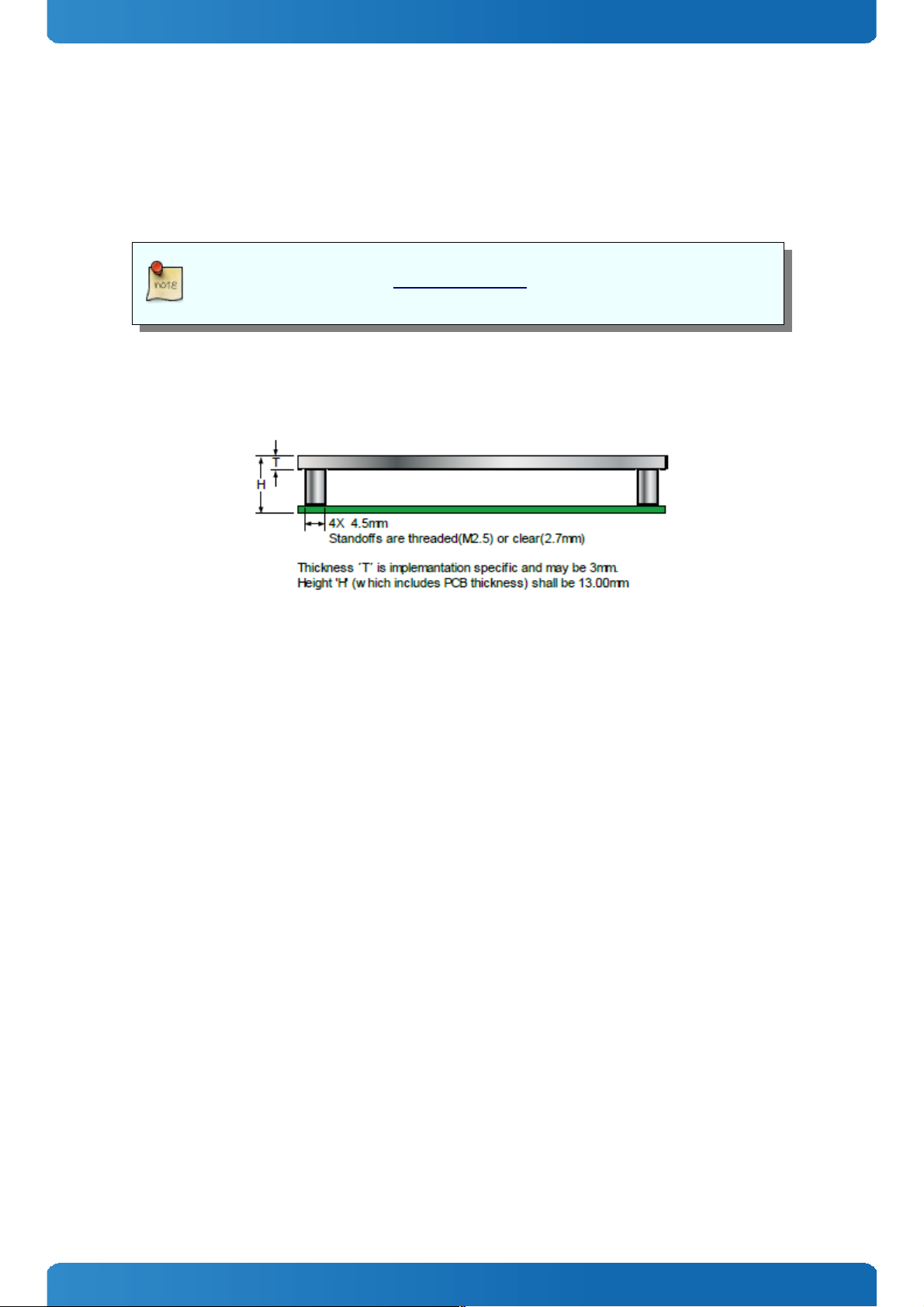
3.10 Mechanical Specification
Module Dimension
» 55mm x 84mm (±0.2mm)
» Height approx. 3.5mm (withouth printed circuit board)
CAD drawings are available at EMD CustomerSection
Height
The COM Express® specification defines a module height of 13mm from bottom to heatspreader top:
Kontron provides standard HSP for the specified height of 13mm and slim-line Heatspreader for a reduced height of
8.5mm for mini sized Computer-on-Modules. Universal Cooling solutions to be mounted on the HSP are 14.3mm (340990000-00-0/1) or 8mm (34099-0000-00-2) in height. This allows combinations of a total module height of 8.5mm or
13mm with the Heatspreader and between 16.5mm and 27.3mm with a cooling solution.
24
Page 25

COMe-mCT10 / Product Specification
3.11 Thermal Management, Heatspreader and Cooling Solutions
A heatspreader plate assembly is available from Kontron Europe GmbH for the COMe-mCT10. The heatspreader plate on top
of this assembly is NOT a heat sink. It works as a COM Express®-standard thermal interface to use with a heat sink or
external cooling devices.
External cooling must be provided to maintain the heatspreader plate at proper operating temperatures. Under worstcase conditions, the cooling mechanism must maintain an ambient air and heatspreader plate temperature on any spot of
the heatspreader's surface according the module specifications:
» 60°C for commercial grade modules
» 75°C for extended temperature grade modules (E1)
» 85°C for industrial temperature grade modules (E2/XT)
The aluminum slugs and thermal pads or the heat-pipe on the underside of the heatspreader assembly implement thermal
interfaces between the heatspreader plate and the major heat-generating components on the COMe-mCT10. About 80
percent of the power dissipated within the module is conducted to the heatspreader plate and can be removed by the
cooling solution.
You can use many thermal-management solutions with the heatspreader plates, including active and passive approaches.
The optimum cooling solution varies, depending on the COM Express® application and environmental conditions. Active
or passive cooling solutions provided from Kontron Europe GmbH for the COMe-mCT10 are usually designed to cover the
power and thermal dissipation for a commercial grade temperature range used in a housing with proper air flow.
Documentation and CAD drawings of COMe-mCT10 heatspreader and cooling solutions are provided at
http://emdcustomersection.kontron.com.
25
Page 26
COMe-mCT10 / Product Specification
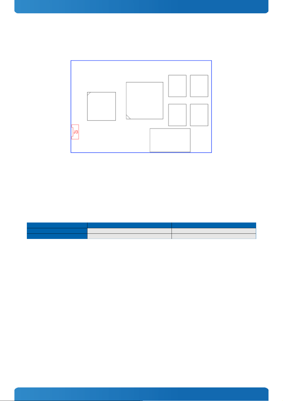
3.12 Onboard Fan Connector
Variants with D2550 and N2800 are equipped with an onboard FAN connector for active cooling controlled by the BIOS.
Location of the FAN Connector on top
Specification of the FAN Connector:
» Part number (Molex) J3: 53261-0371
» Mates with: 51021-0300
» Crimp terminals: 50079-8100
Pin assignment
» Pin1: Tacho, Pin2: VCC, Pin3: GND
Electrical characteristic
Module Input Voltage 4.75 - 13V >13
FAN Output Voltage
4.75 - 13V 13V
Max. FAN Output Current
350mA 150mA
26
Page 27
COMe-mCT10 / Features and Interfaces
4 Features and Interfaces
4.1 Onboard SSD
The COMe-mCT10 features an onboard Greenliant SATA NAND flash drive with capacities of 2-32GB SLC, 2-64GB MLC
(SATA). Due to performance and longevity reasons standard variants with onboard flash use SLC type only. The following
SATA NANDrives are available:
Basic features of the SATA NANDrives
» ATA/ATAPI-8 compliant Host interface with 48-bit address feature set and SMART support
» RoHS compliant NAND flash type
» SATA 1.5Gb/s Host transfer rate
» Hardware error detection, correction ECC and advanced wear leveling
» Bad block management
» TRIM support
» SMART support
» 0°C to +70°C temperature range for MLC types A-M-C/B-M-C
» -40°C to +85°C temperature range for MLC types B-M-I
» -40°C to +85°C temperature range for all SLC types
Single-level Cell (SLC) NANDrive™
Flash Part No. GLS85LS
Flash Part No. 1002P-S-I-FZJE-ND104 1004P-S-I-FZJE-ND104 1008P-S-I-FZJE-ND104 1016P-S-I-FZJE-ND104 1032P-S-I-FZJE-ND104
Product Revision
CC1 CC1 CC1 CC1 CC1
Flash Size 2GByte 4GByte 8GByte 16GByte 32GByte
Burst Read/Write Speed
35/20 MB/s 70/35 MB/s 70/50 MB/s 70/55 MB/s 120/80 MB/s
Total Bytes
2,000,388,096 4,001,292,288 8,012,390,400 16,013,942,784 32,017,047,552
Active Mode Power
450mW 560mW 750mW 590mW 855mW
Typical P/E Cycles per
block
100,000 100,000 60,000 60,000 60,000
(Data based on Datasheet S71432 Rev. 03.100 from 11-2013 and S71445 Rev. 01.400 from 11-2013)
Multi-level Cell (MLC) NANDrive™
Flash Part No. GLS85LS
Flash Part No.
1002A-M-C-FZJE-ND103
1002A-M-I-FZJE-ND103
1004A-M-C-FZJE-ND103
1004A-M-I-FZJE-ND103
1008B-M-C-FZJE-ND103
1008B-M-I-FZJE-ND103
1016B-M-C-FZJE-ND103
1016B-M-I-FZJE-ND103
1032B-M-C-FZJE-ND103
1032B-M-I-FZJE-ND103
1064B-M-C-FZJE-ND103
1064B-M-I-FZJE-ND103
Product Revision
CB2 CB2 CB2 CB2 CB2 CB2
Flash Size 2GByte 4GByte 8GByte 16GByte 32GByte 64GByte
Burst Read/Write
Speed
35/10 MB/s 35/10 MB/s 35/10 MB/s 70/20 MB/s 70/30 MB/s 110/60 MB/s
Total Bytes
1,941,553,152 3,941,941,248 8,012,390,400 16,013,942,784 32,017,047,552 64,023,257,088
Active Mode Power
360mW 360mW 360mW 440mW 565mW 820mW
Typical P/E Cycles per
block
5,000 5,000 5,000 5,000 5,000 5,000
(Data based on Datasheet S71430 Rev 02.00 from 10-2013)
27
Page 28

COMe-mCT10 / Features and Interfaces
4.2 S5 Eco Mode
Kontron’s new high-efficient power-off state S5 Eco enables lowest power-consumption in soft-off state – less than 1 mA
compared to the regular S5 state this means a reduction by at least factor 200!
In the “normal” S5 mode the board is supplied by 5V_Stb and needs usually up to 300mA just to stay off. This mode allows
to be switched on by power button, RTC event and WakeOnLan, even when it is not necessary. The new S5 Eco mode
reduces the current enormous.
The S5 Eco Mode can be enabled in BIOS Setup, when the BIOS supports this feature.
Following prerequisites and consequences occur when S5 Eco Mode is enabled
» The power button must be pressed at least for 200ms to switch on.
» Wake via Power button only.
» “Power On After Power Fail”/“State after G3”: only “stay off” is possible
28
Page 29
COMe-mCT10 / Features and Interfaces
4.3 LPC
The Low Pin Count (LPC) Interface signals are connected to the LPC Bus bridge located in the CPU or chipset. The LPC low
speed interface can be used for peripheral circuits such as an external Super I/O Controller, which typically combines
legacy-device support into a single IC. The implementation of this subsystem complies with the COM Express®
Specification. Implementation information is provided in the COM Express® Design Guide maintained by PICMG. Please
refer to the official PICMG documentation for additional information.
The LPC bus does not support DMA (Direct Memory Access) and a clock buffer is required when more than one device is
used on LPC. This leads to limitations for ISA bus and SIO (standard I/O´s like Floppy or LPT interfaces) implementations.
All Kontron COM Express® Computer-on-Modules imply BIOS support for following external baseboard LPC Super I/O
controller features for the Winbond/Nuvoton 5V 83627HF/G and 3.3V 83627DHG-P:
83627HF/G Phoenix BIOS AMI CORE8 AMI / Phoenix EFI
PS/2 YES YES YES
COM1/COM2 YES YES YES
LPT YES YES YES
HWM YES YES NO
Floppy NO NO NO
GPIO NO NO NO
83627DHG-P Phoenix BIOS AMI CORE8 AMI / Phoenix EFI
PS/2 YES YES YES
COM1/COM2 YES YES YES
LPT YES YES YES
HWM NO NO NO
Floppy NO NO NO
GPIO NO NO NO
Features marked as not supported do not exclude OS support (e.g. HWM can be accessed via SMB). For any other LPC
Super I/O additional BIOS implementations are necessary. Please contact your local sales or support for further details.
29
Page 30
COMe-mCT10 / Features and Interfaces
4.4 Serial Peripheral Interface (SPI)
The Serial Peripheral Interface Bus or SPI bus is a synchronous serial data link standard named by Motorola that operates
in full duplex mode. Devices communicate in master/slave mode where the master device initiates the data frame.
Multiple slave devices are allowed with individual slave select (chip select) lines. Sometimes SPI is called a “four wire”
serial bus, contrasting with three, two, and one wire serial buses.
The SPI interface can only be used with a SPI flash device to boot from external BIOS on the
baseboard.
4.5 SPI boot
The COMe-mCT10 supports boot from an external SPI Flash. It can be configured by pin A34 (BIOS_DIS#0) and pin B88
(BIOS_DIS1#) in following configuration:
BIOS_DIS0# BIOS_DIS1# Function
open open Boot on-module BIOS
GND open Boot baseboard LPC FWH
open GND Baseboard SPI = Boot Device 1, on-module SPI = Boot Device 2
GND GND Baseboard SPI = Boot Device 2, on-module SPI = Boot Device 1
By default only SPI Boot Device 1 is used in configuration 3 & 4. Both SPI Boot Devices are
used by splitting the BIOS with modified descriptor table in customized versions only
Recommended SPI boot flash types for 8-SOIC package
Size Manufacturer Part Number Device ID
16Mbit Atmel AT26DF161 0x1F4600
16Mbit Atmel AT26DF161A 0x1F4601
16Mbit Atmel AT25DF161 0x1F4602
16Mbit Atmel AT25DQ161 0x1F8600
16Mbit Macronix MX25L1605A(D)(36E)(06E) 0xC22015
16Mbit Macronix MX25L1635D 0xC22415
16Mbit SST/Microchip SST25VF016B 0xBF2541
16Mbit Winbond W25X16BV 0xEF3015
16Mbit Winbond W25Q16BV(CV) 0xEF4015
Size Manufacturer Part Number Device ID
32Mbit Atmel AT25/26DF321 0x1F4700
32Mbit Atmel AT25DF321A 0x1F4701
32Mbit Macronix MX25L3205A(D)(06E) 0xC22016
32Mbit Macronix MX25L3225D(35D)(36D) 0xC25E16
32Mbit SST/Microchip SST25VF032B 0XBF254A
32Mbit Winbond W25X32BV 0xEF3016
32Mbit Winbond W25Q32BV, 0xEF4016
Size Manufacturer Part Number Device ID
64Mbit Atmel AT25DF641(A) 0x1F4800
64Mbit Atmel AT25DQ641 0x1F8800
64Mbit Macronix MX25L6405D(45E)(36E)(06E)(73E) 0xC22017
64Mbit Macronix MX25L6455E 0xC22617
64Mbit Macronix MX25U6435F 0xC22537
64Mbit SST/Microchip SST25VF064C 0xBF254B
64Mbit Winbond W25X64BV 0xEF3017
64Mbit Winbond W25Q64BV(CV)(FV) 0xEF4017
64Mbit Winbond W25Q64DW 0XEF6017
64Mbit Winbond W25Q64FW 0XEF6017
30
Page 31

COMe-mCT10 / Features and Interfaces
Using an external SPI flash
To program an external SPI flash follow these steps:
» Connect a SPI flash with correct size (similar to BIOS ROM file size) to the module SPI interface
» Open pin A34 and B88 to boot from the module BIOS
» Boot the module to DOS/EFI-Shell with access to the BIOS image and Firmware Update Utility provided on EMD
Customer Section
» Connect pin B88 (BIOS_DIS1#) to ground to enable the external SPI flash
» Execute Flash.bat/Flash.efi to program the complete BIOS image to the external SPI flash
» reboot
Your module will now boot from the external SPI flash when BIOS_DIS1# is grounded.
External SPI flash on Modules with Intel® ME
If booting from the external (baseboard mounted) SPI flash then exchanging the COM Express® module for another one
of the same type will cause the Intel® Management Engine to fail during next start. This is by design of the ME because it
bounds itself to the very module it has been flashed to. In the case of an external SPI flash this is the module present at
flash time.
To avoid this issue please make sure to conduct a complete flash of the external SPI flash device after changing the
COMexpress module for another one. If disconnecting and reconnecting the same module again this step is not necessary.
31
Page 32

COMe-mCT10 / Features and Interfaces
4.6 M.A.R.S.
The Smart Battery implementation for Kontron Computer-on-Modules called Mobile Application for Rechargeable Systems
is a BIOS extension for external Smart Battery Manager or Charger. It includes support for SMBus charger/selector (e.g.
Linear Technology LTC1760 Dual Smart Battery System Manager) and provides ACPI compatibility to report battery
information to the Operating System.
Reserved SM-Bus addresses for Smart Battery Solutions on the carrier:
8-bit Address 7-bit Address Device
12h 0x09 SMART_CHARGER
14h 0x0A SMART_SELECTOR
16h 0x0B SMART_BATTERY
32
Page 33

COMe-mCT10 / Features and Interfaces
4.7 UART
The COMe-mCT10 supports up to two Serial RX/TX only Ports defined in COM Express® specification on Pins A98/A99 for
UART0 and Pins A101/A102 for UART1. The implementation of the UART is compatible to 16450 and is supported by
default from most operating systems. Resources are subordinated to other UARTS e.g. from external LPC Super I/O.
UART features:
» 450 to 115.2k Baud (except 56000)
» 5, 6, 7 or 8bit characters
» 1 or 2 Stop bit generation
» Even, odd or no-parity generation/detection
» Complete status reporting capabilities
» Line break generation and detection
» Full prioritized interrupt system control
» No FIFO
» One additional shift register for transmit and one for receive
» No Flow Control
» No FCR register due to unavailability of FIFO
» MCR and MSR registers only implemented in loopback mode for compatibility with existing drivers and APIs
» Initialized per default to COM3 3F8h/IRQ4 and COM4 2F8/IRQ3 without external SIO
» Initialized per default to COM3 3E8h/IRQ5 and COM4 2E8/IRQ10 with external SIO present
The UART clock is generated by the 33MHz LPC clock which results in an accuracy of 0.5% on all UART timings
- Due to the protection circuitry required according COM Express® specification the
transfer speed can only be guaranteed for 9600 Baud. Please contact your local sales or
support for customized versions without protection circuitry
- Legacy console redirection via onboard serial ports may be restricted in terms of serial
input stream. Since they're only emulating a 16450 device (w/o FIFO) an input stream
generated by a program may lose characters. Inputs from a keyboard via terminal program
will be safe.
33
Page 34

COMe-mCT10 / Features and Interfaces
4.8 Fast I2C
The COMe-mCT10 supports a CPLD implemented LPC to I2C bridge using the WISHBONE I2C Master Core provided from
opencores.org. The I2C Interface supports transfer rates up to 40kB/s and can be configured in Setup
Specification for external I2C:
» Speed up to 400kHz
» Compatible to Philips I2C bus standard
» Multi-Master capable
» Clock stretching support and wait state generation
» Interrupt or bit-polling driven byte-by-byte data-transfers
» Arbitration lost interrupt with automatic transfer cancellation
» Start/Stop signal generation/detection
» Bus busy detection
» 7bit and 10bit addressing
34
Page 35

COMe-mCT10 / Features and Interfaces
4.9 GPIO - General Purpose Input and Output
The COMe-mCT10 offers 4 General Purpose Input (GPI) pins and 4 General Purpose Output (GPO) pins. On a 3.3V level
digital in- and outputs are available.
Signal Pin Description
GPI0 A54 General Purpose Input 0
GPI1 A63 General Purpose Input 1
GPI2 A67 General Purpose Input 2
GPI3 A85 General Purpose Input 3
GPO0 A93 General Purpose Output 0
GPO1 B54 General Purpose Output 1
GPO2 B57 General Purpose Output 2
GPO3 B63 General Purpose Output 3
Configuration
The GPI and GPO pins can be configured via JIDA32/K-Station. Please refer to the JIDA32/K-Station manual in the driver
download packet on our customer section.
35
Page 36

COMe-mCT10 / Features and Interfaces
4.10 Dual Staged Watchdog Timer
Basics
A watchdog timer (or computer operating properly (COP) timer) is a computer hardware or software timer that triggers a
system reset or other corrective action if the main program, due to some fault condition, such as a hang, neglects to
regularly service the watchdog (writing a “service pulse” to it, also referred to as “kicking the dog”, “petting the dog”,
“feeding the watchdog” or “triggering the watchdog”). The intention is to bring the system back from the nonresponsive
state into normal operation.
The COMe-mCT10 offers a watchdog which works with two stages that can be programmed independently and used one by
one.
Time-out events
Reset
A reset will restart the module and starts POST and operating system new.
NMI
A non-maskable interrupt (NMI) is a computer processor interrupt that cannot be ignored by st andard interrupt masking techniques in the system. It
is typically used to signal attention for non-recoverable hardware errors.
SCI
A system control interrupt (SCI) is a OS-visible interrupt to be handled by the OS using AML code
Delay
Might be necessary when an operating system must be started and the time for the first trigger pulse must extended. (Only available in the f irst
stage)
WDT Signal only
This setting triggers the WDT Pin on baseboard connector (COM Express® Pin B27) only
Cascade:
Does nothing, but enables the 2nd stage af ter the entered time-out.
WDT Signal
B27 on COM Express® Connector offers a signal that can be asserted when a watchdog timer has not been triggered within
time. It can be configured to any of the 2 stages. Deassertion of the signal is automatically done after reset. If
deassertion during runtime is necessary please ask your Kontron technical support for further help.
36
Page 37

COMe-mCT10 / Features and Interfaces
4.11 Intel® Fast Flash Standby™ / Rapid Start Technology™
The target of Intel® Fast Flash Standby™ (iFFS) (also known as Intel® Rapid Start Technology™ iRST) is to get a wake-up
time from S4 compareable to S3. Normally S4 is caused by OS which stores it's information to the hard disk and does then
a normal shutdown. S4 resume takes quite long as the system does a normal BIOS POST and OS restores it's information
from the hard disk.
IFFS does it in a different way. The Operating System initiates an S3 and stores it's information in memory. After that
BIOS copies this OS information from DRAM to SSD and does a sleep state similar to S4 with nearly zero power. If system is
resumed by power button, BIOS restores memory content from SSD to the DRAM and does an S3 resume which is much
faster.
Requirements
» SATA Solid State Disk in AHCI mode
» Free disk space on the SSD with at least the DRAM size
» Operating System with disk partition tool to allocate the hibernation partition (e.g. Windows 7/8)
» BIOS supporting iFFS feature
How to setup once the operating system is installed
» Prepare a free disk space on your onboard or external SSD with at least the size of DRAM
» Open cmd.exe in Administrator Mode and type diskpart.exe to open the Windows disk partition tool
» DISKPART> list disk
» DISKPART> select disk X (X is disk number where you want to create the store partition. Refer to results from “list
disk” for exact disk number)
» DISKPART> create partition primary
» DISKPART> detail disk
» DISKPART> select Volume X (X is Volume of your store partition. Refer to results from “detail disk” for exact volume
number)
» DISKPART> set id=84 override (ID 84 marks the partition as hibernate partition)
» DISKPART> exit
» Now there should be a Hibernate Partition visible in your disk management
» Reboot and enable iFFS in BIOS
Usage
» Activate Lid / move system to Sleep/Standby ( S3)→
» After configured period of time in Setup the system powers on automatically and information in DRAM moves to
non-volatile memory (Default is 'immediately')
» System switches off again to iFFS ( comparable to S4, Power Supply can now be disconnected)→
» When System is powered on, information moved back to DRAM (No display output during copy process)
» System resumes same as Sleep/Standby S3
Note
» Depending on the platform iFFS enabled may disable the hibernate function in Windows automatically
37
Page 38

COMe-mCT10 / Features and Interfaces
Benefits
» System transitions from S3 to S4 automatically
» Up to 6x battery life compared to Standby
» Resume time reduced up to 75%
Measured resume times from Power-on to Win7 Log-on Screen on COMe-mCT10:
» 2.5” SATA II HDD 5400rpm: Hibernate: 22s, iFFs on onboard NANDrive: 17s
» 2.5” SATA III SSD: Hibernate: 18s, iFFS on SSD: 10s
38
Page 39

COMe-mCT10 / Features and Interfaces
4.12 Speedstep Technology
The Intel® processors offer the Intel® Enhanced SpeedStep™ technology that automatically switches between maximum
performance mode and battery-optimized mode, depending on the needs of the application being run. It enables you to
adapt high performance computing on your applications. When powered by a battery or running in idle mode, the
processor drops to lower frequencies (by changing the CPU ratios) and voltage, conserving battery life while maintaining
a high level of performance. The frequency is set back automatically to the high frequency, allowing you to customize
performance.
In order to use the Intel® Enhanced SpeedStep™ technology the operating system must support SpeedStep™ technology.
By deactivating the SpeedStep feature in the BIOS, manual control/modification of CPU performance is possible. Setup
the CPU Performance State in the BIOS Setup or use 3rd party software to control CPU Performance States.
39
Page 40

COMe-mCT10 / Features and Interfaces
4.13 C-States
New generation platforms include power saving features like SuperLFM, EIST (P-States) or C-States in O/S idle mode.
Activated C-States are able to dramatically decrease power consumption in idle mode by reducing the Core Voltage or
switching of parts of the CPU Core, the Core Clocks or the CPU Cache.
Following C-States are defined:
C-State Description Function
C0 Operating CPU fully turned on
C1 Halt State Stops CPU main internal clocks via sof tware
C1E Enhanced Halt Similar to C1, additionally reduces CPU voltage
C2 Stop Grant Stops CPU internal and external clocks via hardware
C2E Extended Stop Grant Similar to C2, additionally reduces CPU voltage
C3 Deep Sleep Stops all CPU internal and external clocks
C3E Extended Stop Grant Similar to C3, additionally reduces CPU voltage
C4 Deeper Sleep Reduces CPU voltage
C4E Enhanced Deeper Sleep Reduces CPU voltage even more and turns off the memory cache
C6 Deep Power Down Reduces the CPU internal voltage to any value, including 0V
C7 Deep Power Down Similar to C6, additionally LLC (LastLevelCache) is switched of f
C-States are usually enabled by default for low power consumption, but active C-States my influence performance
sensitive applications or real-time systems.
» Active C6-State may influence data transfer on external Serial Ports
» Active C7-State may cause lower CPU and Graphics performance
It's recommended to disable C-States / Enhanced C-States in BIOS Setup if any problems occur.
40
Page 41

COMe-mCT10 / Features and Interfaces
4.14 Hyper Threading
Hyper Threading (officially termed Hyper Threading Technology or HTT) is an Intel®-proprietary technology used to
improve parallelization of computations performed on PC´s. Hyper-Threading works by duplicating certain sections of the
processor—those that store the architectural state but not duplicating the main execution resources. This allows a HyperThreading equipped processor to pretend to be two “logical” processors to the host operating system, allowing the
operating system to schedule two threads or processes simultaneously. Hyper Threading Technology support always relies
on the Operating System.
41
Page 42

COMe-mCT10 / Features and Interfaces
4.15 Graphics Features
The COMe-mCT10 supports the integrated Intel® GMA 3650 / 3600 graphics based on PowerVR SGX545. Following
Operating System and Software Features are supported:
O/S WEC7 WinXP / XPe Win7 / WES7 Linux Fedora / Yocto
Recommended VBIOS
EMGD* GMA*
Driver
EMGD 1.15 EMGD 1.15 GMA 3600 Linux PowerVR Graphics
Max LVDS Resolution
D2000: 1440×900
N2000: 1366×768
Max VGA Resolution
D2000/N2000: 1920×1200
Max HDMI/DVI Resolution
D2000/N2000: 1920×1200
Max DP Resolution
D2000: 2560×1600
N2000: 1920×1200
D2000: 2560×1600
N2000: 1600×1200
Max eDP Resolution
D2000: 1920×1080 (1080p)
N2000: 1366×768
Dual Independent Display
Yes
2D HW Acceleration
- DirectDraw DirectDraw EXA and XRandR
3D HW Acceleration
- DX9 Direct3D DX9 Direct3D OpenGL ES2.0, HTML5WebGL
HW Media Acceleration
SW only SW only DXVA VA API
HW Codecs supported
- - H.264, MPEG2, VC-1 H.264, MPEG2
Blu-Ray
- - v2.0 -
HDCP
- v1.3 (HDMI only) v1.3 (HDMI/DP) -
Media players
- - Windows Media Player
PowerDVD 10
Total Media Theatre 3
MPlayer
* The Standard BIOS provided with the module supports the GMA VBIOS only. For any issues
of EMGD driver in combination with GMA VBIOS please contact your local sales or support
4.16 Hardware Configuration
The Intel® GMA 3650 / 3600 supports 2 Digital Display Interfaces:
» DDI0 = HDMI-B or DP-B
» DDI1 = HDMI-C or DP-C
On COMe-mCT10 only DDI1 is available while on COMe-cCT6 both DDIs are provided on COM Express connector
4.17 Graphics VBIOS and Driver
The COMe-mCT10 standard BIOS supports the GMA Video-BIOS which is optimized for use with GMA Video Driver
(Win7/WES7). For use with EMGD driver (Linux, WinXP) Intel® recommends to use the EMGD Video-BIOS. The EMGD VBIOS
has to be configured for each System Layout and Display Configuration separately which only allows to use the EMGD
VBIOS within a customized BIOS Version. To prepare a EMG Driver and EMGD VBIOS following software is required:
» Intel® EMGD package: available on EMD Customer Section
» Documentation how to prepare a driver and VBIOS: Inside EMGD Package
» C++ Compiler to create a VBIOS
» AMI MMTool to patch the VBIOS into the Module BIOS
Please contact your local Sales or support for further details or preparing a customized BIOS according your requirements
42
Page 43

COMe-mCT10 / Features and Interfaces
4.18 ACPI Suspend Modes and Resume Events
The COMe-mCT10 supports the S-states S0, S3, S4, S5. S5eco Support: YES
The following events resume the system from S3:
» USB Keyboard (1)
» USB Mouse (1)
» Power Button
» WakeOnLan (2)
The following events resume the system from S4:
» Power Button
» WakeOnLan (2)
The following events resume the system from S5:
» Power Button
» WakeOnLan (2)
The following events resume the system from S5Eco:
» Power Button
(1) OS must support wake up via USB devices and baseboard must power the USB Port with
StBy-Voltage
(2) Depending on the Used Ethernet MAC/Phy WakeOnLan must be enabled in BIOS setup
and driver options
43
Page 44

COMe-mCT10 / Features and Interfaces
4.19 USB
The COMe-mCT10 supports 8x USB 2.0 with following internal EHCI/UHCI configuration inside .
44
Page 45

COMe-mCT10 / System Resources
5 System Resources
5.1 Interrupt Request (IRQ) Lines
IRQ # Used For Available Comment
0 Timer0 No -
1 Keyboard No -
2 Cascade No -
3 External SIO - COM2 Ext.SIO Dynamic (BIOS default)
4 External SIO - COM1 Ext.SIO Dynamic (BIOS default)
5 External SIO - LPT1 Ext.SIO Dynamic (BIOS default)
6 - Ext.SIO -
7 SMBus No Note(3)
8 RTC No -
9 ACPI No -
10 - Ext.SIO -
11 - Ext.SIO -
12 - Ext.SIO -
13 FPU No -
14 - No -
15 - No -
16 LNK A No PCIe RP 0 + USB UHCI3; Note(3)
17 LNK B No PCIe RP 1; Note(3)
18 LNK C No PCIe RP 2 + USB UHCI2 + SDIO; Note(3)
19 LNK D No PCIe RP 3 + USB UHCI1 + S-ATA; Note(3)
20 LNK E No Note(3)
21 LNK F No Note(3)
22 LNK G No HDA; Note(3)
23 LNK H No USB UHCI0 + USB EHCI; Note(3)
(1) If the “Used For” device is disabled in setup, the corresponding interrupt is available
for other device.
(2) Not available if ACPI is used
(3) ACPI OS decides on particular IRQ usage
5.2 Memory Area
The first 640 kB of DRAM are used as main memory. Using DOS, you can address 1MB of memory directly. The memory area
above 1 MB (high memory, extended memory) is accessed under DOS via special drivers such as HIMEM.SYS and
EMM386.EXE, which are part of the operating system. Please refer to the operating system documentation or special
textbooks for information about HIMEM.SYS and EMM386.EXE. Other operating systems (Linux or Windows versions) allow
you to address the full memory area directly.
Upper Memory Used for Available Comment
A0000h – BFFFFh VGA Memory No Mainly used by graphic controller
C0000h – CFFFFh VGA BIOS No Used by onboard VGA ROM
D0000h – DFFFFh - Yes Free for shadow RAM in st andard
configurations.
E0000h – FFFFFh System BIOS No Fixed
E0000000h–EFFFFFFFh PCIe Config Space No Fixed
FEC00000h-FEC00FFFh APCB No Fixed
FED00000h-FED003FFh HPET No Fixed
FED14000h-FED17FFFh MCH No Fixed
FED18000h-FED18FFFh DMI No Fixed
FED19000h-FED19FFFh EPBA No Fixed
FED1C000h-FED1FFFFh RCBA No Fixed
FED2000h FED8FFFFh Chipset + TPM No Fixed
FF000000h-FFFFFFFFh BIOS Flash No Fixed
45
Page 46

COMe-mCT10 / System Resources
5.3 I/O Address Map
The I/O-port addresses of the are functionally identical to a standard PC/AT. All addresses not mentioned in this table
should be available. We recommend that you do not use I/O addresses below 0100h with additional hardware for
compatibility reasons, even if available.
I/O Address Used for Available Comment
0000 - 001F System Ressources No Fixed
0020 - 003F Interrupt Controller 1 No Fixed
0040 - 005F Timer, Counter No Fixed
0060 - 006F Keyboard controller No Fixed
0070 - 007F RTC and CMOS Registers No Fixed
0080 BIOS Postcode No Fixed
0081 - 009F DMA Controller No Fixed
00A0 - 00BF Interrupt Controller No Fixed
00C0 - 00DF DMA Controller No F ixed
00F0 - 00FF Math Coprocessor No Fixed
0290 - 029F Ext.SIO No Fixed
03B0 - 03DF VGA No Fixed
0400 - 047F Chipset No Fixed
04D0 - 04D1 Chipset No Fixed
0500 - 057F Chipset No Fixed
0600 - 061F Chipset No Fixed
0680 - 06FF Chipset No Fixed
0A80 - 0A81 CPLD No Fixed
0CF8 - 0CFF Chipset No Fixed
5.4 Peripheral Component Interconnect (PCI) Devices
All devices follow the Peripheral Component Interconnect 2.3 (PCI 2.3) respectivily the PCI Express Base 1.0a
specification. The BIOS and OS control memory and I/O resources. Please see the PCI 2.3 specification for details.
PCI Device B:D:F PCI IRQ Inter face Comment
Host Bridge 0:00:0 - internal Chipset
Video Controller 0:02:0 LNK A internal Chipset
HDA 0:1B:0 LNK G PCIe Chipset
PCIe Port 0 0:1C:0 LNK A internal Chipset
PCIe Port 0 Slot - A/B/C/D PCIe Por t 0
PCIe Port 1 0:1C:1 LNK A internal Chipset
PCIe Port 1 Slot - B/C/D/A PCIe Por t 1
PCIe Port 2 0:1C:2 LNK A internal Chipset
PCIe Port 2 Slot - C/D/A/B PCIe Por t 2
PCIe Port 3 0:1C:3 LNK A internal Chipset
PCIe Port 3 Slot - D/A/B/C PCIe Por t 3
UHCI0 0:1D:0 LNK H internal Chipset
UHCI1 0:1D:1 LNK D internal Chipset
UHCI2 0:1D:2 LNK C internal Chipset
UHCI3 0:1D:3 LNK A internal Chipset
EHCI 0:1D:7 LNK H internal Chipset
LPC Bridge 0:1F:0 - internal Chipset
SATA 0:1F:2 LNK D internal Chipset
SMBus 0:1F:3 LNK D internal Chipset
GbE X:00:0 LNK D PCIe Slot 3
46
Page 47

COMe-mCT10 / System Resources
5.5 I2C Bus
I2C Address Used For Available Comment
A0h FRU-EEPROM No Module EEPROM
AEh FRU-EEPROM No Baseboard EEPROM
5.6 JILI I2C Bus
I2C Address Used For Available Comment
A0h LVDS-EEPROM No EEPROM for LVDS Data
5.7 System Management (SM) Bus
Address Device Comment
12h SMART_CHARGER Not to be used with any SM bus deivce except a charger
14h SMART_SELECTOR Not to be used with any SM bus deivce except a selector
16h SMART_BATTERY Not to be used with any SM bus deivce except a battery
58h HWMonitor Do not use under any circumstances
A0h DDR3 channel A Do not use under any circumstances
A2h DDR3 channel B Do not use under any circumstances
D2h Clock Generator Do not use under any circumstances
47
Page 48

COMe-mCT10 / Pinout List
6 Pinout List
6.1 General Signal Description
Type Description
I/O-3,3
Bi-directional 3,3 V IO-Signal
I/O-5T
Bi-dir. 3,3V I/O (5V Tolerance)
I/O-5
Bi-directional 5V I/O-Signal
I-3,3
3,3V Input
I/OD
Bi-directional Input/Output Open Drain
I-5T
3,3V Input (5V Tolerance)
OA
Output Analog
OD
Output Open Drain
O-1,8
1,8V Output
O-3,3
3,3V Output
O-5
5V Output
DP-I/O
Differential Pair Input/Output
DP-I
Differential Pair Input
DP-O
Differential Pair Output
PU
Pull-Up Resistor
PD
Pull-Down Resistor
PWR
Power Connection
To protect external power lines of peripheral devices, make sure that: the wires have the
right diameter to withstand the maximum available current the enclosure of the peripheral
device fulfills the fire-protection requirements of IEC/EN60950
48
Page 49

COMe-mCT10 / Pinout List
6.2 Connector X1A Row A
Pin Signal Description Type Termination Comment
A1 GND_1 Power Ground PWR - -
A2 GBE0_MDI3- Ethernet Receive Data- DP-I - -
A3 GBE0_MDI3+ Ethernet Receive Data+ DP-I - -
A4 GBE0_LINK100# Ethernet Speed LED 100Mbps OD - -
A5 GBE0_LINK1000# Ethernet Speed LED 1000Mbps OD - -
A6 GBE0_MDI2- Ethernet Receive Data- DP-I - -
A7 GBE0_MDI2+ Ethernet Receive Data+ DP-I - -
A8 GBE0_LINK# LAN Link LED OD - -
A9 GBE0_MDI1- Ethernet Receive Data- DP-I - -
A10 GBE0_MDI1+ Ethernet Receive Data+ DP-I - -
A11 GND_2 Power Ground PWR - -
A12 GBE0_MDI0- Ethernet Transmit Data- DP-O - -
A13 GBE0_MDI0+ Ethernet Transmit Data+ DP-O - -
A14 GBE0_CTREF LAN Reference Voltage O-3.3 100nF to GND -
A15 SUS_S3# Indicates Suspend to RAM state O-3.3 - CPLD I/O
A16 SATA0_TX+ SATA 0 Transmit Data+ DP-O - -
A17 SATA0_TX- SATA 0 Transmit Data- DP-O - -
A18 SUS_S4# Indicates Suspend to Disk state O-3.3 - -
A19 SATA0_RX+ SATA 0 Receive Data+ DP-I - -
A20 SATA0_RX- SATA 0 Receive Data- DP-I - -
A21 GND_3 Power Ground PWR - -
A22 RSVD Not Connected nc - -
A23 RSVD Not Connected nc - -
A24 SUS_S5# Indicates Soft Off state O-3.3 - CPLD I/O
A25 RSVD Not Connected nc - -
A26 RSVD Not Connected nc - -
A27 BATLOW# Indicates low external battery I-3.3 - -
A28 ATA_ACT# SATA Activity Indicator OD - -
A29 HDA_SYNC HD Audio SYNC O-3.3 PD 20k in NM10 -
A30 HDA_RST# HD Audio Reset O-3.3 - -
A31 GND_4 Power Ground PWR - -
A32 HDA_CLK HD Audio CLK O-3.3 PD 20k in NM10 24MHz
A33 HDA_SDOUT HD Audio Data O-3.3 PD 20k in NM10 -
A34 BIOS_DIS0# Disable Module BIOS. I-3.3 PU 10k 3.3V_S5 -
A35 THRMTRIP# CPU thermal shutdown indicator O-3.3 PU 10k 3.3V_S0 -
A36 USB6- USB Data- Por t #6 DP-I/O PD 15k in NM10 -
A37 USB6+ USB Data+ Port #6 DP-I/O PD 15k in NM10 -
A38 USB_6_7_OC# USB Over current Pair 6 / 7 I-3.3 PU 10k 3.3V_S5 -
A39 USB4- USB Data- Por t #4 DP-I/O PD 15k in NM10 -
A40 USB4+ USB Data+ Port #4 DP-I/O PD 15k in NM10 -
A41 GND_5 Power Ground PWR - -
A42 USB2- USB Data- Por t #2 DP-I/O PD 15k in NM10 -
A43 USB2+ USB Data+ Port #2 DP-I/O PD 15k in NM10 -
A44 USB_2_3_OC# USB Over current Pair 2 / 3 I-3.3 PU 10k 3.3V_S5 -
A45 USB0- USB Data- Por t #0 DP-I/O PD 15k in NM10 -
A46 USB0+ USB Data+ Port #0 DP-I/O PD 15k in NM10 -
A47 VCC_RTC RTC Battery Supply +3V PWR - -
A48 EXCD0_PERST# PCI Express Card 0 Reset O-3.3 - -
A49 EXCD0_CPPE# PCI Express Card 0 Request I-3.3 PU 8k25 3.3V_S0 -
A50 LPC_SERIRQ LPC Serial Interrupt Request IO-3.3 PU 10k 3.3V_S0 -
A51 GND_6 Power Ground PWR - -
A52 RSVD Not Connected nc - -
A53 RSVD Not Connected nc - -
A54 SDIO_D0 / GPI0 SDIO#0 Data0 / General Purpose Input 0 I/O-3.3 PU 10k to V3.3_S0 for GPIO -
A55 RSVD Not Connected nc - -
A56 RSVD Not Connected nc - -
A57 GND_7 Power Ground PWR - -
A58 PCIE_TX3+ PCIe lane #3 Transmit+ (Optional) DP-O - only available on no-LAN var.
A59 PCIE_TX3- PCIe lane #3 Transmit- (Optional) DP-O - only available on no-LAN var.
A60 GND_8 Power Ground PWR - -
A61 PCIE_TX2+ PCIe lane #2 Transmit+ DP-O - -
A62 PCIE_TX2- PCIe lane #2 Transmit- DP-O - -
A63 SDIO_D1 / GPI1 SDIO#0 Data1 / General Purpose Input 1 I/O-3.3 PU 10k to V3.3_S0 for GPIO -
A64 PCIE_TX1+ PCIe lane #1 Transmit+ DP-O - -
49
Page 50

COMe-mCT10 / Pinout List
A65 PCIE_TX1- PCIe lane #1 Transmit- DP-O - -
A66 GND_9 Power Ground PWR - -
A67 SDIO_D2 / GPI2 SDIO#0 Data2 / General Purpose Input 2 I/O-3.3 PU 10k to V3.3_S0 for GPIO -
A68 PCIE_TX0+ PCIe lane #0 Transmit+ DP-O - -
A69 PCIE_TX0- PCIe lane #0 Transmit- DP-O - -
A70 GND_10 Power Ground PWR - -
A71 LVDS_A0+ LVDS Channel A DAT0+ DP-O - -
A72 LVDS_A0- LVDS Channel A DAT0- DP-O - -
A73 LVDS_A1+ LVDS Channel A DAT1+ DP-O - -
A74 LVDS_A1- LVDS Channel A DAT1- DP-O - -
A75 LVDS_A2+ LVDS Channel A DAT2+ DP-O - -
A76 LVDS_A2- LVDS Channel A DAT2- DP-O - -
A77 LVDS_VDD_EN LVDS Panel Power Control O-3.3 PD 100k -
A78 LVDS_A3+ LVDS Channel A DAT3+ DP-O - -
A79 LVDS_A3- LVDS Channel A DAT3+ DP-O - -
A80 GND_11 Power Ground PWR - -
A81 LVDS_A_CK+ LVDS Channel A Clock+ DP-O - 20-80MHz
A82 LVDS_A_CK- LVDS Channel A Clock- DP-O - 20-80MHz
A83 LVDS_I2C_CK LVDS I2C Clock (DDC) IO-3.3 PU 2k2 3.3V_S0 -
A84 LVDS_I2C_DAT LVDS I2C Data (DDC) IO-3.3 PU 2k2 3.3V_S0 -
A85 SDIO_D3 / GPI3 SDIO# Data3 / General Purpose Input 3 I/O-3.3 PU 10k to V3.3_S0 for GPIO -
A86 RSVD Not Connected nc - -
A87 RSVD Not Connected nc - -
A88 PCIE0_CK_REF+ PCIe Clock (positive) DP-O - 100MHz
A89 PCIE0_CK_REF- PCIe Clock (negative) DP-O - 100MHz
A90 GND_12 Power Ground PWR - -
A91 SPI_POWER Power supply for Carrier Board SPI PWR - 100mA (max.)
A92 SPI_MISO Data in to Module from Carrier SPI I-3.3 - -
A93 SDIO_Clk / GPO0 SDIO#0 Clock / General Purpose Output 0 O-3.3 PD 10k to V3.3_S0 for GPIO -
A94 SPI_CLK Clock from Module to Carrier SPI O-3.3 - 20MHz
A95 SPI_MOSI Data out from Module to Carrier SPI O-3.3 - -
A96 TPM_PP (TPM) Physical Presence pin I-3.3 PD 100k in TPM -
A97 T YPE10# Indicates TYPE10# to carrier board O PD 4.7k -
A98 SER0_TX UART transmitter O-3.3 - 14.5V tolerance
A99 SER0_RX UART receiver I-3.3 PU 47k 3.3V_S0 14.5V tolerance
A100 GND_14 Power Ground PWR - -
A101 SER1_TX UART transmitter O-3.3 - 14.5V tolerance
A102 SER1_RX UART receiver I-3.3 PU 47k 3.3V_S0 14.5V tolerance
A103 LID# LID switch I-3.3 PU 47k 3.3V_S5 14.5V tolerance
A104 VCC_12V_7 12V VCC PWR - -
A105 VCC_12V_8 12V VCC PWR - -
A106 VCC_12V_9 12V VCC PWR - -
A107 VCC_12V_10 12V VCC PWR - -
A108 VCC_12V_11 12V VCC PWR - -
A109 VCC_12V_12 12V VCC PWR - -
A110 GND_15 Power Ground PWR - -
50
Page 51

COMe-mCT10 / Pinout List
6.3 Connector X1A Row B
Pin Signal Description Type Termination Comment
B1 GND_16 Power Ground PWR - -
B2 GBE0_ACT# Ethernet Activity LED OD - -
B3 LPC_FRAME# LPC Frame Indicator O-3.3 - -
B4 LPC_AD0 LPC Address / Data Bus IO-3.3 PU 20k in NM10 -
B5 LPC_AD1 LPC Address / Data Bus IO-3.3 PU 20k in NM10 -
B6 LPC_AD2 LPC Address / Data Bus IO-3.3 PU 20k in NM10 -
B7 LPC_AD3 LPC Address / Data Bus IO-3.3 PU 20k in NM10 -
B8 LPC_DRQ0# Not Connected I-3.3 PU 20k in NM10 -
B9 LPC_DRQ1# Not Connected I-3.3 PU 20k in NM10 -
B10 LPC_CLK LPC Clock O-3.3 - 33MHz
B11 GND_17 Power Ground PWR - -
B12 PWRBTN# Power Button Input I-3.3 PU 10k 3.3V_S5 active on falling edge
B13 SMB_CLK SMBus Clock O-3.3 PU 10k in S5 / 5k in S0 3.3V -
B14 SMB_DAT SMBus Data IO-3.3 PU 10k in S5 / 5k in S0 3.3V -
B15 SMB_ALERT# SMBus Interrupt IO-3.3 PU 10k 3.3V_S5 -
B16 SATA1_TX+ SATA 0 Transmit Data+ DP-O - -
B17 SATA1_TX- SATA 0 Transmit Data- DP-O - -
B18 SUS_STAT# Indicates imminent suspend operation O-3.3 - -
B19 SATA1_RX+ SATA 0 Receive Data+ DP-I - -
B20 SATA1_RX- SATA 0 Receive Data- DP-I - -
B21 GND_18 Power Ground PWR - -
B22 RSVD Not Connected nc - -
B23 RSVD Not Connected nc - -
B24 PWR_OK Power OK from power supply I-5T PU 511k 3.3V_S5 CPLD I/O
B25 RSVD Not Connected nc - -
B26 RSVD Not Connected nc - -
B27 WDT Indicator for Watchdog Timeout O-3.3 - CPLD I/O
B28 HDA_SDIN2 Not Connected nc - not supported
B29 HDA_SDIN1 Audio Codec Serial Data in 1 I-3.3 PD 20k in NM10 -
B30 HDA_SDIN0 Audio Codec Serial Data in 0 I-3.3 PD 20k in NM10 -
B31 GND_19 Power Ground PWR - -
B32 SPKR Speaker Interface O-3.3 - -
B33 I2C_CK General Purpose I2C Clock IO-3.3 PU 2k2 3.3V_S5 CPLD I/O
B34 I2C_DAT General Purpose I2C Data IO-3.3 PU 2k2 3.3V_S5 CPLD I/O
B35 THRM# Over Temperature Indicator I-3.3 PU 10k 3.3V_S0 -
B36 USB7- USB Data- Por t #7 DP-I/O PD 15k in NM10 -
B37 USB7+ USB Data+ Port #7 DP-I/O PD 15k in NM10 -
B38 USB_4_5_OC# USB Over current Pair 4 / 5 I-3.3 PU 10k 3.3V_S5 -
B39 USB5- USB Data- Por t #5 DP-I/O PD 15k in NM10 -
B40 USB5+ USB Data+ Port #5 DP-I/O PD 15k in NM10 -
B41 GND_20 Power Ground PWR - -
B42 USB3- USB Data- Por t #3 DP-I/O PD 15k in NM10 -
B43 USB3+ USB Data+ Port #3 DP-I/O PD 15k in NM10 -
B44 USB_0_1_OC# USB Over current Pair 0 / 1 I-3.3 PU 10k 3.3V_S5 -
B45 USB1- USB Data- Por t #0 DP-I/O PD 15k in NM10 -
B46 USB1+ USB Data+ Port #0 DP-I/O PD 15k in NM10 -
B47 EXCD1_PERST# PCIe Express Card 1 Reset O-3.3 - -
B48 EXCD1_CPPE# PCIe Express Card 1 Request I-3.3 PU 8k25 3.3V_S0 -
B49 SYS_RESET# Reset button input I-3.3 PU 10k 3.3V_S5 -
B50 CB_RESET# Carrier Board Reset O-3.3 - CPLD I/O
B51 GND_21 Power Ground PWR - -
B52 RSVD Not Connected nc - -
B53 RSVD Not Connected nc - -
B54 SDIO_CMD / GPO1 SDIO#0 Command / General Purpose Output 1 I/O-3.3 PD 10k to V3.3_S0 for GPIO -
B55 RSVD Not Connected nc - -
B56 RSVD Not Connected nc - -
B57 SDIO_WP / GPO2 SDIO#0 Write Protection /General Purpose Output 2 I-3.3 PD 10k to V3.3_S0 for GPIO -
B58 PCIE_RX3+ PCIe lane #3 Receive+ (Optional) DP-I - only available on no-LAN var.
B59 PCIE_RX3- PCIe lane #3 Receive- (Optional) DP-I - only available on no-LAN var.
B60 GND_22 Power Ground PWR - -
B61 PCIE_RX2+ PCIe lane #2 Receive+ DP-I - -
B62 PCIE_RX2- PCIe lane #2 Receive- DP-I - -
B63 SDIO_CD# / GPO3 SDIO#0 CardDetect / General Purpose Output 3 I-3.3 PD 10k to V3.3_S0 for GPIO -
B64 PCIE_RX1+ PCIe lane #1 Receive+ DP-I - -
51
Page 52

COMe-mCT10 / Pinout List
B65 PCIE_RX1- PCIe lane #1 Receive- DP-I - -
B66 WAKE0# PCI Express Wake Event I-3.3 PU 1k 3.3V_S5 -
B67 WAKE1# General Purpose Wake Event I-3.3 PU 10k 3.3V_S5 -
B68 PCIE_RX0+ PCIe lane #0 Receive+ DP-I - -
B69 PCIE_RX0- PCIe lane #0 Receive- DP-I - -
B70 GND_23 Power Ground PWR - -
B71 DDI0_PAIR0+ DDI Data+ Pair 0 DP-O - -
B72 DDI0_PAIR0- DDI Data- Pair 0 DP-O - -
B73 DDI0_PAIR1+ DDI Data+ Pair 1 DP-O - -
B74 DDI0_PAIR1- DDI Data- Pair 1 DP-O - -
B75 DDI0_PAIR2+ DDI Data+ Pair 2 DP-O - -
B76 DDI0_PAIR2- DDI Data- Pair 2 DP-O - -
B77 DDI0_PAIR4+ Not Connected nc - -
B78 DDI0_PAIR4- Not Connected nc - -
B79 LVDS_BKLT_EN Backlight Enable O-3.3 - -
B80 GND_24 Power Ground PWR - -
B81 DDI0_PAIR3+ DDI Data+ Pair 3 DP-O - -
B82 DDI0_PAIR3- DDI Data- Pair 3 DP-O - -
B83 LVDS_BKLT_CTRL Backlight Br ightness Control O-3.3 - -
B84 VCC_5V_SBY +5V Standby PWR - -
B85 VCC_5V_SBY +5V Standby PWR - -
B86 VCC_5V_SBY +5V Standby PWR - -
B87 VCC_5V_SBY +5V Standby PWR - -
B88 BIOS_DIS1# Disable Module BIOS.Enable boot from SPI on Baseboard I-3.3 PU 10k 3.3V_S5 For ext.SPI
B89 DDI0_HPD DDI Hotplug Detect I-3.3 PD 1M -
B90 GND_25 Power Ground PWR - -
B91 DDI0_PAIR5+ Not Connected nc - -
B92 DDI0_PAIR5- Not Connected nc - -
B93 DDI0_PAIR6+ Not Connected nc - -
B94 DDI0_PAIR6- Not Connected nc - -
B95 DDI0_DDC_AUX_SEL DDI DDC/Aux Select I-3.3 PD 1M -
B96 RSVD Not Connected nc - -
B97 SPI_CS# SPI Chipselect O 3.3V_S5 -
B98 DDI0_AUX+ DDI DDC_Clk/AUX+ IO-3.3 PU 2k2 3.3V_S0 / PD 100k -
B99 DDI0_AUX- DDI DDC_Data/AUX- IO-3.3 PU 2k2 / 100k 3.3V_S0 -
B100 GND_26 Power Ground PWR - -
B101 FAN_PWMOUT FAN PWM out O-3.3 - 14.5V tolerance
B102 FAN_TACHIN FAN Tacho in I-3.3 PU 47k 3.3V_S0 14.5V tolerance
B103 SLEEP# Sleep button I-3.3 PU 47k 3.3V_S5 14.5V tolerance
B104 VCC_12V_16 12V VCC PWR - -
B105 VCC_12V_17 12V VCC PWR - -
B106 VCC_12V_18 12V VCC PWR - -
B107 VCC_12V_19 12V VCC PWR - -
B108 VCC_12V_20 12V VCC PWR - -
B109 VCC_12V_21 12V VCC PWR - -
B110 GND_27 Power Ground PWR - -
The termination resistors in this table are already mounted on the module. Refer to the
design guide for information about additional termination resistors.
52
Page 53

COMe-mCT10 / BIOS Operation
7 BIOS Operation
The module is equipped with AMI® Aptio, which is located in an onboard SPI serial flash memory.
7.1 Determining the BIOS Version
The AMI® Aptio version is displayed in the main menu of the setup utility.
» BIOS Vendor: American Megatrends
» Core Version: x.x.x.x
» BIOS Date: mm/dd/yyyy hh:mm:ss
» BIOS Version: NUP1RXXX
7.2 BIOS Update
Kontron provides continuous BIOS updates for Computer-on-Modules. The updates are provided for download on
http://emdcustomersection.kontron.com with a detailed change description within the according Product Change
Notification (PCN). Please register for EMD Customer Section to get access to BIOS downloads and PCN service.
Modules with BIOS Region/Setup only inside the flash can be updated with AFU utilities (usually 1-3MB BIOS binary file
size) directly. Modules with Intel® Management Engine, Ethernet, Flash Descriptor and other options additionally to the
BIOS Region (usually 4-8MB BIOS binary file size) requires a different update process with Intel Flash Utility FPT and a
wrapper to backup and restore configurations and the MAC address. Therefore it is strongly recommended to use the batch
file inside the BIOS download package available on EMD Customer Section.
» Boot the module to DOS/EFI Shell with access to the BIOS image and Firmware Update Utility provided on EMD
Customer Section
» Execute Flash.bat in DOS or Flash.nsh in EFI Shell
Any modification of the update process may damage your module!
53
Page 54

COMe-mCT10 / BIOS Operation
Backup the BIOS / Create a BIOS with custom defaults:
» Change your BIOS settings according your needs
» Save and Exit Setup with option “Save as User Defaults”. Your customized settings are now stored inside the flash in
a second area additional to the manufacturer defaults
» Boot the module to DOS or EFI Shell with access to the update utilities
» Extract the BIOS region including your custom defaults with afuefix64.efi CBIOS.bin /O in EFI Shell or afudos.exe
CBIOS.rom /O in DOS
Now you can clone the BIOS with your customized default settings to other modules or external SPI flashes with above
mention AFU utilites. On modules with Management Engine and Ethernet inside the Flash the same BIOS core version
should already be programmed on the target.
AMI APTIO update utilities for DOS, EFI Shell and Windows are available for free at AMI.com:
http://www.ami.com/support/downloads/amiflash.zip
54
Page 55

COMe-mCT10 / BIOS Operation
7.3 Setup Guide
The Aptio Setup Utility changes system behavior by modifying the Firmware configuration. The setup program uses a
number of menus to make changes and turn features on or off.
Functional keystrokes in POST:
Key Function
DEL
Enter Setup
F2
Enter Setup
F7
Boot Menu
7.4 POST Codes
Important POST codes during boot-up
AB
BIOS Setup
AD
EFI Shell
AE
Windows
7.4.1 Start AMI® Aptio Setup Utility
To start the AMI® BIOS setup utility, press <DEL> or <F2> when the following string appears during bootup.
Press <DEL> to enter Setup
The Info Menu then appears.
The Setup Screen is composed of several sections:
Setup Screen Location Function
Menu Bar Top Lists and selects all top level menus.
Legend Bar Right side Bottom Lists setup navigation keys.
Item Specific Help Window Right side Top Help for selected item.
Menu Window Left Center Selection fields for current menu.
Menu Bar
The menu bar at the top of the window lists different menus. Use the left/right arrow keys to make a selection.
Legend Bar
Use the keys listed in the legend bar on the bottom to make your selections or exit the current menu. The table below
describes the legend keys and their alternates.
Key Function
or Arrow key ← → Select a menu.
or Arrow key ↑ ↓ Select fields in current menu.
<Home> or <End> Move cursor to top or bottom of current window.
<PgUp> or <PgDn> Move cursor to next or previous page.
+/- Change Option
<Enter> Execute command or select submenu.
<F1> General Help window.
<F2> Previous Values
<F3> Load the optimized default configuration.
<F4> Save and exit.
<Esc> Exit menu.
Selecting an Item
Use the or key to move the cursor to the field you want. Then use the + and – keys to select a value for that field. The ↑ ↓
Save Value commands in the Exit menu save the values displayed in all the menus.
Displaying Submenus
Use the or key to move the cursor to the submenu you want. Then press <Enter>. A pointer ( ) marks all submenus. ← → ►
55
Page 56

COMe-mCT10 / BIOS Operation
Item Specific Help Window
The Help window on the right side of each menu displays the Help text for the selected item. It updates as you move the
cursor to each field.
General Help Window
Pressing <F1> on a menu brings up the General Help window that describes the legend keys and their alternates. Press
<Esc> to exit the General Help window.
56
Page 57

COMe-mCT10 / BIOS Operation
7.5 BIOS Setup
7.5.1 Main Menu
Feature Option Description
System Language
English
Choose the system default language (English only)
System Date [mm-dd-yyyy] <Tab>, <Shift-Tab>, or <Enter> selects field
System Time [hh:mm:ss] <Tab>, <Shift-Tab>, or <Enter> selects field
57
Page 58

COMe-mCT10 / BIOS Operation
Platform Information
58
Page 59

COMe-mCT10 / BIOS Operation
7.5.2 Advanced
59
Page 60

COMe-mCT10 / BIOS Operation
ACPI Settings
Feature Options Description
Enable ACPI Auto Congiguration
Disabled
Enabled
Enables or Disables BIOS ACPI Auto Configuration
Enable Hibernation Disabled
Enabled
Enables or Disables System ability to Hibernate (OS/S4
Sleep State)
ACPI Sleep State Suspend Disabled
S3 (StR)
Select the highest ACPI sleep state the system will enter
when the SUSPEND button is pressed
Lock Legacy Ressources
Disabled
Enabled
Enables or Disables Lock of Legacy Ressources
S3 video Repost
Disabled
Enabled
Enable or Disable S3 Video Repost
60
Page 61

COMe-mCT10 / BIOS Operation
Trusted Computing
Some setup options are available with TPM option only.
Feature Options Description
Security Device Support
Disable
Enable
Enable or Disable BIOS support for security device. O.S.
will not show Security Device. TCG EFI protocol and
INT1A interface will not be available.
TPM State
Disabled
Enabled
Enable/Disable Security Device. Note: Your Computer
will reboot during restar t in order to change Sate of the
Device
Pending Operation
None
Enable Take Ownership
Disable Take Ownership
TPM Clear
Schedule an Operation for the Security Device. Note:
Your Computer will reboot during restart in order to
change Sate of the Device
61
Page 62

COMe-mCT10 / BIOS Operation
CPU Configuration
Feature Options Description
Hyper-Threading Disabled
Enabled
Enables/Disables the Intel® Hyper Threading
Technology HTT
Core-Multi Processing Disabled
Enabled
Enables/Disables Core-Multi Processing mode
Execute Disable Bit Disabled
Enabled
XD can prevent certain classes of malicious buf fer
overflow attacks when combined with a supporting OS
Limit CPUID Maximum
Disabled
Enabled
Disabled for Windows XP
Additional setup option for Cedarview-M (N2600/N2800)
Feature Options Description
Speedstep Disabled
Enabled
Enables/Disables Enhanced Intel® Speedstep
Technology EIST
62
Page 63

COMe-mCT10 / BIOS Operation
Miscellaneous
Feature Options Description
S5 Eco
Disabled
Enabled
Reduce supply current in Soft Off State S5 to less than
1mA. If enabled, power button is the only wakeup
source in S5. See chapter S5 Eco for more details
Reset Button Behavior
Chipset Reset
Power Cycle
Select the behavior of Reset Button. Select Power Cycle
to hold the module in reset while reset button is
pressed
63
Page 64

COMe-mCT10 / BIOS Operation
Watchdog
Feature Options Description
Auto-reload
Disabled
Enabled
Enable automatic reload of watchdog timers on timeout
Global Lock
Disabled
Enabled
If set to enabled, all Watchdog registers (except
WD_KICK) become read only until the board is reset
Stage 1 Mode
Disabled
Reset
NMI
SCI
Delay
WDT Signal only
Select Action for first Watchdog st age
- Assert WDT Signal
Disabled
Enabled
Enable/Disable assertion of WDT signal to baseboard on
stage timeout
- Stage 1 Timout 1s
5s
10s
30s
1m
3m
10m
30m
Select Timeout value for first watchdog stage
Stage 2 Mode
Disabled
Reset
NMI
SCI
WDT Signal only
Select Action for second Watchdog stage
- Assert WDT Signal
Disabled
Enabled
Enable/Disable assertion of WDT signal to baseboard on
stage timeout
- Stage 2 Timout 1s
5s
10s
30s
1m
3m
10m
30m
Select Timeout value for second watchdog stage
64
Page 65

COMe-mCT10 / BIOS Operation
Clock Control
Feature Options Description
Spread Spectrum Disabled
-0.50% Spread
Enable/Disable Spread Spectrum for CPU, DMI, PCIe
LCD Spread Spectrum
Disabled
-2.50 Spread
Enable/Disable Spread Spectrum for LCD
65
Page 66

COMe-mCT10 / BIOS Operation
LAN Configuration
Feature Options Description
Onboard LAN Controller
Enabled
Disabled
Enable/Disable onboard LAN Controller
Network OpROMs Disabled
Onboard only
Addon cards only
Both
Enable/Disable Legacy Boot Option for Network Devices
66
Page 67

COMe-mCT10 / BIOS Operation
Generic LPC Decode Ranges
Feature Options Description
Generic LPC Decode Range 1
Generic LPC Decode Range 2
Generic LPC Decode Range 3
Enabled
Disabled
Enable/Disable Generic LPC Decode Range
Base Address
0100h
Base address of the generic decode range. Valid
between 0100h - FFF0h. Must be 8-byte aligned.
Length
0008h
Length of the generic decode range. Valid between
0008h - 0100h. Must be multiple of 8.
67
Page 68

COMe-mCT10 / BIOS Operation
Smart Battery Configuration
Feature Options Description
M.A.R.S. Disabled
AUTO
Charger
Manager
Preset M.A.R.S. Smart Battery System mode. System
must be restarted to reflect mode changes
68
Page 69

COMe-mCT10 / BIOS Operation
Battery Information
69
Page 70

COMe-mCT10 / BIOS Operation
GPIO Configuration
Feature Options Description
GPO0 Level
GPO1 Level
GPO2 Level
GPO3 Level
High
Low
Set GPO Level High/Low
70
Page 71

COMe-mCT10 / BIOS Operation
Onboard I2C Speed
Feature Options Description
Onboard I2C Speed 1kHz
10kHz
50kHz
100kHz
200kHz
400kHz
Select Onboard I2C Bus Speed in kHz, min 1kHz, max
400kHz
71
Page 72

COMe-mCT10 / BIOS Operation
Thermal Configuration
72
Page 73

COMe-mCT10 / BIOS Operation
CPU Thermal Configuration
Feature Options Description
DTS SMM Disabled
Enabled
Thermal management uses DTS SMM mechanism to
optain CPU temperature values. Active/Passive Cooling
is not working if disabled
73
Page 74

COMe-mCT10 / BIOS Operation
Platform Thermal Configuration
Feature Options Description
Critical Trip Point
POR
15 .. 127
This value controls the temperature of the ACPI Critical
Trip Point - the point in which the OS will shut the
system off. Note: 100C is the Plan Of Record (POR) for
all Intel mobile processors
74
Page 75

COMe-mCT10 / BIOS Operation
IDE Configuration
Feature Options Description
SATA Controller(s) Disabled
Enabled
Enable/Disable the SATA controller
Configure SATA as IDE
AHCI
Select a configuration for SATA controller
Port0 Speed Limitation
Port1 Speed Limitation
No Limit
GEN1 Rate
GEN2 Rate
Select AHCI Speed Limit
SATA Port 0
SATA Port 1
Disabled
Enabled
Enable/Disable the SATA Port
SATA Port 0 Hot Plug
SATA Port 1 Hot Plug
Disabled
Enabled
Enable/Disable SATA Hot Plug Support
75
Page 76

COMe-mCT10 / BIOS Operation
Intel Fast Flash Standby
Feature Options Description
iFFS
Disabled
Enabled
Enable/Disable Intel Fast Flash Standby / Intel Rapid
Start Technology
Entry on S3 RTC Wake Disabled
Enabled
iFFS invocation upon S3 RTC wake
Entry After
Immediately
1 minute
2 minutes
5 minutes
10 minutes
15 minutes
30 minutes
1 hour
2 hours
Enable RTC wake timer at S3 entry
Please read chapter Intel Fast Flash Standby before enabling
76
Page 77

COMe-mCT10 / BIOS Operation
USB Configuration
Feature Options Description
Legacy USB Support
Enabled
Disabled
AUTO
Enables Legacy USB support. AUTO option disables
legacy support if no USB devices are connected.
DISABLE option will keep USB devices available only for
EFI applications.
EHCI Hand-off Enabled
Disabled
This is a workaround for OSes without EHCI hand-off
Support. The EHCI ownership change should be claimed
by EHCI driver
USB Beep Enabled
Disabled
Send speaker beep for device attach / detach
USB transfer time-out 1sec
5sec
10sec
20sec
The time-out value for Control, Bulk and Interrupt
transfers
Device reset time-out 10sec
20sec
30sec
40sec
USB mass storage device Start Unit command time-out
Device power-up delay
AUTO
Manual
Maximum time the device will take before it properly
reports itself to the Host controller. 'AUTO' uses default
value: for a Root port it is 100ms, for a Hub port the
delay is taken from Hub descriptor
77
Page 78

COMe-mCT10 / BIOS Operation
SMART Settings
Feature Options Description
SMART Self Test
Disabled
Enabled
Run SMART Self Test on all HDDs during POST
78
Page 79

COMe-mCT10 / BIOS Operation
W83627H Super IO Configuration
This setup option is only available with LPC SuperI/O Nuvoton 83627 present on the baseboard. By default the COMemCT10 supports the legacy interfaces of a 5V 83627HF(J) or 3.3V 83627DHG-P on external LPC. The SIO hardware monitor
is not supported in setup.
79
Page 80

COMe-mCT10 / BIOS Operation
Serial Port 0 Configuration
Feature Options Description
Serial Port Disabled
Enabled
Enable or Disable Serial Port (COM) 0
Change Settings
AUTO
IO=3F8h; IRQ=4;
IO=3F8h, IRQ=3,4,5,6,7,9,10,11,12;
IO=2F8h, IRQ=3,4,5,6,7,9,10,11,12;
IO=3E8h, IRQ=3,4,5,6,7,9,10,11,12;
IO=2E8h, IRQ=3,4,5,6,7,9,10,11,12;
Select an optimal setting for SuperIO device.
Device Mode
Standard Serial Port Mode
IrDA 1.0 (HP SIR) Mode
ASKIR Mode
Change the Serial Port mode.
80
Page 81

COMe-mCT10 / BIOS Operation
Serial Port 1 Configuration
Feature Options Description
Serial Port Disabled
Enabled
Enable or Disable Serial Port (COM) 1
Change Settings
AUTO
IO=2F8h; IRQ=3;
IO=3F8h, IRQ=3,4,5,6,7,9,10,11,12;
IO=2F8h, IRQ=3,4,5,6,7,9,10,11,12;
IO=3E8h, IRQ=3,4,5,6,7,9,10,11,12;
IO=2E8h, IRQ=3,4,5,6,7,9,10,11,12;
Select an optimal setting for SuperIO device.
Device Mode
Standard Serial Port Mode
IrDA 1.0 (HP SIR) Mode
ASKIR Mode
Change the Serial Port mode.
81
Page 82

COMe-mCT10 / BIOS Operation
Parallel Port Configuration
Feature Options Description
Parallel Port Disabled
Enabled
Enable or Disable the Parallel Port (LPT/LPTE)
Change Settings
AUTO
IO=378h; IRQ=5;
IO=378h, IRQ=5,6,7,9,10,11,12;
IO=278h, IRQ=5,6,7,9,10,11,12;
IO=3BCh, IRQ=5,6,7,9,10,11,12;
IO=378h;
IO=278h;
IO=3BCh;
Select an optimal setting for SuperIO device.
Device Mode
STD Printer Mode
EPP Mode
ECP Mode
EPP Mode & ECP Mode
Change the Printer Port mode.
82
Page 83

COMe-mCT10 / BIOS Operation
Module COM port Configuration
This setup option is only available with UART Option.
83
Page 84

COMe-mCT10 / BIOS Operation
Serial Port 3 Configuration
Feature Options Description
Serial Port Disabled
Enabled
Enable or disable module based Serial Port (COMx)
Change Settings
Auto
IO=3F8h; IRQ=4;
IO=3F8h; IRQ=3,4,5,6,7,10,11,12;
IO=2F8h; IRQ=3,4,5,6,7,10,11,12;
IO=3E8h; IRQ=3,4,5,6,7,10,11,12;
IO=2E8h; IRQ=3,4,5,6,7,10,11,12; \
Select an optimal setting
84
Page 85

COMe-mCT10 / BIOS Operation
Serial Port 4 Configuration
Feature Options Description
Serial Port Disabled
Enabled
Enable or disable module based Serial Port (COMx)
Change Settings
Auto
IO=3F8h; IRQ=4;
IO=3F8h; IRQ=3,4,5,6,7,10,11,12;
IO=2F8h; IRQ=3,4,5,6,7,10,11,12;
IO=3E8h; IRQ=3,4,5,6,7,10,11,12;
IO=2E8h; IRQ=3,4,5,6,7,10,11,12; \
Select an optimal setting
85
Page 86

COMe-mCT10 / BIOS Operation
H/W Monitor
Feature Options Description
CPU (DTS) xx°C Shows the calculated temperature of Tcasemax - Digital
Thermal Sensor
PCB (LTD) xx°C Shows the internal hardwaremonitor temperature
CPU FAN xxxx RPM Shows the fan speed of onboard FAN connector
- CPU Fan Pulse 1
2
3
4
Select the number of pulses the CPU fan produces
during one revolution
- FAN Control Disabled
Manual
Auto
Set fan control mode
- FAN Trip Point
20 … 50 … 80
CPU Temperature where onboard fan starts
- Trip Point Speed
30 … 50 … 100
FAN speed at trip point in %. Minimum is 30%. Fan
always runs at 100% at TJmax - 10C
- FAN Speed
30 … 50 … 100
Manual Fan Speed in % in manual mode. Minimum is
30%
External FAN xxxx RPM Shows the fan speed of external COMe FAN
- CPU Fan Pulse 1
2
3
4
Select the number of pulses the CPU fan produces
during one revolution
- FAN Control Disabled
Manual
Auto
Set fan control mode
- FAN Trip Point
20 … 50 … 80
CPU Temperature where onboard fan starts
- Trip Point Speed
30 … 50 … 100
FAN speed at trip point in %. Minimum is 30%. Fan
always runs at 100% at TJmax - 10C
- FAN Speed
30 … 50 … 100
Manual Fan Speed in % in manual mode. Minimum is
30%
3.3V x.xx V Shows the onboard 3.3V supply voltage
VBAT x.xx V Shows the RTC Battery Voltage at the COMe Connector
VCC x.xx V Shows the Module Main Input Voltage
5.0V Standby x.xx V Shows the 5V Standby Voltage
86
Page 87

COMe-mCT10 / BIOS Operation
Serial Port Console Redirection
Screenshot shows configuration with onboard UART option but without external SIO
Feature Options Description
Console Redirection
Disabled
Enabled
Enable/Disable Serial Port COM0 Console Redirection
Console Redirection
Disabled
Enabled
Enable/Disable Serial Port COM1 Console Redirection
Console Redirection
Disabled
Enabled
Enable/Disable Serial Port COM2 Console Redirection
Console Redirection
Disabled
Enabled
Enable/Disable Serial Port COM3 Console Redirection
Serial Port Console Redirection is not allowed to activate at more than one port
simultaneously
COM Port allocation
Console Redirection Port With onboard UART option With external SIO With onboard UART Option and external SIO
COM0
Onboard Serial Port 0 (SER0) External SIO COM1 External SIO COM1
COM1
Onboard Serial Port 1 (SER1) External SIO COM2 External SIO COM2
COM2
not available not available Onboard Serial Port 0 (SER0)
COM3
not available not available Onboard Serial Port 1 (SER1)
87
Page 88

COMe-mCT10 / BIOS Operation
Console Redirection Settings
Feature Options Description
Terminal Type VT100
VT100+
VT_UTF8
ANSI
VT100: ASCII char set.
VT100+: Extends VT100 to support color, function keys,
etc.
VT-UTF8: Uses UTF8 encoding to map Unicode chars
onto 1 or more bytes
ANSI: Extended ASCII char set.
Bits per second 9600
19200
38400
57600
115200
Selects serial port transmission speed. The speed must
be matched on the other side. Long or noisy lines may
require lower speeds
Data Bits 7
8
Data Bits
Parity
None
Even
Odd
Mark
Space
A parity bit can be sent with the data bits to detect
some transmission errors. Even: parity bit is 0 if the
num of 1's in the data bits is even. Odd: parity bit is 0 if
num of 1's in the data bits is odd. Mark: parity bit is
always 1. Space: Parity bit is always 0. Mark and Space
Parity do not allow for error detection.
Stop Bits
1
2
Stop Bits indicate the end of a serial data packet. (A
Start bit indicates the beginning). The st andard setting
is 1 stop bit. Communication with slow devices may
require more than 1 stop bit.
Flow Control
None
Hardware RTS/CTS
Flow control can prevent data loss from buffer overflow.
When sending data, if the receiving buffers are full, a
'stop' signal can be sent to stop the data f low. Once the
buffers are empty, a 'star t' signal can be sent to restart the flow. Hardware flow control uses two wires to
send start/stop signals
Recorder Mode
Disabled
Enabled
With this mode enabled only text will be sent. This is to
capture terminal data.
Resolution 100×31
Disabled
Enabled
Enables or disables extended terminal resolution
Legacy OS Redirection Resolution
80×24
80×25
On Legacy OS, the Number of Rows and Columns
supported redirection
88
Page 89

COMe-mCT10 / BIOS Operation
7.5.3 Chipset
89
Page 90

COMe-mCT10 / BIOS Operation
Host Bridge
90
Page 91

COMe-mCT10 / BIOS Operation
Memory Frequency and Timing
Feature Options Description
MRC Fast Boot Disabled
Enabled
Enable/Disable MRC fast boot
Max TOLUD
Dynamic
1GB
1.25GB
1.5GB
1.75GB
2GB
2.25GB
2.5GB
2.75GB
3GB
3.25GB
Maximum Value of TOLUD. Dynamic assignment would
adjust TOLUD automatically based on largest MMIO
length of installed graphic controller
91
Page 92

COMe-mCT10 / BIOS Operation
Intel IGD Configuration
Feature Options Description
Prim IGFX Boot Display
AUTO
LVDS
EFP1
Select the Integrated Grahics Video Device which will be
activated during POST. This has no effect if external
graphics devices are present.
Sec IGFX Boot Display
Disabled
LVDS
EFP1
Select Secondary Integrated Grahics Display Device
Int. LVDS Panel Type
AUTO
VGA 640×480 1×18
WVGA 800×480 1×18
SVGA 800×600 1×18
XGA 1024×768 1×18
XGA 1024×768 1×24
WXGA 1280×1024 1×18
WXGA 1280×1024 1×24
WXGA 1280×800 1×18
WXGA 1366×768 1×18
WXGA 1366×768 1×24
WXGA+ 1440×900 1×18
WXGA+ 1440×900 1×24
Select LCD panel used by Internal Graphics Device by
selecting the appropriate setup item
Panel Color Depth
18 Bit
24 Bit
For internal LVDS EDID detection, select the Panel Color
Depth
Backlight Control None/External
PWM
PWM Inverted
I2C
Backlight Control Setting
Backlight Value
128
Set LCD backlight brightness (0-255)
embedded DP
Disabled
Enabled
Enables the embedded Display Port device
EFP1 Type DisplayPort Only
DP with HDMI/DVI
DP with DVI
HDMI/DVI
Integrated HDMI/DP Configuration. Please select the
Display Type the DDI is used for
EFP2 Type DisplayPort Only
DP with HDMI/DVI
DP with DVI
HDMI/DVI
Integrated HDMI/DP Configuration. Please select the
Display Type the DDI is used for
Mode Persistence
Disabled
Enabled
Enables/Disables Mode Persistence
Fixed Graphics Memory
128MB
256MB
Configure Fixed Grahpics Memory Size
92
Page 93

COMe-mCT10 / BIOS Operation
South Bridge
Feature Options Description
PCIe ExpressCard0 Port 0
Port 1
Port 2
Port 3
Disabled
Controls PCIe Port for ExpressCard support
PCIe ExpressCard1 Port 0
Port 1
Port 2
Port 3
Disabled
Controls PCIe Port for ExpressCard support
DMI Link ASPM Control Disabled
Enabled
The control of Active State Power Management on both
NB side and SB side of the DMI Link
PCIe ExpressCard0
Disabled
Port 0
Port 1
Port 2
Port 3
Select a PCI Express High Priority Por t
PCI-Exp. High Priority Por t Disabled
Enabled
Enable or Disable PCI Express Clock Gating for each root
port
High Precision Timer Disabled
Enabled
Enable or Disable the High Precision Event Timer
SLP_S4 Assertion Width Disabled
1-2 Seconds
2-3 Seconds
3-4 Seconds
4-5 Seconds
Select a minimum assertion width of the SLP_S4# signal
Restore AC Power Loss Power Off
Power On
Last State
Select AC power state when power is re-applied after a
power failure
93
Page 94

COMe-mCT10 / BIOS Operation
TPT (Tigerpoint IO Hub) Devices
Feature Options Description
Azalia Controller Disabled
HD Audio
Enable/Disable the HD Audio Controller
Azalia PME Enable
Disabled
Enabled
Enable/Disable Power Management capability of Audio
Controller
Azalia Vci Enable Disabled
Enabled
Azalia supports 1 extended VC, which, when enabled,
overrides ICH VCp settings
USB Function
Disabled
2 USB Ports
4 USB Ports
6 USB Ports
8 USB Ports
Enable/Disable USB Function
USB 2.0 (EHCI) Support Disabled
Enabled
Enable/Disable USB 2.0 (EHCI) Support
SMBus Controller Disabled
Enabled
Enable/Disable OnChip SMBus Controller. If disabled,
H/W Monitor, Active Cooling and Smart Battery is no
longer working!
SIRQ Logic Disabled
Enabled
Enable/Disable SIRQ Logic
SIRQ Mode Quiet
Continous
Set SIRQ mode
94
Page 95

COMe-mCT10 / BIOS Operation
PCI Express Root Port 0/1/2/3
Feature Options Description
PCI Express Root Port Disabled
Enabled
Enable/Disable the PCI Express Root Port
Port x IOxAPIC
Disabled
Enabled
Enable/Disable PCI Express Root Port I/O APIC
Automatic ASPM
Manual
Auto
Automatically enable ASPM based on reported
capabilities and known issues
ASPM L0s
Disabled
Root Port Only
Endpoint Port Only
Both Root And Endpoint Ports
Enable PCIe ASPM L0s
ASPM L1
Disabled
Enabled
Enable PCIe ASPM L1
URR
Disabled
Enabled
Enable or Disable PCI Express Unsupported Request
Reporting
FER
Disabled
Enabled
Enable or Disable PCI Express Device Fatal Error
Reporting
NFER
Disabled
Enabled
Enable or Disable PCI Express Device Non-Fatal Error
Reporting
CER
Disabled
Enabled
Enable or Disable PCI Express Device Correctable Error
Reporting
CTO
Disabled
Enabled
Enable or Disable PCI Express Completion Timer Timeout
SEFE
Disabled
Enabled
Enable or Disable Root PCI Express System Error on
Fatal Error
SENFE
Disabled
Enabled
Enable or Disable Root PCI Express System Error on NonFatal Error
SECE
Disabled
Enabled
Enable or Disable Root PCI Express System Error on
Correctable Error
PME SCI Disabled
Enabled
Enable or Disable PCI Express PME SCI
Hot Plug
Disabled
Enabled
Enable or Disable PCI Express Hot Plug
Extra Bus Reserved
0
Extra Bus Reserved (0-7) for bridges behind this Root
Bridge
Reserved Memory
10
Reserved Memory and Prefetchable Memor y (1-20 MB)
Range for this Root Bridge
Reserved I/O
4
Reserved I/O (4k/8k(12k/16k/20k) Range for this Root
Bridge
95
Page 96

COMe-mCT10 / BIOS Operation
7.5.4 Boot
Feature Options Description
Setup Prompt Timeout
1
Number of seconds to wait for setup activation key.
65535 (0xFFFF) means idefinite waiting. 0 means no
wait (not recommended)
Bootup NumLock State
On
Off
Select the keyboard NumLock state
Quiet Boot
Disabled
Enabled
Enables/Disables Quiet Boot option (Boot logo)
Fast Boot
Disabled
Enabled
Enables/Disables boot with initialization of a minimal
set of devices required to launch active boot option.
Has no effect for BBS boot options.
New HDD Priority
Low
High
Boot priority for new connected HDD
GateA20 Active
Upon Request
Always
Upon Request: GA20 can be disabled using BIOS
services. Always: do not allow disabling GA20; this
option is useful when any RT code is executed above
1MB
Option ROM Messages
Force BIOS
Keep Current
Set display mode for Option ROM
Interrupt 19 Capture
Disabled
Enabled
Enabled: Allows Option ROMs to trap INT19
Boot Option #1
Boot Option #2
Boot Option #3
…
Boot Device
Disabled
Set the system boot order by device group
96
Page 97

COMe-mCT10 / BIOS Operation
7.5.5 Security
Feature Options Description
Administrator Password - Set the Administrator Password for Setup Access
User Password - Set User Password
HDDx - Set HDD Password
97
Page 98

COMe-mCT10 / BIOS Operation
Set HDD Password
Feature Options Description
Set User Password - Set HDD User Password. Advisable to Power Cycle
System after Setting Hard Disk Passwords
98
Page 99

COMe-mCT10 / BIOS Operation
7.5.6 Save & Exit
Feature Options Description
Save Changes and Exit - Exit system setup af ter saving the changes
Discard Changes and Exit - Exit system setup without saving any changes
Save Changes and Reset - Reset system after saving the changes
Discard Changes and Reset - Reset system without saving any changes
Save Changes - Save changes made so far to any of the setup options
Discard Changes - Discard changes made so far to any of the setup options
Restore Defaults - Restore/Load Default values for all the setup options
Save as User Defaults - Save the changes made so far as User Defaults
Restore User Defaults - Restore the User Defaults to all the setup options
Boot Override List of all boot options Boot directly from selected device
.
.
.
.
.
.
.
.
..
.
.
.
.
.
.
.
.
.
.
.
.
.
.
.
.
.
.
.
99
Page 100

COMe-mCT10 / BIOS Operation
.
.
.
.
.
.
.
.
.
.
.
.
.
.
.
.
.
.
Corporate Offices
Europe, Middle East & Africa
Oskar-von-Miller-Str. 1
85386 Eching/Munich
Germany
Tel.: +49 (0)8165/ 77 777
Fax: +49 (0)8165/ 77 219
info@kontron.com
North America
14118 Stowe Drive
Poway, CA 92064-7147
USA
Tel.: +1 888 294 4558
Fax: +1 858 677 0898
info@us.kontron.com
Asia Pacific
17 Building,Block #1,ABP.
188 Southern West 4th Ring
Beijing 100070, P.R.China
Tel.: + 86 10 63751188
Fax: + 86 10 83682438
info@kontron.cn
100
 Loading...