

Page 1
COM Express® Eval Type 10
Document Revision 141
If it‟s embedded, it‟s Kontron.
Page 2

www.kontron.com
» Table of Contents «
1 User Information ............................................................................ 1
1.1 About This Document ............................................................................................................... 1
1.2 Copyright Notice ..................................................................................................................... 1
1.3 Trademarks ............................................................................................................................ 1
1.4 Standards .............................................................................................................................. 1
1.5 Warranty ............................................................................................................................... 2
1.6 Technical Support ................................................................................................................... 2
2 Introduction ................................................................................. 3
3 Specification ................................................................................. 4
3.1 Functional Specification ........................................................................................................... 4
3.2 Block Diagram ........................................................................................................................ 5
3.3 Mechanical Specification .......................................................................................................... 6
3.4 Electrical Specification ............................................................................................................. 8
3.5 Environmental Specification ...................................................................................................... 9
3.6 MTBF .................................................................................................................................... 9
4 Connector Layout .......................................................................... 10
4.1 Rear Panel ........................................................................................................................... 10
4.2 Connector Locations .............................................................................................................. 11
4.3 Component overview .............................................................................................................. 13
5 Connectors and Features ................................................................. 16
5.1 Power supply ........................................................................................................................ 16
5.1.1 ATX connector ..................................................................................................................... 16
5.1.2 PS_ON override & S5 Eco ........................................................................................................ 17
5.1.3 Reset and Power button ......................................................................................................... 18
5.1.4 LID and Sleep ...................................................................................................................... 19
5.2 COM Express® connector ........................................................................................................ 20
Page 3

www.kontron.com
5.3 Status LED ........................................................................................................................... 21
5.4 Serial ATA ............................................................................................................................ 22
5.5 SD-Card / Module GPIO ........................................................................................................... 23
5.6 High Definition Audio ............................................................................................................ 24
5.7 Ethernet .............................................................................................................................. 26
5.8 USB .................................................................................................................................... 27
5.9 PCI ..................................................................................................................................... 28
5.10 PCIexpress and Express Card .................................................................................................... 29
5.11 Kontron Feature connector ...................................................................................................... 31
5.12 DVI-D ................................................................................................................................. 33
5.13 LVDS .................................................................................................................................. 34
5.14 External BIOS ....................................................................................................................... 35
5.15 Serial Interface ..................................................................................................................... 36
5.16 Status & Debug Connector ....................................................................................................... 37
5.17 CPLD & POST-Code Display ....................................................................................................... 38
5.18 Winbond 83627 Super-I/O ...................................................................................................... 40
5.18.1 RS232 ............................................................................................................................... 41
5.18.2 LPT ................................................................................................................................... 42
5.18.3 FAN ................................................................................................................................... 43
5.18.4 SIO Debug connectors ........................................................................................................... 44
5.19 FRU-PROM (I2C EEPROM) ......................................................................................................... 45
5.20 SM Bus Devices ..................................................................................................................... 45
6 Battery Information ....................................................................... 46
7 Module Single Supply and Wide Range................................................ 48
8 Compatibility Matrix ....................................................................... 49
9 Power Distribution ......................................................................... 50
10 Security Advice ............................................................................. 51
11 Document Revision History .............................................................. 52
Page 4

COM Express® Eval Type 10 / User Information
1
1 User Information
1.1 About This Document
This document provides information about products from Kontron Embedded Modules GmbH and/or its subsidiaries.
No warranty of suitability, purpose, or fitness is implied. While every attempt has been made to ensure that the
information in this document is accurate, the information contained within is supplied “as-is” and is subject to
change without notice.
For the circuits, descriptions and tables indicated, Kontron assumes no responsibility as far as patents or other rights
of third parties are concerned.
1.2 Copyright Notice
Copyright © 2003-2010 Kontron Embedded Modules GmbH
All rights reserved. No part of this document may be reproduced, transmitted, transcribed, stored in a retrieval
system, or translated into any language or computer language, in any form or by any means (electronic, mechanical,
photocopying, recording, or otherwise), without the express written permission of Kontron Embedded Modules
GmbH.
DIMM-PC®, PISA®, ETX®, ETXexpress®, microETXexpress™, X-board®, DIMM-IO® and DIMM-BUS® are trademarks or
registered trademarks of Kontron Embedded Modules GmbH. Kontron is trademark or registered trademark of Kontron
AG.
1.3 Trademarks
The following lists the trademarks of components used in this board.
» IBM, XT, AT, PS/2 and Personal System/2 are trademarks of International Business Machines Corp.
» Microsoft is a registered trademark of Microsoft Corp.
» Intel is a registered trademark of Intel Corp.
» All other products and trademarks mentioned in this manual are trademarks of their respective owners.
1.4 Standards
Kontron Embedded Modules GmbH is certified to ISO 9000 standards.
Page 5

COM Express® Eval Type 10 / User Information
2
1.5 Warranty
This Kontron Embedded Modules GmbH product is warranted against defects in material and workmanship for the
warranty period from the date of shipment. During the warranty period, Kontron Embedded Modules GmbH will at its
discretion decide to repair or replace defective products.
Within the warranty period, the repair of products is free of charge as long as warranty conditions are observed.
The warranty does not apply to defects resulting from improper or inadequate maintenance or handling by the buyer,
unauthorized modification or misuse, operation outside of the product‟s environmental specifications or improper
installation or maintenance.
Kontron Embedded Modules GmbH will not be responsible for any defects or damages to other products not supplied
by Kontron Embedded Modules GmbH that are caused by a faulty Kontron Embedded Modules GmbH product.
1.6 Technical Support
Technicians and engineers from Kontron Embedded Modules GmbH and/or its subsidiaries are available for technical
support. We are committed to making our product easy to use and will help you use our products in your systems.
Please consult our Web site at http://www.kontron.com/support for the latest product documentation, utilities,
drivers and support contacts. Consult our customer section http://emdcustomersection.kontron.com for the latest
BIOS downloads, Product Change Notifications and additional tools and software. In any case you can always contact
your board supplier for technical support.
Page 6
COM Express® Eval Type 10 / Introduction
3
Article
Part-No.
Description
nanoETXexpress Evaluation Board
34101-0000-00-0
EOL ->
nanoETXexpress Evaluation Board COM.0 Rev1.0 Type1
Note: Product is EOL and no longer available. Please contact your
local sales or support if documentation for this baseboard is needed.
COM Express® Eval Type 10
34101-0000-00-1
Evaluation Board COM.0 Rev2.0 Type10/Type1
2 Introduction
The COM Express® COM.0 Rev. 2.0 Evaluation carrier board for Type 1 and Type 10 modules is designed to allow
embedded application developers to get up and running quickly on the COM Express® mini platform, giving them a
head start on the total system design. Simply select a Type 1 or Type 10 COM Express® CPU module, then Plug & Go.
The Kontron COM Express® Eval Type 10 is an evaluation backplane for COM Express® Computer-on-Modules following
the PICMG COM.0 specification Rev 1.0 or Rev 2.0 with pin-out Type 1 or Type 10.
Ordering Information
Page 7

COM Express® Eval Type 10 / Specification
4
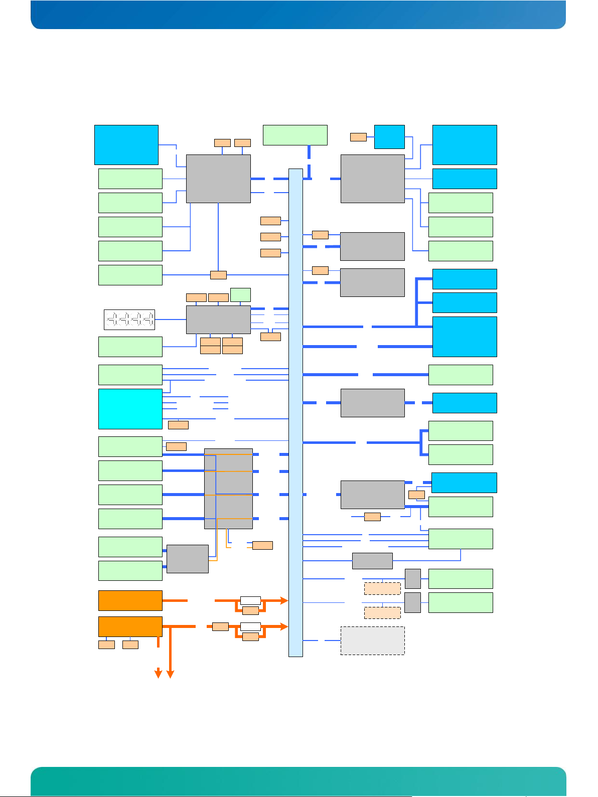
3 Specification
3.1 Functional Specification
» COM Express® COM.0 Rev 2.0 baseboard compatible to Type 10 and Type 1 pin-out based modules
» ATX EPS (20pin + 4pin) power connector
» PLX8112 PCIe2PCI Bridge
» PLX8505 PCIe Switch
» 2 x PCI
» 2 x PCIexpress x16 (electrically x1)
» 1 x PCIexpress x1
» 1 x Express Card
» 2 x SATA
» LVDS (40pin JILI FFC40 connector)
» 1 x DVI-D (SIL1364 SDVOtoDVI)
» 1x Ethernet RJ45
» 6 x USB 2.0/1.1
» 1 x USB Client
» LPC Firmware Hub and SPI Flash support for external BIOS
» Kontron feature connector
» Front panel connectors (HDD Act., Reset and Power Switch)
» Status LED
» SD-Card Socket
» GPIO pin header for module GPIO and Winbond LPC-I/O GPIO
» 4 digit Port 80/81 POST code display with POST code control
» LID and SLEEP support
» Power Control functions (Power Button override, module single supply, power consumption measurements)
» Realtek ALC888/ALC886 HDAudio Codec
- 7.1 Analog Audio Jack
- Optical S/PDIF output
- Digital S/PDIF input/output
- Front Panel HD Audio connector
» Winbond 83627HFJ LPC-I/O
- LPT pin-header
- COM1/COM2 DSUB9 rear panel connector
- PWM FAN and Hardware Monitor connectors (FAN/Voltage)
Page 8
COM Express® Eval Type 10 / Specification
5
CPLD
C
O
N
N
E
C
T
O
R
A
B
SATA#0
(J32)
SATA#1
(J34)
LPT
(J24)
DVI-D
(J68)
Feature
Connector (J37)
Express Card
(J41)
USB #0-3
(J7)
USB #4/6
Ethernet RJ45
(J61)
FrontPanel
Audio (J4)
HWM (FAN)
(J81)
7.1 Analog
Audio Jack
(J8)
LVDS/JILI
(J33)
COM1
COM2
(J9)
S/PDIF in
(J11)
Realtek
ALC888
HD-Audio Codec
Silicon Image
SIL1364
SDVOtoDVI
RS232
BIOS1
LPC FWH
(J74)
SATA
HD Audio
PCIe #1
LVDS
DVI
DDI
SMB
SMB
RST/PWR Control/MISC
GB-LAN
GPIO2
USB #5
RTC
Battery (B1)
SPKR
SPK1
Status LED
J36
J86
24pin ATX
Main Power (J22)
4pin ATX 12V
(J15)
JTAG
(J47)
CTRL
J1
J46
VCC 4.75-14V
R876
LPC
J14
BIOS2
SPI Socket (J76)
SPI Flash optional
SPI
PORT80/81 POST CODE
USB Client #7
(J3)
SD-Card
(J43)
Optical S/PDIF
(J2)
S/PDIF out
(J12)
Winbond
83627
LPC-I/0
LPC
USB
FET Switch
Module GPIO
(J48)
GPIO/SDIO
SDIO
COMA
(J78)
COMB
(J79)
RX0/TX0
RX1/TX1
J60
J75
HWM (Voltages)
(J82)
RST
J85
KBC
PWM FAN1
(J44)
FRU-PROM
I2C EEPROM
(optional)
I2C
MAX
3311
MAX
3311
SER0 (J83)
(optional)
SER1 (J84)
(optional)
GPI0
USB Client
PWRDETECT
J58
I2C
SW3
POST-
SW4
POST+
CPLD GPIO
(J77)
SW5
LID
SW6
SLEEP
LPC
SMB
SW2
RST
SW1
PWR
J40 J42
SIO GPIO
(J72)
Status/Debug
(J80)
LAN LED
SUS_STAT/S3/S4/S5
WDT/TPM/EXCD
Type 1/10 detection
VCC
PCIe Switch status
PCIe x1 SlotC
(J27)
PCIe x16 SlotB
(J26)
PCI Slot 0
(J38)
PCI Slot 1
(J39)
PCIe x16 SlotA
(J25)
PCIe #0
PCIe #3
PCIe #2
enabled
disabled
J62
PLX8505
PCIe
Switch
PEX8112
PCIe2PCI Bridge
Switch
J70
5VSB
R246
J69
PWR CTRL
-12V
3.3V
5V
12V
Baseboard Power
J67
J66
S5ECO
J35
HDD ACT
SW7
RST WDT
HD Audio
(J73)
HD Audio
J71
PWR_OK
J64
J59
3.2 Block Diagram
Page 9
COM Express® Eval Type 10 / Specification
6
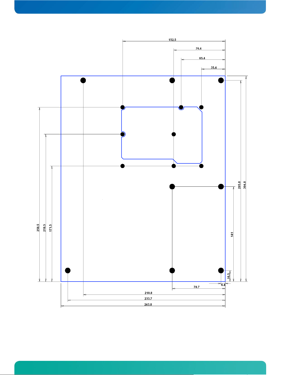
3.3 Mechanical Specification
» Size: 243.8mm x 304.8mm
» max height on top: 34.7mm (Connector J8)
» PCB thickness: 1.4mm ±10%
Page 10
COM Express® Eval Type 10 / Specification
7
Page 11

COM Express® Eval Type 10 / Specification
8
3.4 Electrical Specification
Supply Voltage
» ATX Main Power 24pin
» ATX_12V P4 connector (wide range input depends on module specification)
Power Supply Rise time
» The input voltages shall rise from ≤10% of nominal to within the regulation ranges within 0.1ms to 20ms.
» There must be a smooth and continuous ramp of each DC input voltage from 10% to 90% of its final set-point
following the ATX specification
Supply Voltage Ripple
» Maximum 100 mV peak to peak 0-20MHz
Page 12

COM Express® Eval Type 10 / Specification
9
3.5 Environmental Specification
Ambient temperature
» Operating: 0 to +60 °C
» Non-operating: -30 to +85 °C
Humidity
» Operating: 10% to 90% (non condensing)
» Non operating: 5% to 95% (non condensing)
3.6 MTBF
The following MTBF (Mean Time Between Failures) values were calculated using a combination of manufacturer‟s test
data, if the data was available, and a Bellcore calculation for the remaining parts. The Bellcore calculation used is
“Method 1 Case 1”. In that particular method the components are assumed to be operating at a 50 % stress level in a
40° C ambient environment and the system is assumed to have not been burned in. Manufacturer‟s data has been
used wherever possible. The manufacturer‟s data, when used, is specified at 50° C, so in that sense the following
results are slightly conservative. The MTBF values shown below are for a 40° C in an office or telecommunications
environment. Higher temperatures and other environmental stresses (extreme altitude, vibration, salt water
exposure, etc.) lower MTBF values.
» System MTBF: tbd hours
Page 13
COM Express® Eval Type 10 / Connector Layout
10
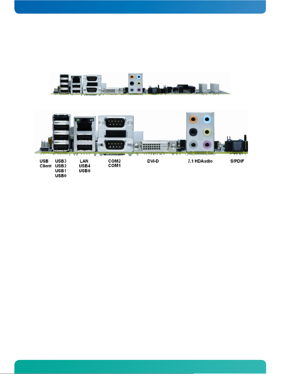
4 Connector Layout
4.1 Rear Panel
Page 14
COM Express® Eval Type 10 / Connector Layout
11
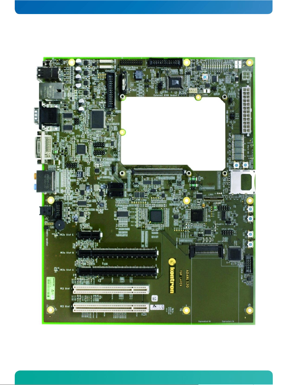
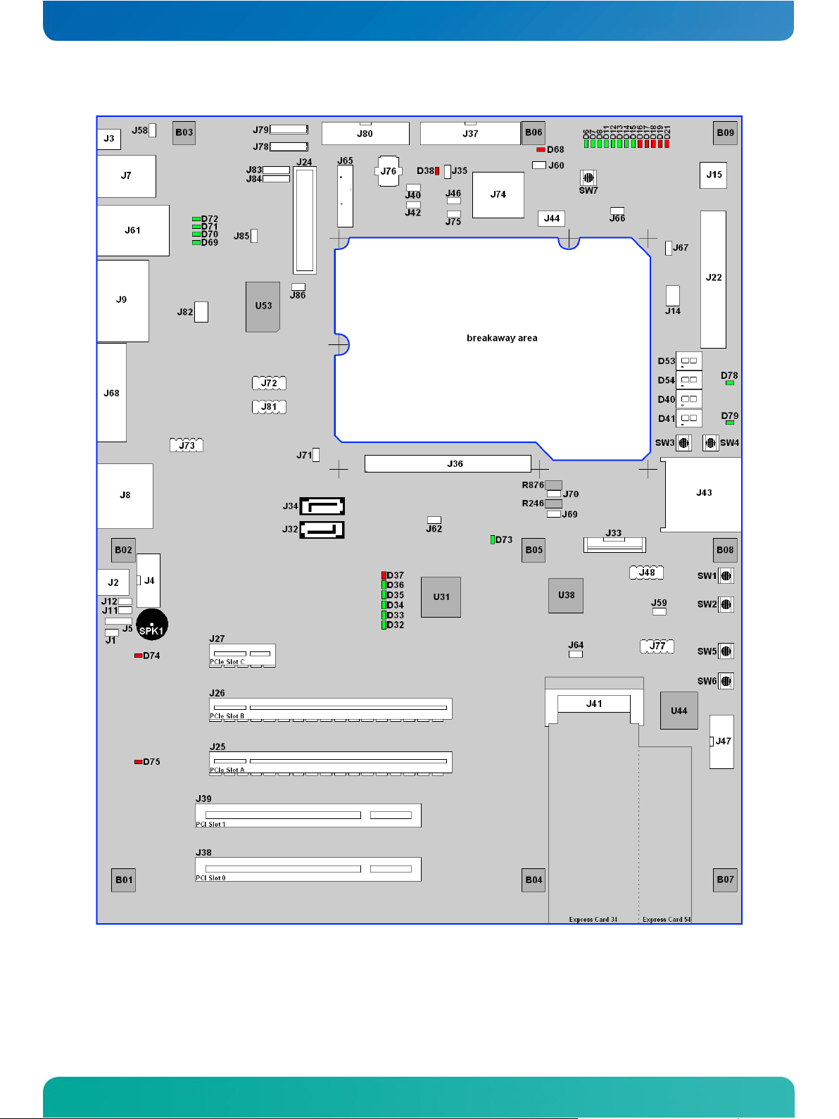
4.2 Connector Locations
Page 15
COM Express® Eval Type 10 / Connector Layout
12
Page 16
COM Express® Eval Type 10 / Connector Layout
13
Connector
Short Description
B01-B09
Baseboard mounting holes
D6
Status LED: VCC 3.3V
D7
Status LED: VCC 5V
D8
Status LED: VCC 5V SBY
D11
Status LED: VCC 12V Module
D12
Status LED: VCC 12V
D13
Status LED: VCC 3.3V SBY
D14
Status LED: VCC 1.0V
D15
Status LED: VCC 1.5V
D16
Status LED: SUS_STAT#
D17
Status LED: SUS_S3#
D18
Status LED: SUS_S4#
D19
Status LED: SUS_S5#
D21
Status LED: THRMTRIP
D32
Status LED: PCIe Switch Lane 4 good (PCIe Slot C)
D33
Status LED: PCIe Switch Lane 3 good (PCIe Slot B)
D34
Status LED: PCIe Switch Lane 2 good (Express Card)
D35
Status LED: PCIe Switch Lane 1 good (PCIe2PCI Bridge)
D36
Status LED: PCIe Switch Lane 0 good (Uplink)
D37
Status LED: PCIe Switch Error
D38
Status LED: HDD activity
D40/41
PORT80 POST code display
D53/54
PORT81 POST code display
D68
Status LED: WDT active
D69
Status LED: GBLAN Activity
D70
Status LED: GBLAN Link
D71
Status LED: GBLAN Link 100
D72
Status LED: GBLAN Link 1000
D73
Status LED: Type10 detection
D74
Status LED: PCIe Switch disabled (PCIe Slot C inactive)
D75
Status LED: PCIe Switch enabled (PCIe Slot A inactive)
D78
Status LED: VCC 1.8V
D79
Status LED: VCC 3.3V for Silicon Image SIL1364
J1
Enable/Disable onboard speaker
J2
Optical S/PDIF out
J3
USB Client connector
J4
Front Panel HDAudio connector
J5
HD Audio GPIO / Digital Microphone
J7
USB #0-3
J8
7.1 Analog Audio Jack
J9
SIO COM1/COM2
J11
S/PDIF input
J12
S/PDIF output
J14
ATX_PS_ON Override
J15
ATX_12V 4pin P4 Power Connector
4.3 Component overview
Page 17

COM Express® Eval Type 10 / Connector Layout
14
J22
ATX 24pin Main Power Connector
J24
LPT
J25
PCIexpress Slot A (x16, electrically x1)
J26
PCIexpress Slot B (x16, electrically x1)
J27
PCIexpress Slot C (x1)
J32
SATA0
J33
LVDS FFC40
J34
SATA1
J35
HDD Activity
J36
COM Express® AB connector for Type1/Type10 Computer-on-Modules
J37
Kontron Feature Connector
J38
PCI Slot0
J39
PCI Slot 1
J40
Power Button Front Panel connector
J41
Express Card
J42
ResetButton Front Panel connector
J43
SD-Card socket
J44
PWM FAN1 (SIO or Module)
J46
Enable external BIOS0 from LPC FWH
J47
CPLD JTAG
J48
Module GPIO
J58
Enable/Disable USB Client Power Detect to GPI0
J59
SDCard/GPIO selection
J60
Enable SIO PWM FAN/Module PWM FAN to FAN1 connector
J61
USB #4 / USB #6 and Ethernet RJ45
J62
Enable/Disable PLX8505 PCIexpress switch
J64
Disable/Enable Express Card
J65
RTC Battery
J66
Disable/Enable S5ECO
J67
Enable/Disable 5V Standby to module
J68
DVI-D (SDVO2DVI)
J69
Module 5VSB measurement point
J70
Module VCC measurement point
J71
Enable/Disable CPLD PWR_OK
J72
SIO GPIO
J73
HDAudio Connector for external codecs
J74
LPC FirmwareHub for external BIOS
J75
Enable external BIOS1 from SPI Flash
J76
SPI Flash for external BIOS
J77
CPLD GPIO
J78
RS232 COMA from module (RX/TX only)
J79
RS232 COMB from module (RX/TX only)
J80
Status/Debug pin-header
J81
SIO HWM: FAN
J82
SIO HWM: Voltages
J83
SER0 from module (RX/TX only)
J84
SER1 from module (RX/TX only)
J85
Enable/Disable SIO KBC
J86
Enable/Disable Winbond LPC-I/O
J92
LID
Page 18

COM Express® Eval Type 10 / Connector Layout
15
SPK1
Speaker
SW1
Power button
SW2
Reset button
SW3
POST Code back
SW4
POST Code foward
SW6
SLEEP
SW7
Reset WDT Latch
U31
PEX8505 PCIe Switch
U38
PLX8112 PCIe2PCI Bridge
U44
Altera CPLD
U53
Winbond 83627 LPC-I/O
Page 19

COM Express® Eval Type 10 / Connectors and Features
16
Pin
ATX Main Power
Pin
ATX Main Power
1 (Orange)
+3.3V
13 (Orange/Brown)
+3.3V / +3.3V sense
2 (Orange)
+3.3V
14 (Blue)
-12V
3 (Black)
GND
15 (Black)
GND
4 (Red)
+5V
16 (Green)
Power on
5 (Black)
GND
17 (Black)
GND
6 (Red)
+5V
18 (Black)
GND
7 (Black)
GND
19 (Black)
GND
8 (Grey)
PWR_OK
20
No connection
9 (Purple)
+5VSB
21 (Red)
+5V
10 (Yellow)
+12V
22 (Red)
+5V
11 (Yellow)
+12V
23 (Red)
+5V
12 (Orange)
+3.3V
24 (Black)
GND Pin
ATX_12V
Pin
ATX_12V
1 (Black)
GND
3 (Yellow)
Module VCC (12V nominal)
2 (Black)
GND
4 (Yellow)
Module VCC (12V nominal)
5 Connectors and Features
5.1 Power supply
5.1.1 ATX connector
The COM Express® Eval Type 10 power supply follows the ATX 2.x specification and the baseboard should be supplied
by connecting an ATX PSU with 24pin ATX and 4pin ATX_12V supply cable in correct orientation. The 4pin ATX_12V
connector mainly supplies power to the module over 0R resistor R876 and allows powering the module directly in
specified wide range power input. The module additionally is supplied with 5V standby voltage over 0R resistor R246.
Standby voltage can easily be disconnected by opening jumper J67 to drive the module in single supply mode. Use
connector J70 and J69 for current measurements.
Page 20

COM Express® Eval Type 10 / Connectors and Features
17
J14 Jumper position
Function
1-2
Power Supply OFF
3-4 (default)
Power Supply controlled by PS_ON signal
5-6
Power Supply always ON
5.1.2 PS_ON override & S5 Eco
With PS_ON override jumper J14 it is possible to switch off the ATX power supply manually. Jumper J66 should be
opened to test module S5Eco or single supply mode.
In S5Eco mode all baseboard components (including status LED) are disconnected from standby voltages in S5 state.
5VSB supply to the module can be disconnected separately with jumper J67.
Note: If S5Eco mode is enabled only power button SW1 is supported to power-on the system.
Page 21

COM Express® Eval Type 10 / Connectors and Features
18
Connector
Function
J40
Power Button
SW1
J42
Reset Button
SW2
5.1.3 Reset and Power button
The COM Express® Eval Type 10 provides an onboard Reset Button (SW1) and Power Button (SW2). To connect a front
panel button from your chassis use J40 (Power) or J42 (Reset).
Page 22

COM Express® Eval Type 10 / Connectors and Features
19
Connector
Function
J92
LID
SW6
Sleep
5.1.4 LID and Sleep
The specification update for PICMG COM.0 modules to revision 2.0 implements new signals for LID and Sleep. The low
active signals can be simulated by switch 5 and 6 similar to notebook functionality of closing the lid or pressing the
sleep button.
Page 23

COM Express® Eval Type 10 / Connectors and Features
20
5.2 COM Express® connector
The COM Express® Eval Type 10 is an evaluation backplane for Type 1 or Type 10 based Computer-on-Modules. Both
types are module pin-outs based on one connectors with 2 rows (Row A and B) with 220 pins overall. Please refer to
your module documentation for detailed pin-out descriptions.
Note: The Type 1 or Type 10 pin-out is compatible to Type 2. It's possible to drive Computer-on-Modules based on
pin-out Type 2 on this evaluation baseboard without functionality of second COM Express® connector CD
(PEG, IDE, PCI).
Page 24

COM Express® Eval Type 10 / Connectors and Features
21
LED
Description
LED
Description
D6
VCC 3.3V
D34
PLX PCIe Switch Lane 2 good (Express Card)
D7
VCC 5V
D35
PLX PCIe Switch Lane 1 good (PCIe2PCI Bridge)
D8
VCC 5V SBY
D36
PLX PCIe Switch Lane 0 good (Uplink)
D11
VCC 12V Module
D37
PLX PCIe Switch Error
D12
VCC 12V
D38
HDD activity
D13
VCC 3.3V SBY
D68
latched WDT
D14
VCC 1.0V
D69
GBLAN Activity
D15
VCC 1.5V
D70
GBLAN Link 10
D16
SUS_STAT#
D71
GBLAN Link 100
D17
SUS_S3#
D72
GBLAN Link 1000
D18
SUS_S4#
D73
Type10 detection
D19
SUS_S5#
D74
PLX PCIe Switch disabled (PCIe Slot C inactive)
D21
THRMTRIP
D75
PLX PCIe Switch enabled (PCIe Slot A inactive)
D32
PLX PCIe Switch Lane 4 good (PCIe Slot C)
D78
VCC 1.8V
D33
PLX PCIe Switch Lane 3 good (PCIe Slot B)
D79
VCC 3.3V for Silicon Image SIL1364
5.3 Status LED
The onboard main status and voltage LED D6-D21 indicates the current power state of the module and if all voltages
are working correctly. Some additional status LED shows active or inactive slots and signals. See table below for
detailed information.
A front panel HDD LED can be connected HDD Activity connector J35. D68 indicates an active watchdog trigger WDT.
The output is buffered and the switch SW7 resets the Latch.
Page 25

COM Express® Eval Type 10 / Connectors and Features
22
SATA Pin
Signal
1
Ground
2
Transmit +
3
Transmit -
4
Ground
5
Receive -
6
Receive +
7
Ground
Connector
SATA Port
J32
SATA #0
J34
SATA #1
5.4 Serial ATA
The COM Express® Type 10 pin-out specification according to COM.0 specification revision 2.0 defines 2 SATA ports.
The COM Express® Eval Type 10 provides two 7-pin SATA data connectors as standard 1.27mm Pitch Serial ATA High
Speed Header with Locking Latch.
Page 26

COM Express® Eval Type 10 / Connectors and Features
23
SD-Card J43 PIN
Description
SD-Card J43 PIN
Description
1
DAT3/CD - Data Line 3/Card Detection
8
DAT1 - Data Line 1
2
CMD - Command/Response
9
DAT2 - Data Line 2
3
VSS 1 - Supply Voltage - GND
10
Card Detect
4
VDD - Supply Voltage - 3.3V
11
Write Protect
5
CLK - Clock
12
COM (GND)
6
VSS2 - Supply Voltage - GND
13
Shield Ground 0
7
DAT0 - Data Line 0
14
Shield Ground 1
GPIO J48 PIN
Description
GPIO J48 Pin
Description
1
VCC 3.3V
2
GPO0 / SD_CLK
3
GPI0 / SD_DATA0
4
GPO1 / SD_CMD
5
GPI1 / SD_DATA1
6
GPO2 / SD_WP
7
GPI2 / SD_DATA2
8
GPO3 / SD_CD#
9
GPI3 / SD_DATA3
10
GND
5.5 SD-Card / Module GPIO
The SD-Card standard is a standard for removable memory storages designed and licensed by the SD Card Association
(http://sdcard.org). The card form factor, electrical interface and protocol are all part of the SD Card specification.
COM Express® Type 1 and Type 10 pin-out based modules may provide a SDIO interface shared with GPIO signals.
Therefore on COM Express® Eval Type 10 a SD-Card connector is available. Please check the documentation of your
module if SDIO is supported and how to enable.
Close configuration jumper J59 (default) to enable SD-Card Slot J43 or open J59 to enable GPIO pin-header J48.
Note1: A SD-Card is detected if Card Detect is at low level. The write protection is active (read only) if SD_WP is at
high level.
Note2: The switching circuitry which selects GPIO or SDIO interface may influence the signal quality of SDIO which
results in detection or boot issues with some fast SD/SDHC cards. Therefore it's recommended to reduce
SDIO interface speed to 24MHz in module's BIOS if supported
Page 27

COM Express® Eval Type 10 / Connectors and Features
24
J8
2-channel
4-channel
6-channel
8-channel
Orange
- - Center/Subwoofer
Center/Subwoofer
Black
-
Rear Speaker
Side Speaker
Rear Speaker Out
Gray - - - Side Speaker Out
Blue
Line In
Line In
Line In
Line In
Green
Line Out
Front Speaker
Front Speaker
Front Speaker
Pink
Mic In
Mic In
Mic In
Mic In
5.6 High Definition Audio
The COM Express® Eval Type 10 provides HDAudio via Realtek ALC888/ALC886 High Definition Audio Codec supporting
analog, optical and digital audio connections.
The onboard buzzer SPK1 can be disabled by opening jumper J1 (default closed). Optical S/PDIF for Toslink
connection is available on rear panel connector J2.
Audio Connector J8 - Speaker Configuration
The Audio Connector J8 on COM Express® Eval Type 10 is a full featured analog audio jack for speaker configuration up
to 8-channel.
Note1: In addition to the default speaker settings, the analog audio Jacks can be reconfigured to perform different
functions via the Realtek HDAudio Driver Software which is available on Kontron website. Only microphones
still must be connected to the default pink jack.
Note2: Audio is only supported with HD Audio compatible COM Express® Modules.
Page 28

COM Express® Eval Type 10 / Connectors and Features
25
Pin
Description
1
MIC2-L
2
GND 3 MIC2-R (MIC Power)
4
PRESENCE#
5
LINE2-R (LineOut-R)
6
MIC2-JD
7
SENSE
8
Key Pin
9
Line2-L (LineOut-L)
10
LINE2-JD
Pin
J5 (HDA GPIO / Dig. MIC)
J11 (S/PDIF in)
J12 (S/PDIF out)
1
HDA_GPIO0 / DMIC-CLK
SPDIF_II
SPDIF_OUT
2
HDA_GPIO1 / DMIC-DATA
GND
GND
3
PWR_3.3V
-
-
4
GND - -
Pin
Description
Pin
Description
1
HDA_BITCLK
2
GND
3
GND 4 HDA_SDIN1
5
HDA_SDIN0_R (default n.c.)
6
HDA_SDIN2
7
GND 8 HDA_SYNC
9
HDA_SDOUT
10
HDA_RST#
Front Panel Audio Connector J4
The front panel audio connector J4 allows connecting a chassis front panel audio with analog microphone input and
stereo speaker output.
Digital Audio Connectors J5/J11/J12
Digital audio inputs and outputs are available on connector J11 (S/PDIF input), J12 (S/PDIF output) and microphone
connection on J5.
Codec connector J73
Connector J73 allows access to HD Audio interface to connect external HDAudio codec additional to the onboard
Realtek ALC888/ALC886.
Page 29

COM Express® Eval Type 10 / Connectors and Features
26
Function
J61 Left LED
J61 Right LED
Status LED
Activity
Green
-
D69
Link10
-
Off
D70
Link100
-
Yellow
D71
Link1000
-
Green
D72
5.7 Ethernet
The COM Express® Eval Type 10 provides a RJ45/Dual USB Combo with a single RJ45 in combination with 2 USB ports
(USB 4/6). Ethernet Connector J61 with integrated magnetics and LED is configured to support modules with Gigabit
Ethernet controller only. Modules with 10/100 MBit Ethernet controller are not supported.
J61 LED function
Page 30

COM Express® Eval Type 10 / Connectors and Features
27
USB Client connectorJ3 - Pin
J3 Function
1
USB Client Power detect
2
USB7-
3
USB7+
4
n.c.
5
GND
6-9
Shield GND
5.8 USB
The COM Express® module's USB ports 0 to 3 are available on rear panel connector J7. USB port 5 is used on Express
Card connector. The COM Express® Eval Type 10 provides USB port 4 and 6 on RJ45/USB Combo connector J61.
Additionally USB7 is available on USB mini-A connector J3 as non-powered connector for USB client functionality.
Check the documentation of your module if USB client on Port #7 is supported and J3 can be used. J58 allows
connecting USB Client Power to GPI0 to use it as detection input for custom USB Client driver software.
Page 31

COM Express® Eval Type 10 / Connectors and Features
28
5.9 PCI
The mini size COM Express® form factor for Type 1 and Type 10 pin-out based modules does not specify an interface for
PCI. Therefore on COM Express® Eval Type 10 a PLX8112 PCIexpress to PCI switch (U38) is used to provide two PCI
Slots following the PCI 2.x specification.
Both PCI slots are enabled when the PCIexpress switch is active. If the PCIe switch is disabled a module with at least 3
PCIexpress lanes is required to enable J38/J39.
Page 32

COM Express® Eval Type 10 / Connectors and Features
29
Computer-on-Module
PCIe switch PEX8505
Connector
PCIe Lane #0
PCIe Lane #0: Uplink
- - PCIe Lane #1
Express Card J41
-
PCIe Lane #2
PCIe2PCI Bridge
-
PCIe Lane #3
PCIe Slot B J26
-
PCIe Lane #4
PCIe Slot C J27
Computer-on-Module
Connector
PCIe Lane #0
PCIe Slot A J25
PCIe Lane #1
Express Card J41
PCIe Lane #2
PCIe2PCI Bridge
PCIe Lane #3
PCIe Slot B J26
5.10 PCIexpress and Express Card
The COM Express® Eval Type 10 provides one PCIexpress x1 port, two PCIexpress x16 ports (electrically x1) and one
Express Card Slot in different configuration. To allow usage of multiple PCIexpress connectors and PCI the PEX8505
PCIexpress switch (U31) is connected to module's PCIexpress Lane #0.
PCIe switch enabled
If PEX8505 PCIe switch is enabled (J62 closed, default) the following routing is active
The PCIexpress Slot A (J25) is disabled in this configuration and marked by red LED D75.
Note: Module PCI Express lanes #1 -#3 are not connected if PCIe switch is enabled
PCIe switch disabled
If PEX8505 PCIe switch is disabled (J62 open) the following routing is active
The PCIexpress Slot C (J27) is disabled in this configuration and marked by red LED D74.
Page 33

COM Express® Eval Type 10 / Connectors and Features
30
LED
Description
D32
PCIe Switch Lane 4 good (PCIe Slot C)
D33
PCIe Switch Lane 3 good (PCIe Slot B)
D34
PCIe Switch Lane 2 good (Express Card)
D35
PCIe Switch Lane 1 good (PCIe2PCI Bridge)
D36
PCIe Switch Lane 0 good (Uplink)
D37
PCIe Switch Error
D74
PCIe Switch disabled (PCIe Slot C inactive)
D75
PCIe Switch enabled (PCIe Slot A inactive)
Pin
J41 Signal
Pin
J41 Signal
1
GND
14
3.3VS_1
2
USB_D-
15
3.3VS_0
3
USB_D+
16
CLKREQ#
4
CPUSB#
17
CPPE#
5
NC
18
REFCLK-
6
NC
19
REFCLK+
7
SMB_CLK
20
GND
8
SMB_DATA
21
PERN0
9
1.5V_2
22
PERP0
10
1.5V_1
23
GND_1
PCIexpress status LED
The PCIexpress status LED D32-D37 shows active devices on available PCIexpress ports and if the PCIe switch is
working correctly
Express Card
The Express Card Slot J41 in combination with USB #5 allows 1.3A on 3.3V, 275mA on AuxPower and 650mA on 1.5V
continuous Card Power with pin-out in table below. Close configuration jumper J64 to disable the Express Card slot
Page 34

COM Express® Eval Type 10 / Connectors and Features
31
Pin
Signal
Level
Signal Description
1
PWR_+5V
5V power
+5V UL-protected with inductor (600R@100MHz, 1A)
2
GPO2
3.3V-O
General-purpose power management event output
3
#BATLOW
3.3V-I
Battery low input. May be driven low by external circuitry to signal that the system
battery is low, or may be used to signal some other external power management
event.
4
GPI2
3.3V-I
General-purpose power management event input
5
#SYS_RESET
3.3V-I
This input may be driven low by external circuitry in order to reset the power
management logic
6
WDT
3.3V-O
Indicating that a Watchdog Timeout Event has occurred (non buffered module
output)
7
LPC_SERIRQ
3.3V-I
Serial interrupt request. This pin is used to support the serial interrupt protocol.
8 - -
Not connected
9
I2C_DAT
3.3V-IO
Data line of I2C-Bus
10
#SMB_ALERT
3.3V-I
System Management Bus Alert input. May be driven low by SMB devices in order to
signal an event on the SM Bus
11
I2C_CLK
3.3V-O
Clock line of I2C-Bus
12
SMB_DAT
3.3V-IO
Clock and data line of SM-Bus.
13
SMB_CLK
3.3V-O
14 - -
Not connected
15
#WAKE1
3.3V-I
Low driven general purpose wake-up signal
16
VCC_RTC
3V-I
3V backup cell input. Should be connected to a 3V backup cell for RTC operation and
storage register non-volatility in the absence of system power. (VBATT = 2.4 – 3.3V)
17
#THRM
3.3V-I
Input from off-module temperature sensor indicating an over temperature situation
18
GND
GND
Ground
19
PWR_OK
3.3V-I
High active input indicating that power from the power supply is ready. It can also
be used as low active reset input signal.
20
GND
GND
Ground
21
#PWRBTN
3.3V-I
Power Button Input. This input is used to support the ACPI Power Button function.
5.11 Kontron Feature connector
The Kontron Feature connector provides additional interfaces such as I2C, SMBus or Power Control Signals. See the
table below for detailed pin-out description
Page 35

COM Express® Eval Type 10 / Connectors and Features
32
22
GND
GND
Ground
23
#ATA_ACT
3.3V-O
Low active output signal, which indicates activity on IDE interfaces.
24
#CB_RESET
3.3V-O
Low active Reset output from module to carrier board
Page 36

COM Express® Eval Type 10 / Connectors and Features
33
5.12 DVI-D
On COM Express® Eval Type 10 the DVI output is available through a Silicon Image SiL1364/A SDVO to single link DVI
PanelLink Transmitter. Check your module documentation if SDVO is available on DDI interface defined for Type 10
pin-out based modules.
Page 37

COM Express® Eval Type 10 / Connectors and Features
34
Pin
LVDS Signal
Pin
LVDS Signal
1
NC
21
LCDDO13
2
LCDDO0
22
DETECT# (GND)
3
LCDDO1
23
LCDDO14
4
ENAVDD
24
LCDDO15
5
LCDDO2
25
GND
6
LCDDO3
26
LCDDO16
7
NC
27
LCDDO17
8
LCDDO4
28
GND 9 LCDDO5
29
LCDDO18
10
GND
30
LCDDO19
11
LCDDO6
31
+5V
12
LCDDO7
32
+5V
13
GND
33
+5V
14
LCDDO8
34
+5V
15
LCDDO9
35
BLON#
16
JILI_DAT
36
GND
17
LCDDO10
37
GND
18
LCDDO11
38
+12V
19
JILI_CLK
39
+12V
20
LCDDO12
40
+12V
5.13 LVDS
The 40-pin JILI LVDS panel connector J33 allows connecting a flat panel directly to the module's dual channel LVDS
output. Check your module documentation for available BIOS configurations for this flat panel output.
Page 38

COM Express® Eval Type 10 / Connectors and Features
35
5.14 External BIOS
The COM Express® Eval Type 10 supports external boot. By closing Jumper J46 the module's onboard BIOS is disabled
and the system will boot from an external Firmware Hub in U43 PLCC socket J74.
For modules supporting SPI boot the COM Express® Eval Type 10 provides a SPI socket J76 for an optional available
SPI Flash. SPI is part of COM.0 Specification Rev 2.0 and external SPI boot can be enabled by closing Jumper J75.
Please check the documentation of your module if SPI is supported and which SPI Flash size is required.
Booting from external BIOS:
» Close Jumper J46 to boot from the baseboard's LPC Firmware
» Close Jumper J75 to boot from the baseboard's SPI Flash
Flashing the external BIOS:
» Prepare a bootable USB flash drive and save BIOS and flash utility in the root folder
Please check Application Note KEMAP046 avialble at Kontron's customer section for more details
» Open J46/J75 to boot from the module's BIOS
» Power on the system and boot from our USB flash drive
» Close J46 to enable the LPC FWH or close J75 to enable the SPI Flash
» Execute the BIOS update command (e.g. afudos.exe bios.rom /P /B /N /C /X)
» Reboot your system if flash procedure has finished
» Your system should now start from external BIOS
Note: Please check module documentation if external boot from LPC FWH and/or SPI Flash is supported
Warning: Do not close both jumpers at the same time
Page 39

COM Express® Eval Type 10 / Connectors and Features
36
Pin
J78 (COMA)
J79 (COMB)
J83 (SER0, A98/99)
J84 (SER1, A101/102)
1
n.c.
n.c.
+5V
+5V 2 n.c.
n.c.
SER0_TX
SER1_TX
3
RX0
RX1
SER0_RX
SER1_RX
4
n.c.
n.c.
GND
GND 5 TX0
TX1 - -
6
n.c.
n.c. - -
7
n.c.
n.c. - - 8 n.c.
n.c. - -
9
GND
GND - -
10
+5V
+5V - -
5.15 Serial Interface
The PICMG COM.0 specification revision 2.0 defines two optional 2-pin serial interfaces on COM Express® connector
pins A98/A99 and A101/A102 formerly used for 12V VCC input. Both new interfaces are available directly on optional
pin-header J83 and J84.
J78 and J79 allow both interfaces to be used as 2-pin RS232 interfaces COMA and COMB with Kontron Adapter cable
KAB-DSUB9-3. Please check the documentation of your module if this interface is supported and how to configure.
Page 40

COM Express® Eval Type 10 / Connectors and Features
37
Pin
Description
Pin
Description
1
+3.3V SBY
2
GND
3
TPM_PP
4
SUS_STAT#
5
WDT_LATCHED
6
SUS_S3#
7
RST_WDT_L#
8
SUS_S4#
9
SPKR
10
SUS_S5#
11
EXCD0_CPPE#
12
GBE0_ACT#
13
EXCD0_PERST#
14
GBE0_LINK100#
15
EXCD1_CPPE#
16
GBE0_LINK1000#
17
EXCD1_PERST#
18
GBE0_LINK#
19
+3.3V
20
GND
5.16 Status & Debug Connector
For debugging and measurements some important status signals are available on pin-header J80 for direct access.
Page 41

COM Express® Eval Type 10 / Connectors and Features
38
5.17 CPLD & POST-Code Display
Power Management control, 4 digits LPC/PCI Port 80/81 Post Code and additional GPIOs are implemented in onboard
Altera CPLD (U44).
Port 80/81 POST Code display
The 7-segment display D53/D54 for Port 81 and D40/41 for Port 80 shows BIOS status codes during boot-up process.
Last 8 check codes are stored automatically and can be controlled by switch SW3 (Post Code step backward) and
switch SW4 (Post code step forward). Pressing SW3 and SW4 simultaneously returns to newest POST code.
The POST Code display also shows current Suspend state:
» S3 -> POST code "_ _ _ 3"
» S4 -> POST code "_ _ _ 4"
» S5 -> POST code "_ _ _ 5"
Power Good J71
The Power Good output generated by the CPLD must be high level to allow the module to start. Some modules may
provide direct power-on support if VCC gets connected and PWR_OK (COM Exress pin B24) is open or at high level. To
test this functionality configuration jumper J71 can be opened to disconnect Power Good.
Page 42

COM Express® Eval Type 10 / Connectors and Features
39
J7 pin
Function
J7 pin
Function
1
VCC 3.3V SBY
2
GND
3
CPLD_IO_PIN64
4
CPLD_IO_PIN66
5
CPLD_IO_PIN67
6
CPLD_IO_PIN68
7
CPLD_IO_PIN69
8
CPLD_IO_PIN70
9
CPLD_IO_PIN71
10
CPLD_IO_PIN72
J7 pin
Function
J7 pin
Function
1
TCK (PD 1K0)
2
GND
3
TDO (PU 1K0 3.3VSBY)
4
3.3V SBY
5
TMS (PU 1K0 3.3VSBY)
6
n.c. 7 n.c. 8 n.c.
9
TDI (PU 1K0 3.3VSBY)
10
GND
J77 - CPLD I/O Port
The I/O Port J77 provides 8 I/O ports directly from the CPLD without any functionality in default configuration.
J47 - CPLD JTAG Connector
Page 43

COM Express® Eval Type 10 / Connectors and Features
40
5.18 Winbond 83627 Super-I/O
A Winbond 83627HFJ Super-I/O controller (U53) is connected to module's LPC bus to offer legacy interfaces like
RS232 and parallel ports additionally to temperature, FAN and voltage monitoring features. The default SIO LPC
address is 2Eh.
The configuration jumpers J85 enables the SIO keyboard controller when closed. Open J86 to hold the Super-I/O in
reset to simulate a legacy free backplane.
Note: A LPC Super-I/O controller requires BIOS support. Please check the documentation of your module if the
Winbond 83627 is supported.
Page 44

COM Express® Eval Type 10 / Connectors and Features
41
Pin
Signal
1
DCD 2 RX
3
TX
4
DTR 5 GND
6
DSR
7
RTS 8 CTS
9
RI
5.18.1 RS232
With Winbond 83627 LPC-I/O two serial ports are supported. Both COM ports can be configured in module BIOS setup
if Super-I/O support is implemented.
Page 45

COM Express® Eval Type 10 / Connectors and Features
42
Pin
Signal
Pin
Signal
1
#STB 2 #AFD 3 PD0 4 #ERROR
5
PD1 6 #INIT
7
PD2 8 #SLCTIN
9
PD3
10
GND
11
PD4
12
GND
13
PD5
14
GND
15
PD6
16
GND
17
PD7
18
GND
19
#ACK
20
GND
21
BUSY
22
GND
23
PE
24
GND
25
SLCT
26
n.c.
5.18.2 LPT
The Winbond 83627 LPC-I/O supports one parallel port available on baseboard's pin header J24. Use the optional
available KAB-DSUB25-1 cable adapter to access the LPT port and check to module BIOS to configure the port
resources.
Page 46

COM Express® Eval Type 10 / Connectors and Features
43
Pin
J50 on COM Express® Eval Type 10
1
GND 2 +12V
3
Sense
4
Control (PWM)
5.18.3 FAN
The COM Express® Eval Type 10 provides one 4-pin PWM FAN connector directly controlled by the LPC-I/O PWM output
1. If configuration jumper J60 is open (default) the PWM FAN J44 is controlled by the module FAN output specified in
COM.0 revision 2.0 specification if supported by the module.
Page 47

COM Express® Eval Type 10 / Connectors and Features
44
Pin
J72 - GPIO
J81 - FAN
J82 - Voltage
1
+5V
+3.3V
SIO HWM IN - VCOREA
2
GND
GND
SIO HWM IN - 12V
3
SIO GP10 / JOAYABTN0
Module FAN_PWMOUT#
SIO HWM IN - VCOREB
4
SIO GP11 / JOYBBTN0
Module FAN_TACHIN
SIO HWM IN - -5V
5
SIO GP12 / JOYAX
SIO HWM OUT - FANPWM1
SIO HWM IN - 3.3V
6
SIO GP13 / JOYBX
SIO HWM IN - FANIO1
GND 7 SIO GP14 / JOYBY
SIO HWM OUT - FANPWM2
-
8
SIO GP15 / JOYAY
SIO HWM IN - FANIO2
-
9
SIO GP16 / JOYBBTN1
SIO GP20 / MDRX
SIO HWM OUT - FANPWM3
-
10
SIO GP17 / JOYABTN1
SIO IRQIN / MDTX0
SIO HWM IN - FANIO3
-
5.18.4 SIO Debug connectors
For debugging Winbond 83627 LPC-I/O GPIOs and FAN/Voltage interfaces are available via pin-header.
Note: Check the module's BIOS how to enable the baseboard hardware monitor for monitoring voltages and fan
SIO GPIOs are not accessible via JIDA interface.
revolutions via JIDA32/K-Station or in BIOS HWM setup page.
Page 48

COM Express® Eval Type 10 / Connectors and Features
45
Chip
SM Bus Address
Clock Buffer IDT ICS9DB801C
0x6e/0xdc
PCIe switch PLX PEX 8505AA
0x3f/0x7e
5.19 FRU-PROM (I2C EEPROM)
Following the new COM Express® specification the COM Express® Eval Type 10 provides an I2C EEPROM. The FRU-PROM
(Field Replacable Unit; U76) at I2C address 07h can be used to store user specific data or baseboard configuration
settings.
5.20 SM Bus Devices
The COM Express® Evaluation Board Type 10 uses 2 chips that are connected to the SM Bus of the module at the
following addresses:
Page 49

COM Express® Eval Type 10 / Battery Information
46
6 Battery Information
English:
CAUTION: Danger of explosion if battery is incorrectly replaced. Replace only with the same or equivalent type
recommended by the manufacturer. Dispose of used batteries according to the manufacturer‟s
instructions.
Deutsch:
VORSICHT: Explosionsgefahr bei unsachgemäßem Austausch der Batterie. Ersatz nur durch denselben oder
einen vom Hersteller empfohlenen gleichwertigen Typ. Entsorgung gebrauchter Batterien nach
Angaben des Herstellers.
French:
ATTENTION: Risque d„explosion avec l„échange inadéquat de la batterie. Remplacement seulement par le même
ou un type équivalent recommandé par le producteur. L‟évacuation des batteries usagées
conformément à des indications du fabricant.
Danish:
ADVARSEL: Lithiumbatteri – Eksplosionsfare ved fejlagtig Håndtering. Udskifting må kun ske med batteri af
samme fabrikant og type. Lever det brugte batteri tilbage til leverand
Page 50

COM Express® Eval Type 10 / Battery Information
47
Finnish:
VAROITUS: Paristo voi rãjãhtãã, jos se on virheellisesti asennettu. Vaihda paristo ainoastaanlaltevalmistajan
suosittelmaan tyyppiln. Havita kaytetty paristo valmistajan ohjeiden mukaisesti.
Spanish:
Precaución: Peligro de explosión si la batería se sustituye incorrectamente. Sustituya solamente por el mismo o
tipo equivalente recomendado por el fabricante. Disponga las baterías usadas según las
instrucciones del fabricante.
Note: The battery of this product is not considered to be accessible by the end user. Therefore the safety
instructions are only given in English, German, French, Danish, Finish and Spanish language.
If the battery of this product however is accessible by the end user, it is in the responsibility of the
Kontron customer to give the corresponding safety instructions in the required language(s).
Page 51

COM Express® Eval Type 10 / Module Single Supply and Wide Range
48
7 Module Single Supply and Wide Range
The Computer-on-Module power is supplied directly from ATX_12V connector J15. Kontron modules are capable of
working in a wide range voltage input and therefore it's possible to connect module VCC on J15 parallel to ATX supply
J22 for the baseboard.
Please check the documentation of your product if a wide range voltage input is supported. Kontron Computer-onModules usually supports:
» COM Express® modules in mini size form factor:
4.75V to 14V
» COM Express® modules in compact and basic size form factor
8.5V to 18V
Additionally Kontron modules support single supply operation without standby voltage. To enable module single
supply mode open jumper:
» J66 to enable Baseboard's S5Eco mode
» J67 to disconnect 5VSB from the module
» J71 to disconnect Power Good (PWR_OK)
Page 52

COM Express® Eval Type 10 / Compatibility Matrix
49
Con
Feature
COMe-mSP1
COMe-mTT10
COMe-mCT10
J15
ATX 12V Power
4.75V - 14V
4.75V - 14V
4,75-14V
J25
PCIexpress Slot A
if PCIe Switch is disabled
if PCIe Switch is disabled
if PCIe Switch is disabled
J26
PCIexpress Slot B
if PCIe Switch is enabled
if PCIe Switch is enabled
if PCIe Switch is enabled
J27
PCIexpress Slot C
if PCIe Switch is disabled
if PCIe Switch is disabled
if PCIe Switch is disabled
J41
ExpressCard
YES, but USB#5 is USB 2.0 only
YES
YES
J38
PCI Slot0
if PCIe Switch is enabled
YES
if PCIe Switch is disabled
J39
PCI Slot 1
if PCIe Switch is enabled
YES
if PCIe Switch is enabled
J41
Express Card
if PCIe Switch is enabled
YES
if PCIe Switch is disabled
J34
SATA1
on variants without onboard LAN
YES
YES
J61
USB #4 / USB #6
Ethernet RJ45
USB 2.0 only
No USB #6
YES
J44
PWM FAN (SIO/Module)
SIO YES / Modoule NO
SIO YES / Module optional
SIO YES / Module YES
J68
DVI-D (SDVO2DVI)
Optional
YES
NO
J74
LPC FWH for external BIOS
YES
NO
NO
J76
SPI Flash for external BIOS
NO
YES
YES
J78
RS232 COMA from module
NO
YES
Optional
J79
RS232 COMB from module
NO
YES
Optional
J83
SER0 from module
NO
YES
Optional
J84
SER1 from module
NO
YES
Optional
J92
LID
NO
Optional
YES
SW6
SLEEP
NO
Optional
YES
8 Compatibility Matrix
The COM Express® Eval Type 10 supports Computer-on-Modules following PICMG COM.0 Revision 1.0 pin-out Type 1 or
COM.0 revision 2.0 pin-out Type 10.
See table below wich features are supported by Kontron's COM Express® mini form factor modules:
Page 53

COM Express® Eval Type 10 / Power Distribution
50
9 Power Distribution
Page 54

COM Express® Eval Type 10 / Security Advice
51
10 Security Advice
To protect the external power lines to peripheral devices the customer has to take care about:
- The wires to the external device have the right diameter to withstand the max. available current
- The housing of the external device fulfils the fire protection requirements of IEC/EN 60950.
Page 55

COM Express® Eval Type 10 / Document Revision History
52
Revision
Date
Edited by
Changes
0.10_prelim
08.10.08
PRO
Initial Release for nanoETXexpress Eval Board COM.0 revision 1.0 Type 1
110
11.10.2010
PRO
Updated to redesign variant 34101-0000-00-1
nanoETXexpress Eval Board COM.0 revision 2.0 Type 1/Type 10
120
04.11.2010
PRO
Added speed limitation for SDIO
Updated supported features by nETXe-SP
130
04.11.2010
PRO
Updated Product name
140
13.07.2011
UMA
Updated ® and ™, changed LID button to LID jumper, changed “ALC888” to
“ALC888/ALC886”, added SM Bus addresses
141
07.03.2011
UMA
Renaming from ETXexpress® to COM Express® an ultra to mini, removed typo at
KAB-DSUB9-3
Europe, Middle East & Africa
Oskar-von-Miller-Str. 1
85386 Eching/Munich
Germany
Tel.: +49 (0)8165/ 77 777
Fax: +49 (0)8165/ 77 219
info@kontron.com
North America
14118 Stowe Drive
Poway, CA 92064-7147
USA
Tel.: +1 888 294 4558
Fax: +1 858 677 0898
info@us.kontron.com
Asia Pacific
17 Building,Block #1,ABP.
188 Southern West 4th Ring
Beijing 100070, P.R.China
Tel.: + 86 10 63751188
Fax: + 86 10 83682438
info@kontron.cn
11 Document Revision History
Corporate Offices
 Loading...