

Page 1
» Quick Start Guide «
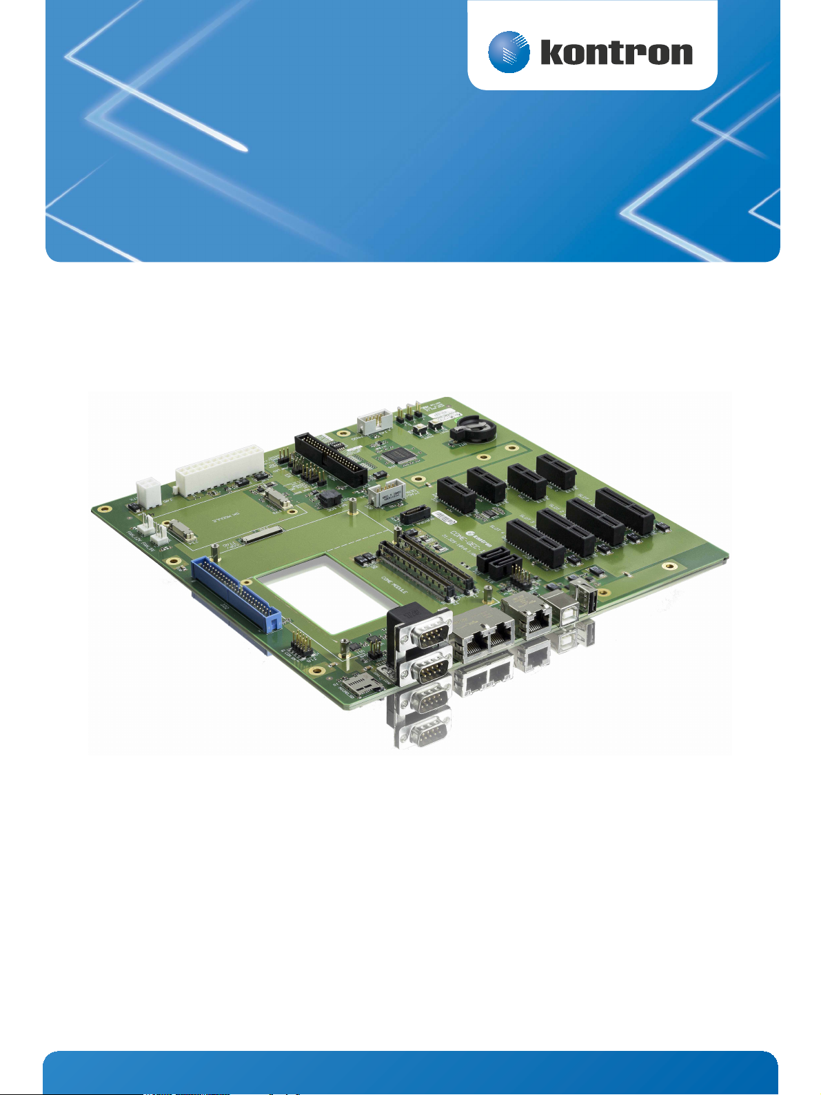
COME-QEC-1
Doc. ID: 1054-1776, Rev. 1.0
Date: March 5, 2013
The pulse of innovation
Page 2
Quick Start Guide
Revision History
Publication Title: COME-QEC-1 “COM Express® QorIQ™ Evaluation Carrier 1” Quick Start Guide
Doc. ID: 1054-1776
Rev. Brief Description of Changes Date of Issue
1.0 Initial issue 5-Mar-2013
COME-QEC-1
Imprint
Kontron Europe GmbH may be contacted via the following:
MAILING ADDRESS TELEPHONE AND E-MAIL
Kontron Europe GmbH +49 (0) 800-SALESKONTRON
Sudetenstraße 7 sales@kontron.com
D - 87600 Kaufbeuren Germany
For further information about other Kontron products, please visit our Internet web site: www.kontron.com.
Disclaimer
Copyright © 2013 Kontron AG. All rights reserved. All data is for information purposes only and not guaranteed for legal purposes. Information has been carefully checked and is believed to be accurate; however, no responsibility is assumed for inaccuracies. Kontron and the Kontron logo and all other trademarks or registered trademarks are the property of their respective
owners and are recognized. Specifications are subject to change without notice.
2
www.kontron.com
Page 3

Quick Start Guide
COME-QEC-1
CONTENTS
1 Scope ................................................................................................................................ 5
2 Safety ............................................................................................................................... 5
3 Getting Started ................................................................................................................... 5
3.1 How to Configure the Cables and the Host PC Terminal Software Client for Basic Startup ........................ 5
3.2 Additional Configurations ...................................................................................................... 5
4 Functional Block Diagram ....................................................................................................... 6
5 COME-QEC-1 Board Layout and Connectors .................................................................................. 7
5.1 Board Layout ...................................................................................................................... 7
5.2 Connectors ......................................................................................................................... 7
5.2.1 COM Express® Module Connector Connectors J1 and J2 .................................................................. 9
5.2.2 USB Connectors J3/J4/J14 ................................................................................................... 15
5.2.3 Ethernet Connectors J5/J6L/J6R ........................................................................................... 15
5.2.4 Serial Interface Connectors J7 Upper and Lower ........................................................................ 15
5.2.5 microSD/SDHC Card Connector J8 ........................................................................................... 15
5.2.6 IEEE-1588 Sideband Signal Connector J9 ................................................................................. 16
5.2.7 SATA Connectors J15/J21 ..................................................................................................... 16
5.2.8 SLOT 1 Connector J17 .......................................................................................................... 17
5.2.9 SLOT 2 Connector J18 .......................................................................................................... 19
5.2.10 SLOT 3 Connector J19 .......................................................................................................... 21
5.2.11 SLOT 4 Connector J20 .......................................................................................................... 23
5.2.12 Local Bus / GPIO connector J22 ............................................................................................. 25
5.2.13 SLOT 1 Sideband Connector J23 ............................................................................................. 26
5.2.14 SLOT 2 Sideband Connector J24 ............................................................................................. 27
5.2.15 SLOT 3 Sideband Connector J25 ............................................................................................. 28
5.2.16 SLOT 4 Sideband Connector J26 ............................................................................................. 29
5.2.17 SPI-Flash Socket J31 ........................................................................................................... 29
5.2.18 FAN Connectors J35 and J36 ................................................................................................. 29
5.2.19 Miscellaneous Signal Connector J37 ....................................................................................... 30
5.2.20 I2C/SM-Bus Evaluation Header J38 ......................................................................................... 30
5.2.21 Board Power Supply Connectors J44 and J45 ............................................................................. 31
5.2.22 BT1 RTC Backup Battery Socket .............................................................................................. 31
6 Jumpers .......................................................................................................................... 32
7 Switches .......................................................................................................................... 33
7.1 DIP Switch SW3 .................................................................................................................. 33
7.2 Other Switches .................................................................................................................. 33
7.2.1 Reset Switch (Push Button Switch SW1) ................................................................................... 33
7.2.2 Power Switch (Push Button Switch SW2) .................................................................................. 33
8 Onboard EEPROM ................................................................................................................ 33
9 Adapter Cards ................................................................................................................... 34
9.1 Adapter Card ADAP-EVAL-QORIQ-SGMII .................................................................................... 34
9.2 Adapter Card ADAP-EVAL-QORIQ-XAUI ..................................................................................... 35
9.2.1 PHY Infrastructure and Operation ........................................................................................... 36
9.2.2 DIP Switches ..................................................................................................................... 36
9.2.2.1 SFP+ Rate Select DIP Switch SW1 ............................................................................................ 36
9.2.2.2 EEPROM Configuration DIP Switch SW2 ..................................................................................... 37
3
www.kontron.com
Page 4

Quick Start Guide
COME-QEC-1
9.2.3 Configuration ................................................................................................................... 37
9.2.4 Enable LEDs ...................................................................................................................... 37
9.3 Adapter Card ADAP-EVAL-QORIQ-SRIO ...................................................................................... 37
TABLES
1 COME-QEC-1 Connector Overview ............................................................................................... 8
2 Connector J1 Rows A and B Pinout ............................................................................................. 9
3 Connector J2 Rows C and D Pinout ............................................................................................12
4 D-SUB9 Serial UART Connectors J7 (Upper and Lower) Pinout ..........................................................15
5 IEEE-1588 Sideband Signal Connector J9 Pinout ..........................................................................16
6 SLOT 1 Connector J17 Pinout ...................................................................................................17
7 SLOT 2 Connector J18 Pinout ...................................................................................................19
8 SLOT 3 Connector J19 Pinout ...................................................................................................21
9 SLOT 4 Connector J20 Pinout ...................................................................................................23
10 Local Bus/GPIO Connector Pinout J22 .......................................................................................25
11 SLOT 1 Sideband Connector J23 Pinout ......................................................................................26
12 SLOT 2 Sideband Connector J24 Pinout ......................................................................................27
13 SLOT 3 Sideband Connector J25 Pinout ......................................................................................28
14 SLOT 4 Sideband Connector J26 Pinout ......................................................................................29
15 Miscellaneous Signal Connector J37 Pinout ................................................................................30
16 I2C/SM-Bus Connector J38 Pinout ............................................................................................30
17 ATX Main Power J44 Pinout .....................................................................................................31
18 ATX 12V J45 Pinout ...............................................................................................................31
19 COME-QEC-1 Jumpers Overview ................................................................................................32
20 DIP Switch SW3 Configuration .................................................................................................33
21 LED 1: Link/Activity ..............................................................................................................34
22 LED 2: Speed .......................................................................................................................34
23 Port Configuration ...............................................................................................................35
24 LED0 .................................................................................................................................36
25 LED1 .................................................................................................................................36
26 SFP+ Rate Select DIP Switch SW1 Configuration ...........................................................................36
27 EEPROM Configuration DIP Switch SW2 .......................................................................................37
FIGURES
1 COME-QEC-1 Functional Block Diagram ...................................................................................... 6
2 Board Layout ...................................................................................................................... 7
3 Functional Block Diagram of the ADAP-EVAL-QORIQ-SGMII Adapter Card ........................................... 34
4 Port Assignment Front View .................................................................................................. 35
5 Functional Block Diagram of the ADAP-EVAL-QORIQ-XAUI Adapter Card ............................................ 35
6 ADAP-EVAL-QORIQ-XAUI Adapter Card LED and DIP Switch Locations ............................................... 36
7 Functional Block Diagram of the ADAP-EVAL-QORIQ-SRIO Adapter Card ............................................ 37
4
www.kontron.com
Page 5

Quick Start Guide
COME-QEC-1
1 Scope
The COME-QEC-1 COM Express® Evaluation microATX carrier board for Kontron’s COMe-bP5020 and COMe-cP2020 COM Express®
QorIQ™ modules is designed to allow embedded application developers to quickly get their application up and running and to
verify the basic operation of the Freescale™ QorIQ™ processors P5020 and P2020, giving them a head start on the total system
design. The focus of this document is to describe how to successfully connect to the COME-QEC-1, how to make the initial setup
for both processor modules in order to evaluate the performance of the processor modules, their IO-capability or just to begin
software development.
For technical information concerning the COM Express® modules, refer to their respective user guides (available on the
Kontron Web Site).
2 Safety
1. This guide assumes that personnel involved in the handling and operation of this product are technically competent and
cognizant of safety requirements for the usage of such products. For further information concerning product safety refer to the
respective product user guides.
2. Handling and operation of this product requires observance of ESD precautions.
3. Kontron disclaims any and all responsibilities for damage resulting from use by unskilled personnel or failure to apply ESD
safety measures.
3 Getting Started
3.1 How to Configure the Cables and the Host PC Terminal Software Client for Basic Startup
For a proper startup of the COM Express® QorIQ™ evaluation packages it is necessary to provide correct power to the system
and a serial connection to a host PC in order to configure the functionality of the required interfaces.
1. If required, install adapter card(s) and a COM Express® QorIQ™ module
2. Ensure that an ATX power supply is connected to the ATX power connectors
3. Ensure that an RS232 Null-Modem cable is connected to the lower D-Sub9 serial connector (COM0) and the host PC
4. The host PC's serial port must be configured as follows:
» Data rate: 115200 bps
» Number of data bits: 8
» Parity: None
» Number of Stop bits: 1
» Hardware Flow Control: None
5. Push the Power Button to startup the COM Express® QorIQ™ evaluation package
6. U-Boot starts
Once the U-Boot prompt appears on the host PC, the operator has access to the COM Express® QorIQ™ module
3.2 Additional Configurations
After the command prompt is displayed, the main interfaces may be configured using the Kontron U-Boot SCONF mechanism.
For further information about these possibilities please refer to the appropriate user guide for the module being evaluated.
5
www.kontron.com
Page 6
Quick Start Guide
COM-Express Connectors
Bank1 A-D
Bank1 E-H
Bank2 A-D
MDI
1x SD/SDHC Card I/F
Local Bus, 2x DMA
SATA Cable Connectors
ETHMagJack
sRIO x4 adapter card (S0012)
or PCIe x4 adapter card (standard)
SLOT 1
SLOT 2
SLOT 3
SLOT 3
Sideband
4x 1GbE (SGMII) adapter card (S0010)
or 1x 10GbE (XAUI) adapter card (S0011)
RS232/422
RS232/422
Serial
Serial
D-SUB 9
D-SUB 9
MDIO/MDC
COME module site
COME carrier site
P5020 SERDES
Mapping
RxD/TxD/RTS/CTS
RxD/TxD/RTS/CTS
SLOT 4
SLOT 4
Sideband
1x 10GbE (XAUI) adapter card (S0011)
SERDES 0-3
SERDES 4-7
SERDES 10-13
SERDES 14-17
ETH
ETH
Dual
MagJack
Carrier USB
Header Connector
USB
USB Type B Device
or Type A Host
USB
USB
SATA
SATA
P2020 SERDES
Mapping
JTAG, Debug
2x I2C, 1x SPI
12V
ATX Power Conn.
3.3V / 5V / 12V
5V STDBY
Header
Header
Header
IEEE1588
microSDHC
Card
MDI
4x USB
1x USB
N.A.
N.A.
PWR
Bank3 A-D
SATA 0,1
UART 0
UART 1
SDHC
dTSEC 5
JTAG, Debug
IEEE1588
2x I2C, 1x SPI
IRQ[5:1]#, IRQ_OUT#, ...
USB 2
USB 1 (Hub)
microSD/SDHC
Card Socket
MDIO/MDC
Fan
12V
Bank1 A-D
eTSEC 3
eTSEC 2
UART 0
UART 1
SDHC
eTSEC 1
JTAG, Debug
IEEE1588
2x I2C, 1x SPI
N.A.
USB 1 (Hub)
EC MDIO/MDC
SLOT 1
Sideband
SLOT 2
Sideband
Header
IRQ[5:1]#, IRQ_OUT#, ...
EXP Card
EXP Card signals
1x USB
1x USB
2x USB
Sideband Connectors
22 Pin Aurora
Debug Connector
SERDES 8-9
Bank1 I-J N.A.
MDI
5V STDBY
sRIO x4 adapter card (S0012)
or PCIe x4 adapter card (standard)
USB
Fan
5V
SPI-Socket
LA[31:16], LAD[15:0], LCS[0:1]#, LALE, LCTL, LGTA,
LOE#, LWE[0:1]#, DMAx_REQ/ACK/DONE#
CPLDLEDs
RST B.
DIP SW
Header
IRQ, MISC
X
I2C EEPROM
MUX
MUX
COME-QEC-1
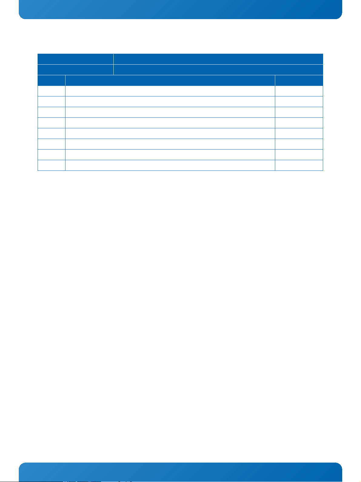
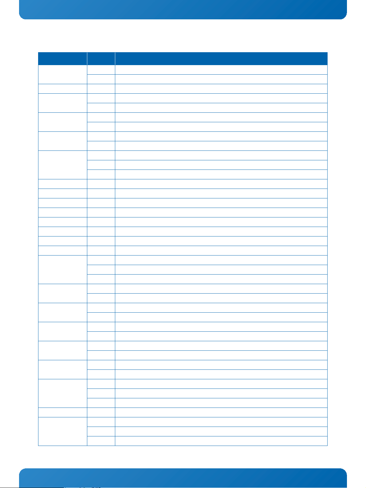
4 Functional Block Diagram
The following figure illustrates the interfacing available on the COME-QEC-1 for both the COMe-cP2020 and the COMe-bP5020
COM Express® modules.
Figure 1: COME-QEC-1 Functional Block Diagram
6
www.kontron.com
Page 7
Quick Start Guide
µSD
COM1
COM0
GBE2
GBE1
GBE0
USB/D
USB/H
J8
J7
J6
J5
J4
J3
J13
J12
J11
J10
J16
129
10
J22
1
2
49
50
J2
J1
J9
12
11 12
J14
1
210
7
J21J15
SATA0 SATA1
USB
A1
A32
B1 B32
J20
A1
A32
B1 B32
J19
A1
A32
B1 B32
J18
A1
A32
B1 B32
J17
SLOT 4 MAIN
SLOT 3 MAIN
SLOT 2 MAIN
SLOT 1 MAIN
A1
A18
B1 B18
J26
SLOT 4 SB
A1
A18
B1 B18
J25
SLOT 3 SB
A1
A18
B1 B18
J24
SLOT 2 SB
A1
A18
B1 B18
J23
SLOT 1 SB
COM EXPRESS MODUL E
J27
21 22
12
J28
21
10 9
12
9
10
BT1
J30
SW1
SW2
J42
J40
J41
J43
910
12
1
2
40
J37
SW3
1
2
3
4
ON
39
IEEE-1588
SM
MISC
JP1
JP2 J38 J39
JP5
J32
JP3
3
2
1
1
2
56
3
2
1
1
4
85
J31
1
J33
240
39
1
J34
240
39
J29
20
1
J35 J36
11
214
3
J45
12124
13
J44
A1
B1
C1
D1
C110
D110
A110
B110
SM
SM
DEBUG
DEBUG
I2C
EXT
FLASH
LOCAL BUS / GPIO
FAN_ 5V FAN_ 12V
33
ATX POWER
ATX 12V
RESET
POWER
U13
COME-QEC-1
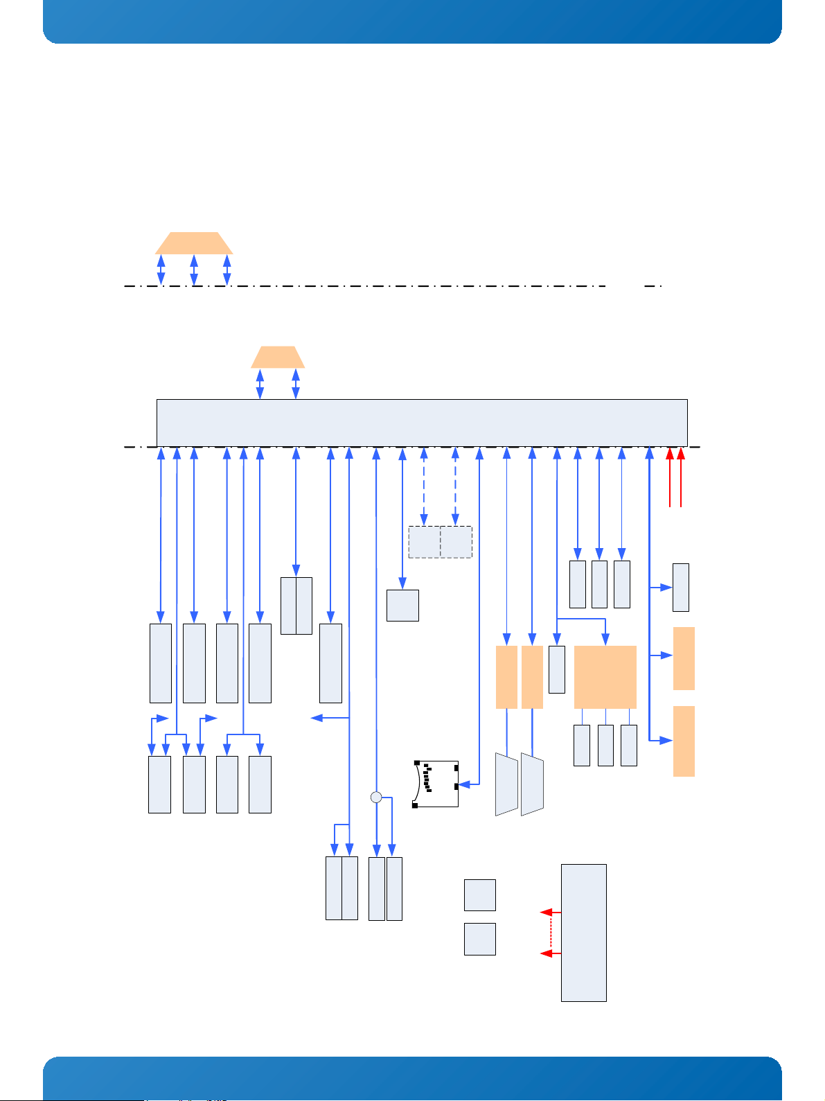
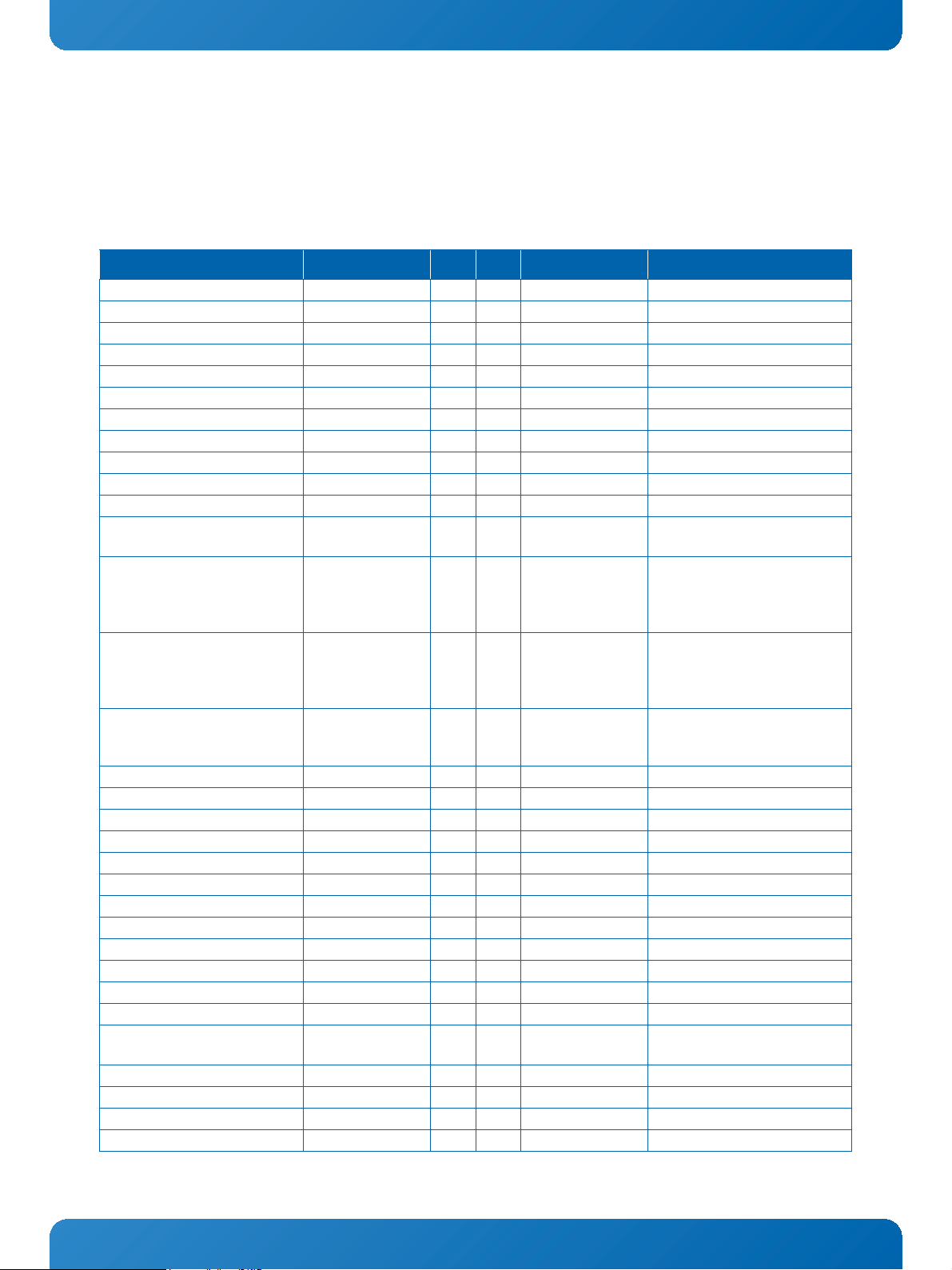
5 COME-QEC-1 Board Layout and Connectors
5.1 Board Layout
The following figure provides connector location, numerical designator, and connector pin numbering information. In addition, the locations of the DIP switch, the two push button switches, the battery holder and jumpers are illustrated.
Figure 2: Board Layout
5.2 Connectors
The following table provides an overview of the connectors available on the COME-QEC-1.
7
www.kontron.com
Page 8
Quick Start Guide
COME-QEC-1
Table 1: COME-QEC-1 Connector Overview
SIGNAL GROUP REFDES DESCRIPTION
ATX-Power J44 ATX Power Connector (24-pin)
J45 ATX 12V for Module (4-pin)
Battery Power BT1 Socket for backup power to the RTC on the COM Express module
COM Express J1 COM-Express Module Connector Rows A/B
J2 COM-Express Module Connector Rows C/D
CPLD-Prog J28 Reserved for factory use only
J43 Reserved for factory use only
DEBUG J27 Aurora Debugging Connector (contact Kontron Support for assistance before using)
J29 Sideband Signals for Aurora Debugging
Ethernet J5 Ethernet RJ45 cable connector for GBE0
J6 right Ethernet RJ45 cable connector for GBE1
J6 left Ethernet RJ45 cable connector for GBE2
FLASH J31 SPI-Flash Socket SO8 wide
I2C EXT EVAL J38 I2C header connector
IEEE-1588 J9 IEEE-1588 sideband signal connector
LOCAL BUS J22 Local Bus / GPIO connector
MICRO_SD J8 Micro SD-Card Slot
MISC J37 40 pin connector which carries miscellaneous signals that don't fit into other groups
PWR BUT EXT J41 alternative connection for external Power push button
RST BUT EXT J40 alternative connection for external reset push button
SATA J15 Standard Sata Cable connector
J21 Standard Sata Cable connector
JP5 RFU
SERIAL J7 lower D-SUB9 RS232/RS422 connector for UART0
J7 upper D-SUB9 RS232/RS422 connector for UART1
SLOT 1 J17 Slot 1 main connector
J23 Slot 1 sideband signal connector
SLOT 2 J18 Slot 2 main connector
J24 Slot 2 sideband signal connector
SLOT 3 J19 Slot 3 main connector
J25 Slot 3 sideband signal connector
SLOT 4 J20 Slot 4 main connector
J26 Slot 4 sideband signal connector
SM J16 Reserved for System Management Controller
J33 Reserved for System Management Controller
J34 Reserved for System Management Controller
SPI EXT J30 Reserved for manufacturing purposes
USB J14 USB connector for cable adapter
J3 USB Host connector Type A
J4 USB Device connector Type Mini-B
8
www.kontron.com
Page 9
Quick Start Guide
COME-QEC-1
5.2.1 COM Express® Module Connector Connectors J1 and J2
The pinout of the COM-Express® connectors on the COME-QEC-1, the COMe-bP5020 and the COMe-cP2020 boards are specifically
defined for usage with Freescale® QorIQ® CPUs. Steering member for this definition was the CPU manufacturer Freescale®. The
COM-Express® interface is based on two connectors with two rows (Rows A/B and Rows C/D) with 440 pins total (220 pins for
each of the two connectors). The pinouts for these two connectors are as follows
Table 2: Connector J1 Rows A and B Pinout
COMMENT SIGNAL PIN PIN SIGNAL COMMENT
GND A1 B1 GND
GBE0_MDI3- A2 B2 GBE0_ACT#
GBE0_MDI3+ A3 B3 1588_CLK_OUT accessible via J9
GBE0_LINK100# A4 B4 1588_PULSE_OUT1 accessible via J9
GBE0_LINK1000# A5 B5 1588_PULSE_OUT2 accessible via J9
GBE0_MDI2- A6 B6 1588_ALARM_OUT1 accessible via J9
GBE0_MDI2+ A7 B7 1588_ALARM_OUT2 accessible via J9
GBE0_LINK# A8 B8 1588_TRIG_IN1 accessible via J9
GBE0_MDI1- A9 B9 1588_TRIG_IN2 accessible via J9
GBE0_MDI1+ A10 B10 1588_CLK_IN accessible via J9
GND A11 B11 GND
GBE0_MDI0- A12 B12 PWRBTN# debounced signal of Power
switch SW2
GBE0_MDI0+ A13 B13 SMB_CK buffered version of this signal is
routed to Slot1..4 connectors;
these signals must be enabled
by DIP SW3-3
GBE0_CTREF A14 B14 SMB_DAT buffered version of this signal is
routed to Slot1..4 connectors;
these signals must be enabled
by DIP SW3-3
connected to carrier logic and
connector J37; pullup 8k2 to
V_3V3_STDBY on carrier
for use with COMe-bP5020 SATA0_TX+ A16 B16 SATA1_TX+ for use with COMe-bP5020
for use with COMe-bP5020 SATA0_TX- A17 B17 SATA1_TX- for use with COMe-bP5020
for use with COMe-bP5020 SATA0_RX+ A19 B19 SATA1_RX+ for use with COMe-bP5020
for use with COMe-bP5020 SATA0_RX- A20 B20 SATA1_RX- for use with COMe-bP5020
accessible via J37 BATLOW# A27 B27 WDT accessible via J37
reserved RFU A28..
reserved RFU A32 B32 RFU reserved
reserved RFU A33 B33 I2C_CK available on JP3
SUS_S3# A15 B15 SMB_ALERT# routed to carrier logic (actually
not used)
N/C A18 B18 N/C
GND A21 B21 GND
N/C A22 B22 N/C
N/C A23 B23 N/C
Reserved A24 B24 PWR_OK used to start onboard supply
N/C A25 B25 N/C
N/C A26 B26 N/C
B28..
RFU reserved
A30
B30
GND A31 B31 GND
N/C A34 B34 I2C_DAT available on JP2
9
www.kontron.com
Page 10

Quick Start Guide
COME-QEC-1
Table 2: Connector J1 Rows A and B Pinout (Continued)
COMMENT SIGNAL PIN PIN SIGNAL COMMENT
connected to carrier logic and
connector J37
accessible via J22 DMA2_DDONE0# A36 B36 DMA2_DREQ0# accessible via J22
accessible via J22 DMA2_DACK0# A37 B37 DMA1_DDONE0# accessible via J22
accessible via J22 LWE[1]# A38 B38 USB4_OC#
accessible via J14 USB2- A42 B42 USB3- accessible via J14
accessible via J14 USB2+ A43 B43 USB3+ accessible via J14
connected to power switch SW2 USB_2_3_OC A44 B44 USB_0_1_OC# connected to slot sideband con-
accessible via J23 USB0- A45 B45 USB1- accessible via J24
accessible via J23 USB0+ A46 B46 USB1+ accessible via J24
used to reset devices on slot 1 EXCD0_PERST# A48 B48 EXCD1_CPPE# used to detect an Add-In card in
used to detect an Add-In card in
slot1;
Attention: SERDES_CK_REF+/- is
shut-off on slot connector if no
card is detected
accessible via J22 LA16 / GPIO8 A50 B50 CB_RESET# used to reset devices on carrier
accessible via J18 SERDES_TX5+ A52 B52 SERDES_RX5+ accessible via J18
accessible via J18 SERDES_TX5- A53 B53 SERDES_RX5- accessible via J18
accessible via J18 SERDES_TX4+ A55 B55 SERDES_RX4+ accessible via J18
accessible via J18 SERDES_TX4- A56 B56 SERDES_RX4- accessible via J18
accessible via J17 SERDES_TX3+ A58 B58 SERDES_RX3+ accessible via J17
accessible via J17 SERDES_TX3- A59 B59 SERDES_RX3- accessible via J17
accessible via J17 SERDES_TX2+ A61 B61 SERDES_RX2+ accessible via J17
accessible via J17 SERDES_TX2 A62 B62 SERDES_RX2- accessible via J17
accessible via J17 SERDES_TX1+ A64 B64 SERDES_RX1+ accessible via J17
accessible via J17 SERDES_TX1- A65 B65 SERDES_RX1- accessible via J17
accessible via J17 SERDES_TX0+ A68 B68 SERDES_RX0+ accessible via J17
accessible via J17 SERDES_TX0- A69 B69 SERDES_RX0- accessible via J17
THRMTRIP A35 B35 THRM# connected to carrier logic and
connector J37
USB4- A39 B39 DMA1_DACK0# accessible via J22
USB4+ A40 B40 DMA1_DREQ0# accessible via J22
GND A41 B41 GND
nectors J23 and J24
VCC_RTC A47 B47 EXCD1_PERST# used to reset devices on slot 2
slot2;
Attention: SERDES_CK_REF+/- is
shut-off on slot connector if no
card is detected
EXCD0_CPPE# A49 B49 SYS_RESET# debounced signal of Reset
switch SW1
GND A51 B51 GND
SD_DATA0 A54 B54 SD_CMD
GND A57 B57 NC
GND A60 B60 GND
SD_DATA1 A63 B63 SD_CD#
GND A66 B66 WAKE0# connected to carrier logic (not
actually used); J17 and J18
SD_DATA2 A67 B67 WAKE1# connected to carrier logic (not
actually used); J19 and J20
GND A70 B70 GND
10
www.kontron.com
Page 11
Quick Start Guide
COME-QEC-1
Table 2: Connector J1 Rows A and B Pinout (Continued)
COMMENT SIGNAL PIN PIN SIGNAL COMMENT
N/C A71..
GND A80 B80 GND
N/C A81 B81 N/C
N/C A82 B82 N/C
Reserved A83 B83 N/C
Reserved A84 B84 VCC_5V_SBY
SD_DATA3 A85 B85 VCC_5V_SBY
accessible via J22 LA18 / GPIO10 A86 B86 VCC_5V_SBY
accessible via J22 LA17 / GPIO9 A87 B87 VCC_5V_SBY
connected to clock buffer SERDES_CK_REF+ A88 B88 BIOS_DIS1# can be set to logic ‘0’ with
connected to clock buffer SERDES_CK_REF- A89 B89 JTAG TCK manufacturing use
GND A90 B90 GND
3.3V supplied by module SPI_POWER A91 B91 JTAG TDI manufacturing use
SPI_MISO A92 B92 JTAG TMS manufacturing use
SD_CLK A93 B93 JTAG TDO manufacturing use
SPI_CLK A94 B94 N/C
SPI_MOSI A95 B95 Reserved
N/C A96 B96 Reserved
weak pullup to 3.3V T YPE10# A97 B97 SPI_CS#
SER0_TX A98 B98 EMI2_MDC Ethernet Management Clock for
SER0_RX A99 B99 EMI2_MDIO Ethernet Management In/Out
GND A100 B100 GND
SER1_TX A101 B101 Reserved
SER1_RX A102 B102 Reser ved
N/C A103 B103 Reserved
nominal 12V VCC_12V A104..
GND A110 B110 GND
A79
A109
B71..
N/C
B79
B104..
VCC_12V nominal 12V
B109
jumper J32
XAUI usage (1.2V signal level);
routed to slot sideband connectors J25 and J26
for XAUI usage (1.2V signal
level); routed to slot sideband
connectors J25 and J26
11
www.kontron.com
Page 12
Quick Start Guide
COME-QEC-1
Table 3: Connector J2 Rows C and D Pinout
COMMENT SIGNAL PIN PIN SIGNAL COMMENT
GND C1 D1 GND
for use with COMe-bP2020 GBE1_ACT# C2 D2 GBE2_ACT# for use with COMe-bP2020
for use with COMe-bP2020 GBE1_MDI3- C3 D3 GBE2_MDI3- for use with COMe-bP2020
for use with COMe-bP2020 GBE1_MDI3+ C4 D4 GBE2_MDI3+ for use with COMe-bP2020
for use with COMe-bP2020 GBE1_LINK100# C5 D5 GBE2_LINK100# for use with COMe-bP2020
for use with COMe-bP2020 GBE1_MDI2- C6 D6 GBE2_MDI2- for use with COMe-bP2020
for use with COMe-bP2020 GBE1_MDI2+ C7 D7 GBE2_MDI2+ for use with COMe-bP2020
for use with COMe-bP2020 GBE1_LINK1000# C8 D8 GBE2_LINK1000# for use with COMe-bP2020
for use with COMe-bP2020 GBE1_MDI1- C9 D9 GBE2_MDI1- for use with COMe-bP2020
for use with COMe-bP2020 GBE1_MDI1+ C10 D10 GBE2_MDI1+ for use with COMe-bP2020
GND C11 D11 GND
for use with COMe-bP2020 GBE1_MDI0- C12 D12 GBE2_MDI0- for use with COMe-bP2020
for use with COMe-bP2020 GBE1_MDI0+ C13 D13 GBE2_MDI0+ for use with COMe-bP2020
for use with COMe-bP2020 GBE1_LINK# C14 D14 GBE2_LINK# for use with COMe-bP2020
NC C15 D15 NC
NC C16 D16 NC
accessible via J22 LOE# C17 D17 LCS0# accessible via J22
accessible via J22 LWE[0]# C18 D18 LCS1# accessible via J22
accessible via J18 SERDES_RX6+ C19 D19 SERDES_TX6+ accessible via J18
accessible via J18 SERDES_RX6- C20 D20 SERDES_TX6- accessible via J18
GND C21 D21 GND
accessible via J18 SERDES_RX7+ C22 D22 SERDES_TX7+ accessible via J18
accessible via J18 SERDES_RX7- C23 D23 SERDES_TX7- accessible via J18
N/C C24 D24 LA31 accessible via J22
N/C C25 D25 LA30 accessible via J22
N/C C26 D26 N/C
accessible via J22 LAD0 C27 D27 N/C
accessible via J22 LAD1 C28 D28 GND
N/C C29 D29 N/C
N/C C30 D30 N/C
GND C31 D31 GND
accessible via J22 LAD2 C32 D32 N/C
accessible via J22 LAD3 C33 D33 N/C
accessible via J22 LAD4 C34 D34 N/C
accessible via J22 LAD5 C35 D35 LALE accessible via J22
accessible via J22 LAD6 C36 D36 N/C
accessible via J22 LAD7 C37 D37 N/C
accessible via J22 LAD8 / GPIO0 C38 D38 GND
accessible via J22 LAD9 / GPIO1 C39 D39 SER0_CTS#
accessible via J22 LAD10 / GPIO2 C40 D40 SER0_RTS#
GND C41 D41 GND
accessible via J22 LAD11 / GPIO3 C42 D42 SER1_CTS#
accessible via J22 LAD12 / GPIO4 C43 D43 SER1_RTS#
accessible via J22 LAD13 / GPIO5 C44 D44 LBCTL accessible via J22
accessible via J22 LAD14 / GPIO6 C45 D45 LGTA# accessible via J22
accessible via J22 LAD15 / GPIO7 C46 D46 IRQ3# / GPIO connected to carrier logic (not
actually used) and J25
12
www.kontron.com
Page 13

Quick Start Guide
COME-QEC-1
Table 3: Connector J2 Rows C and D Pinout (Continued)
COMMENT SIGNAL PIN PIN SIGNAL COMMENT
Ethernet Management Clock for
SGMII PHY; routed to slot sideband connector J23
Ethernet Management In/Out
for SGMII PHY; routed to slot
sideband connector J23
accessible via J37 IRQ1# / GPIO C49 D49 LA28 accessible via J22
accessible via J37 IRQ2# / GPIO C50 D50 IRQ_OUT# connected to carrier logic and
accessible via J27 SERDES_RX8+ C52 D52 SERDES_TX8+ accessible via J27
accessible via J27 SERDES_RX8- C53 D53 SERDES_TX8- accessible via J27
accessible via J27 SERDES_RX9+ C55 D55 SERDES_TX9+ accessible via J27
accessible via J27 SERDES_RX9- C56 D56 SERDES_TX9- accessible via J27
accessible via J19 SERDES_RX10+ C58 D58 SERDES_TX10+ accessible via J19
accessible via J19 SERDES_RX10- C59 D59 SERDES_TX10- accessible via J19
accessible via J19 SERDES_RX11+ C61 D61 SERDES_TX11+ accessible via J19
accessible via J19 SERDES_RX11- C62 D62 SERDES_TX11- accessible via J19
accessible via J22 LA25 C63 D63 LA27 accessible via J22
accessible via J22 LA24 C64 D64 LA26 accessible via J22
accessible via J19 SERDES_RX12+ C65 D65 SERDES_TX12+ accessible via J19
accessible via J19 SERDES_RX12- C66 D66 SERDES_TX12- accessible via J19
accessible via J22 LA23 C67 D67 GND
accessible via J19 SERDES_RX13+ C68 D68 SERDES_TX13+ accessible via J19
accessible via J19 SERDES_RX13- C69 D69 SERDES_TX13- accessible via J19
accessible via J20 SERDES_RX14+ C71 D71 SERDES_TX14+ accessible via J20
accessible via J20 SERDES_RX14- C72 D72 SERDES_TX14- accessible via J20
accessible via J20 SERDES_RX15+ C74 D74 SERDES_TX15+ accessible via J20
accessible via J20 SERDES_RX15- C75 D75 SERDES_TX15- accessible via J20
accessible via J22 LA22 C77 D77 IRQ5# / GPIO connected to carrier logic (not
accessible via J20 SERDES_RX16+ C78 D78 SERDES_TX16+ accessible via J20
accessible via J20 SERDES_RX16- C79 D79 SERDES_TX16- accessible via J20
accessible via J20 SERDES_RX17+ C81 D81 SERDES_TX17+ accessible via J20
accessible via J20 SERDES_RX17- C82 D82 SERDES_TX17- accessible via J20
accessible via J22 LA21 C83 D83 TYPE3# connected to carrier logic (with
EMI1_MDC C47 D47 IRQ4# / GPIO connected to carrier logic (not
actually used) and J26
EMI1_MDIO C48 D48 LA29 accessible via J22
connector J37
GND C51 D51 GND
TYPE0# C54 D54 Reserved
TYPE1# C57 D57 T YPE2# connected to carrier logic (with
weak pullup)
GND C60 D60 GND
GND C70 D70 GND
GND C73 D73 GND
GND C76 D76 GND
actually used) and J37
GND C80 D80 GND
weak pullup)
GND C84 D84 GND
N/C C85 D85 N/C
N/C C86 D86 N/C
13
www.kontron.com
Page 14

Quick Start Guide
Table 3: Connector J2 Rows C and D Pinout (Continued)
COMMENT SIGNAL PIN PIN SIGNAL COMMENT
GND C87 D87 GND
N/C C88 D88 N/C
N/C C89 D89 N/C
GND C90 D90 GND
N/C C91 D91 N/C
N/C C92 D92 N/C
GND C93 D93 GND
N/C C93 D93 N/C
N/C C94 D94 N/C
GND C96 D96 GND
accessible via J22 LA20 C97 D97 LA19 / GPIO11 accessible via J22
N/C C98 D98 N/C
N/C C99 D99 N/C
GND C100 D100 GND
N/C C101 D101 N/C
N/C C102 D102 N/C
GND C103 D103 GND
nominal 12V VCC_12V C104..
GND C110 D110 GND
C109
D104..
VCC_12V nominal 12V
D109
COME-QEC-1
14
www.kontron.com
Page 15

Quick Start Guide
COME-QEC-1
5.2.2 USB Connectors J3/J4/J14
The COME-QEC-1 provides connectivity for up to five USB-Host ports or four USB-Host ports and one USB-Device port. Connectors J3 and J4 share a common USB port which must be configured either as a host or a device port.
Directly usable:
» J3: USB-Device-Port (USB type B connector)
» J4: USB-Host-Port (USB type A connector)
» J14: Header for connecting a standard USB cable assembly (included with the EVAL-Kit) providing two USB-Host-Ports (USB
type A connectors).
Furthermore, there are two USB host ports routed to the Slot 1 sideband connector (J23) and the Slot 2 sideband connector
(J24). These two ports can be evaluated either by using the connectors on the ADAP-EVAL-QORIQ-SRIO Adapter Card or can be
used by Add-In cards which are specially designed for customer purposes.
Please refer also to the pinout table of connectors J23 and J24 and Chapter 9.3 Adapter Card ADAP-EVAL-QORIQ-SRIO.
5.2.3 Ethernet Connectors J5/J6L/J6R
The COME-QEC-1 provides RJ45 connectors, J5 and J6 Right and Left, for up to three Gigabit Ethernet copper interfaces
(ETH0..ETH2 on connectors J5 and J6). If the carrier is equipped with the COMe-bP5020, only ETH0 (J5) is supported. In configurations with the COMe-cP2020 all three RJ45 connectors are usable for GbE interfacing.
5.2.4 Serial Interface Connectors J7 Upper and Lower
The COME-QEC-1 provides two D-SUB9 connectors for serial UART interfacing. The connector pinout is as follows (depending on
the module and carrier configuration). The configuration of these interfaces for RS232 or RS422 operation is done using DIP
switch SW3 switches 1 and 2.
Table 4: D-SUB9 Serial UART Connectors J7 (Upper and Lower) Pinout
PIN RS232 SIGNALS RS422 SIGNALS
1 High-Z RS422 RX+
2 RS232 RxD High-Z
3 RS232 TxD RS422 TX+
4NC NC
5GND GND
6 High-Z RS422 RX-
7 RS232 RTS# High-Z
8 RS232 CTS# RS422 TX-
9NC NC
For RS422 operation, jumpers J10 (COM0 TX), J11 (COM1 TX), J12 (COM1 RX) and J13 (COM0 RX) are provided for signal line
termination as required.
5.2.5 microSD/SDHC Card Connector J8
The COME-QEC-1 evaluation carrier is equipped with a microSD/SDHC card socket J8 which provides the possibility to extend
the mass storage capability of the COMe-bP5020 or the COMe-cP2020 with an external SD/SDHC card of up to 32GB. This device
can be used as a boot device or for data storage.
Note: This socket is multiplexed with the on-board SD/SDHC card socket of the COMe-bP5020 or COMe-cP2020. Please ensure
that the configuration of the COM Express® module is done correctly for the usage of this socket.
15
www.kontron.com
Page 16

Quick Start Guide
COME-QEC-1
5.2.6 IEEE-1588 Sideband Signal Connector J9
The COME-QEC-1 provides a pinrow header for gaining access to the QorIQ™ IEEE-1588 sideband signals. For more information
about the functionality of these signals please refer to the respective processor’s reference manuals.
Table 5: IEEE-1588 Sideband Signal Connector J9 Pinout
SIGNAL PIN PIN SIGNAL
V_3V3 1 2 GND
1588_PULSE_OUT1 3 4 1588_CLK_OUT
1588_PULSE_OUT2 5 6 1588_ALARM_OUT1
NC 7 8 1588_ALARM_OUT2
1588_TRIG_IN1 9 10 1588_CLK_IN
1588_TRIG_IN2 11 12 GND
5.2.7 SATA Connectors J15/J21
The COME-QEC-1 provides two standard SATA cable connectors (J15 and J21) which can be used for the evaluation of the COMebP5020 SATA ports. These connectors can be used to connect to hard disk drives, SSD drives, etc. Power for the connected device must be provided externally, for instance by the ATX power supply.
Note: For the usage of the COME-QEC-1 in conjunction with the COMe-cP2020 these connectors are not operable.
16
www.kontron.com
Page 17

Quick Start Guide
COME-QEC-1
5.2.8 SLOT 1 Connector J17
Slot 1 and its dedicated sideband signal connector J23 provide the possibility to verify the PCIe and sRIO capability of the
mounted COM Express® module. The main connector J17 provides the x4 interface connectivity whereas the sideband connector adds several sideband signals which are necessary for operation of the S0012 SRIO-Adapter Card or to assist in designing
special custom adapter cards.
Table 6: SLOT 1 Connector J17 Pinout
COMMENT
12V power supply V_12V+ 1 1 PRSNT1# Grounded
12V power supply V_12V+ 2 2 V_12V+ 12V power supply
12V power supply V_12V+ 3 3 V_12V+ 12V power supply
Ground GND 4 4 GND Ground
SMBus clock from
COME module
(refer to Table 20)
SMBus data from/
to COME module
(refer to Table 20)
Ground GND 7 7 NC Not connected
3.3V power supply V_3V3 8 8 NC Not connected
Not connected NC 9 9 V_3V3 3.3V power supply
3.3V power supply V_3V3 10 10 V_3V3 3.3V power supply
Wake0# signal to
COME module
Not connected NC 12 12 GND Ground
Ground GND 13 13 CLK_PCIE_SLOT1+ buf fered signal
SerDes transmitter differential
pair, Lane 0
Ground GND 16 16 SLOT1_SD_RX[0]+ SERDES_RX0+ SerDes receiver
EXCD0_CPPE# signal to COME module, PRSNT# card
detect signal to
carrier glue logic,
8k2 PU on carrier
to V_3V3_STDBY
Ground GND 18 18 GND Ground
SerDes transmitter differential
pair, Lane 1
COM EXPRESS
CONNECTION
buffered signal
of SMB_CK
buffered signal
of SMB_DAT
WAKE[0]# WAKE[0]# 11 11 RESET_PCIE_SLOT1# PCIe Reset from
SERDES_TX0+ SLOT1_SD_TX[0]+ 14 14 CLK_PCIE_SLOT1- buf fered signal
SERDES_TX0- SLOT1_SD_TX[0]- 15 15 GND Ground
EXCD0_CPPE# EXCD0_CPPE# 17 17 SLOT1_SD_RX[0]- SERDES_RX0-
SERDES_TX1+ SLOT1_SD_TX[1]+ 19 19 NC Not connected
SIGNAL
I2C_SMB_SCL 5 5 NC Not connected
I2C_SMB_SDA 6 6 NC Not connected
PIN SIDE
B A
SIGNAL
COM EXPRESS
CONNECTION
of SERDES_
CK_REF+
of SERDES_
CK_REF-
COMMENT
Carrier glue logic,
low active
100MHz PCIe reference clock, differential pair
differential pair,
Lane 0
17
www.kontron.com
Page 18

Table 6: SLOT 1 Connector J17 Pinout (Continued)
Quick Start Guide
COME-QEC-1
COMMENT
Ground GND 21 21 SLOT1_SD_RX[1]+ SERDES_RX1+ SerDes receiver
Ground GND 22 22 SLOT1_SD_RX[1]- SERDES_RX1-
SerDes transmitter differential
pair, Lane 2
Ground GND 25 25 SLOT1_SD_RX[2]+ SERDES_RX2+ SerDes receiver
Ground GND 26 26 SLOT1_SD_RX[2]- SERDES_RX2-
SerDes transmitter differential
pair, Lane 3
Ground GND 29 29 SLOT1_SD_RX[3]+ SERDES_RX3+ SerDes receiver
Not connected NC 30 30 SLOT1_SD_RX[3]- SERDES_RX3-
EXCD0_CPPE# signal to COME module, PRSNT# card
detect signal to
carrier glue logic,
8k2 PU on carrier
to V_3V3_STDBY
Ground GND 32 32 NC Not connected
COM EXPRESS
CONNECTION
SERDES_TX1- SLOT1_SD_TX[1]- 20 20 GND Ground
SERDES_TX2+ SLOT1_SD_TX[2]+ 23 23 GND Ground
SERDES_TX2- SLOT1_SD_TX[2]- 24 24 GND Ground
SERDES_TX3+ SLOT1_SD_TX[3]+ 27 27 GND Ground
SERDES_TX3- SLOT1_SD_TX[3]- 28 28 GND Ground
EXCD0_CPPE# EXCD0_CPPE# 31 31 GND Ground
SIGNAL
PIN SIDE
B A
SIGNAL
COM EXPRESS
CONNECTION
COMMENT
differential pair,
Lane 1
differential pair,
Lane 2
differential pair,
Lane 3
18
www.kontron.com
Page 19

Quick Start Guide
COME-QEC-1
5.2.9 SLOT 2 Connector J18
Slot 2 and its dedicated sideband signal connector J24 provide the possibility to verify the PCIe and sRIO capability of the
mounted COM Express® module. The main connector J18 provides the x4 interface connectivity whereas the sideband connector adds several sideband signals which are necessary for operation of the S0012 SRIO-Adapter Card or to assist in designing
special custom adapter cards.
Table 7: SLOT 2 Connector J18 Pinout
COMMENT
12V power supply V_12V+ 1 1 PRSNT1# Grounded
12V power supply V_12V+ 2 2 V_12V+ 12V power supply
12V power supply V_12V+ 3 3 V_12V+ 12V power supply
Ground GND 4 4 GND Ground
SMBus clock from
COME module
(refer to Table 20)
SMBus data from/
to COME module
(refer to Table 20)
Ground GND 7 7 NC Not connected
3.3V power supply V_3V3 8 8 NC Not connected
Not connected NC 9 9 V_3V3 3.3V power supply
3.3V power supply V_3V3 10 10 V_3V3 3.3V power supply
Wake0# signal to
COME module
Not connected NC 12 12 GND Ground
Ground GND 13 13 CLK_PCIE_SLOT2+ buf fered signal
SerDes transmitter differential
pair, Lane 0
Ground GND 16 16 SLOT2_SD_RX[0]+ SERDES_RX4+ SerDes receiver
EXCD0_CPPE# signal to COME module, PRSNT# card
detect signal to
carrier glue logic,
8k2 PU on carrier
to V_3V3_STDBY
COM EXPRESS
CONNECTION
buffered signal
of SMB_CK
buffered signal
of SMB_DAT
WAKE0# WAKE[0]# 11 11 RESET_PCIE_SLOT2# PCIe Reset from
SERDES_TX4+ SLOT2_SD_TX[0]+ 14 14 CLK_PCIE_SLOT2- buf fered signal
SERDES_TX4- SLOT2_SD_TX[0]- 15 15 GND Ground
EXCD1_CPPE# EXCD1_CPPE# 17 17 SLOT2_SD_RX[0]- SERDES_RX4-
SIGNAL
I2C_SMB_SCL 5 5 NC Not connected
I2C_SMB_SDA 6 6 NC Not connected
PIN SIDE
B A
SIGNAL
COM EXPRESS
CONNECTION
of
SERDES_CK_RE
F+
of
SERDES_CK_RE
F-
COMMENT
Carrier glue logic,
low active
100MHz PCIe reference clock, differential pair
differential pair,
Lane 0
19
www.kontron.com
Page 20

Table 7: SLOT 2 Connector J18 Pinout (Continued)
Quick Start Guide
COME-QEC-1
COMMENT
Ground GND 18 18 GND Ground
SerDes transmitter differential
pair, Lane 1
Ground GND 21 21 SLOT2_SD_RX[1]+ SERDES_RX5+ SerDes receiver
Ground GND 22 22 SLOT2_SD_RX[1]- SERDES_RX5-
SerDes transmitter differential
pair, Lane 2
Ground GND 25 25 SLOT2_SD_RX[2]+ SERDES_RX6+ SerDes receiver
Ground GND 26 26 SLOT2_SD_RX[2]- SERDES_RX6-
SerDes transmitter differential
pair, Lane 3
Ground GND 29 29 SLOT2_SD_RX[3]+ SERDES_RX7+ SerDes receiver
Not connected NC 30 30 SLOT2_SD_RX[3]- SERDES_RX7-
EXCD0_CPPE# signal to COME module, PRSNT# card
detect signal to
carrier glue logic,
8k2 PU on carrier
to V_3V3_STDBY
Ground GND 32 32 NC Not connected
COM EXPRESS
CONNECTION
SERDES_TX5+ SLOT2_SD_TX[1]+ 19 19 NC Not connected
SERDES_TX5- SLOT2_SD_TX[1]- 20 20 GND Ground
SERDES_TX6+ SLOT2_SD_TX[2]+ 23 23 GND Ground
SERDES_TX6- SLOT2_SD_TX[2]- 24 24 GND Ground
SERDES_TX7+ SLOT2_SD_TX[3]+ 27 27 GND Ground
SERDES_TX7- SLOT2_SD_TX[3]- 28 28 GND Ground
EXCD1_CPPE# EXCD1_CPPE# 31 31 GND Ground
SIGNAL
PIN SIDE
B A
SIGNAL
COM EXPRESS
CONNECTION
COMMENT
differential pair,
Lane 1
differential pair,
Lane 2
differential pair,
Lane 3
20
www.kontron.com
Page 21

Quick Start Guide
COME-QEC-1
5.2.10 SLOT 3 Connector J19
Slot 3 and its dedicated sideband signal connector J25 provide the possibility to verify the SGMII and XAUI capability of the
mounted COM Express® module. The main connector J19 provides up to four GigEthernet SGMII interfaces or one XAUI interface
whereas the sideband connector adds several sideband signals which are necessary for operation of the S0010 SGMII-Adapter
Card or the S0011 XAUI-Adapter Card or to assist in designing special custom adapter cards.
Table 8: SLOT 3 Connector J19 Pinout
COMMENT
12V power supply V_12V+ 1 1 NC Not connected
12V power supply V_12V+ 2 2 V_12V+ 12V power supply
12V power supply V_12V+ 3 3 V_12V+ 12V power supply
Ground GND 4 4 GND Ground
SMBus clock from
COME module
(refer to Table 20)
SMBus data from/
to COME module
(refer to Table 20)
Ground GND 7 7 NC Not connected
3.3V power supply V_3V3 8 8 NC Not connected
Not connected NC 9 9 V_3V3 3.3V power supply
3.3V power supply V_3V3 10 10 V_3V3 3.3V power supply
Wake1# signal to
COME module
Not connected NC 12 12 GND Ground
Ground GND 13 13 NC Not connected
SerDes transmitter differential
pair, Lane 0
Ground GND 16 16 SLOT3_SD_RX[0]+ SERDES_RX10+ SerDes receiver
Not connected NC 17 17 SLOT3_SD_RX[0]- SERDES_RX10-
Ground GND 18 18 GND Ground
SerDes transmitter differential
pair, Lane 1
Ground GND 21 21 SLOT3_SD_RX[1]+ SERDES_RX11+ SerDes receiver
Ground GND 22 22 SLOT3_SD_RX[1]- SERDES_RX11-
COM EXPRESS
CONNECTION
buffered signal
of SMB_CK
buffered signal
of SMB_DAT
WAKE1# WAKE[1]# 11 11 RESET_PCIE_SLOT3# PCIe Reset from
SERDES_TX10+ SLOT3_SD_TX[0]+ 14 14 NC Not connected
SERDES_TX10- SLOT3_SD_TX[0]- 15 15 GND Ground
SERDES_TX11+ SLOT3_SD_TX[1]+ 19 19 NC Not connected
SERDES_TX11- SLOT3_SD_TX[1]- 20 20 GND Ground
SIGNAL
I2C_SMB_SCL 5 5 NC Not connected
I2C_SMB_SDA 6 6 NC Not connected
PIN SIDE
B A
SIGNAL
COM EXPRESS
CONNECTION
COMMENT
Carrier glue logic,
low active
differential pair,
Lane 0
differential pair,
Lane 1
21
www.kontron.com
Page 22

Table 8: SLOT 3 Connector J19 Pinout (Continued)
Quick Start Guide
COME-QEC-1
COMMENT
SerDes transmitter differential
pair, Lane 2
Ground GND 25 25 SLOT3_SD_RX[2]+ SERDES_RX12+ SerDes receiver
Ground GND 26 26 SLOT3_SD_RX[2]- SERDES_RX12-
SerDes transmitter differential
pair, Lane 3
Ground GND 29 29 SLOT3_SD_RX[3]+ SERDES_RX13+ SerDes receiver
Not connected NC 30 30 SLOT3_SD_RX[3]- SERDES_RX13-
Not connected NC 31 31 GND Ground
Ground GND 32 32 NC Not connected
COM EXPRESS
CONNECTION
SERDES_TX12+ SLOT3_SD_TX[2]+ 23 23 GND Ground
SERDES_TX12- SLOT3_SD_TX[2]- 24 24 GND Ground
SERDES_TX13+ SLOT3_SD_TX[3]+ 27 27 GND Ground
SERDES_TX13- SLOT3_SD_TX[3]- 28 28 GND Ground
SIGNAL
PIN SIDE
B A
SIGNAL
COM EXPRESS
CONNECTION
COMMENT
differential pair,
Lane 2
differential pair,
Lane 3
22
www.kontron.com
Page 23

Quick Start Guide
COME-QEC-1
5.2.11 SLOT 4 Connector J20
Slot 4 and its dedicated sideband signal connector J26 provide the possibility to verify the SGMII and XAUI capability of the
mounted COM Express® module. The main connector J20 provides up to four GigEthernet SGMII interfaces or one XAUI interface
whereas the sideband connector adds several sideband signals which are necessary for operation of the S0011 XAUI-Adapter
Card or to assist in designing special custom adapter cards.
Table 9: SLOT 4 Connector J20 Pinout
COMMENT
12V power supply V_12V+ 1 1 NC Not connected
12V power supply V_12V+ 2 2 V_12V+ 12V power supply
12V power supply V_12V+ 3 3 V_12V+ 12V power supply
Ground GND 4 4 GND Ground
SMBus clock from
COME module
(refer to Table 20)
SMBus data from/
to COME module
(refer to Table 20)
Ground GND 7 7 NC Not connected
3.3V power supply V_3V3 8 8 NC Not connected
Not connected NC 9 9 V_3V3 3.3V power supply
3.3V power supply V_3V3 10 10 V_3V3 3.3V power supply
Wake1# signal to
COME module
Not connected NC 12 12 GND Ground
Ground GND 13 13 NC Not connected
SerDes transmitter differential
pair, Lane 0
Ground GND 16 16 SLOT4_SD_RX[0]+ SERDES_RX14+ SerDes receiver
Not connected NC 17 17 SLOT4_SD_RX[0]- SERDES_RX14-
Ground GND 18 18 GND Ground
SerDes transmitter differential
pair, Lane 1
Ground GND 21 21 SLOT4_SD_RX[1]+ SERDES_RX15+ SerDes receiver
Ground GND 22 22 SLOT4_SD_RX[1]- SERDES_RX15-
COM EXPRESS
CONNECTION
buffered signal
of SMB_CK
buffered signal
of SMB_DAT
WAKE1# WAKE[1]# 11 11 RESET_PCIE_SLOT4# PCIe Reset from
SERDES_TX14+ SLOT4_SD_TX[0]+ 14 14 NC Not connected
SERDES_TX14- SLOT4_SD_TX[0]- 15 15 GND Ground
SERDES_TX15+ SLOT4_SD_TX[1]+ 19 19 NC Not connected
SERDES_TX15- SLOT4_SD_TX[1]- 20 20 GND Ground
SIGNAL
I2C_SMB_SCL 5 5 NC Not connected
I2C_SMB_SDA 6 6 NC Not connected
PIN SIDE
B A
SIGNAL
COM EXPRESS
CONNECTION
COMMENT
Carrier glue logic,
low active
differential pair,
Lane 0
differential pair,
Lane 1
23
www.kontron.com
Page 24

Table 9: SLOT 4 Connector J20 Pinout (Continued)
Quick Start Guide
COME-QEC-1
COMMENT
SerDes transmitter differential
pair, Lane 2
Ground GND 25 25 SLOT4_SD_RX[2]+ SERDES_RX16+ SerDes receiver
Ground GND 26 26 SLOT4_SD_RX[2]- SERDES_RX16-
SerDes transmitter differential
pair, Lane 3
Ground GND 29 29 SLOT4_SD_RX[3]+ SERDES_RX17+ SerDes receiver
Not connected NC 30 30 SLOT4_SD_RX[3]- SERDES_RX17-
Not connected NC 31 31 GND Ground
Ground GND 32 32 NC Not connected
COM EXPRESS
CONNECTION
SERDES_TX16+ SLOT4_SD_TX[2]+ 23 23 GND Ground
SERDES_TX16- SLOT4_SD_TX[2]- 24 24 GND Ground
SERDES_TX17+ SLOT4_SD_TX[3]+ 27 27 GND Ground
SERDES_TX17- SLOT4_SD_TX[3]- 28 28 GND Ground
SIGNAL
PIN SIDE
B A
SIGNAL
COM EXPRESS
CONNECTION
COMMENT
differential pair,
Lane 2
differential pair,
Lane 3
24
www.kontron.com
Page 25

Quick Start Guide
COME-QEC-1
5.2.12 Local Bus / GPIO connector J22
The COM Express® modules COMe-cP2020 and COMe-bP5020 provide the possibility to connect parallel bus devices (SRAM style)
to their Local Bus. If such interfacing is required please contact Kontron Support for further assistance.
In addition to connecting devices to the Local Bus, the COMe-bP5020 provides twelve GPIOs which are multiplexed within the
Local Bus area. To use these IOs appropriate settings must be selected using the U-Boot SCONF command.
Table 10: Local Bus/GPIO Connector Pinout J22
SIGNAL PIN PIN SIGNAL
V_3V3 1 2 GND
LB_CS[0]# 3 4 NC
LB_OE# 5 6 LB_CS[1]#
LB_A[31] 7 8 LB_WE[0]#
LB_AD[0] 9 10 LB_A[30]
DMA2_DONE0# 11 12 LB_AD[1]
LB_WE[1]# 13 14 DMA2_DACK0#
DMA2_DREQ0# 15 16 DMA1_DONE0#
DMA1_DACK0# 17 18 DMA1_DREQ0#
LB_AD[3] 19 20 LB_AD[2]
LB_ALE 21 22 LB_AD[4]
LB_AD[6] 23 24 LB_AD[5]
LB_AD[8] / GPIO[0] 25 26 LB_AD[7]
LB_AD[10] / GPIO[2] 27 28 LB_AD[9] / GPIO[1]
LB_AD[11] / GPIO[3] 29 30 LB_CTL
LB_AD[12] / GPIO[4] 31 32 LB_GTA
LB_AD[14] / GPIO[6] 33 34 LB_AD[13] / GPIO[5]
LB_A[29] 35 36 LB_AD[15] / GPIO[7]
LB_A[16] / GPIO[8] 37 38 LB_A[28]
LB_A[27] 39 40 LB_A[25]
LB_A[24] 41 42 LB_A[26]
LB_A[22] 43 44 LB_A[23]
LB_A[18] / GPIO[10] 45 46 LB_A[21]
LB_A[20] 47 48 LB_A[17] / GPIO[9]
GND 49 50 LB_A[19] / GPIO[11]
25
www.kontron.com
Page 26

5.2.13 SLOT 1 Sideband Connector J23
Table 11: SLOT 1 Sideband Connector J23 Pinout
Quick Start Guide
COME-QEC-1
COMMENT
Not connected NC 1 1 NC Not connected
Not connected NC 2 2 NC Not connected
Not connected NC 3 3 NC Not connected
Ground GND 4 4 GND Ground
Not connected NC 5 5 SLOT1_I2C_ADDR1 Slot1 I2C address
Not connected NC 6 6 SLOT1_I2C_ADDR2 Slot1 I2C address
Ground GND 7 7 SLOT1_DEV_ADDR0 Slot1 DEV address
Not connected NC 8 8 SLOT1_DEV_ADDR1 Slot1 DEV address
Slot1 I2C address
coding: 1k to GND
Not connected NC 10 10 NC Not connected
USB overcurrent
status signal to
COME module
GPIO from/to carrier glue logic
Ground GND 13 13 NC Not connected
USB differential
pair from/to COME
module
Ground GND 16 16 NC Not connected
EXCD0_CPPE# signal to COME module, PRSNT# card
detect signal to
carrier glue logic,
8k2 PU on carrier
to V_3V3_STDBY
Ground GND 18 18 GND Ground
COM EXPRESS
CONNECTION
USB_0_1_OC# USB_P0_1_OC# 11 11 WLAN_DISABLE# WLAN disable out-
USB0+ USB_P[0]+ 14 14 NC Not connected
USB0- USB_P[0]- 15 15 GND Ground
EXCD0_CPPE# EXCD0_CPPE# 17 17 NC Not connected
SIGNAL
SLOT1_I2C_ADDR0 9 9 NC Not connected
SLOT1_GPIO 12 12 GND Ground
PIN ROW
B A
SIGNAL
COM EXPRESS
CONNECTION
COMMENT
coding: 1k to GND
coding: NC
coding: NC
coding: NC
put from glue logic
26
www.kontron.com
Page 27

5.2.14 SLOT 2 Sideband Connector J24
Table 12: SLOT 2 Sideband Connector J24 Pinout
Quick Start Guide
COME-QEC-1
COMMENT
Not connected NC 1 1 NC Not connected
Not connected NC 2 2 NC Not connected
Not connected NC 3 3 NC Not connected
Ground GND 4 4 GND Ground
Not connected NC 5 5 SLOT2_I2C_ADDR1 Slot2 I2C address
Not connected NC 6 6 SLOT2_I2C_ADDR2 Slot2 I2C address
Ground GND 7 7 SLOT2_DEV_ADDR0 Slot2 DEV address
Not connected NC 8 8 SLOT2_DEV_ADDR1 Slot2 DEV address
Slot2 I2C address
coding: NC
Not connected NC 10 10 NC Not connected
USB overcurrent
status signal to
COME module
GPIO from/to carrier glue logic
Ground GND 13 13 NC Not connected
USB differential
pair from/to COME
module
Ground GND 16 16 NC Not connected
EXCD0_CPPE# signal to COME module, PRSNT# card
detect signal to
carrier glue logic,
8k2 PU on carrier
to V_3V3_STDBY
Ground GND 18 18 GND Ground
COM EXPRESS
CONNECTION
USB_0_1_OC# USB_P0_1_OC# 11 11 WLAN_DISABLE# WLAN disable out-
USB1+ USB_P[1]+ 14 14 NC Not connected
USB1- USB_P[1]- 15 15 GND Ground
EXCD1_CPPE# EXCD1_CPPE# 17 17 NC Not connected
SIGNAL
SLOT2_I2C_ADDR0 9 9 NC Not connected
SLOT2_GPIO 12 12 GND Ground
PIN ROW
B A
SIGNAL
COM EXPRESS
CONNECTION
COMMENT
coding: NC
coding: 1k PD to
GND
coding: 1k PD to
GND
coding: NC
put from glue logic
27
www.kontron.com
Page 28

5.2.15 SLOT 3 Sideband Connector J25
Table 13: SLOT 3 Sideband Connector J25 Pinout
Quick Start Guide
COME-QEC-1
COMMENT
Not connected NC 1 1 NC Not connected
Not connected NC 2 2 NC Not connected
Not connected NC 3 3 NC Not connected
Ground GND 4 4 GND Ground
Management
Interface for 10G
PHY (1.2V signal
level)
Ground GND 7 7 SLOT3_PHY_ADDR3 PHY address 3 sig-
Not connected NC 8 8 SLOT3_PHY_ADDR4 PHY address 4 sig-
PHY address 0 signal: NC
Not connected NC 10 10 NC Not connected
Interrupt to COME
module
GPIO from/to
carrier glue logic
Ground GND 13 13 EMI1_MDC_1G EMI1_MDC Management
Not connected NC 14 14 EMI1_MDIO_1G EMI1_MDIO
Not connected NC 15 15 GND
Ground GND 16 16 NC Not connected
Not connected NC 17 17 NC Not connected
Ground GND 18 18 GND Ground
COM EXPRESS
CONNECTION
EMI2_MDC EMI2_MDC_10G 5 5 SLOT3_PHY_ADDR1 PHY address 1 sig-
EMI2_MDIO EMI2_MDIO_10G 6 6 SLOT3_PHY_ADDR2 PHY address 2 sig-
IRQ3# COME_IRQ[3]# 11 11 NC Not connected
SIGNAL
SLOT3_PHY_ADDR0 9 9 NC Not connected
SLOT3_GPIO 12 12 GND Ground
PIN ROW
B A
SIGNAL
COM EXPRESS
CONNECTION
COMMENT
nal:1k PD to GND
nal: NC
nal: 1k PD to GND
nal: 1k PD to GND
Interface for 1G
PHY (2.5V signal
level)
28
www.kontron.com
Page 29

5.2.16 SLOT 4 Sideband Connector J26
Table 14: SLOT 4 Sideband Connector J26 Pinout
Quick Start Guide
COME-QEC-1
COMMENT
Not connected NC 1 1 NC Not connected
Not connected NC 2 2 NC Not connected
Not connected NC 3 3 NC Not connected
Ground GND 4 4 GND Ground
Management
Interface for 10G
PHY
Ground GND 7 7 SLOT4_PHY_ADDR3 PHY address 3 sig-
Not connected NC 8 8 SLOT4_PHY_ADDR4 PHY address 4 sig-
PHY address 0 signal: NC
Not connected NC 10 10 NC Not connected
Interrupt to COME
module
GPIO from/to carrier glue logic
Ground GND 13 13 NC Not connected
Not connected NC 14 14 NC Not connected
Not connected NC 15 15 GND
Ground GND 16 16 NC Not connected
Not connected NC 17 17 NC Not connected
Ground GND 18 18 GND Ground
COM EXPRESS
CONNECTION
EMI2_MDC EMI2_MDC_10G 5 5 SLOT4_PHY_ADDR1 PHY address 1 sig-
EMI2_MDIO EMI2_MDIO_10G 6 6 SLOT4_PHY_ADDR2 PHY address 2 sig-
IRQ4# COME_IRQ[4]# 11 11 NC Not connected
SIGNAL
SLOT4_PHY_ADDR0 9 9 NC Not connected
SLOT4_GPIO 12 12 GND Ground
PIN ROW
B A
SIGNAL
COM EXPRESS
CONNECTION
COMMENT
nal: 1k PD to GND
nal: 1k PU to GND
nal: NC
nal: 1k PD to GND
5.2.17 SPI-Flash Socket J31
The COME-QEC-1 provides one SO8-wide socket (J31) for connecting an SPI-Flash/SPI-EEPROM to the COMe-cP2020 or COMebP5020 SPI interface. This device is accessible via the SPI_CS2# of the module.
5.2.18 FAN Connectors J35 and J36
On the COME-QEC-1 evaluation carrier there are two connectors for providing power for a cooling fan mounted on the COM Express® module. J35 provides power for 5V cooling fans whereas J36 is designed to be used with 12V cooling fans.
29
www.kontron.com
Page 30

Quick Start Guide
COME-QEC-1
5.2.19 Miscellaneous Signal Connector J37
The pinrow header J37 provides access to various additional monitor and control signals (power, IRQs, temperature control,
etc.).
Table 15: Miscellaneous Signal Connector J37 Pinout
COMMENT SIGNAL PIN PIN SIGNAL COMMENT
V_3V3 1 2 V_3V3_STDBY
connected to the COM Express
SUS_S3# signal pin (8k2 pullup
to V_3V3_STDBY)
connected to the COM Express
BATLOW# signal pin
connected to the COM Express
IRQ2# signal pin
connected to the COM Express
IRQ_OUT# signal pin
connected to the COM Express
IRQ5# signal pin
SUS_S3# 3 4 PWRBTN# connected to the COM Express
PWRBTN# signal pin
BATLOW# 5 6 reserved
reserved 7 8 reserved
GND 9 10 reserved
reserved 11 12 reser ved
NC 13 14 NC
NC 15 16 WDT connected to the COM Express
WDT signal pin
reserved 17 18 reser ved
reserved 19 20 reserved
reserved 21 22 reserved
reserved 23 24 THERMTRIP# connected to the COM Express
THERMTRIP# signal pin
reserved 25 26 GND
reserved 27 28 IRQ1# connected to the COM Express
IRQ1# signal pin
IRQ2# 29 30 reserved
IRQ_OUT# 31 32 WAKE[1]# connected to the COM Express
WAKE1# signal pin
IRQ5# 33 34 reserved
reserved 35 36 reserved
GND 37 38 GND
V_5V 39 40 V_12V+
5.2.20 I2C/SM-Bus Evaluation Header J38
For cases where external I2C components require evaluation in conjunction with the COMe-cP2020/COMe-bP5020 the COMEQEC-1 provides a 6-pin header with signals to connect to the COM Express® SM-Bus and I2C-Bus.
Table 16: I2C/SM-Bus Connector J38 Pinout
SIGNAL PIN PIN SIGNAL
V_3V3 1 2 SMB_DAT
I2C_DAT 3 4 SMB_CK
I2C_CK 5 6 GND
Before using this interface, verify that there is no address conflict with onboard devices of the respective COM Express® module. Refer to the module's user guide for further information.
30
www.kontron.com
Page 31

Quick Start Guide
COME-QEC-1
5.2.21 Board Power Supply Connectors J44 and J45
The COM Express® power supply follows the ATX 2.x specification and the baseboard should be supplied by connecting an ATX
PSU with a 24-pin ATX (J44) and a 4-pin ATX_12V (J45) supply cable. The 4-pin ATX_12V connector mainly supplies power to
the module.
Table 17: ATX Main Power J44 Pinout
ATX MAIN
POWER
+3.3V
+3.3V sense
-12V 14 2 +3.3V
GND 15 3 GND
PS_ON# 16 4 +5V
GND 17 5 GND
GND 18 6 +5V
GND 19 7 GND
NC 20 8 PWR_OK
+5V 21 9 +5VSB
+5V 22 10 +12V
+5V 23 11 +12V
GND 24 12 +3.3V
Table 18: ATX 12V J45 Pinout
PIN ATX_12V
PIN PIN ATX MAIN
POWER
13 1 +3.3V
1GND
2GND
3 Module VCC (+12V nominal)
4 Module VCC (+12V nominal)
5.2.22 BT1 RTC Backup Battery Socket
The COME-QEC-1 is equipped with a battery socket BT1 which provides power to the VCC_RTC pin on the COM Express® connectors. Suitable battery types are CR2025 and CR2032.
31
www.kontron.com
Page 32

Quick Start Guide
COME-QEC-1
6 Jumpers
The following table provides an overview of the jumpers available on the COME-QEC-1.
Table 19: COME-QEC-1 Jumpers Overview
JUMPER TYPE NUMBER DESCRIPTION
I2C ROUTE SEL EEPROM JP1 Power-Supply to EEPROM U13
1-2: U13 is powered by V_3V3
2-3: U13 is powered by V_3V3_STDBY
Open: U13 is not powered
JP2 EEPROM U13 I2C SDA routing
1-2: U13 SDA is connected to COM Express® module
2-3: U13 SDA is connected to SM module (RFU)
Open: U13 is not connected
JP3 EEPROM U13 I2C SCL routing
1-2: U13 SCL is connected to COM Express® module
2-3: U13 SCL is connected to SM module (RFU)
Open: U13 is not connected
SATA LED JP5 Reserved
COM0/1 TX-/RX-TERM J13 Termination on RS422 receive signals (lower D-SUB9 connector)
Closed: 120R termination is enabled
Open: no termination
J10 Termination on RS422 transmit signals (lower D-SUB9 connector)
Closed: 120R termination is enabled
Open: no termination
J12 Termination on RS422 receive signals (upper D-SUB9 connector)
Closed: 120R termination is enabled
Open: no termination
J11 Termination on RS422 transmit signals (upper D-SUB9 connector)
Closed: 120R termination is enabled
Open: no termination
SPI SOCKET BOOT J32 For factory use only
EXTERNAL RESET J40 Used to connect an external reset switch (non-latching push button)
EXTERNAL POWER J41 Used to connect an external power switch (non-latching push button)
WLAN DIS SWITCH J42 WLAN disable for USB-WLAN functionality on SLOT1 and SLOT2 sideband connector
Open: WLAN_DISABLE# signal is not asserted
Closed: WLAN_DISABLE# signal is asserted
32
www.kontron.com
Page 33

Quick Start Guide
COME-QEC-1
7 Switches
7.1 DIP Switch SW3
The COME-QEC-1 is equipped with one 4-bit DIP switch, SW3, used for carrier configuration. The following table indicates the
functions of the switches integrated in the DIP switch SW3.
Table 20: DIP Switch SW3 Configuration
SWITCH POSTION DESCRIPTION
1 OFF RS232 on J7 bottom connector (COM0)
ON RS422 on J7 bottom connector (COM0)
2 OFF RS232 on J7 upper connector (COM1)
ON RS422 on J7 upper connector (COM1)
3 OFF Disconnect SM bus devices (on SLOT1..4 add-in cards) from COM Express SM Bus signals
ON Connect SM bus devices (on SLOT1..4 add-in cards) to COM Express SM Bus signals
4 OFF USB Type A Host Connector J3 enabled for usage in conjunction with USB4 interface
(USB Type Mini-B Device connector J4 disabled)
ON USB Type Mini-B Device Connector J4 enabled for usage in conjunction with USB4 interface
(USB Type A Host connector J3 disabled)
7.2 Other Switches
7.2.1 Reset Switch (Push Button Switch SW1)
The push button switch SW1 is used to generate the SYS_RESET# signal on the COM Express® connector.
In parallel to this switch, there is a 2-pin header J40 which can be used to connect an external push button switch instead of
SW1.
7.2.2 Power Switch (Push Button Switch SW2)
The push button switch SW2 is used to switch the ATX main power supply on or off. It controls therefore indirectly the ATX
PS_ON# signal.
In parallel to this switch, there is a 2-pin header J41 which can be used to connect an external push button switch instead of
SW2.
8 Onboard EEPROM
The COME-QEC-1 provides one 64kb EEPROM (U13) for I2C bus evaluation purposes. It can be connected to the COM Express®
I2C signals via the jumpers JP1, JP2 and JP3 and then be accessed via the I2C address 0xAA.
33
www.kontron.com
Page 34

Quick Start Guide
Main Card Edge Connector Sideband Card Edge Connector
Broadcom
BCM5466R
Quad
10/100/1000
Base-T PHY
RJ45 + MAG
P1
RJ45 + MAG
P2
RJ45 + MAG
P3
RJ45 + MAG
P4
MDI 1
MDI 2
MDI 3
MDI 4
MDIO IF
POL
1.2 V, 1.8V, 2.5V
3.3V
12.0 V
4x SGMIIRST#
MDC/MDIO
LED[G/O/Y]
LED[G/O/Y]
LED[G/O/Y]
LED[G/O/Y]
LED[3:1]
LED[3:1]
LED[3:1]
LED[3:1]
LOGIC
LOGIC
LOGIC
LOGIC
PHY AD PHYADD[4:0]
COME-QEC-1
9 Adapter Cards
There are three adapter cards available for use with the COME-QEC-1:
» ADAP-EVAL-QORIQ-SGMII: a quad 10/100/1000Base-T SGMII adapter
» ADAP-EVAL-QORIQ-XAUI: a 10GBase-R XAUI adapter
» ADAP-EVAL-QORIQ-SRIO: a four lane 5 Gbaud SRIO adapter
9.1 Adapter Card ADAP-EVAL-QORIQ-SGMII
This section describes the quad 10/100/1000Base-T SGMII Adapter. It is a pluggable I/O add-on-card for Slot 3 of the COME-QEC1 carrier.
Figure 3: Functional Block Diagram of the ADAP-EVAL-QORIQ-SGMII Adapter Card
The adapter's mechanical outlines and construction is conform to the PCI Express CEM 1.1 Add-in Card Form Factor x4 with an
additional PCIe x1 style extension for sideband signals. It has the following key features:
» Four RJ45 10/100/1000Base-T Ethernet interfaces
» Card-Edge connector with 4x SGMII
» MIIM Interface on sideband connector
» BCM5466R Quad PHY
» 3.3V Supply
The following tables provide usage information for the port LEDs.
Table 21: LED 1: Link/Activity
STATE COLOR DESCRIPTION
Off None No link, no activity
On Yellow Link, no activity
Blinking Yellow/None Link, Activity
Table 22: LED 2: Speed
STATE COLOR DESCRIPTION
Off None No link, 10 Mbps activity
On Green 100 Mbps
On Orange 1000 Mbps
34
www.kontron.com
Page 35

Quick Start Guide
PCB
P1 P2 P3 P4
Main Card Edge Connector Sideband Card Edge Connector
Broadcom
BCM8707
10GbE LRM
SFI to XAUI
Transceiver
SFP+
Socket
SFI MDIO IF
POL
1.0 V
3.3V
12.0 V
XAUIRST#
10G MDC/MDIO
GIO[1:0]
PHY AD
PHYADD[4:0]
LED_LINK[G]/
LED_ACTIVITY[G]
I2C
CONFIG
EEPROM
I2C
I2C
CNTLCNTL
SFI
SPI
EEPROM
SPI
SPI
TXONOFF
LASI
TX_LASER_ENABLE
LINK_ALARM_STATUS_INTERRUPT
COME-QEC-1
Figure 4: Port Assignment Front View
Table 23: Port Configuration
CONNECTOR PORT CORRESPONDING PHY ADDRESS SERDES SGMII PORT
P1 8 SERDES_TX/RX13+/-
P2 7 SERDES_TX/RX12+/-
P3 6 SERDES_TX/RX11+/-
P4 5 SERDES_TX/RX10+/-
9.2 Adapter Card ADAP-EVAL-QORIQ-XAUI
This section describes the 10GBase-R XAUI Adapter. It is a pluggable I/O add-on-card for Slots 3 or 4 of the COME-QEC-1 carrier.
Figure 5: Functional Block Diagram of the ADAP-EVAL-QORIQ-XAUI Adapter Card
The adapter’s mechanical outlines and construction is conform to the PCI Express CEM 1.1 Add-in Card Form Factor x4 with an
additional PCIe x1 style extension for sideband signals. It has the following key features:
» 10GBase-R SFP+ front slot
» Card-Edge Connector with XAUI on PEX[0:3],
» MIIM Interface on x1 extension connector
» BCM8707 XAUI-to-Serial 10GBase LRM Transceiver
» SPI Firmware EEPROM
» I2C Config EEPROM
» 12V / 3.3V Supply
The following figure and tables provide configuration information for the adapter card.
35
www.kontron.com
Page 36

Quick Start Guide
SFP+
LED0
SFP+
LED1
PWR
LED
SW1
SW2
2
1
2
1
COME-QEC-1
Figure 6: ADAP-EVAL-QORIQ-XAUI Adapter Card LED and DIP Switch Locations
The LED0 and LED1 are off by default. See “Configuration” below for command to enable LEDs. Once enabled, the LEDs have the
following behavior:
Table 24: LED0
STATE DESCRIPTION
Off No XAUI alignment from Host
On XAUI alignment from Host acquired
Table 25: LED1
STATE DESCRIPTION
Off No line side TX or RX packets detected
On/Blinking Line side TX or RX packets detected
9.2.1 PHY Infrastructure and Operation
The Broadcom BCM8707 Single Channel 10 GbE SFI-to-XAUI™ Transceiver with EDC connects the XAUI adapter Card-Edge-Connector on the MAC side to the SFP+ socket on the front IO side.
After power up the transceiver loads the internal firmware and operates in autonomous XAUI to 10G mode without a specific
software driver on the host side.
As an option, the default register setting could be overridden by settings stored in the non-volatile I2C EEPROM, see “Configuration”.
9.2.2 DIP Switches
9.2.2.1 SFP+ Rate Select DIP Switch SW1
This DIP switch is used to configure signaling rates for SFP receiving and transmitting. The ON position of both switches is down
(meaning depressed in the direction of the adapter PCB).
Table 26: SFP+ Rate Select DIP Switch SW1 Configuration
PARAMETER STATE CONDITION
SFP_RATE_SELECT [RS0] On RX signaling rate less than or equal to 4.25 GBd
Switch: 1-2 Of f
(Default)
SFP_RAT2_SELECT [RS1] On TX signaling rate less than or equal to 4.25 GBd
Switch: 1-1 Of f
RX signaling rate greater than 4.25 GBd
TX signaling rate greater than 4.25 GBd
(Default)
36
www.kontron.com
Page 37

Quick Start Guide
Main Card Edge Connector Sideband Card Edge Connector
TI
DS64BR401
Quad
Bi-Directional
Repeater
with Equalization
and De-Emphasis
DENSI
SHIELD
SRIO
UP
POL
5.0 V, 2.5 V
3.3V
12.0 V
X4
SRIO
RST#
x4
USB D+/-
SMB AD
SMB ADD[3:0]
I2C
SRIO
USB_5V_FAULT#
USB 2.0
Type A
SMB
USB_D+/-
USB 5V
Current
Limiter
USB 5V
5V
FAULT#
V_5V0
COME-QEC-1
9.2.2.2 EEPROM Configuration DIP Switch SW2
This DIP switch is used to configure EEPROM usage. The ON position of both switches is down (meaning depressed in the direction of the adapter PCB).
Table 27: EEPROM Configuration DIP Switch SW2
CONFIG[1]
SWITCH 2-1
CONFIG[0]
SWITCH 2-2
CONDITION
On On Disabled, No register configuration. NVM contents are read in to register 1.8007-1.8106
On Off Disabled: NVM contents are read in to register 1.8007-1.8106. Location 1.80AE-1.8104 can be
used to configure internal registers.
Off On Auto-configure enable from EEPROM: NVM contents are read in to register 1.8007-1.8186.
Location 1.80AE-1.8186 can be used to configure internal registers.
Off Off Reserved: NVM contents are read in to register 1.8007-1.81FF. Location 1.8007-1.81FD can be
used to configure internal registers.
9.2.3 Configuration
The BCM8707 transceiver is configured via commands executed at the bootloader prompt:
md i o write <Port> <Clause 45 device>.<register> <value>
The configuration can also be stored persistently in the I2C Config EEPROM. For more information, please contact Kontron Support.
9.2.4 Enable LEDs
Example to enable PHY-control for LED0 and LED1 with u-boot command:
md i o write FM1@TGEC1 1.0xc808 0x870
9.3 Adapter Card ADAP-EVAL-QORIQ-SRIO
This section describes the quad 5 Gbaud SRIO Adapter. It is a pluggable I/O add-on-card for Slots 1 or 2 of the COME-QEC-1
carrier.
Figure 7: Functional Block Diagram of the ADAP-EVAL-QORIQ-SRIO Adapter Card
37
www.kontron.com
Page 38

Quick Start Guide
COME-QEC-1
The adapter’s mechanical outlines and construction is conform to the PCI Express CEM 1.1 Add-in Card Form Factor x4 with an
additional PCIe x1 style extension for sideband signals. It has the following key features:
» FCI Densi-Shield Connector
» Front USB port to PCIe x1 B14/B15, over current to PCIe x1 WAKE# B11
» Card-Edge Connector with SRIO on PEX[0:3]
» SRIO Signal Repeater
» 3.3V Supply
The USB port connects via the carrier to the COM Express® module. Please refer to the COME-QEC-1 connector description.
38
www.kontron.com
Page 39

Quick Start Guide
COME-QEC-1
CORPORATE OFFICES
Europe, Middle East & Africa
Oskar-von-Miller-Str. 1
85386 Eching / Munich
Germany
Tel.: + 49 (0) 8165 / 77 777
Fax: + 49 (0) 8165 / 77 219
info@kontron.com
39
North America
14118 Stowe Drive
Poway, CA 92064-7147
USA
Tel.: + 1 888 294 4558
Fax: + 1 858 677 0898
info@us.kontron.com
Asia Pacific
17 Building,Block #1, ABP.
188 Southern West 4th Ring Road
Beijing 100070, P.R.China
Tel.: + 86 10 63751188
Fax: + 86 10 83682438
info@kontron.cn
www.kontron.com
 Loading...