

Page 1
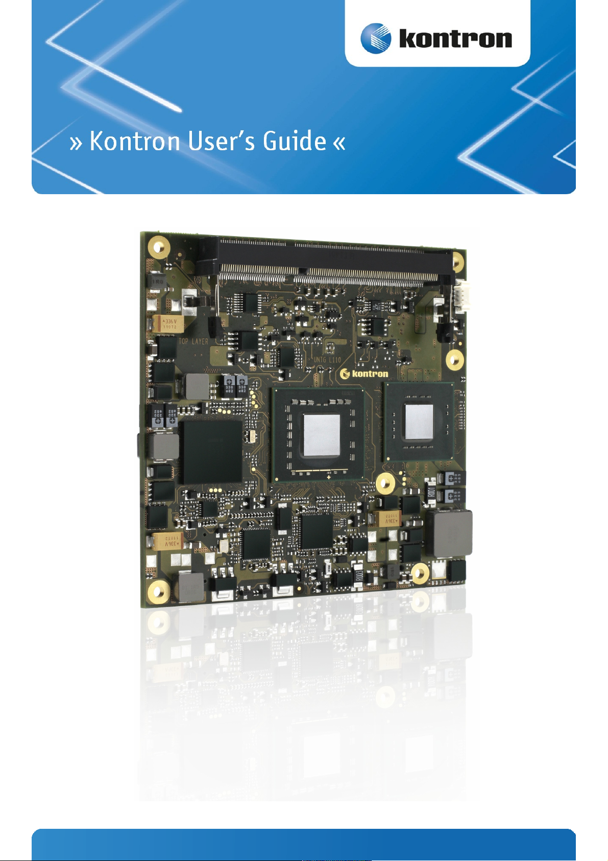
COMe-cPC2
Document Revision 130
www.kontron.com
Page 2

Page 3

» Table of Contents «
1 User Information..................................................................................6
1.1 About This Document.................................................................................................................... 6
1.2 Copyright Notice.......................................................................................................................... 6
1.3 Trademarks................................................................................................................................. 6
1.4 Standards................................................................................................................................... 6
1.5 Warranty.................................................................................................................................... 7
1.6 Technical Support......................................................................................................................... 7
1.7 Naming clarification..................................................................................................................... 7
1.8 Understanding COM Express® Functionality.......................................................................................8
1.9 COM Express® Documentation......................................................................................................... 9
1.10 COM Express® Benefits.................................................................................................................. 9
2 Product Specification..........................................................................10
2.1 Modules & Accessories................................................................................................................. 10
2.2 Functional Specification............................................................................................................... 11
2.3 Block Diagram............................................................................................................................ 15
2.4 Electrical Specification................................................................................................................ 16
2.4.1 Supply Voltage........................................................................................................................... 16
2.4.2 Power Supply Rise Time................................................................................................................ 16
2.4.3 Supply Voltage Ripple.................................................................................................................. 16
2.4.4 Power Consumption..................................................................................................................... 16
2.4.5 ATX Mode.................................................................................................................................. 17
2.4.6 Single Supply Mode..................................................................................................................... 17
2.5 Power Control............................................................................................................................ 18
2.6 Environmental Specification......................................................................................................... 19
2.6.1 Temperature Specification............................................................................................................19
2.6.2 Humidity................................................................................................................................... 19
2.7 Standards and Certifications......................................................................................................... 20
2.8 MTBF........................................................................................................................................ 22
2.9 Mechanical Specification.............................................................................................................. 23
2.10 Module Dimensions..................................................................................................................... 23
2.11 Thermal Management..................................................................................................................24
2.12 Heatspreader............................................................................................................................. 24
2.13 Onboard Fan Connector................................................................................................................ 25
2.13.1 BIOS Settings for Fan Control........................................................................................................ 26
2.13.2 Electrical Characteristics.............................................................................................................. 26
3 Features and Interfaces.......................................................................27
3.1 S5 Eco Mode.............................................................................................................................. 27
3.2 LPC.......................................................................................................................................... 28
3.3 LPC boot................................................................................................................................... 29
3.4 M.A.R.S.................................................................................................................................... 30
3.5 Fast I2C.................................................................................................................................... 31
www.kontron.com
Page 4

COMe-cPC2 /
3.6 JIDA16 and JIDA32..................................................................................................................... 32
3.7 K-Station 1................................................................................................................................ 33
3.8 K-Station & API Resources............................................................................................................ 34
3.8.1 I2C.......................................................................................................................................... 34
3.8.2 Storage.................................................................................................................................... 34
3.8.3 GPIO........................................................................................................................................ 34
3.8.4 Hardware Monitor....................................................................................................................... 34
3.9 GPIO - General Purpose Input and Output.........................................................................................35
3.10 Watchdog Timer.......................................................................................................................... 36
3.11 Flash Backup Feature................................................................................................................... 37
3.12 Speedstep Technology................................................................................................................. 39
3.13 C-States.................................................................................................................................... 40
3.14 Dynamic FSB Frequency Switching.................................................................................................. 41
3.15 VID-x....................................................................................................................................... 42
3.16 Enhanced Intel Dynamic Acceleration Technology..............................................................................43
3.17 Usage of Different Graphic Interfaces..............................................................................................44
3.18 Alternative Pin-out of HDMI.......................................................................................................... 45
3.19 Alternative Pin-out of Display Port.................................................................................................. 45
3.20 Display Configurations.................................................................................................................46
3.21 Hybrid Graphics / Multi-monitor.................................................................................................... 48
3.22 Intel® vPro™ technology.............................................................................................................. 50
3.23 ACPI Suspend Modes and Resume Events..........................................................................................51
4 System Resources...............................................................................52
4.1 Interrupt Request (IRQ) Lines........................................................................................................ 52
4.1.1 In 8259 PIC Mode........................................................................................................................ 52
4.1.2 In APIC mode............................................................................................................................. 53
4.2 Direct Memory Access (DMA) Channels............................................................................................. 53
4.3 Memory Area............................................................................................................................. 53
4.4 I/O Address Map......................................................................................................................... 54
4.5 External Inter-IC (I2C) Bus............................................................................................................54
4.6 System Management (SM) Bus....................................................................................................... 54
4.7 JILI I2C Bus............................................................................................................................... 54
4.8 SDVO I2C Bus............................................................................................................................. 54
4.9 CRT I2C Bus............................................................................................................................... 54
5 Connectors........................................................................................55
5.1 Connector Location..................................................................................................................... 55
5.2 Pinout List................................................................................................................................ 56
5.2.1 General Signal Description............................................................................................................ 56
5.2.2 Connector X1A Row A................................................................................................................... 57
5.2.3 Connector X1A Row B................................................................................................................... 59
5.2.4 Connector X1B Row C................................................................................................................... 61
5.2.5 Connector X1B Row D................................................................................................................... 63
6 BIOS Operation...................................................................................65
6.1 Determining the BIOS Version....................................................................................................... 65
4
Page 5

COMe-cPC2 /
6.2 BIOS Update.............................................................................................................................. 65
6.3 Setup Guide............................................................................................................................... 66
6.3.1 Start AMI® BIOS Setup Utility....................................................................................................... 66
6.4 BIOS Setup................................................................................................................................ 68
6.4.1 Main Menu................................................................................................................................ 68
6.4.2 Module Info............................................................................................................................... 69
6.4.3 Advanced Menu.......................................................................................................................... 72
6.4.4 PCIPnP Menu.............................................................................................................................. 97
6.4.5 Boot........................................................................................................................................ 98
6.4.6 Security.................................................................................................................................... 99
6.4.7 Chipset................................................................................................................................... 100
6.4.8 Exit Menu................................................................................................................................ 106
5
Page 6

COMe-cPC2 / User Information
1 User Information
1.1 About This Document
This document provides information about products from Kontron Europe GmbH and/or its subsidiaries. No warranty of
suitability, purpose, or fitness is implied. While every attempt has been made to ensure that the information in this
document is accurate, the information contained within is supplied “as-is” and is subject to change without notice.
For the circuits, descriptions and tables indicated, Kontron assumes no responsibility as far as patents or other rights of
third parties are concerned.
1.2 Copyright Notice
Copyright © 2003-2012 Kontron Europe GmbH
All rights reserved. No part of this document may be reproduced, transmitted, transcribed, stored in a retrieval system, or
translated into any language or computer language, in any form or by any means (electronic, mechanical, photocopying,
recording, or otherwise), without the express written permission of Kontron Europe GmbH.
DIMM-PC®, PISA®, ETX®, ETXexpress®, microETXexpress®, X-board®, DIMM-IO® and DIMM-BUS® are trademarks or
registered trademarks of Kontron Europe GmbH. Kontron is trademark or registered trademark of Kontron AG.
1.3 Trademarks
The following lists the trademarks of components used in this board.
» IBM, XT, AT, PS/2 and Personal System/2 are trademarks of International Business Machines Corp.
» Microsoft is a registered trademark of Microsoft Corp.
» Intel is a registered trademark of Intel Corp.
» All other products and trademarks mentioned in this manual are trademarks of their respective owners.
1.4 Standards
Kontron Europe GmbH is certified to ISO 9000 standards.
6
Page 7

COMe-cPC2 / User Information
1.5 Warranty
This Kontron Europe GmbH product is warranted against defects in material and workmanship for the warranty period
from the date of shipment. During the warranty period, Kontron Europe GmbH will at its discretion decide to repair or
replace defective products.
Within the warranty period, the repair of products is free of charge as long as warranty conditions are observed.
The warranty does not apply to defects resulting from improper or inadequate maintenance or handling by the buyer,
unauthorized modification or misuse, operation outside of the product’s environmental specifications or improper
installation or maintenance.
Kontron Europe GmbH will not be responsible for any defects or damages to other products not supplied by Kontron
Europe GmbH that are caused by a faulty Kontron Europe GmbH product.
1.6 Technical Support
Technicians and engineers from Kontron Europe GmbH and/or its subsidiaries are available for technical support. We are
committed to making our product easy to use and will help you use our products in your systems.
Please consult our Web site at http://www.kontron.com/support for the latest product documentation, utilities, drivers
and support contacts. Consult our customer section http://emdcustomersection.kontron.com for the latest BIOS
downloads, Product Change Notifications, Board Support Packages, DemoImages, 3D drawings and additional tools and
software. In any case you can always contact your board supplier for technical support.
1.7 Naming clarification
COM Express® defines a Computer-On-Module, or COM, with all components necessary for a bootable host computer,
packaged as a super component.
» COMe-bXX# modules are Kontron's COM Express® modules in basic form factor (125mm x 95mm), formerly known
as ETXexpress®
» COMe-cXX# modules are Kontron's COM Express® modules in compact form factor (95mm x 95mm), formerly known
as microETXexpress®
» COMe-mXX# modules are Kontron's COM Express® modules in mini form factor (55mm x 84mm), formerly known as
nanoETXexpress
The product names for Kontron COM Express® Computer-on-Modules consist of a short form of the industry standard
(COMe-), the form factor (b=basic, c=compact, m=mini), the capital letters for the CPU and Chipset Codenames (XX) and
the pin-out type (#) followed by the CPU Name.
7
Page 8
COMe-cPC2 / User Information
1.8 Understanding COM Express® Functionality
All Kontron COM Express® basic and compact modules contain two 220pin connectors; each of it has two rows called Row
A & B on primary connector and Row C & D on secondary connector. COM Express® Computer-on-modules feature the
following maximum amount of interfaces according to the PICMG module Pin-out type:
Feature Pin-Out Type 1 Pin-Out Type 10 Pin-Out Type 2 Pin-Out Type 6
HD Audio
1x 1x 1x 1x
Gbit Ethernet
1x 1x 1x 1x
Serial ATA
4x 4x 4x 4x
Parallel ATA
- - 1x -
PCI
- - 1x -
PCI Express x1
6x 6x 6x 8x
PCI Express x16 (PEG)
- - 1x 1x
USB Client
1x 1x - -
USB 2.0
8x 8x 8x 8x
USB 3.0
- 2x - 4x
VGA
1x - 1x 1x
LVDS
Dual Channel Single Channel Dual Channel Dual Channel
DP++ (SDVO/DP/HDMI/DVI)
1x optional 1x 3x shared with PEG 3x
LPC
1x 1x 1x 1x
External SMB
1x 1x 1x 1x
External I2C
1x 1x 1x 1x
GPIO
8x 8x 8x 8x
SDIO
1x optional 1x optional - -
UART (2-wire COM)
- 2x - 2x
FAN PWM out
- 1x - 1x
8
Page 9
COMe-cPC2 / User Information
1.9 COM Express® Documentation
This product manual serves as one of three principal references for a COM Express® design. It documents the
specifications and features of COMe-cPC2. Additional references are are available from your Kontron Support or from
PICMG®:
» The COM Express® Specification defines the COM Express® module form factor, pin-out, and signals. This document
is available from the PIGMG website by filling out the order form.
» The COM Express® Design Guide by PICMG serves as a general guide for baseboard design, with a focus on maximum
flexibility to accommodate a wide range of COM Express® modules.
Some of the information contained within this product manual applies only to certain
product revisions (CE: xxx). If certain information applies to specific product revisions (CE:
xxx) it will be stated. Please check the product revision of your module to see if this
information is applicable.
1.10 COM Express® Benefits
COM Express® modules are very compact, highly integrated computers. All Kontron COM Express® modules feature a
standardized form factor and a standardized connector layout that carry a specified set of signals. Each COM is based on
the COM Express® specification. This standardization allows designers to create a single-system baseboard that can
accept present and future COM Express® modules.
The baseboard designer can optimize exactly how each of these functions implements physically. Designers can place
connectors precisely where needed for the application on a baseboard designed to optimally fit a system’s packaging.
A single baseboard design can use a range of COM Express® modules with different size and pin-out. This flexibility can
differentiate products at various price/performance points, or to design future proof systems that have a built-in upgrade
path. The modularity of a COM Express® solution also ensures against obsolescence as computer technology evolves. A
properly designed COM Express® baseboard can work with several successive generations of COM Express® modules.
A COM Express® baseboard design has many advantages of a custom, computer-board design but delivers better
obsolescence protection, greatly reduced engineering effort, and faster time to market.
9
Page 10
COMe-cPC2 / Product Specification
2 Product Specification
2.1 Modules & Accessories
The COM Express® compact sized Computer-on-Module COMe-cPC2 (UNTG) follows pin-out Type 2 and is compatible to
PICMG specification COM.0 Rev 1.0. The COMe-cPC2, based on Intel's Montevina platform, is available in different variants
to cover the demand of different performance, price and power:
Commercial grade modules (0°C to 60°C operating)
Product Number Product Name Processor Socket GMCH IOH
36004-0000-23-2 COMe-cPC2 SP9300 Intel® Core™2 Duo SP9300 BGA956 GS45 ICH9M-SFF
36004-0000-19-2 COMe-cPC2 SL9400 Intel® Core™2 Duo SL9400 BGA956 GS45 ICH9M-SFF
36004-0000-12-2 COMe-cPC2 SU9300 Intel® Core™2 Duo SU9300 BGA956 GS45 ICH9M-SFF
36004-0000-12-3 COMe-cPC2 CM723 Intel® Celeron®M ULV 723 BGA956 GS45 ICH9M-SFF
36004-0000-12-1 COMe-cPC2 CM722 Intel® Celeron®M ULV 722 BGA956 GS45 ICH9M-SFF
Accessories
Product Number Carrier Boards
38102-0000-00-1 COM Express® Reference Carrier Type 2 (8mm COMe connector)
38104-0000-00-0 COM Express® Eval Carr ier Type 2 (Niles Canyon, 5mm COMe connector)
38104-0000-00-1 COM Express® Eval Carr ier Type 2 (Topanga Canyon, 5mm COMe connector)
Product Number Memory
97015-1024-10-0 DDR3-1066 SODIMM 1GB
97015-2048-10-0 DDR3-1066 SODIMM 2GB
97015-4096-10-0 DDR3-1066 SODIMM 4GB
Product Number Cooling & Mounting
36004-0000-99-0 HSP COMe-cPC2 thread
36004-0000-99-1 HSP COMe-cPC2 through
36004-0000-99-0C01 HSK COMe-cPC2 active thread
36004-0000-99-0C02 HSK COMe-cPC2 passive thread
36099-0000-99-0 COMe Active Uni Cooler (for CPUs up to 20W TDP)
36099-0000-99-1 COMe Passive Uni Cooler (for CPUs up to 10W TDP)
38017-0000-00-0 COMe Mount KIT 8mm 1set
38017-0000-00-5 COMe Mount KIT 5mm 1set
38017-0100-00-0 COMe Mount KIT 8mm 100sets
38017-0100-00-5 COMe Mount KIT 5mm 100sets
Product Number Adapter & Cables
9-5000-0352 ADA-LVDS-DVI 18bit (LVDS to DVI converter)
9-5000-0353 ADA-LVDS-DVI 24bit (LVDS to DVI converter)
96006-0000-00-7 ADA-Type2-DP3 (Adapter Card Type 2 module to 3x DisplayPort)
96006-0000-00-8 ADA-DP-LVDS (DP to LVDS adapter)
96082-0000-00-0 KAB-ADAPT-DP-DVI (DP to DVI adapter cable)
96083-0000-00-0 KAB-ADAPT-DP-VGA (DP to VGA adapter cable)
96084-0000-00-0 KAB-ADAPT-DP-HDMI (DP to HDMI adapter cable)
96079-0000-00-0 KAB-HSP 200mm (Cable adapter to connect FAN to module)
96079-0000-00-2 KAB-HSP 40mm (Cable adapter to connect FAN to module)
10
Page 11
COMe-cPC2 / Product Specification
2.2 Functional Specification
Processor
The Intel® Core™ Duo / Celeron® (Penryn) CPU family supports:
» Intel® Dynamic Acceleration (Turbo Mode)
» Intel® Virtualization Technology (VT-x)
» Intel® Trusted Execution Technology (TXT)
» Intel® 64
» Idle States
» Enhanced Intel SpeedStep® Technology
» Execute Disable Bit
» Intel® Dynamic FSB Frequency Switching (SuperLFM)
» Thermal Monitoring Technologies
CPU specifications
Processor Cores Core CPU Clock Turbo L2 Cache C-States FSB Speed V T-x TXT Intel® 64 EIST
Intel® Celeron® M722 1 45nm Penryn 1200MHz - 3MB C0 - C3 800 MHz No No Yes No
Intel® Celeron® M723 1 45nm Penryn 1200MHz - 1MB C0 - C3 800 MHz No No Yes No
Intel® Core™2 Duo SU9300 2 45nm Penryn 1200MHz 1400MHz 3MB C0 - C6 800 MHz Yes Yes Yes Yes
Intel® Core™2 Duo SL9400 2 45nm Penryn 1866MHz 2000MHz 6MB C0 - C6 1066 MHz Yes Yes Yes Yes
Intel® Core™2 Duo SP9300 2 45nm Penryn 2266MHZ 2400MHz 6MB C0 - C6 1066 MHz Yes Yes Yes Yes
Chipset
The Intel Gen4 Graphics and Memory Controller Hub Cantiga supports:
» PCI Express Revision 1.1
» Intel® Virtualization Technology for Directed I/O (VT-d)
» Intel® Trusted Execution Technology
» Intel® Active Management Technology 4.0
» Intel® ICH9 family IO Controller
IOH specifications
» 2.5W TDP
» integrated Trusted Platform Module (iTPM)
» SATA RAID
The Intel® Trusted Execution Technology (TXT) and Active Management Technology (AMT)
are not supported by default on COMe-cPC2. Please contact your local sales or support.
11
Page 12

COMe-cPC2 / Product Specification
Memory
Sockets
1x DDR3 SO-DIMM
Memory Type
DDR3-667/800/1066
Maximum Size
4GB
Technology
Single Channel
Graphics Core
The integrated Intel® GMA X4500MHD (Gen5.5) supports:
Graphics Core Render Clock
533/320MHz, ,
Execution Units / Pixel Pipelines
10
Max Graphics Memory
1700MB
GFX Memory Bandwidth (GB/s)
17
GFX Memory Technology
DVMT 5.0
API (DirectX/OpenGL)
10 / 2.1
Shader Model
4.0
Hardware accelerated Video
MPEG2, VC-1, AVC, Blu-ray
Independent/Simultaneous Displays
2
Display Port
YES
HDCP support
HDCP 1.2 (Keys optional)
Monitor output
CRT max Resolution
2048x1536
TV out:
YES
LVDS
LVDS Bits/Pixel
1x18 / 2x18
LVDS Bits/Pixel with dithering
1x24 / 2x24
LVDS max Resolution:
1600x1200
PWM Backlight Control:
YES
Supported Panel Data:
JILI2/JILI3/EDID/DID
Display Interfaces
Discrete Graphics
1x PEG 1.0
Digital Display Interface DDI1
DP++/SDVOB
Digital Display Interface DDI2
DP++/SDVOC
Digital Display Interface DDI3
DP++
Maximum Resolution on DDI
2560x1600
The discrete PEG graphics port and the digitial display interfaces are multiplexed and
cannot be used simultaneously. Display Port plus plus (DP++) allows usage as DisplayPort,
HDMI or DVI
PEG Configuration
The x16 PCI Express Graphics Port (PEG) is compatible to standard PCI Express devices like Ethernet or RAID controllers.
The COMe-cPC2 supports following PEG Port configuration when used as PCI Express Interface:
» 1×16
» 1×8
» 1×4
» 1×1
12
Page 13

COMe-cPC2 / Product Specification
Storage
onboard SSD
-
SD Card support
-
IDE Interface
JMD330 SATA#3 to PATA
Serial-ATA
3x SATA 3Gb/s
SATA AHCI
NCQ, HotPlug, Staggered Spinup, eSATA, PortMultiplier
SATA RAID
0, 1
Connectivity
USB
8x USB 2.0
USB Client
-
PCI
PCI Rev 2.3 (33MHz/3.3V)
PCI External Masters
4
PCI Express
5x PCIe x1 Gen1
Max PCI Express
6x PCIe x1 without LAN
PCI Express x2/x4 configuration
YES
Ethernet
10/100/1000 Mbit
Ethernet controller
Intel® 82567 (Boazman)
It is also possible to run the 1st 4 x1 lanes as 1 x4 lane. For that please pull-up the signal A33 and A29 to 3.3V on the
baseboard.
Express Card hotplug functionality is only available, when in BIOS setup the PCIexpress
lane is switched from [AUTO] to [ENABLED]
Ethernet
The Intel® 82567 (Boazman) ethernet supports:
» Jumbo Frames
» MACsec IEEE 802.1 AE
» WOL (Wake On LAN)
» PXE (Preboot eXecution Environment)
Misc Interfaces and Features
Audio
HD Audio
Onboard Hardware Monitor
ON Semi ADT7475
Trusted Platform Module
iTPM 1.2 (integrated in ICH9M)
Miscellaneous
-
Kontron Features
External I2C Bus
Fast I2C
M.A.R.S. support
YES
Embedded API
JIDA16 / JIDA32 / PICMG EAPI
Custom BIOS Settings / Flash Backup
YES
Watchdog support
Single Staged
Power Features
Singly Supply Support
YES
Supply Voltage
8.5V - 18V
ACPI
ACPI 3.0
S-States
S0, S3, S4, S5
S5 Eco Mode
YES
Misc Power Management
DPST 4.3
13
Page 14

COMe-cPC2 / Product Specification
Power Consumption and Performance
Full Load Power Consumption
13.5 - 43W
Kontron Performance Index
2899 - 5769
Kontron Performance/Watt
133 - 214
Detailed Power Consumption measurements in all states and bechmarks for CPU, Graphics
and Memory performance are available in Application Note KEMAP054 at EMD Customer
Section.
Supported Operating Systems
The COMe-cPC2 supports:
» Microsoft Windows XP x86/x64
» Microsoft Windows Vista x86/x64
» Microsoft Windows 7 x86/x64
» Microsoft Windows CE 6.0
» Microsoft Windows XP embedded
» Linux
» WindRiver VxWorks
» QNX Neutrino
14
Page 15
COMe-cPC2 / Product Specification
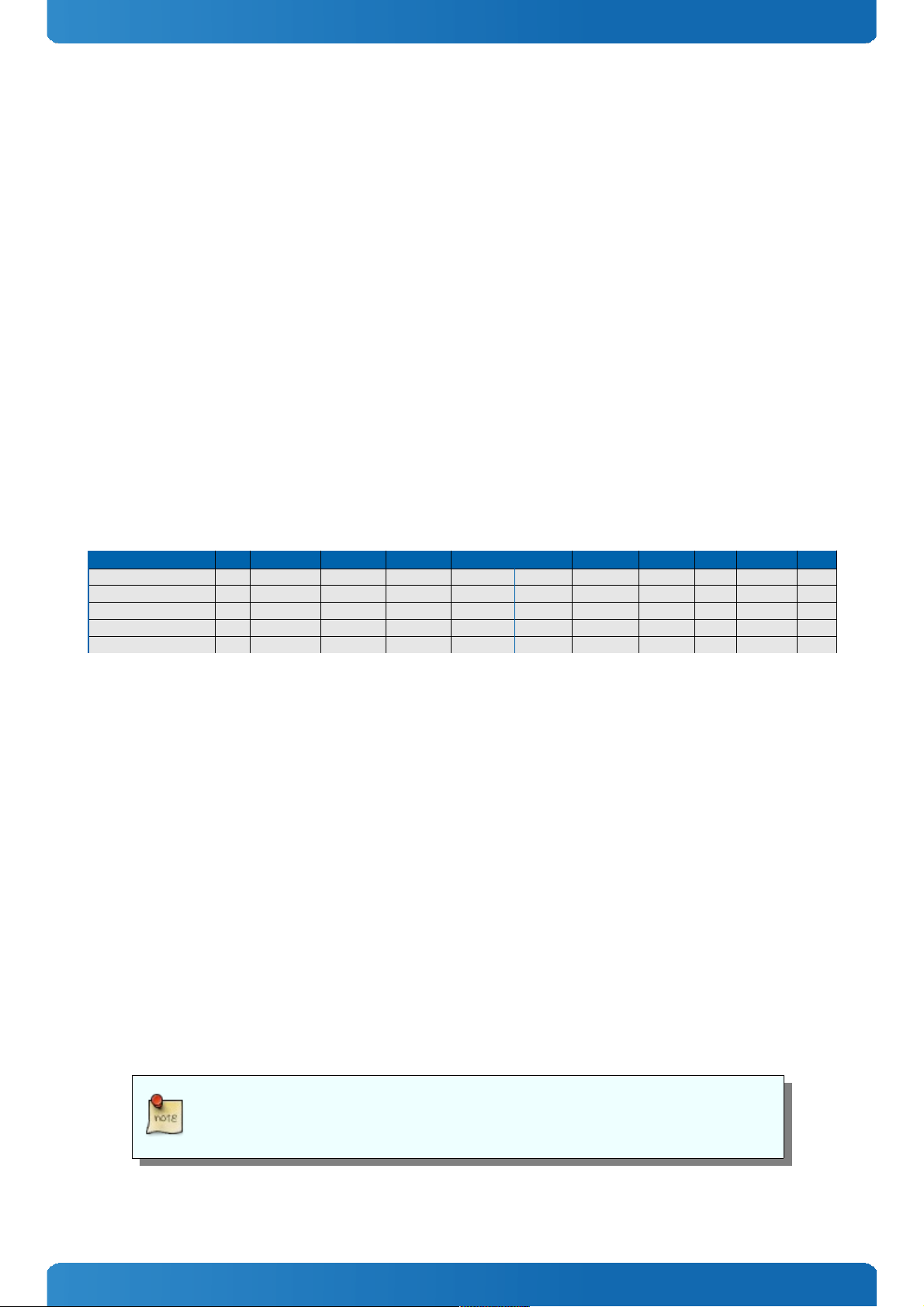
2.3 Block Diagram
15
Page 16

COMe-cPC2 / Product Specification
2.4 Electrical Specification
2.4.1 Supply Voltage
Following supply voltage is specified at the COM Express® connector:
VCC:
8.5V - 18V
Standby:
5V DC +/- 5%
RTC:
2.5V - 3.3V
- 5V Standby voltage is not mandatory for operation.
- Extended Temperature (E1) variants are validated for 12V supply only
2.4.2 Power Supply Rise Time
» The input voltages shall rise from ≤10% of nominal to within the regulation ranges within 0.1ms to 20ms.
» There must be a smooth and continuous ramp of each DC input voltage from 10% to 90% of its final set-point
following the ATX specification
2.4.3 Supply Voltage Ripple
» Maximum 100 mV peak to peak 0 – 20 MHz
2.4.4 Power Consumption
The maximum Power Consumption of the different COMe-cPC2 variants is 13.5 - 43W (100% CPU load on all cores; 90°C
CPU temperature). Further information with detailed measurements are available in Application Note KEMAP054 available
on EMD Customer Section. Information there is available after registration.
16
Page 17
COMe-cPC2 / Product Specification
2.4.5 ATX Mode
By connecting an ATX power supply with VCC and 5VSB, PWR_OK is set to low level and VCC is off. Press the Power Button to
enable the ATX PSU setting PWR_OK to high level and powering on VCC. The ATX PSU is controlled by the PS_ON# signal
which is generated by SUS_S3# via inversion. VCC can be 8.5V - 18V in ATX Mode. On Computer-on-Modules supporting a
wide range input down to 4.75V the input voltage shall always be higher than 5V Standby (VCC > 5VSB).
State PWRBTN# PWR_OK V5_StdBy PS_ON# VCC
G3 x x 0V x 0V
S5 high low 5V high 0V
S5 S0 → PWRBTN Event low high → 5V high low → 0 V VCC →
S0 high high 5V low VCC
2.4.6 Single Supply Mode
In single supply mode (or automatic power on after power loss) without 5V Standby the module will start automatically
when VCC power is connected and Power Good input is open or at high level (internal PU to 3.3V). PS_ON# is not used in
this mode and VCC can be 8.5V - 18V.
To power on the module from S5 state press the power button or reconnect VCC. Suspend/Standby States are not
supported in Single Supply Mode.
State PWRBTN# PWR_OK V5_StdBy VCC
G3 x x x 0
G3 S0 → high open / high x connecting VCC
S5 high open / high x VCC
S5 S0 → PWRBTN Event open / high x reconnecting VCC
Signals marked with “x” are not important for the specific power state. There is no
difference if connected or open.
All ground pins have to be tied to the ground plane of the carrier board.
17
Page 18
COMe-cPC2 / Product Specification
2.5 Power Control
Power Supply
The COMe-cPC2 supports a power input from 8.5V - 18V. The supply voltage is applied through the VCC pins (VCC) of the
module connector.
Power Button (PWRBTN#)
The power button (Pin B12) is available through the module connector described in the pinout list. To start the module via
Power Button the PWRBTN# signal must be at least 50ms (50ms ≤ t < 4s, typical 400ms) at low level (Power Button Event).
Pressing the power button for at least 4seconds will turn off power to the module (Power Button Override).
Power Good (PWR_OK)
The COMe-cPC2 provides an external input for a power-good signal (Pin B24). The implementation of this subsystem
complies with the COM Express® Specification. PWR_OK is internally pulled up to 3.3V and must be high level to power on
the module.
Reset Button (SYS_RESET#)
The reset button (Pin B49) is available through the module connector described in the pinout list. The module will stay in
reset as long as SYS_RESET# is grounded. If available, the BIOS setting for “Reset Behavior” must be set to “Power Cycle”.
Modules with Intel® Chipset and active Management Engine does not allow to hold the
module in Reset out of S0 for a long time. At about 10s holding the reset button the ME will
reboot the module automatically
SM-Bus Alert (SMB_ALERT#)
With an external battery manager present and SMB_ALERT# (Pin B15) connected the module always powers on even if
BIOS switch “After Power Fail” is set to “Stay Off”.
18
Page 19
COMe-cPC2 / Product Specification
2.6 Environmental Specification
2.6.1 Temperature Specification
General Specification Operating Non-operating
Commercial grade 0°C to +60°C -30°C to +85°C
Extended (E1) -25°C to +75°C -30°C to +85°C
Industrial grade (E2) -40°C to +85°C -40°C to +85°C
Standard modules are available for commercial grade temperature range. Please see
chapter Product Specification for available variants for extended or industrial temperate
grade
With Kontron heatspreader plate assembly
The operating temperature defines two requirements:
» the maximum ambient temperature with ambient being the air surrounding the module.
» the maximum measurable temperature on any spot on the heatspreader's surface
Without Kontron heatspreader plate assembly
The operating temperature is the maximum measurable temperature on any spot on the module's surface.
2.6.2 Humidity
» Operating: 10% to 90% (non condensing)
» Non operating: 5% to 95% (non condensing)
19
Page 20
COMe-cPC2 / Product Specification
2.7 Standards and Certifications
RoHS
The COMe-cPC2 is compliant to the directive 2002/95/EC on the restriction of the use of certain hazardous substances
(RoHS) in electrical and electronic equipment.
CE marking
The COMe-cPC2 is CE marked according to Low Voltage Directive 2006/95/EC – Test standard EN60950
Component Recognition UL 60950-1
The COM Express® compact form factor Computer-on-Modules are Recognized by Underwriters Laboratories Inc.
Representative samples of this component have been evaluated by UL and meet applicable UL requirements.
UL Listings:
» NWGQ2.E304278
» NWGQ8.E304278
WEEE Directive
WEEE Directive 2002/96/EC is not applicable for Computer-on-Modules.
Conformal Coating
Conformal Coating is available for Kontron Computer-on-Modules and for validated SO-DIMM memory modules. Please
contact your local sales or support for further details.
20
Page 21

COMe-cPC2 / Product Specification
Shock & Vibration
The COM Express® compact form factor Computer-on-Modules successfully passed shock and vibration tests according to
» IEC/EN 60068-2-6 (Non operating Vibration, sinusoidal, 10Hz-4000Hz, +/-0.15mm, 2g)
» IEC/EN 60068-2-27 (Non operating Shock Test, half-sinusoidal, 11ms, 15g)
EMC
Validated in Kontron reference housing for EMC the COMe-cPC2 follows the requirements for electromagnetic
compatibility standards
» EN55022
» EN55011
» EN55024
» FCC15
21
Page 22
COMe-cPC2 / Product Specification
2.8 MTBF
The following MTBF (Mean Time Before Failure) values were calculated using a combination of manufacturer’s test data, if
the data was available, and the Telcordia (Bellcore) issue 2 calculation for the remaining parts.
The calculation methode used is “Telcordia Method 1 Case 3” in a ground benign, controlled environment (GB,GC). This
particular method takes into account varying temperature and stress data and the system is assumed to have not been
burned in.
Other environmental stresses (extreme altitude, vibration, salt water exposure, etc) lower MTBF values.
System MTBF (hours): 175488 @ 40°C
Fans usually shipped with Kontron Europe GmbH products have 50,000-hour typical
operating life. The above estimates assume no fan, but a passive heat sinking arrangement
Estimated RTC battery life (as opposed to battery failures) is not accounted for in the above
figures and need to be considered for separately. Battery life depends on both temperature
and operating conditions. When the Kontron unit has external power; the only battery
drain is from leakage paths.
22
Page 23
COMe-cPC2 / Product Specification
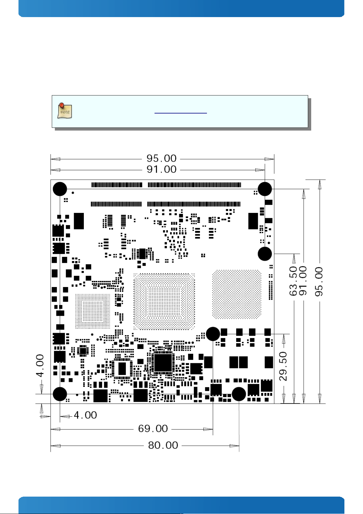
2.9 Mechanical Specification
Dimension
» 95.0 mm x 95.0 mm (3.75” x 3.75”)
» Hight approx. 12mm (0.4”)
CAD drawings are available at EMD CustomerSection
2.10 Module Dimensions
23
Page 24

COMe-cPC2 / Product Specification
2.11 Thermal Management
A heatspreader plate assembly is available from Kontron Europe GmbH for the COMe-cPC2. The heatspreader plate on top
of this assembly is NOT a heat sink. It works as a COM Express®-standard thermal interface to use with a heat sink or other
cooling device.
External cooling must be provided to maintain the heatspreader plate at proper operating temperatures. Under worstcase conditions, the cooling mechanism must maintain an ambient air and heatspreader plate temperature of 60° C or
less.
The aluminum slugs and thermal pads on the underside of the heatspreader assembly implement thermal interfaces
between the heatspreader plate and the major heat-generating components on the COMe-cPC2. About 80 percent of the
power dissipated within the module is conducted to the heatspreader plate and can be removed by the cooling solution.
You can use many thermal-management solutions with the heatspreader plates, including active and passive approaches.
The optimum cooling solution varies, depending on the COM Express® application and environmental conditions. Please
see the COM Express® Design Guide for further information on thermal management.
2.12 Heatspreader
Documentation and CAD drawings of COMe-cPC2 heatspreader and cooling solutions is provided at
http://emdcustomersection.kontron.com.
24
Page 25
COMe-cPC2 / Product Specification
2.13 Onboard Fan Connector
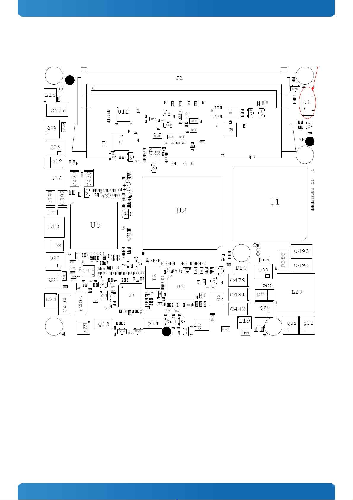
Location and Pinout of Fan Connector
The onboard fan connector (J1) can be found at the right side nearby the DRAM socket. Use adaptor KAB-HSP (960790000-00-0) to connect a standard FAN.
Connector J1 has following specification:
» Part number (Molex) J8: 53261-0390
» Mates with: 51021-0300
» Crimp terminals: 50079-8100
The Pin assignement is:
» Pin1: Tacho
» Pin2: VCC
» Pin3: GND
25
Page 26
COMe-cPC2 / Product Specification
2.13.1 BIOS Settings for Fan Control
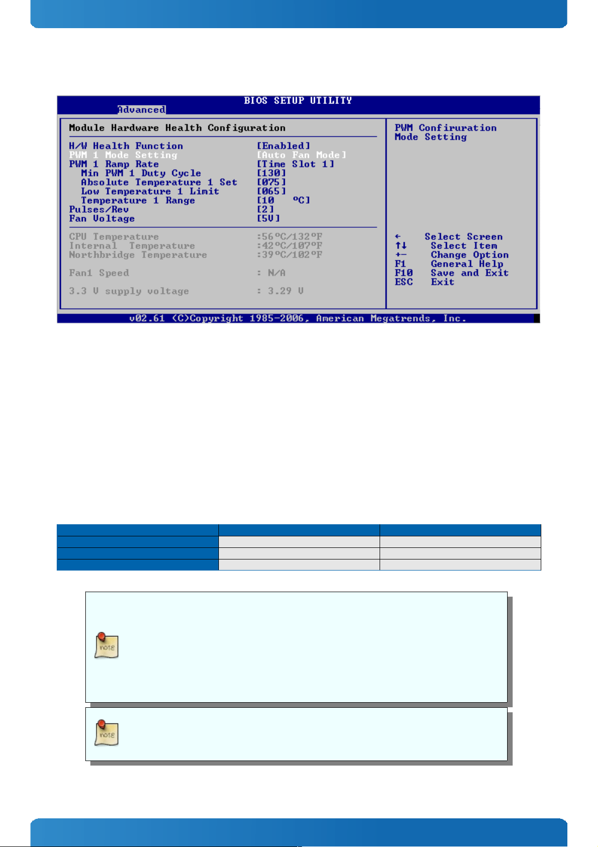
The fan can be controlled via the BIOS Settings “Advanced Hardware Health Module Hardware Health”→ →
In general 4 modes are possible
» Auto Fan Mode: Temperature Values can be selected to control the Fan
» Fan Always On Full: Fan is always full on
» Fan Disable Mode: Fan is disabled
» Fan Manually Mode: A fixed PWM value (0…255) can be entered to run the fan at a selected speed
The used hardware monitor onboard is an ADT7475. For additional information please refer to the regarding datasheet.
2.13.2 Electrical Characteristics
There are 2 version of onboard fan control possible. Our standard modules have the simple version populated. For custom
projects it is possible to populate a more sophisticated one. The differences are:
Features Premium Fan Base Fan
Input Voltage Range
8.5V - 18V 8.5V - 18V
Output Voltage
5V / 12V Only 12V (switch in BIOS without function)
Max. output current
1A 0.3A
The fan voltage is in both versions VCC of the board and limited to 12V max.
The Fan out voltage output is not short circuit proof. If necessary the user has to ensure
that the circuit is protected externally, for example by a fuse on the backplane.
With premium fan solution it is recommended to select the correct fan voltage first in BIOS
setup and then connect the fan.
To connect a standard FAN with 3pin connector to the module please use adaptor cable
KAB-HSP 200mm (96079-0000-00-0) or KAB-HSP 40mm (96079-0000-00-2)
26
Page 27

COMe-cPC2 / Features and Interfaces
3 Features and Interfaces
3.1 S5 Eco Mode
Kontron’s new high-efficient power-off state S5 Eco enables lowest power-consumption in soft-off state – less than 1 mA
compared to the regular S5 state this means a reduction by at least factor 200!
In the “normal” S5 mode the board is supplied by 5V_Stb and needs usually up to 300mA just to stay off. This mode allows
to be switched on by power button, RTC event and WakeOnLan, even when it is not necessary. The new S5 Eco mode
reduces the current tremendously.
The S5 Eco Mode can be enabled in BIOS Setup, when the BIOS supports this feature.
Following prerequesites and consequences occur when S5 Eco Mode is enabled
» The power button must be pressed at least for 200ms to switch on.
» Wake via Powerbutton only.
» “Power On After Power Fail”/“State after G3”: only “stay off” is possible
27
Page 28
COMe-cPC2 / Features and Interfaces
3.2 LPC
The Low Pin Count (LPC) Interface signals are connected to the LPC Bus bridge located in the CPU or chipset. The LPC low
speed interface can be used for peripheral circuits such as an external Super I/O Controller, which typically combines
legacy-device support into a single IC. The implementation of this subsystem complies with the COM Express®
Specification. Implementation information is provided in the COM Express® Design Guide maintained by PICMG. Please
refer to the official PICMG documentation for additional information.
The LPC bus does not support DMA (Direct Memory Access) and a clock buffer is required when more than one device is
used on LPC. This leads to limitations for ISA bus and SIO (standard I/O´s like Floppy or LPT interfaces) implementations.
All Kontron COM Express® Computer-on-Modules imply BIOS support for following external baseboard LPC Super I/O
controller features for the Winbond/Nuvoton 5V 83627HF/G and 3.3V 83627DHG-P:
83627HF/G Phoenix BIOS AMI CORE8 AMI Aptio
PS/2 YES YES YES
COM1/COM2 YES YES YES
LPT YES YES YES
HWM YES YES NO
Floppy NO NO NO
GPIO NO NO NO
83627DHG-P Phoenix BIOS AMI CORE8 AMI Aptio
PS/2 YES YES YES
COM1/COM2 YES YES YES
LPT YES YES YES
HWM NO NO NO
Floppy NO NO NO
GPIO NO NO NO
Features marked as not supported do not exclude OS support (e.g. HWM can be accessed via SMB). For any other LPC
Super I/O additional BIOS implementations are necessary. Please contact your local sales or support for further details.
28
Page 29
COMe-cPC2 / Features and Interfaces
3.3 LPC boot
The COMe-cPC2 supports boot from an external Firmwarehub on LPC bus (LPC FWH). The external LPC FWH can be activated
with signal A34 “BIOS_DISABLE#” or according newer specifications “BIOS_DIS0#” in following configuration:
BIOS_DIS0# BIOS_DIS1# Function
open open Boot on-module BIOS
GND open Boot baseboard LPC FWH
open GND Baseboard SPI = Boot Device 1, on-module SPI = Boot Device 2
GND GND Baseboard SPI = Boot Device 2, on-module SPI = Boot Device 1
Using an external LPC Firmware Hub
To program an external LPC FWH follow these steps:
» Connect a 1MB LPC FWH to the module's LPC interface
» Open pin A34 to boot from the module BIOS
» Boot the module to DOS with access to the BIOS image and Firmware Update Utility aufdos.exe / batch file provided
on EMD Customer Section
» Connect pin A43 (BIOS_DIS0#) to ground to enable the external LPC FWH
» Execute Flash.bat to flash the BIOS image to the external LPC FWH
» reboot
Your module will now boot from the external LPC FWH when BIOS_DIS0# is grounded.
To create a BIOS with custom defaults:
» Change your BIOS settings
» Save as custom defaults to RTC/Flash and Exit (module will now always start with these settings)
» Extract the BIOS including custom defaults with afudos.exe biosname.rom /O in DOS or kflash.exe backup
biosname.rom in Windows
Flash Backup should show “Enter new Password” first time saving custom defaults. If it is
not possible to set a new password or entering a password shows an error message, please
clean up CMOS data with DOS command: jidacmos rtc /clean (jidacmos utility is available
at Kontron’s Customer Section)
You can download all AMI CORE8 update utilities at AMI.com:
http://www.ami.com/support/downloads/amiflash.zip
29
Page 30

COMe-cPC2 / Features and Interfaces
3.4 M.A.R.S.
The Smart Battery implementation for Kontron Computer-on-Modules called Mobile Application for Rechargeable Systems
is a BIOS extension for external Smart Battery Manager or Charger. It includes support for SMBus charger/selector (e.g.
Linear Technology LTC1760 Dual Smart Battery System Manager) and provides ACPI compatibility to report battery
information to the Operating System.
Reserved SM-Bus addresses for Smart Battery Solutions on the carrier:
8-bit Address 7-bit Address Device
12h 0x09 SMART_CHARGER
14h 0x0A SMART_SELECTOR
16h 0x0B SMART_BATTERY
30
Page 31

COMe-cPC2 / Features and Interfaces
3.5 Fast I2C
The COMe-cPC2 supports a CPLD implemented LPC to I2C bridge using the WISHBONE I2C Master Core provided from
opencores.org. The I2C Interface supports transfer rates up to 40kB/s and can be configured in Setup
Specification for external I2C:
» Speed up to 400kHz
» Compatible to Philips I2C bus standard
» Multi-Master capable
» Clock stretching support and wait state generation
» Interrupt or bit-polling driven byte-by-byte data-transfers
» Arbitration lost interrupt with automatic transfer cancellation
» Start/Stop signal generation/detection
» Bus busy detection
» 7bit and 10bit addressing
31
Page 32

COMe-cPC2 / Features and Interfaces
3.6 JIDA16 and JIDA32
JIDA16 (JUMPtec® Intelligent Device Architecture) is a BIOS interface which allows programs running in Real Mode
operating systems (i.e. MS DOS) to call certain functions implemented in the BIOS. These functions can be used to get
module information, make settings and access the I2C Bus and the Watchdog unit. JIDA16 functions are INT 15h BIOS calls
which are only available in 16 Bit Real Mode operating systems.
For 32bit operating systems (i.e. WindowsXP, Windows 7, Windows CE, VxWorks, Linux) a different JIDA implementation
called JIDA32 is implemented. The same common driver for all JIDA32 capable modules talks to the JIDA32 part in the
BIOS, which is hardware dependent to interact with the hardware.
Please refer to EMD Customer Section for detailed documentation, JIDA utilities and Libraries for DOS, Windows, Linux,
VxWorks or QNX.
Usage of JIDA16 and JIDA32
32
Page 33

COMe-cPC2 / Features and Interfaces
3.7 K-Station 1
Based on the JIDA32 interface users can implement advanced board functionality in their application. As an example
utility Kontron provides K-Station for most 32bit Windows Operating Systems. K-Station 1 is a summary of command line
utilities (Shell Tools) for easy access to JIDA32 BIOS implementations. Second part of K-Station is a JAVA based example
GUI which gives a view an all available features using the Shell Tools.
Following K-Station Shell Tools are available:
» KSystemSummary.exe (System Information)
» KGenInfo.exe (Module Information)
» KCPUPerf.exe (CPU Throttling control)
» KHWMon.exe (Hardware Monitoring)
» KI2CBus.exe (I2C and SMBus access)
» KIOPort.exe (GPIO control)
» KStorage.exe (JIDA EEPROM access to user bytes)
» KVGATool.exe (LVDS Backlight control)
» KWDog.exe (Watchdog control)
» KAMIMod.exe (AMICore8 BIOS Modification with Bootlogo or Usercode …)
» KFlash.exe (AMICore8 BIOS Update)
The full K-Station package, the stand-alone Shell Tools with drivers, example batch files and documentation is available
on EMD Customer Section for free.
33
Page 34
COMe-cPC2 / Features and Interfaces
3.8 K-Station & API Resources
3.8.1 I2C
BUS Function
I2C 0 Internal / JIDA I2C
I2C 1 SM-Bus
I2C 2 external I2C
I2C 3 internal watchdog
I2C 4 SDVO DDC
I2C 5 CRT DDC
I2C 6 JILI DDC
3.8.2 Storage
Device Function
EEPROM 0 JIDA EEPROM Area1 with 32 Bytes (free to use)
3.8.3 GPIO
Port Function
IO-Port 0 GPI 0
IO-Port 1 GPI 1
IO-Port 2 GPI 2
IO-Port 3 GPI 3
IO-Port 4 GPO 0
IO-Port 5 GPO 1
IO-Port 6 GPO 2
IO-Port 7 GPO 3
3.8.4 Hardware Monitor
Sensor Function
Temp 0 CPU ACPI Temperature
Temp 1 Internal HWM Temperature (inside ADT7476)
Temp 2 Chipset Temperature (Intel® 4 series chipset)
Temp 3 External SIO Winbond 83627 Temp Sensor 0
Temp 3 External SIO Winbond 83627 Temp Sensor 1
Temp 5 External SIO Winbond 83627 Temp Sensor 2
FAN 0 CPU fan controlled by ADT7476
FAN 1 External SIO Winbond 83627 FAN Sensor 0
FAN 2 External SIO Winbond 83627 FAN Sensor 1
FAN 3 External SIO Winbond 83627 FAN Sensor 2
Voltage 0 Internal ADT7476 Battery Voltage: VBAT
Voltage 1 Internal ADT7476 Supply Voltage: VCC
Voltage 2 External SIO Winbond 83627 CPU Core Voltage Sensor: VCoreA
Voltage 3 External SIO Winbond 83627 CPU Core Voltage Sensor: VCoreB
Voltage 4 External SIO Winbond 83627 Battery Voltage Sensor: VBAT
Voltage 5 External SIO Winbond 83627 Voltage Sensor 3: +3.3V
Voltage 6 External SIO Winbond 83627 Voltage Sensor 4: +5V
Voltage 7 External SIO Winbond 83627 Voltage Sensor 5: +5VSB
Voltage 8 External SIO Winbond 83627 Voltage Sensor 6: +12V
Voltage 9 External SIO Winbond 83627 Voltage Sensor 7: -5V
Voltage 10 External SIO Winbond 83627 Voltage Sensor 8: -12V
Resources based on BIOS revision CNTGR415
34
Page 35

COMe-cPC2 / Features and Interfaces
3.9 GPIO - General Purpose Input and Output
The COMe-cPC2 offers 4 General Purpose Input (GPI) pins and 4 General Purpose Output (GPO) pins. On a 3.3V level digital
in- and outputs are available.
Signal Pin Description
GPI0 A54 General Purpose Input 0
GPI1 A63 General Purpose Input 1
GPI2 A67 General Purpose Input 2
GPI3 A85 General Purpose Input 3
GPO0 A93 General Purpose Output 0
GPO1 B54 General Purpose Output 1
GPO2 B57 General Purpose Output 2
GPO3 B63 General Purpose Output 3
Configuration
The GPI and GPO pins can be configured via JIDA32/K-Station. Please refer to the JIDA32/K-Station manual in the driver
download packet on our customer section.
35
Page 36

COMe-cPC2 / Features and Interfaces
3.10 Watchdog Timer
You can configure the Watchdog Timer (WDT) in BIOS setup to start after a set amount of time after power-on boot. The
WDT can also be controlled by the JIDA32 Library API. The application software should strobe the WDT to prevent its
timeout. Upon timeout, the WDT resets and restarts the system. This provides a way to recover from program crashes or
lockups.
Configuration
You can program the timeout period for the watchdog timer in two ranges:
» 1-second increments from 1 to 255 seconds
» 1-minute increments from 1 to 255 minutes
Contact Kontron Embedded Modules technical support for information on programming and operating the WDT.
36
Page 37
COMe-cPC2 / Features and Interfaces
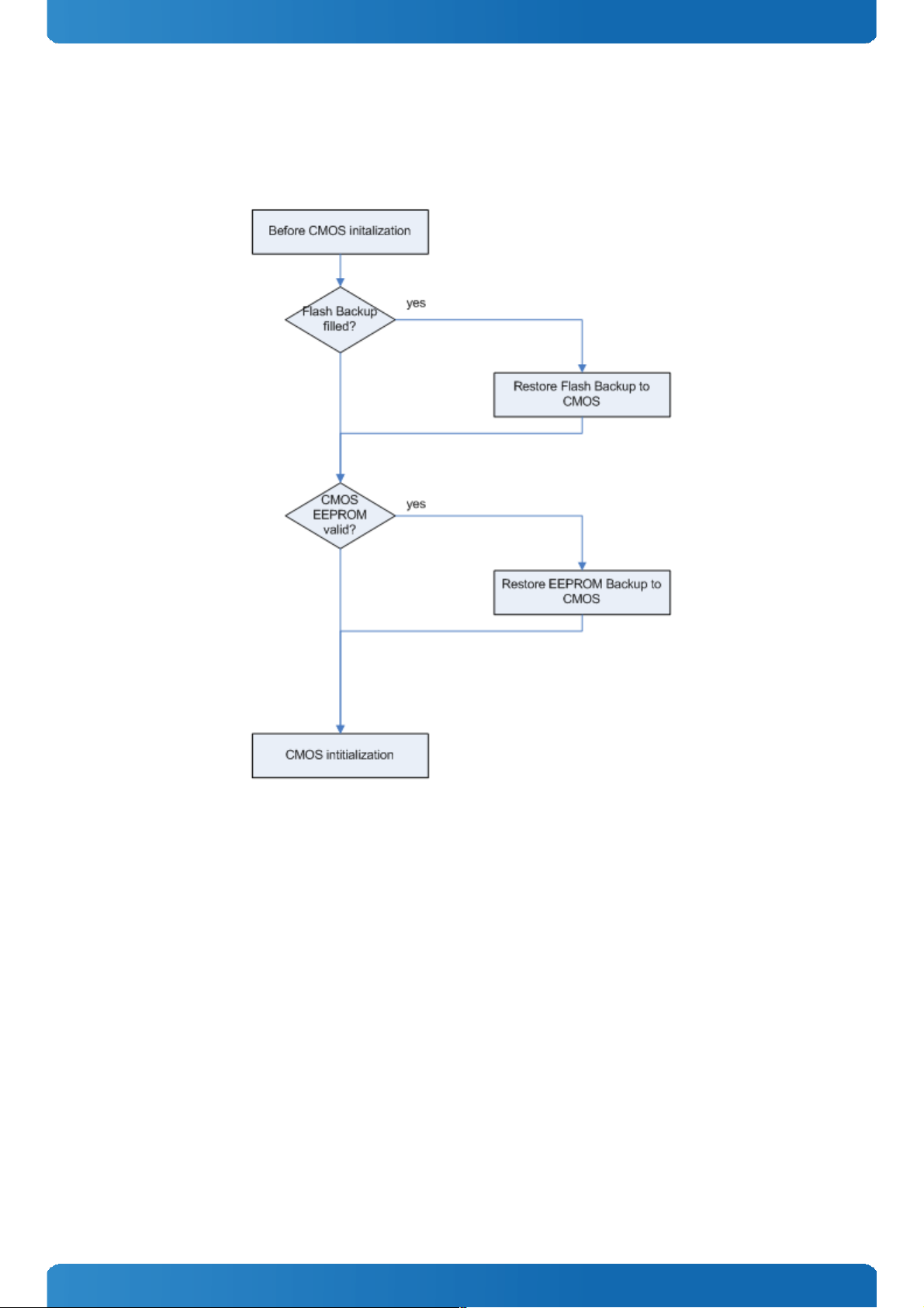
3.11 Flash Backup Feature
The COMe-cPC2 supports a new functionality called “Flash Backup”. This new feature allows saving custom defaults
directly into the Flash. With invalid EEPROM data or without a CMOS EEPROM, the module will start up with these custom
defaults. It’s possible to save this BIOS with changed defaults to an image and flash it on other modules.
37
Page 38

COMe-cPC2 / Features and Interfaces
To create a BIOS with custom defaults:
» Change your BIOS settings
» Save as custom defaults to RTC/Flash and Exit (module will now always start with these settings)
Flash Backup should show “Enter new Password” first time saving custom defaults. If it is
not possible to set a new password or entering a password shows an error message, please
clean up CMOS data with DOS command: jidacmos rtc /clean (jidacmos utility is available
at Kontron’s Customer Section)
» Extract the BIOS including custom defaults with afudos or kflash utility for windows
Tool Command
AFUDOS
c:\>afudos.exe biosname.rom /O
KFLASH
c:\>kflash.exe backup biosname.rom
Flash your BIOS with custom defaults:
To flash a BIOS with customized defaults extracted like described above, use following options
Operating System Command
Windows OS
c:\>kflash.exe flash biosname.rom /bncr
DOS
c:\>afudos.exe biosname.rom /p /b /n /c
c:\>jidacmos.exe eep /clean
kflash.exe is a shell tool included in Kontron K-Station System Utility Package.
jidacmos utility is included in the BIOS download packages at Kontron's customer section.
38
Page 39

COMe-cPC2 / Features and Interfaces
3.12 Speedstep Technology
The Intel® processors offers the Intel® Enhanced SpeedStep™ technology that automatically switches between maximum
performance mode and battery-optimized mode, depending on the needs of the application being run. It let you
customize high performance computing on your applications. When powered by a battery or running in idle mode, the
processor drops to lower frequencies (by changing the CPU ratios) and voltage, conserving battery life while maintaining
a high level of performance. The frequency is set back automatically to the high frequency, allowing you to customize
performance.
In order to use the Intel® Enhanced SpeedStep™ technology the operating system must support SpeedStep™ technology.
By disabling the SpeedStep feature in the BIOS, manual control/modification of CPU performance is possible. Setup the
CPU Performance State in the BIOS Setup or use 3rd party software to control CPU Performance States.
39
Page 40

COMe-cPC2 / Features and Interfaces
3.13 C-States
New generation platforms include power saving features like SuperLFM, EIST (P-States) or C-States in O/S idle mode.
Activated C-States are able to dramatically decrease power consumption in idle mode by reducing the Core Voltage or
switching of parts of the CPU Core, the Core Clocks or the CPU Cache.
Following C-States are defined:
CState
Description Function
C0 Operating CPU fully turned on
C1 Halt State Stops CPU main internal clocks via sof tware
C1E Enhanced Halt Similar to C1, additionally reduces CPU voltage
C2 Stop Grant Stops CPU internal and external clocks via hardware
C2E Extended Stop Grant Similar to C2, additionally reduces CPU voltage
C3 Deep Sleep Stops all CPU internal and external clocks
C3E Extended Stop Grant Similar to C3, additionally reduces CPU voltage
C4 Deeper Sleep Reduces CPU voltage
C4E Enhanced Deeper Sleep Reduces CPU voltage even more and turns off the memory cache
C6 Deep Power Down Reduces the CPU internal voltage to any value, including 0V
C7 Deep Power Down Similar to C6, additionally LLC (LastLevelCache) is switched off
C-States are usually enabled by default for low power consumption, but active C-States my influence performance
sensitive applications or real-time systems.
» Active C6-State may influence data transfer on external Serial Ports
» Active C7-State may cause lower CPU and Graphics performance
It's recommended to disable C-States / Enhanced C-States in BIOS Setup if any problems occur.
40
Page 41

COMe-cPC2 / Features and Interfaces
3.14 Dynamic FSB Frequency Switching
Dynamic FSB frequency switching effectively reduces the internal bus clock frequency in half to further decrease the
minimum processor operating frequency from the Enhanced Intel SpeedStep Technology performance states and achieve
the Super Low Frequency Mode (Super LFM). This feature is supported at FSB frequencies of 1066 MHz, 800 MHz and 667
MHz and does not entail a change in the external bus signal (BCLK) frequency. Instead, both the processor and GMCH
internally lower their BCLK reference frequency to 50% of the externally visible frequency. Both the processor and GMCH
maintain a virtual BCLK signal (VBCLK) that is aligned to the external BCLK but at half the frequency.
After a downward shift, it would appear externally as if the bus is running with a 133-MHz base clock in all aspects, except
that the actual external BCLK remains at 266 MHz. See Figure 3 for details. The transition into Super LFM, a “down-shift,”
is done following a handshake between the processor and GMCH. A similar handshake is used to indicate an “up-shift,” a
change back to normal operating mode. Please ensure this feature is enabled and supported in the BIOS.
41
Page 42

COMe-cPC2 / Features and Interfaces
3.15 VID-x
The processor implements the VID-x feature for improved control of core voltage levels when the processor enters a
reduced power consumption state. VID-x applies only when the processor is in the Intel Dynamic Acceleration Technology
performance state and one or more cores are in low-power state (i.e., CC3/CC4/CC6). VID-x provides the ability for the
processor to request core voltage level reductions greater than one VID tick. The amount of VID tick reduction is fixed and
only occurs while the processor is in Intel Dynamic Acceleration Technology mode. This improved voltage regulator
efficiency during periods of reduced power consumption allows for leakage current reduction which results in platform
power savings and extended battery life.
When in Intel Dynamic Acceleration Technology mode, it is possible for both cores to be active under certain internal
conditions. In such a scenario the processor may draw a Instantaneous current (ICC_CORE_INST) for a short duration of
tINST; however, the average ICC current will be lesser than or equal to ICCDES current specification.
42
Page 43

COMe-cPC2 / Features and Interfaces
3.16 Enhanced Intel Dynamic Acceleration Technology
The processor supports Intel Dynamic Acceleration Technology mode. The Intel Dynamic Acceleration Technology feature
allows one core of the processor to operate at a higher frequency point when the other core is inactive and the operating
system requests increased performance. This higher frequency is called the opportunistic frequency and the maximum
rated operating frequency is the ensured frequency. The processor includes a hysteresis mechanism that improves overall
Intel Dynamic Acceleration Technology performance by decreasing unnecessary transitions of the cores in and out of Intel
Dynamic Acceleration Technology mode. Normally, the processor would exit Intel Dynamic Acceleration Technology as
soon as two cores are active. This can become an issue if the idle core is frequently awakened for a short periods (i.e., high
timer tick rates). The hysteresis mechanism allows two cores to be active for a limited time before it transitions out of
Intel Dynamic Acceleration Technology mode.
Intel Dynamic Acceleration Technology mode enabling requires:
» Exposure, via BIOS, of the opportunistic frequency as the highest ACPI P state
» Enhanced Multi-Threaded Thermal Management (EMTTM)
» Intel Dynamic Acceleration Technology mode and EMTTM MSR configuration via BIOS
43
Page 44

COMe-cPC2 / Features and Interfaces
3.17 Usage of Different Graphic Interfaces
The COMe-cPC2 offers VGA, PCIexpress Graphics, LVDS, HDMI, SDVO and Displayport interfaces to connect graphical user
interfaces. The usage of VGA, PCIexpress and SDVO complies with the current COM Express® Specification.
The principle of using them is shown in the next drawing.
VGA and LVDS interface is always available and can be used. The pins of PCIexpress Graphics either are used as PCIexpress
Graphics or as HDMI/SDVO/DP, which is controlled by switch1.
Switch1 is the SDVO_SDA# line (C73). When this signal is high (2.5V) the SDVO/HDMI/DP output is enabled. Otherwise the
lines can be used as PCIexpressGraphic.
The switch 2 to select HDMI, SDVO or Displayport consists of the devices detected on the regarding sense circuits. When
there is an SDVO 2 TV/LVDS/DVI converter found on the SDVO_DATA and _CLK lines (C73; D73) then the output is switched
to SDVO. When there is Displayport device found on the Displayport AUX lines (C71; C72) then it is Display port and in any
other case the output is switched to HDMI.
44
Page 45

COMe-cPC2 / Features and Interfaces
3.18 Alternative Pin-out of HDMI
Pin Nr. Pin Name PCIexpress Pin Name HDMI HDMI Pin Description
D61 PCIexpress Graphics Transmit + 3 TMDS_B_CLK HDMI Port B Clock
D62 PCIexpress Graphics Transmit - 3 TMDS_B_CLK# HDMI port B Clock complement
D58 PCIexpress Graphics Transmit + 2 TMDS_B_DATA0 HDMI port B Data0
D59 PCIexpress Graphics Transmit - 2 TMDS_B_DATA0# HDMI por t B Data0 complement
D55 PCIexpress Graphics Transmit + 1 TMDS_B_DATA1 HDMI port B Data1
D56 PCIexpress Graphics Transmit - 1 TMDS_B_DATA1# HDMI por t B Data1 complement
D52 PCIexpress Graphics Transmit + 0 TMDS_B_DATA2 HDMI port B Data2
D53 PCIexpress Graphics Transmit - 0 TMDS_B_DATA2# HDMI por t B Data2 complement
C61 PCIexpress Graphics Receive + 3 TMDS_B_HPD# HDMI port B Hot-plug detect
D74 PCIexpress Graphics Transmit + 7 TMDS_C_CLK HDMI port C Clock
D75 PCIexpress Graphics Transmit – 7 TMDS_C_CLK# HDMI por t C Clock complement
D71 PCIexpress Graphics Transmit + 6 TMDS_C_DATA0 HDMI por t C Data0
D72 PCIexpress Graphics Transmit – 6 TMDS_C_DATA0# HDMI port C Data0 complement
D68 PCIexpress Graphics Transmit + 5 TMDS_C_DATA1 HDMI por t C Data1
D69 PCIexpress Graphics Transmit – 5 TMDS_C_DATA1# HDMI port C Data1 complement
D65 PCIexpress Graphics Transmit + 4 TMDS_C_DATA2 HDMI por t C Data2
D66 PCIexpress Graphics Transmit – 4 TMDS_C_DATA2# HDMI port C Data2 complement
C74 PCIexpress Graphics Receive + 7 TMDS_C_HDP# HDMI port C Hot-plug detect
3.19 Alternative Pin-out of Display Port
Pin Nr. Pin Name PCIexpress Pin Name HDMI HDMI Pin Description
D61 PCIexpress Graphics Transmit + 3 DPB_LANE3 Displayport B Lane3
D62 PCIexpress Graphics Transmit – 3 DPB_LANE3# Displayport B Lane3 complement
D58 PCIexpress Graphics Transmit + 2 DPB_LANE2 Displayport B Lane2
D59 PCIexpress Graphics Transmit – 2 DPB_LANE2# Displayport B Lane2 complement
D55 PCIexpress Graphics Transmit + 1 DPB_LANE1 Displayport B Lane1
D56 PCIexpress Graphics Transmit - 1 DPB_LANE1# Displayport B Lane1 complement
D52 PCIexpress Graphics Transmit + 0 DPB_LANE0 Displayport B Lane0
D53 PCIexpress Graphics Transmit – 0 DPB_LANE0# Displayport B Lane0 complement
C61 PCIexpress Graphics Receive + 3 DPB_HPD# Displayport B Hot-plug detect
C58 PCIexpress Graphics Receive + 2 DPB_AUX Displayport B Aux
C59 PCIexpress Graphics Receive – 2 DPB_AUX# Displayport B Aux complement
D74 PCIexpress Graphics Transmit + 7 DPC_LANE3 Displaypor t C Lane3
D75 PCIexpress Graphics Transmit – 7 DPC_LANE3# Displaypor t C Lane3 complement
D71 PCIexpress Graphics Transmit + 6 DPC_LANE2 Displaypor t C Lane2
D72 PCIexpress Graphics Transmit – 6 DPC_LANE2# Displaypor t C Lane2 complement
D68 PCIexpress Graphics Transmit + 5 DPC_LANE1 Displaypor t C Lane1
D69 PCIexpress Graphics Transmit – 5 DPC_LANE1# Displaypor t C Lane1 complement
D65 PCIexpress Graphics Transmit + 4 DPC_LANE0 Displaypor t C Lane0
D66 PCIexpress Graphics Transmit – 4 DPC_LANE0# Displaypor t C Lane0 complement
C74 PCIexpress Graphics Receive + 7 DPC_HPD# Displayport C Hot-plug detect
C71 PCIexpress Graphics Receive + 6 DPC_AUX Displayport C Aux
C72 PCIexpress Graphics Receive – 6 DPC_AUX# Displayport C Aus complement
D88 PCIexpress Graphics Transmit + 11 DPD_LANE3 Displaypor t D Lane3
D89 PCIexpress Graphics Transmit – 11 DPD_LANE3# Displaypor t D Lane3 complement
D85 PCIexpress Graphics Transmit + 10 DPD_LANE2 Displaypor t D Lane2
D86 PCIexpress Graphics Transmit – 10 DPD_LANE2# Displaypor t D Lane2 complement
D81 PCIexpress Graphics Transmit + 9 DPD_LANE1 Displayport D Lane1
D82 PCIexpress Graphics Transmit – 9 DPD_LANE1# Displayport D Lane1 complement
D78 PCIexpress Graphics Transmit + 8 DPD_LANE0 Displayport D Lane0
D77 PCIexpress Graphics Transmit – 8 DPD_LANE0# Displayport D Lane0 complement
C88 PCIexpress Graphics Receive + 11 DPD_HPD# Displayport D Hot-plug detect
C85 PCIexpress Graphics Receive + 10 DPD_AUX Displayport D Aux
C86 PCIexpress Graphics Receive – 10 DPD_AUX# Displayport D Aus complement
45
Page 46

COMe-cPC2 / Features and Interfaces
3.20 Display Configurations
The chapter describes possible display configurations and supported features for the integrated Intel® GMA X4500MHD
(Gen5.5) graphics.
Display N/A CRT LVDS fixed LVDS DID LVDS2DVI DP DP2DVI DP2HDMI DP2CRT
N/A
- S S S S S S S S
CRT
S - A A A A A A A
LVDS fixed
S A - - - A A A A
LVDS DID
S A - - - A A A A
LVDS2DVI
S A - - - A A A A
DP
S A A A A A A A A
DP2DVI
S A A A A A A A A
DP2HDMI
S A A A A A A A A
DP2CRT
S A A A A A A A tbd
» S = Single Display
» A = All Modes (Single Display, Clone Mode, Extended Desktop)
» - = Not supported
» N/A = Display not attached
Tested in Windows 7 with Intel GMA HD 15.15.6.1892, BIOS CNTGR414
46
Page 47

COMe-cPC2 / Features and Interfaces
Digital Display Interface Features
The integrated Intel® GMA X4500MHD (Gen5.5) graphics supports:
» One stream high-bandwidth Digital Content Protection (HDCP) on HDMI or DisplayPort (requires optional available
HDCP Key)
» One active Protected Audio and Video Path (PAVP) session on HDMI or DisplayPort
» HDMI Audio if activated in BIOS and O/S
» DP/HDMI/DVI Hot-plug (low-active)
DDI Design Consideration
» For sufficient signal quality baseboard designs with long signal lanes or impedance leaps may require an Equalicer
or Redriver for the digital display interfaces
» Monitor Hot-plug detection is usually high-active. On COMe-cPC2 the hot-plug is low active and requires conversion
on the baseboard
Supported Audio Formats on HDMI
» AC-3 Dolby Digital
» Dolby Digital Plus
» DTS-HD
» LPCM, 192kHz/24bit, 8 channel
» Dolby True HD, DTS HD Master Audio
47
Page 48

COMe-cPC2 / Features and Interfaces
3.21 Hybrid Graphics / Multi-monitor
The COMe-cPC2 supports Hybrid Multi-monitor function which is one form of Intel's Hybrid Graphics where integrated
graphics (in Chipset or CPU) is available to operate simultaneously with external PEG; PCIe or PCI graphics. This feature
enables concurrent function of Intel's integrated Graphics Processing Unit (GPU/iGFX) along with a discrete GPU solution,
allowing for operability of greater than two independently-driven displays. The O/S will handle control of the multiple
GPU display adapters appropriately. For example, WindowsXP supports The Microsoft Windows XP Display Driver Model
(XPDM) which allows loading and support of multiple graphics drivers. Windows 7 continues that legacy XPDM support but
also adds WDDM v1.1 which, like XPDM, allows for simultaneous multiple graphics drivers (Windows Vista WDDM v1.0 did
not allow this capability). Operating system applications will be adapter-unaware through use of the O/S GUI APIs and will
utilize the adapter associated with the primary display, regardless of which display the image is located on.
Some applications may be adapter-aware, e.g., full-screen applications and system
applications like the compositor. A number of software tools designed to assist multimonitor use are available from third parties. One example is the UltraMon* utility for multimonitor systems, which helps with the position of applications, assists desktop wallpapers
and screen savers in multi-monitor configurations.
Hybrid Multi-monitor mode is recommended to be accomplished using a discrete third-party PCI Express graphics card
either into the PEG slot of the platform or into an available PCI Express slot routed off of the I/O subsection of the chipset.
Requirements
» Baseboard supporting PEG (alternatively PCIe or PCI)
» Module BIOS which allows switching between iGFX and discrete GPU (iGFX must be set to primary boot display)
» O/S supporting heterogeneous display adapters (Linux / WindowsXP / Windows 7)
Setup a Multi-monitor system
» Start without the discrete GPU seated in the system
» Select IGD as Primary Boot Display in BIOS Setup
» Boot into O/S and install drivers requested for the integrated GPU
» Shut down the system and insert the discrete GPU
» Boot into O/S and install drivers requested for the discrete GPU (if necessary in Safe mode)
» Set the Windows Display properties as referenced below (example: WindowsXP)
48
Page 49

COMe-cPC2 / Features and Interfaces
In most cases the graphical user interfaces (e.g. ATI Catalyst Control Center) for both GPUs
may not run properly. It's recommended to use O/S implemented Display Properties like in
screenshot above
Detailed documentation is available in Intel Paper 323214
49
Page 50

COMe-cPC2 / Features and Interfaces
3.22 Intel® vPro™ technology
Kontron and Intel® are addressing the security and manageability challenges facing embedded systems today with the
implementation of Intel® vPro™ technology to enable: » System integrity » Secure isolation » Remote systems
management
First, system integrity is the ability to identify whether the system hardware or system software has been modified
without authorization. When a system’s integrity is known, the system can be thought of as a trusted system. Second,
secure isolation is the ability to use platform hardware to separate processes, resources, and data on the system such that
they cannot interact with each other in unintended ways. By providing hardware-assisted isolation, there are limitless
security, privacy, and cost savings that can be realized through consolidation and workload isolation. Finally, remote
systems management is the ability to troubleshoot, perform power management or system verification through secure
channels. Significant cost savings and efficiencies can be realized through remote management allowing for increased
system up time and the ability to manage or diagnose a system, even when powered down.
Intel® vPro™ technology itself is special functionality designed into the both the processor and the chipset. The three
technologies that comprise Intel® vPro™ technology are: Intel Virtualization Technology (Intel® VT), Intel Trusted
Execution Technology (Intel® TXT) and Intel Active Management Technology (Intel® AMT).
Intel® VT provides hardware-based assists making secure isolation more efficient and decreases the virtualization
footprint, lowering the effective attack surface of a solution. This hardware-based technology can help to protect
applications and information by running multiple operating systems (OSs) in isolation on the same physical system. A
virtual guest OS can be created in an entirely separate space on the physical system to run specialized or critical
applications. Virtual environments leverage Intel® VT for memory, CPU, and Directed I/O virtualization. Intel® TXT
provides the ability to use hardware-based mechanisms to verify system integrity during the boot process. It also provides
system memory scrubbing that protects against soft reset attacks. Virtualized environments take advantage of Intel® TXT
launch environment verification to establish a dynamic root of trust providing added security to hypervisor or virtual
machine monitor (VMM).
Mechanisms employed by Intel® AMT include domain authentication, session keys, persistent data storage in the Intel®
AMT hardware, and access control lists. Only firmware images that are digitally signed by Intel are permitted to load and
execute. This set of hardware-based features is targeted for businesses and allows remote access to the system, whether
wired or wireless, for management and security tasks. Because of the special hardware capabilities provided by Intel®
AMT, out of band access is available even when the OS is not functional or system power is off.
Intel® TXT and Intel® AMT are disabled by default. Please contact your local sales or
support for BIOS versions with full vPro™ support
50
Page 51

COMe-cPC2 / Features and Interfaces
3.23 ACPI Suspend Modes and Resume Events
The COMe-cPC2 supports the S3 state (=Save to Ram). S4 (=Save to Disk) is not supported by the BIOS (S4_BIOS) but
S4_OS is supported by the following operating systems:
» Windows XP
» Windows Vista
» Windows 7
The following events resume the system from S3:
» USB Keyboard (1)
» USB Mouse (1)
» Power Button
» WakeOnLan (2)
The following events resume the system from S4:
» Power Button
» WakeOnLan (2)
The following events resume the system from S5:
» Power Button
» WakeOnLan (2)
(1) OS must support wake up via USB devices and baseboard must power the USB Port with
StBy-Voltage
(2) WakeOnLan must be enabled in BIOS setup and driver options
51
Page 52

COMe-cPC2 / System Resources
4 System Resources
4.1 Interrupt Request (IRQ) Lines
Please be aware that an ACPI OS decides itself on resource usage. The tables below show only an example distribution.
4.1.1 In 8259 PIC Mode
IRQ# Used For Available Comment
0 Timer 0 No -
1 Keyboard No Note (4)
2 Slave 8259 No -
3 - Yes -
4 - Yes -
5 - Yes -
6 - Yes -
7 - Yes -
8 RTC No -
9 SCI No Note (3)
10 - Yes -
11 - Yes -
12 PS/2 Mouse No Note (5)
13 FPU No -
14 IDE0 No Note (1)(2)
15 IDE1 No Note (1)(2)
1 If the “Used For” device is disabled in setup, the corresponding interrupt is available for
other devices.
2 if sata controller is operating in legacy mode
3 Unavailable in Advanced Configuration and Power Interface (ACPI) mode. Used as System
Control Interrupt (SCI) in ACPI mode. Currently not free in Non-ACPI mode.
4 used by legacy keyboard controller when available on carrier board.
5 used by legacy ps/2 mouse controller when available on carrier board.
52
Page 53

COMe-cPC2 / System Resources
4.1.2 In APIC mode
IRQ# Used For Available Comment
0 T imer 0 No -
1 Keyboard No -
2 Slave 8259 No -
3 - Yes Note (4)
4 - Yes Note (4)
5 - Yes Note (4)
6 - Yes Note (4)
7 - Yes Note (4)
8 RTC No -
9 SCI No Note (2)
10 - Yes Note (4)
11 - Yes Note (4)
12 - Yes Note (4)
13 FPU No -
14 IDE0 No Note (1)(3)
15 IDE1 No Note (1)(3)
16 PIRQ[A] For PCI PCI IRQ line 1 + Graphics controller + HD Audio Controller + secondary IDE Note (4)
17 PIRQ[B] For PCI PCI IRQ line 2 + HD Audio controller Note (4)
18 PIRQ[C] For PCI PCI IRQ line 3 + USB UCHI controller #3 + SATA (native mode) Note (4)
19 PIRQ[D] For PCI PCI IRQ line 4 + USB UCHI controller #2 + IDE (native mode) Note (4)
20 PIRQ[E] No Lan Controller Note (4)
21 PIRQ[F] No Note (4)
22 PIRQ[G] No Note (4)
23 PIRQ[H] No USB EHCI controller, USB UCHI controller #1 Note (4)
1 If the “Used For” device is disabled in setup, the corresponding interrupt is available for
other devices.
2 Unavailable in Advanced Configuration and Power Interface (ACPI) mode. Used as System
Control Interrupt (SCI) in ACPI mode. Currently not free in Non-ACPI mode.
3 IRQs are available if IDE controller is either disabled in setup or if in Native IDE mode.
4 ACPI Operating System decides on particular IRQ usage.
4.2 Direct Memory Access (DMA) Channels
DMA# Used For Available Comment
0 - No -
1 - No -
2 - No -
3 - No -
4 Cascade No -
5 - No -
6 - No -
7 - No -
4.3 Memory Area
Upper Memory Used For Available Comment
C0000h-CFFFFh VGA BIOS No -
D0000h-DFFFFh - Yes LPC Bus or Shadow RAM
E0000h-EFFFFh System BIOS No -
53
Page 54

COMe-cPC2 / System Resources
4.4 I/O Address Map
Upper Memory Used For Available Comment
400h-41Fh Chipset No Always used by chipset
4D0h-4D1h Interrupt Controller No -
500h-53Fh Chipset No Always used by chipset
800h-87Fh Chipset No Always used by chipset
1000h> PCI No -
4.5 External Inter-IC (I2C) Bus
I2C Address Used For Available Comment JIDA Bus Nr.
- - - - 2
4.6 System Management (SM) Bus
SMB Address Used For Available Comment JIDA Bus Nr.
10h SMB Host No EEPROM for CMOS Data 1
12h SMART_Charger No Only be used by a SMB Charger 1
14h SMART_Selector No Only be used by a SMB Selector
or Manager
1
16h SMART_Battery No Only be used by a SMB Battery 1
A0h SPD No DDR3 channel A 1
A4h SPD No DDR3 channel B 1
5Ch HW-Monitor No - 1
D2h Clockgenerator No - 1
4.7 JILI I2C Bus
I2C Address Used For Available Comment JIDA Bus Nr.
A0h DDC No Display Data 6
62h MAX6253 No DAC for Backlight brightness 6
4.8 SDVO I2C Bus
I2C Address Used For Available Comment JIDA Bus Nr.
A0h DDC No Display Data 4
4.9 CRT I2C Bus
I2C Address Used For Available Comment JIDA Bus Nr.
A0h DDC No Display Data 5
JIDA Bus Nr. 0 and Bus Nr. 3 are for internal use only.
54
Page 55

COMe-cPC2 / Connectors
5 Connectors
The pinouts for Interface Connectors X1A and X1B are documented for convenient reference. Please see the COM Express®
Specification and COM Express® Design Guide for detailed, design-level information.
5.1 Connector Location
55
Page 56

COMe-cPC2 / Connectors
5.2 Pinout List
5.2.1 General Signal Description
Type Descr iption
I/O-3,3
Bi-directional 3,3 V IO-Signal
I/O-5T
Bi-dir. 3,3V I/O (5V Tolerance)
I/O-5
Bi-directional 5V I/O-Signal
I-3,3
3,3V Input
I/OD
Bi-directional Input/Output Open Drain
I-5T
3,3V Input (5V Tolerance)
OA
Output Analog
OD
Output Open Drain
O-1,8
1,8V Output
O-3,3
3,3V Output
O-5
5V Output
DP-I/O
Differential Pair Input/Output
DP-I
Differential Pair Input
DP-O
Differential Pair Output
PU
Pull-Up Resistor
PD
Pull-Down Resistor
PWR
Power Connection
To protect external power lines of peripheral devices, make sure that: the wires have the
right diameter to withstand the maximum available current the enclosure of the peripheral
device fulfills the fire-protection requirements of IEC/EN60950
56
Page 57

COMe-cPC2 / Connectors
5.2.2 Connector X1A Row A
Pin Signal Description Type Termination Comment
A1 GND Power Ground PWR - -
A2 GBE0_MDI3- GBE0_MDI3_N ; Ethernet Receive Data - DP-I - -
A3 GBE0_MDI3+ GBE0_MDI3_P ; Ethernet Receive Data - DP-I - -
A4 GBE0_LINK100# GBE0_LINK100# ; Ethernet Speed LED O-3,3 - -
A5 GBE0_LINK1000# GBE0_LINK1000# ; Ethernet Speed LED O-3,3 - -
A6 GBE0_MDI2- GBE0_MDI2_N ; Ethernet Receive Data - DP-I - -
A7 GBE0_MDI2+ GBE0_MDI2_P ; Ethernet Receive Data - DP-I - -
A8 GBE0_LINK# GBE0_LINK# ; LAN Link LED OD - -
A9 GBE0_MDI1- GBE0_MDI1_N ; Ethernet Receive Data - DP-I - -
A10 GBE0_MDI1+ GBE0_MDI1_P ; Ethernet Receive Data + DP-I - -
A11 GND Power Ground PWR - -
A12 GBE0_MDI0- GBE0_MDI0_N ; Ethernet Transmit Data - DP-O - -
A13 GBE0_MDI0+ GBE0_MDI0_P ; Ethernet Transmit Data + DP-O - -
A14 GBE0_CTREF GBE0_CTREF O-1,8 - is on a power rail controlled by Intels ME
A15 SUS_S3# PM_SLP_S3_EXT# O-3,3 PU 10k 3,3V (S5) -
A16 SATA0_TX+ SATA_TX0_P ; SATA 0 Transmit Data + Nc - -
A17 SATA0_TX- SATA_TX0_N ; SATA 0 Transmit Data - Nc - -
A18 SUS_S4# PM_SLP_S4_EXT# O-3,3 - -
A19 SATA0_RX+ SATA_RX0_P ; SATA 0 Receive Data + Nc - -
A20 SATA0_RX- SATA_RX0_N ; SATA 0 Receive Data - Nc - -
A21 GND Power Ground PWR - -
A22 SATA2_TX+ SATA_TX2_P ; SATA 2 Transmit Data + DP-O - -
A23 SATA2_TX- SATA_TX2_N ; SATA 2 Transmit Data - DP-O - -
A24 SUS_S5# PM_SLP_S#5 O-3,3 - -
A25 SATA2_RX+ SATA_RX2_P ; SATA 2 Receive Data + DP-I - -
A26 SATA2_RX- SATA_RX2_N ; SATA 2 Receive Data - DP-I - -
A27 BATLOW# PM_BATLOW# ; Battery Low I-3,3 PU 8k25 3,3V (S5) -
A28 ATA_ACT# ATA_LED# ; SATA LED O-3,3 PU 10k 3,3V (S0) int. PU 15k in ICH9 only active if
PLTRST#=0
A29 AC_SYNC HDA_SYNC ; HD Audio Sync O-3,3 - opt. for x4: PU 1k 3,3V(S0)
A30 AC_RST# HDA_RST# ; HD Audio Reset O-3,3 - int. PD 20k in ICH9
A31 GND Power Ground PWR - -
A32 AC_BITCLK HDA_BITCLK ; HD Audio Clock O-3,3 - int. PD 20k in ICH9 active only in S3
A33 AC_SDOUT HDA_SDOUT ; HD Audio Data O-3,3 - int. PD 20k in ICH9– x4 PU 1k 3,3V(S0) ⇒
A34 BIOS_DISABLE# BIOS_DISABLE# I-3,3 - -
A35 THRMTRIP# EXT_THRMTRIP# I/O-3,3 PU 10k 3,3V (S0) -
A36 USB6- USB6_N ; USB Data – Port6 DP-I/O - int. PD 15k in ICH9 ; 5V tolerant
A37 USB6+ USB6_P ; USB Data + Port6 DP-I/O - int. PD 15k in ICH9 ; 5V tolerant
A38 USB_6_7_OC# USB_67_OC# ; USB OverCurrent Port 6/7 I-3,3 PU 10k 3,3V (S5) -
A39 USB4- USB4_N ; USB Data - Port4 DP-I/O - int. PD 15k in ICH9 ; 5V tolerant
A40 USB4+ USB4_P ; USB Data + Port4 DP-I/O - int. PD 15k in ICH9 ; 5V tolerant
A41 GND Power Ground PWR - -
A42 USB2- USB2_N ; USB Data - Port2 DP-I/O - int. PD 15k in ICH9 ; 5V tolerant
A43 USB2+ USB2_P ; USB Data + Port2 DP-I/O - int. PD 15k in ICH9 ; 5V tolerant
A44 USB_2_3_OC# USB_23_OC# ; USB OverCurrent Port 2/3 I-3,3 PU 10k 3,3V (S5) -
A45 USB0- USB0_N ; USB Data - Port0 DP-I/O - int. PD 15k in ICH9 ; 5V tolerant
A46 USB0+ USB0_P ; USB Data + Port0 DP-I/O - int. PD 15k in ICH9 ; 5V tolerant
A47 VCC_RTC V_BAT PWR 3V - -
A48 EXCD0_PERST# EXCD0_PERST#;Express card reset O-3,3 - -
A49 EXCD0_CPPE# EXCD0_CPPE# ; capable c. request I-3,3 PU 10k 3,3V (S5) -
A50 LPC_SERIRQ LPC_SERIRQ ; Serial Interrupt Request IO-3,3 PU 10k 3,3V (S0) -
A51 GND Power Ground PWR - -
A52 PCIE_TX5+ opt. PCI Express lane 5 + Transmit Nc - just available if no GbEthernet PHY is used.
A53 PCIE_TX5- opt. PCI Express lane 5 - Transmit Nc - just available if no GbEthernet PHY is used.
A54 GPI0 EXT_GPI0 ; General Purpose Input 0 I-3,3 PU 10k 3,3V (S0) -
A55 PCIE_TX4+ PCI Express lane 4 + Transmit DP-O - -
A56 PCIE_TX4- PCI Express lane 4 - Transmit DP-O - -
A57 GND Power Ground PWR - -
A58 PCIE_TX3+ PCI Express lane 3 + Transmit DP-O - -
A59 PCIE_TX3- PCI Express lane 3 - Transmit DP-O - -
A60 GND Power Ground PWR - -
A61 PCIE_TX2+ PCI Express lane 2 + Transmit DP-O - -
A62 PCIE_TX2- PCI Express lane 2 - Transmit DP-O - -
A63 GPI1 EXT_GPI1 ; General Purpose Input 1 I-3,3 PU 10k 3,3V (S0) -
57
Page 58

COMe-cPC2 / Connectors
A64 PCIE_TX1+ PCI Express lane 1 + Transmit DP-O - -
A65 PCIE_TX1- PCI Express lane 1 - Transmit DP-O - -
A66 GND Power Ground PWR - -
A67 GPI2 EXT_GPI2 ; General Purpose Input 2 I-3,3 PU 10k 3,3V (S0) -
A68 PCIE_TX0+ PCI Express lane 0 + Transmit DP-O - -
A69 PCIE_TX0- PCI Express lane 0 - Transmit DP-O - -
A70 GND Power Ground PWR - -
A71 LVDS_A0+ LVDS_A_DATA0_P ; LVDS Channel A Data0+ DP-O - -
A72 LVDS_A0- LVDS_A_DATA0_N ; LVDS Channel A Data0- DP-O - -
A73 LVDS_A1+ LVDS_A_DATA1_P ; LVDS Channel A Data1+ DP-O - -
A74 LVDS_A1- LVDS_A_DATA1_N ; LVDS Channel A Data1- DP-O - -
A75 LVDS_A2+ LVDS_A_DATA2_P ; LVDS Channel A Data2+ DP-O - -
A76 LVDS_A2- LVDS_A_DATA2_N ; LVDS Channel A Data2- DP-O - -
A77 LVDS_VDD_EN LVDS_VDD_EN ; LVDS Panel Power Control O-3,3 PD 100k -
A78 LVDS_A3+ LVDS_A_DATA3_P ; LVDS Channel A Data3+ DP-O - -
A79 LVDS_A3- LVDS_A_DATA3_N ; LVDS Channel A Data3- DP-O - -
A80 GND Power Ground PWR - -
A81 LVDS_A_CK+ LVDS_A_CLK_P ; LVDS Channel A Clock+ DP-O - -
A82 LVDS_A_CK- LVDS_A_CLK_N ; LVDS Channel A Clock- DP-O - -
A83 LVDS_I2C_CK LVDS_DDC_CLK ; JILI I2C Clock I/O-3,3 PU 2k21 3,3V (s0) -
A84 LVDS_I2C_DAT LVDS_DDC_DATA ; JILI I2C Data I/O-3,3 PU 2k21 3,3V (s0) -
A85 GPI3 EXT_GPI3 ; General Purpose Input 3 I-3,3 PU 10k 3,3V (S0) -
A86 KBD_RST# KBD_RST# ; Keyboard Reset I-3,3 PU 10k 3,3V (S0) -
A87 KBD_A20GATE KBD_A20GATE I-3,3 PU 10k 3,3V (S0) -
A88 PCIE0_CK_REF+ CLK_PCIE_CON_P DP-O - -
A89 PCIE0_CK_REF- CLK_PCIE_CON_N DP-O - -
A90 GND Power Ground PWR - -
A91 RSVD n.c. Nc - -
A92 RSVD n.c. Nc - -
A93 GPO0 EXT_GPO0 ; General Purpose Output 0 O-3,3 PD 10k -
A94 RSVD n.c. Nc - -
A95 RSVD n.c. Nc - -
A96 GND Power Ground PWR - -
A97 VCC_12V 12V VCC PWR - 8.5-18V
A98 VCC_12V 12V VCC PWR - 8.5-18V
A99 VCC_12V 12V VCC PWR - 8.5-18V
A100 GND Power Ground PWR - -
A101 VCC_12V 12V VCC PWR - 8.5-18V
A102 VCC_12V 12V VCC PWR - 8.5-18V
A103 VCC_12V 12V VCC PWR - 8.5-18V
A104 VCC_12V 12V VCC PWR - 8.5-18V
A105 VCC_12V 12V VCC PWR - 8.5-18V
A106 VCC_12V 12V VCC PWR - 8.5-18V
A107 VCC_12V 12V VCC PWR - 8.5-18V
A108 VCC_12V 12V VCC PWR - 8.5-18V
A109 VCC_12V 12V VCC PWR - 8.5-18V
A110 GND Power Ground PWR - -
58
Page 59

COMe-cPC2 / Connectors
5.2.3 Connector X1A Row B
Pin Signal Description Type Termination Comment
B1 GND Power Ground PWR - -
B2 GBE0_ACT GBE0_ACT# ; Ethernet Activity LED OD - -
B3 LPC_FRAME# LPC_FRAME# ; LPC Frame Indicator I-3,3 - -
B4 LPC_AD0 LPC_AD0 ; LPC Adress & DATA Bus I/O-3,3 - int. PU 20k in ICH9
B5 LPC_AD1 LPC_AD1 ; LPC Adress & DATA Bus I/O-3,3 - int. PU 20k in ICH9
B6 LPC_AD2 LPC_AD2 ; LPC Adress & DATA Bus I/O-3,3 - int. PU 20k in ICH9
B7 LPC_AD3 LPC_AD3 ; LPC Adress & DATA Bus I/O-3,3 - int. PU 20k in ICH9
B8 LPC_DRQ0# LPC_DRQ#0 ; LPC Request 0 I-3,3 PU 10k 3,3V (S0) int. PU 20k in ICH9
B9 LPC_DRQ1# LPC_DRQ#1 ; LPC Request 1 I-3,3 PU 10k 3,3V (S0) int. PU 20k in ICH10
B10 LPC_CLK CLK_LPC_33M_EXT ; 33MHz LPC clock O-3,3 - -
B11 GND Power Ground PWR - -
B12 PWRBTN# EXT_PWRBTN# ; Power Button I-3,3 PU 20k 3,3V (S5) -
B13 SMB_CK SMB_CLK_EXT ; SMBUS Clock O-3,3 PU 2k2 3,3V (S5) -
B14 SMB_DAT SMB_DATA_EXT ; SMBUS Data IO-3,3 PU 2k2 3,3V (S5) -
B15 SMB_ALERT# SMB_ALERT# ; SMBUS Interrupt IO-3,3 PU 1k0 3,3V (S5) -
B16 SATA1_TX+ SATA_TX1_P ; SATA 1 Transmit Data + DP-O - -
B17 SATA1_TX- SATA_TX1_N ; SATA 1 Transmit Data - DP-O - -
B18 SUS_STAT# PM_SUS_ STAT# O-3,3 - -
B19 SATA1_RX+ SATA_RX1_P ; SATA 1 Receive Data + DP-I - -
B20 SATA1_RX- SATA_RX1_N ; SATA 1 Receive Data - DP-I - -
B21 GND Power Ground PWR - -
B22 SATA3_TX+ opt. SATA_TX3_P ; SATA 3 Transmit Data + DP-O - -
B23 SATA3_TX- opt. SATA_TX3_N ; SATA 3 Transmit Data - DP-O - -
B24 PWR_OK EXT_PWR_OK ; Power OK I-3,3 - -
B25 SATA3_RX+ SATA_RX3_P ; SATA 3 Receive Data + DP-I - -
B26 SATA3_RX- SATA_RX3_N ; SATA 3 Receive Data - DP-I - -
B27 WDT WDT ; Watch Dog Timer O-3,3 - -
B28 AC_SDIN2 HDA_SDIN2_ICH ; HD Audio Serial Input Data 2 I-3,3 - int. PD 20k in ICH9
B29 AC_SDIN1 HDA_SDIN1_ICH ; HD Audio Serial Input Data 1 I-3,3 - int. PD 20k in ICH9
B30 AC_SDIN0 HDA_SDIN0_ICH ; HD Audio Serial Input Data 0 I-3,3 - int. PD 20k in ICH9
B31 GND Power Ground PWR - -
B32 SPKR HDA_SPKR ; Speaker O-3,3 - int. PD 20k in ICH9
B33 I2C_CK I2C_CLK_EXT ; I2C clock O-3,3 PU 2k21 3,3V (S0) -
B34 I2C_DAT I2C_DATA_EXT ; I2C data I/O-3,3 PU 2k21 3,3V (S0) -
B35 THRM# PM_THRM# ; Over Temperature O-3,3 PU 8k25 3,3V (S0) -
B36 USB7- USB7_N ; USB Data – Port7 DP-I/O - int. PD 15k in ICH9 ; 5V tolerant
B37 USB7+ USB7_P ; USB Data + Por t7 DP-I/O - int. PD 15k in ICH9 ; 5V tolerant
B38 USB_4_5_OC# USB_45_OC# ; USB OverCurrent Port 4/5 I-3,3 PU 10k 3,3V (S5) -
B39 USB5- USB5_N ; USB Data – Port5 DP-I/O - int. PD 15k in ICH9 ; 5V tolerant
B40 USB5+ USB5_P ; USB Data + Por t5 DP-I/O - int. PD 15k in ICH9 ; 5V tolerant
B41 GND Power Ground PWR - -
B42 USB3- USB3_N ; USB Data – Port3 DP-I/O - int. PD 15k in ICH9 ; 5V tolerant
B43 USB3+ USB3_P ; USB Data + Por t3 DP-I/O - int. PD 15k in ICH9 ; 5V tolerant
B44 USB_0_1_OC# USB_01_OC# ; USB OverCurrent Port 0/1 I-3,3 PU 10k 3,3V (S5) -
B45 USB1- USB1_N ; USB Data – Port1 DP-I/O - int. PD 15k in ICH9 ; 5V tolerant
B46 USB1+ USB1_P ; USB Data + Por t1 DP-I/O - int. PD 15k in ICH9 ; 5V tolerant
B47 EXCD1_PERST# EXCD1_PERST# ; Express card reset O-3,3 - -
B48 EXCD1_CPPE# EXCD1_CPPE# ; capable c. request I-3,3 PU 10k 3,3V (S5) -
B49 SYS_RESET# EXT_SYS_RESET# ; Reset Input I-3,3 PU 10k 3,3V (S5) -
B50 CB_RESET# CB_RESET# ; Carrier board Reset O-3,3 - -
B51 GND Power Ground PWR - -
B52 PCIE_RX5+ opt. PCI Express lane 5 + Recieve Nc - just available if no GbEthernet PHY is used.
B53 PCIE_RX5- opt. PCI Express lane 5 - Recieve Nc - just available if no GbEthernet PHY is used.
B54 GPO1 EXT_GPO1 ; General Purpose Output 1 O-3,3 PD 10k -
B55 PCIE_RX4+ PCI Express lane 4 + Recieve DP-I - availlable when ICH9-MDH or -R
B56 PCIE_RX4- PCI Express lane 4 - Recieve DP-I - availlable when ICH9-MDH or -R
B57 GPO2 EXT_GPO2 ; General Purpose Output 2 O-3,3 PD 10k -
B58 PCIE_RX3+ PCI Express lane 3 + Recieve DP-I - availlable when ICH9-MDH or -R
B59 PCIE_RX3- PCI Express lane 3 - Recieve DP-I - availlable when ICH9-MDH or -R
B60 GND Power Ground PWR - -
B61 PCIE_RX2+ PCI Express lane 2 + Recieve DP-I - -
B62 PCIE_RX2- PCI Express lane 2 - Recieve DP-I - -
B63 GPO3 EXT_GPO3 ; General Purpose Output 3 O-3,3 PD 10k -
B64 PCIE_RX1+ PCI Express lane 1 + Recieve DP-I - -
59
Page 60

COMe-cPC2 / Connectors
B65 PCIE_RX1- PCI Express lane 1 - Recieve DP-I - -
B66 WAKE0# PCIE_WAKE# IO-3,3 PU 1k0 3,3V (S5) -
B67 WAKE1# WAKE1# I-3,3 PU 10k 3,3V (S5) -
B68 PCIE_RX0+ PCI Express lane 0 + Recieve DP-I - -
B69 PCIE_RX0- PCI Express lane 0 - Recieve DP-I - -
B70 GND Power Ground PWR - -
B71 LVDS_B0+ LVDS_B_DATA0_P ; LVDS Channel B Data0+ DP-O - -
B72 LVDS_B0- LVDS_B_DATA0_N ; LVDS Channel B Data0- DP-O - -
B73 LVDS_B1+ LVDS_B_DATA1_P ; LVDS Channel B Data1+ DP-O - -
B74 LVDS_B1- LVDS_B_DATA1_N ; LVDS Channel B Data1- DP-O - -
B75 LVDS_B2+ LVDS_B_DATA2_P ; LVDS Channel B Data2+ DP-O - -
B76 LVDS_B2- LVDS_B_DATA2_N ; LVDS Channel B Data2- DP-O - -
B77 LVDS_B3+ LVDS_B_DATA3_P ; LVDS Channel B Data3+ DP-O - -
B78 LVDS_B3- LVDS_B_DATA3_N ; LVDS Channel B Data3- DP-O - -
B79 LVDS_BKLT_EN LVDS_BKLT_CTRL ; Panel Backlight ON O-3,3 PD 100k -
B80 GND Power Ground PWR - -
B81 LVDS_B_CK+ LVDS_B_CLK_P ; LVDS Channel B Clock+ DP-O - -
B82 LVDS_B_CK- LVDS_B_CLK_N ; LVDS Channel B Clock- DP-O - -
B83 LVDS_BKLT_CTRL LVDS_BKLT_CTRL ; Backlight Brightness Contr. O-3,3 - -
B84 VCC_5V_SBY +V_STBY_ETX ; 5V Standby PWR 5V (S5) - -
B85 VCC_5V_SBY +V_STBY_ETX ; 5V Standby PWR 5V (S5) - -
B86 VCC_5V_SBY +V_STBY_ETX ; 5V Standby PWR 5V (S5) - -
B87 VCC_5V_SBY +V_STBY_ETX ; 5V Standby PWR 5V (S5) - -
B88 RSVD n.c. nc - -
B89 VGA_RED CRT_RED ; Analog Video RGB-RED OA PD 150R -
B90 GND Power Ground PWR - -
B91 VGA_GRN CRT_GREEN ; Analog Video RGB-GREEN OA PD 150R -
B92 VGA_BLU CRT_BLUE ; Analog Video RGB-BLUE OA PD 150R -
B93 VGA_HSYNC CRT_HSYNC ; Analog Video H-Sync O-3,3 - -
B94 VGA_VSYNC CRT_VS YNC ; Analog Video V-Sync O-3,3 - -
B95 VGA_I2C_CK CRT_DDC_CLK ; Display Data Channel Clock I/O-5 PU 2k21 5V (S0) -
B96 VGA_I2C_DAT CRT_DDC_DATA ; Display Data Channel Data I/O-5 PU 2k21 5V (S0) -
B97 TV_DAC_A TV_DACA_CVBS ; Composite CVBS OA PD 150R -
B98 TV_DAC_B TV_DADB_Y ; TV Luminance Signal OA PD 150R -
B99 TV_DAC_C TV_DADC_C ; TV Chrominance Signal OA PD 150R -
B100 GND Power Ground PWR - -
B101 VCC_12V 12V VCC PWR - 8.5-18V
B102 VCC_12V 12V VCC PWR - 8.5-18V
B103 VCC_12V 12V VCC PWR - 8.5-18V
B104 VCC_12V 12V VCC PWR - 8.5-18V
B105 VCC_12V 12V VCC PWR - 8.5-18V
B106 VCC_12V 12V VCC PWR - 8.5-18V
B107 VCC_12V 12V VCC PWR - 8.5-18V
B108 VCC_12V 12V VCC PWR - 8.5-18V
B109 VCC_12V 12V VCC PWR - 8.5-18V
B110 GND Power Ground PWR - -
60
Page 61

COMe-cPC2 / Connectors
5.2.4 Connector X1B Row C
Pin Signal Description Type Termination Comment
C1 GND Power Ground PWR - -
C2 IDE_D7 IDE Data Bus I/O-5T PD 10k -
C3 IDE_D6 IDE Data Bus I/O-5T - -
C4 IDE_D3 IDE Data Bus I/O-5T - -
C5 IDE_D15 IDE Data Bus I/O-5T - -
C6 IDE_D8 IDE Data Bus I/O-5T - -
C7 IDE_D9 IDE Data Bus I/O-5T - -
C8 IDE_D2 IDE Data Bus I/O-5T - -
C9 IDE_D13 IDE Data Bus I/O-5T - -
C10 IDE_D1 IDE Data Bus I/O-5T - -
C11 GND Power Ground PWR - -
C12 IDE_D14 IDE Data Bus I/O-5T - -
C13 IDE_IORDY IDE I/O Ready I/O-5T PU 4k7 3,3V (S0) -
C14 IDE_IOR# IDE I/O Read I/O-3,3 - -
C15 PCI_PME# PCI Power Management Event I/O-3,3 - int. PU 20k in ICH9
C16 PCI_GNT2# PCI Bus Grant 2 O-3,3 - int. PU 20k in ICH9 (if PCIRST#=0 AND
PWROK=1)
C17 PCI_REQ2# PCI Bus Request 2 I-5T PU 8k2 3,3V (S0) -
C18 PCI_GNT1# PCI Bus Grant 1 O-3,3 - int. PU 20k in ICH9 (if PCIRST#=0 AND
PWROK=1)
C19 PCI_REQ1# PCI Bus Request 1 I-5T PU 8k2 3,3V (S0) -
C20 PCI_GNT0# PCI Bus Grant 0 O-3,3 PD 1k0 int. PU 20k in ICH9 (if PCIRST#=0 AND
PWROK=1)
C21 GND Power Ground PWR - -
C22 PCI_REQ0# PCI Bus Reqest 0 I-5T PU 8k2 3,3V (S0) -
C23 PCI_RST# PCI Bus Reset O-3,3 - -
C24 PCI_AD0 PCI Adress & Data Bus line I/O-5T - -
C25 PCI_AD2 PCI Adress & Data Bus line I/O-5T - -
C26 PCI_AD4 PCI Adress & Data Bus line I/O-5T - -
C27 PCI_AD6 PCI Adress & Data Bus line I/O-5T - -
C28 PCI_AD8 PCI Adress & Data Bus line I/O-5T - -
C29 PCI_AD10 PCI Adress & Data Bus line I/O-5T - -
C30 PCI_AD12 PCI Adress & Data Bus line I/O-5T - -
C31 GND Power Ground PWR - -
C32 PCI_AD14 PCI Adress & Data Bus line I/O-5T - -
C33 PCI_C/BE1# PCI Bus Cmd Byte enables 1 I/O-5T - -
C34 PCI_PERR# PCI Bus Grant Error I/O-5T PU 8k2 3,3V (S0) -
C35 PCI_LOCK# PCI Bus Lock I/O-5T PU 8k2 3,3V (S0) -
C36 PCI_DEVSEL# PCI Bus Device Select I/O-5T PU 8k2 3,3V (S0) -
C37 PCI_IRDY# PCI Bus Bus Initiator Ready I/O-5T PU 8k2 3,3V (S0) -
C38 PCI_C/BE2# PCI Bus Cmd Byte enables 2 I/O-5T - -
C39 PCI_AD17 PCI Adress & Data Bus line I/O-5T - -
C40 PCI_AD19 PCI Adress & Data Bus line I/O-5T - -
C41 GND Power Ground PWR - -
C42 PCI_AD21 PCI Adress & Data Bus line I/O-5T - -
C43 PCI_AD23 PCI Adress & Data Bus line I/O-5T - -
C44 PCI_C/BE3# PCI Bus Cmd Byte enables 3 I/O-5T - -
C45 PCI_AD25 PCI Adress & Data Bus line I/O-5T - -
C46 PCI_AD27 PCI Adress & Data Bus line I/O-5T - -
C47 PCI_AD29 PCI Adress & Data Bus line I/O-5T - -
C48 PCI_AD31 PCI Adress & Data Bus line I/O-5T - -
C49 PCI_IRQA# PCI Bus Interrupt Request A I-5T PU 8k2 3,3V (S0) -
C50 PCI_IRQB# PCI Bus Interrupt Request B I-5T PU 8k2 3,3V (S0) -
C51 GND Power Ground PWR - -
C52 PEG_RX0+ PCIexpress Graphics Recieve + (0) DP-I - -
C53 PEG_RX0- PCIexpress Graphics Recieve - (0) DP-I - -
C54 T YPE0# n.c. for type 2 module nc - -
C55 PEG_RX1+ PCIexpress Graphics Recieve + (1) DP-I - -
C56 PEG_RX1- PCIexpress Graphics Recieve - (1) DP-I - -
C57 T YPE1# n.c. for type 2 module nc - -
C58 PEG_RX2+ PCIexpress Graphics Recieve + (2) DP-I - -
C59 PEG_RX2- PCIexpress Graphics Recieve - (2) DP-I - -
C60 GND Power Ground PWR - -
C61 PEG_RX3+ PCIexpress Graphics Recieve + (3) DP-I - -
C62 PEG_RX3- PCIexpress Graphics Recieve - (3) DP-I - -
61
Page 62

COMe-cPC2 / Connectors
C63 RSVD n.c. nc - -
C64 RSVD n.c. nc - -
C65 PEG_RX4+ PCIexpress Graphics Recieve + (4) DP-I - -
C66 PEG_RX4- PCIexpress Graphics Recieve - (4) DP-I - -
C67 RSVD n.c. nc - -
C68 PEG_RX5+ PCIexpress Graphics Recieve + (5) DP-I - -
C69 PEG_RX5- PCIexpress Graphics Recieve - (5) DP-I - -
C70 GND Power Ground PWR - -
C71 PEG_RX6+ PCIexpress Graphics Recieve + (6) DP-I - -
C72 PEG_RX6- PCIexpress Graphics Recieve - (6) DP-I - -
C73 SDVO_DATA SDVO_CTRLDATA I/O-3,3 - opt. PU 2k21 3,3V (S0) = enable
SDVO/HDMI/DP interface
C74 PEG_RX7+ PCIexpress Graphics Recieve + (7) DP-I - -
C75 PEG_RX7- PCIexpress Graphics Recieve - (7) DP-I - -
C76 GND Power Ground PWR - -
C77 RSVD n.c. nc - -
C78 PEG_RX8+ PCIexpress Graphics Recieve + (8) DP-I - -
C79 PEG_RX8- PCIexpress Graphics Recieve - (8) DP-I - -
C80 GND Power Ground PWR - -
C81 PEG_RX9+ PCIexpress Graphics Recieve + (9) DP-I - -
C82 PEG_RX9- PCIexpress Graphics Recieve - (9) DP-I - -
C83 RSVD n.c. nc - -
C84 GND Power Ground PWR - -
C85 PEG_RX10+ PCIexpress Graphics Recieve + (10) DP-I - -
C86 PEG_RX10- PCIexpress Graphics Recieve - (10) DP-I - -
C87 GND Power Ground PWR - -
C88 PEG_RX11+ PCIexpress Graphics Recieve + (11) DP-I - -
C89 PEG_RX11- PCIexpress Graphics Recieve – (11) DP-I - -
C90 GND Power Ground PWR - -
C91 PEG_RX12+ PCIexpress Graphics Recieve + (12) DP-I - -
C92 PEG_RX12- PCIexpress Graphics Recieve - (12) DP-I - -
C93 GND Power Ground PWR - -
C94 PEG_RX13+ PCIexpress Graphics Recieve + (13) DP-I - -
C95 PEG_RX13- PCIexpress Graphics Recieve - (13) DP-I - -
C96 GND Power Ground PWR - -
C97 RSVD n.c. nc - -
C98 PEG_RX14+ PCIexpress Graphics Recieve + (14) DP-I - -
C99 PEG_RX14- PCIexpress Graphics Recieve - (14) DP-I - -
C100 GND Power Ground PWR - -
C101 PEG_RX15+ PCIexpress Graphics Recieve + (15) DP-I - -
C102 PEG_RX15- PCIexpress Graphics Recieve - (15) DP-I - -
C103 GND Power Ground PWR - -
C104 VCC_12V 12V VCC PWR - 8.5-18V
C106 VCC_12V 12V VCC PWR - 8.5-18V
C105 VCC_12V 12V VCC PWR - 8.5-18V
C107 VCC_12V 12V VCC PWR - 8.5-18V
C108 VCC_12V 12V VCC PWR - 8.5-18V
C109 VCC_12V 12V VCC PWR - 8.5-18V
C110 GND Power Ground PWR - -
62
Page 63

COMe-cPC2 / Connectors
5.2.5 Connector X1B Row D
Pin Signal Description Type Termination Comment
D1 GND Power Ground PWR - -
D2 IDE_D5 IDE Data Bus I/O-5T - -
D3 IDE_D10 IDE Data Bus I/O-5T - -
D4 IDE_D11 IDE Data Bus I/O-5T - -
D5 IDE_D12 IDE Data Bus I/O-5T - -
D6 IDE_D4 IDE Data Bus I/O-5T - -
D7 IDE_D0 IDE Data Bus I/O-5T - -
D8 IDE_REQ IDE Data Bus I/O-5T PD 5k62 -
D9 IDE_IOW# IDE IO Write O-3,3 - -
D10 IDE_ACK# IDE DMA Acknowledge O-3,3 - -
D11 GND Power Ground PWR - -
D12 IDE_IRQ IDE Interrupt Request I-5T PD 10k -
D13 IDE_A0 IDE Adress Bus O-3,3 - -
D14 IDE_A1 IDE Adress Bus O-3,3 - -
D15 IDE_A2 IDE Adress Bus O-3,3 - -
D16 IDE_CS1# IDE Chip Select Channel 0 O-3,3 - -
D17 IDE_CS3# IDE Chip Select Channel 1 O-3,3 - -
D18 IDE_RESET# IDE Hard Drive Reset O-3,3 - int. PU 31k in PATA bridge ; not 5V tolerant
D19 PCI_GNT3# PCI Bus Grant 3 O-3,3 - int. PU 20k in ICH9 (if PCIRST#=0 AND
PWROK=1)
D20 PCI_REQ3# PCI Bus Reqest 0 I-5T PU 8k2 3,3V (S0) -
D21 GND Power Ground PWR - -
D22 PCI_AD1 PCI Adress & Data Bus line I/O-5T - -
D23 PCI_AD3 PCI Adress & Data Bus line I/O-5T - -
D24 PCI_AD5 PCI Adress & Data Bus line I/O-5T - -
D25 PCI_AD7 PCI Adress & Data Bus line I/O-5T - -
D26 PCI_C/BE0# PCI Bus Command and Byte enables 0 I/O-5T - -
D27 PCI_AD9 PCI Adress & Data Bus line I/O-5T - -
D28 PCI_AD11 PCI Adress & Data Bus line I/O-5T - -
D29 PCI_AD13 PCI Adress & Data Bus line I/O-5T - -
D30 PCI_AD15 PCI Adress & Data Bus line I/O-5T - -
D31 GND Power Ground PWR - -
D32 PCI_PAR PCI Bus Parity I/O-5T - -
D33 PCI_SERR# PCI Bus System Error I/O-5T PU 8k2 3,3V (S0) -
D34 PCI_STOP# PCI Bus Stop I/O-5T PU 8k2 3,3V (S0) -
D35 PCI_TRDY# PCI Bus Target Ready I/O-5T PU 8k2 3,3V (S0) -
D36 PCI_FRAME# PCI Bus Cycle Frame I/O-5T PU 8k2 3,3V (S0) -
D37 PCI_AD16 PCI Adress & Data Bus line I/O-5T - -
D38 PCI_AD18 PCI Adress & Data Bus line I/O-5T - -
D39 PCI_AD20 PCI Adress & Data Bus line I/O-5T - -
D40 PCI_AD22 PCI Adress & Data Bus line I/O-5T - -
D41 GND Power Ground PWR - -
D42 PCI_AD24 PCI Adress & Data Bus line I/O-5T - -
D43 PCI_AD26 PCI Adress & Data Bus line I/O-5T - -
D44 PCI_AD28 PCI Adress & Data Bus line I/O-5T - -
D45 PCI_AD30 PCI Adress & Data Bus line I/O-5T - -
D46 PCI_IRQC# PCI Bus Interrupt Request C I-5T PU 8k2 3,3V (S0) -
D47 PCI_IRQD# PCI Bus Interrupt Request D I-5T PU 8k2 3,3V (S0) -
D48 PCI_CLKRUN# PCI Clock Run I-5T PU 8k25 3,3V (S0) -
D49 PCI_M66EN n.c. nc - -
D50 PCI_CLK CLK_PCI_33M_EXT ; PCI Clock 33MHz O-3,3 - -
D51 GND Power Ground PWR - -
D52 PEG_TX0+ PCIexpress Graphics Transmit + (0) DP-O - -
D53 PEG_TX0- PCIexpress Graphics Transmit - (0) DP-O - -
D54 PEG_LANE_RV# PCIexpress Graphics Lane Reversal I-3,3 - -
D55 PEG_TX1+ PCIexpress Graphics Transmit + (1) DP-O - -
D56 PEG_TX1- PCIexpress Graphics Transmit - (1) DP-O - -
D57 TYPE2# n.c. for type 2 module nc - -
D58 PEG_TX2+ PCIexpress Graphics Transmit + (2) DP-O - -
D59 PEG_TX2- PCIexpress Graphics Transmit - (2) DP-O - -
D60 GND Power Ground PWR - -
D61 PEG_TX3+ PCIexpress Graphics Transmit + (3) DP-O - -
D62 PEG_TX3- PCIexpress Graphics Transmit - (3) DP-O - -
D63 RSVD - nc - -
63
Page 64

COMe-cPC2 / Connectors
D64 RSVD - nc - -
D65 PEG_TX4+ PCIexpress Graphics Transmit + (4) DP-O - -
D66 PEG_TX4- PCIexpress Graphics Transmit - (4) DP-O - -
D67 GND Power Ground PWR - -
D68 PEG_TX5+ PCIexpress Graphics Transmit + (5) DP-O - -
D69 PEG_TX5- PCIexpress Graphics Transmit - (5) DP-O - -
D70 GND Power Ground PWR - -
D71 PEG_TX6+ PCIexpress Graphics Transmit + (6) DP-O - -
D72 PEG_TX6- PCIexpress Graphics Transmit - (6) DP-O - -
D73 SDVO_CLK SDVO_CTRLCLK I O-3,3 - -
D74 PEG_TX7+ PCIexpress Graphics Transmit + (7) DP-O - -
D75 PEG_TX7- PCIexpress Graphics Transmit - (7) DP-O - -
D76 GND Power Ground PWR - -
D77 IDE_CBLID IDE_CBLID# ; IDE cable type detect I/0-3,3 - opt. int. PU in IDE flash
D78 PEG_TX8+ PCIexpress Graphics Transmit + (8) DP-O - -
D79 PEG_TX8- PCIexpress Graphics Transmit - (8) DP-O - -
D80 GND Power Ground PWR - -
D81 PEG_TX9+ PCIexpress Graphics Transmit + (9) DP-O - -
D82 PEG_TX9- PCIexpress Graphics Transmit - (9) DP-O - -
D83 RSVD n.c. nc - - -
D84 GND Power Ground PWR - -
D85 PEG_TX10+ PCIexpress Graphics Transmit + (10) DP-O - -
D86 PEG_TX10- PCIexpress Graphics Transmit - (10) DP-O - -
D87 GND Power Ground PWR - -
D88 PEG_TX1 1+ PCIexpress Graphics Transmit + (11) DP-O - -
D89 PEG_TX11- PCIexpress Graphics Transmit - (11) DP-O - -
D90 GND Power Ground PWR - -
D91 PEG_TX12+ PCIexpress Graphics Transmit + (12) DP-O - -
D92 PEG_TX12- PCIexpress Graphics Transmit - (12) DP-O - -
D93 GND Power Ground PWR - -
D94 PEG_TX13+ PCIexpress Graphics Transmit + (13) DP-O - -
D95 PEG_TX13- PCIexpress Graphics Transmit - (13) DP-O - -
D96 GND Power Ground PWR - -
D97 PEG_ENABLE# PCIexpress Graphics Enable I-3,3 PU 10k 3,3V (S0) -
D98 PEG_TX14+ PCIexpress Graphics Transmit + (14) DP-O - -
D99 PEG_TX14- PCIexpress Graphics Transmit - (14) DP-O - -
D100 GND Power Ground PWR - -
D101 PEG_TX15+ PCIexpress Graphics Transmit + (15) DP-O - -
D102 PEG_TX15- PCIexpress Graphics Transmit - (15) DP-O - -
D103 GND Power Ground PWR - -
D104 VCC_12V 12V VCC PWR - 8.5-18V
D105 VCC_12V 12V VCC PWR - 8.5-18V
D106 VCC_12V 12V VCC PWR - 8.5-18V
D107 VCC_12V 12V VCC PWR - 8.5-18V
D108 VCC_12V 12V VCC PWR - 8.5-18V
D109 VCC_12V 12V VCC PWR - 8.5-18V
D110 GND Power Ground PWR - -
The termination resistors in these tables are already mounted on the ETXexpress® board.
Refer to the design guide for information about additional termination resistors.
64
Page 65

COMe-cPC2 / BIOS Operation
6 BIOS Operation
The module is equipped with AMI® CORE8 BIOS, which is located in an onboard SPI/LPC flash memory. You can update the
BIOS using a Flash utility.
6.1 Determining the BIOS Version
To determine the AMI® BIOS version, immediately press the Pause key on your keyboard as soon as you see the following
text display in the upper left corner of your screen:
» AMIBIOS © 2006 American Megatrends, Inc.
» BIOS Date: mm/dd/yyyy hh:mm:ss Ver: xx.xx.xx
» Kontron® BIOS Version <UNTGRXXX
» Copyright 2002-2011 Kontron Embedded Modules GmbH
6.2 BIOS Update
Kontron provides continous BIOS updates for Computer-on-Modules. The updates are provided for download on
http://emdcustomersection.kontron.com with a detailed change description within the according Product Change
Notification (PCN). Please register for EMD Customer Section to get access to BIOS downloads and PCN service.
Modules with BIOS Region/Setup only inside the flash can be updated with AFU utilities (usually 1-3MB BIOS binary file
size) directly. Modules with Intel® Management Engine, Ethernet, Flash Descriptor and other options additionally to the
BIOS Region (usually 4-8MB BIOS binary file size) requires a different update process with Intel Flash Utility FPT and a
wrapper to backup and restore configurations and the MAC address. Therefore it is strongly recommended to use the batch
file inside the BIOS download package available on EMD Customer Section.
» Boot the module to DOS/EFI Shell with access to the BIOS image and Firmware Update Utility provided on EMD
Customer Section
» Execute Flash.bat in DOS or Flash.nsh in EFI Shell
Any modification of the update process may damage your module!
65
Page 66

COMe-cPC2 / BIOS Operation
6.3 Setup Guide
The AMIBIOS Setup Utility changes system behavior by modifying the BIOS configuration. The setup program uses a
number of menus to make changes and turn features on or off.
Functional keystrokes in POST:
Key Function
DEL
Enter Setup
F2
Enter Setup
F11
Boot Menu
CTRL+HOME
Initiate BIOS Recovery
6.3.1 Start AMI® BIOS Setup Utility
To start the AMI® BIOS setup utility, press <DEL> when the following string appears during bootup.
Press <DEL> to enter Setup
The Info Menu then appears.
The Setup Screen is composed of several sections:
Setup Screen Location Function
Menu Bar Top Lists and selects all top level menus.
Legend Bar Right side Bottom Lists setup navigation keys.
Item Specific Help Window Right side Top Help for selected item.
Menu Window Left Center Selection fields for current menu.
66
Page 67

COMe-cPC2 / BIOS Operation
Menu Bar
The menu bar at the top of the window lists different menus. Use the left/right arrow keys to make a selection.
Legend Bar
Use the keys listed in the legend bar on the bottom to make your selections or exit the current menu. The table below
describes the legend keys and their alternates.
Key Function
<F1> or <Alt-H> General Help window.
<Esc> Exit menu.
or Arrow key ← → Select a menu.
or Arrow key ↑ ↓ Select fields in current menu.
<Home> or <End> Move cursor to top or bottom of current window.
<PgUp> or <PgDn> Move cursor to next or previous page.
<F9> Load the default configur ation values for this menu.
<F10> Save and exit.
<Enter> Execute command or select submenu.
<Alt-R> Refresh screen.
Selecting an Item
Use the or key to move the cursor to the field you want. Then use the + and – keys to select a value for that field. The↑ ↓
Save Value commands in the Exit menu save the values displayed in all the menus.
Displaying Submenus
Use the or key to move the cursor to the submenu you want. Then press <Enter>. A pointer ( ) marks all submenus. ← → ►
Item Specific Help Window
The Help window on the right side of each menu displays the Help text for the selected item. It updates as you move the
cursor to each field.
General Help Window
Pressing <F1> or <Alt-F1> on a menu brings up the General Help window that describes the legend keys and their
alternates. Press <Esc> to exit the General Help window.
67
Page 68

COMe-cPC2 / BIOS Operation
6.4 BIOS Setup
6.4.1 Main Menu
Feature Option Description
System Time [hh:mm:ss] <Tab>, <Shift-Tab>, or <Enter> selects field
System Date [mm-dd-yyyy] <Tab>, <Shift-Tab>, or <Enter> selects field
68
Page 69

COMe-cPC2 / BIOS Operation
6.4.2 Module Info
Module Component Steppings
69
Page 70

COMe-cPC2 / BIOS Operation
Module Software Revisions
Current LVDS Configuration
70
Page 71

COMe-cPC2 / BIOS Operation
Memory Module Information
Slot 1
71
Page 72

COMe-cPC2 / BIOS Operation
6.4.3 Advanced Menu
72
Page 73

COMe-cPC2 / BIOS Operation
CPU Configuration
Feature Option Description
Hardware Prefetcher
Enabled
Disabled
For UP platforms, leave it enabled. For DP/MP servers, it
may use to tune performance to the specif ic
application.
Adjacent Cache Line Prefetch
Enabled
Disabled
For UP platforms, leave it enabled. For DP/MP servers, it
may use to tune performance to the specif ic
application.
Max CPUID Value Limit
Disabled
Enabled
Disabled for WindowsXP
Intel® Virtualization Tech
Enabled
Disabled
When enabled, a VMM can utilize the additional HW
Caps, provided by Intel® Virtualization Tech. Note: A
full reset is required to change the setting.
Execute-Disable Bit Capability
Enabled
Disabled
When disabled, force the XD feature flag to always
return 0
Hyper Threading Technology
Enabled
Disabled
Enabled for Windows XP and Linux4( OS optimized for
Hyper Threading Technology) and disabled for other OS
(OS not optimized for Hyper-Threading Technology)
DTS-based Thermal Management
Enabled
Disabled
Enable/Disable Thermal Management utilizing the CPU’s
Digital Thermal Sensor
DTS Calibration
Enabled
Disabled
Enables and Disables the Calibration function of the
CPU's Digital Thermal Sensor
Intel® SpeedStep™
Enabled
Disabled
Enables and Disables the SpeedStep power management
feature
Intel® C-State Technology
Enabled
Disabled
Enables and Disables the C - States. If enabled, the CPU
is set to C2 - C4 state in idle mode
Enhanced C-States
Enabled
Disabled
CState: CPU idle is set to Enhanced C-States
ACPI
Enabled
Disabled
Enable or Disable ACPI
CPU Performance
High
Middle
Low
Select CPU Performance after POST
The CPU Performance relates to the used processor on the . The following table shows you the selected speed in the 3
performance stages.
Product Number Processor High Middle Low
36004-0000-19-2 SL9400 1,86GHz 1,6GHz 1,6GHz
36004-0000-12-2 SU9300 1,2GHz 1,2GHz 1,2GHz
36004-0000-12-1 CM722 1,2GHz 1,2GHz 1,2GHz
36004-0000-12-3 CM723 1,2GHz 1,2GHz 1,2GHz
73
Page 74

COMe-cPC2 / BIOS Operation
IDE Configuration
Feature Option Description
SATA #1 Configurationer Disabled
Enabled
Enables or disables the IDE interface of US15W SCH.
This concerns the onboard SSD and PATA2SATA Bridge
Configure SATA#1 as
IDE Compatible
RAID
AHCI
IDE Enhanced
Selects the mode for SATA#1 controller
SATA#2 Configuration
Disabled
Enhanced
Controls the mode for the 2nd SATA controller in ICH-9
Hard Disk Write Protect
Disabled
Enabled
Disables/enables device write protection. It will be
effective only if device is accessed through BIOS
functions.
IDE Detect Time Out (Sec.)
[0-35] 1
Selects the time out value for the detection of ATA/
ATAPI devices
ATA(PI) 80Pin Cable Detection
Host & Device
Host
Device
Selects the mechanism for detecting 80Pin ATA(PI)
cables.
IDE Device Submenu
Feature Option Description
Type Not Installed
Auto
CD/DVD
ARMD
Selects the type of the IDE Devices connected to the
system
LBA/Large Mode Disabled
Auto
Disables the LBA mode or enables it, when a device
supports it
Block (Multi-Sector Transfer) Disabled
Auto
Disabled: The data transfer from and to the device
occurs one sector ata atime
Auto: The data transfer from and to the device occurs
multiple sectors at a time if the device supports ist
PIO Mode
Auto
0
1
2
3
4
(Auto) Configures the PIO Mode
DMA Mode
Auto
SWDMAn
MWDMAn
UDMAn
SWDMA: Single Word DMA
MWDMA: Multi Word DMA
UDMA: Ultra DMA
S.M.A.R.T.
Auto
Enabled
Disabled
Disables, Enables or automatically enables the
S.M.A.R.T feature (Self-Monitoring, Analysis and
Reporting Technology)
32Bit Data Transfer
Enabled
Disabled
Disables and Enables the 32Bit Data Transfer Mode
74
Page 75

COMe-cPC2 / BIOS Operation
AHCI Configuration
Feature Option Description
AHCI BIOS Support
Enabled
Disabled
Enables / Disables the AHCI Support in BIOS
AHCI CD/DVD Boot Time out 0
5
10
…
35
Selects the boot time out for AHCI CD/DVD devices
AHCI PortN Submenu
Feature Option Description
SATA Port 0
Auto
Not installed
Enables / Disables this AHCI Port
S.M.A.R.T. Disabled
Enabled
Enables and disables the SMART functionality.
75
Page 76

COMe-cPC2 / BIOS Operation
SuperIO Configuration
Feature Option Description
Floppy Controller
Disabled
Enabled
Enables / Disables the AHCI Support in BIOS
Floppy Drive Swap
Disabled
Enabled
If enabled floppy drive A and B are swapped.
Serial Port1 Address Disabled
3F8/IRQ4
2F8/IRQ3
3E8/IRQ4
2E8/IRQ3
Selects the Address of COM Port 1
Serial Port2 Address
Disabled
3F8/IRQ4
2F8/IRQ3
3E8/IRQ4
2E8/IRQ3
Selects the Address of COM Port 2
Parallel Port Address Disabled
378
278
3BC
Selects the Address of the LPT Port
Parallel Port Mode
SPP
Bi-Directional
ECP
EPP+SPP
ECP+SPP
Allows BIOS to Select Parallel Port Mode
Parallel Port IRQ IRQ5
IRQ7
Allows BIOS to Select Parallel Port IRQ
Keyboard Power On
Disabled
Specific Key
Any Key
Selects the Mode for PS/2 Keyboard Power On
Specific Key Power On [Enter Key] Only available when Specif ic Key is selected then “Enter
New Password” Pop Up appears
Mouse Power On
Disables
Left Button
Right Button
Selects teh Mode for PS/2 Mouse Power On
76
Page 77

COMe-cPC2 / BIOS Operation
Floppy Configuration Submenu
Feature Option Description
Floppy A
Disabled
360 KB 5 1/4”
1.2 MB 5 1/4”
720 KB 3 1/2”
1.44 MB 3 1/2”
2.88 MB 3 1/2”
Selects the Floppy Drive A
Floppy B
Disabled
360 KB 5 1/4”
1.2 MB 5 1/4”
720 KB 3 1/2”
1.44 MB 3 1/2”
2.88 MB 3 1/2”
Selects the Floppy Drive B
77
Page 78

COMe-cPC2 / BIOS Operation
ACPI Configuration
Feature Option Description
ACPI Version
ACPI v.4.0
ACPI v.3.0
ACPI v.2.0
ACPI v.1.0
Selects the ACPI version
ACPI APIC support
Enabled
Disabled
Include ACPI APIC table pointer to RSDT pointer list.
Repost Video on S3 Resume
No
Yes
If yes, Videobios is reinitialized after S3 Resume
Headless Mode
Disabled
Enabled
Enables / Disables headless mode through ACPI
USB Device Wakeup From S3/S4
Disabled
Enabled
Enables / Disables the possibility to wake up via USB
from S3 and S4
High Performance Event Timer Disabled
Enabled
Enables / Disables the High Performance Event Timer
HPET Memory Address
FED00000h
FED01000h
FED02000h
FED03000h
Selects the Address of the High Performance Event
Timer
78
Page 79

COMe-cPC2 / BIOS Operation
ACPI Cooling Options
Feature Option Description
Passive Trip Point
Disabled
40°C
45°C
50°C
…
110°C
This value controls the temperature of the ACPI Passive
Trip Point - the point in which the OS will begin
throttling the CPU.
Passive TC1 value
1
2
3
…
16
This value sets the TC1 value for the ACPI Passive
Cooling Formula
Passive TC2 value 1
2
…
5
…
16
This value sets the TC2 value for the ACPI Passive
Cooling Formula
Passive TSP value 2
4
…
10
…
30
This item sets the TSP value for the ACPI Passive Cooling
Formula. It represents in tenths of a second how often
the OS will read the temperature when Passive Cooling
is Enabled
Critical Trip Point Disabled
40°C
45°C
50°C
…
110°C
This value controls the temperature of the ACPI Critical
Trip Point - the point in which the OS will shut off the
system.
79
Page 80

COMe-cPC2 / BIOS Operation
Passive Cooling
The ACPI OS assesses the optimum CPU performance change necessary to lower the temperature using the following
equation
ΔP[%] = TC1(Tn-Tn-1) + TC2(Tn-Tt)
ΔP is the performance delta, Tt is the target temperature = passive cooling trip point. The two coefficients TC1 and TC2
and the sampling period TSP are hardware dependent constants the end user must supply. It’s up to the end user to set
the cooling preference of the system by setting the appropriate trip points in the BIOS setup.
See chapter 12 of the ACPI specification (www.acpi.info) for more details
80
Page 81

COMe-cPC2 / BIOS Operation
PCIExpress Configuration
Feature Option Description
Relaxed Ordering
Auto
Disables
Enabled
Enables/Disables PCI Express Device Relaxed Ordering.
Maximum Payload Size
Auto
128 Bytes
…
4096 Bytes
Set Maximum Payload of PCI Express Device or allow
System BIOS to select the value.
Extended Tag Field
Auto
Disables
Enabled
If Enabled, allows Device to use 8-bit TAG field as a
requester.
No Snoop
Auto
Disables
Enabled
Enables/Disables PCI Express Device No Snoop option.
Maximum Read Request Size
Auto
128 Bytes
…
4096 Bytes
Set Maximum Read Request Size of PCI Express Device or
allow System BIOS to select the value.
Active State Power Management
Disabled
Enabled
Enables/Disables PCI Express L0 and L1 link power
states.
Extended Synch
Auto
Disables
Enabled
If Enabled, allows generation of Extended
Synchronisation patterns.
PCIE Port N
Auto
Enabled
Disabled
Enables/Disables or autoconfigures the PCIE Port N
PCIE High Priority Por t
Disabled
Port 0
Port 1
Port 2
…
Port 5
Select the PCIE Port that gets higher priority than the
others.
PCIE Port N IOxAPIC Enable
Disabled
Enabled
Enables/Disables the APIC Support for the PCIE Port N
81
Page 82

COMe-cPC2 / BIOS Operation
USB Configuration
Feature Option Description
Legacy USB Support Auto
Disabled
Enabled
Enables support for legacy USB. Auto option disables
legacy support if no USB devices are connected.
USB 2.0 Controller Mode FullSpeed
HiSpeed
Configures the USB 2.0 controller in HiSpeed
(480Mbps) or FullSpeed (12Mbps)
BIOS EHCI Hand-Off Disabled
Enabled
This is a workaround for an OS without EHCI hand-off
support. The EHCI ownership change should claim by
the EHCI driver
Legacy USB 1.1 HC Support Disabled
Enabled
Support USB 1.1 Host Controller
USB Beep Message Disabled
Enabled
Enables the beep during USB device enumeration
82
Page 83

COMe-cPC2 / BIOS Operation
USB Mass Storage Device Configuration
Feature Option Description
USB Mass Storage Reset Delay 10 Sec
20 Sec
30 Sec
40 Sec
Number of seconds POST waits for the USB mass storage
device after start unit command.
Emulation Type
Auto
Floppy
Forced FDD
Hard Disk
CDROM
If Auto USB devices with less than 530MB will be
emulated as floppy and remaining as hard drive. Forced
FDD option can be used to force a HDD formatted drive
to boot as FDD (Ex. ZIP drive).
83
Page 84

COMe-cPC2 / BIOS Operation
Hardware Health
Module Hardware Health Configuration
Feature Option Description
H/W Health Function Disabled
Enabled
Enables Hardware Health Monitoring Device.
PWM 1 Mode Setting Auto Fan Mode
Fan Always On Full
Fan Disable Mode
Fan Manually Mode
PWM Configuration Mode Setting
PWM 1 Ramp Rate
Time Slot 1
Time Slot 2
Time Slot 3
Time Slot 4
Time Slot 8
Time Slot 12
Time Slot 24
Time Slot 48
PWM 1 Control Duty Cycle [0…255] Controls the length of a PWM duty cycle.
Pulses/Rev [1…4]
Fan Voltage 12V
5V
Selects the fan voltage. (only possible with premium
fan hardware solution)
84
Page 85

COMe-cPC2 / BIOS Operation
Baseboard Hardware Health
Feature Option Description
H/W Health Function Disabled
Enabled
Enables Hardware Health Monitoring Device.
Fan Speed Selector 1
2
4
…
128
Select the Fan1/2/3 Speed Divisor according to nominal
revolutions per minute of the used fan
Fan Ticks per Rev 1
2
4
8
Number of Ticks per Revolution
85
Page 86

COMe-cPC2 / BIOS Operation
Miscellaneous Settings
Feature Option Description
Post User Delay None
1 Sec
2 Sec
…
10 Min
Delay during POST
Restore on AC Power Loss Power Off
Power On
Controls the behavior after Power Loss in ATX mode
Power Up Delay
Disabled
4 to 5 seconds
3 to 4 seconds
2 to 3 seconds
1 to 2 seconds
Delay after power up, when in an G3 cycle
On Reset
Chipset Reset
Power Cycle
Controls the behavior in reset case.
Standby Voltage 5V Standby
Auto
Select which voltage is used for standby power. If using
a standard ATX power supply, select 5V.
Keyboard Crisis Recovery Disabled
Enabled
Enables/Disables Keyboard Crisis Recovery function by
USB keyboard
S5 Eco
Disabled
Enabled
Enables/Disables S5 Eco Mode to reduce supply current
in soft off (S5). See manual for usage of S5 Eco.
Spread Spectrum
Disabled
Enabled
Enable/disable Spread Spectrum for the selected clocks
86
Page 87

COMe-cPC2 / BIOS Operation
Event Log Configuration
Feature Option Description
View Event Log View All Unread Events in the Event Log
Mark all events as read Mark All Unread Events as read
Clear Event Log Discard All Unread Events in the Event Log
87
Page 88

COMe-cPC2 / BIOS Operation
MARS Interface Configuration
Feature Option Description
MARS
Disabled
Auto
SMB Charger
SMB Manager
Enables the MARS function
88
Page 89

COMe-cPC2 / BIOS Operation
Watchdog
Feature Option Description
Mode Reset
Disabled
NMI
Selects the mode of the watchdog
Delay
Disabled
1s
5s
10s
30s
1:00m
5:00m
10:00m
30:00m
Controls the delay after the watchdog is initialized
Timeout
0.4s
1s
5s
10s
30s
1:00m
5:00m
10:00m
Set the timout for Watchdog
89
Page 90

COMe-cPC2 / BIOS Operation
I2C Busses
Feature Option Description
External I2C Bus Speed 800Khz
400Khz
200Khz
…
3Khz
Controls the Bus Speed of the external I2C bus
90
Page 91

COMe-cPC2 / BIOS Operation
Remote Access Configuration
Feature Option Description
Remote Access Enabled
Disabled
Enables Remote Access via AMI Console Redirection
91
Page 92

COMe-cPC2 / BIOS Operation
Ethernet Configuration
Feature Option Description
GbE LAN Disabled
Enabled
Disables / Enables the onboard Ethernet interface
GbE LAN Boot
Disabled
Enabled
Disables / Enables the PXE Boot ROM
GbE Wake Up From S5
Disabled
Enabled
Disables / Enables the WOL function from S5 ACPI state
92
Page 93

COMe-cPC2 / BIOS Operation
Features
93
Page 94

COMe-cPC2 / BIOS Operation
ME Subsystem Configuration
Feature Option Description
BootBlock HECI Message
Enabled
Disabled
Selects the mode of the watchdog
HECI Message
Enabled
Disabled
Enables / Disables the HECI Message
End of Post S5 HECI Message
Enabled
Disabled
ME-HECI
Enabled
Disabled
94
Page 95

COMe-cPC2 / BIOS Operation
Intel VT-d Configuration
Feature Option Description
Intel VT-d Enabled
Disabled
Enables / Disables Intel Virtualisation Technology
support
95
Page 96

COMe-cPC2 / BIOS Operation
Trusted Computing
Feature Option Description
TCG/TPM Support Yes
No
Enables / Disables Trusted Computing and Trusted
Platform Module
96
Page 97

COMe-cPC2 / BIOS Operation
6.4.4 PCIPnP Menu
Feature Option Description
Clear NVRAM
No
Yes
Clear NVRAM once during next system boot.
Plug & Play O/S
No
Yes
No: all devices are initialized by BIOS
Yes: OS has to initialize some devices
PCI Latency Timer 32
64
…
248
Value in units of PCI clocks for PCI device latency
register
Allocate IRQ to PCI VGA
Yes
No
Decided if PCI VGA card does get an IRQ assigned if
requested
Palette Snooping
Disabled
Enabled
Disables and enables Palette Snooping
PCI IDE BusMaster Disabled
Enabled
Disables and enables PCI IDE Busmaster
OffBoard PCI/ISA IDE Card
Auto
PCISlot 1
PCISlot 2
…
PCISlot 6
Some IDE Cards needs this , with set to Auto it works
with most cards
IRQ3 … IRQ15
Available
Reserved
Available: IRQ useable by PCI/PnP devices
Reserved: IRQ is reserved for ISA devices
DMA Channel 0 … DMA Channel 7
Available
Reserved
Available: DMA useable by PCI/PnP devices
Reserved: IRQ is reserved for ISA devices
97
Page 98

COMe-cPC2 / BIOS Operation
6.4.5 Boot
Boot Setting Configuration
Feature Option Description
Quick Boot
Enabled
Disabled
Disables or enables the quick boot feature
Quiet Boot
Disabled
Enabled
Disabled: Shows normal POST messages
Enabled: Shows OEM Logo during boot up
AddOn ROM Display Mode
Force BIOS
Keep Current
Set Display Mode for Option ROM
Bootup Num-Lock
On
Off
Select Power-On state for Num-Lock
PS/2 Mouse Support
Auto
Disabled
Enabled
Disables and enables or auto selects PS/2 Mouse
Support
Wait For 'F1' If Error
Disabled
Enabled
Wait for F1 key to be pressed, if error
Hit 'DEL' Message Display
Enabled
Disabled
Displays: “Hit 'DEL' to run setup” during POST, if
enabled
Boot USB HDD first
Disabled
Enabled
If enabled, boots new attached USB HDD always first
Interrupt 19 Capture
Disabled
Enabled
Allows option ROMs to trap INT19h if enabled
98
Page 99

COMe-cPC2 / BIOS Operation
6.4.6 Security
Feature Option Description
Change Supervisor Password
Type in
Change User Password
Type in
Boot Sector Virus Protection
Disabled
Enabled
Enables or disables boot sector virus protection.
99
Page 100

COMe-cPC2 / BIOS Operation
6.4.7 Chipset
100
 Loading...