

Page 1
User Guide
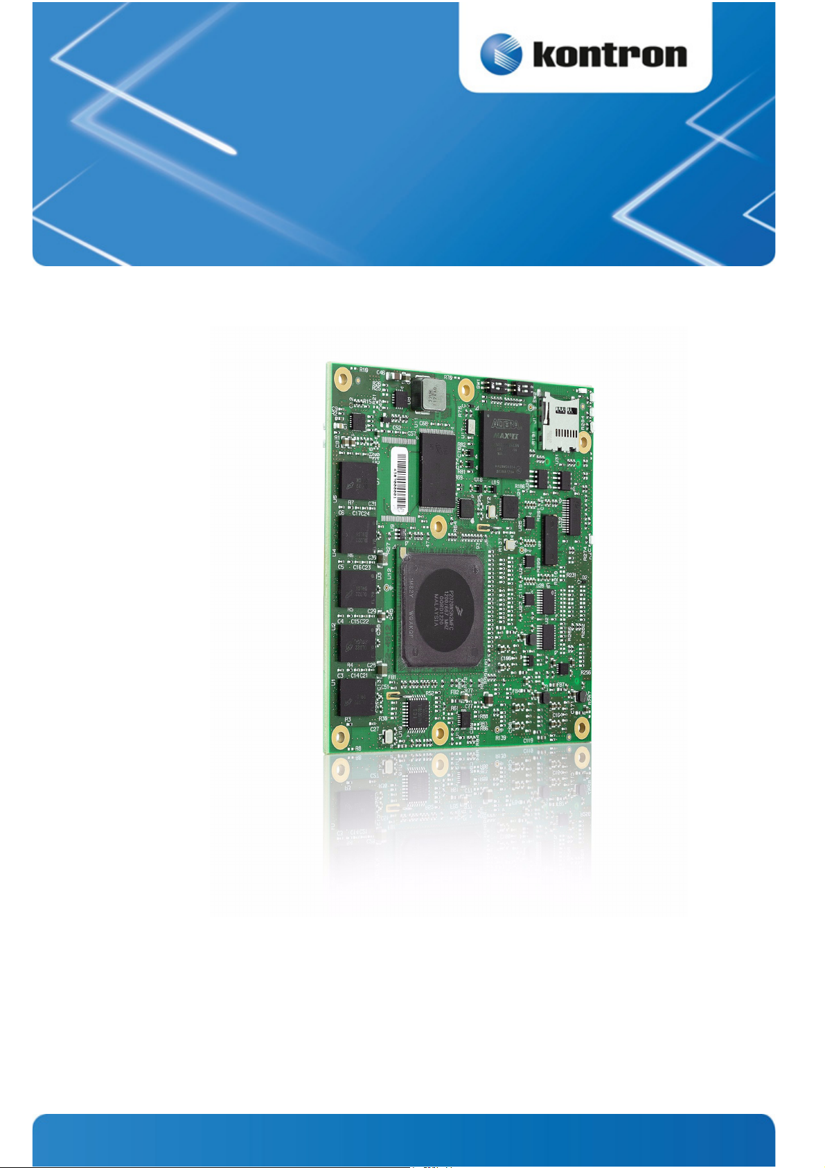
COMe-cP2020
Doc. ID: 1055-5562, Rev. 1.0
Date: September 17, 2013
www.kontron.com
Page 2

Revision History
Publication Title: COMe-P2020 User Guide
Rev. Brief Description of Changes Date of Issue
0.5 Initial Issue 18 February 2013
1.0 Chapter 3 updated 17 September 2013
Imprint
Kontron Europe GmbH may be contacted via the following:
COMe-P2020 User Guide
MAILING ADDRESS TELEPHONE AND E-MAIL
Kontron Europe GmbH +49 (0) 800-SALESKONTRON
Sudetenstraße 7 sales@kontron.com
D - 87600 Kaufbeuren Germany
For further information about other Kontron products, please visit our Internet web site: www.kontron.com.
Disclaimer
Copyright © 2013 Kontron AG. All rights reserved. All data is for information purposes only and not guaranteed for legal purposes. Information has been carefully checked and is believed to be accurate; however, no responsibility is assumed for inaccuracies. Kontron and
the Kontron logo and all other trademarks or registered trademarks are the property of their respective owners and are recognized. Specifications are subject to change without notice.
2
www.kontron.com
Page 3

COMe-P2020 User Guide
Contents
Revision History .................................................................................................................2
Imprint.............................................................................................................................2
Disclaimer .........................................................................................................................2
Proprietary Note.................................................................................................................9
Trademarks........................................................................................................................9
Environmental Protection Statement ......................................................................................9
General Instructions on Usage...............................................................................................9
Two Year Warranty...............................................................................................................9
1 Introduction ............................................................................................................. 11
1.1 COMe-cP2020 Overview ...................................................................................... 11
1.2 Board Diagrams ................................................................................................ 12
1.3 Technical Specifications ..................................................................................... 14
1.4 Standards....................................................................................................... 17
1.5 Related Publications.......................................................................................... 18
2 Functional Description ................................................................................................ 19
2.1 Processor ........................................................................................................ 19
2.2 Memory........................................................................................................... 19
2.2.1 DDR3 ......................................................................................................... 19
2.2.2 Flash Memory .............................................................................................. 19
2.2.3 System/User Data EEPROMs ............................................................................ 20
2.3 Timer.............................................................................................................. 20
2.4 Watchdog Timer................................................................................................ 20
2.5 Connectors ...................................................................................................... 21
2.5.1 COM Express Connectors ................................................................................ 21
2.5.2 Signal Descriptions COM Express Connectors ...................................................... 33
2.5.3 JTAG/Debug Interface ................................................................................... 36
3 Configuration ............................................................................................................ 38
3.1 DIP Switch Configuration.................................................................................... 38
3.2 Board Memory Map............................................................................................ 39
3.3 I/O Address Map ............................................................................................... 40
3.4 Board Control and Status Registers....................................................................... 43
4 Power Considerations.................................................................................................. 74
4.1 Electrical Specifications ..................................................................................... 74
4.1.1 Supply Voltage............................................................................................. 74
4.2 Power Supply Rise Time ...................................................................................... 74
3
www.kontron.com
Page 4

COMe-P2020 User Guide
4.3 Supply Voltage Ripple ........................................................................................ 74
4.4 Power Consumption........................................................................................... 74
5 Thermal.................................................................................................................... 76
5.1 Cooling Solution COMe-cP2020c .......................................................................... 76
5.2 Cooling Solution COMe-cP2020i ........................................................................... 77
6 U-Boot..................................................................................................................... 78
6.1 Introduction to U-Boot ...................................................................................... 78
6.2 Standard U-Boot Commands ............................................................................... 78
6.3 Kontron-Specific Commands ............................................................................... 81
6.4 U-Boot Access and Startup.................................................................................. 90
6.5 Working with U-Boot ......................................................................................... 90
6.5.1 General Operation ........................................................................................ 90
6.5.2 Using the sconf Command .............................................................................. 90
6.5.3 Examples of sconf Command Usage .................................................................. 91
6.5.4 Using the Network ........................................................................................ 94
6.5.5 Using SD Cards............................................................................................. 95
6.5.6 Using USB Devices ........................................................................................ 95
6.5.7 Using the Onboard NAND Flash........................................................................ 96
6.5.8 Using the SPI Flash for OS .............................................................................. 97
6.5.9 Booting an OS.............................................................................................. 97
6.6 Getting Help .................................................................................................... 99
6.7 Update ........................................................................................................... 99
6.8 Recovery Mechanism ........................................................................................ 100
6.9 Copyrights and Licensing................................................................................... 100
6.10 Obtaining Source Code...................................................................................... 104
7 Installation.............................................................................................................. 105
7.1 Safety............................................................................................................ 105
7.2 General Instructions on Usage ............................................................................ 105
7.3 COM Express Module-to-Carrier Assembly Considerations ......................................... 105
4
www.kontron.com
Page 5

COMe-P2020 User Guide
List of Tables
Table 1-1: COMe-cP2020 Main Specifications ..................................................................... 14
Table 1-2: Standards..................................................................................................... 17
Table 1-3: Related Publications....................................................................................... 18
Table 2-1: Connector J1 Row A Pinout .............................................................................. 21
Table 2-2: Connector J1 Row B Pinout .............................................................................. 24
Table 2-3: Connector J2 Row C Pinout............................................................................... 27
Table 2-4: Connector J2 Row D Pinout .............................................................................. 30
Table 2-5: General Signal Description............................................................................... 32
Table 2-6: P2020 SerDes Lane Routing.............................................................................. 33
Table 2-7: SerDes Protocol Mapping ................................................................................. 34
Table 2-8: SPI Signal Configurations ................................................................................ 35
Table 2-9: On-Board Device Resource ............................................................................... 35
Table 2-10: JTAG/Debug Connector J4 Pinout ...................................................................... 37
Table 3-1: DIP Switch SW1 Configuration........................................................................... 38
Table 3-2: COMe-bP2020 Virtual and Physical Memory Address Map ........................................ 39
Table 3-3: I/O Address Map ............................................................................................ 40
Table 3-4: 0x000: User Boot ROM Location Configuration Register ......................................... 43
Table 3-5: 0x001: User Host/Agent Configuration Register ................................................... 44
Table 3-6: 0x002: User I/O Port Selection Register.............................................................. 45
Table 3-7: 0x003: User Boot Configuration Register ............................................................ 46
Table 3-8: 0x004: User Boot Sequencer Configuration Register.............................................. 46
Table 3-9: 0x005: User SerDes Reference Clock Configuration Register.................................... 46
Table 3-10: 0x006: User eTSEC2 SGMII Mode Configuration Register......................................... 47
Table 3-11: 0x007: User eTSEC3 SGMII Mode Configuration Register......................................... 47
Table 3-12: 0x008: User eTSEC1 Width Configuration Register................................................. 47
Table 3-13: 0x009: User eTSEC2 Protocol Configuration Register ............................................. 48
Table 3-14: 0x00A: User eTSEC3 Protocol Configuration Register ............................................. 48
Table 3-15: 0x00B: User RapidIO Device ID Register .............................................................. 49
Table 3-16: 0x00C: User RapidIO System Size Register ........................................................... 49
Table 3-17: 0x00D: User Core0 Speed Register ..................................................................... 49
Table 3-18: 0x00E: User Core1 Speed Register ..................................................................... 50
Table 3-19: 0x00F: User SerDes OLL Time-out Enable Register ................................................. 50
Table 3-20: 0x010: Serdes Multiplexer Control Register ......................................................... 51
5
www.kontron.com
Page 6

COMe-P2020 User Guide
Table 3-21: 0x011: User Checksum Register......................................................................... 51
Table 3-22: 0x012: UFM Erase Control Register .................................................................... 51
Table 3-23: 0x013: UFM/CPU Control and Status Register....................................................... 52
Table 3-24: 0x080: POST Code Low Byte Register .................................................................. 52
Table 3-25: 0x081: POST Code High Byte Register ................................................................. 52
Table 3-26: 0x084: Debug Low Byte Register ....................................................................... 52
Table 3-27: 0x085: Debug High Byte Register ...................................................................... 53
Table 3-28: 0x280: Status Register 0.................................................................................. 53
Table 3-29: 0x282: Control Register 0 ................................................................................ 53
Table 3-30: 0x284: Device Protection Register ..................................................................... 54
Table 3-31: 0x285: Reset Status Register ............................................................................ 54
Table 3-32: 0x286: Board Interrupt Configuration Register (not implemented!) ......................... 54
Table 3-33: 0x288: Board ID High Byte Register ................................................................... 55
Table 3-34: 0x289: Board and PLD Revision Register ............................................................. 55
Table 3-35: 0x28C: Watchdog Timer Register ....................................................................... 56
Table 3-36: 0x28D: Board ID Low Byte Register .................................................................... 56
Table 3-37: 0x290: LED Configuration Register .................................................................... 57
Table 3-38: 0x291: LED Control Register ............................................................................. 57
Table 3-39: 0x300: Default Boot ROM Location Configuration Register...................................... 58
Table 3-40: 0x301: Default Host/Agent Configuration Register ............................................... 58
Table 3-41: 0x302: Default I/O Selection Register ................................................................ 59
Table 3-42: 0x303: Default Boot Configuration Register......................................................... 60
Table 3-43: 0x304: Default Boot ROM Location Configuration Register...................................... 60
Table 3-44: 0x305: Default SerDes Reference Clock Configuration Register ................................ 60
Table 3-45: 0x306: Default eTSEC2 SGMII Mode Configuration Register ..................................... 61
Table 3-46: 0x307: Default eTSEC3 SGMII Mode Configuration Register ..................................... 61
Table 3-47: 0x308: Default eTSEC1 Width Configuration Register ............................................. 61
Table 3-48: 0x309: Default eTSEC2 Protocol Configuration Register (Reserved, See note!) ............ 62
Table 3-49: 0x30A: Default eTSEC3 Protocol Configuration Register (Reserved, See note!) ............ 62
Table 3-50: 0x30B: Default RapidIO Device ID Register .......................................................... 63
Table 3-51: 0x30C: Default RapidIO System Size Register ....................................................... 63
Table 3-52: 0x30D: Default Core0 Speed Register ................................................................. 63
Table 3-53: 0x30E: Default Core1 Speed Register (Reserved, see note!).................................... 64
Table 3-54: 0x30F: Default SerDes PLL Time-out Enable Register.............................................. 64
Table 3-55: 0x320-0x321: Scratchpad Registers #0-#1 .......................................................... 64
6
www.kontron.com
Page 7

COMe-P2020 User Guide
Table 3-56: 0x322-0x327: Scratchpad Registers #2-#7 (Not implemented) ................................ 65
Table 3-57: 0x330: Power Status Register ........................................................................... 65
Table 3-58: 0x338: CPU Status Register .............................................................................. 65
Table 3-59: 0x339: CPU Control Register............................................................................. 66
Table 3-60: 0x33A: Board Variant Register .......................................................................... 66
Table 3-61: 0x350: PCIe Status Register ............................................................................. 66
Table 3-62: 0x351: PCIe Control/Status Register .................................................................. 67
Table 3-63: 0x370: Carrier Interrupt Direction Register.......................................................... 67
Table 3-64: 0x374: Carrier Interrupt Mode 1 Register ............................................................ 68
Table 3-65: 0x375: Carrier Interrupt Mode 2 Register ............................................................ 68
Table 3-66: 0x376: Board Interrupt Pending Register 1.......................................................... 69
Table 3-67: 0x377: Board Interrupt Pending Register 2.......................................................... 69
Table 3-68: 0x378: Board Interrupt Pending Register 3.......................................................... 70
Table 3-69: 0x379: Board Interrupt Pending Register 4.......................................................... 70
Table 3-70: 0x37A: Board Interrupt Enable Register 1 ........................................................... 70
Table 3-71: 0x37B: Board Interrupt Enable Register 2 ........................................................... 71
Table 3-72: 0x37C: Board Interrupt Enable Register 3............................................................ 71
Table 3-73: 0x37D: Board Interrupt Enable Register 4 ........................................................... 72
Table 3-74: 0x380: Interrupt Multiplexer Register 1 .............................................................. 72
Table 3-75: 0x381: Interrupt Multiplexer Register 2 .............................................................. 72
Table 3-76: 0x390: Carrier Control Register ......................................................................... 73
Table 4-1: Supply Voltages ............................................................................................. 74
Table 4-2: Workload Dependency..................................................................................... 74
Table 4-3: Power Consumption vs. Ambient Temperature (Standard Board Variant).................... 74
Table 4-4: Power Consumption vs. Ambient Temperature (Extended Temperature Board Variant).. 75
Table 6-1: Standard U-Boot Commands Configured for the COMe-cP2020................................. 78
Table 6-2: Kontron-Specific Commands............................................................................. 81
Table 6-3: flsw Command ............................................................................................... 82
Table 6-4: kboardinfo Command...................................................................................... 83
Table 6-5: md5sum Command ......................................................................................... 84
Table 6-6: sconf Command ............................................................................................. 85
Table 6-7: tlbdbg Command............................................................................................ 88
Table 6-8: vpd Command................................................................................................ 89
Table 6-9: Naming Conventions....................................................................................... 98
7
www.kontron.com
Page 8

COMe-P2020 User Guide
List of Figures
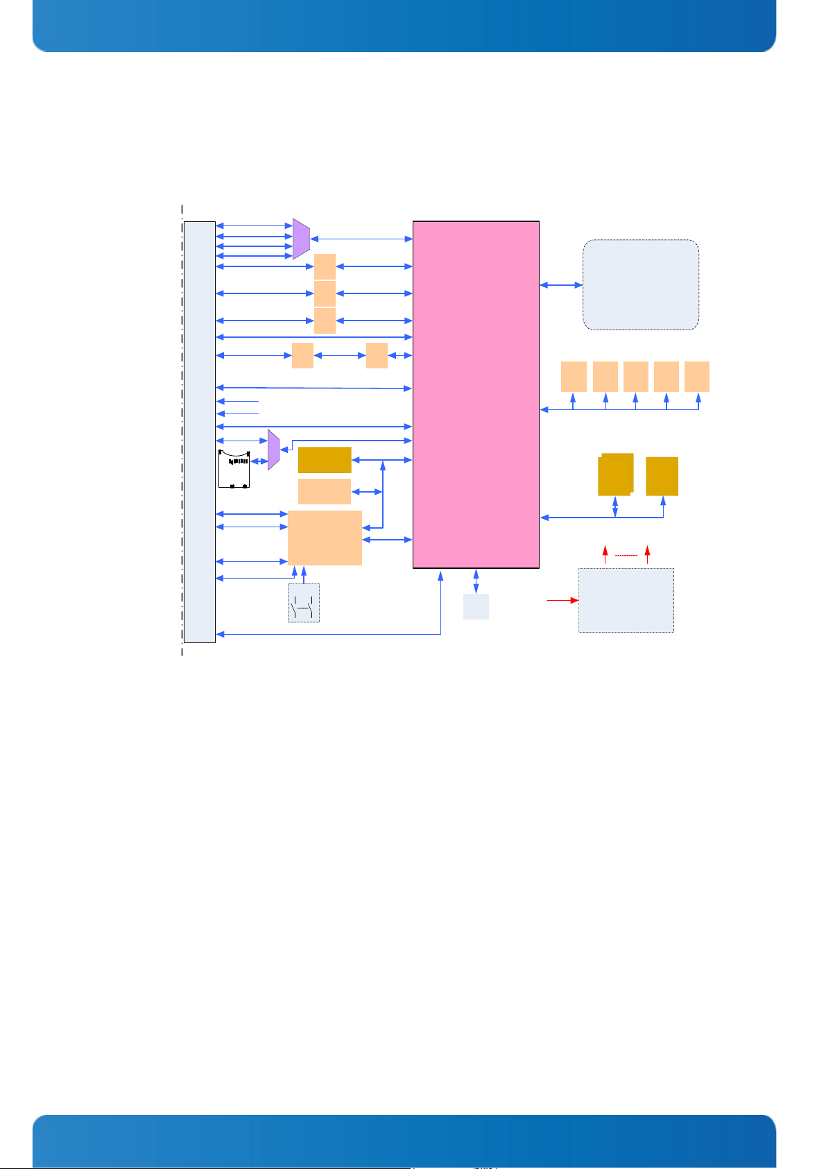
Figure 1-1: COMe-cP2020 Block Diagram ................................................................................. 12
Figure 1-2: COMe-cP2020 Board Layout Top View ...................................................................... 13
Figure 1-3: COMe-cP2020 Board Layout Bottom View ................................................................. 13
Figure 2-1: IRQ Routing Scheme ............................................................................................ 36
Figure 5-1: Cooling Solution COMe-cP2020c............................................................................. 76
Figure 5-2: Cooling Solution COMe-cP2020i ............................................................................. 77
8
www.kontron.com
Page 9

COMe-P2020 User Guide
Proprietary Note
This document contains information proprietary to Kontron. It may not be copied or transmitted by any means, disclosed to
others, or stored in any retrieval system or media without the prior written consent of Kontron or one of its authorized
agents.
The information contained in this document is, to the best of our knowledge, entirely correct. However, Kontron cannot
accept liability for any inaccuracies or the consequences thereof, or for any liability arising from the use or application of
any circuit, product, or example shown in this document.
Kontron reserves the right to change, modify, or improve this document or the product described herein, as seen fit by Kontron without further notice.
Trademarks
Kontron and the Kontron logo are trade marks owned by Kontron AG, Germany. In addition, this document may include
names, company logos and trademarks, which are registered trademarks and, therefore, proprietary to their respective
owners.
Environmental Protection Statement
This product has been manufactured to satisfy environmental protection requirements where possible. Many of the com-
ponents used (structural parts, printed circuit boards, connectors, batteries, etc.) are capable of being recycled.
Final disposition of this product after its service life must be accomplished in accordance with applicable country, state, or
local la
ws or regulations.
General Instructions on Usage
In order to maintain Kontron’s product warranty, this product must not be altered or modified in any way. Changes or mod-
ifications to the device, which are not explicitly approved by Kontron and described in this manual or received from Kontron’s Technical Support as a special handling instruction, will void your warranty.
This device should only be installed in or connected to systems that fulfill all necessary technical and specific environmental requirements. This applies also to the operational temperature range of the specific system version, which must not be
exceeded. If batteries are present their temperature restrictions must be taken into account.
In performing all necessary installation and application operations, please follow only the instructions supplied by the
present manual.
Keep all the original packaging material for future storage or warranty shipments. If it is necessary to store or ship the system, please re-pack it as nearly as possible in the manner in which it was delivered.
Special care is necessary when handling or unpacking the product. Please consult the special handling and unpacking
instruction on the previous page of this manual.
Two Year Warranty
Kontron grants the original purchaser of Kontron’s products a TWO YEAR LIMITED HARDWARE WARRANTY as described in the following. However, no other warranties that may be granted or implied by anyone on behalf of Kontron are valid unless the consumer has the express written consent of Kontron.
Kontron warrants their own products, excluding software, to be free from manufacturing and material defects for a period
of 24 consecutive months from the date of purchase. This warranty is not transferable nor extendible to cover any other
users or long-term storage of the product. It does not cover products which have been modified, altered or repaired by any
other party than Kontron or their authorized agents. Furthermore, any product which has been, or is suspected of being
damaged as a result of negligence, improper use, incorrect handling, servicing or maintenance, or which has been damaged as a result of excessive current/voltage or temperature, or which has had its serial number(s), any other markings or
parts thereof altered, defaced or removed will also be excluded from this warranty.
If the customer’s eligibility for warranty has not been voided, in the event of any claim, he may return the product at the
earliest possible convenience to the original place of purchase, together with a copy of the original document of purchase,
a full description of the application the product is used on and a description of the defect. Pack the product in such a way as
to ensure safe transportation (see our safety instructions).
9
www.kontron.com
Page 10

COMe-P2020 User Guide
Kontron provides for repair or replacement of any part, assembly or sub-assembly at their own discretion, or to refund the
original cost of purchase, if appropriate. In the event of repair, refunding or replacement of any part, the ownership of the
removed or replaced parts reverts to Kontron, and the remaining part of the original guarantee, or any new guarantee to
cover the repaired or replaced items, will be transferred to cover the new or repaired items. Any extensions to the original
guarantee are considered gestures of goodwill, and will be defined in the “Repair Report” issued by Kontron with the
repaired or replaced item.
Kontron will not accept liability for any further claims resulting directly or indirectly from any warranty claim, other than
the above specified repair, replacement or refunding. In particular, all claims for damage to any system or process in which
the product was employed, or any loss incurred as a result of the product not functioning at any given time, are excluded.
The extent of Kontron liability to the customer shall not exceed the original purchase price of the item for which the claim
exists.
Kontron issues no warranty or representation, either explicit or implicit, with respect to its products’ reliability, fitness,
quality, marketability or ability to fulfil any particular application or purpose. As a result, the products are sold “as is,” and
the responsibility to ensure their suitability for any given task remains that of the purchaser. In no event will Kontron be
liable for direct, indirect or consequential damages resulting from the use of our hardware or software products, or documentation, even if Kontron were advised of the possibility of such claims prior to the purchase of the product or during any
period since the date of its purchase.
Please remember that no Kontron employee, dealer or agent is authorized to make any modification or addition to the
above specified terms, either verbally or in any other form, written or electronically transmitted, without the company’s
consent.
10
www.kontron.com
Page 11

COMe-P2020 User Guide
1Introduction
1.1 COMe-cP2020 Overview
The COMe-cP2020 is a COM Express® form factor compliant Power Architecture® processor module based on Freescale's
QorIQ™ 32-bit P2020 processor.
Designed in the COM Express® basic (95 mm x 95 mm) form factor the module incorporates the Freescale QorIQ P2020 dualcore Power Architecture® processor operating up to 1.2 GHz - other processor versions (P2010, P1020 and P1011) and
operating speeds are available on request. Featuring 32-bit technology, it integrates up to 4 GByte of soldered DDR3
SDRAM at 667 MHz and ECC support. 512 KBytes of shared second level cache facilitate core-to-core communications to
minimize accesses to main memory.
Up to 2 GByte of NAND Flash as well as a socket for MicroSD card offer reliable storage space for application data. In terms
of I/Os, the module interfaces the QorIQ-specific I/Os to the carrier board. In addition to USB 2.0 ports there are also UART
(TxD, RxD, RTC and CTS) and Gigabit Ethernet interfaces.
Flexible interface support is guaranteed by 4 SERDES lanes, which can be configured according to application-specific
needs. A comprehensive range of different combinations, for example as PCIe x4, sRIO x4 and Serial Gigabit Media Independent Interface (SGMII) is available.
The COMe-cP2020 targets high-bandwidth telecommunication and data processing applications. With its long-term availability of more than 10 years, it is also a good fit to be used in long life cycle network applications in the medical, military
and transportation markets.
Kontron offers two modules in standard and extended temperature range:
• COMe-cP2020c
• P2020NSN2MFC 1200 MHZ
• 2 GByte 667 MHz DDR3 Memory
•1 GByte NAND
• 0°C - 60 °C Ambient Temperature
• Standard COMe Heatspreader
• COMe-cP2020i
• P2020NXN2KFC 1000 MHZ
• 2 GByte 667 MHz DDR3 Memory
•1 GByte NAND
• -40°C - 85 °C Ambient Temperature
• Extended 95x95 mm Forced Air Cooling Heatsink
11
www.kontron.com
Page 12
1.2 Board Diagrams
SPI- NOR
FLASH
2x 8 Mb
DDR3 SDRAM
1/2/4 GB w ECC
9x DDR3 x8
1 bank solder ed
COM eP2020:COM Expressm odulebasedonQorIQP2020
Rev. 0.1
CPLD
Board Control
WDog, glue, etc.
COP/
JTAG
Debug
Freescale
Qor I Q P20 20
Dual-Core
32-bit PowerPC
up to 1.2 GHz
DDR3
RTC
RGMII
NAND FLASH
up to 2 GB
Sys
EEP
64kb
SPI
COP
Local Bus
I2C_1
SDHC
Micr oSD -Ca rd
Socket
Uboot Fl ash
redundant
SPI- NOR
Flash
64 Mb
GbE
PHY
Therm.
Sensor
User
EEP
64kb
72-bit ,
667 MHz
SPD
EEP
2kb
eTSEC 3
SPI- NOR
FLASH
16 Mb
OS Boot
ROM
2x Module Connector 0.5 mm pitch 220 pin 4H Receptacle A1-A110/B1-B110/C1-C110/D1-D110
SPI
SERDES 0- 3
SERDES 2
MDI
1x SDHC
ULPI
LAD Bus
4 DIP-SW
I2C#1
eLBC
OUT: 5V / 3.3V / 2.5V
1.5V / 1.2V / 1.05V / 0.75V
DC/DC
IN :12V
Up to 2x sRIO x1, x4
or 3x PCIe x1, x2, x4
or 2x GbE (SGMII)
GbE
USB 2.0
USB
Hub
4x USB 2.0
4x USB Hos t
2x RxD/ TxD/RTS/ CTS
1x SD-Card I/F
GPIO
ETH_Mngt 1
Local Bus
MRAM
512 KB
DUART
2x Serial
I2C_2
2x I2C
opt.
strictly confidential
SPI
SPI
MUX
SERDES 1
I2C#1
I2C#2
MDIO/MDC
ETH_Mngt 1
JTAG
JTAG
IEEE1588
IEEE1588
IEEE1588
MISC
EXP Card
EXP Card
MUX
opt.
USB
PHY
RGMII
GbE
PHY
eTSEC 2
MDI
GbE
RGMII
GbE
PHY
eTSEC 1
MDI
GbE
SERDES 3
SERDES 0,1 ,2,3
Figure 1-1: COMe-cP2020 Block Diagram
COMe-P2020 User Guide
12
www.kontron.com
Page 13
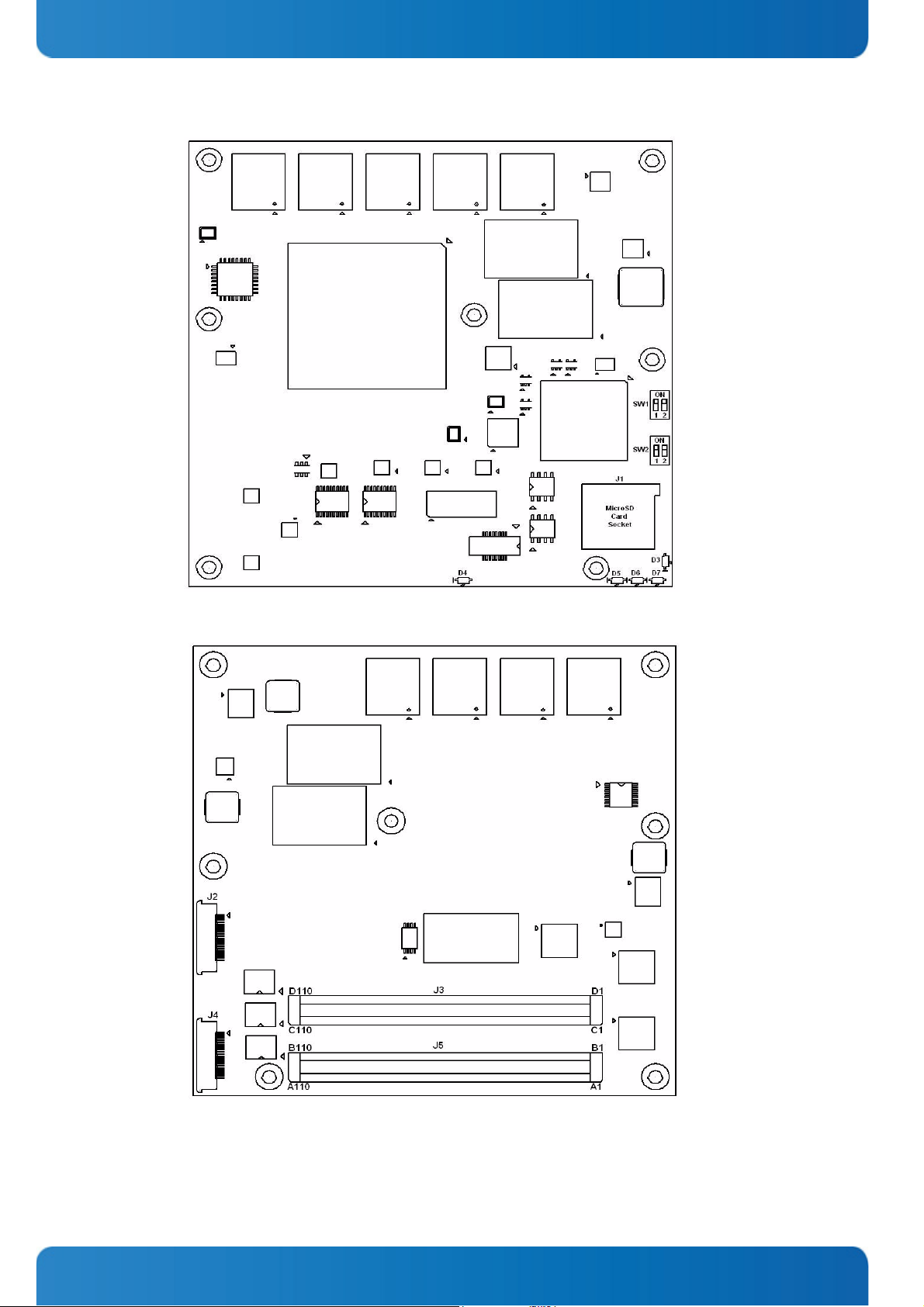
Figure 1-2: COMe-cP2020 Board Layout Top View
COMe-P2020 User Guide
Figure 1-3: COMe-cP2020 Board Layout Bottom View
13
www.kontron.com
Page 14

1.3 Technical Specifications
Table 1-1: COMe-cP2020 Main Specifications
COMe-cP2020 SPECIFICATIONS
CPU The COMe-cP2020 supports the following microprocessor:
• Freescale™ QorIQ™ P2020 processor, 1.2 GHz, 667 MHz platform frequency
standard temperature range
• Freescale™ QorIQ™ P2020 processor, 1.0 GHz, 667 MHz platform frequency extended temperature range
COMe-P2020 User Guide
PROCESSOR
available on request)
Integrated Controllers Controllers integrated in the CPU and utilized by the COMe-cP2020 are:
• eSDHC, eLBC, DUART, eTSEC, PCIe, sRIO, SPI, I²C
Memory Main memory:
• Up to 4 GB, dual-channel DDR3 SDRAM memory with ECC running at 667 MHz
(800 MHz version is available on request)
Cache structure:
• 32 kB instruction cache for each e500 core
• 32 kB data cache for each e500 core
• 512 kB shared L2 cache
Flash memory:
• Two SPI boot flashes (2 x 2 MB) for U-Boot selectable via the DIP switch
(Other operating speeds and processor variants (P2010, P1020 and P1011) are
MEMORY
• One 8 MB SPI flash for operating system or application
Mass storage device:
• Up to 2 GB NAND flash via an integrated/embedded NAND flash controller
• Up to 32 GB microSDHC flash via an integrated SDHC controller
MRAM memory:
• 512 kB of non-volatile memory
Two serial EEPROMs with 64 kbit:
• One for system data storage
14
• One free for user data storage
www.kontron.com
Page 15

Table 1-1: COMe-cP2020 Main Specifications (Continued)
COMe-cP2020 SPECIFICATIONS
Gigabit Ethernet Up to five Gigabit Ethernet ports:
• Three Gigabit Ethernet port through COMe MDI interface
• Up to two Gigabit Ethernet ports through SGMII interface
COMe-P2020 User Guide
SRIO
Serial RapidIO interfaces operate in host or agent configuration in various
speeds: 1.25 GHz, 2.5 GHz or 3.125GHz, depending on configuration
•One interface x1
•One interface x4
•Two interfaces x1
PCI Express
PCI Express interface operates in host or agent at 2.5 GHz (PCIe GEN1), depending on configuration
•One interface x1
•One interface x2
INTERCONNECTION
•One interface x4
•Two interfaces x1
•Two interfaces x2
• Three interfaces x1, x1, x2
Debug Interface One debug port
Serial Interface Up to two serial ports:
• 2x 4-wire UART interfaces (RxD, TxD, RTS, CTS)
GPIO/Interrupts Five GPIOs are shared with Interrupts. Function depends on configuration
Onboard Connectors
• Two 220-pin connectors for interfacing with a carrier board
• One JTAG/COP connector, J4, for debugging
microSD card Socket Standard microSD socket, J9, accepts microSD and microSDHC cards
Connectors
DIP Switch Two DIP switches for board configuration, SW1/SW2, consisting of two
Switch
Module Health Monitor
LEDs
LEDs
switches
CPLD HEALTY D4: indicates by blinking CPLD is active
LED0 D5:indicates U-Boot boot failure
LED1 D6: indicates CPU reset is asserted
LED2 D7: not used
LED3 D3: indicates Power-Good failure
15
www.kontron.com
Page 16

Table 1-1: COMe-cP2020 Main Specifications (Continued)
COMe-cP2020 SPECIFICATIONS
Watchdog Timer Software-configurable, two-stage Watchdog with programmable timeout
ranging from 125 ms to 4096 s in 16 steps
Serves for generating IRQ or hardware reset
TIMER
System Timer There are several timers implemented in the CPU. For further information
regarding these timers, refer to the CPU reference manual from Freescale.
Thermal Monitoring CPU and board temperature is provided by one onboard temperature sensor
for monitoring the board temperature
THERMAL
Power Consumption Refer to Chapter 5, “Power Considerations” for information related to the
power consumption of the COMe-cP2020.
COMe-P2020 User Guide
Temperature Range Operational:
• 0°C to +60°C (Standard Version)
• -40°C to +85°C (Extended Temperature Version)
Storage: -40°C to +70°C
GENERAL
Mechanical COM Express®compact
Dimensions 95 mm x 95 mm
Board Weight 99 grams (without heatspreader)
220 grams (with heatspreader)
Bootloader DENX U-Boot (Universal Boot Loader) with Kontron-specific modifications to
support the COMe-cP2020 requirements
Operating Systems The board is offered with various Board Support Packages including VxWorks
SOFTWARE
and Linux operating systems. For further information concerning the operating systems available for the COMe-cP2020, please contact Kontron.
16
www.kontron.com
Page 17

1.4 Standards
The COMe-cP2020 complies with the requirements of the following standards.
Table 1-2: Standards
COMPLIANCE TYPE STANDARD TEST LEVEL
COMe-P2020 User Guide
CE Emission EN55022
EN61000-6-3
Immission EN55024
EN61000-6-2
Electrical Safety EN60950-1 --
Railway Safety Electrical Safety EN50155 --
Mechanical Mechanical Dimensions COM Express® com-
pact
Environmental
and Health
Vibration
(sinusoidal, operating)
EN 50155
IEC 60068-2-6
Aspects
VITA 47
Shock (operating) EN 50155 Class 1B
Bump
Operating
IEC
60068-2-29
--
--
--
Class 1B
Frequency:10 - 300 Hz
Acceleration: 5 g
Class V1
5 to 100Hz
~2g RMS
Peak Accel.: 15 g
Shock Dur.: 11 ms half sine
Shock Count: 500
Climatic Humidity IEC60068-2-78 93% RH at 40°C, non-condensing
(see notice below)
WEEE Directive 2002/96/EC Waste electrical and electronic
equipment
RoHS-II Directive 2011/65/EC Restriction of the use of certain
hazardous substances in electrical and electronic equipment
17
www.kontron.com
Page 18

Kontron performs comprehensive environmental testing of its products in accordance with applicable standards.
Customers desiring to perform further environmental testing of Kontron products must contact
Kontron for assistance prior to performing any such testing. This is necessary, as it is possible
that environmental testing can be destructive when not performed in accordance with the applicable specifications.
In particular, for example, boards without conformal coating must not be exposed to a change of
temperature exceeding 1K/minute, averaged over a period of not more than five minutes. Otherwise, condensation may cause irreversible damage, especially when the board is powered up
again.
Kontron does not accept any responsibility for damage to products resulting from destructive
environmental testing.
1.5 Related Publications
COMe-P2020 User Guide
NOTICE
Table 1-3: Related Publications
SPECIFICATION /
ORGANIZATION
PUBLICATION
COM Express PICMG® COM.0, COM Express® Module Base Specification, Revision 2.0, August 8, 2010
Freescale, Kontron and Emerson Common Pinout Definition
PCI Express PCI Express Base Specification Revision 2.0, Dec. 20, 2006
Serial RapidIO
RapidIO
™ Interconnect Specification Part 6: LP-Serial Physical Layer Specification,
Rev. 2.0.1, March 2008
Ethernet IEEE802.3: Part 3: Carrier Sense Multiple Access with Collision Detection (CSMA/CD)
Access Method and Physical Layer Specification, Clause 22
Platform Firmware DENX “U-Boot” (Universal Boot Loader) online documentation at www.denx.de
Kontron Kontron’s Product Safety and Implementation Guide, ID 1021-9142
18
www.kontron.com
Page 19

COMe-P2020 User Guide
2 Functional Description
2.1 Processor
The COMe-cP2020 supports the high-performance, 32-bit, 45nm dual-core Freescale QorIQ P2020 processor with the following functions and features:
• Two e500v2 cores built on Power Architecture technology, running up to 1.2 GHz clock speed
• 512 Kbyte shared level two cache
• One 64-bit DDR3 SDRAM memory controllers with ECC and chip-select interleaving support
• Data path acceleration architecture incorporating acceleration for Packet-/Buffer- and Queue-Management
• Three 1 Gbps Ethernet controllers
• Up to three PCI Express 1.0a controllers/ports running at 2.5 Gbps
• Two serial RapidIO controllers/ports version 1.2 running at up to 3.125 Gbps
• One ULPI controller
• One SD/MMC controller
• One SPI controller
• Two I2C controllers
• Two DUARTs
• One enhanced local bus controller
• Multicore programmable interrupt controller
2.2 Memory
2.2.1 DDR3
The COMe-cP2020 supports a soldered, single-channel (72-bit), Double Data Rate (DDR3) memory with Error Checking and
Correcting (ECC) running at up to 800 MHz (memory error detection and reporting of 1-bit and 2-bit errors and correction
of 1-bit failures). The available memory configuration can be either 1 GB, 2 GB or 4 GB.
2.2.2 Flash Memory
2.2.2.1 SPI Boot Flash
The COMe-cP2020 provides two 2 MB SPI boot flashes for two separate U-Boot images, a standard SPI boot flash and a
recovery SPI boot flash. The fail-over mechanism for the U-Boot recovery can be controlled via the DIP switch SW1, switch
1. Refer to Chapter 6.10 for further information.
The SPI boot flashes include a hardware write protection option. If write protection is enabled, writing to the SPI boot
flashes is not possible.
N O T I C E
19
The U-Boot code and settings are stored in the SPI boot flashes. Changes made to the U-Boot settings are available only in the currently selected SPI boot flash. Thus, switching over to the other
SPI boot flash may result in operation with different U-Boot code and settings.
www.kontron.com
Page 20

COMe-P2020 User Guide
2.2.2.2 SPI OS/User Flash
The COMe-cP2020 supports 8 MB of soldered flash memory for the OS.
2.2.2.3 NAND Flash
The COMe-cP2020 supports up to 2 GB of soldered NAND flash memory, which is an SLC-based NAND flash. It is optimized for
embedded systems providing high performance, reliability and security.
2.2.2.4 MRAM Memory
The COMe-cP2020 supports 512 kB of MRAM memory (Magnetorestrictive Random Access Memory) for fast non-volatile
data storage (optional).
2.2.2.5 SDHC Socket
The COMe-cP2020 is provided with a microSDHC card socket, J1, which accepts microSD and microSDHC cards up to 32 GB. If
used, the card must be installed prior to installation of the COMe-cP2020 in a system.
If the SDHC interface is routed to the COM Express connector (via DIP switch SW1, switch [1]), the onboard socket J1 cannot
be used.
2.2.3 System/User Data EEPROMs
The COMe-cP2020 provides two 64-kBit EEPROMs, one for system data storage and one which is free for user data storage.
The user data EEPROM is accessible via the OS or an application. The system data EEPROM is reserved for system usage.
2.3 Timer
The COMe-cP2020 is equipped with the following timer:
• Real-Time Clock (RTC)
The COMe-cP2020 is equipped with an onboard high-precision real-time clock RV-8564-C3. The RV-8564-C3 RTC is registercompatible with the PCF8564A RTC from Philips/NXP. In addition, it provides a very tight frequency tolerance at low power
consumption. The COMe-cP2020 does not include a 3 V lithium battery or a GoldCap power source for RTC backup. Power for
the RTC is supplied by the carrier via the VCC_RTC pin.
2.4 Watchdog Timer
The COMe-cP2020 provides a Watchdog timer that is programmable for a timeout period ranging from 125 ms to 4096 s in
16 steps. Failure to trigger the Watchdog timer in time results in a interrupt or a system reset or both. In dual-stage mode,
it results in a combination of both interrupt and reset if the Watchdog is not serviced. A hardware status flag will be provided to determine if the Watchdog timer generated the reset. Refer to the Watchdog Timer Control Register (WTIM) in
Chapter 3 for further information.
There are four possible modes of operation involving the Watchdog timer:
• Timer only mode
• Reset mode
• Interrupt mode
• Dual stage mode
At power on the Watchdog is not enabled. If required, the bits of the Watchdog Timer Control Register must be set according
to the application requirements. To operate the Watchdog, the mode and time period required must first be set and then
the Watchdog enabled. Once enabled, the Watchdog can only be disabled or the mode changed by powering down and then
up again. To prevent a Watchdog timeout, the Watchdog must be retriggered before timing out. This is done by writing a ‘1’
to the WTR bit. In the event a Watchdog timeout does occur, the WTE bit is set to ‘1’. What transpires after this depends on
the mode selected.
20
www.kontron.com
Page 21

COMe-P2020 User Guide
The four operational Watchdog timer modes can be configured by the WMD[1:0] bits, and are described as follows:
Timer only mode - In this mode the Watchdog is enabled using the required timeout period. Normally, the Watchdog is
retriggered by writing a ‘1’ to the WTR bit. In the event a timeout occurs, the WTE bit is set to ‘1’. This bit can then be polled
by the application and handled accordingly. To continue using the Watchdog, write a ‘1’ to the WTE bit, and then retrigger
the Watchdog using WTR. The WTE bit retains its setting as long as no power down-up is done. Therefore, this bit may be
used to verify the status of the Watchdog.
Reset mode - This mode is used to force a hard reset in the event of a Watchdog timeout. In addition, the WTE bit is not reset
by the hard reset, which makes it available if necessary to determine the status of the Watchdog prior to the reset.
Interrupt mode - This mode causes the generation of an interrupt in the event of a Watchdog timeout. The interrupt handling is a function of the application. If required, the WTE bit can be used to determine if a Watchdog timeout has occurred.
Dual stage mode - This is a complex mode where in the event of a timeout two things occur: 1) an interrupt is generated,
and 2) the Watchdog is retriggered automatically. In the event a second timeout occurs following the first timeout, a hard
reset will be generated. The second timeout period is the same as the first. If the Watchdog is retriggered normally as specified above, operation continues. The interrupt generated at the first timeout is available to the application to handle the
first timeout if required. As with all of the other modes, the WTE bit is available for application use.
Pin B27 on the COM Express® J1 connector offers a signal that can be asserted when a Watchdog timer has not been triggered within time. It can be configured to any of the 2 stages. Deassertion of the signal is automatically done after reset. If
deassertion during runtime is necessary please contact Kontron for further assistance.
2.5 Connectors
2.5.1 COM Express Connectors
Table 2-1: Connector J1 Row A Pinout
PIN SIGNAL
A1 GND PWR GND
A2 GBE0_MDI3- GigE MDI DP-I/O eTSEC1_GBE0_MDI3-
A3 GBE0_MDI3+ GigE MDI DP-I/O eTSEC1_GBE0_MDI3+
A4 GBE0_LINK100# GigE MDI O-3.3 eTSEC1_GBE0_LINK100#
A5 GBE0_LINK1000# GigE MDI O-3.3 eTSEC1_GBE0_LINK1000#
A6 GBE0_MDI2- GigE MDI DP-I/O eTSEC1_GBE0_MDI2-
A7 GBE0_MDI2+ GigE MDI DP-I/O eTSEC1_GBE0_MDI2+
A8 GBE0_LINK# GigE MDI O-3.3 eTSEC1_GBE0_LINK#
A9 GBE0_MDI1- GigE MDI DP-I/O eTSEC1_GBE0_MDI1-
A10 GBE0_MDI1+ GigE MDI DP-I/O eTSEC1_GBE0_MDI1+
A11 GND PWR GND
A12 GBE0_MDI0- GigE MDI DP-I/O eTSEC1_GBE0_MDI0-
A13 GBE0_MDI0+ GigE MDI DP-I/O eTSEC1_GBE0_MDI0+
A14 GBE0_CTREF GigE MDI Not applicable
A15 SUS_S3# BOARD CTRL O-3.3 Undefined
A16 SATA0_TX+ SATA N/C
A17 SATA0_TX- SATA N/C
A18 SUS_S4# BOARD CTRL O-3.3 Undefined
A19 SATA0_RX+ SATA N/C
A20 SATA0_RX- SATA N/C
A21 GND PWR GND
A22 SATA2_TX+ SATA N/C
A23 SATA2_TX- SATA N/C
A24 SUS_S5# BOARD CTRL O-3.3 Undefined
A25 SATA2_RX+ SATA N/C
A26 SATA2_RX- SATA N/C
SIGNAL
GROUP
TYPE TERMINATION COMMENT
21
www.kontron.com
Page 22

COMe-P2020 User Guide
Table 2-1: Connector J1 Row A Pinout (Continued)
PIN SIGNAL
A27 BATLOW# BOARD CTRL I-3.3 Interrupt Source
A28 (S)ATA_ACT# SATA N/C
A29 AC/HAD_SYNC AUDIO N/C
A30 AC/HAD_RST# AUDIO N/C
A31 GND PWR GND
A32 AC/HAD_BITCLK AUDIO N/C
A33 AC/HAD_SDOUT AUDIO N/C
A34 BIOS_DIS0# BOARD CTRL I-3.3 N/C
A35 THERMTRIP# BOARD CTRL O-3.3 THERMTRIP#
A36 USB6- USB2.0 N/C
A37 USB6+ USB2.0 N/C
A38 USB_6_7_OC# USB2.0 N/C
A39 USB4- USB2.0 N/C
A40 USB4+ USB2.0 N/C
A41 GND PWR GND
A42 USB2- USB2.0/
A43 USB2+ USB2.0/
A44 USB_2_3_OC# USB2.0/
A45 USB0- USB2.0/
A46 USB0+ USB2.0/
A47 VCC_RTC PWR 3V VCC_RTC
A48 EXCD0_PERST# EXP CARD O-3.3 Undefined
A49 EXCD0_CPPE# EXP CARD I-3.3 Undefined
A50 RSVD Local Bus O-3.3 LA16
A51 GND PWR GND
A52 SERDES_TX5+ SERDES N/C
A53 SERDES_TX5- SERDES N/C
A54 GPIO/SD_DATA0 GPIO/SDIO I/O-3.3 SD_DATAO
A55 SERDES_TX4+ SERDES DP-O MUX_PCIE_TX1_P
A56 SERDES_TX4- SERDES DP-O MUX_PCIE_TX1_N
A57 GND PWR GND
A58 SERDES_TX3+ SERDES DP-O SERDES_TX3+
A59 SERDES_TX3- SERDES DP-O SERDES_TX3-
A60 GND PWR GND
A61 SERDES_TX2+ SERDES DP-O SERDES_TX2+
A62 SERDES_TX2- SERDES DP-O SERDES_TX2-
A63 GPI1/SD_DATA1 GPIO/SDIO I/O-3.3 SD_DATA1
A64 SERDES_TX1+ SERDES DP-O SERDES_TX1+
A65 SERDES_TX1- SERDES DP-O SERDES_TX1-
A66 GND PWR GND
A67 GPI2/SD_DATA2 GPIO/SDIO I/O-3.3 SD_DATA2
A68 SERDES_TX0+ SERDES DP-O SERDES_TX0+
A69 SERDES_TX0- SERDES DP-O SERDES_TX0-
A70 GND PWR GND
SIGNAL
GROUP
USB3.0
USB3.0
USB3.0
USB3.0
USB3.0
TYPE TERMINATION COMMENT
USB2-
USB2+
I-3.3 USB_2_3_OC#
DP-I/O USB0-
DP-I/O USB0+
22
www.kontron.com
Page 23

COMe-P2020 User Guide
Table 2-1: Connector J1 Row A Pinout (Continued)
PIN SIGNAL
A71 LVDS_A0+ LVDS RSVD
A72 LVDS_A0- LVDS RSVD
A73 LVDS_A1+ LVDS RSVD
A74 LVDS_A1- LVDS RSVD
A75 LVDS_A2+ LVDS RSVD
A76 LVDS_A2- LVDS RSVD
A77 LVDS_VDD_EN LVDS RSVD
A78 LVDS_A3+ LVDS RSVD
A79 LVDS_A3- LVDS RSVD
A80 GND PWR GND
A81 LVDS_A_CK+ LVDS RSVD
A82 LVDS_A_CK- LVDS RSVD
A83 LVDS_I2C_CK LVDS RSVD
A84 LVDS_I2C_DAT LVDS RSVD
A85 GPI3/SD_DATA3 GPIO/SDIO I/O-3.3 SD_DATA3
A86 RSVD19 Local Bus O-3.3 LA18
A87 RSVD19 Local Bus O-3.3 LA17
A88 SERDES_CK_REF1+ SERDES O-3.3 SERDES_CK_REF+
A89 SERDES_CK_REF1- SERDES O-3.3 SERDES_CK_REF-
A90 GND PWR GND
A91 SPI_POWER SPI O-3.3 3.3V Source for carrier SPI flash
A92 SPI_MISO SPI I-3.3 SPI_MISO
A93 GPO0/SD_CLK GPIO/SDIO O-3.3 SD_CLK
A94 SPI_CLK SPI SPI_CLK
A95 SPI_MOSI SPI O-3.3 SPI_MOSI
A96 TPM_PP BOARD CTRL GND
A97 TYPE10# TYPE Single 4K7 pull down, DNI
A98 SER0_TX UART O-3.3 U0_TXD
A99 SER0_RX UART I-3.3 U0_RXD
A100 GND PWR GND
A101 SER1_TX UART O-3.3 U1_TXD
A102 SER1_RX UART I-3.3 U1_RXD
A103 LID# BOARD CTRL N/C
A104 VCC_12V PWR VCC_12V
A105 VCC_12V PWR VCC_12V
A106 VCC_12V PWR VCC_12V
A107 VCC_12V PWR VCC_12V
A108 VCC_12V PWR VCC_12V
A109 VCC_12V PWR VCC_12V
A110 GND PWR GND
SIGNAL
GROUP
TYPE TERMINATION COMMENT
23
www.kontron.com
Page 24

COMe-P2020 User Guide
Table 2-2: Connector J1 Row B Pinout
PIN SIGNAL
B1 GND PWR
B2 GBE0_ACT# GigE MDI
B3 1588_CLK_OUT IEEE1588 O-3.3 1588_CLK_OUT
B4 1588_PULSE_OUT1 IEEE1588 O-3.3 1588_PULSE_OUT1
B5 1588_PULSE_OUT2 IEEE1588 O-3.3 1588_PULSE_OUT2
B6 1588_ALARM_OUT1 IEEE1588 O-3.3 1588_ALARM_OUT1
B7 1588_ALARM_OUT2 IEEE1588 O-3.3 1588_ALARM_OUT2
B8 1588_TRIG_IN1 IEEE1588 I-3.3 1588_TRIG_IN1
B9 1588_TRIG_IN2 IEEE1588 I-3.3 1588_TRIG_IN2
B10 1588_CLK_IN IEEE1588 I-3.3 1588_CLK_IN
B11 GND PWR GND
B12 PWRBTN# BOARD CTRL I-3.3 Undefined
B13 SMB_CK SMB I/O-3.3 SMB_CK
B14 SMB_DAT SMB I/O-3.3 SMB_DAT
B15 SMB_ALERT# SMB 3.3 Interrupt Source
B16 SATA1_TX+ SATA N/C
B17 SATA1_TX- SATA N/C
B18 SUS_STAT# BOARD CTRL O-3.3 N/C
B19 SATA1_RX+ SATA N/C
B20 SATA1_RX- SATA N/C
B21 GND PWR GND
B22 SATA3_TX+ SATA N/C
B23 SATA3_TX- SATA N/C
B24 PWR_OK BOARD CTRL I-3.3 PWR_OK
B25 SATA3_RX+ SATA N/C
B26 SATA3_RX- SATA N/C
B27 WDT BOARD CTRL WDT
B28 AC/HAD_SDIN2 AUDIO N/C
B29 AC/HAD_SIN1 AUDIO N/C
B30 AC/HAD_SIN0 AUDIO N/C
B31 GND PWR GND
B32 SPKR BOARD CTRL N/C
B33 I2C_CK I2C I/O-3.3 I2C_CK
B34 I2C_DAT I2C I/O-3.3 I2C_DAT
B35 THERM# BOARD CTRL I-3.3 Interrupt Source
B36 USB7- USB2.0 N/C
B37 USB7+ USB2.0 N/C
B38 USB_4_5_OC# USB2.0 N/C
B39 USB5- USB2.0 N/C
B40 USB5+ USB2.0 N/C
B41 GND PWR GND
B42 USB3- USB2.0/
B43 USB3+ USB2.0/
B44 USB_0_1_OC# USB2.0/
SIGNAL
GROUP
USB3.0
USB3.0
USB3.0
TYPE TERMINATION COMMENT
USB3-
USB3+
I-3.3 USB_0_1_OC#
24
www.kontron.com
Page 25

COMe-P2020 User Guide
Table 2-2: Connector J1 Row B Pinout (Continued)
PIN SIGNAL
B45 USB1- USB2.0/
B46 USB1+ USB2.0/
B47 EXCD1_PERST# EXP CARD O-3.3 Undefined
B48 EXCD1_CPPE# EXP CARD I-3.3 Undefined
B49 SYS_RESET# BOARD CTRL I-3.3 SYS_RESET#
B50 CB_RESET# BOARD CTRL O-3.3 CB_RESET#
B51 GND PWR GND
B52 SERDES_RX5+ SERDES N/C
B53 SERDES_RX5- SERDES N/C
B54 GP01/SD_CMD GPIO/SDIO O-3.3 SD_CMD
B55 SERDES_RX4+ SERDES DP-I MUX_PCIE_RX1_P
B56 SERDES_RX4- SERDES DP-I MUX_PCIE_RX1_N
B57 GPO/SD_WP GPIO/SDIO 0-3.3 SD_WP
B58 SERDES_RX3+ SERDES DP-I PCIE_RX3+
B59 SERDES_RX3- SERDES DP-I PCIE_RX3-
B60 GND PWR GND
B61 SERDES_RX2+ SERDES DP-I PCIE_RX2+
B62 SERDES_RX2- SERDES DP-I PCIE_RX2-
B63 GPO3/SD_CD# GPIO/SDIO I-3.3 SD_CD#
B64 SERDES_RX1+ SERDES DP-I PCIE_RX1+
B65 SERDES_RX1- SERDES DP-I PCIE_RX1-
B66 WAKE0# BOARD CTRL I-3.3 N/C
B67 WAKE1# BOARD CTRL I-3.3 N/C
B68 SERDES_RX0+ SERDES DP-I PCIE_RX0+
B69 SERDES_RX0- SERDES DP-I PCIE_RX0-
B70 GND PWR GND
B71 LVDS_B0+ LVDS N/C
B72 LVDS_B0- LVDS N/C
B73 LVDS_B1+ LVDS N/C
B74 LVDS_B1- LVDS N/C
B75 LVDS_B2+ LVDS N/C
B76 LVDS_B2- LVDS N/C
B77 LVDS_B3+ LVDS N/C
B78 LVDS_B3- LVDS N/C
B79 LVDS_BKLT_EN LVDS N/C
B80 GND PWR GND
B81 LVDS_B_CK+ LVDS N/C
B82 LVDS_B_CK- LVDS N/C
B83 LVDS_BKLT_CTRL LVDS N/C
B84 VCC_5V_SBY PWR VCC_5V_SBY
B85 VCC_5V_SBY PWR VCC_5V_SBY
B86 VCC_5V_SBY PWR VCC_5V_SBY
B87 VCC_5V_SBY PWR VCC_5V_SBY
B88 BIOS_DIS1# SPI I-3.3 Undefined
B89 VGA_RED RSVD N/C
B90 GND PWR GND
SIGNAL
GROUP
USB3.0
USB3.0
TYPE TERMINATION COMMENT
USB1-
USB1+
25
www.kontron.com
Page 26
COMe-P2020 User Guide
Table 2-2: Connector J1 Row B Pinout (Continued)
PIN SIGNAL
B91 VGA_GRN RSVD N/C
B92 VGA_BLU RSVD N/C
B93 VGA_HSYNC RSVD N/C
B94 VGA_VSYNC RSVD N/C
B95 VGA_I2C_CK RSVD N/C
B96 VGA_I2C_DAT RSVD N/C
B97 SPI_CS# SPI O-3.3 SPI_CS0#/SPI_CS1#
B98 MDC (clause 45) GBE MDIO N/C
B99 MDIO (clause 45) GBE MDIO N/C
B100 GND PWR GND
B101 FAN_PWNOUT BOARD CTRL N/C
B102 FAN_TACHIN BOARD CTRL I-3.3 N/C
B103 SLEEP# BOARD CTRL I-3.3 N/C
B104 VCC_12V PWR VCC_12V
B105 VCC_12V PWR VCC_12V
B106 VCC_12V PWR VCC_12V
B107 VCC_12V PWR VCC_12V
B108 VCC_12V PWR VCC_12V
B109 VCC_12V PWR VCC_12V
B110 GND PWR GND
SIGNAL
GROUP
TYPE TERMINATION COMMENT
26
www.kontron.com
Page 27

COMe-P2020 User Guide
Table 2-3: Connector J2 Row C Pinout
PIN SIGNAL
C1 GND PWR GND
C2 GND PWR eTSEC2_GBE1_ACT#
C3 USB_SSRX0- USB3.0 eTSEC2_GBE1_MDI3-
C4 USB_SSRX0+ USB3.0 eTSEC2_GBE1_MDI3+
C5 GND PWR eTSEC2_GBE1_LINK100#
C6 USB_SSRX1- USB3.0 eTSEC2_GBE1_MDI2-
C7 USB_SSRX1+ USB3.0 eTSEC2_GBE2_MDI2+
C8 GND PWR eTSEC2_GBE1_LINK1000#
C9 USB_SSRX2- USB3.0 eTSEC2_GBE1_MDI1-
C10 USB_SSRX2+ USB3.0 eTSEC2_GBE1_MDI1+
C11 GND PWR GND
C12 USB_SSRX3- USB3.0 eTSEC2_GBE1_MDI0-
C13 USB_SSRX3+ USB3.0 eTSEC2_GBE2_MDI0+
C14 GND PWR eTSEC2_GBE1_LINK#
C15 DDI1_PAIR6+ DDI N/C
C16 DDI1_PAIR6- DDI N/C
C17 LOE# Local Bus O-3.3 LOE#
C18 LWE# Local Bus O-3.3 LWE#
C19 SERDES_RX6+ SERDES N/C
C20 SERDES_RX6- SERDES N/C
C21 GND PWR GND
C22 SERDES_RX7+ SERDES N/C
C23 SERDES_RX7- SERDES N/C
C24 DDI1_HPD DDI N/C
C25 DDI1_PAIR4+ DDI N/C
C26 DDI1_PAIR4- DDI N/C
C27 LAD0 Local Bus I/O-3.3 LAD0
C28 LAD1 Local Bus I/O-3.3 LAD1
C29 DDI1_PAIR5+ DDI N/C
C30 DDI1_PAIR5- DDI N/C
C31 GND PWR GND
C32 LAD2 Local Bus I/O-3.3 LAD2
C33 LAD3 Local Bus I/O-3.3 LAD3
C34 LAD4 Local Bus I/O-3.3 LAD4
C35 LAD5 Local Bus I/O-3.3 LAD5
C36 LAD6 Local Bus I/O-3.3 LAD6
C37 LAD7 Local Bus I/O-3.3 LAD7
C38 LAD8 Local Bus I/O-3.3 LAD8
C39 LAD9 Local Bus I/O-3.3 LAD9
C40 LAD10 Local Bus I/O-3.3 LAD10
C41 GND PWR GND
C42 LAD11 Local Bus I/O-3.3 LAD11
C43 LAD12 Local Bus I/O-3.3 LAD12
C44 LAD13 Local Bus I/O-3.3 LAD13
C45 LAD14 Local Bus I/O-3.3 LAD14
C46 LAD15 Local Bus I/O-3.3 LAD15
C47 MDC (clause 22) GBE MDIO O-2.5 MDC (clause 22)
C48 MDIO (clause 22) GBE MDIO I/O-2.5 MDIO (clause 22)
SIGNAL
GROUP
TYPE TERMINATION COMMENT
27
www.kontron.com
Page 28

COMe-P2020 User Guide
Table 2-3: Connector J2 Row C Pinout (Continued)
PIN SIGNAL
C49 IRQ1# IRQ Undefined
C50 IRQ2# IRQ Undefined
C51 GND PWR GND
C52 SERDES_RX8+ SERDES N/C
C53 SERDES_RX8- SERDES N/C
C54 TYPE0# TYPE Single 4K7 pull down, DNI
C55 SERDES_RX9+ SERDES N/C
C56 SERDES_RX9- SERDES N/C
C57 TYPE1# TYPE Single 4K7 pull down, DNI
C58 SERDES_RX10+ SERDES DP-I MUX_PCIE_RX2_P
C59 SERDES_RX10- SERDES DP-I MUX_PCIE_RX2_N
C60 GND PWR GND
C61 SERDES_RX11+ SERDES DP-I MUX_PCIE_RX3_P
C62 SERDES_RX11- SERDES DP-I MUX_PCIE_RX3_N
C63 RSVD19 Local Bus O-3.3 LA25
C64 RSVD19 Local Bus O-3.3 LA24
C65 SERDES_RX12+ SERDES N/C
C66 SERDES_RX12- SERDES N/C
C67 RSVD19 Local Bus O-3.3 LA23
C68 SERDES_RX13+ SERDES N/C
C69 SERDES_RX13- SERDES N/C
C70 GND PWR GND
C71 SERDES_RX14+ SERDES N/C
C72 SERDES_RX14- SERDES N/C
C73 GND PWR GND
C74 SERDES_RX15+ SERDES N/C
C75 SERDES_RX15- SERDES N/C
C76 GND PWR GND
C77 RSVD19 Local Bus O-3.3 LA22
C78 SERDES_RX16+ SERDES N/C
C79 SERDES_RX16- SERDES N/C
C80 GND PWR GND
C81 SERDES_RX17+ SERDES N/C
C82 SERDES_RX17- SERDES N/C
C83 RSVD19 Local Bus O-3.3 LA21
C84 GND PWR GND
C85 SERDES_RX18+ SERDES N/C
C86 SERDES_RX18- SERDES N/C
C87 GND PWR GND
C88 SERDES_RX19+ SERDES N/C
C89 SERDES_RX19- SERDES N/C
C90 GND PWR GND
C91 SERDES_RX20+ SERDES N/C
C92 SERDES_RX20- SERDES N/C
C93 GND PWR GND
C94 SERDES_RX21+ SERDES N/C
C95 SERDES_RX21- SERDES N/C
C96 GND PWR GND
SIGNAL
GROUP
TYPE TERMINATION COMMENT
28
www.kontron.com
Page 29
Table 2-3: Connector J2 Row C Pinout (Continued)
PIN SIGNAL
C97 RSVD19 Local Bus O-3.3 LA20
C98 SERDES_RX22+ SERDES N/C
C99 SERDES_RX22- SERDES N/C
C100 GND PWR GND
C101 SERDES_RX23+ SERDES N/C
C102 SERDES_RX23- SERDES N/C
C103 GND PWR GND
C104 VCC_12V PWR VCC_12V
C105 VCC_12V PWR VCC_12V
C106 VCC_12V PWR VCC_12V
C107 VCC_12V PWR VCC_12V
C108 VCC_12V PWR VCC_12V
C109 VCC_12V PWR VCC_12V
C110 GND PWR GND
SIGNAL
GROUP
TYPE TERMINATION COMMENT
COMe-P2020 User Guide
29
www.kontron.com
Page 30

COMe-P2020 User Guide
Table 2-4: Connector J2 Row D Pinout
PIN SIGNAL
D1 GND PWR GND
D2 GND PWR eTSEC3_GBE2_ACT#
D3 USB_SSTX0- USB3.0 eTSEC3_GBE2_MDI3-
D4 USB_SSTX0+ USB3.0 eTSEC3_GBE2_MDI3+
D5 GND PWR eTSEC3_GBE2_LINK100#
D6 USB_SSTX1- USB3.0 eTSEC3_GBE2_MDI2-
D7 USB_SSTX1+ USB3.0 eTSEC3_GBE2_MDI2+
D8 GND PWR eTSEC3_GBE2_LINK1000#
D9 USB_SSTX2- USB3.0 eTSEC3_GBE2_MDI1-
D10 USB_SSTX2+ USB3.0 eTSEC3_GBE2_MDI1+
D11 GND PWR GND
D12 USB_SSTX3- USB3.0 eTSEC3_GBE2_MDI0-
D13 USB_SSTX3+ USB3.0 eTSEC3_GBE2_MDI0+
D14 GND PWR eTSEC3_GBE2_LINK#
D15 DDI1_CTRLCLK_AUX+ DDI N/C
D16 DDI1_CTRLDATA_AUX- DDI N/C
D17 LCS0# Local Bus O-3.3 LCS0#
D18 LCS1# Local Bus O-3.3 LCS1#
D19 SERDES_TX6+ SERDES N/C
D20 SERDES_TX6- SERDES N/C
D21 GND PWR GND
D22 SERDES_TX7+ SERDES N/C
D23 SERDES_TX7- SERDES N/C
D24 LA17 Local Bus O-3.3 LA31
D25 LA16 Local Bus O-3.3 LA30
D26 DDI1_PAIR0+ DDI N/C
D27 DDI1_PAIR0- DDI N/C
D28 GND PWR GND
D29 DDI1_PAIR1+ DDI N/C
D30 DDI1_PAIR1- DDI N/C
D31 GND PWR GND
D32 DDI1_PAIR2+ DDI N/C
D33 DDI1_PAIR2- DDI N/C
D34 DDI1_DDC_AUX_SEL DDI N/C
D35 LALE Local Bus O-3.3 LALE
D36 DDI1_PAIR3+ DDI N/C
D37 DDI1_PAIR3- DDI N/C
D38 GND PWR GND
D39 SER1_CTS# UART I-3.3 U0_CTS
D40 SER1_RTS# UART O-3.3 U0_RTS
D41 GND PWR GND
D42 SER2_CTS# UART I-3.3 U1_CTS
D43 SER2_RTS# UART O-3.3 U1_RTS
D44 LBCTL Local Bus O-3.3 LBCTL
D45 LGTA# Local Bus O-3.3 LGTA#
D46 IRQ3# IRQ I-3.3 Undefined
D47 IRQ4# IRQ I-3.3 Undefined
D48 LA15 Local Bus O-3.3 LA29
SIGNAL
GROUP
TYPE TERMINATION COMMENT
30
www.kontron.com
Page 31

COMe-P2020 User Guide
Table 2-4: Connector J2 Row D Pinout (Continued)
PIN SIGNAL
D49 LA14 Local Bus O-3.3 LA28
D50 IRQ_OUT# IRQ O-3.3 Undefined
D51 GND PWR GND
D52 SERDES_TX8+ SERDES N/C
D53 SERDES_TX8- SERDES N/C
D54 PEG_LANE_RV# PCIE/SERDES I-3.3 Undefined
D55 SERDES_TX9+ SERDES N/C
D56 SERDES_TX9- SERDES N/C
D57 T YPE2# TYPE 0 Single 4K7 pull down, DNI
D58 SERDES_TX10+ SERDES DP-O MUX_PCIE_TX2_P
D59 SERDES_TX10- SERDES DP-O MUX_PCIE_TX2_N
D60 GND PWR GND
D61 SERDES_TX11+ SERDES DP-O MUX_PCIE_TX3_P
D62 SERDES_TX11- SERDES DP-O MUX_PCIE_TX3_N
D63 RSVD19 Local Bus O-3.3 LA27
D64 RSVD19 Local Bus O-3.3 LA26
D65 SERDES_TX12+ SERDES N/C
D66 SERDES_TX12- SERDES N/C
D67 GND PWR GND
D68 SERDES_TX13+ SERDES N/C
D69 SERDES_TX13- SERDES N/C
D70 GND PWR GND
D71 SERDES_TX14+ SERDES N/C
D72 SERDES_TX14- SERDES N/C
D73 GND PWR GND
D74 SERDES_TX15+ SERDES N/C
D75 SERDES_TX15- SERDES N/C
D76 GND PWR GND
D77 IRQ5# IRQ I-3.3 Undefined
D78 SERDES_TX16+ SERDES N/C
D79 SERDES_TX16- SERDES N/C
D80 GND PWR GND
D81 SERDES_TX17+ SERDES N/C
D82 SERDES_TX17- SERDES N/C
D83 TYPE3# TYPE 0 Single 4K7 pull down, DNI
D84 GND PWR GND
D85 SERDES_TX18+ SERDES N/C
D86 SERDES_TX18- SERDES N/C
D87 GND PWR GND
D88 SERDES_TX19+ SERDES N/C
D89 SERDES_TX19- SERDES N/C
D90 GND PWR GND
D91 SERDES_TX20+ SERDES N/C
D92 SERDES_TX20- SERDES N/C
D93 GND PWR GND
D94 SERDES_TX21+ SERDES N/C
D95 SERDES_TX21- SERDES N/C
D96 GND PWR GND
SIGNAL
GROUP
TYPE TERMINATION COMMENT
31
www.kontron.com
Page 32

Table 2-4: Connector J2 Row D Pinout (Continued)
PIN SIGNAL
D97 RSVD19 Local Bus O-3.3 LA19
D98 SERDES_TX22+ SERDES N/C
D99 SERDES_TX22- SERDES N/C
D100 GND PWR GND
D101 SERDES_TX23+ SERDES N/C
D102 SERDES_TX23- SERDES N/C
D103 GND PWR GND
D104 VCC_12V PWR VCC_12V
D105 VCC_12V PWR VCC_12V
D106 VCC_12V PWR VCC_12V
D107 VCC_12V PWR VCC_12V
D108 VCC_12V PWR VCC_12V
D109 VCC_12V PWR VCC_12V
D110 GND PWR GND
SIGNAL
GROUP
TYPE TERMINATION COMMENT
COMe-P2020 User Guide
Table 2-5: General Signal Description
TYPE DESCRIPTION
I/O-3.3 Bi-directional 3.3V IO-Signal
I-3.3 3.3V Input
O-3.3 3.3V Output
OD-3.3 Open-Drain Output
DP-I/O Differential Pair Input/Output
DP-I Differential Pair Input
DP-O Differential Pair Output
PDS Pulldown Strap
Straping Input during Power-Up (do
STRAP
PWR Power Connection
not connect any external Pullup or
Pulldown resistor)
32
www.kontron.com
Page 33

COMe-P2020 User Guide
2.5.2 Signal Descriptions COM Express Connectors
2.5.2.1 Ethernet (Group GigE MDI)
The COMe-cP2020 module provides three Gigabit Ethernet interface whose signals are already at copper Ethernet transmission voltage levels (physical levels / MDI) in accordance to the COM Express Base Specification. So the carrier board needs
to add only the galvanic isolation (magnetics) function and the appropriate transmission connector type.
Additionally, for monitoring and control purposes, LED functionality is provided to indicate activity (GBE[0..2]), Ethernet
link (GBE[0..2]_LINK#), Ethernet speed 100Mbit/s (GBE[0..2]_LINK100#) and Ethernet speed 1000Mbit/s
(GBE[0..2]_LINK1000#).
Reference voltage for carrier board Ethernet magnetics center tap is not required.
2.5.2.2 Ethernet Management (ETH MGT)
The management communication between the Ethernet MACs and the external connected Ethernet PHYs is realized by using
the signal group ETH MGT (EC_MDC, EC_MDIO).
2.5.2.3 IEEE 1588
The Freescale QorIQ CPUs provide support for the Ethernet Precision Time Protocol (PTP) defined in the IEEE 1588 specification. In order to utilize this functionality the CPUs provide additional IEEE 1588 time stamp signals. For a more detailed
description of those signals please refer to the CPU’s reference manual.
2.5.2.4 SerDes
The signal group SerDes reflects all the high speed low voltage differential signals provided by the CPU. The SerDes signals
are grouped into so called lanes and links.
A set of differential signal pairs, one pair for transmission and one pair for reception is called a lane. One or more lanes
together form a link which can support various logical protocols such as: PCIe, sRIO, SGMII.
The P2020 Processor provides 4 SerDes lanes (lane #0 to lane #3). SerDes lanes #1 to #3 are configurable. Each lane can be
switched via on-board multiplexer to different COMe connector SerDes Ports. The multiplexer are controlled by CPLD, see
chapter xxx User SerDes Multiplexer Control Register. The P2020 SerDes lane routing is shown in the following table.
Table 2-6: P2020 SerDes Lane Routing
P2020 SerDes COMe Connector Port
CPLD
Control Line
Lane #1 SERDES_TX/RX[1]+/- SERDES_TX/RX[4]+/-
Lane #2 SERDES_TX/RX[2]+/- SERDES_TX/RX[10]+/-
Lane #3 SERDES_TX/RX[3]+/- SERDES_TX/RX[11]+/-
The logical protocols which run on the SerDes lanes are specified by strapping options P2020 CPU read at system powerup.
To obtain a complete overview about all theoretical protocol combinations, please refer to the Freescale "P5020 QorIQ
Integrated Multicore Communication Processor Family Reference Manual", Chapter 3.5.11 "SerDes Lane Assignments and
Multiplexing".
To handle the SerDes configuration in a more comfortable way, Kontron provides the configuration tool “sconf”. “sconf”
provides a very easy way to configure the functionality of the SerDes lanes. Refer to Chapter 6, "U-Boot" for further information.
CPLD
Control Line#
33
www.kontron.com
Page 34

The following SerDes protocol combinations can be selected by using the “sconf” command:
Table 2-7: SerDes Protocol Mapping
COMe-CONNECTOR
COMe-P2020 User Guide
BASE
CON-
FIG.
SERDES_
TX/RX[0]+/-
SERDES_
TX/RX[1]+/-
SERDES_
TX/RX[2]+/-
SERDES_
TX/RX[3]+/-
SERDES_
TX/RX[4]+/-
SERDES_
TX/RX[10]+/-
SERDES_
TX/RX[11]+/-
1 off off off off off off off
2 PCIex1 off off off PCIex1 PCIex2
3PCIex2 offoffoff PCIex2
4 PCIex1 off off off PCIex1 SGMII SGMII
5PCIex2 offoffoffSGMIISGMII
6 PCIex1 off off off SRIOx1 SGMII SGMII
7 SRIOx1 off off off SRIOx1 SGMII SGMII
8 SRIOx4 off off off
2.5.2.5 Local Bus / GPIO
2.5.2.5.1 Local Bus
The COMe-cP2020 provides a local bus interface for connecting directly memory mapped parallel bus devices (SRAM-style).
The Local Bus implementation on the COMe-cP2020 supports 8-bit and 16-bit data signal paths depending on the Local Bus
chip select configuration and an 8Mbyte address range for each of the two Local Bus chip selects.
The Local Bus signals designated as LAD0..15 incorporate multipexed address and data information, whereby the Local Bus
signals LA16..31 are dedicated address lines. Please be aware that external address latches must be provided on the
LAD8..15 lines if an address range greater than 64kB is to be addressed.
The numbering scheme for the Local Bus LA/LAD pins is noted in Power Architecture style, meaning that LAD0 is the most
significant bit and LA31 is the least significant bit.
For a better understanding of the QorIQ P2020 Local Bus functionality and all the involved control signals please refer to
the CPU’s reference manual.
2.5.2.5.2 GPIO
The COMe-cP2020 provides the possibility to convert part of the Interrupt signals to GPIO functionality. There are 5 signals
on the COM Express connector which can be multiplexed between Interrupt functionality and GPIO functionality.
2.5.2.6 USB
The COMe-cP2020 supports four USB 2.0 high speed USB ports.
The USB ports USB0..3 at the COM Express connectors are provided using a 4-port USB hub with its Uplink-Port connected
via an external USB-PHY to the USB controller ULPIO-Interface on the QorIQ P2020.
2.5.2.7 SDHC (SDIO)
The Freescale QorIQ CPUs incorporate an enhanced Secure Digital Host Controller (eSDHC) which provides support for MultiMediaCards (MMC) and Secure Digital (SD) Cards.
The interfacing signals of the CPU are multiplexed between the on-board SD card socket and the dedicated SDIO signals on
the COM Express connectors. The selection between on-board socket and external interfacing is done via the DIP Switch
SW1, switch 1.
34
www.kontron.com
Page 35

COMe-P2020 User Guide
2.5.2.8 SPI
The Serial Peripheral Interface Bus or SPI bus is a synchronous serial data link standard developed by Motorola that operates in full duplex mode. Devices communicate in master/slave mode where the master device initiates the data frame. Multiple slave devices are allowed with individual slave select (chip select) lines. Sometimes SPI is called a "four wire" serial
bus, contrasting with three, two, and one wire serial buses.
For a detailed signal description, please refer to the COM Express base specification, chapter 4.3.12.
The COMe-cP2020 supports boot from an external SPI flash. Therefore it can be configured by pin B88 (BIOS_DIS1#) for the
following configurations:
Table 2-8: SPI Signal Configurations
BIOS_DIS1# FUNCTION SIGNAL ROUTING
Open
Boot from on-module
flashes
Pulled to GND Boot from external flash
P2020 eSPI chip select SPI_CS2# is available
on the carrier
P2020 eSPI chip select SPI_CS0# (boot chip
select) is available on the carrier
The BIOS_DIS0# signal defined in the COM-Express Base specification is not used on the COMe-cP2020.
2.5.2.9 Serial Interface
The COMe-cP2020 provides two UART interfaces which makes the following configuration possible:
• 2x 4-wire UARTs (manufacturer preset)
2.5.2.10 SMB / I2C
The COMe-cP2020 supports two I2C controllers with speeds up to 400 kHz for customer usage. The signals on the COM
Express connector labeled SMB_CK and SMB_DAT are connected to I2C controller IIC1 of the P2020. The resources occupied
for the on-board devices are as follows:
Table 2-9: On-Board Device Resource
DEVICE
I2C ADDRESS
(binary)
I2C ADDRESS
(hex)
User EEPROM 1010 110x 0xAC
System EEPROM 1010 111x 0xAE
RTC 1010 001x 0xA2
Thermal Sensor 1001 000x 0x90
SPD EEPROM 1010 000x 0xA0
The signals on the COM Express connector labeled I2C_CK and I2C_DAT are connected to I2C controller IIC2 of the P2020.
This controller is completely dedicated to user purposes.
35
www.kontron.com
Page 36

COMe-P2020 User Guide
Watchdog
Timer
IRQ1..5#
CPU_IRQ7..11#
Carrier
Interrupt
Mode
0x374
0x375
Interrupt
Enable
Board
Interrupt
Pending
0x376
0x377
0x378
0x379
0x37A
0x37B
0x37C
0x37D
Interrupt
Multiplexer
0x380
0x381
1
5
1
PWROK
BATLOW#
WAKE0#
WAKE1#
CARRIER COMe_cP2020
THERM#
SMB_ALERT#
0x28C
DIR
0x370
DIR
0x370
LM73_TEMP_ALERT#
RTC_INT#
2.5.2.11 IRQs
The COMe-cP2020 provides five IRQ inputs which can be configured for edge/level, high and low active usage. The operational mode of the IRQs is programmed via the Carrier Interrupt Mode1 and Carrier Interrupt Mode2 registers. Refer to
Chapter 3 for further information.
The following figure demonstrates the IRQ routing of the COMe-cP2020.
Figure 2-1: IRQ Routing Scheme
2.5.2.12 Miscellaneous (MISC)
These signals are normally pre-defined for an X86 architecture board and have no defined functionality on Power Architecture CPUs. On the COMe-cP2020 these signals may be used as gerneral purpose output.
2.5.3 JTAG/Debug Interface
The COMe-cP2020 provides one JTAG/Debug connector, J4, to facilitate software debugging using an emulation probe. The
connector type is: 1x20_SAMTECH_ZF.
36
www.kontron.com
Page 37

The following table provides pinout information for the debug connector J4.
Table 2-10: JTAG/Debug Connector J4 Pinout
PIN SIGNAL FUNCTION I/O
1 TD0 JTAG data output 0
2NC Not connected -
3 TDI JTAG data input I
4COP_TRST JTAG test reset I
5NC Not connected --
6 COP_SENSE Analog, connected to 3V3 -
7TCK JTAG test clock I
8 COP_CKSTOP_IN# COP checkstop input I
9 TMS JTAG test mode select I
COMe-P2020 User Guide
10 NC Not connected -
11 COP_SOFT_RST COP soft reset I
12 GND Ground signal --
13 COP_HARD_RST# COP hard reset I
14 NC Not connected --
15 COP_CKSTOP_OUT# COP checkstop output 0
16 GND GND signal -
17 NC Not connected -
18 NC Not connected -
19 NC Not connected -
20 NC Not connected -
37
www.kontron.com
Page 38

COMe-P2020 User Guide
3 Configuration
3.1 DIP Switch Configuration
The COMe-cP2020 is equipped with one 4-bit DIP switch, SW1, used for board configuration.
Table 3-1: DIP Switch SW1 Configuration
SWITCH SETTING DESCRIPTION
1 OFF Boot from the standard SPI boot flash
ON Boot from the recovery SPI boot flash
2 OFF The SDHC interface is routed to the onboard MicroSD
ON The SDHC interface is routed to the COM Express connectorResaerved
3OFFReserved
ON
4 OFF Uses the SerDes configuration which is defined via the U-Boot “sconf” command
ON The COME-P2020 uses a default SerDes configuration
The default position for the above settings is: OFF.
38
www.kontron.com
Page 39

3.2 Board Memory Map
Table 3-2: COMe-bP2020 Virtual and Physical Memory Address Map
START ADDRESSES
AREA NAME VIRTUAL PHYSICAL
COMe-P2020 User Guide
PCIe3 IO
PCIe2 IO
PCIe1 IO
Onboard Logic
CCSR
NAND 3
NAND 2
NAND 1
NAND 0
MRAM
L2/SRAM
COMe 1
COMe 0
SRIO2
SRIO1
0xffc20000 -
0xffc10000 0xe_ffc10000
0xffc00000 0xe_ffc00000
0xffc000000 0xf_ff000000
0xffe00000 0xf_ffe00000
0xf8098000 0xf_f8098000
0xf8090000 0xf_f8090000
0xf8088000 0xf_f8088000
0xf8080000 0xf_f8080000
0xf8000000 0xf_f8000000
0xffd00000 0xf_ffd00000
0xf4000000 0xf_f4000000
0xf0000000 0xf_f0000000
0xd0000000 0xd_d0000000
0xc0000000 0xd_c0000000
PCIe3 Memory
PCIe2 Memory
PCIe1 Memory
DDR3 SDRAM
0xb0000000 -
0xa0000000 0xe_a0000000
0x80000000 0xe_80000000
0x00000000 0x0_00000000
39
www.kontron.com
Page 40

COMe-P2020 User Guide
3.3 I/O Address Map
For the COMe-cP2020, the register address is composed of the base address of the Onboard Logic 4k indicated in the virtual
memory map (see Table XX) and the respective address offset indicated in the I/O address map (Table XX):
register address = 0xFF00_0000 base + address offset.
Table 3-3: I/O Address Map
ADDRESS FUNCTION
000h User Boot ROM Location Configuration Register
001h User Host/Agent Configuration Register
002h User I/O Port Selection Register
003h User Boot Configuration Register
004h User Boot ROM Location Configuration Register
005h User SerDes Reference Clock Configuration Register
006h User eTSEC2 SGMII Mode Configuration Register
007h User eTSEC3 SGMII Mode Configuration Register
008h User eTSEC1 Width Configuration Register
009h User eTSEC2 Protocol Configuration Register
00Ah User eTSEC3 Protocol Configuration Register
00Bh User RapidIO Device ID Register
00Ch User RapidIO System Size Register
00Dh User Core0 Speed Register
00Eh User Core1 Speed Register
00Fh User SerDes PLL Time-out Enable Register
010h Serdes Multiplexer Control Register
011h User Checksum Register
012h UFM Erase Control Register
013h UFM/CPU Control and Status Register
014h-07Fh Reserved
080h POST Code Low Byte Register
081h POST Code High Byte Register
082h-083h Reserved
084h Debug Low Byte Register
085h Debug High Byte Register
086h-27Fh Reserved
280h Status Register 0
281h Status Register 1 (Reserved)
40
www.kontron.com
Page 41

Table 3-3: I/O Address Map (Continued)
ADDRESS FUNCTION
282h Control Register 0
283h Control Register 1 (Reserved)
284h Device Protection Register
285h Reset Status Register
286h Board Interrupt Conf iguration Register (not implemented)
287h Status Register 2 (Reserved)
288h Board ID High Byte Register
289h Board and PLD Revision Register
28Ah-28Bh Reser ved
28Ch Watchdog Timer Register
COMe-P2020 User Guide
28Dh Board ID Low Byte Register
28Eh-28Fh Reserved
290h LED Configuration Register
291h LED Control Register
292h-29Fh Reserved
300h Default Boot ROM Location Configuration Register
301h Default Host/Agent Configuration Register
302h Default I/O Port Selection Register
303h Default Boot Configuration Register
304h Default Boot ROM Location Configuration Register
305h Default SerDes Reference Clock Configuration Register
306h Default eTSEC2 SGMII Mode Configuration Register
307h Default eTSEC3 SGMII Mode Configuration Register
308h Default eTSEC1 Width Configuration Register
309h Default eTSEC2 Protocol Configuration Register
30Ah Default eTSEC3 Protocol Configuration Register
30Bh Default RapidIO Device ID Register
30Ch Default RapidIO System Size Register
30Dh Default Core0 Speed Register
30Eh Default Core1 Speed Register
30Fh Default SerDes PLL Time-out Enable Register
310h-31F Reser ved
41
www.kontron.com
Page 42

Table 3-3: I/O Address Map (Continued)
ADDRESS FUNCTION
320h-321h Scratchpad Registers 0-1
322h-327h Scratchpad Registers 2-7 (not implemented)
328h-32Fh Reserved
330h Power Status Register
331h-337h Reserved
338h CPU Status Register
339h CPU Control Register
33Ah Board Variant Register
33Bh-34Fh Reser ved
350h PCIe Status Register
COMe-P2020 User Guide
351h PCIe Control/Status Register
352h-36Fh Reserved
370h Carrier Interrupt Direction Register
371h-373h Reserved
374h Carrier Interrupt Mode 1 Register
375h Carrier Interrupt Mode 2 Register
376h Board Interrupt Pending Register 1
377h Board Interrupt Pending Register 2
378h Board Interrupt Pending Register 3
379h Board Interrupt Pending Register 4
37Ah Board Interrupt Enable Register 1
37Bh Board Interrupt Enable Register 2
37Ch Board Interrupt Enable Register 3
37Dh Board Interrupt Enable Register 4
37Eh-37Fh Reserved
380h Interrupt Multiplexer Register 1
381h Interrupt MultiplexerRegister 2
382h-38Fh Reserved
390h Carrier Control Register ((Test only!)
42
www.kontron.com
Page 43

COMe-P2020 User Guide
3.4 Board Control and Status Registers
The following registers are special registers which the COMe-cP2020 uses to monitor and control the onboard hardware
special features.
N O T I C E
Take care when modifying the contents of these registers as the system may be relying on the state of
the bits under its control.
Table 3-4: 0x000: User Boot ROM Location Configuration Register
ACTION D7 D6 D5 D4 D3 D2 D1 D0
READ NU NU NU NU cfg_rom_loc[0:3]
WRITENUNUNUNU cfg_rom_loc[0:3]
POWER UP11111111
BITFIELD DESCRIPTION
[D3-D0] 0000 PCI Express 1
0001 PCI Express 1
0010 Serial RapidIO 1
0011 Serial RapidIO 2
0100 DDR Controller
0101 PCI Express 3
0110 On-chip boot ROM-SPI configuration
0111 On-chip boot ROM-eSDHC configuration
1000 Local bus FCM-8-bit NAND flash small page
1001 Reserved
1010 Local bus FCM-8-bit NAND flash large page
1011 Reserved
1100 Reser ved
1101 Local bus GPCM-8-bit
1110 Local bus GPCM-16-bit ROM
1111 Local bus GPCM-16-bit ROM (default)
43
www.kontron.com
Page 44

COMe-P2020 User Guide
Table 3-5: 0x001: User Host/Agent Configuration Register
ACTION D7 D6 D5 D4 D3 D2 D1 D0
READ NU NU NU NU NU cfg_host_agt[0:2]
WRITE NU NU NU NU NU cfg_host_agt[0:2]
POWER UP11111111
BITFIELD DESCRIPTION
[D2-D0] 000 P2020 acts as an agent on all its PCI Express and SRIO interfaces.
001 P2020 acts as an agent on PCI Express 1 or host on Serial RapidIO 2.
P2020 acts as a host on PCI Express 2/Serial RapidIO 1.
P2020 acts as a host on PCI Express 3.
010 P2020 acts as a host on PCI Express 1 or agent on Serial RapidIO 2.
P2020 acts as an agent on PCI Express 2/Serial RapidIO 1.
P2020 acts as a host on PCI Express 3.
011 P2020 acts as a host on PCI Express 1/Serial RapidIO 2.
P2020 acts as a host on PCI Express 2/Serial RapidIO 1.
P2020 acts as an agent on PCI Express 3.
100 P2020 acts as an agent on PCI Express 1/Serial RapidIO 2.
P2020 acts as an agent on PCI Express 2/Serial RapidIO 1.
P2020 acts as a host on PCI Express 3.
101 P2020 acts as an agent on PCI Express 1 or host on Serial RapidIO 2.
P2020 acts as a host on PCI Express 2/Serial RapidIO 1.
P2020 acts as an agent on PCI Express.
110 P2020 acts as a host on PCI Express 1 or agent on Serial RapidIO 2.
P2020 acts as an agent on PCI Express 2/Serial RapidIO 1.
P2020 acts as an agent on PCI Express.
111 P2020 acts as the host processor/root complex for all PCI Express/Serial.
RapidIO interfaces.
44
www.kontron.com
Page 45

COMe-P2020 User Guide
Table 3-6: 0x002: User I/O Port Selection Register
ACTION D7 D6 D5 D4 D3 D2 D1 D0
READ NU NU NU NU cfg_io_ports[0:3]
WRITE NU NU NU NU cfg_io_ports[0:3]
POWER UP11111111
BITFIELD DESCRIPTION
[D3-D0] 0000 PCI Express 1 (×1) (2.5Gbps)? SerDes lane 0
SerDes lanes 1-3 powered down.
0001 SerDes lanes 0-3 powered down.
0010 PCI Express 1 (×1) (2.5 Gbps) ? SerDes lane 0
PCI Express 2 (×1) (2.5 Gbps) ? SerDes lane 1
PCI Express 3 (×2) (2.5 Gbps) ? SerDes lanes 2-3
0011 Reserved
0100 PCI Express 1 (×2) (2.5 Gbps) ? SerDes lanes 0-1
PCI Express 3 (×2) (2.5 Gbps) ? SerDes lanes 2-3
0101 Reserved
0110 PCI Express 1 (×4) (2.5 Gbps) ? SerDes lanes 0-3
0111 SRIO2 (1×) (3.125 Gbps) ? SerDes lane 0
SRIO1 (1×) (3.125 Gbps) ? SerDes lane 1
SerDes lanes 2-3 powered down.
1000 SRIO2 (4×) (1.25 Gbps) ? SerDes lanes 0-3
1001 SRIO2 (4×) (2.5 Gbps) ? SerDes lanes 0-3
1010 SRIO2 (4×) (3.125 Gbps) ? SerDes lanes 0-3
1011 SRIO 2 (1×) (1.25 Gbps) ? SerDes lane 0
SRIO 1 (1×) (1.25 Gbps) ? SerDes lane 1
SGMII eTSEC2 (×1) (1.25 Gbps) ? SerDes lane 2
SGMII eTSEC3 (×1) (1.25 Gbps) ? SerDes lane 3
1100 SRIO 2 (1×) (2.5 Gbps) ? SerDes lane 0
SRIO 1 (1×) (2.5 Gbps) ? SerDes lane 1
SGMII eTSEC2 (×1) (1.25 Gbps) ? SerDes lane 2
SGMII eTSEC3 (×1) (1.25 Gbps) ? SerDes lane 3
1101 PCI Express 1 (×1) (2.5 Gbps) ? SerDes lane 0
SRIO 1 (1×) (2.5 Gbps) ? SerDes lane 1
SGMII eTSEC2 (×1) (1.25 Gbps) ? SerDes lane 2
SGMII eTSEC3 (×1) (1.25 Gbps) ? SerDes lane 3
45
1110 PCI Express 1 (×1) (2.5 Gbps) ? SerDes lane 0
PCI Express 2 (×1) (2.5 Gbps) ? SerDes lane 1
SGMII eTSEC2 (×1) (1.25 Gbps) ? SerDes lane 2
SGMII eTSEC3 (×1) (1.25 Gbps) ? SerDes lane 3
1111 PCI Express 1 (×2) (2.5 Gbps) ? SerDes lanes 0-1
SGMII eTSEC2 (×1) (1.25 Gbps) ? SerDes lane 2
SGMII eTSEC3 (×1) (1.25 Gbps) ? SerDes lane 3
www.kontron.com
Page 46

COMe-P2020 User Guide
Table 3-7: 0x003: User Boot Configuration Register
ACTION D7 D6 D5 D4 D3 D2 D1 D0
READ NU NU NU NU NU NU cfg_cpu0/1_boot
WRITE NU NU NU NU NU NU cfg_cpu0/1_boot
POWER UP11111111
BITFIELD DESCRIPTION
[D1-D0] 00 CPU boot holdoff mode for both cores. The e500 cores are prevented
from booting until configured by an external master.
01 e500 core 1 is allowed to boot without waiting for configuration by an
external master, while e500 core 0 is prevented from booting until
configured by an external master or the other core.
10 e500 core 0 is allowed to boot without waiting for configuration by an
external master, while e500 core 1 is prevented from booting until
configured by an external master or the other core.
11 Both e500 cores are allowed to boot without waiting for configuration by
an external master.
Table 3-8: 0x004: User Boot Sequencer Configuration Register
ACTION D7 D6 D5 D4 D3 D2 D1 D0
READ NU NU NU NU NU NU cfg_boot_seq[0:1]
WRITE NU NU NU NU NU NU cfg_boot_seq[0:1]
POWER UP11111111
BITFIELD DESCRIPTION
[D1-D0] 00 Reserved
01 Normal I2C addressing mode is used. Boot sequencer is enabled and
loads configuration information from a ROM on the I2C1 interface. A
valid ROM must be present.
10 Extended I2C addressing mode is used. Boot sequencer is enabled
and loads configuration information from a ROM on the I2C1 interface.
A valid ROM must be present.
11 Boot sequencer is disabled. No I2C ROM is accessed.
Table 3-9: 0x005: User SerDes Reference Clock Configuration Register
ACTION D7 D6 D5 D4 D3 D2 D1 D0
READ NU NU NU NU NU NU NU cfg_srds_refclk
WRITENUNUNUNUNUNUNUcfg_srds_refclk
POWER UP1111111 1
BITFIELD DESCRIPTION
[D0] 0 SerDes expects a 125 MHz reference clock frequency.
1 SerDes expects a 100 MHz reference clock frequency.
46
www.kontron.com
Page 47

COMe-P2020 User Guide
Table 3-10: 0x006: User eTSEC2 SGMII Mode Configuration Register
ACTION D7 D6 D5 D4 D3 D2 D1 D0
READ NU NU NU NU NU NU NU cfg_sgmii2
WRITENUNUNUNUNUNUNUcfg_sgmii2
POWER UP1111111 1
BITFIELD DESCRIPTION
[D0] 0 eTSEC2 Ethernet interface operates in SGMII mode and uses SGMII SerDes
lane 2 pins.
1 eTSEC2 Ethernet interface operates in standard parallel interface mode and
uses the TSEC2_* pins.
Table 3-11: 0x007: User eTSEC3 SGMII Mode Configuration Register
ACTION D7 D6 D5 D4 D3 D2 D1 D0
READ NU NU NU NU NU NU NU cfg_sgmii3
WRITENUNUNUNUNUNUNUcfg_sgmii3
POWER UP1111111 1
BITFIELD DESCRIPTION
[D0] 0 eTSEC3 Ethernet interface operates in SGMII mode and uses SGMII SerDes
lane 3 pins.
1 eTSEC3 Ethernet interface operates in standard parallel interface mode and
uses the TSEC3_* pins.
Table 3-12: 0x008: User eTSEC1 Width Configuration Register
ACTION D7 D6 D5 D4 D3 D2 D1 D0
READ NU NU NU NU NU NU NU cfg_tsec_reduce
WRITENUNUNUNUNUNUNUcfg_tsec_reduce
POWER UP1111111 1
BITFIELD DESCRIPTION
[D0] 0 eTSEC1 and eTSEC2 Ethernet interfaces operate in reduced pin mode
(either RTBI, RGMII, or RMII mode).
1 eTSEC1 and eTSEC2 Ethernet interfaces operate in their standard width TBI,
GMII, or MII mode.
N O T I C E
Register value is no more used to force CPU strapping, but register is used for checksum calculation!
(write Register value to 0x00). Equivalent CPU strapping is hard coded in CPLD depends on board variant, value is 0b.
47
www.kontron.com
Page 48

COMe-P2020 User Guide
Table 3-13: 0x009: User eTSEC2 Protocol Configuration Register
ACTION D7 D6 D5 D4 D3 D2 D1 D0
READ NU NU NU NU NU NU cfg_tsec2_prto[0:1]
WRITE NU NU NU NU NU NU cfg_tsec2_prto[0:1]
POWER UP11111111
[D1-D0] 00 Reserved
01 The eTSEC2 controller operates using the MII protocol (or RMII if
configured in reduced mode if not configured to operate in SGMII mode.
10 The eTSEC2 controller operates using the GMII protocol (or RGMII if
configured in reduced mode if not configured to operate in SGMII mode.
11 The eTSEC2 controller operates using the TBI protocol (or RTBI if
configured in reduced mode if not configured to operate in SGMII mode.
N O T I C E
Register value is no more used to force CPU strapping, but register is used for checksum calculation!
(write Register value to 0x00). Equivalent CPU strapping is hard coded in CPLD depends on board variant, value is 10b.
Table 3-14: 0x00A: User eTSEC3 Protocol Configuration Register
ACTION D7 D6 D5 D4 D3 D2 D1 D0
READ NU NU NU NU NU NU cfg_tsec2_prto[0:1]
WRITE NU NU NU NU NU NU cfg_tsec2_prto[0:1]
POWER UP11111111
BITFIELD DESCRIPTION
[D1-D0] 00 Reserved
01 The eTSEC3 controller operates using the RMII protocol if not configured
to operate in SGMII mode.
10 The eTSEC3 controller operates using the RGMII protocol if not
configured to operate in SGMII mode.
11 The eTSEC3 controller operates using the RTBI protocol if not configured
to operate in SGMII mode (default).
48
N O T I C E
Register value is no more used to force CPU strapping, but register is used for checksum calculation!
(write Register value to 0x00). Equivalent CPU strapping is hard coded in CPLD depends on board variant, value is 10b.
www.kontron.com
Page 49

COMe-P2020 User Guide
Table 3-15: 0x00B: User RapidIO Device ID Register
ACTION D7 D6 D5 D4 D3 D2 D1 D0
READ NU NU NU NU NU cfg_device_id[5:7]
WRITENUNUNUNUNU cfg_device_id[5:7]
POWER UP11111111
BITFIELD DESCRIPTION
[D2-D0] xxx Device ID used for RapidIO hosts
Table 3-16: 0x00C: User RapidIO System Size Register
ACTION D7 D6 D5 D4 D3 D2 D1 D0
READ NU NU NU NU NU NU NU cfg_rio_sys_
size
WRITENUNUNUNUNUNUNUcfg_rio_sys_
size
POWER UP11111111
BITFIELD DESCRIPTION
[D0] 00 Large system size (up to 65,536 devices)
01 Small system size (up to 256 devices)
Table 3-17: 0x00D: User Core0 Speed Register
ACTION D7 D6 D5 D4 D3 D2 D1 D0
READ NU NU NU NU NU NU NU cfg_core0_sp
eed
WRITENUNUNUNUNUNUNUcfg_core0_sp
eed
POWER UP11111111
BITFIELD DESCRIPTION
[D0] 00 Core 0 clock frequency is less than or equal to 1000 MHz.
01 Core 0 clock frequency is greater than 1000 MHz.
N O T I C E
49
Register value is no more used to force CPU strapping, but register is used for checksum calculation!
(write Register value to 0x00). Equivalent CPU strapping is hard coded in CPLD depends on board variant!
www.kontron.com
Page 50

COMe-P2020 User Guide
Table 3-18: 0x00E: User Core1 Speed Register
ACTION D7 D6 D5 D4 D3 D2 D1 D0
READ NU NU NU NU NU NU NU cfg_core1_sp
eed
WRITENUNUNUNUNUNUNUcfg_core1_sp
eed
POWER UP11111111
BITFIELD DESCRIPTION
[D0] 00 Core 1 clock frequency is less than or equal to 1000 MHz.
01 Core 1 clock frequency is greater than 1000 MHz.
N O T I C E
Register value is no more used to force CPU strapping, but register is used for checksum calculation!
(write Register value to 0x00). Equivalent CPU strapping is hard coded in CPLD depends on board variant!
Table 3-19: 0x00F: User SerDes OLL Time-out Enable Register
ACTION D7 D6 D5 D4 D3 D2 D1 D0
READ NU NU NU NU NU NU NU cfg_srds_pll
_toe
WRITENUNUNUNUNUNUNUcfg_srds_pll
_toe
POWER UP11111111
BITFIELD DESCRIPTION
[D0] 00 Enable PLL lock time-out counter. The power-on-reset sequence
waits for the SerDes PLL to lock while the time-out counter has not
expired.
01 Disable PLL lock time-out counter. The power-on-reset sequence
waits indefinately for the SerDes PLL to lock.
50
www.kontron.com
Page 51

COMe-P2020 User Guide
Table 3-20: 0x010: Serdes Multiplexer Control Register
ACTION D7 D6 D5 D4 D3 D2 D1 D0
READ NU NU NU NU NU Sel2 Sel1 Sel1
WRITENUNUNUNUNUSel2Sel1Sel1
POWER UP1111111 1
BITFIELD DESCRIPTION
[D2-D0] Sel0 Serdes#1 Multiplexer selection :
'0' = CPU Serdes Lane#1 is connected to Carrier Serdes Lane#1
'1' = CPU Serdes Lane#1 is connected to Carrier Serdes Lane#4
Sel1 Serdes#2 Multiplexer selection :
'0' = CPU Serdes Lane#2 is connected to Carrier Serdes Lane#2
'1' = CPU Serdes Lane#2 is connected to Carrier Serdes Lane#10
Sel2 Serdes#3 Multiplexer selection :
'0' = CPU Serdes Lane#3 is connected to Carrier Serdes Lane#3
'1' = CPU Serdes Lane#3 is connected to Carrier Serdes Lane#11
Table 3-21: 0x011: User Checksum Register
ACTION D7 D6 D5 D4 D3 D2 D1 D0
READ Compare_Byte[7:0]
WRITE Compare_Byte[7:0]
POWER UP1111111 1
BITFIELD DESCRIPTION
[D7-D0] Compare_Byte[7:0] Checksum Control Byte:
User Configuration is only valid if sum of all 16 CPU Configuration Registers
(0x000 - 0x010) + value of User Checksum Register =0x011) is equal 00h.
If the addition of all 17 registers is not equal 00h CPLD forces automatically Default
Configuration strappings to CPU.
Table 3-22: 0x012: UFM Erase Control Register
ACTION D7 D6 D5 D4 D3 D2 D1 D0
READ0000000 0
WRITENUNUNUNUNUNUNURstUfm
POWER UP0000000 0
BITFIELD DESCRIPTION
[D0] RstUfm Reset UFM Memory (set all memory cells to 0xFF):
'0' = no Reset
'1' = Reset UFM (bit is set by register access and automatically reset by CPLD)
51
www.kontron.com
Page 52

COMe-P2020 User Guide
Table 3-23: 0x013: UFM/CPU Control and Status Register
ACTION D7 D6 D5 D4 D3 D2 D1 D0
READUfmBusy000000 0
WRITENUNUNUNUNUSel2Sel1RstUfm
POWER UP0000000 0
BITFIELD DESCRIPTION
[D0] RstUfm Reset CPU and read User Flash Memory Configuration:
'0' = no Read
'1' = Resets CPU and starts Reading of UFM User configuration (bit is set by register access and
self cleared by CPLD)
[D7] UfmBusy UFM status bit, UFM command (Erase, read or write) is in progress, if bit is High any UFM access
is NOT allowed:
'0' = no command
'1' = UFM command is in progress
Table 3-24: 0x080: POST Code Low Byte Register
ACTION D7 D6 D5 D4 D3 D2 D1 D0
READ POST_Code_Low_Byte[7:0]
WRITE POST_Code_Low_Byte[7:0]
POWER UP0000000 0
BITFIELD DESCRIPTION
[D0-D7] POST_Code_Low_Byte[7:0] POST_Code_Low_Byte Register
Table 3-25: 0x081: POST Code High Byte Register
ACTION D7 D6 D5 D4 D3 D2 D1 D0
READ POST_Code_High_Byte[7:0]
WRITE POST_Code_High_Byte[7:0]
POWER UP0000000 0
BITFIELD DESCRIPTION
[D0-D7] POST_Code_High_Byte[7:0]POST_Code_High_Byte Register
Table 3-26: 0x084: Debug Low Byte Register
ACTION D7 D6 D5 D4 D3 D2 D1 D0
READ Debug_Low_Byte[7:0]
WRITE Debug_Low_Byte[7:0]
POWER UP0000000 0
BITFIELD DESCRIPTION
[D0-D7] ]Debug_Low_Byte[7:0] Debug_Low Byte Register
52
www.kontron.com
Page 53

COMe-P2020 User Guide
Table 3-27: 0x085: Debug High Byte Register
ACTION D7 D6 D5 D4 D3 D2 D1 D0
READ Debug_High_Byte[7:0]
WRITE Debug_High_Byte[7:0]
POWER UP0000000 0
BITFIELD DESCRIPTION
[D0-D7] ]Debug_High_Byte[7:0] Debug_High Byte Register
Table 3-28: 0x280: Status Register 0
ACTION D7 D6 D5 D4 D3 D2 D1 D0
READ 0 0 BFSS DIP4 DIP3 DIP2 DIP1
WRITENUNUNUNUNUNUNU NU
POWER UP0000000 0
BITFIELD DESCRIPTION
[D0] DIP1 Dip Switch status of LED POST Code configuration (SW )
'0' = Off (logic level is High)
'1' = On (logic level is Low)
[D1] DIP2 Dip Switch status of BIOS Flash boot selection (SW )
'0' = Off (logic level is High)
'1' = On (logic level is Low)
[D2] DIP3 Dip Switch status of SD-Card Multiplexer tbd! (SW ):
'0' = Off (logic level is High)
'1' = On (logic level is Low)
[D3] DIP4 Dip Switch status, when LOW CPU starts with Default Configuration (SW2.2):
'0' = Off (logic level is High)
'1' = On (logic level is Low)
[D4-D5] BFSS U-Boot Flash selection status:
"00" = Standard boot Flash active
"01" = Recovery boot Flash active
"10" = External boot Flash active
"11" = Reserved
Table 3-29: 0x282: Control Register 0
ACTION D7 D6 D5 D4 D3 D2 D1 D0
READ00BFUS0000 0
WRITENUNUBFUSNUNUNUNU NU
POWER UP0000000 0
BITFIELD DESCRIPTION
[D5] BFUS Boot Flash update selection:
'0' = active Boot Flash will not be changed
'1' = toggle between standard and recovery boot flash
53
www.kontron.com
Page 54

COMe-P2020 User Guide
Table 3-30: 0x284: Device Protection Register
ACTION D7 D6 D5 D4 D3 D2 D1 D0
READ 0 0 0 NFWP SPDWP 0 EEWP BFWP
WRITE NU NU NU NFWP SPDWP NU EEWP BFWP
POWER UP0000101 0
BITFIELD DESCRIPTION
[D0] BFWP SPI Boot Flash#1/2 write protection:
'0' = Boot Flash not write protected (forces PLD output to logic HIGH)
'1' = Boot Flash write protected PLD drives (forces PLD output to HIGH-Z)
[D1] EEWP System data EEPROM write protection:
'0' = EEPROM not write protected (forces PLD output to logic LOW)
'1' = EEPROM write protected (forces PLD output to HIGH-Z)
[D3] SPDWP SPD write protection:
'0' = SPD not write protected (forces PLD output to HIGH-Z)
'1' = SPD write protected (forces PLD output to logic HIGH)
[D4] NFWP NOR Flash write protection:
'0' = NOR Flash not write protected (forces PLD output to logic HIGH)
'1' = NOR Flash write protected (forces PLD output to HIGH-Z)
Table 3-31: 0x285: Reset Status Register
ACTION D7 D6 D5 D4 D3 D2 D1 D0
READPORS000000WTRS
WRITE w1c NU NU NU NU NU NU w1c
POWER UP1000000 0
BITFIELD DESCRIPTION
[D0] WTRS Watchdog timer reset status, writing '1' clears the register:
'0' = System reset not generated by Watchdog timer
'1' = System reset generated by Watchdog timer
[D7] PORS Power-On reset status, writing '1' clears the register:
'0' = System reset generated by software (warm reset)
'1' = System reset generated by Power-On (cold reset)
Table 3-32: 0x286: Board Interrupt Configuration Register (not implemented!)
ACTION D7 D6 D5 D4 D3 D2 D1 D0
READ000000 WICF
WRITENUNUNUNUNUNU WICF
POWER UP000000 00
BITFIELD DESCRIPTION
[D0-D1] WICF Watchdog interrupt configuration:
"00" = Watchdog is disabled
"01" = CPU IRQ[9]
"10" = CPU IRQ[10]
"11" = Reserved
54
www.kontron.com
Page 55

COMe-P2020 User Guide
Table 3-33: 0x288: Board ID High Byte Register
ACTION D7 D6 D5 D4 D3 D2 D1 D0
READ Board-Register-High-Byte[7:0]
WRITE Board-Register-High-Byte[7:0]
POWER UP1101000 0
BITFIELD DESCRIPTION
[D0-D7] Board-Register-High-Byte[7:0] Board Identification High Byte:
COMe_P2020: 0xD048
Table 3-34: 0x289: Board and PLD Revision Register
ACTION D7 D6 D5 D4 D3 D2 D1 D0
READ Revision-Byte[7:0]
WRITE Revision-Byte[7:0]
POWER UP0000000 0
BITFIELD DESCRIPTION
[D0-D7] Revision-Byte[7:0] Board Revision identification
Revision-Byte[7:0] PLD Revision identification
55
www.kontron.com
Page 56

COMe-P2020 User Guide
Table 3-35: 0x28C: Watchdog Timer Register
ACTION D7 D6 D5 D4 D3 D2 D1 D0
READ WTE WMD WEN/WTR WTM
WRITE w1c WMD WEN/WTR WTM
POWER UP 0 00 0 0000
BITFIELD DESCRIPTION
[D0-D3] WTM Watchdog timeout settings:
"0000" = 0.125 s
"0001" = 0.25 s
"0010" = 0.5 s
"0011" = 1 s
"0100" = 2 s
"0101" = 4 s
"0110" = 8 s
"0111" = 16 s
"1000" = 32 s
"1001" = 64 s
"1010" = 128 s
"1011" = 256 s
"1100" = 512 s
"1101" = 1024 s
"1110" = 2048 s
"1111" = 4096 s
[D4] WEN/WTR Watchdog timer enable/watchdog trigger:
'0' = Watchdog timer not enabled. Prior to the Watchdog being enabled, this bit is known as
WEN. After the Watchdog is enabled, it is known as WTR. Once the Watchdog timer has been
enabled, this bit cannot be reset to 0. As long as the Watchdog timer is enabled, it will indicate a
'1'.
'1' = Watchdog timer enabled. Writing a '1' to this bit causes the Watchdog to be retriggered to
the timer value indicated by bits WTM[3:0]
[D5-D6] WMD Watchdog mode:
"00" = Timer only mode
"01" = Reset mode
"10" = Interrupt mode
"11" = Cascaded mode (dual-stage)
[D7] WTE Watchdog timer expired status bit, writing '1' clears the bit:
'0' = Watchdog timer has not expired
'1' = Watchdog timer has expired
Table 3-36: 0x28D: Board ID Low Byte Register
ACTION D7 D6 D5 D4 D3 D2 D1 D0
READ Board-Register-Low-Byte[7:0]
WRITE Board-Register-Low-Byte[7:0]
POWER UP0100100 0
BITFIELD DESCRIPTION
[D0-D7] Board-Register-Low-Byte[7:0] Board Identification Low Byte:
COMe_P2020: 0xD048
56
www.kontron.com
Page 57

COMe-P2020 User Guide
Table 3-37: 0x290: LED Configuration Register
ACTION D7 D6 D5 D4 D3 D2 D1 D0
READ0000 LCON
WRITENUNUNUNU LCON
POWER UP 0 0 0 0 0000
BITFIELD DESCRIPTION
[D0-D3] LCON Use specific LED configuration:
"0000" = POST
"0001" = Mode A (General Purpose Mode)
others = Reserved
• POST Mode: LEDs build a binary vector to display POST code during the pre-boot phase. In doing so, the higher 4-bit
nibble of the 8-bit POST code is displayed followed by the lower nibble followed by a pause.
• Mode A: LEDs controlled by CPU
Beside the configurable functions described above the LEDs fulf ill also a basic debug function during the power up phase as
long as the first access to POST Code LOW Byte Register (0x080) is processed. If a LED lights red and stays red, then a basic
error is present on the board.
The following debug functions are defined and displayed during this initialization phase:
• LED3: PGOOD failure, Power Good status not reached
• LED2: not used
• LED1: CPU reset is asserted/not asserted
• LED0: U-Boot boot failure
Table 3-38: 0x291: LED Control Register
ACTION D7 D6 D5 D4 D3 D2 D1 D0
READ 0000 LED3 LED2 LED1 LED0
WRITE NU LED3 LED2 LED1 LED0
POWER UP 0000 0 0 0 0
BITFIELD DESCRIPTION
[D0] LED0 LED Control Register, controls Board LED D5:
'0' = LED is OFF
'1' = LED is ON
[D1] LED1 LED Control Register, controls Board LED D6:
'0' = LED is OFF
'1' = LED is ON
[D2] LED2 LED Control Register, controls Board LED D7:
'0' = LED is OFF
'1' = LED is ON
[D3] LED3 LED Control Register, controls Board LED D3:
'0' = LED is OFF
'1' = LED is ON
57
www.kontron.com
Page 58

COMe-P2020 User Guide
Table 3-39: 0x300: Default Boot ROM Location Configuration Register
ACTION D7 D6 D5 D4 D3 D2 D1 D0
READ NU NU NU NU cfg_rom_loc[0:3]
WRITENUNUNUNU NU
POWER UP1111111 1
BITFIELD DESCRIPTION
[D3-D0] 0000 PCI Express 1
0001 PCI Express 1
0010 Serial RapidIO 1
0011 Serial RapidIO 2
0100 DDR Controller
0101 PCI Express 3
0110 On-chip boot ROM-SPI configuration
0111 On-chip boot ROM-eSDHC configuration
1000 Local bus FCM-8-bit NAND flash small page
1001 Reserved
1010 Local bus FCM-8-bit NAND flash large page
1011 Reserved
1100 Reser ved
1101 Local bus GPCM-8-bit
1110 Local bus GPCM-16-bit ROM
1111 Local bus GPCM-16-bit ROM (default)
Table 3-40: 0x301: Default Host/Agent Configuration Register
ACTION D7 D6 D5 D4 D3 D2 D1 D0
READ NU NU NU NU NU cfg_host_agt[0:2]
WRITENUNUNUNU NU
POWER UP0000011 1
BITFIELD DESCRIPTION
[D0-D2] 000 P2020 acts as an agent on all its PCI Express and SRIO interfaces.
001 P2020 acts as an agent on PCI Express 1 or host on Serial RapidIO 2.
P2020 acts as a host on PCI Express 2/Serial RapidIO 1.P2020 acts as a host on PCI Express 3
010 P2020 acts as a host on PCI Express 1 or agent on Serial RapidIO 2.
P2020 acts as an agent on PCI Express 2/Serial RapidIO 1.
P2020 acts as a host on PCI Express 3
011 P2020 acts as a host on PCI Express 1/Serial RapidIO 2.
P2020 acts as a host on PCI Express 2/Serial RapidIO 1.
P2020 acts as an agent on PCI Express 3
100 P2020 acts as an agent on PCI Express 1/Serial RapidIO 2.
P2020 acts as an agent on PCI Express 2/Serial RapidIO 1.
P2020 acts as a host on PCI Express 3
101 P2020 acts as an agent on PCI Express 1 or host on Serial RapidIO 2.
P2020 acts as a host on PCI Express 2/Serial RapidIO 1.
P2020 acts as an agent on PCI Express
110 P2020 acts as a host on PCI Express 1 or agent on Serial RapidIO 2.
P2020 acts as an agent on PCI Express 2/Serial RapidIO 1.
P2020 acts as an agent on PCI Express
111 P2020 acts as the host processor/root complex for all PCI Express/Serial
RapidIO interfaces.
58
www.kontron.com
Page 59

COMe-P2020 User Guide
Table 3-41: 0x302: Default I/O Selection Register
ACTION D7 D6 D5 D4 D3 D2 D1 D0
READ NU NU NU NU cfg_io_ports[0:3]
WRITENUNUNUNU NU
POWER UP1111011 0
BITFIELD DESCRIPTION
[D3-D0] 0000 PCI Express 1 (×1) (2.5Gbps)? SerDes lane 0
SerDes lanes 1-3 powered down.
0001 SerDes lanes 0-3 powered down.
0010 PCI Express 1 (×1) (2.5 Gbps) ? SerDes lane 0
PCI Express 2 (×1) (2.5 Gbps) ? SerDes lane 1
PCI Express 3 (×2) (2.5 Gbps) ? SerDes lanes 2-3
0011 Reserved
0100 PCI Express 1 (×2) (2.5 Gbps) ? SerDes lanes 0-1
PCI Express 3 (×2) (2.5 Gbps) ? SerDes lanes 2-3
0101 Reserved
0110 PCI Express 1 (×4) (2.5 Gbps) ? SerDes lanes 0-3
0111 SRIO2 (1×) (3.125 Gbps) ? SerDes lane 0
SRIO1 (1×) (3.125 Gbps) ? SerDes lane 1
SerDes lanes 2-3 powered down.
1000 SRIO2 (4×) (1.25 Gbps) ? SerDes lanes 0-3
1001 SRIO2 (4×) (2.5 Gbps) ? SerDes lanes 0-3
1010 SRIO2 (4×) (3.125 Gbps) ? SerDes lanes 0-3
1011 SRIO 2 (1×) (1.25 Gbps) ? SerDes lane 0
SRIO 1 (1×) (1.25 Gbps) ? SerDes lane 1
SGMII eTSEC2 (×1) (1.25 Gbps) ? SerDes lane 2
SGMII eTSEC3 (×1) (1.25 Gbps) ? SerDes lane 3
1100 SRIO 2 (1×) (2.5 Gbps) ? SerDes lane 0
SRIO 1 (1×) (2.5 Gbps) ? SerDes lane 1
SGMII eTSEC2 (×1) (1.25 Gbps) ? SerDes lane 2
SGMII eTSEC3 (×1) (1.25 Gbps) ? SerDes lane 3
1101 PCI Express 1 (×1) (2.5 Gbps) ? SerDes lane 0
SRIO 1 (1×) (2.5 Gbps) ? SerDes lane 1
SGMII eTSEC2 (×1) (1.25 Gbps) ? SerDes lane 2
SGMII eTSEC3 (×1) (1.25 Gbps) ? SerDes lane 3
1110 PCI Express 1 (×1) (2.5 Gbps) ? SerDes lane 0
PCI Express 2 (×1) (2.5 Gbps) ? SerDes lane 1
SGMII eTSEC2 (×1) (1.25 Gbps) ? SerDes lane 2
SGMII eTSEC3 (×1) (1.25 Gbps) ? SerDes lane 3
1111 PCI Express 1 (×2) (2.5 Gbps) ? SerDes lanes 0-1
SGMII eTSEC2 (×1) (1.25 Gbps) ? SerDes lane 2
SGMII eTSEC3 (×1) (1.25 Gbps) ? SerDes lane 3
59
www.kontron.com
Page 60

COMe-P2020 User Guide
Table 3-42: 0x303: Default Boot Configuration Register
ACTION D7 D6 D5 D4 D3 D2 D1 D0
READ NU NU NU NU NU NU cfg_cpu0/1_boot
WRITENUNUNUNUNUNU NU
POWER UP1111111 1
BITFIELD DESCRIPTION
[D0-D1] 00 CPU boot holdoff mode for both cores. The e500 cores are prevented
from booting until configured by an external master.
01 e500 core 1 is allowed to boot without waiting for configuration by an
external master, while e500 core 0 is prevented from booting until
configured by an external master or the other core.
10 e500 core 0 is allowed to boot without waiting for configuration by an
external master, while e500 core 1 is prevented from booting until
configured by an external master or the other core.
11 Both e500 cores are allowed to boot without waiting for configuration by
an external master.
Table 3-43: 0x304: Default Boot ROM Location Configuration Register
ACTION D7 D6 D5 D4 D3 D2 D1 D0
READ NU NU NU NU NU NU cfg_boot_seq[0:1]
WRITENUNUNUNUNUNU NU
POWER UP1111111 1
BITFIELD DESCRIPTION
[D0-D1] 00 Reserved
01 Normal I2C addressing mode is used. Boot sequencer is enabled and
loads configuration information from a ROM on the I2C1 interface. A
valid ROM must be present.
10 Extended I2C addressing mode is used. Boot sequencer is enabled
and loads configuration information from a ROM on the I2C1 interface.
A valid ROM must be present.
11 Boot sequencer is disabled. No I2C ROM is accessed.
Table 3-44: 0x305: Default SerDes Reference Clock Configuration Register
ACTION D7 D6 D5 D4 D3 D2 D1 D0
READ NU NU NU NU NU NU NU cfg_srds_refclk
WRITENUNUNUNUNUNUNU NU
POWER UP1111111 1
BITFIELD DESCRIPTION
[D0] 0 SerDes expects a 125 MHz reference clock frequency.
60
1 SerDes expects a 100 MHz reference clock frequency.
www.kontron.com
Page 61

COMe-P2020 User Guide
Table 3-45: 0x306: Default eTSEC2 SGMII Mode Configuration Register
ACTION D7 D6 D5 D4 D3 D2 D1 D0
READ NU NU NU NU NU NU NU cfg_sgmii2
WRITENUNUNUNUNUNUNU NU
POWER UP1111111 1
BITFIELD DESCRIPTION
[D0] 0 eTSEC2 Ethernet interface operates in SGMII mode and uses SGMII SerDes
lane 2 pins.
1 eTSEC2 Ethernet interface operates in standard parallel interface mode and
uses the TSEC2_* pins.
Table 3-46: 0x307: Default eTSEC3 SGMII Mode Configuration Register
ACTION D7 D6 D5 D4 D3 D2 D1 D0
READ NU NU NU NU NU NU NU cfg_sgmii3
WRITENUNUNUNUNUNUNU NU
POWER UP1111111 1
BITFIELD DESCRIPTION
[D0] 0 eTSEC3 Ethernet interface operates in SGMII mode and
uses SGMII SerDes lane 3 pins.
1 eTSEC3 Ethernet interface operates in standard parallel
interface mode and uses the TSEC3_* pins.
Table 3-47: 0x308: Default eTSEC1 Width Configuration Register
ACTION D7 D6 D5 D4 D3 D2 D1 D0
READ NU NU NU NU NU NU NU cfg_tsec_reduce
WRITENUNUNUNUNUNUNU NU
POWER UP1111111 1
BITFIELD DESCRIPTION
[D0] 0 eTSEC1 and eTSEC2 Ethernet interfaces operate in reduced pin mode
(either RTBI, RGMII, or RMII mode).
1 eTSEC1 and eTSEC2 Ethernet interfaces operate in their standard width TBI,
GMII, or MII mode.
N O T I C E
Equivalent CPU strapping is hard coded in CPLD depends on board variant, read value is always 0xFE.
61
www.kontron.com
Page 62

COMe-P2020 User Guide
Table 3-48: 0x309: Default eTSEC2 Protocol Configuration Register (Reserved, See note!)
ACTION D7 D6 D5 D4 D3 D2 D1 D0
READ NU NU NU NU NU NU cfg_tsec2_prto[0:1]
WRITENUNUNUNUNUNU NU
POWER UP1111111 1
BITFIELD DESCRIPTION
[D0-D1] 00 Reserved
01 The eTSEC2 controller operates using the MII protocol (or RMII if
configured in reduced mode if not configured to operate in SGMII mode.
10 The eTSEC2 controller operates using the GMII protocol (or RGMII if
configured in reduced mode if not configured to operate in SGMII mode.
11 The eTSEC2 controller operates using the TBI protocol (or RTBI if
configured in reduced mode if not configured to operate in SGMII mode.
N O T I C E
Equivalent CPU strapping is hard coded in CPLD depends on board variant, read value is always 0xFC.
Table 3-49: 0x30A: Default eTSEC3 Protocol Configuration Register (Reserved, See note!)
ACTION D7 D6 D5 D4 D3 D2 D1 D0
READ NU NU NU NU NU NU cfg_tsec2_prto[0:1]
WRITENUNUNUNUNUNU NU
POWER UP1111111 1
BITFIELD DESCRIPTION
[D0-D1] 00 Reserved
01 The eTSEC3 controller operates using the RMII protocol if not configured
to operate in SGMII mode.
10 The eTSEC3 controller operates using the RGMII protocol if not
configured to operate in SGMII mode.
11 The eTSEC3 controller operates using the RTBI protocol if not configured
to operate in SGMII mode (default).
62
N O T I C E
Equivalent CPU strapping is hard coded in CPLD depends on board variant, read value is always 0xFC.
www.kontron.com
Page 63

COMe-P2020 User Guide
Table 3-50: 0x30B: Default RapidIO Device ID Register
ACTION D7 D6 D5 D4 D3 D2 D1 D0
READ NU NU NU NU NU cfg_device_id[5:7]
WRITENUNUNUNUNU NU
POWER UP1111111 1
BITFIELD DESCRIPTION
[D0-D2] xxx Device ID used for RapidIO hosts
Table 3-51: 0x30C: Default RapidIO System Size Register
ACTION D7 D6 D5 D4 D3 D2 D1 D0
READ NU NU NU NU NU NU NU cfg_rio_sys_size
WRITENUNUNUNUNUNUNU NU
POWER UP1111111 1
BITFIELD DESCRIPTION
[D0] 0 Large system size (up to 65,536 devices)
1 Small system size (up to 256 devices)
Table 3-52: 0x30D: Default Core0 Speed Register
ACTION D7 D6 D5 D4 D3 D2 D1 D0
READ NU NU NU NU NU NU NU cfg_core0_speed
WRITENUNUNUNUNUNUNU NU
POWER UP0000000 0
BITFIELD DESCRIPTION
[D0] 0 Core 0 clock frequency is less than or equal to 1000 MHz.
1 Core 0 clock frequency is greater than 1000 MHz.
N O T I C E
Equivalent CPU strapping is hard coded in CPLD depends on board variant, read value is always 0xFE.
63
www.kontron.com
Page 64

COMe-P2020 User Guide
Table 3-53: 0x30E: Default Core1 Speed Register (Reserved, see note!)
ACTION D7 D6 D5 D4 D3 D2 D1 D0
READ NU NU NU NU NU NU NU cfg_core1_speed
WRITENUNUNUNUNUNUNU NU
POWER UP0000000 0
BITFIELD DESCRIPTION
[D0] 0 Core 1 clock frequency is less than or equal to 1000 MHz.
1 Core 1 clock frequency is greater than 1000 MHz.
N O T I C E
Equivalent CPU strapping is hard coded in CPLD depends on board variant, read value is always 0xFE.
Table 3-54: 0x30F: Default SerDes PLL Time-out Enable Register
ACTION D7 D6 D5 D4 D3 D2 D1 D0
READ NU NU NU NU NU NU NU cfg_srds_pll_toe
WRITENUNUNUNUNUNUNU NU
POWER UP0000000 0
BITFIELD DESCRIPTION
[D0] 0 Enable PLL lock time-out counter. The power-on-reset sequence
waits for the SerDes PLL to lock while the time-out counter has not
expired.
1 Disable PLL lock time-out counter. The power-on-reset sequence
waits indefinately for the SerDes PLL to lock.
Table 3-55: 0x320-0x321: Scratchpad Registers #0-#1
ACTION D7 D6 D5 D4 D3 D2 D1 D0
READ Scratchpad#n
WRITE Scratchpad#n
POWER UP 0xXX
BITFIELD DESCRIPTION
[D0-D7] Scratchpad#n Scratchpad registers#0-#1
64
www.kontron.com
Page 65

COMe-P2020 User Guide
Table 3-56: 0x322-0x327: Scratchpad Registers #2-#7 (Not implemented)
ACTION D7 D6 D5 D4 D3 D2 D1 D0
READ Scratchpad#n
WRITE Scratchpad#n
POWER UP 0xXX
BITFIELD DESCRIPTION
[D0-D7] Scratchpad#n Scratchpad registers#2-#7
Table 3-57: 0x330: Power Status Register
ACTION D7 D6 D5 D4 D3 D2 D1 D0
READ 0 0 0 PStat4 PStat3 PStat2 PStat1 PStat0
WRITENUNUNUNUNUNUNU NU
POWER UP0000000 0
BITFIELD DESCRIPTION
[D0] PStat0 V_VCORE Power good status:
'0' = Power is not good
'1' = Power is good
[D1] PStat1 V_1V2 Power good status:
'0' = Power is not good
'1' = Power is good
[D2] PStat2 V_1V5 Power good status:
'0' = Power is not good
'1' = Power is good
[D3] PStat3 V_2V5 Power good status:
'0' = Power is not good
'1' = Power is good
[D4] PStat4 V_3V3 Power good status:
'0' = Power is not good
'1' = Power is good
Table 3-58: 0x338: CPU Status Register
ACTION D7 D6 D5 D4 D3 D2 D1 D0
READ ConfMode 0 0 0 0 Stat2 Stat1 Stat0
WRITENUNUNUNUNUNUNU NU
POWER UP00000xx x
BITFIELD DESCRIPTION
[D0] PStat0 ASLEEP status bit:
'0' = ASLEEP not asserted
'1' = ASLEEP asserted
[D1] PStat1 Core#0 Ready bit:
'0' = Core#0 is not ready
'1' = Core#0 is ready
[D2] PStat2 Core#1 Ready bit:
'0' = Core#1 is not ready
'1' = Core#1 is ready
[D7] ConfMode Show status of CPU Conf iguration Mode:
'0' = Default Mode is active
'1' = User Mode is active
65
www.kontron.com
Page 66

COMe-P2020 User Guide
Table 3-59: 0x339: CPU Control Register
ACTION D7 D6 D5 D4 D3 D2 D1 D0
READ0000000 0
WRITE NU NU NU NU CCntrl3 CCntrl2 CCntrl1 CCntrl0
POWER UP0000000 0
BITFIELD DESCRIPTION
[D0] CCntrl0 Core#0 unconditional Debug request:
'0' = no request
'1' = Debug request is triggered (bit is set by CPU and self cleared by CPLD, length is about 1us)
[D1] CCntrl1 Core#1 unconditional Debug request:
'0' = no request
'1' = Debug request is triggered (bit is set by CPU and self cleared by CPLD, length is about 1us)
[D2] CCntrl2 Core#0 Machine check request:
'0' = no request
'1' = Machine check request is triggered (bit is set by CPU and self cleared by CPLD, length is
about 1us)
[D3] CCntrl3 Core#1 Machine check request:
'0' = no request
'1' = Machine check request is triggered (bit is set by CPU and self cleared by CPLD, length is
about 1us)
Table 3-60: 0x33A: Board Variant Register
ACTION D7 D6 D5 D4 D3 D2 D1 D0
READ BrdVar
WRITE BrdVar
POWER UP 0xXX
BITFIELD DESCRIPTION
[D0-D7] BrdVar Register shows current Board Variant depends on strapping option:
Board Variant: => Strapping:
P2020/1200MHz/667MHz => 0xE0
P2020/1000MHz/667MHz => 0xD0
P2020/1200MHz/800MHz => 0xE8
P2010/1200MHz/800MHz => 0xA8
P1020/800MHz/667MHz => 0x40
Table 3-61: 0x350: PCIe Status Register
ACTION D7 D6 D5 D4 D3 D2 D1 D0
READ000000CPPE1CPPE0
WRITENUNUNUNUNUNUCPPE1CPPE0
POWER UP0000000 0
BITFIELD DESCRIPTION
[D0] CPPE0 PCIe slot#0 card request:
'0' = Card is not present
'1' = Card is present
[D1] CPPE1 PCIe slot#1 card request:
'0' = Card is not present
'1' = Card is present
66
www.kontron.com
Page 67

COMe-P2020 User Guide
Table 3-62: 0x351: PCIe Control/Status Register
ACTION D7 D6 D5 D4 D3 D2 D1 D0
READ 0 0 0 LANEREV 0 0 PERST1 PERST0
WRITENUNUNUNUNUNUPERST1PERST0
POWER UP0000000 0
BITFIELD DESCRIPTION
[D0] PERST0 PCIe slot#0 card reset:
'0' = Card reset is not activ
'1' = Card reset is active
Reset is automatically asserted when CPU is in reset state
[D1] PERST1 PCIe slot#1 card reset:
'0' = Card reset is not activ
'1' = Card reset is active
Reset is automatically asserted when CPU is in reset state
[D4] LANEREV PCIe Lane reversal:
'0' = Lane reversal is not active
'1' = Lane reversal is active
Table 3-63: 0x370: Carrier Interrupt Direction Register
ACTION D7 D6 D5 D4 D3 D2 D1 D0
READ 0 0 0 Dir4 Dir3 Dir2 Dir1 Dir0
WRITE NU NU NU Dir4 Dir3 Dir2 Dir1 Dir0
POWER UP0000000 0
BITFIELD DESCRIPTION
[D0] Dir0 IO-Direction of line CON_IRQ[1]#:
'0' = Line is used as Input (and forces automatically UC_IRQ[7]# line when enabled)
'1' = Line is used as Output (and driven by UC_IRQ[7]# line)
[D1] Dir1 IO-Direction of line CON_IRQ[2]#:
'0' = Line is used as Input (and forces automatically UC_IRQ[8]# line when enabled)
'1' = Line is used as Output (and driven by UC_IRQ[8]# line)
[D2] Dir2 IO-Direction of line CON_IRQ[3]#:
'0' = Line is used as Input (and forces automatically UC_IRQ[9]# line when enabled)
'1' = Line is used as Output (and driven by UC_IRQ[9]# line)
[D3] Dir3 IO-Direction of line CON_IRQ[4]#:
'0' = Line is used as Input (and forces automatically UC_IRQ[10]# line when enabled)
'1' = Line is used as Output (and driven by UC_IRQ[10]# line)
[D4] Dir4 IO-Direction of line CON_IRQ[5]#:
'0' = Line is used as Input (and forces automatically UC_IRQ[11]# line when enabled)
'1' = Line is used as Output (and driven by UC_IRQ[11]# line)
67
N O T I C E
Register settings control as well direction of *UC_IRQ[11:7]#* lines. If equivalent *CON_IRQ[5:1]#*
line is used as Input, equivalent *UC_IRQ[11:7]#* line is automatically configured as Output, if
*CON_IRQ[5:1]#* is used as Output, equivalent *UC_IRQ[11:7]#* is configured as Input, for details
see table below:
www.kontron.com
Page 68

COMe-P2020 User Guide
REGISTERBIT LEVEL DIRECTION
Dir0 ´0‘ CON_IRQ[1]# -> UC_IRQ[7]#
‘1‘ CON_IRQ[1]# <- UC_IRQ[7]#
Dir1 ´0‘ CON_IRQ[2]# -> UC_IRQ[8]#
‘1‘ CON_IRQ[2]# <- UC_IRQ[8]#
Dir2 ´0‘ CON_IRQ[3]# -> UC_IRQ[9]#
‘1‘ CON_IRQ[3]# <- UC_IRQ[9]#
Dir3 ´0‘ CON_IRQ[4]# -> UC_IRQ[10]#
‘1‘ CON_IRQ[4]# <- UC_IRQ[10]#
Dir4 ´0‘ CON_IRQ[5]# -> UC_IRQ[11]#
‘1‘ CON_IRQ[5]# <- UC_IRQ[11]#
Table 3-64: 0x374: Carrier Interrupt Mode 1 Register
ACTION D7 D6 D5 D4 D3 D2 D1 D0
READ Mode4 Mode3 Mode2 Mode1
WRITE Mode4 Mode3 Mode2 Mode1
POWER UP 00 00 00 00
BITFIELD DESCRIPTION
[D0-D1] Mode1 Interrupt Mode Definition of CON_IRQ[1]# line:
"00" = edge triggered high-to-low (falling edge)
"01" = edge triggered low-to-high (rising edge)
"10" = level triggered low-active
"11" = level triggered high-active
[D2-D3] Mode2 Interrupt Mode Definition of CON_IRQ[2]# line:
"00" = edge triggered high-to-low (falling edge)
"01" = edge triggered low-to-high (rising edge)
"10" = level triggered low-active
"11" = level triggered high-active
[D4-D5] Mode3 Interrupt Mode Definition of CON_IRQ[3]# line:
"00" = edge triggered high-to-low (falling edge)
"01" = edge triggered low-to-high (rising edge)
"10" = level triggered low-active
"11" = level triggered high-active
[D6-D7] Mode4 Interrupt Mode Definition of CON_IRQ[4]# line:
"00" = edge triggered high-to-low (falling edge)
"01" = edge triggered low-to-high (rising edge)
"10" = level triggered low-active
"11" = level triggered high-active
Table 3-65: 0x375: Carrier Interrupt Mode 2 Register
ACTION D7 D6 D5 D4 D3 D2 D1 D0
READ 00 00 00 Mode5
WRITE NU NU NU Mode5
POWER UP 00 00 00 00
BITFIELD DESCRIPTION
[D0-D1] Mode5 Interrupt Mode Definition of CON_IRQ[5]# line:
"00" = edge triggered high-to-low (falling edge)
"01" = edge triggered low-to-high (rising edge)
"10" = level triggered low-active
"11" = level triggered high-active
68
www.kontron.com
Page 69

COMe-P2020 User Guide
Table 3-66: 0x376: Board Interrupt Pending Register 1
ACTION D7 D6 D5 D4 D3 D2 D1 D0
READ 0 0 0 Int4 Int3 Int2 Int1 Int0
WRITE NU NU NU w1c w1c w1c w1c w1c
POWER UP0000000 0
BITFIELD DESCRIPTION
[D0] Int0 Interrupt occurred, triggered by CON_IRQ[1]# line. Register is cleared by write to '1':
'0' = no Interrupt
'1' = Interrupt is active
[D1] Int1 Interrupt occurred, triggered by CON_IRQ[2]# line. Register is cleared by write to '1':
'0' = no Interrupt
'1' = Interrupt is active
[D2] Int2 Interrupt occurred, triggered by CON_IRQ[3]# line. Register is cleared by write to '1':
'0' = no Interrupt
'1' = Interrupt is active
[D3] Int3 Interrupt occurred, triggered by CON_IRQ[4]# line. Register is cleared by write to '1':
'0' = no Interrupt
'1' = Interrupt is active
[D4 Int4 Interrupt occurred, triggered by CON_IRQ[5]# line. Register is cleared by write to '1':
'0' = no Interrupt
'1' = Interrupt is active
Table 3-67: 0x377: Board Interrupt Pending Register 2
ACTION D7 D6 D5 D4 D3 D2 D1 D0
READ Int7 Int6 Int5 Int4 Int3 Int2 Int1 Int0
WRITE w1c w1c w1c w1c w1c w1c w1c w1c
POWER UP0000000 0
BITFIELD DESCRIPTION
[D0] Int0 Interrupt occurred, triggered by CON_SMB_ALERT# line. Register is cleared by write to '1':
'0' = no Interrupt
'1' = Interrupt is active
[D1] Int1 Interrupt occurred, triggered by LM73_TEMP_ALERT# line. Register is cleared by write to '1':
'0' = no Interrupt
'1' = Interrupt is active
[D2] Int2 Interrupt occurred, triggered by CON_THERM# line. Register is cleared by write to '1':
'0' = no Interrupt
'1' = Interrupt is active
[D3] Int3 Interrupt occurred, triggered by CON_PWR_OK line. Register is cleared by write to '1':
'0' = no Interrupt
'1' = Interrupt is active
[D4] Int4 Interrupt occurred, triggered by CON_BATLOW# line. Register is cleared by write to '1':
'0' = no Interrupt
'1' = Interrupt is active
[D5] Int5 Interrupt occurred, triggered by RTC_INT# line. Register is cleared by write to '1':
'0' = no Interrupt
'1' = Interrupt is active
[D6] Init6 Interrupt occurred, triggered by CON_WAKE0# line. Register is cleared by write to '1':
'0' = no Interrupt
'1' = Interrupt is active
[D7] Init7 Interrupt occurred, triggered by CON_WAKE1# line. Register is cleared by write to '1':
'0' = no Interrupt
'1' = Interrupt is active
69
www.kontron.com
Page 70

COMe-P2020 User Guide
Table 3-68: 0x378: Board Interrupt Pending Register 3
ACTION D7 D6 D5 D4 D3 D2 D1 D0
READ0000000Int0
WRITENUNUNUNUNUNUNU w1c
POWER UP0000000 0
BITFIELD DESCRIPTION
[D0] Int0 Interrupt occurred, triggered by WATCHDOG line. Register is cleared by write to '1':
'0' = no Interrupt
'1' = Interrupt is active
Table 3-69: 0x379: Board Interrupt Pending Register 4
ACTION D7 D6 D5 D4 D3 D2 D1 D0
READ0000000 0
WRITENUNUNUNUNUNUNU NU
POWER UP0000000 0
Register is currently read only, read value is always 0x00.
Table 3-70: 0x37A: Board Interrupt Enable Register 1
ACTION D7 D6 D5 D4 D3 D2 D1 D0
READ 0 0 0 En4 En3 En2 En1 En0
WRITE NU NU NU En4 En3 En2 En1 En0
POWER UP0000000 0
BITFIELD DESCRIPTION
[D0] En0 Enable bit for CON_IRQ[1]# Interrupt Request Register:
'0' = no Interrupt
'1' = Interrupt is active
[D1] En1 Enable bit for CON_IRQ[2]# Interrupt Request Register:
'0' = no Interrupt
'1' = Interrupt is active
[D2] En2 Enable bit for CON_IRQ[3]# Interrupt Request Register:
'0' = no Interrupt
'1' = Interrupt is active
[D3] En3 Enable bit for CON_IRQ[4]# Interrupt Request Register:
'0' = no Interrupt
'1' = Interrupt is active
[D4] En4 Enable bit for CON_IRQ[5]# Interrupt Request Register:
'0' = no Interrupt
'1' = Interrupt is active
70
www.kontron.com
Page 71

COMe-P2020 User Guide
Table 3-71: 0x37B: Board Interrupt Enable Register 2
ACTION D7 D6 D5 D4 D3 D2 D1 D0
READ En7 En6 En5 En4 En3 En2 En1 En0
WRITE En7 En6 En5 En4 En3 En2 En1 En0
POWER UP0000000 0
BITFIELD DESCRIPTION
[D0] En0 Enable bit for CON_SMB_ALERT# Interrupt Request Register:
'0' = no Interrupt
'1' = Interrupt is active
[D1] En1 Enable bit for LM73_TEMP_ALERT# Interrupt Request Register:
'0' = no Interrupt
'1' = Interrupt is active
[D2] En2 Enable bit for CON_THERM# Interrupt Request Register:
'0' = no Interrupt
'1' = Interrupt is active
[D3] En3 Enable bit for CON_PWR_OK# Interrupt Request Register:
'0' = no Interrupt
'1' = Interrupt is active
[D4] En4 Enable bit for CON_BATLOW# Interrupt Request Register:
'0' = no Interrupt
'1' = Interrupt is active
[D5] En5 Enable bit for RTC_INT# Interrupt Request Register:
'0' = no Interrupt
'1' = Interrupt is active
[D6] En6 Enable bit for CON_WAKE0# Interrupt Request Register:
'0' = no Interrupt
'1' = Interrupt is active
[D7] En7 Enable bit for CON_WAKE1# Interrupt Request Register:
'0' = no Interrupt
'1' = Interrupt is active
Table 3-72: 0x37C: Board Interrupt Enable Register 3
ACTION D7 D6 D5 D4 D3 D2 D1 D0
READ0000000 En0
WRITENUNUNUNUNUNUNU En0
POWER UP0000000 0
BITFIELD DESCRIPTION
[D0] En0 Enable bit for WATCHDOG Interrupt Request Register:
'0' = no Interrupt
'1' = Interrupt is active
71
www.kontron.com
Page 72

COMe-P2020 User Guide
Table 3-73: 0x37D: Board Interrupt Enable Register 4
ACTION D7 D6 D5 D4 D3 D2 D1 D0
READ0000000 0
WRITENUNUNUNUNUNUNU NU
POWER UP0000000 0
Register is read only, read value is always 0x00.
Table 3-74: 0x380: Interrupt Multiplexer Register 1
ACTION D7 D6 D5 D4 D3 D2 D1 D0
READ MuxSel3 MuxSel2 MuxSel1 MuxSel0
WRITE MuxSel3 MuxSel2 MuxSel1 MuxSel0
POWER UP0011001 0
BITFIELD DESCRIPTION
[D0-D1] MuxSel0 Interrupt/GPIO Multiplexer for *UC_IRQ[7]#* line, connected to:
"00" = line is not used
"01" = *CON_IRQ[1]#* line
"10" = IRQ header line (default state!)
"11" = Watchdog line
[D2-D3] MuxSel1 Interrupt/GPIO Multiplexer for *UC_IRQ[8]#* line, connected to:
"00" = line is not used
"01" = *CON_IRQ[2]#* line
"10" = IRQ header line
"11" = Watchdog line
[D4-D5] MuxSel2 Interrupt/GPIO Multiplexer for *UC_IRQ[9]#* line, connected to:
"00" = line is not used
"01" = *CON_IRQ[3]#* line
"10" = IRQ header line
"11" = Watchdog line (default state!)
[D6-D7] MuxSel3 Interrupt/GPIO Multiplexer for *UC_IRQ[10]#* line, connected to:
"00" = line is not used
"01" = *CON_IRQ[4]#* line
"10" = IRQ header line
"11" = Watchdog line
Table 3-75: 0x381: Interrupt Multiplexer Register 2
ACTION D7 D6 D5 D4 D3 D2 D1 D0
READ 00 00 00 MuxSel5
WRITE NU NU NU MuxSel5
POWER UP0000000 0
BITFIELD DESCRIPTION
[D0-D1] MuxSel5 Interrupt/GPIO Multiplexer for *UC_IRQ[11]#* line, connected to:
"00" = line is not used
"01" = *CON_IRQ[5]#* line
"10" = IRQ header line
"11" = Watchdog line
72
www.kontron.com
Page 73

COMe-P2020 User Guide
Table 3-76: 0x390: Carrier Control Register
ACTION D7 D6 D5 D4 D3 D2 D1 D0
READ 0 0 0 Cntrl4 Cntrl3 Cntrl2 Cntrl1 Cntr0
WRITE NU NU NU Cntrl4 Cntrl3 Cntrl2 Cntrl1 Cntr0
POWER UP0000000 0
BITFIELD DESCRIPTION
[D0] Cntr0 Control register for line *con_cb_reset_n*:
'0' = line is deasserted (logic level is HIGH)
'1' = line is asserted (logic level is LOW)
[D1] Cntr1 Control register for line *con_thermtrip_n*:
'0' = line is deasserted (logic level is HIGH)
'1' = line is asserted (logic level is LOW)
[D2] Cntr2 Control register for line *con_sus_stat_n*:
'0' = line is deasserted (logic level is HIGH)
'1' = line is asserted (logic level is LOW)
[D3] Cntr3 Control register for line *con_sus_s3_n*:
'0' = line is deasserted (logic level is HIGH)
'1' = line is asserted (logic level is LOW)
[D4] Cntr4 Control register for line *con_sus_s4_n*:
'0' = line is deasserted (logic level is HIGH)
'1' = line is asserted (logic level is LOW)
Control Register is set and reset by CPU!
73
www.kontron.com
Page 74

4 Power Considerations
4.1 Electrical Specifications
4.1.1 Supply Voltage
Following supply voltage is specified at the COM Express® connector.
Table 4-1: Supply Voltages
TYPE RANGE
COMe-P2020 User Guide
VCC
RTC 2.5V - 3.3V
The RTC voltage is not mandatory for operation.
4.2 Power Supply Rise Time
The input voltages shall rise from ≤ 10% of nominal to within the regulation ranges within 0.1ms to 20ms. There must be a
smooth and continuous ramp of each DC input voltage from 10% to 90% of its final set-point as specified in the ATX specification.
4.3 Supply Voltage Ripple
The supply voltage ripple must not be greater than 100 mV peak to peak 0 – 20 MHz.
4.4 Power Consumption
The maximum power consumption of the COMe-cP2020 is a function of clock frequencies, workload/utilization, temperature and component variations/tolerances.
The following tables indicate the typical power consumption of the COMe-cP2020 with 1.2 GHz core clock and 2GB DDR3
memory under various conditions.
10.8V - 13.2V
(12V nominal)
Table 4-2: Workload Dependency
APPLICATIONS POWER CONSUMPTION
U-Boot (idle) 7.4 W
Linux (idle) 6.1 W
Linux (with memtester) 9.6 W
Table 4-3: Power Consumption vs. Ambient Temperature (Standard Board Variant)
AMBIENT AIR
TEMPERATURE
-5° C 0.72 A 8.6 W
25° C 0.80 A 9.6 W
60° C 0.83 A 10.0 W
12V RAIL LOAD POWER CONSUMPTION
74
www.kontron.com
Page 75

COMe-P2020 User Guide
Table 4-4: Power Consumption vs. Ambient Temperature (Extended Temperature Board Variant)
AMBIENT AIR
TEMPERATURE
12V RAIL LOAD POWER CONSUMPTION
-40° C 0.66 A 8.0 W
25° C 0.70 A 8.4 W
85° C 0.85 A 10.2 W
75
www.kontron.com
Page 76

COMe-P2020 User Guide
reference
measurement
p
oint
5Thermal
There are different cooling solutions for the standard (COMe-cP2020c) and the extended temperature board variant (COMecP2020i). The standard board variant is populated by a heatspreader and the extended temperature board variant is populated by a heat sink with fins.
Both variants are able to run without any additional cooling solution (convection cooled) up to 50°C ambient temperature.
For life time issues it is recommended to operate the board below 35°C ambient temperature if there is no heat sink and no
air flow.
5.1 Cooling Solution COMe-cP2020c
The thermal concept of the COMe-cP2020c is based on a specially designed full-board heatspreader which contacts the main
hot spots of the board and therefore provides optimal heat transfer from the board's top surface.
The heatspreader plate is NOT a heat sink but is sufficient to cool the standard board variant. Nevertheless the
heatspreader can be used as a COM Express standard thermal interface for use with a heat sink or other cooling solution
bolted to the heatspreader with four skews.
To determine cooling performance, the module temperature can be measured at the temperature reference point indicated
in the figure below.
The cooling solution must in any event maintain a heatspreader plate temperature of 85°C or less.
Figure 5-1: Cooling Solution COMe-cP2020c
76
www.kontron.com
Page 77

COMe-P2020 User Guide
r
measurement
p
oint
5.2 Cooling Solution COMe-cP2020i
The thermal concept of the COMe-cP2020i is based on a specially designed full-board heat sink with fins which contacts the
main hot spots of the board and therefore provides optimal heat transfer from the board's top surface.
The heat sink with fins is designed for operating the board up to 85°C ambient temperature. This heat sink needs external
air flow of about 4mps to reach the maximum cooling performance.
To determine cooling performance, the module temperature can be measured at the temperature reference point indicated
in the figure below.
The air flow must in any event maintain a heatspreader plate temperature of 92°C or less.
Figure 5-2: Cooling Solution COMe-cP2020i
eference
77
www.kontron.com
Page 78

COMe-P2020 User Guide
6 U-Boot
6.1 Introduction to U-Boot
U-Boot is an open source bootloader software developed and maintained by DENX Software Engineering GmbH (http://
www.denx.de). Kontron provides U-Boot with all its standard features as well as Kontron-specific features for usage with
Kontron’s COMe-cP2020 module. This software is pre-installed at the facotory and is ready for use on powerup.
This user guide provides specific information on Kontron’s implementation of U-Boot and its usage. Please refer to the
DENX web site for up-to-date on-line documentation of all of U-Boot’s standard features.
6.2 Standard U-Boot Commands
U-Boot is provided with a set of standard commands for which documentation is available on the DENX web site. Some of
the standard commands have sub-groups which can be displayed when help for the main group command is requested.
Where relevant, further information concerning the usage of standard commands is provided in this guide to assist users in
performing specific functions.
The following table indicates the standard U-boot commands configured for the COMe-cP2020. The blue-shaded table cells
indicate standard U-Boot commands tested by Kontron. Only the standard U-Boot commands relevant for the normal operation of the COMe-cP2020 U-Boot bootloader have been tested by Kontron.
Table 6-1: Standard U-Boot Commands Configured for the COMe-cP2020
COMMAND DESCRIPTION
? Alias for 'help'
base Print or set address offset
bdinfo Print board Info structure
boot Boot default, i.e., run 'bootcmd'
bootd Boot default, i.e., run 'bootcmd'
bootelf Boot from an ELF image in memory
bootm Boot application image from memory
bootp Boot image via network using BOOTP/TFTP protocol
bootvx Boot vxWorks from an ELF image
chpart Change active partition
cmp Memory compare
coninfo Print console devices and information
cp Memory copy
cpu Multiprocessor CPU boot manipulation and release
crc32 Checksum calculation
dhcp Boot image via network using DHCP/TFTP protocol
echo Echo args to console
editenv Edit environment variable
env Environment handling commands
78
www.kontron.com
Page 79

Table 6-1: Standard U-Boot Commands Configured for the COMe-cP2020 (Continued)
COMMAND DESCRIPTION
exit Exit script
ext2load Load binary file from an Ext2 filesystem
ext2ls List files in a directory (default /)
false Do nothing, unsuccessfully
fatinfo Print information about filesystem
fatload Load binary file from a dos filesystem
fatls List files in a directory (default /)
fdt Flattened device tree utility commands
fsinfo Print information about filesystems
fsload Load binary file from a filesystem image
COMe-P2020 User Guide
go Start application at address 'addr'
help Print command description/usage
i2c I2C subsystem
iminfo Print header information for application image
imxtract Extract a part of a multi-image
interrupts Enable or disable interrupts
irqinfo Print information about IRQs
itest Return true/false on integer compare
loadb Load binary file over serial line (kermit mode)
loads Load S-Record file over serial line
loady Load binary file over serial line (ymodem mode)
loop Infinite loop on address range
ls List files in a directory (default /)
md Memory display
mdio MDIO utility commands
mii MII utility commands
mm Memory modify (auto-incrementing address)
mmc MMC sub system
mmcinfo Display MMC info
mtdparts Define flash/nand partitions
mtest Simple RAM read/write test
mw Memory write (fill)
79
www.kontron.com
Page 80

Table 6-1: Standard U-Boot Commands Configured for the COMe-cP2020 (Continued)
COMMAND DESCRIPTION
nand NAND subsystem
nboot Boot from NAND device
nm Memory modify (constant address)
pci List and access PCI Configuration Space
ping Send ICMP ECHO_REQUEST to network host
printenv Print environment variables
reginfo Print register information
reset Perform RESET of the CPU
run Run commands in an environment variable
saveenv Save environment variables to persistent storage
COMe-P2020 User Guide
saves Save S-Record file over serial line
setenv Set environment variables
setexpr Set environment variable as the result of eval expression
sf SPI flash subsystem
showvar Print local hushshell variables
sleep Delay execution for some time
source Run script from memory
test Minimal test like /bin/sh
tftpboot Boot image via network using TFTP protocol
true Do nothing, successfully
ubi ubi commands
ubifsload Load f ile from an UBIFS filesystem
ubifsls List files in a directory
ubifsmount Mount UBIFS volume
ubifsumount Unmount UBIFS volume
usb USB sub-system
usbboot Boot from USB device
version Print monitor, compiler and linker version
80
www.kontron.com
Page 81

COMe-P2020 User Guide
6.3 Kontron-Specific Commands
Kontron’s implementation of U-Boot includes certain enhancements to provide specific functions not incorporated in the
standard U-Boot. The following table provides a complete listing of all Kontron-specific U-Boot commands implemented on
the COMe-cP2020.
Table 6-2: Kontron-Specific Commands
COMMAND DESCRIPTION
flsw
kboardinfo
FLash SWitch
Indicates or selects the currently active SPI boot flash
Kontron Board Information
Displays a summary of board and configuration information
Message digest 5 checksum
md5sum
Creates or checks the md5 message digest over a memory
area
Kontron Board Configuration
sconf
Provides functions for software-based configuration of
external interfaces available on the COM Express connectors.
tlbdbg
Translation Look-aside Buffer DeBuG
Displays current configuration of TLB0 and TLB1
Vital Product Data
vpd
Provides display and importing functions for vital product
data entities
The following tables provide command syntax reference information, a short description, and, in some cases, usage examples. Where an ellipsis (…) appears in the command syntax, it means that the command is continued on the next line.
Observe spaces before the ellipsis.
81
www.kontron.com
Page 82

Table 6-3: flsw Command
COMe-P2020 User Guide
SYNTAX:
DESCRIPTION:
USAGE:
flsw
Indicates or selects the currently active SPI boot flash
flsw [s|r]
command
flsw
Issuing the command without arguments will indicate the currently active SPI boot
flash
Also returns “true” or “false” depending on the currently active flash
option: standard
s
Selects the standard SPI boot flash as the active flash
option: recovery
r
Selects the recovery SPI boot flash as the active flash
This command is used to determine the currently active SPI boot flash or to select either the Standard SPI
boot flash or the Recovery SPI boot flash as the currently active flash.
In addition, this command returns “true” if the Standard SPI boot flash is selected or “false” if the
Recovery SPI boot flash is selected. This is used in the update scripts to prevent the Recovery SPI boot
flash from being updated.
Besides this command, the currently active SPI boot flash may also be selected by the DIP Switch SW1,
switch 2. For further information, refer to Chapter 3.1, Table xx.
The output of this command always shows the current state.
1. Query flash status:
=> flsw
standard boot flash active
=>
2. Select the standard SPI boot flash as currently active flash:
=> flsw s
=>
82
www.kontron.com
Page 83

Table 6-4: kboardinfo Com mand
COMe-P2020 User Guide
kboardinfo
SYNTAX:
DESCRIPTION:
USAGE:
Displays a summary of board and configuration information
kboardinfo
kboardinfo
This command collects information from various board sources and provides a summary listing of this
information:
1. Display board information:
command
=> kboardinfo
Board id: 0xd048
Hardware rev.: 0x1
Logic rev.: 0xa
Boot flash: Standard Flash
In system slot: na
Geographic address: na
Material number: na
Serial number: na
U-Boot article name: SK-FIRM-UBOOT-D048
U-Boot material num: 1053-5072
=>
83
www.kontron.com
Page 84

Table 6-5: md5sum Command
COMe-P2020 User Guide
md5 sum
SYNTAX:
DESCRIPTION:
Creates or checks the md5 message digest over a memory area
md5sum <data-address> <length> [<cksum-address>]
md5sum
<data-address>
<length>
<cksum-address>
This command is used to create or check the md5 message digest over a memory area.
If the optional 3
the specified memory range and printed to the console.
If the optional 3
specified memory range and compared with the md5 message digest at <cksum-address>. If the digest is
identical, the command returns 0; if the digests do not match, a value other than zero is returned. When a
comparison is made, nothing is printed to the console since this usage of the command is meant to be used
within scripts.
The md5 message digest at <cksum-address> may be specified in ASCII or binary format.
command
parameter: hexadecimal
start address of memory area
parameter: hexadecimal
length of memory area
parameter: hexadecimal
If present: compares the calculated md5 message digest with the md5 message
digest available at this address.
If absent: calculates the md5 message digest over the specified memory range and
prints it to the console.
rd
parameter <checksum-address> is omitted, the md5 message digest is calculated over
rd
parameter <cksum-address> is specified, the md5 message digest is calculated over the
USAGE:
1. Calculate an md5 message digest:
=> md5sum 100000 80000
8fe7006660a2df2265b7cd707eb98786
=>
2. Check the md5 message digest of a file previously loaded to 100000 with a size of 80000 and its md5
message digest loaded to 10000 in a script
=> setenv check_crc “if md5sum 100000 80000 10000; then echo ‘md5
message digest OK’; else echo ‘md5 message digest BAD’; fi”
=>run check_crc
md5 message digest OK
=>
84
www.kontron.com
Page 85

Table 6-6: sconf Command
COMe-P2020 User Guide
sconf
SYNTAX:
Provides functions for configuration of external interfaces
sconf info|select <num>|set [<par> <val>]|clear|save|undo|raw
<byte0|byte1|..|byte16>
sconf
select
<num>
<par>
<val>
command
option:
info
displays available configurations
option:
selects base configuration <num>
parameter: decimal
<0, 1, ... 8>
number of base configuration
option:
set
indicate or configure parameter for new base configuration
parameter: ascii string
<x...x>
parameter for new base configuration
parameter: ascii string
<x...x>
value assigned to <par>
DESCRIPTION:
clear
option:
clear user config settings in glue logic and reboot
option:
save
saves the current settings
undo
This command is used to configure external interfaces available on the COMe-cP2020’s connectors.
The “sconf info” command shows the possible configurations as well as the currently selected
configuration.
The active configuration is indicated by ‘**’ characters in the “sconf info” output messages.
To configure external interfaces, select a base configuration via the “sconf select” command. Then, the
parameters can be defined more exactly by the “sconf set <par>” subcommands.
To apply the configuration, invoke the “sconf save” command. After having updated the configuration in
the glue logic, a module powercycle is performed automatically (a hardware reset is not sufficient to
activate the new configuration).
option:
undo current changes not yet saved
85
www.kontron.com
Page 86

Table 6-6: sconf Command (Continued)
COMe-P2020 User Guide
USAGE:
1. Display available configurations:
=> sconf info
Default configuration active
Listing available base configurations
=========+-===============+-===============+-===============+===============
Base | Serdes #0 | Serdes #1 | Serdes #2 | Serdes #3
Config | | | |
=========+-===============+-===============+-===============+===============
|
< 0> | OFF OFF OFF OFF
|
**< 1>**| PCIEx4 @2.5 RC
|
< 2> | PCIEx1 @2.5 RC PCIEx1 @2.5 RC PCIEx2 @2.5 RC
|
< 3> | PCIEx2 @2.5 RC PCIEx2 @2.5 RC
|
< 4> | PCIEx1 @2.5 RC PCIEx1 @2.5 RC SGMII SGMII
|
< 5> | PCIEx2 @2.5 RC SGMII SGMII
|
< 6> | PCIEx1 @2.5 RC SRIOx1 @2.5 H SGMII SGMII
|
[ 7] | SRIOx1 @2.5 H SRIOx1 @2.5 H SGMII SGMII
|
< 8> | SRIOx4 @3.125H
eTSEC2 configured in SGMII mode
eTSEC3 configured in SGMII mode
SRIO host mode, device ID is 0
Boot ROM location is spi
=>
86
www.kontron.com
Page 87

Table 6-6: sconf Command (Continued)
2. Select new base configuration
=> sconf select 7
Default configuration active
=========+-===============+-===============+-===============+===============
Base | Serdes #0 | Serdes #1 | Serdes #2 | Serdes #3
Config | | | |
=========+-===============+-===============+-===============+===============
|
< 0> | OFF OFF OFF OFF
|
**< 1>**| PCIEx4 @2.5 RC
|
< 2> | PCIEx1 @2.5 RC PCIEx1 @2.5 RC PCIEx2 @2.5 RC
|
< 3> | PCIEx2 @2.5 RC PCIEx2 @2.5 RC
|
< 4> | PCIEx1 @2.5 RC PCIEx1 @2.5 RC SGMII SGMII
|
< 5> | PCIEx2 @2.5 RC SGMII SGMII
|
< 6> | PCIEx1 @2.5 RC SRIOx1 @2.5 H SGMII SGMII
|
--[ 7]--| SRIOx1 @2.5 H SRIOx1 @2.5 H SGMII SGMII
|
< 8> | SRIOx4 @3.125H
COMe-P2020 User Guide
eTSEC2 configured in SGMII mode
eTSEC3 configured in SGMII mode
SRIO host mode, device ID is 0
Boot ROM location is spi
=>
3. confine new base configuration
=> sconf set etsec2 rgmii
Default configuration active
=> sconf set etsec3 rgmii
Default configuration active
4. check changes
=> sconf info
Default configuration active
...
eTSEC2 configured in RGMII mode
eTSEC3 configured in RGMII mode
SRIO host mode, device ID is 0
87
Boot ROM location is spi
=>
5. Save new configuration. Board is power-cycled automatically
=> sconf save
www.kontron.com
Page 88

Table 6-7: tlbdbg Command
COMe-P2020 User Guide
tlbdbg
SYNTAX:
DESCRIPTION:
USAGE:
Displays current configuration of TLB0 and TLB1
tlbdbg
tlbdbg
This command provides information on the translation look-aside buffers TLB0 ad TLB1 for debugging
purposes during U-Boot development or for debugging OS startup issues.
1. Display TLB0/TLB1 information
command
=> tlbdbg
TLBx Configuration Register : 04110200 101bc010
TLB0: [check 512 entries]
IDX PID EPN SIZE V TS RPN U0-U3 WIMGE UUUSSS
-------------------------------------------------------------
TLB1: [check 16 entries]
IDX PID EPN SIZE V TS RPN U0-U3 WIMGE UUUSSS
------------------------------------------------------------ 0d: 00 fffff000 4kB V 0d -> 0_7ffff000 0000 -I-G- ---RWX
1d: 00 ffe00000 1MB V 0d -> f_ffe00000 0000 -I-G- ---RWX
2d: 00 80000000 1GB V 0d -> e_80000000 0000 -I-G- ---RWX
3d: 00 ffc00000 256kB V 0d -> e_ffc00000 0000 -I-G- ---RWX
4d: 00 f8000000 1MB V 0d -> f_f8000000 0000 -I-G- ---RWX
5d: 00 ff000000 4kB V 0d -> f_ff000000 0000 -I-G- ---RWX
6d: 00 00000000 1GB V 0d -> 0_00000000 0000 ----- ---RWX
7d: 00 40000000 1GB V 0d -> 0_40000000 0000 ----- ---RWX
8d: 00 c0000000 256MB V 0d -> d_c0000000 0000 -I-G- ---RWX
9d: 00 d0000000 256MB V 0d -> d_d0000000 0000 -I-G- ---RWX
10d: 00 f0000000 64MB V 0d -> f_f0000000 0000 -I-G- ---RWX
11d: 00 f4000000 64MB V 0d -> f_f4000000 0000 -I-G- ---RWX
=>
88
www.kontron.com
Page 89

Table 6-8: vpd Command
COMe-P2020 User Guide
SYNTAX:
DESCRIPTION:
vpd
Provides functions for configuration of external interfaces
vpd print [<name>]|import (<name>|all_params)
command
vpd
print
<name>
import
all_params
Vital Product Data are information stored in the System EEPROM which are required for proper operation of
the board. With this command the VPD entities can be displayed or imported to the U-Boot environment in
RAM.
Among the VPD entities are, for example, the board serial number and the board’s Ethernet MAC addresses.
If the option “import” is invoked, existing VPD entities in the environment in RAM are overwritten. If a
“saveenv” is then invoked, the previously stored values in the currently active SPI boot flash environment
area are overwritten.
option:
displays VPD information (source: System EEPROM)
(if <name> is not used, all VPD entities are displayed)
parameter: text string
<[x … ]x>
name of VPD entity addressed by option
option:
imports VPD information to the U-Boot environment
(source: System EEPROM; target: RAM)
parameter: text constant
all_params
selects all VPD entities for importing to the U-Boot environment
USAGE:
1. Display all VPD entities:
=> vpd print
<response: displays all VPD entities>
=>
2. Display eth1addr entity
=> vpd print eth1addr
eth1addr=00:80:82:47:12:02
=>
3. Import eth1addr entity to environment
=> vpd import eth1addr
import eth1addr = 00:80:82:47:12:02 to … environment
=>
4. Import all VPD entities to environment
=> vpd import all_params
<response: displays all imported VPD entities; format for each
imported VPD entity as follows:>
import <name> = <value> to environment
.
.
.
import <name> = <value> to environment
=>
89
www.kontron.com
Page 90

COMe-P2020 User Guide
6.4 U-Boot Access and Startup
Communication with U-Boot is achieved via a serial console configured for 115200 baud, 8N1, no hardware handshake.
Initially, U-Boot executes the commands defined in the environment variable “preboot”. Then, if not otherwise interrupted, U-Boot pauses for the time defined in the environment variable “bootdelay” and then executes the statements
stored in the environment variable “bootcmd”. To gain access to the U-Boot command prompt, type in any single character
during the boot delay time.
If required, the boot delay function can be configured in such a way that even when the boot delay is set to “0” to have
characters, which are sent over the serial interface prior to the boot wait time, be recognized to allow operator intervention in the boot process.
6.5 Working with U-Boot
6.5.1 General Operation
Most operations are carried out using the main memory as an intermediate step. It is not possible, for example, to boot a
kernel image directly from a tftp server. Instead, the kernel image is first loaded to memory and then booted from there
with another command.
The same is true when writing new contents to the SPI boot flashes.
This concept is very flexible since it separates the commands which handle the loading of data from the commands that
carry out actions like booting or programming flash devices.
6.5.2 Using the sconf Command
In previous board designs, DIP switches were used to configure the fabric interfaces. In response to evolving application
requirements, the “sconf” command has been designed to provide increased configuration flexibility.
The COMe-cP2020 is delivered with a default conf iguration for the external interfaces routed to the COM Express connectors. If required, these interfaces may be configured via the “sconf” command according to the application requirements.
The factory default configuration for the COMe-cP2020 is as follows:
• “sconf” base configuration: 1 (PCIEx4 @2.5)
• eTSEC2 mode: RGMII
• eTSEC3 mode: RGMII
• Boot ROM location: SPI
To obtain information about the currently active configuration, invoke the “sconf info” command.
90
www.kontron.com
Page 91

COMe-P2020 User Guide
6.5.3 Examples of sconf Command Usage
6.5.3.1 sconf select
To change the setting, invoke the “sconf select” command.
Example:
=> sconf select 7
Default configuration active
=========+-===============+-===============+-===============+-===============
Base | Serdes #0 | Serdes #1 | Serdes #2 | Serdes #3
Config | | | |
=========+-===============+-===============+-===============+-===============
|
< 0> | OFF OFF OFF OFF
|
**< 1>**| PCIEx4 @2.5 RC
|
< 2> | PCIEx1 @2.5 RC PCIEx1 @2.5 RC PCIEx2 @2.5 RC
|
< 3> | PCIEx2 @2.5 RC PCIEx2 @2.5 RC
|
< 4> | PCIEx1 @2.5 RC PCIEx1 @2.5 RC SGMII SGMII
|
< 5> | PCIEx2 @2.5 RC SGMII SGMII
|
< 6> | PCIEx1 @2.5 RC SRIOx1 @2.5 H SGMII SGMII
|
--[ 7]--| SRIOx1 @2.5 H SRIOx1 @2.5 H SGMII SGMII
|
< 8> | SRIOx4 @3.125H
eTSEC2 configured in SGMII mode
eTSEC3 configured in SGMII mode
SRIO host mode, device ID is 0
Boot ROM location is spi
=>
6.5.3.2 sconf set
The setting of the chosen base configuration can be changed via the “sconf set” command. In the following example, the
“sconf info” command is used to show the current configuration. After that, “sconf set etsec2” and “sconf set etsec3” are
used to configure RGMII mode.
91
www.kontron.com
Page 92

COMe-P2020 User Guide
=> sconf info
Default configuration active
Listing available base configurations
=========+-===============+-===============+-===============+-===============
Base | Serdes #0 | Serdes #1 | Serdes #2 | Serdes #3
Config | | | |
=========+-===============+-===============+-===============+-===============
|
< 0> | OFF OFF OFF OFF
|
**< 1>**| PCIEx4 @2.5 RC
|
< 2> | PCIEx1 @2.5 RC PCIEx1 @2.5 RC PCIEx2 @2.5 RC
|
< 3> | PCIEx2 @2.5 RC PCIEx2 @2.5 RC
|
< 4> | PCIEx1 @2.5 RC PCIEx1 @2.5 RC SGMII SGMII
|
< 5> | PCIEx2 @2.5 RC SGMII SGMII
|
< 6> | PCIEx1 @2.5 RC SRIOx1 @2.5 H SGMII SGMII
|
--[ 7]--| SRIOx1 @2.5 H SRIOx1 @2.5 H SGMII SGMII
|
< 8> | SRIOx4 @3.125H
eTSEC2 configured in SGMII mode
eTSEC3 configured in SGMII mode
SRIO host mode, device ID is 0
Boot ROM location is spi
=> sconf set etsec2 rgmii
Default configuration active
=> sconf set etsec3 rgmii
Default configuration active
=> sconf info
Default configuration active
92
www.kontron.com
Page 93

COMe-P2020 User Guide
Listing available base configurations
=========+-===============+-===============+-===============+-===============
Base | Serdes #0 | Serdes #1 | Serdes #2 | Serdes #3
Config | | | |
=========+-===============+-===============+-===============+-===============
|
< 0> | OFF OFF OFF OFF
|
**< 1>**| PCIEx4 @2.5 RC
|
< 2> | PCIEx1 @2.5 RC PCIEx1 @2.5 RC PCIEx2 @2.5 RC
|
< 3> | PCIEx2 @2.5 RC PCIEx2 @2.5 RC
|
< 4> | PCIEx1 @2.5 RC PCIEx1 @2.5 RC SGMII SGMII
|
< 5> | PCIEx2 @2.5 RC SGMII SGMII
|
< 6> | PCIEx1 @2.5 RC SRIOx1 @2.5 H SGMII SGMII
|
--[ 7]--| SRIOx1 @2.5 H SRIOx1 @2.5 H SGMII SGMII
|
< 8> | SRIOx4 @3.125H
eTSEC2 configured in RGMII mode
eTSEC3 configured in RGMII mode
SRIO host mode, device ID is 0
Boot ROM location is spi
=>
After conf iguration has finished completely, configuration is saved permanently in the glue logic using the “sconf save”
command. In addition, an automatic power cycle of the module is performed. Configuration changes will not take effect
without power cycle of the module.
NOTICE
The user configuration is stored in the internal user flash memory of the glue logic. Due to technical restrictions, writing to this area is limited to some 100+ cycles. For this reason it is recommended to use the sconf save command carefully.
93
www.kontron.com
Page 94

COMe-P2020 User Guide
6.5.4 Using the Network
6.5.4.1 Interface Selection
U-Boot provides support for multiple Ethernet interfaces for transferring files from a file server. This is accomplished using
the environment variables: “ethprime”, “ethact” and “ethrotate”.
6.5.4.1.1 ethprime
“ethprime” is used to select the required interface after power-up or reset. During boot-up, the U-Boot checks if
“ethprime” is set. If set, “ethprime” is used as the first active Ethernet interface (“ethact”). Please note that the setting of
the “ethprime” is lost after a reset. To retain the environment permanently, use the command “saveenv”, which saves the
complete environment to flash.
Example:
=> setenv ethprime eTSEC3
=> saveenv
Saving environment to SPI Flash...
2 MiB
SF: Detected AT25DF161 with page size 256 Bytes, total 2 MiB
Erasing SPI flash...Writing to SPI flash...done
=> reset
...
=> printenv ethact
ethact=eTSEC3
=>
6.5.4.1.2 ethact
“ethact” is used to define the currently active interface and to change the required interface without rebooting. If a reboot
or a power cycle is done, the active Ethernet interface will be set back to the interface defined in “ethprime” or selected by
the “ethrotate” functionality.
Example:
=> setenv ethact eTSEC2
=> ping 172.100.100.35
Using eTSEC2 device
host 172.100.100.35 is alive
=>
6.5.4.1.3 ethrotate
“ethrotate” can be used to force the selection of the next available interface if, for example, there is no link available for
the selected interface.
If set to “yes” or undefined, U-Boot updates the “ethact” variable accordingly and tries to download the file again. This is
repeated until either the file is downloaded or all interfaces have been exhausted.
In the event the link is active for the selected interface and “ethrotate” is “yes” or undefined, U-Boot tries to download the
file. If it cannot download the file, it tries the next available interface. If the file is not available on the server, U-Boot
stops trying and issues an error message.
If “ethrotate” is set to “no”, only the interface defined in “ethact” is used.
Please note that the setting of the “ethrotate” is lost after a reset. To retain the environment permanently, use the command “saveenv”, which saves the complete environment to flash.
94
www.kontron.com
Page 95

COMe-P2020 User Guide
6.5.4.2 Contacting the Server
In addition, to be able to transfer files from a tftp server to a module, the module’s IP address (environment variable
“ipaddr”) and the IP address of the server must be set (environment variable “serverip”). Alternatively, it is possible to use
the “dhcp” or “bootp” commands.
They can be set using the “setenv” command. Please note that these settings are lost after a reset. To retain the environment permanently, use the command “saveenv”, which saves the complete environment to flash.
To transfer a file from a tftp server to memory, the “tftpboot” command is used, for example:
=> tftpboot 100000 filename
=>
6.5.5 Using SD Cards
SD cards are supported (read only) with the “ext2” or “fat” file system.
In both cases, the card must be rescanned first.
=> mmc rescan 0
=>
After that, the contents can be verified with:
=> ext2ls mmc 0
=>
in case of the ext2 f ile system, or with
=> fatls mmc 0
=>
in case of the fat file system.
To load a file into memory, the commands “ext2load” or “fatload” can be used, for example:
=> ext2load mmc 0 100000 kernel.bin
=>
which loads the file “kernel.bin” from the SD card to memory address 0x100000.
6.5.6 Using USB Devices
USB devices are supported (read only) with the “ext2” or “fat” file system.
In both cases, the USB devices must be initialized first.
=> usb start
=>
95
www.kontron.com
Page 96

After that, the contents can be verified with:
=> ext2ls usb 0
=>
in case of the ext2 f ile system, or with
=> fatls usb 0
=>
in case of the fat file system.
To load a file into memory, the commands “ext2load” or “fatload” can be used, for example:
=> ext2load usb 0 1000000 kernel.bin
=>
COMe-P2020 User Guide
which loads the file “kernel.bin” from the USB device to memory address 0x1000000.
6.5.7 Using the Onboard NAND Flash
The onboard NAND Flash is supported with the “ubi” filesystem. The access is read only. Thus, the filesystem and its contents must be prepared with Linux first.
As a prerequisite, the environment variables “mtdids” and “mtdparts” must be set correctly.
“mtdids” identifies the NAND chip to use while “mtdparts” defines the partitions.
Example:
=> setenv mtdids nand0=chip1
=> setenv mtdparts mtdparts=chip1:-(all)
=>
This defines the first NAND chip (nand0) to be used with the name “chip1”. The chip contains one partition “all” which
occupies the whole chip.
The next command sets the partition “all” to be used with the “ubi” layer:
=> ubi part all
=>
Now, an “ubi” volume can be mounted; in this example volume “boot”:
=> ubifsmount boot
=>
96
www.kontron.com
Page 97

COMe-P2020 User Guide
After the volume is mounted, its contents can be listed:
=> ubifsls
=>
or a file loaded, in this case “kernel.bin” to address 0x100000:
=> ubifsload 100000 kernel.bin
=>
6.5.8 Using the SPI Flash for OS
The SPI flash for OS is not used together with a file system, it is used raw. It does not contain any U-Boot components and is
completely free for user usage. It's primary function is to store VxWorks® boot ROMs and images.
Before making any changes to the flashes, ensure that the correct flash is selected. To select the SPI flash for OS, execute
the “sf probe 3” command (SPI flash for OS is routed to the processor’s SPI controller chip select 3).
The SPI flash must be erased before it is programmed. To achieve this, use the “sf erase” command.
To program an image to the SPI flash, it must first be loaded to memory from an arbitrary source. It can then be programmed with the “sf write” command.
Example: Programming a test file “test.img” from an SD card using the “ext2” file system:
=> mmc rescan 0
=> ext2load mmc 0 100000 test.img
=> sf probe 3
=> sf erase 0 10000
=> sf write 100000 0 ${filesize}
This example assumes that the size of “test.img” is less than 64 kB. The environment variable “filesize” is set automatically
when a file is loaded to memory and can be used for convenience here.
6.5.9 Booting an OS
6.5.9.1 Booting Linux
To boot Linux, at least a kernel image and a FDT (Flattened Device Tree) must be loaded to memory. Optionally, an “initrd”
can be loaded.
Furthermore, a command line must be prepared in the environment variable “bootargs”.
The boot itself is initiated with the “bootm” command.
To simplify the setup of the board, three predefined scripts are already programmed in the default environment:
• “nfsboot” to boot from a tftp server and mount the root over NFS
• “nandboot” to boot from the NAND flash and also mount it as root
• “sdboot” to boot from a SD Card and also mount it as root
• “multi_img_boot” to boot from the multi-image provided. The multi-image consists of a FDT, a kernel and a rootfs
97
www.kontron.com
Page 98

COMe-P2020 User Guide
For a one-time-only bootup, this can be accomplished with the “run” command, for example:
=> run nfsboot
=>
To make this permanent and have the board execute it automatically, it must be stored in the “bootcmd” environment variable and the environment must be saved to flash.
Example:
=> setenv bootcmd 'run nandboot'
=> saveenv
=>
6.5.9.2 Booting VxWorks
To boot a Wind River VxWorks image, a boot image file of the corresponding (ROM-able) VxWorks binary image and an FDT
(Flattened Device Tree) must be loaded to memory.
By default U-Boot operates on “uImage” files (boot image for U-Boot) which contain a special header and in the data portion the operating system binary image. The special header defines various properties of the “uImage” file (e.g. load
address and entry point for the binary image in the data portion). Both the header and the data portion of the “uImage”
file are secured and checked against corruption by a CRC32 checksum at U-Boot load time.
All VxWorks (ROM-able) binary images will be converted to a “uImage” file at build time of the suited Wind River Workbench
projects based on the dedicated Kontron VxWorks BSP (Board Support Package). This conversion will be carried out by the
“mkImage” Kontron tool, which is automatically invoked by Wind River Workbench.
On successful build of the VxWorks binary (ROM-able) image, an additional “uImage” file containing the VxWorks (ROMable) binary image will be generated in the project default build folder with the following naming conventions:
Table 6-9: Naming Conventions
U-BOOT “uImage” NAME VXWORKS IMAGE NAME
uImage.bootrom.bin bootrom.bin
uImage.vxWorks_rom.bin vxWorks_rom.bin
uImage.vxWorks_romCompress.bin vxWorks_romCompress.bin
Please note that the resulting “uImage” file contains all needed information for a proper U-Boot load process and start of
the contained VxWorks binary (ROM-able) image. Therefore, it is strongly recommended to utilize the corresponding “uImage” file listed above when using U-Boot for booting VxWorks.
The “uImage” file and FDT are typically stored in and loaded from the SPI flash for OS.
The boot itself is initiated with the “bootm” command. To perform autobooting of a VxWorks image requires that appropriate U-Boot environment variables or script(s) be defined for the boot operation to be performed. For more detailed information with examples of boot command sequences, refer to the Kontron VxWorks BSP online documentation.
For more information on how to configure and build VxWorks images and how to utilize them e.g. for a subsequent VxWorks
boot process, please refer to the appropriate Wind River documentation.
98
www.kontron.com
Page 99

COMe-P2020 User Guide
6.6 Getting Help
U-Boot was configured with support for longhelp. This means that online help is available for every command while working with the system. To access the online help, enter “?” or “help” at the console prompt. This will show an overview of all
available commands. To get specific help, enter “? <command/command group” or “help <command/command group”.
For example to get help on the “saves” command enter “? saves”.
=> ? saves
saves - save S-Record file over serial line
Usage:
saves [ off ] [size] [ baud ]
- save S-Record file over serial line with offset 'off', size 'size' and
baudrate 'baud'
=>
To get help on the mmc command group enter “? mmc”.
=> ? mmc
mmc - MMC sub system
Usage:
mmc read <device num> addr blk# cnt
mmc write <device num> addr blk# cnt
mmc rescan <device num>
mmc part <device num> - lists available partition on mmc
mmc list - lists available devices
=>
6.7 Update
The environment contains two scripts which allow an update of various components, e.g. U-Boot, bootrom for VxWorks,
data in EEPROMs, etc.
The script “update” checks for a U-Boot script “update” in the directory “update_d0481” in the first partition of the SD
card with “ext2” or “fat” filesystem. If unsuccessful, the check continues with the first NAND chip, volume “boot”, and
again U-Boot searches in the subdirectory “update_d0481” for the script “update”. If the script “update” is found, it is
loaded to memory and executed.
So, to actually execute an update, e.g. an SD card should be prepared with a directory “update_d0481” on the first partition. Kontron provides an update e.g. for U-Boot as a compressed archive (zip, tar.bz2, tar.gz) which must be unpacked in
the directory “update”.
After the SD card is inserted, U-Boot should be stopped at the console after power-up. To manually start the update, enter
the following command:
=> run update
=>
In the case of a U-Boot update, only the standard SPI boot flash is updated.
The script “netupdate” tries to load a U-Boot script “update_d0481/update” from the server. If found, it is loaded to memory and executed as in the case of the SD card.
99
www.kontron.com
Page 100

COMe-P2020 User Guide
As the script “netupdate” requires access to a server, the environment variable “serverip” must be set correctly. Alternatively, it is possible to use the “dhcp” or “bootp” commands.
An automatic run of the update script at every startup takes place if the update script is started in the preboot environment
variable:
=> setenv preboot 'run update'
=> saveenv
=>
6.8 Recovery Mechanism
There are two SPI boot flashes available with each device holding a copy of U-Boot. In case the contents of the Standard SPI
boot flash has been corrupted (e.g. as a result of a power failure during an update), the Recovery SPI boot flash must be
selected. This is done by powering the system down, deinstalling the COMe-cP2020 module, setting switch 2 of the SW1 DIP
switch to the “on” position, reinstalling the COMe-cP2020 module and then restarting the system.
The board now starts from the Recovery SPI boot flash. In this state, the Standard SPI boot flash can be programmed again
with the “update” or “netupdate” scripts described in Chapter 6.7 “Update” .
The update scripts provided ensure that prior to the update the Standard SPI boot flash is selected and the U-Boot update
image is available and correct. Once the update is completed, switch 2 of the SW1 DIP switch must be set to “off” to again
allow booting from the Standard SPI boot flash.
The contents of the Recovery SPI boot flash should never be updated in order to avoid a completely inoperable system with
no accessing capability.
6.9 Copyrights and Licensing
U-Boot is Free Software. It is copyrighted by Wolfgang Denk and many others who contributed code (see the actual source
code for details). You can redistribute U-Boot and/or modify it under the terms of version 2 of the GNU General Public
License as published by the Free Software Foundation. Most of it can also be distributed, at your option, under any later
version of the GNU General Public License -- see individual files for exceptions.
NOTE! This license does *not* cover the so-called "standalone" applications that use U-Boot services by means of the jump
table provided by U-Boot exactly for this purpose - this is merely considered normal use of U-Boot, and does *not* fall
under the heading of "derived work".
The header files "include/image.h" and "include/asm-*/u-boot.h" define interfaces to U-Boot. Including these (unmodified) header files in another file is considered normal use of U-Boot, and does *not* fall under the heading of "derived
work".
Also note that the GPL below is copyrighted by the Free Software Foundation, but the instance of code that it refers to (the
U-Boot source code) is copyrighted by me and others who actually wrote it.
-- Wolfgang Denk
======================================================================
GNU GENERAL PUBLIC LICENSE
Version 2, June 1991
Copyright (C) 1989, 1991 Free Software Foundation, Inc.
59 Temple Place, Suite 330, Boston, MA 02111-1307 USA
100
www.kontron.com
 Loading...