

Page 1
COMe-bSC2
Document Revision 150
www.kontron.com
Page 2

Page 3

» Table of Contents «
1 User Information..................................................................................6
1.1 About This Document.................................................................................................................... 6
1.2 Copyright Notice.......................................................................................................................... 6
1.3 Trademarks................................................................................................................................. 6
1.4 Standards................................................................................................................................... 6
1.5 Warranty.................................................................................................................................... 7
1.6 Technical Support......................................................................................................................... 7
2 Introduction........................................................................................8
2.1 Product Description...................................................................................................................... 8
2.2 Naming clarification..................................................................................................................... 8
2.3 Understanding COM Express® Functionality.......................................................................................8
2.4 COM Express® Documentation......................................................................................................... 9
2.5 COM Express® Benefits.................................................................................................................. 9
3 Product Specification..........................................................................10
3.1 Module definition....................................................................................................................... 10
3.2 Functional Specification............................................................................................................... 12
3.3 Block Diagram............................................................................................................................ 18
3.4 Variant Matrix............................................................................................................................ 18
3.5 Accessories............................................................................................................................... 19
3.6 Electrical Specification................................................................................................................ 20
3.6.1 Supply Voltage........................................................................................................................... 20
3.6.2 Power Supply Rise Time................................................................................................................ 20
3.6.3 Supply Voltage Ripple.................................................................................................................. 20
3.6.4 Power Consumption..................................................................................................................... 20
3.6.5 ATX Mode.................................................................................................................................. 21
3.6.6 Single Supply Mode..................................................................................................................... 21
3.7 Power Control............................................................................................................................ 22
3.8 Environmental Specification......................................................................................................... 23
3.8.1 Temperature Specification............................................................................................................ 23
3.8.2 Humidity................................................................................................................................... 23
3.9 Standards and Certifications.........................................................................................................24
3.10 MTBF........................................................................................................................................ 26
3.11 Mechanical Specification.............................................................................................................. 27
3.12 Module Dimensions..................................................................................................................... 28
3.13 Thermal Management, Heatspreader and Cooling Solutions.................................................................29
3.14 Onboard Fan Connector................................................................................................................ 30
4 Features and Interfaces.......................................................................31
4.1 S5 Eco Mode.............................................................................................................................. 31
4.2 Rapid Shutdown......................................................................................................................... 32
www.kontron.com
Page 4

COMe-bSC2 /
4.3 LPC.......................................................................................................................................... 34
4.4 Serial Peripheral Interface (SPI)....................................................................................................35
4.5 SPI boot.................................................................................................................................... 35
4.6 M.A.R.S.................................................................................................................................... 37
4.7 Fast I2C.................................................................................................................................... 38
4.8 GPIO - General Purpose Input and Output.........................................................................................39
4.9 Dual Staged Watchdog Timer......................................................................................................... 40
4.10 Speedstep Technology.................................................................................................................. 41
4.11 C-States.................................................................................................................................... 42
4.12 Hyper Threading......................................................................................................................... 43
4.13 VID-x....................................................................................................................................... 44
4.14 Intel® Turbo Boost Technology and AVX...........................................................................................45
4.15 Shared Graphics Interfaces........................................................................................................... 46
4.16 Display Configuration.................................................................................................................. 48
4.17 Hybrid Graphics / Multi-monitor.................................................................................................... 52
4.18 Intel® vPro™ technology.............................................................................................................. 53
4.19 ACPI Suspend Modes and Resume Events..........................................................................................54
4.20 USB......................................................................................................................................... 55
5 System Resources...............................................................................56
5.1 Interrupt Request (IRQ) Lines........................................................................................................ 56
5.2 Memory Area.............................................................................................................................. 57
5.3 I/O Address Map......................................................................................................................... 57
5.4 Peripheral Component Interconnect (PCI) Devices............................................................................. 58
5.5 I2C Bus..................................................................................................................................... 58
5.6 JILI I2C Bus............................................................................................................................... 58
5.7 SDVO I2C Bus............................................................................................................................. 58
5.8 System Management (SM) Bus....................................................................................................... 59
6 Connectors........................................................................................60
6.1 Connector Location..................................................................................................................... 60
7 Pinout List.........................................................................................61
7.1 General Signal Description............................................................................................................ 61
7.2 Connector X1A Row A................................................................................................................... 62
7.3 Connector X1A Row B................................................................................................................... 64
7.4 Connector X1B Row C................................................................................................................... 66
7.5 Connector X1B Row D................................................................................................................... 68
8 BIOS Operation...................................................................................70
8.1 Determining the BIOS Version....................................................................................................... 70
8.2 BIOS Update.............................................................................................................................. 70
8.3 Setup Guide............................................................................................................................... 72
8.4 POST Codes................................................................................................................................ 72
4
Page 5

COMe-bSC2 / User Information
8.4.1 Start AMI® Aptio Setup Utility....................................................................................................... 72
8.5 BIOS Setup................................................................................................................................ 74
8.5.1 Main......................................................................................................................................... 74
8.5.2 Advanced.................................................................................................................................. 79
8.5.3 Chipset................................................................................................................................... 106
8.5.4 Boot....................................................................................................................................... 123
8.5.5 Security.................................................................................................................................. 125
8.5.6 Save & Exit............................................................................................................................... 127
5
Page 6

COMe-bSC2 / User Information
1 User Information
1.1 About This Document
This document provides information about products from Kontron Europe GmbH and/or its subsidiaries. No warranty of
suitability, purpose, or fitness is implied. While every attempt has been made to ensure that the information in this
document is accurate, the information contained within is supplied “as-is” and is subject to change without notice.
For the circuits, descriptions and tables indicated, Kontron assumes no responsibility as far as patents or other rights of
third parties are concerned.
1.2 Copyright Notice
Copyright © 2003-2014 Kontron Europe GmbH
All rights reserved. No part of this document may be reproduced, transmitted, transcribed, stored in a retrieval system, or
translated into any language or computer language, in any form or by any means (electronic, mechanical, photocopying,
recording, or otherwise), without the express written permission of Kontron Europe GmbH.
DIMM-PC®, PISA®, ETX®, ETXexpress®, microETXexpress®, X-board®, DIMM-IO® and DIMM-BUS® are trademarks or
registered trademarks of Kontron Europe GmbH. Kontron is trademark or registered trademark of Kontron AG.
1.3 Trademarks
The following lists the trademarks of components used in this board.
» IBM, XT, AT, PS/2 and Personal System/2 are trademarks of International Business Machines Corp.
» Microsoft is a registered trademark of Microsoft Corp.
» Intel is a registered trademark of Intel Corp.
» All other products and trademarks mentioned in this manual are trademarks of their respective owners.
1.4 Standards
Kontron Europe GmbH is certified to ISO 9000 standards.
6
Page 7

COMe-bSC2 / User Information
1.5 Warranty
For this Kontron Europe GmbH product warranty for defects in material and workmanship exists as long as the warranty
period, beginning with the date of shipment, lasts. During the warranty period, Kontron Europe GmbH will decide on its
discretion if defective products are to be repaired or replaced.
Within the warranty period, the repair of products is free of charge as long as warranty conditions are observed.
Warranty does not apply for defects arising/resulting from improper or inadequate maintenance or handling by the buyer,
unauthorized modification or misuse, as well as the operation outside of the product´s environmental specifications and
improper installation and maintenance.
Kontron Europe GmbH will not be responsible for any defects or damages to other products not supplied by Kontron
Europe GmbH that are caused by a faulty Kontron Europe GmbH product.
1.6 Technical Support
Technicians and engineers from Kontron Europe GmbH and/or its subsidiaries are available for technical support. We are
committed to make our product easy to use and will help you use our products in your systems.
Please consult our Website at http://www.kontron.com/support for the latest product documentation, utilities, drivers
and support contacts. Consult our customer section http://emdcustomersection.kontron.com for the latest BIOS
downloads, Product Change Notifications, Board Support Packages, DemoImages, 3D drawings and additional tools and
software. In any case you can always contact your board supplier for technical support.
7
Page 8
COMe-bSC2 / Introduction
2 Introduction
2.1 Product Description
In 2011, Intel® introduced its first quad core CPU suitable for the COM Express® platform. With the quad-core CPU Core™
i7-2715QE and the dual-core CPUs Core™ i3/i5/i7, COM Express® reaches ground-breaking performance values: both for
CPU and GPU rankings. With various CPUs COMe-bSC# serves your individual performance needs, starting with a 1.0 GHz
version Celeron® 807UE.
Kontron's COMe-bSC# is available as COM Express® basic form factor (125x95mm) for Pin-out Type 2 (COMe-bSC2) and
Pin-out Type 6 (COMe-bSC6) with or without ECC DDR2 memory support.
2.2 Naming clarification
COM Express® defines a Computer-On-Module, or COM, with all components necessary for a bootable host computer,
packaged as a super component.
» COMe-bXX# modules are Kontron's COM Express® modules in basic form factor (125mm x 95mm)
» COMe-cXX# modules are Kontron's COM Express® modules in compact form factor (95mm x 95mm)
» COMe-mXX# modules are Kontron's COM Express® modules in mini form factor (55mm x 84mm)
The product names for Kontron COM Express® Computer-on-Modules consist of a short form of the industry standard
(COMe-), the form factor (b=basic, c=compact, m=mini), the capital letters for the CPU and Chipset Codenames (XX) and
the pin-out type (#) followed by the CPU Name.
2.3 Understanding COM Express® Functionality
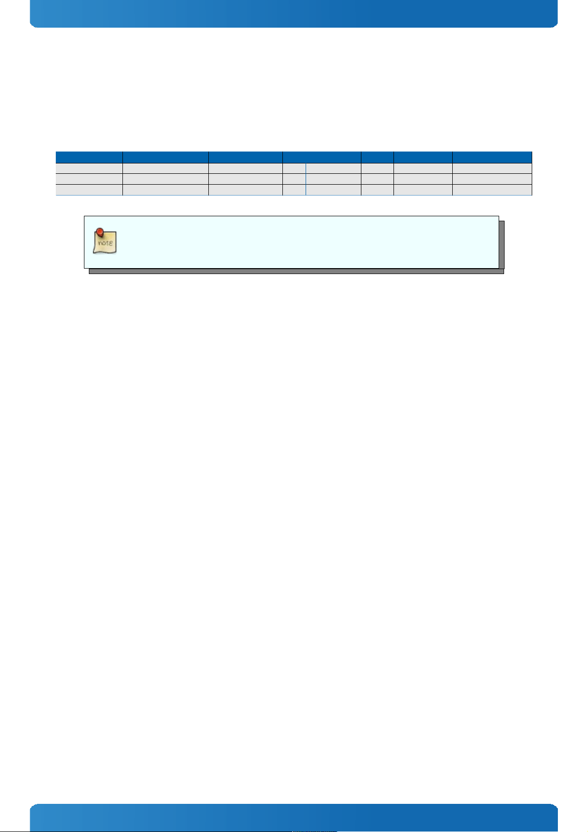
All Kontron COM Express® basic and compact modules contain two 220pin connectors; each of it has two rows called Row
A & B on primary connector and Row C & D on secondary connector. COM Express® Computer-on-modules feature the
following maximum amount of interfaces according to the PICMG module Pin-out type:
Feature Pin-Out Type 1 Pin-Out Type 10 Pin-Out Type 2 Pin-Out Type 6
HD Audio
1x 1x 1x 1x
Gbit Ethernet
1x 1x 1x 1x
Serial ATA
4x 4x 4x 4x
Parallel ATA
- - 1x -
PCI
- - 1x -
PCI Express x1
6x 6x 6x 8x
PCI Express x16 (PEG)
- - 1x 1x
USB Client
1x 1x - -
USB 2.0
8x 8x 8x 8x
USB 3.0
- 2x - 4x
VGA
1x - 1x 1x
LVDS
Dual Channel Single Channel Dual Channel Dual Channel
DP++ (SDVO/DP/HDMI/DVI)
1x optional 1x 3x shared with PEG 3x
LPC
1x 1x 1x 1x
External SMB
1x 1x 1x 1x
External I2C
1x 1x 1x 1x
GPIO
8x 8x 8x 8x
SDIO shared w/GPIO
1x optional 1x optional - 1x optional
UART (2-wire COM)
- 2x - 2x
FAN PWM out
- 1x - 1x
8
Page 9
COMe-bSC2 / Introduction
2.4 COM Express® Documentation
This product manual serves as one of three principal references for a COM Express® design. It documents the
specifications and features of COMe-bSC2. Additional references are available at your Kontron Support or at PICMG®:
» The COM Express® Specification defines the COM Express® module form factor, pin-out, and signals. This document
is available at the PICMG® website by filling out the order form.
» The COM Express® Design Guide by PICMG® serves as a general guide for baseboard design, with a focus on
maximum flexibility to accommodate a wide range of COM Express® modules.
Some of the information contained within this product manual applies only to certain
product revisions (CE: xxx). If certain information applies to specific product revisions (CE:
xxx) it will be stated. Please check the product revision of your module to see if this
information is applicable.
2.5 COM Express® Benefits
COM Express® modules are very compact, highly integrated computers. All Kontron COM Express® modules feature a
standardized form factor and a standardized connector layout which carry a specified set of signals. Each COM is based on
the COM Express® specification. This standardization allows designers to create a single-system baseboard that can
accept present and future COM Express® modules.
The baseboard designer can optimize exactly how each of these functions implements physically. Designers can place
connectors precisely where needed for the application on a baseboard designed to optimally fit a system’s packaging.
A single baseboard design can use a range of COM Express® modules with different sizes and pin-outs. This flexibility can
differentiate products at various price/performance points, or when designing future proof systems that have a built-in
upgrade path. The modularity of a COM Express® solution also ensures against obsolescence when computer technology
evolves. A properly designed COM Express® baseboard can work with several successive generations of COM Express®
modules.
A COM Express® baseboard design has many advantages of a customized computer-board design and, additionally,
delivers better obsolescence protection, heavily reduced engineering effort, and faster time to market.
9
Page 10
COMe-bSC2 / Product Specification
3 Product Specification
3.1 Module definition
The COM Express® basic sized Computer-on-Module COMe-bSC2 (CHR2 / CXR2 (HudsonBay)) follows pin-out Type 2 and is
compatible to PICMG specification COM.0 Rev 2.0. The COMe-bSC2 based on latest Huron River platform is available in
different variants to cover the demand of different performance, price and power:
Commercial grade ECC modules (0°C to 60°C operating)
Product Number Product Name Processor PCH Memory Graphics PEG TPM USB 2.0
38013-0000-21-4 COMe-bSC2 i7-2715QE ECC Intel® Core™ i7-2715QE QM67 2x DDR3-ECC HD3000 YES YES 8x
38013-0000-22-2 COMe-bSC2 i7-2655LE ECC Intel® Core™ i7-2655LE QM67 2x DDR3-ECC HD3000 YES YES 8x
38013-0000-15-2 COMe-bSC2 i7-2610UE ECC Intel® Core™ i7-2610UE QM67 2x DDR3-ECC HD3000 YES YES 8x
38013-0000-25-2 COMe-bSC2 i5-2515E ECC Intel® Core™ i5-2515E QM67 2x DDR3-ECC HD3000 YES YES 8x
38013-0000-21-2 COMe-bSC2 i3-2310E ECC Intel® Core™ i3-2310E QM67 2x DDR3-ECC HD3000 YES YES 8x
38013-0000-13-2 COMe-bSC2 i3-2340UE ECC Intel® Core™ i3-2340UE QM67 2x DDR3-ECC HD3000 YES YES 8x
38013-0000-16-1 COMe-bSC2 B810E HM65ECC Intel® Celeron® B810E HM65 2x DDR3-ECC HD YES YES CE 1.x.x: 6x
CE 2.x.x: 8x
38013-0000-11-1 COMe-bSC2 847E HM65 ECC Intel® Celeron® 847E HM65 2x DDR3-ECC HD YES YES CE 1.x.x: 6x
CE 2.x.x: 8x
38013-0000-14-0 COMe-bSC2 827E HM56 ECC Intel® Celeron® 827E HM65 2x DDR3-ECC HD YES YES CE 1.x.x: 6x
CE 2.x.x: 8x
38013-0000-10-0 COMe-bSC2 807UE HM65 ECC Intel® Celeron® 807UE HM65 1x DDR3-ECC HD - YES CE 1.x.x: 6x
CE 2.x.x: 8x
Commercial grade non-ECC modules (0°C to 60°C operating)
Product Number Product Name Processor PCH Memory Graphics PEG TPM USB 2.0
38022-0000-16-1 COMe-bSC2 B810E Intel® Celeron® B810E HM65 2x DDR3 HD YES YES 8x
38022-0000-11-1 COMe-bSC2 847E Intel® Celeron® 847E HM65 2x DDR3 HD YES YES 8x
38022-0000-14-0 COMe-bSC2 827E Intel® Celeron® 827E HM65 2x DDR3 HD YES YES 8x
38022-0000-10-0 COMe-bSC2 807UE Intel® Celeron® 807UE HM65 1x DDR3 HD - YES 8x
Extended temperature ECC modules (E1, -25°C to 75°C operating)
Product Number Product Name Processor PCH Memor y Graphics PEG TPM USB 2.0
38013-0000-22-2EXT COMe-bSC2 i7-2655LE ECC E1 Intel® Core™ i7-2655LE QM67 2x DDR3-ECC HD3000 YES - 8x
38013-0000-15-2EXT COMe-bSC2 i7-2610UE ECC E1 Intel® Core™ i7-2610UE QM67 2x DDR3-ECC HD3000 YES - 8x
38013-0000-11-1EXT COMe-bSC2 847E ECC E1 Intel® Celeron® 847E HM65 2x DDR3-ECC HD YES - CE 1.x.x: 6x
CE 2.x.x: 8x
38013-0000-14-0EXT COMe-bSC2 827E ECC E1 Intel® Celeron® 827E HM65 2x DDR3-ECC HD YES - CE 1.x.x: 6x
CE 2.x.x: 8x
38013-0000-10-0EXT COMe-bSC2 807UE ECC E1 Intel® Celeron® 807UE HM65 1x DDR3-ECC HD - - CE 1.x.x: 6x
CE 2.x.x: 8x
10
Page 11
COMe-bSC2 / Product Specification
RXT products
The RXT product line includes modules with following featureset:
» industrial (-40 to +85°C) or extended (-25 to +75°C) grade temperature range by screening
» ECC Memory support
» Kontron Rapid Shutdown support
Product Number Product Name Processor PCH Memory Graphics TPM Temperature grade
38018-0000-22-2 COMe-bSC2RXT i7-2655LE Intel® Core™ i7-2655LE QM67 2xDDR3-1333 ECC HD3000 Atmel AT97SC3204 -40 to +85°C
38018-0000-15-2 COMe-bSC2RXT i7-2610UE Intel® Core™ i7-2610UE QM67 2xDDR3-1333 ECC HD3000 Atmel AT97SC3204 -40 to +85°C
38018-0000-22-2EXT COMe-bSC2RXT i7-2655LE E1 Intel® Core™ i7-2655LE QM67 2xDDR3-1333 ECC HD3000 Atmel AT97SC3204 -25 to +75°C
Please contact your local sales for further information and MOQ for RXT modules
11
Page 12

COMe-bSC2 / Product Specification
3.2 Functional Specification
Processor
The 32nm Intel® 2nd Gen Core™ i7/i5/i3/Celeron® embedded (Sandy Bridge) CPU family with 31x24mm package size
(FCBGA1023 socket) supports:
» Intel® Turbo Boost Technology 2.0
» Intel® 64
» Intel® Virtualization Technology (VT-x)
» Intel® Virtualization Technology for Directed I/O (VT-d)
» AES New Instructions (AES-NI)
» Intel® Anti-Theft Technology
» Intel® Hyper-Threading Technology
» Enhanced Intel SpeedStep® Technology
» Idle States (C-States)
» Intel® Smart Cache
» Thermal Monitoring Technologies
» Intel® Fast Memory Access
» Intel® Flex Memory Access
» Integrated Intel® HD Graphics with Dynamic Frequency
Optional available (with customized BIOS):
» Intel® vPRO™ Technology including:
» Intel® Active Management Technology (AMT)
» Intel® Trusted Execution Technology (TXT)
The integrated Intel® HD3000 Graphics supports:
» GraphicsTechnology GT2 with 12 Execution Units
» Intel® Quick Sync Video
» Intel® InTru™ 3D Technology
» Intel® Wireless Display
» Intel® Flexible Display Interface (Intel® FDI)
» Intel® Clear Video HD Technology
» Dual Display
The integrated Intel® HD Graphics supports:
» GraphicsTechnology GT1 with 6 Execution Units
» Dual Display
12
Page 13
COMe-bSC2 / Product Specification
Intel® Core™ Core™ Core™ Core™ Core™ Core™ Celeron® Celeron® Celeron® Celeron®
- i7-2715QE i7-2655LE i7-2610UE i5-2515E i3-2310E i3-2340UE B810E 847E 827E 807UE
# of Cores 4 2 2 2 2 2 2 2 1 1
# of Threads 8 4 4 4 4 4 2 2 1 1
Clock Speed 2100MHz 2200MHz 1500MHz 2500MHz 2100MHz 1300MHz 1600MHz 1100MHz 1400MHz 1000MHz
Max Turbo Frequency 3000MHz 2900MHz 2400MHz 3100MHz - - - - - -
TDP 45W 25W 17W 35W 35W 17W 35W 17W 17W 10W
C-States C0-C7 C0-C7 C0-C7 C0-C7 C0-C7 C0-C7 C0-C3 C0-C3 C0-C3 C0-C3
Smart Cache 6MB 4MB 4MB 3MB 3MB 3MB 2MB 2MB 1.5MB 1MB
Bus/Core Ratio 12-21 8-22 8-15 8-25 8-21 8-13 8-16 8-11 8-14 8-10
Min Memory Type DDR3-1066 DDR3-1066 DDR3-1066 DDR3-1066 DDR3-1066 DDR3-1066 DDR3-1066 DDR3-1066 DDR3-1066 DDR3-1066
Max Memory Type DDR3-1600 DDR3-1333 DDR3-1333 DDR3-1333 DDR3-1333 DDR3-1333 DDR3-1333 DDR3-1333 DDR3-1333 DDR3-1333
Max Memory Size 16GB 16GB 16GB 16GB 16GB 16GB 16GB 16GB 16GB 4GB
# of Memory Channels 2 2 2 2 2 2 2 2 2 1
Graphics Model HD3000 HD3000 HD3000 HD3000 HD3000 HD3000 HD HD HD HD
GFX Base Frequency 650MHz 650MHz 350MHz 650MHz 650MHz 350MHz 650MHz 350MHz 350MHz 350MHz
GFX Max Dynamic Frequ. 1200MHz 1000MHz 850MHz 1100MHz 1050MHz 800MHz 1000MHz 800MHz 800MHz 800MHz
Quick Sync Video Yes Yes Yes Yes Yes Yes - - - -
InTru™ 3D Yes Yes Yes Yes Yes Yes - - - -
Wireless Display Yes Yes Yes Yes Yes Yes - - - -
Clear Video HD Yes Yes Yes Yes Yes Yes - - - -
PCI Express Graphics Yes Yes Yes Yes Yes Yes Yes Yes Yes -
vPRO™ (optional) Yes Yes Yes Yes - - - - - -
TXT (optional) Yes Yes Yes Yes - - - - - -
AES-NI Yes Yes Yes Yes - - - - - -
VT-x Yes Yes Yes Yes Yes Yes Yes Yes Yes Yes
VT-d Yes Yes Yes Yes - - - - - -
Anti-Theft Yes Yes Yes Yes Yes Yes - - - -
The Bus/Core Ratio shows the possible CPU Performance settings (CPU Ratio) from the max
Efficiency Ratio (LFM = Lowest Frequency Mode) to the maximum non-turbo Ratio (HFM =
Highest Frequency Mode). If enabled in Setup, CPU Clock is fixed to Ratio*100MHz. This
feature is not supported with updated EFI Core available with BIOS CHR2R111 or newer.
Memory
Sockets
2x DDR3 SO-DIMM
Memory Type
DDR3-1066/1333 ECC/nonECC
Maximum Size
2x8GB
Technology
Dual Channel
Chipset
The Intel® 6-Series Platform Controller Hub Cougar Point supports:
» PCI Express Revision 2.0
» PCI Express Configurations x1, x2, x4
» Intel® Virtualization Technology for Directed I/O (VT-d)
» Intel® Trusted Execution Technology (TXT)
» Intel® vPro Technology
» Intel® Active Management Technology 7.0
» Intel® Anti-Theft Technology
» Intel® Rapid Storage Technology
13
Page 14
COMe-bSC2 / Product Specification
PCH comparison
Feature QM67 HM65
TDP 3.9W 3.9W
VT-d YES NO
TXT YES NO
vPRO YES NO
AMT YES NO
Rapid Storage YES NO
SATA RAID YES NO
The Intel® vPro Technology including Trusted Execution Technology (TXT) and Active
Management Technology (AMT) is not supported by default on COMe-bSC2. Please contact
your local sales or support for custom BIOS variants supporting vPro. A test version is
available on EMD Customer Section.
Graphics Core
The integrated Intel® GMA HD/HD3000 (Gen6) supports:
Graphics Core Render Clock
GT1 /GT2, Base clock: 350/650 MHz, GT Turbo: up to 1200 MHz
Execution Units / Pixel Pipelines
GT2: 12EU / GT1: 6EU
Max Graphics Memory
1720MB
GFX Memory Bandwidth (GB/s)
21.3
GFX Memory Technology
DVMT 5.0
API (DirectX/OpenGL)
10.1 / 3.1
Shader Model
4.0
Hardware accelerated Video
MPEG2, VC-1, AVC, Blu-ray (+3D)
Independent/Simultaneous Displays
2
Display Port
DP 1.1a / eDP
HDCP support
HDCP 1.4
Monitor output
CRT max Resolution
2048x1536
TV out:
-
LVDS
LVDS Bits/Pixel
1x18/24, 2x18/24
LVDS Bits/Pixel with dithering
-
LVDS max Resolution:
1920x1200
PWM Backlight Control:
YES
Supported Panel Data:
JILI2/JILI3/EDID/DID
Display Interfaces
Discrete Graphics
1x PEG 2.0 (not on Cel. 807UE)
Digital Display Interface DDI1
DP++/SDVOB
Digital Display Interface DDI2
DP++
Digital Display Interface DDI3
DP++/eDP
Maximum Resolution on DDI
2560x1600
14
Page 15
COMe-bSC2 / Product Specification
PEG Configuration
The x16 PCI Express Graphics Port (PEG) is compatible to standard PCI Express devices like Ethernet or RAID controllers.
The COMe-bSC2 supports following PEG Port configuration when used as PCI Express Interface:
» 1×16
» 1×8
» 1×4
» 1×2
» 1×1
The internal PCI Express controller can be re-configured to support up to 3 PCIe ports. The following port configurations
are available via hardware strap options (customized article):
» 2×8 (lanes #0-7 + #8-15)
» 1×8 + 2×4 (lanes #0-7 + #8-11 + #12-15)
Storage
onboard SSD
-
SD Card support
-
IDE Interface
JMB368 PCIe2PATA
Serial-ATA
2x SATA 6Gb/s, 2x SATA 3Gb/s
SATA AHCI
NCQ, HotPlug, Staggered Spinup, eSATA, PortMultiplier
SATA RAID
0, 1, 5, 10, MATRIX (QM67 only)
If SATA AHCI or RAID is disabled in setup, the SATA Interface only supports 3Gb/s transfer
rate and Staggered Spin-Up. To configure a RAID enable RAID support in BIOS Chipset/SATA
settings, connect at least two hard drives and enter the RAID Option ROM by pressing
'CTRL'+'I'
Connectivity
USB 2.0
up to 8x USB 2.0
USB 3.0
-
USB Client
-
PCI
PEX8112 PCIe2PCI
PCI External Masters
4
PCI Express
5x PCIe x1 Gen2
Max PCI Express
6x PCIe without PCIe2PATA Bridge
PCI Express x2/x4 configuration
YES (Softstrap option)
Ethernet
10/100/1000 Mbit
Ethernet controller
Intel® 82579LM (Lewisville)
15
Page 16
COMe-bSC2 / Product Specification
PCI Express Configuration
The COMe-bSC2 only supports x1 PCIexpress lane configuration by default. Following x2/x4 configurations are possible
via Management Engine Softstrap Options:
PCIe Port #0 Port #1 Port #2 Port #3 Port #4 Port #5* Port #6* Port #7*
Configuration0 x1 x1 x1 x1 x1 - - -
Configuration1 x2 x1 x1 x1 x1 x1 x1
Configuration2 x2 x2 x1 x1 x1 x1
Configuration3 x2 x2 x2 x1 x1
Configuration4 x2 x2 x2 x2
Configuration5 x4 x1 x1 x1 x1
Configuration6 x4 x2 x1 x1
Configuration7 x4 x2 x2
Configuration8 x4 x4
- *PCIe Ports #5 to #7 are only available without PCIe2PATA Bridge, PCIe2PCI Bridge and
without Ethernet Controller
- Configuration0 (default) and Configuration5 (modified FlashDescriptor) are provided in
BIOS download package available on EMD Customer Section
Ethernet
The Intel® 82579LM (Lewisville) ethernet supports:
» Jumbo Frames
» MACsec IEEE 802.1 AE
» Time Sync Protocol Indicator
» WOL (Wake On LAN)
» PXE (Preboot eXecution Environment)
Misc Interfaces and Features
Supported BIOS Size/Type
8MB SPI
Audio
HD Audio + DisplayPort dual stream
Onboard Hardware Monitor
Analog Devices ADT7490
Trusted Platform Module
Atmel AT97SC3204
Miscellaneous
-
Kontron Features
External I2C Bus
Fast I2C, MultiMaster capable
M.A.R.S. support
YES
Embedded API
KEAPI1 / KEAPI2
Custom BIOS Settings / Flash Backup
YES
Watchdog support
Dual Staged
Additional features
» All solid capacitors (POSCAP). No tantalum capacitors used.
» Optimized RTC Battery monitoring to secure highest longevity
» Real fast I2C with transfer rates up to 40kB/s.
» Discharge logic on all onboard voltages for highest reliability
16
Page 17
COMe-bSC2 / Product Specification
Power Features
Singly Supply Support
YES
Supply Voltage
8.5V - 18V (20V@nonECC)
ACPI
ACPI 4.0
S-States
S0, S3, S4, S5
S5 Eco Mode
YES
Misc Power Management
DPST 6.0, Rapid Shutdown @ RXT Ver.
Power Consumption and Performance
Full Load Power Consumption
10 - 73W
Kontron Performance Index
11571 - 63719
Kontron Performance/Watt
878 - 1612
*Measured Values. Please note the maximum Power Consumption with activated Turbo Mode in chapter Turbo 2.0
Detailed Power Consumption measurements in all states and benchmarks for CPU, Graphics
and Memory performance are available in Application Note KEMAP054 at EMD Customer
Section.
17
Page 18
COMe-bSC2 / Product Specification
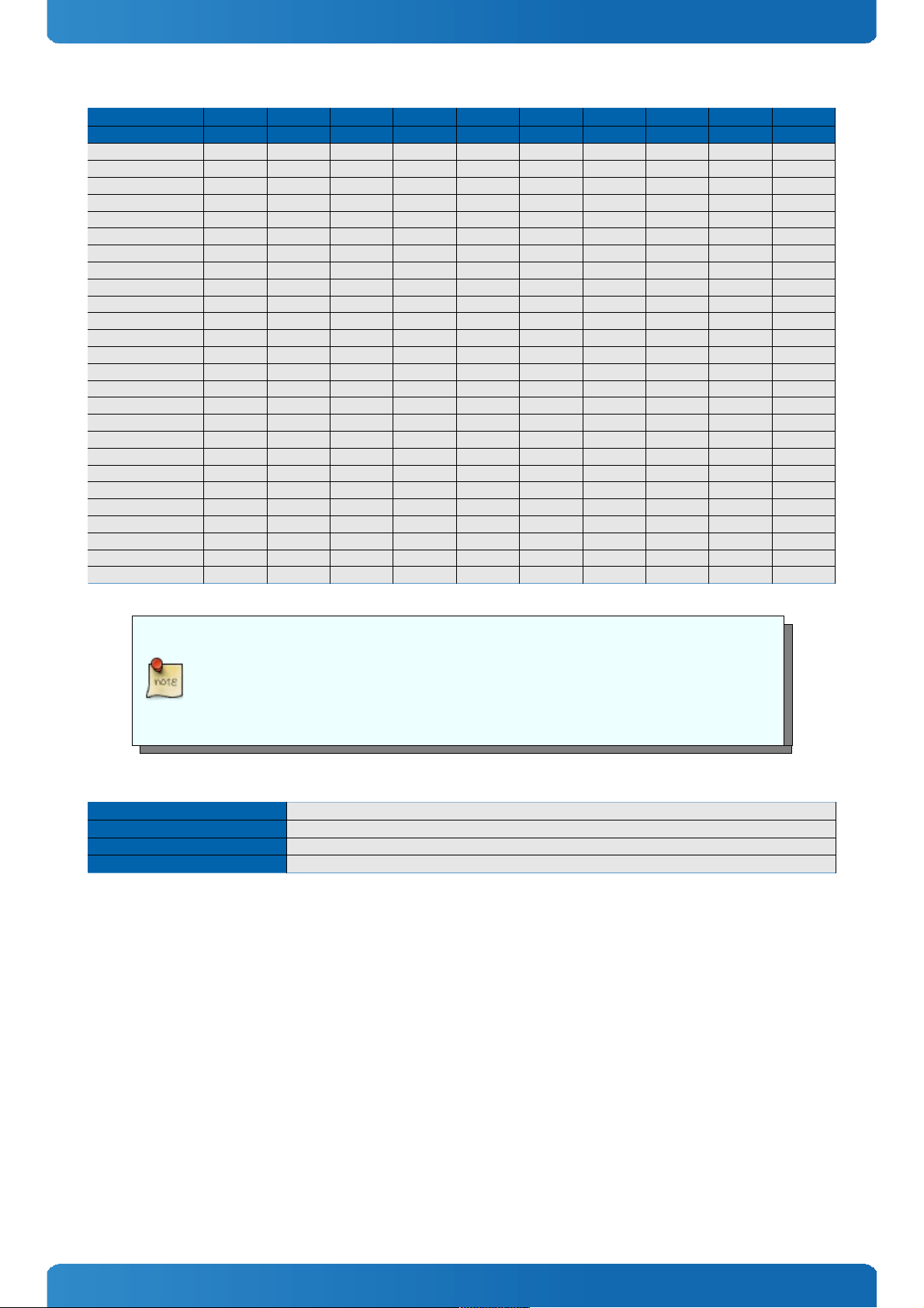
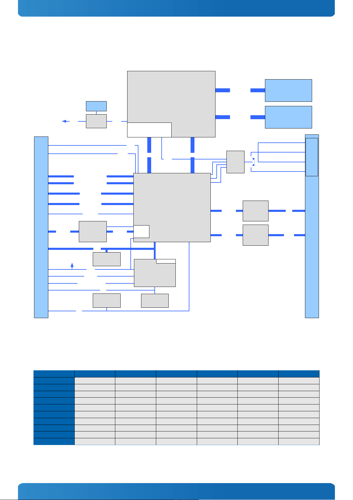
3.3 Block Diagram
3.4 Variant Matrix
The COMe-bSC2 is available in several configurations. The following table shows major differences of available standard
modules:
Product Name COMe-bSC2 ECC COMe-bSC2 ECC COMe-bSC2 ECC E1 COMe-bSC2 ECC E1 COMe-bSC2RXT ECC COMe-bSC2
Part.No.
38013-xxxx-xx-x 38013-xxxx-xx-x 38013-xxxx-xx-xEXT 38013-xxxx-xx-xEXT 38018-xxxx-xx-x 38022-xxxx-xx-x
Temperature Grade
commercial commercial extended extended industrial commercial
PCB/Project Code
CHR2 CHR2 CHR2 CHR2 Hudson Bay CCR2
BIOS/UEFI
CHR2Rxxx CHR2Rxxx CHR2Rxxx CHR2Rxxx CHR2Rxxx CHR2Rxxx
HW Revision
CE 1.x.x CE 2.x.x CE 1.x.x CE 2.x.x All All
DDR3 Memory
ECC ECC ECC ECC ECC non-ECC
USB #6/#7 Support
with QM67 PCH only Yes with QM67 PCH only Yes Yes Yes
eDP Support on DDI3
No Yes No Yes No Yes
TPM
Infineon FW 1.02 Infineon FW 3.17 No No Atmel AT97SC3204 Infineon FW 3.17
onboard HWM
ADT7490 ADT7490 ADT7490 ADT7490 ADT7490 NCT7802Y
18
PATA
PCI
PEG
PwrCtrl / Battery
DDR3-1333
DDR3-1333
X4 DMIFDI
PCIe #0 - #4
Intel® 2nd Generation Core
GMA HD3000
SATA #0/1 (6Gb/s)
HDAudio
I2C
Connector CD
USB #0 - #7
PCIe #7GB LAN
CPLD
(Embedded
Controller)
JIDA
EEPROM
8 GPIO
FAN
Connector
SPI
SMB
DDR3 SODIMM
(ECC or nonECC)
DDR3 SODIMM
(ECC or nonECC)
CRT
LVDS
DDI1
DDI2
DDI3
PEG
SDVO/DP/HDMI/DVI
DP/HDMI/DVI
eDP/DP/HDMI/DVI
PEG
SATA #2/3 (3Gb/s)
PCIe2PCI
PEX8112
PCIe #6
Ethernet
Intel® 82579
PCIe2PATA
JMB368
PCIe #5
Watchdo g
HWM
ADT7490
PECISMB
HWM
LPC
TPM
Infineon
SLB9635TT
Connector AB
BIOS
SPI Flash
Intel® 6-Series PCH
Intel® QM67
Intel® HM65
Ethernet
MAC
PCIe
signal
switch
DDIB
DDIC
DDID
Page 19
COMe-bSC2 / Product Specification
3.5 Accessories
Product specific accessories
Product Number Heatspreader and Cooling Solutions Comment
38013-0000-99-0 HSP COMe-bSC/IP thread For CPUs up to 25W TDP and commercial temperature grade usage
38013-0000-99-1 HSP COMe-bSC/IP through For CPUs up to 25W TDP and commercial temperature grade usage
38013-0000-99-2 HSP COMe-bSC/IP heatpipe thread For all CPUs and temperature grades
38013-0000-99-3 HSP COMe-bSC/IP heatpipe through For all CPUs and temperature grades
38013-0000-99-0C05 HSK COMe-bSC/IP active setscrew thread For all CPUs and commercial temperature grade usage
38013-0000-99-1C05 HSK COMe-bSC/IP active setscrew through hole For all CPUs and commercial temperature grade usage
38013-0000-99-0C06 HSK COMe-bSC/IP passive setscrew thread For all CPUs and commercial temperature grade usage
38013-0000-99-1C06 HSK COMe-bSC/IP passive setscrew through hole For all CPUs and commercial temperature grade usage
General accessories
Part Number COMe pin-out Type 2 compatible accessories Project Code Comment
38102-0000-00-1 COM Express® Reference Carrier Type 2 ADAE mITX Carrier with 8mm COMe connector
38104-0000-00-0 COM Express® Eval Carrier Type 2 Niles Canyon ATX Carrier with 5mm COMe connector (EOL)
38104-0000-00-1 COM Express® Eval Carrier Type 2 Topanga Canyon ATX Carrier with 5mm COMe connector
96006-0000-00-7 ADA-Type2-DP3 DVOD (sandwich) Adapter Card for 3x DisplayPort
38019-0000-00-0 ADA-COMe-Height-dual EERC Height Adapter
36100-0000-00-S COMe Ref. Starterkit T2 ADAE Starterkit with COMe Reference Carrier T2
Part Number Mounting Comment
38017-0000-00-5 COMe Mount KIT 5mm 1set Mounting Kit for 1 module including screws for 5mm connectors
38017-0100-00-5 COMe Mount KIT 5mm 100sets Mounting Kit for 100 modules including screws for 5mm connectors
38017-0000-00-0 COMe Mount KIT 8mm 1set Mounting Kit for 1 module including screws for 8mm connectors
38017-0100-00-0 COMe Mount Kit 8mm 100sets Mounting Kit for 100 modules including screws for 8mm connectors
Part Number Display Adapter Comment
9-5000-0352 ADA-LVDS-DVI 18bit LVDS to DVI converter
9-5000-0353 ADA-LVDS-DVI 24bit LVDS to DVI converter
96006-0000-00-8 ADA-DP-LVDS DP to LVDS adapter
96082-0000-00-0 KAB-ADAPT-DP-DVI DP to DVI adapter cable
96083-0000-00-0 KAB-ADAPT-DP-VGA DP to VGA adapter cable
96084-0000-00-0 KAB-ADAPT-DP-HDMI DP to HDMI adapter cable
Part Number Cables Comment
96079-0000-00-0 KAB-HSP 200mm Cable adapter to connect FAN to module (COMe basic/compact)
96079-0000-00-2 KAB-HSP 40mm Cable adapter to connect FAN to module (COMe basic/compact)
Part Number Miscellaneous Comment
18029-0000-00-0 MARS Smart Battery Kit Starterkit Kontron Mobile Application platform for Rechargeable Systems
For COMe-bSC2 ECC (38013-xxxx-xx-x) & COMe-bSC2RXT (38018-xxxx-xx-x)
Part Number DDR3 ECC SODIMM, commercial temperature grade
97016-1024-16-0 DDR3-1600 SODIMM 1GB ECC
97016-2048-16-0 DDR3-1600 SODIMM 2GB ECC
97016-4096-16-0 DDR3-1600 SODIMM 4GB ECC
97016-8192-16-0 DDR3-1600 SODIMM 8GB ECC
Part Number DDR3 ECC SODIMM, industrial temperature grade
97016-1024-16-2 DDR3-1600 SODIMM 1GB ECC E2
97016-2048-16-2 DDR3-1600 SODIMM 2GB ECC E2
97016-4096-16-2 DDR3-1600 SODIMM 4GB ECC E2
97016-8192-16-2 DDR3-1600 SODIMM 8GB ECC E2
For COMe-bSC2 non-ECC (38022-xxxx-xx-x)
Part Number DDR3 SODIMM, commercial temperature grade
97015-1024-16-0 DDR3-1600 SODIMM 1GB
97015-2048-16-0 DDR3-1600 SODIMM 2GB
97015-4096-16-0 DDR3-1600 SODIMM 4GB
97015-8192-16-0 DDR3-1600 SODIMM 8GB
Part Number DDR3 SODIMM, industrial temperature grade
97015-1024-16-2 DDR3-1600 SODIMM 1GB E2
97015-2048-16-2 DDR3-1600 SODIMM 2GB E2
97015-4096-16-2 DDR3-1600 SODIMM 4GB E2
97015-8192-16-2 DDR3-1600 SODIMM 8GB E2
19
Page 20

COMe-bSC2 / Product Specification
3.6 Electrical Specification
3.6.1 Supply Voltage
Following supply voltage is specified at the COM Express® connector:
VCC:
8.5V - 18V (20V@nonECC)
Standby:
5V DC +/- 5%
RTC:
2.5V - 3.47V
- 5V Standby voltage is not mandatory for operation.
- Extended Temperature (E1) variants are validated for 12V supply only
3.6.2 Power Supply Rise Time
» The input voltages shall rise from ≤10% of nominal to within the regulation ranges within 0.1ms to 20ms.
» There must be a smooth and continuous ramp of each DC input voltage from 10% to 90% of its final set-point
following the ATX specification
3.6.3 Supply Voltage Ripple
» Maximum 100 mV peak to peak 0 – 20 MHz
3.6.4 Power Consumption
The maximum Power Consumption of the different COMe-bSC2 variants is 10 - 73W (100% CPU load on all cores; 90°C CPU
temperature). Further information with detailed measurements are available in Application Note KEMAP054 available on
EMD Customer Section. Information there is available after registration.
20
Page 21
COMe-bSC2 / Product Specification
3.6.5 ATX Mode
By connecting an ATX power supply with VCC and 5VSB, PWR_OK is set to low level and VCC is off. Press the Power Button to
enable the ATX PSU setting PWR_OK to high level and powering on VCC. The ATX PSU is controlled by the PS_ON# signal
which is generated by SUS_S3# via inversion. VCC can be 8.5V - 18V (20V@nonECC) in ATX Mode. On Computer-onModules supporting a wide range input down to 4.75V the input voltage shall always be higher than 5V Standby (VCC >
5VSB).
State PWRBTN# PWR_OK V5_StdBy PS_ON# VCC
G3 x x 0V x 0V
S5 high low 5V high 0V
S5 S0 → PWRBTN Event low high → 5V high low → 0 V VCC →
S0 high high 5V low VCC
3.6.6 Single Supply Mode
In single supply mode (or automatic power on after power loss) without 5V Standby the module will start automatically
when VCC power is connected and Power Good input is open or at high level (internal PU to 3.3V). PS_ON# is not used in
this mode and VCC can be 8.5V - 18V (20V@nonECC).
To power on the module from S5 state press the power button or reconnect VCC. Suspend/Standby States are not
supported in Single Supply Mode.
State PWRBTN# PWR_OK V5_StdBy VCC
G3 x x x 0
G3 S0 → high open / high x connecting VCC
S5 high open / high x VCC
S5 S0 → PWRBTN Event open / high x reconnecting VCC
Signals marked with “x” are not important for the specific power state. There is no
difference if connected or open.
All ground pins have to be tied to the ground plane of the carrier board.
21
Page 22
COMe-bSC2 / Product Specification
3.7 Power Control
Power Supply
The COMe-bSC2 supports a power input from 8.5V - 18V (20V@nonECC). The supply voltage is applied through the VCC pins
(VCC) of the module connector.
Power Button (PWRBTN#)
The power button (Pin B12) is available through the module connector described in the pinout list. To start the module via
Power Button the PWRBTN# signal must be at least 50ms (50ms ≤ t < 4s, typical 400ms) at low level (Power Button Event).
Pressing the power button for at least 4seconds will turn off power to the module (Power Button Override).
Power Good (PWR_OK)
The COMe-bSC2 provides an external input for a power-good signal (Pin B24). The implementation of this subsystem
complies with the COM Express® Specification. PWR_OK is internally pulled up to 3.3V and must be high level to power on
the module.
Reset Button (SYS_RESET#)
The reset button (Pin B49) is available through the module connector described in the pinout list. The module will stay in
reset as long as SYS_RESET# is grounded. If available, the BIOS setting for “Reset Behavior” must be set to “Power Cycle”.
Modules with Intel® Chipset and active Management Engine do not allow to hold the
module in Reset out of S0 for a long time. At about 10s holding the reset button the ME will
reboot the module automatically
SM-Bus Alert (SMB_ALERT#)
With an external battery manager present and SMB_ALERT# (Pin B15) connected the module always powers on even if
BIOS switch “After Power Fail” is set to “Stay Off”.
22
Page 23
COMe-bSC2 / Product Specification
3.8 Environmental Specification
3.8.1 Temperature Specification
Kontron defines following temperature grades for Computer-on-Modules in general. Please see chapter 'Product
Specification' for available temperature grades for the COMe-bSC2
Temperature Specification Operating Non-operating Validated Input Voltage
Commercial grade 0°C to +60°C -30°C to +85°C VCC: 8.5V - 18V (20V@nonECC)
Extended Temperature (E1) -25°C to +75°C -30°C to +85°C VCC: 12V
Industrial grade by Screening (XT)
-40°C to +85°C -40°C to +85°C VCC: 12V
Industrial grade by Design (E2)
-40°C to +85°C -40°C to +85°C VCC: 8.5V - 18V (20V@nonECC)
Operating with Kontron heatspreader plate assembly
The operating temperature defines two requirements:
» the maximum ambient temperature with ambient being the air surrounding the module.
» the maximum measurable temperature on any spot on the heatspreader's surface
Test specification:
Temperature Grade Validation requirements
Commercial grade at 60°C HSP temperature the CPU @ 100% load needs to run at nominal frequency
Extended Temperature (E1) at 75°C HSP temperature the CPU @ 75% load is allowed to start speedstepping for thermal protection
Industrial grade by Screening (XT)
at 85°C HSP temperature the CPU @ 50% load is allowed to start throttling for thermal protection
Industrial grade by Design (E2)
at 85°C HSP temperature the CPU @ 50% load is allowed to start throttling for thermal protection
Operating without Kontron heatspreader plate assembly
The operating temperature is the maximum measurable temperature on any spot on the module's surface.
3.8.2 Humidity
» 93% relative Humidity at 40°C, non-condensing (according to IEC 60068-2-78)
23
Page 24
COMe-bSC2 / Product Specification
3.9 Standards and Certifications
RoHS II
The COMe-bSC2 is compliant to the directive 2011/65/EU on the Restriction of the use of certain Hazardous Substances
(RoHS II) in electrical and electronic equipment
Component Recognition UL 60950-1
The COM Express® basic form factor Computer-on-Modules are Recognized by Underwriters Laboratories Inc.
Representative samples of this component have been evaluated by UL and meet applicable UL requirements.
UL Listings:
» NWGQ2.E304278
» NWGQ8.E304278
WEEE Directive
WEEE Directive 2002/96/EC is not applicable for Computer-on-Modules.
Conformal Coating
Conformal Coating is available for Kontron Computer-on-Modules and for validated SO-DIMM memory modules. Please
contact your local sales or support for further details.
24
Page 25

COMe-bSC2 / Product Specification
Shock & Vibration
The COM Express® basic form factor Computer-on-Modules successfully passed shock and vibration tests according to
» IEC/EN 60068-2-6 (Non operating Vibration, sinusoidal, 10Hz-4000Hz, +/-0.15mm, 2g)
» IEC/EN 60068-2-27 (Non operating Shock Test, half-sinusoidal, 11ms, 15g)
EMC
Validated in Kontron reference housing for EMC the COMe-bSC2 follows the requirements for electromagnetic
compatibility standards
» EN55022
25
Page 26
COMe-bSC2 / Product Specification
3.10 MTBF
The following MTBF (Mean Time Before Failure) values were calculated using a combination of manufacturer’s test data, if
the data was available, and the Telcordia (Bellcore) issue 2 calculation for the remaining parts.
The calculation method used is “Telcordia Issue 2 Method 1 Case 3” in a ground benign, controlled environment (GB,GC).
This particular method takes into account varying temperature and stress data and the system is assumed to have not
been burned in.
Other environmental stresses (extreme altitude, vibration, salt water exposure, etc) lower MTBF values.
System MTBF (hours): 222498 @ 40°C (w/PCB)
Fans usually shipped with Kontron Europe GmbH products have 50,000-hour typical
operating life. The above estimates assume no fan, but a passive heat sinking arrangement
Estimated RTC battery life (as opposed to battery failures) is not accounted for in the above
figures and need to be considered separately. Battery life depends on both temperature
and operating conditions. When the Kontron unit has external power; the only battery
drain is from leakage paths.
26
Page 27
COMe-bSC2 / Product Specification
3.11 Mechanical Specification
Dimension
» 95.0 mm x 125.0 mm
» Height approx. 12mm (0.4”)
CAD drawings are available at EMD CustomerSection
Height
The COM Express® specification defines a module height of 13mm from module PCB bottom to heatspreader top:
Cooling solutions provided from Kontron Europe GmbH for basic sized Computer-on-Modules are 27mm in height from
module bottom to Heatsink top.
Universal Cooling solutions to be mounted on the HSP (36099-0000-00-x) are 14.3mm in height for an overall height of
27.3mm from module bottom to Heatsink top.
27
Page 28
COMe-bSC2 / Product Specification
3.12 Module Dimensions
28
Page 29

COMe-bSC2 / Product Specification
3.13 Thermal Management, Heatspreader and Cooling Solutions
A heatspreader plate assembly is available from Kontron Europe GmbH for the COMe-bSC2. The heatspreader plate on top
of this assembly is NOT a heat sink. It works as a COM Express®-standard thermal interface to use with a heat sink or
external cooling devices.
External cooling must be provided to maintain the heatspreader plate at proper operating temperatures. Under worstcase conditions, the cooling mechanism must maintain an ambient air and heatspreader plate temperature on any spot of
the heatspreader's surface according the module specifications:
» 60°C for commercial grade modules
» 75°C for extended temperature grade modules (E1)
» 85°C for industrial temperature grade modules (E2/XT)
The aluminum slugs and thermal pads or the heat-pipe on the underside of the heatspreader assembly implement thermal
interfaces between the heatspreader plate and the major heat-generating components on the COMe-bSC2. About 80
percent of the power dissipated within the module is conducted to the heatspreader plate and can be removed by the
cooling solution.
You can use many thermal-management solutions with the heatspreader plates, including active and passive approaches.
The optimum cooling solution varies, depending on the COM Express® application and environmental conditions. Active
or passive cooling solutions provided from Kontron Europe GmbH for the COMe-bSC2 are usually designed to cover the
power and thermal dissipation for a commercial grade temperature range used in a housing with proper air flow.
Documentation and CAD drawings of COMe-bSC2 heatspreader and cooling solutions are provided at
http://emdcustomersection.kontron.com.
29
Page 30
COMe-bSC2 / Product Specification
3.14 Onboard Fan Connector
Location of the FAN Connector
Specification of the FAN Connector:
» Part number (Molex) J8: 53261-0371
» Mates with: 51021-0300
» Crimp terminals: 50079-8100
Pin assignment
» Pin1: Tacho, Pin2: VCC, Pin3: GND
Electrical characteristic
Module Input Voltage 8.5 - 13V 13 - 18V
FAN Output Voltage
8.5 - 13V 13V
Max. FAN Output Current
350mA 200mA
To connect a standard FAN with 3pin connector to the module please use adaptor cable
KAB-HSP 200mm (96079-0000-00-0) or KAB-HSP 40mm (96079-0000-00-2)
30
Page 31

COMe-bSC2 / Features and Interfaces
4 Features and Interfaces
4.1 S5 Eco Mode
Kontron’s new high-efficient power-off state S5 Eco enables lowest power-consumption in soft-off state – less than 1 mA
compared to the regular S5 state this means a reduction by at least factor 200!
In the “normal” S5 mode the board is supplied by 5V_Stb and needs usually up to 300mA just to stay off. This mode allows
to be switched on by power button, RTC event and WakeOnLan, even when it is not necessary. The new S5 Eco mode
reduces the current enormous.
The S5 Eco Mode can be enabled in BIOS Setup, when the BIOS supports this feature.
Following prerequisites and consequences occur when S5 Eco Mode is enabled
» The power button must be pressed at least for 200ms to switch on.
» Wake via Power button only.
» “Power On After Power Fail”/“State after G3”: only “stay off” is possible
31
Page 32

COMe-bSC2 / Features and Interfaces
4.2 Rapid Shutdown
Overview
For “R” or the “RXT” version of the COMe-bSC2, Kontron has implemented a rapid shutdown function. It works as follows:
1) An active-high shutdown signal is asserted by the COM Express Eval Type 2 carrier board via pin C67 of the COM Express
connector. The characteristics of the shutdown signal are as follows:
» Amplitude 5.0V +/- 5%
» Source impedance < = 50 ohms
» Rise time 1uS⇐
» Duration >= 20uS
The assertion of this signal causes all power regulators to be disabled and the internal power supply rails to be discharged
by crowbar circuits. The shutdown circuitry provides internal energy storage that maintains crowbar activation for at least
2mS following the de-assertion of the shutdown signal. The circuit also incorporates a weak input pulldown resistor so
that the RXT module will operate normally in systems where the rapid shutdown functionality is not used and pin C67 of
the COM Express is left unconnected.
2) Simultaneously with the leading edge of shutdown, the 12V (main) input power to the RXT module is removed and
these input power pins are externally clamped to ground though a crowbar circuit located on the COM Express carrier
board. This external clamping circuit must maintain a maximum resistance of approximately 1 ohm and be activated for a
minimum of 2mS.
3) Simultaneously with the leading edge of shutdown, the 5V (standby) input power to the RXT module is removed, if
present. External clamping on these pins is not necessary.
Crowbar implementation details
As a tool for designing the internal crowbars, Kontron developed tallied the total capacitance present on each of the
internal power rails, and calculates the required discharge resistance in order to achieve the desired voltage decay time
constant. The principal design criteria are that each supply rail must decay to 37% of initial value (equivalent to 1RC)
within 250uS, and to below 1.5V within 2mS. Analysis shows that the power rails fall into four general classes. Each class
of power rails has a corresponding discharge strategy.
1) Power Input Rails: The main 12V power input rail incorporates about 300uF of distributed capacitance. This rail must be
discharged by an external crowbar located on the carrier board, which must provide a shunt resistance of approximately 1
ohm. The peak power dissipation in this crowbar resistance will be relatively high (on the order of 150W when the crowbar
is activated), but will diminish very rapidly as the input capacitors discharge.
2) Low Voltage, High Power Rails: Each of these 5 “major” internal supply rails has an output voltage in the 1.0 V to 1.5V
range, and each rail has between 1500uF and 3300uF of output capacitance. The required discharge resistances for these
rails are in the range of 0.1 to 0.2 ohm, and peak discharge currents are in the range of 8 to 16A.
The discharge circuit for each rail is implemented with a “pulse withstanding” thick-film SMT resistor in series with a lowRDSon MOSFET. The resistor peak powers are in the 8W to 20W range; depending on PCB layout considerations either a
single resistor or multiple smaller resistors may be used to achieve sufficient pulse handling capability.
Because of the relatively high currents in the discharge paths, these crowbar circuits require wide copper traces and
careful component placement adjacent to the output components of the corresponding power supplies.
3) Low Voltage, Low Power Rails: These rails have voltages of 1.8V or less and capacitances under 1000uF, with peak
discharge currents <3A. The discharge circuits for these rails are also implemented with resistor(s) and a low-RDSon
32
Page 33

COMe-bSC2 / Features and Interfaces
MOSFET. In some cases, the peak pulse power dissipation in the resistor(s) is low enough that specialty “pulse
withstanding” resistors are not required.
4) Medium Voltage Rails: These 3.3V and 5V rails typically have relatively small output capacitances and peak discharge
currents <1A. The discharge circuits for these rails are typically implemented with conventional resistor(s) and a lowRDSon MOSFET.
Shutdown input circuit details
The shutdown input pin to the RXT module is coupled through a series Schottky diode and a small series resistor to the
gates of all crowbar MOSFETs, connected in parallel. All crowbar MOSFETs are N-channel “logic level” parts that have are
specified for operation at Vgs = 4.5V. Three additional components are connected in parallel between the MOSFET gates
and ground:
» A capacitor that provides energy storage to keep the MOSFETs conducting for several mS after the shutdown signal
is de-asserted.
» A high-value resistor that provides a discharge path for the capacitor as well as a pulldown resistance (to insure
that the shutdown circuits remain inactive if the shutdown pin is left floating).
» A 6.2V zener diode that protects the MOSFET gates from damage due to input ESD or input overdrive.
In order to insure that the crowbars do not “fight” active switching regulators while the input capacitors are being
discharged, the shutdown circuit rapidly crowbars the 5V rail, with a time constant <10uS. The 5V rail powers most of the
remaining switching regulators, and as its voltage falls below about 4V those regulators enter under-voltage lockout
mode and cease to operate. Additionally, by using the UVLO mechanism in the design of the RXT module, Kontron
minimizes the risk of inadvertently affecting the standard power sequencing logic for such RXT modules. Two of the
switching regulators do not require the 5V supply for operation, and in those two cases it will be necessary to clamp the
enable inputs to ground when shutdown begins.
33
Page 34

COMe-bSC2 / Features and Interfaces
4.3 LPC
The Low Pin Count (LPC) Interface signals are connected to the LPC Bus bridge located in the CPU or chipset. The LPC low
speed interface can be used for peripheral circuits such as an external Super I/O Controller, which typically combines
legacy-device support into a single IC. The implementation of this subsystem complies with the COM Express®
Specification. Implementation information is provided in the COM Express® Design Guide maintained by PICMG. Please
refer to the official PICMG documentation for additional information.
The LPC bus does not support DMA (Direct Memory Access) and a clock buffer is required when more than one device is
used on LPC. This leads to limitations for ISA bus and SIO (standard I/O´s like Floppy or LPT interfaces) implementations.
All Kontron COM Express® Computer-on-Modules imply BIOS support for following external baseboard LPC Super I/O
controller features for the Winbond/Nuvoton 5V 83627HF/G and 3.3V 83627DHG-P:
83627HF/G Phoenix BIOS AMI CORE8 AMI / Phoenix EFI
PS/2 YES YES YES
COM1/COM2 YES YES YES
LPT YES YES YES
HWM YES YES NO
Floppy NO NO NO
GPIO NO NO NO
83627DHG-P Phoenix BIOS AMI CORE8 AMI / Phoenix EFI
PS/2 YES YES YES
COM1/COM2 YES YES YES
LPT YES YES YES
HWM NO NO NO
Floppy NO NO NO
GPIO NO NO NO
Features marked as not supported do not exclude OS support (e.g. HWM can be accessed via SMB). For any other LPC
Super I/O additional BIOS implementations are necessary. Please contact your local sales or support for further details.
34
Page 35

COMe-bSC2 / Features and Interfaces
4.4 Serial Peripheral Interface (SPI)
The Serial Peripheral Interface Bus or SPI bus is a synchronous serial data link standard named by Motorola that operates
in full duplex mode. Devices communicate in master/slave mode where the master device initiates the data frame.
Multiple slave devices are allowed with individual slave select (chip select) lines. Sometimes SPI is called a “four wire”
serial bus, contrasting with three, two, and one wire serial buses.
The SPI interface can only be used with a SPI flash device to boot from external BIOS on the
baseboard.
4.5 SPI boot
The COMe-bSC2 supports boot from an external SPI Flash. It can be configured by pin A34 (BIOS_DIS#0) and pin B88
(BIOS_DIS1#) in following configuration:
BIOS_DIS0# BIOS_DIS1# Function
open open Boot on-module BIOS
GND open Boot baseboard LPC FWH
open GND Baseboard SPI = Boot Device 1, on-module SPI = Boot Device 2
GND GND Baseboard SPI = Boot Device 2, on-module SPI = Boot Device 1
By default only SPI Boot Device 1 is used in configuration 3 & 4. Both SPI Boot Devices are
used by splitting the BIOS with modified descriptor table in customized versions only
Recommended SPI boot flash types for 8-SOIC package
Size Manufacturer Part Number Device ID
16Mbit Atmel AT26DF161 0x1F4600
16Mbit Atmel AT26DF161A 0x1F4601
16Mbit Atmel AT25DF161 0x1F4602
16Mbit Atmel AT25DQ161 0x1F8600
16Mbit Macronix MX25L1605A(D)(36E)(06E) 0xC22015
16Mbit Macronix MX25L1635D 0xC22415
16Mbit SST/Microchip SST25VF016B 0xBF2541
16Mbit Winbond W25X16BV 0xEF3015
16Mbit Winbond W25Q16BV(CV) 0xEF4015
Size Manufacturer Part Number Device ID
32Mbit Atmel AT25/26DF321 0x1F4700
32Mbit Atmel AT25DF321A 0x1F4701
32Mbit Macronix MX25L3205A(D)(06E) 0xC22016
32Mbit Macronix MX25L3225D(35D)(36D) 0xC25E16
32Mbit SST/Microchip SST25VF032B 0XBF254A
32Mbit Winbond W25X32BV 0xEF3016
32Mbit Winbond W25Q32BV, 0xEF4016
Size Manufacturer Part Number Device ID
64Mbit Atmel AT25DF641(A) 0x1F4800
64Mbit Atmel AT25DQ641 0x1F8800
64Mbit Macronix MX25L6405D(45E)(36E)(06E)(73E) 0xC22017
64Mbit Macronix MX25L6455E 0xC22617
64Mbit Macronix MX25U6435F 0xC22537
64Mbit SST/Microchip SST25VF064C 0xBF254B
64Mbit Winbond W25X64BV 0xEF3017
64Mbit Winbond W25Q64BV(CV)(FV) 0xEF4017
64Mbit Winbond W25Q64DW 0XEF6017
64Mbit Winbond W25Q64FW 0XEF6017
35
Page 36

COMe-bSC2 / Features and Interfaces
Using an external SPI flash
To program an external SPI flash follow these steps:
» Connect a SPI flash with correct size (similar to BIOS ROM file size) to the module SPI interface
» Open pin A34 and B88 to boot from the module BIOS
» Boot the module to DOS/EFI-Shell with access to the BIOS image and Firmware Update Utility provided on EMD
Customer Section
» Connect pin B88 (BIOS_DIS1#) to ground to enable the external SPI flash
» Execute Flash.bat/Flash.efi to program the complete BIOS image to the external SPI flash
» reboot
Your module will now boot from the external SPI flash when BIOS_DIS1# is grounded.
External SPI flash on Modules with Intel® ME
If booting from the external (baseboard mounted) SPI flash then exchanging the COM Express® module for another one
of the same type will cause the Intel® Management Engine to fail during next start. This is by design of the ME because it
bounds itself to the very module it has been flashed to. In the case of an external SPI flash this is the module present at
flash time.
To avoid this issue please make sure to conduct a complete flash of the external SPI flash device after changing the
COMexpress module for another one. If disconnecting and reconnecting the same module again this step is not necessary.
36
Page 37

COMe-bSC2 / Features and Interfaces
4.6 M.A.R.S.
The Smart Battery implementation for Kontron Computer-on-Modules called Mobile Application for Rechargeable Systems
is a BIOS extension for external Smart Battery Manager or Charger. It includes support for SMBus charger/selector (e.g.
Linear Technology LTC1760 Dual Smart Battery System Manager) and provides ACPI compatibility to report battery
information to the Operating System.
Reserved SM-Bus addresses for Smart Battery Solutions on the carrier:
8-bit Address 7-bit Address Device
12h 0x09 SMART_CHARGER
14h 0x0A SMART_SELECTOR
16h 0x0B SMART_BATTERY
37
Page 38

COMe-bSC2 / Features and Interfaces
4.7 Fast I2C
The COMe-bSC2 supports a CPLD implemented LPC to I2C bridge using the WISHBONE I2C Master Core provided from
opencores.org. The I2C Interface supports transfer rates up to 40kB/s and can be configured in Setup
Specification for external I2C:
» Speed up to 400kHz
» Compatible to Philips I2C bus standard
» Multi-Master capable
» Clock stretching support and wait state generation
» Interrupt or bit-polling driven byte-by-byte data-transfers
» Arbitration lost interrupt with automatic transfer cancellation
» Start/Stop signal generation/detection
» Bus busy detection
» 7bit and 10bit addressing
38
Page 39

COMe-bSC2 / Features and Interfaces
4.8 GPIO - General Purpose Input and Output
The COMe-bSC2 offers 4 General Purpose Input (GPI) pins and 4 General Purpose Output (GPO) pins. On a 3.3V level digital
in- and outputs are available.
Signal Pin Description
GPI0 A54 General Purpose Input 0
GPI1 A63 General Purpose Input 1
GPI2 A67 General Purpose Input 2
GPI3 A85 General Purpose Input 3
GPO0 A93 General Purpose Output 0
GPO1 B54 General Purpose Output 1
GPO2 B57 General Purpose Output 2
GPO3 B63 General Purpose Output 3
Configuration
The GPI and GPO pins can be configured via JIDA32/K-Station. Please refer to the JIDA32/K-Station manual in the driver
download packet on our customer section.
39
Page 40

COMe-bSC2 / Features and Interfaces
4.9 Dual Staged Watchdog Timer
Basics
A watchdog timer (or computer operating properly (COP) timer) is a computer hardware or software timer that triggers a
system reset or other corrective action if the main program, due to some fault condition, such as a hang, neglects to
regularly service the watchdog (writing a “service pulse” to it, also referred to as “kicking the dog”, “petting the dog”,
“feeding the watchdog” or “triggering the watchdog”). The intention is to bring the system back from the nonresponsive
state into normal operation.
The COMe-bSC2 offers a watchdog which works with two stages that can be programmed independently and used one by
one.
Time-out events
Reset
A reset will restart the module and starts POST and operating system new.
NMI
A non-maskable interrupt (NMI) is a computer processor interrupt that cannot be ignored by st andard interrupt masking techniques in the system. It is
typically used to signal attention for non-recoverable hardware errors.
SCI
A system control interrupt (SCI) is a OS-visible interrupt to be handled by the OS using AML code
Delay
Might be necessary when an operating system must be started and the time for the first trigger pulse must extended. (Only available in the f irst stage)
WDT Signal only
This setting triggers the WDT Pin on baseboard connector (COM Express® Pin B27) only
Cascade:
Does nothing, but enables the 2nd stage af ter the entered time-out.
WDT Signal
B27 on COM Express® Connector offers a signal that can be asserted when a watchdog timer has not been triggered within
time. It can be configured to any of the 2 stages. Deassertion of the signal is automatically done after reset. If
deassertion during runtime is necessary please ask your Kontron technical support for further help.
40
Page 41

COMe-bSC2 / Features and Interfaces
4.10 Speedstep Technology
The Intel® processors offer the Intel® Enhanced SpeedStep™ technology that automatically switches between maximum
performance mode and battery-optimized mode, depending on the needs of the application being run. It enables you to
adapt high performance computing on your applications. When powered by a battery or running in idle mode, the
processor drops to lower frequencies (by changing the CPU ratios) and voltage, conserving battery life while maintaining
a high level of performance. The frequency is set back automatically to the high frequency, allowing you to customize
performance.
In order to use the Intel® Enhanced SpeedStep™ technology the operating system must support SpeedStep™ technology.
By deactivating the SpeedStep feature in the BIOS, manual control/modification of CPU performance is possible. Setup
the CPU Performance State in the BIOS Setup or use 3rd party software to control CPU Performance States.
41
Page 42

COMe-bSC2 / Features and Interfaces
4.11 C-States
New generation platforms include power saving features like SuperLFM, EIST (P-States) or C-States in O/S idle mode.
Activated C-States are able to dramatically decrease power consumption in idle mode by reducing the Core Voltage or
switching of parts of the CPU Core, the Core Clocks or the CPU Cache.
Following C-States are defined:
C-State Description Function
C0 Operating CPU fully turned on
C1 Halt State Stops CPU main internal clocks via software
C1E Enhanced Halt Similar to C1, additionally reduces CPU voltage
C2 Stop Grant Stops CPU internal and external clocks via hardware
C2E Extended Stop Grant Similar to C2, additionally reduces CPU voltage
C3 Deep Sleep Stops all CPU internal and external clocks
C3E Extended Stop Grant Similar to C3, additionally reduces CPU voltage
C4 Deeper Sleep Reduces CPU voltage
C4E Enhanced Deeper Sleep Reduces CPU voltage even more and turns of f the memory cache
C6 Deep Power Down Reduces the CPU internal voltage to any value, including 0V
C7 Deep Power Down Similar to C6, additionally LLC (LastLevelCache) is switched of f
C-States are usually enabled by default for low power consumption, but active C-States my influence performance
sensitive applications or real-time systems.
» Active C6-State may influence data transfer on external Serial Ports
» Active C7-State may cause lower CPU and Graphics performance
It's recommended to disable C-States / Enhanced C-States in BIOS Setup if any problems occur.
42
Page 43

COMe-bSC2 / Features and Interfaces
4.12 Hyper Threading
Hyper Threading (officially termed Hyper Threading Technology or HTT) is an Intel®-proprietary technology used to
improve parallelization of computations performed on PC´s. Hyper-Threading works by duplicating certain sections of the
processor—those that store the architectural state but not duplicating the main execution resources. This allows a HyperThreading equipped processor to pretend to be two “logical” processors to the host operating system, allowing the
operating system to schedule two threads or processes simultaneously. Hyper Threading Technology support always relies
on the Operating System.
43
Page 44

COMe-bSC2 / Features and Interfaces
4.13 VID-x
The processor implements the VID-x feature for improved control of core voltage levels when the processor enters a
reduced power consumption state. VID-x applies only when the processor is in the Intel Dynamic Acceleration Technology
performance state and one or more cores are in low-power state (i.e., CC3/CC4/CC6). VID-x provides the ability for the
processor to request core voltage level reductions greater than one VID tick. The amount of VID tick reduction is fixed and
only occurs while the processor is in Intel Dynamic Acceleration Technology mode. This improved voltage regulator
efficiency during periods of reduced power consumption allows for leakage current reduction which results in platform
power savings and extended battery life.
When in Intel Dynamic Acceleration Technology mode, it is possible for both cores to be active under certain internal
conditions. In such a scenario the processor may draw an Instantaneous current (ICC_CORE_INST) for a short duration of
tINST; however, the average ICC current will be lesser than or equal to ICCDES current specification.
44
Page 45

COMe-bSC2 / Features and Interfaces
4.14 Intel® Turbo Boost Technology and AVX
For applications that are particularly power-hungry, the new processors provide enhanced Intel® Turbo Boost technology.
This automatically shifts processor cores and processor graphics resources to accelerate performance, tailoring a
workload to give users an immediate performance boost for their applications whenever needed. Another innovation is
the enhancement to the 256-bit instruction set, known as Intel® Advanced Vector Extensions (AVX). AVX delivers
improved performance, rich functionality and the ability to manage, rearrange and sort data in a better way. The new
instruction set accelerates floating-point intensive applications such as “number crunchers” or digital processing of
images, videos and audio data.
Intel® Turbo Boost Technology 2.0
Intel has optimized Intel® Turbo Boost Technology to provide even more performance when needed on the latestgeneration Intel® microarchitecture. Intel® Turbo Boost Technology 2.0 automatically allows processor cores to run
faster than the base operating frequency if it's operating below power, current, and temperature specification limits.
Intel Turbo Boost Technology 2.0 is activated when the Operating System (OS) requests the highest processor
performance state (P0).
The maximum frequency of Intel Turbo Boost Technology 2.0 is dependent on the number of active cores. The amount of
time the processor spends in the Intel Turbo Boost Technology 2.0 state depends on the workload and operating
environment. Any of the following can set the upper limit of Intel Turbo Boost Technology 2.0 on a given workload:
» Number of active cores
» Estimated current consumption
» Estimated power consumption
» Processor temperature
When the processor is operating below these limits and the user's workload demands additional performance, the
processor frequency will dynamically increase until the upper limit of frequency is reached. Intel Turbo Boost Technology
2.0 has multiple algorithms operating in parallel to manage current, power, and temperature to maximize performance
and energy efficiency. Note: Intel Turbo Boost Technology 2.0 allows the processor to operate at a power level that is
higher than its rated upper power limit (TDP) for short durations to maximize performance.
45
Page 46

COMe-bSC2 / Features and Interfaces
4.15 Shared Graphics Interfaces
On COM Express® pin-out Type 2 based Computer-on-Modules the PCI Express Graphics interface is usually multiplexed
with several digital display interfaces like SDVO, DisplayPort, HDMI or TMDS if supported by the chipset. The new
generation Huron River platform no longer shares it's interfaces. For full backwards compatibility the COMe-bSC2 includes
multi-staged PCIexpress 2.0 switches to provide a shared graphics output on PEG Interface similar to former platforms. It
offers full functionality like auto detection for external Graphics or SDVO devices.
PEG Interface pin-outs
COM Express x16 PCI Express SDVO HDMI & DVI Display Port
Pin Name Pin Name Pin name Description Pin name descr iption pin name description
D52
PEG_TX[0]+ B14 HSOp(0) SDVOB_RED_P Digital Video B red TMDS_B_DATA2_P HDMI Port B Data2 DPB_LANE0_P DisplayPort B
Lane0 output
D53
PEG_TX[0]- B15 HSOn(0) SDVOB_RED_N output differential pair TMDS_B_DATA2_N output dif ferential
pair
DPB_LANE0_N dif ferential
pair
D55
PEG_TX[1]+ B19 HSOp(1) SDVOB_GRN_P Digital Video B green TMDS_B_DATA1_P HDMI Port B Data1 DPB_LANE1_P DisplayPort B
Lane1 output
D56
PEG_TX[1]- B20 HSOn(1) SDVOB_GRN_N output differential pair TMDS_B_DATA1_N output differential
pair
DPB_LANE1_N dif ferential
pair
D58
PEG_TX[2]+ B23 HSOp(2) SDVOB_BLU_P Digital Video B blue TMDS_B_DATA0_P HDMI Port B Data0 DPB_LANE2_P DisplayPort B
Lane2 output
D59
PEG_TX[2]- B24 HSOn(2) SDVOB_BLU_N output differential pair TMDS_B_DATA0_N output differential
pair
DPB_LANE2_N dif ferential
pair
D61
PEG_TX[3]+ B27 HSOp(3) SDVOB_CK_P Digital Video B clock TMDS_B_CLK _P HDMI Por t B Clock
output
DPB_LANE3_P DisplayPort B
Lane3 output
D62
PEG_TX[3]- B28 HSOn(3) SDVOB_CK_N differential pair TMDS_B_CLK _N dif ferential pair DPB_LANE3_N differential
pair
D65
PEG_TX[4]+ B33 HSOp(4) - - TMDS_C_DATA2_P HDMI Port C Data2
output
DPC_LANE0_P DisplayPort C
Lane0 output
D66
PEG_TX[4]- B34 HSOn(4) - - TMDS_C_DATA2_N differential pair DPC_L ANE0_N differential
pair
D68
PEG_TX[5]+ B37 HSOp(5) - - TMDS_C_DATA1_P HDMI Port C Data1
output
DPC_LANE1_P DisplayPort C
Lane1 output
D69
PEG_TX[5]- B38 HSOn(5) - - TMDS_C_DATA1_N differential pair DPC_L ANE1_N differential
pair
D71
PEG_TX[6]+ B41 HSOp(6) - - TMDS_C_DATA0_P HDMI Port C Data0
output
DPC_LANE2_P DisplayPort C
Lane2 output
D72
PEG_TX[6]- B42 HSOn(6) - - TMDS_C_DATA0_N differential pair DPC_L ANE2_N differential
pair
D74
PEG_TX[7]+ B45 HSOp(7) - - TMDS_C_CLK _P HDMI Port C Clock
output
DPC_LANE3_P DisplayPort C
Lane3 output
D75
PEG_TX[7]- B46 HSOn(7) - - TMDS_C_CLK _N differential pair DPC_L ANE3_N differential
pair
D78
PEG_TX[8]+ B50 HSOp(8) - - TMDS_D_DATA2_P HDMI Port D Data2
output
DPD_LANE0_P DisplayPort D
Lane0 output
D79
PEG_TX[8]- B51 HSOn(8) - - TMDS_D_DATA2_N differential pair DPD_LANE0_N differential
pair
D81
PEG_TX[9]+ B54 HSOp(9) - - TMDS_D_DATA1_P HDMI Port D Data1
output
DPD_LANE1_P DisplayPort D
Lane1 output
D82
PEG_TX[9]- B55 HSOn(9) - - TMDS_D_DATA1_N differential pair DPD_LANE1_N dif ferential
pair
D85
PEG_TX[10]+ B58 HSOp(10) - - TMDS_D_DATA0_P HDMI Port D Data0
output
DPD_LANE2_P DisplayPort D
Lane2 output
D86
PEG_TX[10]- B59 HSOn(10) - - TMDS_D_DATA0_N differential pair DPD_LANE2_N differential
pair
46
Page 47

COMe-bSC2 / Features and Interfaces
D88
PEG_TX[11]+ B62 HSOp(11) - - TMDS_D_CLK _P HDMI Port D Clock
output
DPD_LANE3_P DisplayPort D
Lane3 output
D89
PEG_TX[11]- B63 HSOn(11) - - TMDS_D_CLK _N differential pair DPD_LANE3_N -
D91
PEG_TX[12]+ B66 HSOp(12) - - - - - -
D91
PEG_TX[12]- B67 HSOn(12) - - - - - -
D94
PEG_TX[13]+ B70 HSOp(13) - - - - - -
D95
PEG_TX[13]- B71 HSOn(13) - - - - - -
D98
PEG_TX[14]+ B74 HSOp(14) - - - - - -
D99
PEG_TX[14]- B75 HSOn(14) - - - - - -
D101
PEG_TX[15]+ B78 HSOp(15) - - - - - -
D102
PEG_TX[15]- B79 HSOn(15) - - - - - -
C52
PEG_RX[0]+ A16 HSIp(0) SDVO_TVCLKIN_P Digit al Video TVOUT sync - - - -
C53
PEG_RX[0]- A17 HSIn(0) SDVO_TVCLKIN_N clock input dif ferential - - - -
C55
PEG_RX[1]+ A21 HSIp(1) SDVO_INT_P Digital Video B interrupt - - - -
C56
PEG_RX[1]- A22 HSIn(1) SDVO_INT_N dif ferential pair - - - -
C58
PEG_RX[2]+ A25 HSIp(2) SDVO_STALL_P Digit al Video Field Stall - - DPB_AUX_P DisplayPort B
Aux output
C59
PEG_RX[2]- A26 HSIn(2) SDVO_STALL_N dif ferential pair - - DPB_AUX_N differential
pair
C61
PEG_RX[3]+ A29 HSIp(3) - - TMDS_B_HPD# - DPB_HPD# DisplayPor t B
Hotplug detect
C62
PEG_RX[3]- A30 HSIn(3) - - - - - -
C65
PEG_RX[4]+ A35 HSIp(4) - - - - - -
C66
PEG_RX[4]- A36 HSIn(4) - - - - - -
C65
PEG_RX[5]+ A39 HSIp(5) - - - - - -
C66
PEG_RX[5]- A40 HSIn(5) - - - - - -
C71
PEG_RX[6]+ A43 HSIp(6) - - - - DPC_AUX_P DisplayPort C
Aux input
C72
PEG_RX[6]- A44 HSIn(6) - - - - DPC_AUX_N differential
pair
C74
PEG_RX[7]+ A47 HSIp(7) - - TMDS_C_HPD# - DPC_HPD# DisplayPort C
Hotplug detect
C74
PEG_RX[7]- A48 HSIn(7) - - - - - -
C78
PEG_RX[8]+ A52 HSIp(8) - - - - - -
C79
PEG_RX[8]- A53 HSIn(8) - - - - - -
C81
PEG_RX[9]+ A56 HSIp(9) - - - - - -
C82
PEG_RX[9]- A57 HSIn(9) - - - - - -
C85
PEG_RX[10]+ A60 HSIp(10) - - - - DPD_AUX_P DisplayPort D
Aux input
C86
PEG_RX[10]- A61 HSIn(10) - - - - DPD_AUX_N differential
pair
C88
PEG_RX[11]+ A64 HSIp(11) - - TMDS_D_HPD# - DPD_HPD# DisplayPort D
Hotplug detect
C89
PEG_RX[11]- A65 HSIn(11) - - - - - -
C91
PEG_RX[12]+ A68 HSIp(12) - - - - - -
C92
PEG_RX[12]- A69 HSIn(12) - - - - - -
C94
PEG_RX[13]+ A72 HSIp(13) - - - - - -
C95
PEG_RX[13]- A73 HSIn(13) - - - - - -
C98
PEG_RX[14]+ A76 HSIp(14) - - - - - -
C99
PEG_RX[14]- A77 HSIn(14) - - - - - -
C101
PEG_RX[15]+ A80 HSIp(15) - - - - - -
C102
PEG_RX[15]- A81 HSIn(15) - - - - - -
D73
SDVO_CLK B17 PRSNT2# SDVO_CTRL_CLK SDVO I2C clock line DDPB_CTRLCLK HDMI port B
Control Clock
- -
C73
SDVO_DATA B31 PRSNT2#1 SDVO_CTRL_DATA SDVO I2C data line DDPB_CTRLDATA HDMI por t B
Control Data
DDPB_CTRLDATA only used as
boot strap
D63
RSVD - - - - DDPC_CTRLCLK HDMI port C
Control Clock
- -
D64
RSVD - - - - DDPC_CTRLDATA HDMI port C
Control Data
DDPC_CTRLDATA only used as
boot strap
C97
RSVD - - - - DDPD_CTRLCLK HDMI por t D
Control Clock
- -
D83
RSVD - - - - DDPD_CTRLDATA HDMI port D
Control Data
DDPD_CTRLDATA only used as
boot strap
47
Page 48

COMe-bSC2 / Features and Interfaces
4.16 Display Configuration
The chapter describes possible display configurations and supported features for the integrated Intel® GMA HD/HD3000
(Gen6) graphics.
Dual Display Configurations in O/S
Display N/A CRT LVDS fix LVDS DID LVDS2DVI DP/eDP DP2DVI DP2HDMI DP2CRT SDVO2LVDS SDVO2DVI SDVO2CRT
N/A
- S S S S S S S S S S S
CRT
S - A A A A A A A A A A
LVDS fix
S A - - - A A A A A* A A
LVDS DID
S A - - - A A A A A* A A
LVDS2DVI
S A - - - A A A A A* A A
DP
S A A A A A A A A A A A
DP2DVI
S A A A A A A A A A A A
DP2HDMI
S A A A A A A A A A A A
DP2CRT
S A A A A A A A A A A A
eDP
- - - - - - - - - - - -
SDVO2LVDS
S A A* A* A* A A A A - - -
SDVO2DVI
S A A A A A A A A - - -
SDVO2CRT
S A A A A A A A A - - -
SDVO2DVI: only supported if BIOS DDI1 is enabled and set to SDVO - DVI 1.0 or SDVO - DVI-I
SDVO2CRT: only supported if BIOS DDI1 is enabled and set to SDVO - DVI-I
» S = Single Display
» A = All Modes (Single Display, Clone Mode, Extended Desktop)
» A* = All Modes, but requires a customized BIOS
» - = Not supported
» N/A = Display not attached
48
Page 49

COMe-bSC2 / Features and Interfaces
Dual Display configurations in Setup and POST
Display N/A CRT LVDS fix LVDS DID LVDS2DVI DP/eDP DP2DVI DP2HDMI DP2CRT SDVO2LVDS SDVO2DVI SDVO2CRT
N/A
- S S S S S S S S S S -
CRT
S - C C* Twin C C C C C C -
LVDS fix
S C - - - C C C C C*1 C -
LVDS DID
S C* - - - C* C* C* C* C*1 C* -
LVDS2DVI
S Twin - - - C C C C C*1 C -
DP
S C C C* C C C C C C* C* -
DP2DVI
S C C C* C C C C C C* C* -
DP2HDMI
S C C C* C C C C C C* C* -
DP2CRT
S C C C* C C C C C C* C* -
eDP
- - - - - - - - - - - -
SDVO2LVDS
S C C*1 C*1 C*1 C* C* C* C* - - -
SDVO2DVI
S C C C* C C* C* C* C* - - -
SDVO2CRT
- - - - - - - - - - - -
SDVO2DVI: only supported if BIOS DDI1 is enabled and set to SDVO - DVI 1.0 or SDVO - DVI-I
» S = Single Display
» C = Clone Mode
» C* = Clone Mode, requires manual display configuration in setup. With Auto detection LVDS only is supported
» C*1 = Clone Mode, but requires a customized BIOS
» Twin = Twin Mode with 2 Displays on Display Pipe 1.
» - = Not supported
» N/A = Display not attached
In Clone Mode Display Pipe 2 only shows VESA Modes in POST, Setup and EFI Shell. DOS,
Windows boot or the Windows Installation is using VGA Mode which is not supported by
Display Pipe 2. With CRT and LVDS with EDID (e.g. LVDS2DVI Adapter) the Twin Mode is
active without VESA mode restrictions
49
Page 50

COMe-bSC2 / Features and Interfaces
eDP - embedded Display Port
Intel® 6 & 7-Series Chipset based Computer-on-modules support the embedded Display Port shared on Digital Display
Interface DDI3. To enable the eDP, LVDS must be switched off by hardware strap option. This feature is implemented in
COMe-bSC2 (starting with hardware revision CE 2.x.x) and COMe-bIP2/6 by external strap option on the carrier board. The
General Purpose Input GPI3 (COM Express Pin A85) is pulled-up with 10kOhm on the module. Leaving GPI3 open on the
baseboard enables LVDS (default configuration). To enable the eDP instead of LVDS, GPI3 must be pulled-down with a
resistor ≤1kOhm or tied directly to GND during boot-up.
The GPIO should not be used during boot-up until CB_RESET# becomes inactive
Digital Display Interface Features
The integrated Intel® GMA HD/HD3000 (Gen6) graphics supports:
» High-bandwidth Digital Content Protection (HDCP) on HDMI and DisplayPort with up to 2 HDCP streams
simultaneously
» One active Protected Audio and Video Path (PAVP) session on HDMI or DisplayPort
» Dual Stream DP/HDMI Audio if activated in BIOS (See BIOS Chapter HDAudio Configuration) and O/S (HDMI codec
DDI enabled)
» DP/HDMI/DVI Hot-plug (low-active)
Supported Audio Formats on HDMI and DisplayPort
Audio Formats HDMI DisplayPort
AC-3 Dolby Digital YES NO
Dolby Digital Plus YES NO
DTS-HD YES NO
LPCM, 192kHz/24bit, 8 channel YES YES (Up to 2 channel 96kHz, 24bit)
Dolby True HD, DTS HD Master Audio YES NO
50
Page 51

COMe-bSC2 / Features and Interfaces
DDI Design Consideration
» For sufficient signal quality baseboard designs with long signal lanes or impedance leaps may require an Equalicer
or Redriver for the digital display interfaces
» Due to backwards compatibility to former platforms the DDI hot-plug detection is converted to low active
» SDVO can be used for external conversion to VGA, LVDS, TV-out and requires additional hardware on your baseboard
» DisplayPort can be used directly or with external adapters for HDMI, DVI or VGA
» HDMI or DVI usage on a baseboard requires a level shifter
Find more details for DDI usage as DisplayPort, HDMI or DVI with schematic examples
available on http://emdcustomersection.kontron.com
DVI-I Design Topology
DVI-I is supported on PCH Digital Display Port B (COM DDI1) only. The implementation involves routing VGA and DVI-D
signals to DVI-I connector:
» VGA port RGB signals should be routed to Analog RGB pins on the DVI-I connector
» DVI Data and Clock signals on PCH Digital Display Port B should be routed to TMDS Data 0, 1 and 2 pins and TMDS
Clock pin of DVI-I connector respectively
» DVI HPD signals should be routed to the HPD pin of the DVI-I connector
» DVI DDC Clock and Data signals on PCH Digital Display Port B should be routed to the DDC Clock and Data pins of the
DVI-I connector.
51
Page 52

COMe-bSC2 / Features and Interfaces
4.17 Hybrid Graphics / Multi-monitor
The COMe-bSC2 supports Hybrid Multi-monitor function which is one form of Intel's Hybrid Graphics where integrated
graphics (in Chipset or CPU) is available to operate simultaneously with external PEG; PCIe or PCI graphics. This feature
enables concurrent function of Intel's integrated Graphics Processing Unit (GPU/iGFX) along with a discrete GPU solution,
allowing for operability of greater than two independently-driven displays. The O/S will handle control of the multiple
GPU display adapters appropriately. For example, WindowsXP supports The Microsoft Windows XP Display Driver Model
(XPDM) which allows loading and support of multiple graphics drivers. Windows 7 continues that legacy XPDM support but
also adds WDDM v1.1 which, like XPDM, allows for simultaneous multiple graphics drivers (Windows Vista WDDM v1.0 did
not allow this capability). Operating system applications will be adapter-unaware through use of the O/S GUI APIs and will
utilize the adapter associated with the primary display, regardless of which display the image is located on.
Some applications may be adapter-aware, e.g., full-screen applications and system
applications like the compositor. A number of software tools designed to assist multimonitor use are available from third parties. One example is the UltraMon* utility for multimonitor systems, which helps with the position of applications, assists desktop wallpapers
and screen savers in multi-monitor configurations.
Hybrid Multi-monitor mode is recommended to be accomplished using a discrete third-party PCI Express graphics card
either into the PEG slot of the platform or into an available PCI Express slot routed off of the I/O subsection of the chipset.
Requirements
» Baseboard supporting PEG (alternatively PCIe or PCI)
» Module BIOS which allows switching between iGFX and discrete GPU (iGFX must be set to primary boot display)
» O/S supporting heterogeneous display adapters (Linux / WindowsXP / Windows 7)
Setup a Multi-monitor system
» Start without the discrete GPU seated in the system
» Select IGD as Primary Boot Display in BIOS Setup
» Boot into O/S and install drivers requested for the integrated GPU
» Shut down the system and insert the discrete GPU
» Boot into O/S and install drivers requested for the discrete GPU (if necessary in Safe mode)
» Set the Windows Display properties as referenced below (example: WindowsXP)
In most cases the graphical user interfaces (e.g. ATI Catalyst Control Center) for both GPUs
may not run properly. It's recommended to use O/S implemented Display Properties like in
screenshot above
Detailed documentation is available in Intel Paper 323214
52
Page 53

COMe-bSC2 / Features and Interfaces
4.18 Intel® vPro™ technology
Kontron and Intel® are addressing the security and manageability challenges facing embedded systems today with the
implementation of Intel® vPro™ technology to enable: » System integrity » Secure isolation » Remote systems
management
First, system integrity is the ability to identify whether the system hardware or system software has been modified
without authorization. When a system’s integrity is known, the system can be thought of as a trusted system. Second,
secure isolation is the ability to use platform hardware to separate processes, resources, and data on the system such that
they cannot interact with each other in unintended ways. By providing hardware-assisted isolation, there is limitless
security, privacy, and cost savings that can be realized through consolidation and workload isolation. Finally, remote
systems management is the ability to troubleshoot, perform power management or system verification through secure
channels. Significant cost savings and efficiencies can be realized through remote management allowing for increased
system up time and the ability to manage or diagnose a system, even when powered down.
Intel® vPro™ technology itself is special functionality designed into both, the processor and the chipset. The three
technologies that comprise Intel® vPro™ technology are: Intel Virtualization Technology (Intel® VT), Intel Trusted
Execution Technology (Intel® TXT) and Intel Active Management Technology (Intel® AMT).
Intel® VT provides hardware-based assists making secure isolation more efficient and decreases the virtualization
footprint, lowering the effective attack surface of a solution. This hardware-based technology can help to protect
applications and information by running multiple operating systems (OSs) in isolation on the same physical system. A
virtual guest OS can be created in an entirely separate space on the physical system to run specialized or critical
applications. Virtual environments leverage Intel® VT for memory, CPU, and Directed I/O virtualization. Intel® TXT
provides the ability to use hardware-based mechanisms to verify system integrity during the boot process. It also provides
system memory scrubbing that protects against soft reset attacks. Virtualized environments take advantage of Intel® TXT
launch environment verification to establish a dynamic root of trust providing added security to hypervisor or virtual
machine monitor (VMM).
Mechanisms employed by Intel® AMT include domain authentication, session keys, persistent data storage in the Intel®
AMT hardware, and access control lists. Only firmware images that are digitally signed by Intel are permitted to load and
execute. This set of hardware-based features is targeted for businesses and allows remote access to the system, whether
wired or wireless, for management and security tasks. Because of the special hardware capabilities provided by Intel®
AMT, out of band access is available even when the OS is not functional or system power is off.
Intel® TXT and Intel® AMT are disabled by default. Please contact your local sales or
support for BIOS versions with full vPro™ support
53
Page 54

COMe-bSC2 / Features and Interfaces
4.19 ACPI Suspend Modes and Resume Events
The COMe-bSC2 supports the S-states S0, S3, S4, S5. S5eco Support: YES
The following events resume the system from S3:
» USB Keyboard (1)
» USB Mouse (1)
» Power Button
» WakeOnLan (2)
The following events resume the system from S4:
» Power Button
» WakeOnLan (2)
The following events resume the system from S5:
» Power Button
» WakeOnLan (2)
The following events resume the system from S5Eco:
» Power Button
(1) OS must support wake up via USB devices and baseboard must power the USB Port with
StBy-Voltage
(2) Depending on the Used Ethernet MAC/Phy WakeOnLan must be enabled in BIOS setup
and driver options
54
Page 55

COMe-bSC2 / Features and Interfaces
4.20 USB
The COMe-bSC2 is available in different variants affecting the USB routing:
COM COMe-bSC2 ECC w/QM67 COMe-bSC2 ECC w/HM65 COMe-bSC2 ECC COMe-bSC2 ECC XT COMe-bSC2
Part.No. 38013-xxxx-xx-x 38013-xxxx-xx-x 38013-xxxx-xx-x 38018-xxxx-xx-x 38022-xxxx-xx-x
HW Rev. HW Rev CE 1.x.x HW Rev CE 1.x.x HW Rev CE 2.x.x all all
COMe USB#0 USB0 from EHCI1 USB0 from EHCI1 USB0 from EHCI1 USB0 from EHCI1 USB0 from EHCI1
COMe USB#1 USB1 from EHCI1 USB1 from EHCI1 USB1 from EHCI1 USB1 from EHCI1 USB1 from EHCI1
COMe USB#2 USB2 from EHCI1 USB2 from EHCI1 USB2 from EHCI1 USB2 from EHCI1 USB2 from EHCI1
COMe USB#3 USB3 from EHCI1 USB3 from EHCI1 USB3 from EHCI1 USB3 from EHCI1 USB3 from EHCI1
COMe USB#4 USB4 from EHCI1 USB4 from EHCI1 USB8 from EHCI2 USB4 from EHCI1 USB8 from EHCI2
COMe USB#5 USB5 from EHCI1 USB5 from EHCI1 USB9 from EHCI2 USB5 from EHCI1 USB9 from EHCI2
COMe USB#6 USB6 from EHCI1 not available USB10 from EHCI2 USB8 from EHCI2 USB10 from EHCI2
COMe USB#7 USB7 from EHCI1 not available USB11 from EHCI2 USB9 from EHCI2 USB11 from EHCI2
Internal PCH Configuration
Due to the internal chipset configuration the Cougar Point supports up to 4 external USB
Hubs only.
55
Page 56

COMe-bSC2 / System Resources
5 System Resources
5.1 Interrupt Request (IRQ) Lines
IRQ # Used For Available Comment
0 Timer0 No -
1 Keyboard No -
2 Cascade No -
3 COM2 No Type2: External SIO COM2, Type6: onboard COM2
4 COM1 No Type2: External SIO COM1, Type6: onboard COM1
5 COM3 Note(4) Type2: not used, Type6: External SIO COM1
6 - Yes -
7 SIO LPT No -
8 RTC No -
9 ACPI No -
10 COM4 Note(4) Type2: not used, Type6: External SIO COM2
11 SMBus No -
12 PS/2 Mouse No -
13 FPU No -
14 - Yes -
15 - Yes -
16 LNK A No PCIe RP 0 + PCIe RP 4 + USB EHCI#1 + Intel ME + I.G.D.; Note(3)
17 LNK B No PCIe2Pata (Type2 only) + PCIe RP 1 + PCIe RP 5; Note(3)
18 LNK C No PCIe2PCI (Type2 only) + PCIe RP 2 + PCIe RP 6; Note(3)
19 LNK D No PCIe RP 3 + SATA AHCI; Note(3)
20 LNK E No Note(3)
21 LNK F No Note(3)
22 LNK G No Note(3)
23 LNK H No USB EHCI#2
(1) If the “Used For” device is disabled in setup, the corresponding interrupt is available
for other device.
(2) Not available if ACPI is used
(3) ACPI OS decides on particular IRQ usage
(4) Depends on system configuration (onboard COM Port support and external SIO
presence)
56
Page 57

COMe-bSC2 / System Resources
5.2 Memory Area
The first 640 kB of DRAM are used as main memory. Using DOS, you can address 1 MB of memory directly. Memory area
above 1 MB (high memory, extended memory) is accessed under DOS via special drivers such as HIMEM.SYS and
EMM386.EXE, which are part of the operating system. Please refer to the operating system documentation or special
textbooks for infor- mation about HIMEM.SYS and EMM386.EXE. Other operating systems (Linux or Windows versions)
allow you to address the full memory area directly.
Upper Memory Used for Available Comment
A0000h – BFFFFh VGA Memory No Mainly used by graphic controller
C0000h – CFFFFh VGA BIOS No Used by onboard VGA ROM
D0000h – DFFFFh - Yes Free for shadow RAM in standard configurations.
E0000h – FFFFFh System BIOS No Fixed
20000000h-201FFFFFh IGFX No Fixed
40000000h-401FFFFFh IGFX No Fixed
E0000000h–FEAFFFFFh PCIe Config Space No Fixed
FED00000h-FED003FFh HPET No Fixed
FED10000h-FED17FFFh MCH No Fixed
FED18000h-FED18FFFh DMI No Fixed
FED19000h-FED19FFFh EPBA No Fixed
FED1C000h-FED1FFFFh RCBA No Fixed
FED20000h FED3FFFFh TXT No Fixed
FED40000h FED44FFFh TPM No Fixed
FED45000h FED8FFFFh TPM No Fixed
FED90000h-FED93FFFh VT-d No Fixed
FEE00000h-FEEFFFFFh IOxAPIC No Fixed
FF000000h-FFFFFFFFh BIOS Flash No Fixed
5.3 I/O Address Map
The I/O-port addresses of the are functionally identical to a standard PC/AT. All addresses not mentioned in this table
should be available. We recommend that you do not use I/O addresses below 0100h with additional hardware for
compatibility reasons, even if available.
I/O Address Used for Available Comment
0000 - 001F System Ressources No Fixed
0020 - 003F Interrupt Controller 1 No Fixed
002E - 002F Ext. SIO No Fixed
0040 - 005F Timer, Counter No Fixed
004E - 004F TPM No Fixed
0060 - 006F Keyboard controller No Fixed
0070 - 007F RTC and CMOS Registers No Fixed
0080 BIOS Postcode No Fixed
0081 - 009F DMA Controller No Fixed
00A0 - 00BF Interrupt Controller No Fixed
00C0 - 00DF DMA Controller No Fixed
00F0 - 00FF Math Coprocessor No Fixed
0290 - 029F Ext. SIO No Fixed
03B0 - 03DF VGA No Fixed
0400 - 047F Chipset No Fixed
04D0 - 04D1 Chipset No Fixed
0500 - 057F Chipset No Fixed
0680 - 069F Chipset No Fixed
0A80 - 0A81 CPLD No Fixed
0B78 - 0B7F Chipset No Fixed
0CF8 - 0CFF Chipset No Fixed
57
Page 58

COMe-bSC2 / System Resources
5.4 Peripheral Component Interconnect (PCI) Devices
All devices follow the Peripheral Component Interconnect 2.3 (PCI 2.3) respectivily the PCI Express Base 1.0a
specification. The BIOS and OS control memory and I/O resources. Please see the PCI 2.3 specification for details.
PCI Device B:D:F PCI IRQ Interface Comment
Host Bridge 0:0:0 None internal Chipset
P.E.G. Root Port 0:1:0 LNK A internal Chipset
Video Controller 0:2:0 LNK A internal Chipset
XHCI 0:20:0 LNK A internal Chipset
ME 0:22:0 LNK A internal Chipset
GbE 0:25:0 LNK E PCIe Chipset
HDA 0:27:0 LNK G PCIe Chipset
PCIe Port 0 0:28:0 LNK A internal Chipset
PCIe Port 0 Slot - A/B/C/D PCIe Port 0
PCIe Port 1 0:28:1 LNK A internal Chipset
PCIe Port 1 Slot - B/C/D/A PCIe Port 1
PCIe Port 2 0:28:2 LNK A internal Chipset
PCIe Port 2 Slot - C/D/A/B PCIe Port 2
PCIe Port 3 0:28:3 LNK A internal Chipset
PCIe Port 3 Slot - D/A/B/A PCIe Port 3
PCIe Port 4 0:28:4 LNK A internal Chipset
PCIe Port 4 Slot - A/B/C/D PCIe Port 4
PCIe Port 5 0:28:5 LNK A internal Chipset
PCIe Port 5 Slot - B/C/D/A PCIe Port 5
PCIe Port 6 0:28:6 LNK A internal Chipset
PCIe Port 6 Slot - C/D/A/B PCIe Port 6
PCIe Port 7 0:28:7 LNK A internal Chipset
EHCI 0:29:0 LNK H internal Chipset
LPC Bridge 0:31:0 - internal Chipset
SATA 0:31:2 LNK D internal Chipset
SMBus 0:31:3 LNK C internal Chipset
PCIe2PATA X:00:0 LNK A PCIe Slot 5
PCIe2PCI Y:00:0 LNK A PCIe Slot 6
5.5 I2C Bus
I2C Address Used For Available Comment
58h S5 Eco No S5 Eco Resistor
A0h JIDA-EEPROM No Module EEPROM
AEh FRU-EEPROM No Recommended for Baseboard EEPROM
5.6 JILI I2C Bus
I2C Address Used For Available Comment
A0h JILI-EEPROM No EEPROM for JILI Data
5.7 SDVO I2C Bus
I2C Address Used For Available Comment
- - - -
58
Page 59

COMe-bSC2 / System Resources
5.8 System Management (SM) Bus
The 8-bit SMBus addresses uses the LSB (Bit 0) for the direction. Bit0 = 0 defines the write address, Bit0 = 1 defines the
read address for the device. The 8-bit addresses listed below shows the write adress for all devices. 7-bit SMBus adresses
shows the device address without Bit0.
8-bit Address 7-bit Address Device Comment SMBus
12h 0x09 SMART_CHARGER Not to be used with any SM bus device except a charger SMB
14h 0x0A SMART_SELECTOR Not to be used with any SM bus device except a selector or manager SMB
16h 0x0B SMART_BATTERY Not to be used with any SM bus device except a battery SMB
30h 0x18 DDR3 Thermal Sensor Chan. A Do not use under any circumstances SMB
34h 0x1A DDR3 Thermal Sensor Chan. B Do not use under any circumst ances SMB
58h 0x2C HWM NCT7802Y (non ECC Design) Do not use under any circumstances SMB
5Ch 0x2E HWM ADT7490 (ECC Design) Do not use under any circumstances SMB
A0h 0x50 DDR3 channel A SPD Do not use under any circumstances SMB
A4h 0x52 DDR3 channel B SPD Do not use under any circumstances SMB
C8h 0x64 Ethernet 82579 Do not use under any circumstances SML0
A JIDA Bus No. like in former Modules cannot be provided because the EAPI driver
implementation enumerates the I2C busses dynamically. Please follow the initialisation
process like it is provided in the EAPI specification.
59
Page 60

COMe-bSC2 / Connectors
6 Connectors
The pin-outs for Interface Connectors X1A and X1B are documented for convenient reference. Please see the COM
Express® Specification and COM Express® Design Guide for detailed, design-level information.
6.1 Connector Location
60
Page 61

COMe-bSC2 / Pinout List
7 Pinout List
7.1 General Signal Description
Type Descr iption
I/O-3,3
Bi-directional 3,3 V IO-Signal
I/O-5T
Bi-dir. 3,3V I/O (5V Tolerance)
I/O-5
Bi-directional 5V I/O-Signal
I-3,3
3,3V Input
I/OD
Bi-directional Input/Output Open Drain
I-5T
3,3V Input (5V Tolerance)
OA
Output Analog
OD
Output Open Drain
O-1,8
1,8V Output
O-3,3
3,3V Output
O-5
5V Output
DP-I/O
Differential Pair Input/Output
DP-I
Differential Pair Input
DP-O
Differential Pair Output
PU
Pull-Up Resistor
PD
Pull-Down Resistor
PWR
Power Connection
To protect external power lines of peripheral devices, make sure that: the wires have the
right diameter to withstand the maximum available current the enclosure of the peripheral
device fulfills the fire-protection requirements of IEC/EN60950
61
Page 62

COMe-bSC2 / Pinout List
7.2 Connector X1A Row A
Pin Signal Description Type Termination Comment
A1 GND Power Ground PWR - -
A2 GBE0_MDI3- GBE0_MDI3_N / Ethernet Receive Data - DP-I - -
A3 GBE0_MDI3+ GBE0_MDI3_P / Ethernet Receive Data - DP-I - -
A4 GBE0_LINK100# GBE0_LINK100# / Ethernet Speed LED O-3,3 - -
A5 GBE0_LINK1000# GBE0_LINK1000# / Ethernet Speed LED O-3,3 - -
A6 GBE0_MDI2- GBE0_MDI2_N / Ethernet Receive Data - DP-I - -
A7 GBE0_MDI2+ GBE0_MDI2_P / Ethernet Receive Data - DP-I - -
A8 GBE0_LINK# GBE0_LINK# / LAN Link LED OD - -
A9 GBE0_MDI1- GBE0_MDI1_N / Ethernet Receive Data - DP-I - -
A10 GBE0_MDI1+ GBE0_MDI1_P / Ethernet Receive Data + DP-I - -
A11 GND Power Ground PWR - -
A12 GBE0_MDI0- GBE0_MDI0_N / Ethernet Transmit Data - DP-O - -
A13 GBE0_MDI0+ GBE0_MDI0_P / Ethernet Transmit Data + DP-O - -
A14 GBE0_CTREF GBE0_CTREF O-1,8 - n. c. on module, because not needed with 82579LM
A15 SUS_S3# PM_SLP_S3_EXT# O-3,3 PD 10k -
A16 SATA0_TX+ SATA_TX0_P / SATA 0 Transmit Data + DP-O - -
A17 SATA0_TX- SATA_TX0_N / SATA 0 Transmit Data - DP-O - -
A18 SUS_S4# PM_SLP_S4# O-3,3 - -
A19 SATA0_RX+ SATA_RX0_P / SATA 0 Receive Data + DP-I - -
A20 SATA0_RX- SATA_RX0_N / SATA 0 Receive Data - DP-I - -
A21 GND Power Ground PWR - -
A22 SATA2_TX+ SATA_TX2_P / SATA 2 Transmit Data + DP-O - -
A23 SATA2_TX- SATA_TX2_N / SATA 2 Transmit Data - DP-O - -
A24 SUS_S5# PM_SLP_S5# O-3,3 - -
A25 SATA2_RX+ SATA_RX2_P / SATA 2 Receive Data + DP-I - -
A26 SATA2_RX- SATA_RX2_N / SATA 2 Receive Data - DP-I - -
A27 BATLOW# PM_BATLOW# / Battery Low I-3,3 PU 8k25 3,3V (S5) -
A28 ATA_ACT# ATA_LED# / SATA LED OD-3,3 - -
A29 AC/HDA_SYNC HDA_SYNC / HD Audio Sync O-3,3 PD 1MEG -
A30 AC/HDA_RST# HDA_RST# / HD Audio Reset O-3,3 - -
A31 GND Power Ground PWR - -
A32 AC/HDA_BITCLK HDA_BITCLK / HD Audio Clock O-3,3 - -
A33 AC/HDA_SDOUT HDA_SDOUT / HD Audio Data O-3,3 - int. PD 20k in PCH
A34 BIOS_DIS0# BIOS_DIS0# I-3,3 - -
A35 THRMTRIP# EXT_THRMTRIP# O-3,3 PU 10k 3,3V (S0) -
A36 USB6- USB6_N / USB Data – Por t6 DP-I/O - int. PD 20k in PCH / 5V tolerant
A37 USB6+ USB6_P / USB Dat a + Port6 DP-I/O - int. PD 20k in PCH / 5V tolerant
A38 USB_6_7_OC# USB_67_OC# / USB OverCurrent Port 6/7 I-3,3 PU 10k 3,3V (S5) -
A39 USB4- U SB4_N / USB Data - Port4 DP-I/O - int. PD 20k in PCH / 5V tolerant
A40 USB4+ USB4_P / USB Dat a + Port4 DP-I/O - int. PD 20k in PCH / 5V tolerant
A41 GND Power Ground PWR - -
A42 USB2- USB2_N / USB Data - Por t2 DP-I/O - int. PD 20k in PCH / 5V tolerant
A43 USB2+ USB2_P / USB Dat a + Port2 DP-I/O - int. PD 20k in PCH / 5V tolerant
A44 USB_2_3_OC# USB_23_OC# / USB OverCurrent Port 2/3 I-3,3 PU 10k 3,3V (S5) -
A45 USB0- USB0_N / USB Data - Por t0 DP-I/O - int. PD 20k in PCH / 5V tolerant
A46 USB0+ USB0_P / USB Dat a + Port0 DP-I/O - int. PD 20k in PCH / 5V tolerant
A47 VCC_RTC V_BAT PWR 3V - -
A48 EXCD0_PERST# EXCD0_PERST#/Express card reset O-3,3 - -
A49 EXCD0_CPPE# EXCD0_CPPE#/ capable c. request I-3,3 PU 8k25 3,3V (S0) -
A50 LPC_SERIRQ LPC_SERIRQ / Serial Interrupt Request I/O-3,3 PU 10k 3,3V (S0) -
A51 GND Power Ground PWR - -
A52 PCIE_TX5+ opt. PCI Express lane 5 + Transmit Nc - just available if PCIe2PATA bridge is not stuffed
A53 PCIE_TX5- opt. PCI Express lane 5 - Transmit Nc - just available if PCIe2PATA bridge is not stuf fed
A54 GPI0 EXT_GPI0 / General Purpose Input 0 I-3,3 PU 10k 3,3V (S0) -
A55 PCIE_TX4+ PCI Express lane 4 + Transmit DP-O - -
A56 PCIE_TX4- PCI Express lane 4 - Transmit DP-O - -
A57 GND Power Ground PWR - -
A58 PCIE_TX3+ PCI Express lane 3 + Transmit DP-O - -
A59 PCIE_TX3- PCI Express lane 3 - Transmit DP-O - -
A60 GND Power Ground PWR - -
A61 PCIE_TX2+ PCI Express lane 2 + Transmit DP-O - -
A62 PCIE_TX2- PCI Express lane 2 - Transmit DP-O - -
A63 GPI1 EXT_GPI1 / General Purpose Input 1 I-3,3 PU 10k 3,3V (S0) -
A64 PCIE_TX1+ PCI Express lane 1 + Transmit DP-O - -
62
Page 63

COMe-bSC2 / Pinout List
A65 PCIE_TX1- PCI Express lane 1 - Transmit DP-O - -
A66 GND Power Ground PWR - -
A67 GPI2 EXT_GPI2 / General Purpose Input 2 I-3,3 PU 10k 3,3V (S0) -
A68 PCIE_TX0+ PCI Express lane 0 + Transmit DP-O - -
A69 PCIE_TX0- PCI Express lane 0 - Transmit DP-O - -
A70 GND Power Ground PWR - -
A71 LVDS_A0+ LVDS_A_DATA0_P / LVDS Channel A Data0+ DP-O - -
A72 LVDS_A0- LVDS_A_DATA0_N / LVDS Channel A Data0- DP-O - -
A73 LVDS_A1+ LVDS_A_DATA1_P / LVDS Channel A Data1+ DP-O - -
A74 LVDS_A1- LVDS_A_DATA1_N / LVDS Channel A Data1- DP-O - -
A75 LVDS_A2+ LVDS_A_DATA2_P/ LVDS Channel A Data2+ DP-O - -
A76 LVDS_A2- LVDS_A_DATA2_N / LVDS Channel A Data2 - DP-O - -
A77 LVDS_VDD_EN LVDS_VDD_EN / LVDS Panel Power Control O-3,3 PD 100k -
A78 LVDS_A3+ LVDS_A_DATA3_P / LVDS Channel A Data3+ DP-O - -
A79 LVDS_A3- LVDS_A_DATA3_N / LVDS Channel A Data3- DP-O - -
A80 GND Power Ground PWR - -
A81 LVDS_A_CK+ LVDS_A_CLK_P / LVDS Channel A Clock+ DP-O - -
A82 LVDS_A_CK- LVDS_A_CLK_N / LVDS Channel A Clock- DP-O - -
A83 LVDS_I2C_CK LVDS_DDC_CLK / JILI I2C Clock I/O-3,3 PU 2k21 3,3V (S0) -
A84 LVDS_I2C_DAT LVDS_DDC_DATA / JILI I2C Data I/O-3,3 PU 2k21 3,3V (S0) -
A85 GPI3 EXT_GPI3 / General Purpose Input 3 I-3,3 PU 10k 3,3V (S0) -
A86 KBD_RST# KBD_RST# / Keyboard Reset I-3,3 PU 10k 3,3V (S0) -
A87 KBD_A20GATE KBD_A20GATE I-3,3 PU 8k25 3,3V (S0) -
A88 PCIE0_CK_REF+ CLK_PCIE_CON_P DP-O - -
A89 PCIE0_CK_REF- CLK_PCIE_CON_N DP-O - -
A90 GND Power Ground PWR - -
A91 SPI_POWER V3.3_SPI_POWER O-3,3 - power supply pin for external SPI flash
A92 SPI_MISO SPI_SO / SPI slave output I-3,3 - int. PU 20k in PCH
A93 GPO0 EXT_GPO0 / General Purpose Output 0 O-3,3 PD 10k -
A94 SPI_CLK SPI_CLK / SPI clock O-3,3 - -
A95 SPI_MOSI SPI_SI / SPI slave input O-3,3 - int. PD 20k in PCH
A96 GND Power Ground PWR - -
A97 T YPE10# n.c. for type 2 module Nc - -
A98 RSVD n.c. Nc - -
A99 RSVD n.c. Nc - -
A100 GND Power Ground PWR - -
A101 RSVD n.c. Nc - -
A102 RSVD n.c. Nc - -
A103 RSVD n.c. Nc - -
A104 VCC_12V main input voltage (8.5-18V) PWR 8.5-18V - -
A105 VCC_12V main input voltage (8.5-18V) PWR 8.5-18V - -
A106 VCC_12V main input voltage (8.5-18V) PWR 8.5-18V - -
A107 VCC_12V main input voltage (8.5-18V) PWR 8.5-18V - -
A108 VCC_12V main input voltage (8.5-18V) PWR 8.5-18V - -
A109 VCC_12V main input voltage (8.5-18V) PWR 8.5-18V - -
A110 GND Power Ground PWR - -
63
Page 64

COMe-bSC2 / Pinout List
7.3 Connector X1A Row B
Pin Signal Description Type Termination Comment
B1 GND Power Ground PWR - -
B2 GBE0_ACT GBE0_ACT# / Ethernet Activity LED OD - -
B3 LPC_FRAME# LPC_FRAME# / LPC Frame Indicator O-3,3 - -
B4 LPC_AD0 LPC_AD0 / LPC Adress & DATA Bus I/O-3,3 - int. PU 20k in PCH
B5 LPC_AD1 LPC_AD1 / LPC Adress & DATA Bus I/O-3,3 - int. PU 20k in PCH
B6 LPC_AD2 LPC_AD2 / LPC Adress & DATA Bus I/O-3,3 - int. PU 20k in PCH
B7 LPC_AD3 LPC_AD3 / LPC Adress & DATA Bus I/O-3,3 - int. PU 20k in PCH
B8 LPC_DRQ0# LPC_DRQ#0 / LPC Request 0 I-3,3 PU 2k 3,3V (S0) int. PU 20k in PCH
B9 LPC_DRQ1# LPC_DRQ#1 / LPC Request 1 I-3,3 PU 2k 3,3V (S0) int. PU 20k in PCH
B10 LPC_CLK CLK_LPC_33M_EXT /33MHz LPC clock O-3,3 - -
B11 GND Power Ground PWR - -
B12 PWRBTN# EXT_PWRBTN# / Power Button I-3,3 PU 20k 3,3V (S5eco) -
B13 SMB_CK SMB_CLK_ EXT / SMBUS Clock O-3,3 PU 3k3 3,3V (S5) -
B14 SMB_DAT SMB_DATA_EXT / SMBUS Data I/O-3,3 PU 3k3 3,3V (S5) -
B15 SMB_ALERT# SMB_ALERT# / SMBUS Interrupt I/O-3,3 PU 1k0 3,3V (S5) -
B16 SATA1_TX+ SATA_TX1_P / SATA 1 Transmit Data + DP-O - -
B17 SATA1_TX- SATA_TX1_N / SATA 1 Transmit Data - DP-O - -
B18 SUS_STAT# PM_SUS_ STAT# O-3,3 - -
B19 SATA1_RX+ SATA_RX1_P / SATA 1 Receive Data + DP-I - -
B20 SATA1_RX- SATA_RX1_N / SATA 1 Receive Data - DP-I - -
B21 GND Power Ground PWR - -
B22 SATA3_TX+ SATA_TX3_P / SATA 3 Transmit Data + DP-O - -
B23 SATA3_TX- SATA_TX3_N / SATA 3 Transmit Data - DP-O - -
B24 PWR_OK EXT_PWR_OK / Power OK I-3,3 PU 511k 3,3V pullup voltage depends on ATX or single supply mode
B25 SATA3_RX+ SATA_RX3_P / SATA 3 Receive Data + DP-I - -
B26 SATA3_RX- SATA_RX3_N / SATA 3 Receive Data - DP-I - -
B27 WDT WDT / Watch Dog Timer O-3,3 - -
B28 AC/HDA_SDIN2 HDA_SDIN2_ICH/ HD Audio Serial Input Data 2 I-3,3 - int. PD 20k in PCH
B29 AC/HDA_SDIN1 HDA_SDIN1_ICH/ HD Audio Serial Input Data 1 I-3,3 - int. PD 20k in PCH
B30 AC/HDA_SDIN0 HDA_SDIN0_ICH/ HD Audio Serial Input Data 0 I-3,3 - int. PD 20k in PCH
B31 GND Power Ground PWR - -
B32 SPKR HDA_SPKR / Speaker O-3,3 - int. PD 20k in PCH
B33 I2C_CK I2C_CLK_EXT / I2C clock O-3,3 PU 2k21 3,3V (S5) -
B34 I2C_DAT I2C_DATA_EXT / I2C data I/O-3,3 PU 2k21 3,3V (S5) -
B35 THRM# PM_THRM# / Over Temperature I-3,3 PU 10k 3,3V (S0) -
B36 USB7- USB7_N / USB Data – Port7 DP-I/O - int. PD 20k in PCH / 5V tolerant
B37 USB7+ USB7_P / USB Data + Port7 DP-I/O - int. PD 20k in PCH / 5V tolerant
B38 USB_4_5_OC# USB_45_OC# / USB OverCurrent Port 4/5 I-3,3 PU 10k 3,3V (S5) -
B39 USB5- USB5_N / USB Data – Port5 DP-I/O - int. PD 20k in PCH / 5V tolerant
B40 USB5+ USB5_P / USB Data + Port5 DP-I/O - int. PD 20k in PCH / 5V tolerant
B41 GND Power Ground PWR - -
B42 USB3- USB3_N / USB Data – Port3 DP-I/O - int. PD 20k in PCH / 5V tolerant
B43 USB3+ USB3_P / USB Data + Port3 DP-I/O - int. PD 20k in PCH / 5V tolerant
B44 USB_0_1_OC# USB_01_OC# / USB OverCurrent Port 0/1 I-3,3 PU 10k 3,3V (S5) -
B45 USB1- USB1_N / USB Data – Port1 DP-I/O - int. PD 20k in PCH / 5V tolerant
B46 USB1+ USB1_P / USB Data + Port1 DP-I/O - int. PD 20k in PCH / 5V tolerant
B47 EXCD1_PERST# EXCD1_PERST# / Express card reset O-3,3 - -
B48 EXCD1_CPPE# EXCD1_CPPE# / capable c. request I-3,3 PU 8k25 3,3V (S0) -
B49 SYS_RESET# EXT_SYS_RESET# / Reset Input I-3,3 PU 10k 3,3V (S5) -
B50 CB_RESET# CB_RESET# / Carrier board Reset O-3,3 - -
B51 GND Power Ground PWR - -
B52 PCIE_RX5+ opt. PCI Express lane 5 + receive Nc - just available if PCIe2PATA bridge is not stuf fed
B53 PCIE_RX5- opt. PCI Express lane 5 - receive Nc - just available if PCIe2PATA bridge is not stuf fed
B54 GPO1 EXT_GPO1 / General Purpose Output 1 O-3,3 PD 10k -
B55 PCIE_RX4+ PCI Express lane 4 + receive DP-I - -
B56 PCIE_RX4- PCI Express lane 4 - receive DP-I - -
B57 GPO2 EXT_GPO2 / General Purpose Output 2 O-3,3 PD 10k -
B58 PCIE_RX3+ PCI Express lane 3 + receive DP-I - -
B59 PCIE_RX3- PCI Express lane 3 - receive DP-I - -
B60 GND Power Ground PWR - -
B61 PCIE_RX2+ PCI Express lane 2 + receive DP-I - -
B62 PCIE_RX2- PCI Express lane 2 - receive DP-I - -
B63 GPO3 EXT_GPO3 / General Purpose Output 3 O-3,3 PD 10k -
B64 PCIE_RX1+ PCI Express lane 1 + receive DP-I - -
64
Page 65

COMe-bSC2 / Pinout List
B65 PCIE_RX1- PCI Express lane 1 - receive DP-I - -
B66 WAKE0# PCIE_WAKE# I/O-3,3 PU 10k 3,3V (S5) -
B67 WAKE1# WAKE1# I-3,3 PU 10k 3,3V (S5) -
B68 PCIE_RX0+ PCI Express lane 0 + receive DP-I - -
B69 PCIE_RX0- PCI Express lane 0 - receive DP-I - -
B70 GND Power Ground PWR - -
B71 LVDS_B0+ LVDS_B_DATA0_P / LVDS Channel B Data0+ DP-O - -
B72 LVDS_B0- LVDS_B_DATA0_N / LVDS Channel B Data0- DP-O - -
B73 LVDS_B1+ LVDS_B_DATA1_P / LVDS Channel B Data1+ DP-O - -
B74 LVDS_B1- LVDS_B_DATA1_N / LVDS Channel B Data1- DP-O - -
B75 LVDS_B2+ LVDS_B_DATA2_P/ LVDS Channel B Data2+ DP-O - -
B76 LVDS_B2- LVDS_B_DATA2_N / LVDS Channel B Data2 - DP-O - -
B77 LVDS_B3+ LVDS_B_DATA3_P / LVDS Channel B Data3+ DP-O - -
B78 LVDS_B3- LVDS_B_DATA3_N / LVDS Channel B Data3- DP-O - -
B79 LVDS_BKLT_EN LVDS_BKLT_CTRL / Panel Backlight ON O-3,3 PD 100k -
B80 GND Power Ground PWR - -
B81 LVDS_B_CK+ LVDS_B_CLK_P / LVDS Channel B Clock+ DP-O - -
B82 LVDS_B_CK- LVDS_B_CLK_N / LVDS Channel B Clock- DP-O - -
B83 LVDS_BKLT_CTRL LVDS_BKLT_CTRL / Backlight Brightness Contr. O-3,3 - -
B84 VCC_5V_SBY +V_STBY_ETX / 5V Standby PWR 5V (S5) - -
B85 VCC_5V_SBY +V_STBY_ETX / 5V Standby PWR 5V (S5) - -
B86 VCC_5V_SBY +V_STBY_ETX / 5V Standby PWR 5V (S5) - -
B87 VCC_5V_SBY +V_STBY_ETX / 5V Standby PWR 5V (S5) - -
B88 BIOS_DIS1# BIOS_DIS1# I-3,3 - -
B89 VGA_RED CRT_RED / Analog Video RGB-RED OA PD 150R -
B90 GND Power Ground PWR - -
B91 VGA_GRN CRT_GREEN / Analog Video RGB-GREEN OA PD 150R -
B92 VGA_BLU CRT_BLUE / Analog Video RGB-BLUE OA PD 150R -
B93 VGA_HSYNC CRT_HSYNC / Analog Video H-Sync O-3,3 - -
B94 VGA_VSYNC CRT_VS YNC / Analog Video V-Sync O-3,3 - -
B95 VGA_I2C_CK CRT_DDC_CLK / Display Data Channel Clock I/O-5 PU 2k21 5V (S0) -
B96 VGA_I2C_DAT CRT_DDC_DATA / Display Data Channel Data I/O-5 PU 2k21 5V (S0) -
B97 SPI_CS# SPI_CS# / SPI chip select O-3,3 - -
B98 RSVD n. c. nc - -
B99 RSVD n. c. nc - -
B100 GND Power Ground PWR - -
B101 RSVD n. c. nc - -
B102 RSVD n. c. nc - -
B103 RSVD n. c. nc - -
B104 VCC_12V main input voltage (8.5-18V) PWR 8.5-18V - -
B105 VCC_12V main input voltage (8.5-18V) PWR 8.5-18V - -
B106 VCC_12V main input voltage (8.5-18V) PWR 8.5-18V - -
B107 VCC_12V main input voltage (8.5-18V) PWR 8.5-18V - -
B108 VCC_12V main input voltage (8.5-18V) PWR 8.5-18V - -
B109 VCC_12V main input voltage (8.5-18V) PWR 8.5-18V - -
B110 GND Power Ground PWR - -
65
Page 66

COMe-bSC2 / Pinout List
7.4 Connector X1B Row C
Pin Signal Description Type Termination Comment
C1 GND Power Ground PWR - -
C2 IDE_D7 IDE Data Bus I/O-5T - -
C3 IDE_D6 IDE Data Bus I/O-5T - -
C4 IDE_D3 IDE Data Bus I/O-5T - -
C5 IDE_D15 IDE Data Bus I/O-5T - -
C6 IDE_D8 IDE Data Bus I/O-5T - -
C7 IDE_D9 IDE Data Bus I/O-5T - -
C8 IDE_D2 IDE Data Bus I/O-5T - -
C9 IDE_D13 IDE Data Bus I/O-5T - -
C10 IDE_D1 IDE Data Bus I/O-5T - -
C11 GND Power Ground PWR - -
C12 IDE_D14 IDE Data Bus I/O-5T - -
C13 IDE_IORDY IDE I/O Ready I-5T PU 4k7 3,3V (S0) -
C14 IDE_IOR# IDE I/O Read I/O-3,3 - -
C15 PCI_PME# PCI Power Management Event I/O-3,3 - int. PU 20k in PCH
C16 PCI_GNT2# PCI Bus Grant 2 O-3,3 - -
C17 PCI_REQ2# PCI Bus Request 2 I-5T PU 2k7 3,3V (S0) -
C18 PCI_GNT1# PCI Bus Grant 1 O-3,3 - -
C19 PCI_REQ1# PCI Bus Request 1 I-5T PU 2k7 3,3V (S0) -
C20 PCI_GNT0# PCI Bus Grant 0 O-3,3 - -
C21 GND Power Ground PWR - -
C22 PCI_REQ0# PCI Bus Reqest 0 I-5T PU 2k7 3,3V (S0) -
C23 PCI_RST# PCI Bus Reset O-3,3 - -
C24 PCI_AD0 PCI Adress & Data Bus line I/O-5T - -
C25 PCI_AD2 PCI Adress & Data Bus line I/O-5T - -
C26 PCI_AD4 PCI Adress & Data Bus line I/O-5T - -
C27 PCI_AD6 PCI Adress & Data Bus line I/O-5T - -
C28 PCI_AD8 PCI Adress & Data Bus line I/O-5T - -
C29 PCI_AD10 PCI Adress & Data Bus line I/O-5T - -
C30 PCI_AD12 PCI Adress & Data Bus line I/O-5T - -
C31 GND Power Ground PWR - -
C32 PCI_AD14 PCI Adress & Data Bus line I/O-5T - -
C33 PCI_C/BE1# PCI Bus Command and Byte enables 1 I/O-5T - -
C34 PCI_PERR# PCI Bus Grant Error I/O-5T PU 2k7 3,3V (S0) -
C35 PCI_LOCK# PCI Bus Lock I/O-5T PU 2k7 3,3V (S0) -
C36 PCI_DEVSEL# PCI Bus Device Select I/O-5T PU 2k7 3,3V (S0) -
C37 PCI_IRDY# PCI Bus Bus Initiator Ready I/O-5T PU 2k7 3,3V (S0) -
C38 PCI_C/BE2# PCI Bus Command and Byte enables 2 I/O-5T - -
C39 PCI_AD17 PCI Adress & Data Bus line I/O-5T - -
C40 PCI_AD19 PCI Adress & Data Bus line I/O-5T - -
C41 GND Power Ground PWR - -
C42 PCI_AD21 PCI Adress & Data Bus line I/O-5T - -
C43 PCI_AD23 PCI Adress & Data Bus line I/O-5T - -
C44 PCI_C/BE3# PCI Bus Command and Byte enables 3 I/O-5T - -
C45 PCI_AD25 PCI Adress & Data Bus line I/O-5T - -
C46 PCI_AD27 PCI Adress & Data Bus line I/O-5T - -
C47 PCI_AD29 PCI Adress & Data Bus line I/O-5T - -
C48 PCI_AD31 PCI Adress & Data Bus line I/O-5T - -
C49 PCI_IRQA# PCI Bus Interrupt Request A I-5T PU 2k7 3,3V (S0) -
C50 PCI_IRQB# PCI Bus Interrupt Request B I-5T PU 2k7 3,3V (S0) -
C51 GND Power Ground PWR - -
C52 PEG_RX0+ PCIexpress Graphics Receive + (0) DP-I - -
C53 PEG_RX0- PCIexpress Graphics Receive - (0) DP-I - -
C54 T YPE0# n.c. for type 2 module nc - -
C55 PEG_RX1+ PCIexpress Graphics Receive + (1) DP-I - -
C56 PEG_RX1- PCIexpress Graphics Receive - (1) DP-I - -
C57 T YPE1# n.c. for type 2 module nc - -
C58 PEG_RX2+ PCIexpress Graphics Receive + (2) DP-I - -
C59 PEG_RX2- PCIexpress Graphics Receive - (2) DP-I - -
C60 GND Power Ground PWR - -
C61 PEG_RX3+ PCIexpress Graphics Receive + (3) DP-I - -
C62 PEG_RX3- PCIexpress Graphics Receive - (3) DP-I - -
C63 RSVD n.c. nc - -
C64 RSVD n.c. nc - -
66
Page 67

COMe-bSC2 / Pinout List
C65 PEG_RX4+ PCIexpress Graphics Receive + (4) DP-I - -
C66 PEG_RX4- PCIexpress Graphics Receive - (4) DP-I - -
C67 RSVD n.c. nc - -
C68 PEG_RX5+ PCIexpress Graphics Receive + (5) DP-I - -
C69 PEG_RX5- PCIexpress Graphics Receive - (5) DP-I - -
C70 GND Power Ground PWR - -
C71 PEG_RX6+ PCIexpress Graphics Receive + (6) DP-I - -
C72 PEG_RX6- PCIexpress Graphics Receive - (6) DP-I - -
C73 SDVO_DATA SDVO_CTRLDATA I/O-3,3 - opt. PU 2k21 3,3V (S0) = enable SDVO/DP B interface
C74 PEG_RX7+ PCIexpress Graphics Receive + (7) DP-I - -
C75 PEG_RX7- PCIexpress Graphics Receive - (7) DP-I - -
C76 GND Power Ground PWR - -
C77 RSVD n.c. nc - -
C78 PEG_RX8+ PCIexpress Graphics Receive + (8) DP-I - -
C79 PEG_RX8- PCIexpress Graphics Receive - (8) DP-I - -
C80 GND Power Ground PWR - -
C81 PEG_RX9+ PCIexpress Graphics Receive + (9) DP-I - -
C82 PEG_RX9- PCIexpress Graphics Receive - (9) DP-I - -
C83 RSVD n.c. nc - -
C84 GND Power Ground PWR - -
C85 PEG_RX10+ PCIexpress Graphics Receive + (10) DP-I - -
C86 PEG_RX10- PCIexpress Graphics Receive - (10) DP-I - -
C87 GND Power Ground PWR - -
C88 PEG_RX11+ PCIexpress Graphics Receive + (11) DP-I - -
C89 PEG_RX11- PCIexpress Graphics Receive – (11) DP-I - -
C90 GND Power Ground PWR - -
C91 PEG_RX12+ PCIexpress Graphics Receive + (12) DP-I - -
C92 PEG_RX12- PCIexpress Graphics Receive - (12) DP-I - -
C93 GND Power Ground PWR - -
C94 PEG_RX13+ PCIexpress Graphics Receive + (13) DP-I - -
C95 PEG_RX13- PCIexpress Graphics Receive - (13) DP-I - -
C96 GND Power Ground PWR - -
C97 RSVD DPD_CTRL_CLK I/O-3,3 - -
C98 PEG_RX14+ PCIexpress Graphics Receive + (14) DP-I - -
C99 PEG_RX14- PCIexpress Graphics Receive - (14) DP-I - -
C100 GND Power Ground PWR - -
C101 PEG_RX15+ PCIexpress Graphics Receive + (15) DP-I - -
C102 PEG_RX15- PCIexpress Graphics Receive - (15) DP-I - -
C103 GND Power Ground PWR - -
C104 VCC_12V main input voltage (8.5-18V) PWR 8.5-18V - -
C105 VCC_12V main input voltage (8.5-18V) PWR 8.5-18V - -
C106 VCC_12V main input voltage (8.5-18V) PWR 8.5-18V - -
C107 VCC_12V main input voltage (8.5-18V) PWR 8.5-18V - -
C108 VCC_12V main input voltage (8.5-18V) PWR 8.5-18V - -
C109 VCC_12V main input voltage (8.5-18V) PWR 8.5-18V - -
C110 GND Power Ground PWR - -
67
Page 68

COMe-bSC2 / Pinout List
7.5 Connector X1B Row D
Pin Signal Description Type Termination Comment
D1 GND Power Ground PWR - -
D2 IDE_D5 IDE Data Bus I/O-5T - -
D3 IDE_D10 IDE Data Bus I/O-5T - -
D4 IDE_D11 IDE Data Bus I/O-5T - -
D5 IDE_D12 IDE Data Bus I/O-5T - -
D6 IDE_D4 IDE Data Bus I/O-5T - -
D7 IDE_D0 IDE Data Bus I/O-5T - -
D8 IDE_REQ IDE Data Bus I/O-5T PD 5k62 -
D9 IDE_IOW# IDE IO Write O-3,3 - -
D10 IDE_ACK# IDE DMA Acknowledge O-3,3 - -
D11 GND Power Ground PWR - -
D12 IDE_IRQ IDE Interrupt Request I-5T PD 10k -
D13 IDE_A0 IDE Adress Bus O-3,3 - -
D14 IDE_A1 IDE Adress Bus O-3,3 - -
D15 IDE_A2 IDE Adress Bus O-3,3 - -
D16 IDE_CS1# IDE Chip Select Channel 0 O-3,3 - -
D17 IDE_CS3# IDE Chip Select Channel 1 O-3,3 - -
D18 IDE_RESET# IDE Hard Drive Reset O-3,3 PU 10k 3,3V (S0) -
D19 PCI_GNT3# PCI Bus Grant 3 O-3,3 - -
D20 PCI_REQ3# PCI Bus Reqest 0 I-5T PU 2k7 3,3V (S0) -
D21 GND Power Ground PWR - -
D22 PCI_AD1 PCI Adress & Data Bus line I/O-5T - -
D23 PCI_AD3 PCI Adress & Data Bus line I/O-5T - -
D24 PCI_AD5 PCI Adress & Data Bus line I/O-5T - -
D25 PCI_AD7 PCI Adress & Data Bus line I/O-5T - -
D26 PCI_C/BE0# PCI Bus Command and Byte enables 0 I/O-5T - -
D27 PCI_AD9 PCI Adress & Data Bus line I/O-5T - -
D28 PCI_AD11 PCI Adress & Data Bus line I/O-5T - -
D29 PCI_AD13 PCI Adress & Data Bus line I/O-5T - -
D30 PCI_AD15 PCI Adress & Data Bus line I/O-5T - -
D31 GND Power Ground PWR - -
D32 PCI_PAR PCI Bus Parity I/O-5T - -
D33 PCI_SERR# PCI Bus System Error I/O-5T PU 2k7 3,3V (S0) -
D34 PCI_STOP# PCI Bus Stop I/O-5T PU 2k7 3,3V (S0) -
D35 PCI_TRDY# PCI Bus Target Ready I/O-5T PU 2k7 3,3V (S0) -
D36 PCI_FRAME# PCI Bus Cycle Frame I/O-5T PU 2k7 3,3V (S0) -
D37 PCI_AD16 PCI Adress & Data Bus line I/O-5T - -
D38 PCI_AD18 PCI Adress & Data Bus line I/O-5T - -
D39 PCI_AD20 PCI Adress & Data Bus line I/O-5T - -
D40 PCI_AD22 PCI Adress & Data Bus line I/O-5T - -
D41 GND Power Ground PWR - -
D42 PCI_AD24 PCI Adress & Data Bus line I/O-5T - -
D43 PCI_AD26 PCI Adress & Data Bus line I/O-5T - -
D44 PCI_AD28 PCI Adress & Data Bus line I/O-5T - -
D45 PCI_AD30 PCI Adress & Data Bus line I/O-5T - -
D46 PCI_IRQC# PCI Bus Interrupt Request C I-5T PU 2k7 3,3V (S0) -
D47 PCI_IRQD# PCI Bus Interrupt Request D I-5T PU 2k7 3,3V (S0) -
D48 PCI_CLKRUN# PCI Clock Run I-5T PU 8k25 3,3V (S0) -
D49 PCI_M66EN PCI 66MHz enable I-5T PD 1k -
D50 PCI_CLK CLK_PCI_33M_EXT / PCI Clock 33MHz O-3,3 - -
D51 GND Power Ground PWR - -
D52 PEG_TX0+ PCIexpress Graphics Transmit + (0) DP-O - -
D53 PEG_TX0- PCIexpress Graphics Transmit - (0) DP-O - -
D54 PEG_LANE_RV# PCIexpress Graphics Lane Reversal I-3,3 - -
D55 PEG_TX1+ PCIexpress Graphics Transmit + (1) DP-O - -
D56 PEG_TX1- PCIexpress Graphics Transmit - (1) DP-O - -
D57 T YPE2# n.c. for type 2 module nc - -
D58 PEG_TX2+ PCIexpress Graphics Transmit + (2) DP-O - -
D59 PEG_TX2- PCIexpress Graphics Transmit - (2) DP-O - -
D60 GND Power Ground PWR - -
D61 PEG_TX3+ PCIexpress Graphics Transmit + (3) DP-O - -
D62 PEG_TX3- PCIexpress Graphics Transmit - (3) DP-O - -
D63 RSVD DPC_CTRL_CLK I/0-3,3 - -
D64 RSVD DPC_CTRL_DATA I/0-3,3 - int. PD 20k in PCH
68
Page 69

COMe-bSC2 / Pinout List
D65 PEG_TX4+ PCIexpress Graphics Transmit + (4) DP-O - -
D66 PEG_TX4- PCIexpress Graphics Transmit - (4) DP-O - -
D67 GND Power Ground PWR - -
D68 PEG_TX5+ PCIexpress Graphics Transmit + (5) DP-O - -
D69 PEG_TX5- PCIexpress Graphics Transmit - (5) DP-O - -
D70 GND Power Ground PWR - -
D71 PEG_TX6+ PCIexpress Graphics Transmit + (6) DP-O - -
D72 PEG_TX6- PCIexpress Graphics Transmit - (6) DP-O - -
D73 SDVO_CLK SDVO_CTRLCLK I/O-3,3 - -
D74 PEG_TX7+ PCIexpress Graphics Transmit + (7) DP-O - -
D75 PEG_TX7- PCIexpress Graphics Transmit - (7) DP-O - -
D76 GND Power Ground PWR - -
D77 IDE_CBLID IDE_CBLID# / IDE cable type detect I/0-3,3 PD 10k -
D78 PEG_TX8+ PCIexpress Graphics Transmit + (8) DP-O - -
D79 PEG_TX8- PCIexpress Graphics Transmit - (8) DP-O - -
D80 GND Power Ground PWR - -
D81 PEG_TX9+ PCIexpress Graphics Transmit + (9) DP-O - -
D82 PEG_TX9- PCIexpress Graphics Transmit - (9) DP-O - -
D83 RSVD DPD_CTRL_DATA I/O-3,3 - int. PD 20k in PCH
D84 GND Power Ground PWR - -
D85 PEG_TX10+ PCIexpress Graphics Transmit + (10) DP-O - -
D86 PEG_TX10- PCIexpress Graphics Transmit - (10) DP-O - -
D87 GND Power Ground PWR - -
D88 PEG_TX11+ PCIexpress Graphics Transmit + (11) DP-O - -
D89 PEG_TX11- PCIexpress Graphics Transmit - (11) DP-O - -
D90 GND Power Ground PWR - -
D91 PEG_TX12+ PCIexpress Graphics Transmit + (12) DP-O - -
D92 PEG_TX12- PCIexpress Graphics Transmit - (12) DP-O - -
D93 GND Power Ground PWR - -
D94 PEG_TX13+ PCIexpress Graphics Transmit + (13) DP-O - -
D95 PEG_TX13- PCIexpress Graphics Transmit - (13) DP-O - -
D96 GND Power Ground PWR - -
D97 PEG_ENABLE# PCIexpress Graphics Enable I-3,3 PU 10k 3,3V (S0) -
D98 PEG_TX14+ PCIexpress Graphics Transmit + (14) DP-O - -
D99 PEG_TX14- PCIexpress Graphics Transmit - (14) DP-O - -
D100 GND Power Ground PWR - -
D101 PEG_TX15+ PCIexpress Graphics Transmit + (15) DP-O - -
D102 PEG_TX15- PCIexpress Graphics Transmit - (15) DP-O - -
D103 GND Power Ground PWR - -
D104 VCC_12V main input voltage (8.5-18V) PWR 8.5-18V - -
D105 VCC_12V main input voltage (8.5-18V) PWR 8.5-18V - -
D106 VCC_12V main input voltage (8.5-18V) PWR 8.5-18V - -
D107 VCC_12V main input voltage (8.5-18V) PWR 8.5-18V - -
D108 VCC_12V main input voltage (8.5-18V) PWR 8.5-18V - -
D109 VCC_12V main input voltage (8.5-18V) PWR 8.5-18V - -
D110 GND Power Ground PWR - -
The termination resistors in these tables are already mounted on the module. Refer to the
design guide for information about additional termination resistors.
69
Page 70

COMe-bSC2 / BIOS Operation
8 BIOS Operation
The module is equipped with AMI® Aptio, which is located in an onboard SPI serial flash memory.
8.1 Determining the BIOS Version
The AMI® Aptio version is displayed in the main menu of the setup utility.
» BIOS Vendor: American Megatrends
» Core Version: x.x.x.x
» BIOS Date: mm/dd/yyyy hh:mm:ss
» BIOS Version: CHR2 / CXR2 (HudsonBay)RXXX
8.2 BIOS Update
Kontron provides continuous BIOS updates for Computer-on-Modules. The updates are provided for download on
http://emdcustomersection.kontron.com with a detailed change description within the according Product Change
Notification (PCN). Please register for EMD Customer Section to get access to BIOS downloads and PCN service.
Modules with BIOS Region/Setup only inside the flash can be updated with AFU utilities (usually 1-3MB BIOS binary file
size) directly. Modules with Intel® Management Engine, Ethernet, Flash Descriptor and other options additionally to the
BIOS Region (usually 4-8MB BIOS binary file size) requires a different update process with Intel Flash Utility FPT and a
wrapper to backup and restore configurations and the MAC address. Therefore it is strongly recommended to use the batch
file inside the BIOS download package available on EMD Customer Section.
» Boot the module to DOS/EFI Shell with access to the BIOS image and Firmware Update Utility provided on EMD
Customer Section
» Execute Flash.bat in DOS or Flash.nsh in EFI Shell
Any modification of the update process may damage your module!
70
Page 71

COMe-bSC2 / BIOS Operation
Backup the BIOS / Create a BIOS with custom defaults:
» Change your BIOS settings according your needs
» Save and Exit Setup with option “Save as User Defaults”. Your customized settings are now stored inside the flash in
a second area additional to the manufacturer defaults
» Boot the module to DOS or EFI Shell with access to the update utilities
» Extract the BIOS region including your custom defaults with afuefix64.efi CBIOS.bin /O in EFI Shell or afudos.exe
CBIOS.rom /O in DOS
Now you can clone the BIOS with your customized default settings to other modules or external SPI flashes with above
mention AFU utilites. On modules with Management Engine and Ethernet inside the Flash the same BIOS core version
should already be programmed on the target.
AMI APTIO update utilities for DOS, EFI Shell and Windows are available for free at AMI.com:
http://www.ami.com/support/downloads/amiflash.zip
71
Page 72

COMe-bSC2 / BIOS Operation
8.3 Setup Guide
The Aptio Setup Utility changes system behavior by modifying the Firmware configuration. The setup program uses a
number of menus to make changes and turn features on or off.
Functional keystrokes in POST:
Key Function
DEL
Enter Setup
F2
Enter Setup
F7
Boot Menu
8.4 POST Codes
Important POST codes during boot-up
AB
BIOS Setup
AD
EFI Shell
AE
Windows
8.4.1 Start AMI® Aptio Setup Utility
To start the AMI® BIOS setup utility, press <DEL> or <F2> when the following string appears during bootup.
Press <DEL> to enter Setup
The Info Menu then appears.
The Setup Screen is composed of several sections:
Setup Screen Location Function
Menu Bar Top Lists and selects all top level menus.
Legend Bar Right side Bottom Lists setup navigation keys.
Item Specific Help Window Right side Top Help for selected item.
Menu Window Lef t Center Selection fields for current menu.
Menu Bar
The menu bar at the top of the window lists different menus. Use the left/right arrow keys to make a selection.
Legend Bar
Use the keys listed in the legend bar on the bottom to make your selections or exit the current menu. The table below
describes the legend keys and their alternates.
Key Function
or Arrow key ← → Select a menu.
or Arrow key ↑ ↓ Select fields in current menu.
<Home> or <End> Move cursor to top or bottom of current window.
<PgUp> or <PgDn> Move cursor to next or previous page.
+/- Change Option
<Enter> Execute command or select submenu.
<F1> General Help window.
<F2> Previous Values
<F3> Load the optimized default configuration.
<F4> Save and exit.
<Esc> Exit menu.
Selecting an Item
Use the or key to move the cursor to the field you want. Then use the + and – keys to select a value for that field. The ↑ ↓
Save Value commands in the Exit menu save the values displayed in all the menus.
Displaying Submenus
Use the or key to move the cursor to the submenu you want. Then press <Enter>. A pointer ( ) marks all submenus. ← → ►
72
Page 73

COMe-bSC2 / BIOS Operation
Item Specific Help Window
The Help window on the right side of each menu displays the Help text for the selected item. It updates as you move the
cursor to each field.
General Help Window
Pressing <F1> on a menu brings up the General Help window that describes the legend keys and their alternates. Press
<Esc> to exit the General Help window.
73
Page 74

COMe-bSC2 / BIOS Operation
8.5 BIOS Setup
8.5.1 Main
Feature Options Description
System Language
English
Choose the system default language. English suppor ted
only
System Date [mm/dd/yyyy] Set the Date. Use 'Tab' to switch between Date
elements
System Time [hh:mm:ss] Set the Time. Use 'Tab' to switch between Time
elements
74
Page 75

COMe-bSC2 / BIOS Operation
75
Page 76

COMe-bSC2 / BIOS Operation
8.5.2 Advanced
76
Page 77

COMe-bSC2 / BIOS Operation
77
Page 78

COMe-bSC2 / BIOS Operation
PCI Subsystem Settings
Feature Options Description
PCI ROM Priority Legacy ROM
EFI Compatible ROM
In case of multiple Option ROMs (Legacy and EFI
Compatible), specifies what PCI Option ROM to launch
PCI Latency Timer
32 … 248 PCI Bus Clocks
Value to be programmed into PCI Latency Timer Register
VGA Palette Snoop
Disabled
Enabled
Enables or Disables VGA Palette Registers Snooping
PERR# Generation
Disabled
Enabled
Enables or Disables PCI Device to Generate PERR#
SERR# Generation
Disabled
Enabled
Enables or Disables PCI Device to Generate SERR#
78
Page 79

COMe-bSC2 / BIOS Operation
ACPI Settings
Feature Options Description
Enable ACPI Auto Configuration
Disabled
Enabled
Enables or Disables BIOS ACPI Auto Configuration
Enable Hibernation Disabled
Enabled
Enables or Disables System ability to Hibernate (OS/S4
Sleep State)
ACPI Sleep State Suspend Disabled
S3 (StR)
Select the highest ACPI sleep state the system will enter
when the SUSPEND button is pressed
Lock Legacy Resources
Disabled
Enabled
Enables or Disables Lock of Legacy Resources
79
Page 80

COMe-bSC2 / BIOS Operation
Trusted Computing
Feature Options Description
TPM Support
Disable
Enable
Enables or Disables TPM support. O.S. will not show
Security Device. TCG EFI protocol and INT1A interf ace
will not be available
TPM State
Disabled
Enabled
Enable/Disable Security Device. Note: Your Computer
will reboot during restar t in order to change Sate of the
Device
Pending Operation
None
Enable Take Ownership
Disable Take Ownership
TPM Clear
Schedule an Operation for the Security Device. Note:
Your Computer will reboot during restart in order to
change Sate of the Device
80
Page 81

COMe-bSC2 / BIOS Operation
CPU Configuration
Feature Options Description
Hyper-Threading Disabled
Enabled
Enables/Disables the Intel® Hyper Threading
Technology HTT supported by Core i7/i5
Active Proc Cores
All
1
2
3
Number of cores to enable in each processors package
Execute Disable Bit Disabled
Enabled
XD can prevent certain classes of malicious buf fer
overflow attacks when combined with a supporting OS
Hardware Prefetcher Disabled
Enabled
Turn on/off the MLC streamer prefetcher
Adj. Cache Line Pref. Disabled
Enabled
Turn on/off prefetching of adjacent cache lines
Intel Virtualization Technology Disabled
Enabled
When enabled, a VMM can utilize the additional
hardware capabilities provided by Vanderpool
Technology
81
Page 82

COMe-bSC2 / BIOS Operation
CPU Information
82
Page 83

COMe-bSC2 / BIOS Operation
CPU PPM Configuration
Feature Options Description
CPU DTS Disabled
Enabled
Enable/Disable CPU DTS SMI. If disabled, ACPI can't
provide current temperature and passive cooling is not
possible
EIST Disabled
Enabled
Enable/Disable the Intel Speedstep Technology
Turbo Mode Disabled
Enabled
Enables/Disables the Intel Processor Turbo Mode 2.0
CPU C3 Report Disabled
Enabled
Enable/Disable CPU C3 (ACPI C2) report to OS
CPU C6 Report Disabled
Enabled
Enable/Disable CPU C6 (ACPI C3) report to OS
CPU C7 Report Disabled
Enabled
Enable/Disable CPU C7 (ACPI C3) report to OS
Long duration pwr lim
0
Long duration power limit in Watts, 0 meanse: use
factory def aults
Long duration time
28
Time window which the long duration power is
maintained
Short duration power limit
0
Short duration power limit in Watts, 0 meanse: use
factory def aults
TCC active offset
0
Offset from the factory TCC activation temperature
83
Page 84

COMe-bSC2 / BIOS Operation
Miscellaneous
Feature Options Description
S5 Eco
Disabled
Enabled
Reduce supply current in Soft Off State S5 to less than
1mA. If enabled, power button is the only wakeup
source in S5. See chapter S5 Eco for more details
Reset Button Behavior
Chipset Reset
Power Cycle
Select the behavior of Reset Button. Select Power Cycle
to hold the module in reset while reset button is
pressed
84
Page 85

COMe-bSC2 / BIOS Operation
Watchdog
Feature Options Description
Auto-reload
Disabled
Enabled
Enable automatic reload of watchdog timers on timeout
Global Lock
Disabled
Enabled
If set to enabled, all Watchdog registers (except
WD_KICK) become read only until the board is reset
Stage 1 Mode
Disabled
Reset
NMI
SCI
Delay
WDT Signal only
Select Action for first Watchdog st age
- Assert WDT Signal
Disabled
Enabled
Enable/Disable assertion of WDT signal to baseboard on
stage timeout
- Stage 1 Timout 1s
5s
10s
30s
1m
3m
10m
30m
Select Timeout value for first watchdog stage
Stage 2 Mode
Disabled
Reset
NMI
SCI
WDT Signal only
Select Action for second Watchdog stage
- Assert WDT Signal
Disabled
Enabled
Enable/Disable assertion of WDT signal to baseboard on
stage timeout
- Stage 2 Timout 1s
5s
10s
30s
1m
3m
10m
30m
Select Timeout value for second watchdog stage
85
Page 86

COMe-bSC2 / BIOS Operation
Smart Battery Configuration
Feature Options Description
M.A.R.S. Disabled
AUTO
Charger
Manager
Preset M.A.R.S. Smart Battery System mode. System
must be restarted to reflect mode changes
86
Page 87

COMe-bSC2 / BIOS Operation
Battery Information
87
Page 88

COMe-bSC2 / BIOS Operation
Generic LPC Decode Ranges
Feature Options Description
Generic LPC Decode 1
Disabled
Enabled
Enable generic LPC decode range
- Base Address
0100h
Base address of the generic decode range. Valid
between 0100h - FFF0h. Must be 8-byte alligned
- Length
0008h
Length of the generic decode range. Valid between
0800h - 0100h. Must be multiple of 8.
Generic LPC Decode 2
Disabled
Enabled
Enable generic LPC decode range
- Base Address
0100h
Base address of the generic decode range. Valid
between 0100h - FFF0h. Must be 8-byte alligned
- Length
0008h
Length of the generic decode range. Valid between
0800h - 0100h. Must be multiple of 8.
88
Page 89

COMe-bSC2 / BIOS Operation
Thermal Configuration
Feature Options Description
Critical Trip Point
POR
15°C
…
119°C
This value controls the temperature of the ACPI Critical
Trip Point - the point in which the OS will shut the
system off. Note: 100°C is the Plan Of Record (POR) for
all Intel mobile processors
ActTPnt Low Temp Disabled
15°C
..
55°C
…
95°C
This value controls the temperature of the ACPI Active
Trip Point - the point in which the OS will turn the
processor fan on Active Trip Point Low Fan Speed.
ActTPoint Low Fan Speed
70
Active Trip Point Low Fan Speed in percentage. Value
must be between 33% - 100%. This is the speed at
which fan will run when Active Trip Point Low is crossed.
Active Trip Point High Disabled
15°C
…
79°C
…
95°C
This value controls the temperature of the ACPI Active
High Trip Point - the point in which the OS will turn the
processor fan on Active Trip Point High Fan Speed.
Passive Trip Point Disabled
15°C
…
95°C
…
119°C
This value controls the temperature of the ACPI Passive
Trip Point - the point in which the OS will begin
throttling the processor
- Passive TC1 Value
1
This value sets the TC1 value for the ACPI Passive
Cooling Formula. Range 1 - 16
- Passive TC2 Value
5
This value sets the TC2 value for the ACPI Passive
Cooling Formula. Range 1 - 16
- Passive TSP Value
10
This item sets the TSP value for the ACPI Passive Cooling
Formula. It represents in tenth of a second how often
the OS will read the temperature when passive cooling
is enabled. Range 2 - 32
89
Page 90

COMe-bSC2 / BIOS Operation
Passive Cooling
The ACPI OS assesses the optimum CPU performance change necessary to lower the temperature using the following
equation
ΔP[%] = TC1(Tn-Tn-1) + TC2(Tn-Tt)
ΔP is the performance delta, Tt is the target temperature = passive cooling trip point. The two coefficients TC1 and TC2
and the sampling period TSP are hardware dependent constants the end user must supply. It’s up to the end user to set
the cooling preference of the system by setting the appropriate trip points in the BIOS setup.
See chapter 12 of the ACPI specification (www.acpi.info) for more details
90
Page 91

COMe-bSC2 / BIOS Operation
PCH-FW Configuration
91
Page 92

COMe-bSC2 / BIOS Operation
USB Configuration
Feature Options Description
Legacy USB Support
Enabled
Disabled
AUTO
Enables Legacy USB support. AUTO option disables
legacy support if no USB devices are connected.
DISABLE option will keep USB devices available only for
EFI applications.
USB3.0 Support Enabled
Disabled
Enable/Disable USB3.0 (XHCI) Controller support. On
Type 2 board only supported by external PCIe Card
- XHCI Hand-off
Enabled
Disabled
This is a workaround for OSes without XHCI hand-off
Support. The XHCI ownership change should be claimed
by XHCI driver
EHCI Hand-off Enabled
Disabled
This is a workaround for OSes without EHCI hand-off
Support. The EHCI ownership change should be claimed
by EHCI driver
USB Beep Enabled
Disabled
Send speaker beep for device attach / detach
USB transfer time-out 1sec
5sec
10sec
20sec
The time-out value for Control, Bulk and Interrupt
transfers
Device reset time-out 10sec
20sec
30sec
40sec
USB mass storage device Start Unit command time-out
Device power-up delay
AUTO
Manual
Maximum time the device will take before it properly
reports itself to the Host controller. 'AUTO' uses default
value: for a Root port it is 100ms, for a Hub port the
delay is taken from Hub descriptor
Device power-up delay in seconds
5
Delay range is 1…40 seconds, in one second increments
92
Page 93

COMe-bSC2 / BIOS Operation
Super IO Configuration
This setup option is available if a LPC SuperI/O Nuvoton 83627 is present on the baseboard. By default the COMe-bSC2
supports the legacy interfaces of a 5V 83627HF(J) or 3.3V 83627DHG-P on external LPC. The SIO hardware monitor is not
supported in setup.
93
Page 94

COMe-bSC2 / BIOS Operation
Serial Port 0 Configuration
Feature Options Description
Serial Port Disabled
Enabled
Enable or Disable Serial Port (COM) 0
Change Settings
AUTO
IO=3F8h; IRQ=4;
IO=3F8h, IRQ=3,4,5,6,7,10,11,12;
IO=2F8h, IRQ=3,4,5,6,7,10,11,12;
IO=3E8h, IRQ=3,4,5,6,7,10,11,12;
IO=2E8h, IRQ=3,4,5,6,7,10,11,12;
Select an optimal setting for SuperIO device.
Device Mode
Standard Serial Port Mode
IrDA 1.0 (HP SIR) Mode
ASKIR Mode
Change the Serial Port mode.
94
Page 95

COMe-bSC2 / BIOS Operation
Serial Port 1 Configuration
Feature Options Description
Serial Port Disabled
Enabled
Enable or Disable Serial Port (COM) 1
Change Settings
AUTO
IO=2F8h; IRQ=3;
IO=3F8h, IRQ=3,4,5,6,7,10,11,12;
IO=2F8h, IRQ=3,4,5,6,7,10,11,12;
IO=3E8h, IRQ=3,4,5,6,7,10,11,12;
IO=2E8h, IRQ=3,4,5,6,7,10,11,12;
Select an optimal setting for SuperIO device.
Device Mode
Standard Serial Port Mode
IrDA 1.0 (HP SIR) Mode
ASKIR Mode
Change the Serial Port mode.
95
Page 96

COMe-bSC2 / BIOS Operation
Parallel Port Configuration
Feature Options Description
Parallel Port Disabled
Enabled
Enable or Disable the Parallel Port (LPT/LPTE)
Change Settings
AUTO
IO=378h; IRQ=5;
IO=378h, IRQ=5,6,7,10,11,12;
IO=278h, IRQ=5,6,7,10,11,12;
IO=3BCh, IRQ=5,6,7,10,11,12;
IO=378h;
IO=278h;
IO=3BCh;
Select an optimal setting for SuperIO device.
Device Mode
Standard Parallel Port Mode
EPP Mode
ECP Mode
EPP Mode & ECP Mode
Change the Printer Port mode.
96
Page 97

COMe-bSC2 / BIOS Operation
H/W Monitor
Hardware Monitor measurements and configuration for the onboard Analog Devices ADT7490.
Feature Value/Options Description
DTS xx°C Shows the calculated temperature of Tcasemax - Digital
Thermal Sensor
CPU xx°C Shows the measured temperature of the CPU Diode with
onboard HWM
PCH xx°C Shows the internal Platform Controller Hub temperature
CPU Fan Pulse 1
2
3
4
Select the number of pulses the fan produces during
one revolution
CPU FAN xxxx rpm Shows the fan speed of onboard FAN connector
Battery x.xx V Shows the RTC Battery Voltage
5.0V Standby x.xx V Shows the 5V Standby Voltage
Widerange Vcc x.xx V Shows the Module Main Input Voltage
97
Page 98

COMe-bSC2 / BIOS Operation
JMB36X ATA Controller Configuration
Feature Options Description
ATA Controller Disabled
IDE Mode
Enable/Disable the onboard PATA Controller
98
Page 99

COMe-bSC2 / BIOS Operation
Serial Port Console Redirection
Feature Options Description
Console Redirection
Disabled
Enabled
Enable/Disable Serial Port COM0 Console Redirection
Console Redirection
Disabled
Enabled
Enable/Disable Serial Port COM1 Console Redirection
Serial Port Console Redirection is not allowed to activate at more than one port
simultaneously
99
Page 100

COMe-bSC2 / BIOS Operation
COM0/COM1 Console Redirection Settings
Feature Options Description
Terminal Type V T100
VT100+
VT_UTF8
ANSI
VT100: ASCII char set.
VT100+: Extends VT100 to support color, function keys,
etc.
VT-UTF8: Uses UTF8 encoding to map Unicode chars
onto 1 or more bytes
ANSI: Extended ASCII char set.
Bits per second 9600
19200
38400
57600
115200
Selects serial port transmission speed. The speed must
be matched on the other side. Long or noisy lines may
require lower speeds
Data Bits 7
8
Data Bits
Parity
None
Even
Odd
Mark
Space
A parity bit can be sent with the data bits to detect
some transmission errors. Even: parity bit is 0 if the
num of 1's in the data bits is even. Odd: parity bit is 0 if
num of 1's in the data bits is odd. Mark: parity bit is
always 1. Space: Parity bit is always 0. Mark and Space
Parity do not allow for error detection.
Stop Bits
1
2
Stop Bits indicate the end of a serial data packet. (A
Start bit indicates the beginning). The st andard setting
is 1 stop bit. Communication with slow devices may
require more than 1 stop bit.
Flow Control
None
Hardware RTS/CTS
Flow control can prevent data loss from buffer overflow.
When sending data, if the receiving buffers are full, a
'stop' signal can be sent to stop the data f low. Once the
buffers are empty, a 'star t' signal can be sent to restart the flow. Hardware flow control uses two wires to
send start/stop signals
Recorder Mode
Disabled
Enabled
With this mode enabled only text will be sent. This is to
capture terminal data.
Resolution 100×31
Disabled
Enabled
Enables or disables extended terminal resolution
Legacy OS Redirection Resolution
80×24
80×25
On Legacy OS, the Number of Rows and Columns
supported redirection
100
 Loading...