

Page 1

3
DIAGRAMS
Page 2
14
29
56
18 21 25 62
23
19
27
20
222824
16
15
13
51
50
48
49
47
52
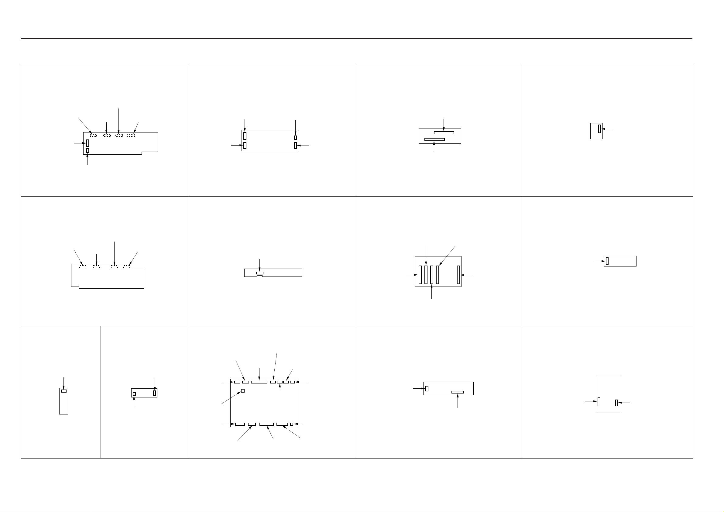
7065 ELECTRICAL PARTS LAYOUT DRAWING
DIAGRAMS
31
37
3
26
17
4
5
30
7
8
6
10
9
11
38
35
36
40
55
43
42
53
45
54
32
60
44
41
39
57
61
12
1
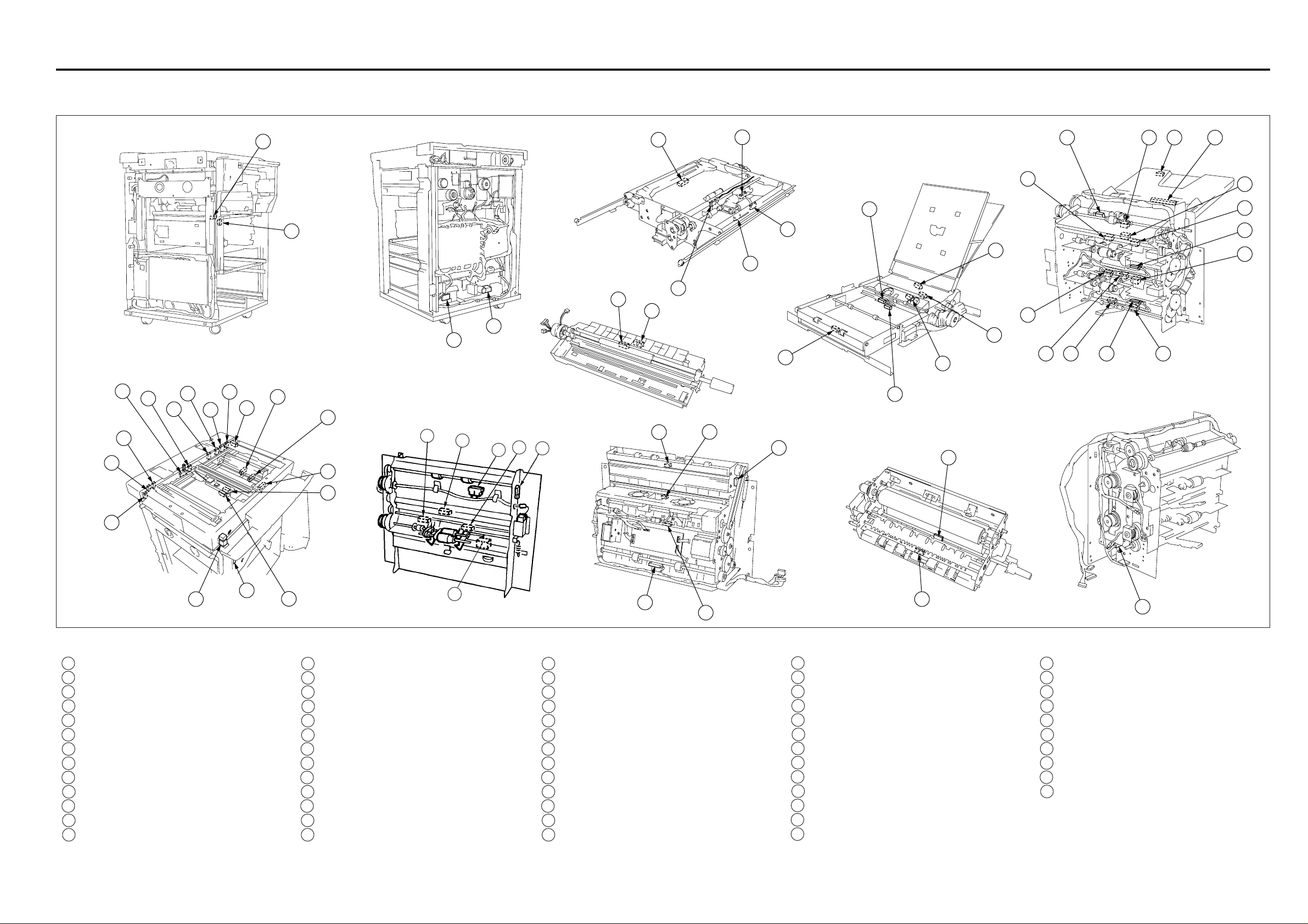
1. Switch Sensor
1 SW1 Main switch
2 MS1 Interlock MS1
3 MS4 Fixing unit set interlock MS4
4 MS141 LCT interlock (1500)
5 MS142 LCT interlock (1000)
6 PS2 Scanner brake PS
7 PS3 Shading position PS
8 PS4 Paper feed restart PS
9 PS5 Optics return PS
10 PS7 Optics timing PS
11 PS8 Glass detection PS
12 PS9 ADF home position PS
13 PS10 Optic syncs PS 2
33
2
34
14 PS11 Paper conveyance door PS
15 PS12 Upper tray no paper PS
16 PS13 Lower tray no paper PS
17 PS14 Registration PS
18 PS15 By-pass no paper PS
19 PS16 Upper limit PS (upper)
20 PS17 Upper limit PS (lower)
21 PS18 No feed PS
22 PS19 Optics sync. PS 1
23 PS20 Pre try PS (upper)
24 PS21 Pre try PS (lower)
25 PS22 By-pass paper size PS
26 PS24 Fixing set PS
46
58
59
27 PS25 Prefeed PS (upper)
28 PS26 Prefeed PS (lower)
29 PS27 Fixing unit paper exit PS
30 PS28 Scan EE PS
31 PS29 ADF brake PS
32 PS30 By-pass PS
33 PS40 APS sensor 1
34 PS41 APS sensor 2
35 PS42 APS sensor 3
36 PS43 APS sensor 4
37 PS45 APS timing PS
38 PS48 APS sensor 7
39 PS140 LCT no paper PS (1500)
40 PS141 LCT no paper PS (1000)
41 PS142 LCT upper limit PS (1500)
42 PS143 LCT upper limit PS (1000)
43 PS144 LCT conveyance PS (1000)
44 PS145 LCT prefeed PS (1500)
45 PS146 LCT conveyance PS (1500)
46 PS147 LCT prefeed PS (1000)
47 PS151 ADU no paper PS
48 PS152 ADU paper feed PS
49 PS153 ADU reversal detection PS
50 PS154 ADU paper exit PS 1
51 PS155 ADU paper exit PS 2
52 PS156 ADU paper exit PS 3
53 PS160 LCT interlock PS
54 PS200 LCT pre try PS (1500)
55 PS210 LCT pre try PS (1000)
56 PS301 Reversal point PS
57 PS302 Reversal paper feed point PS
58 PS303 ADU gate PS
59 PS304 ADU paper feed PS
60 PS305 Reversal paper exit PS
61 PS306 Reversal paper exit interlock PS
62 VR1 By-pass tray paper size VR
3 - 1
Page 3
DIAGRAMS
55
50
32
33
51
56
6
17
16
39
5
4
42
62
45
43
44
46
47
52
18
19
60
40
41
28
61
53
14
10
12
9
8
11
26
31
57
24
34
25
15
13
48
59
54
49
2
35
36
3738
27
30
20
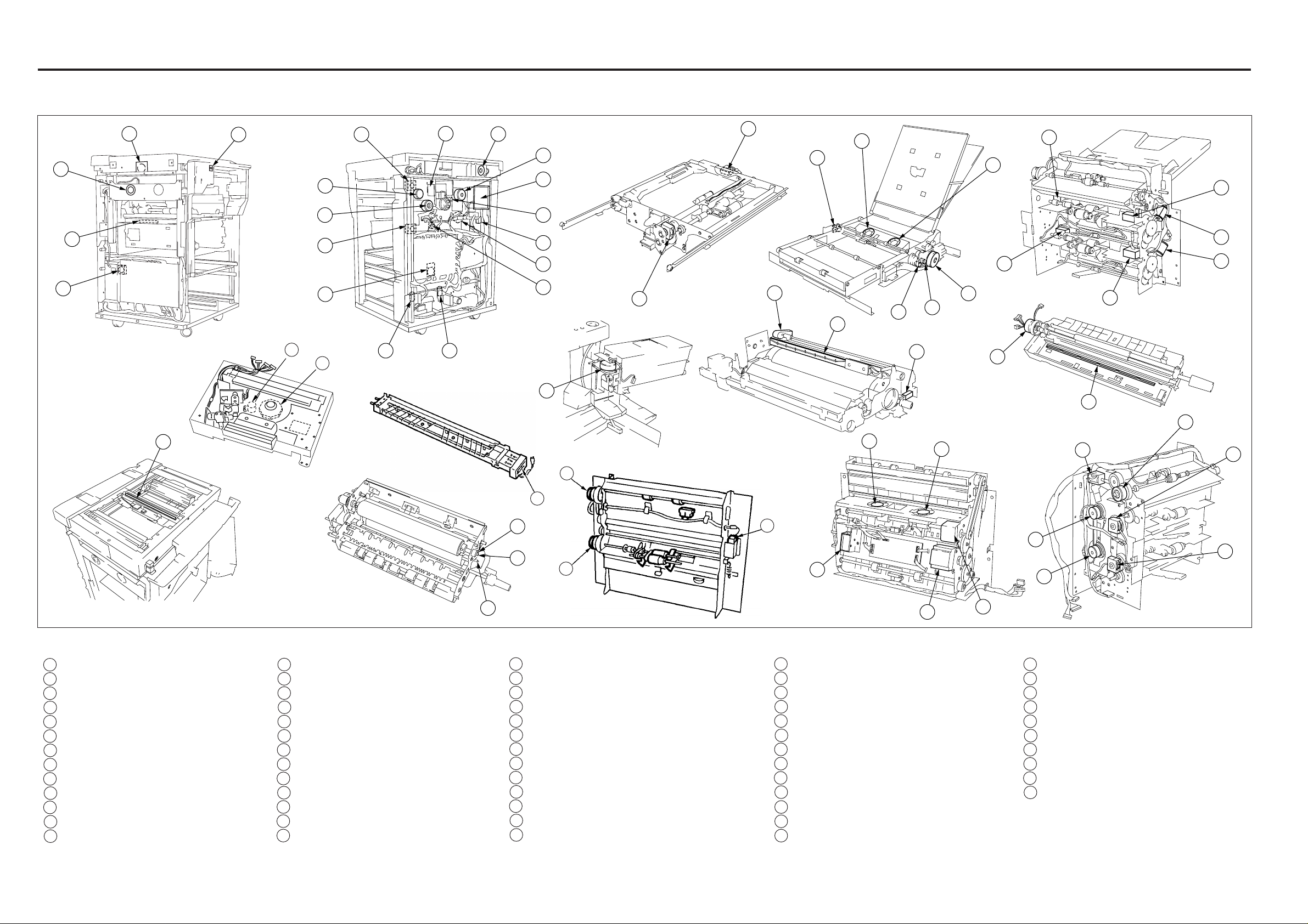
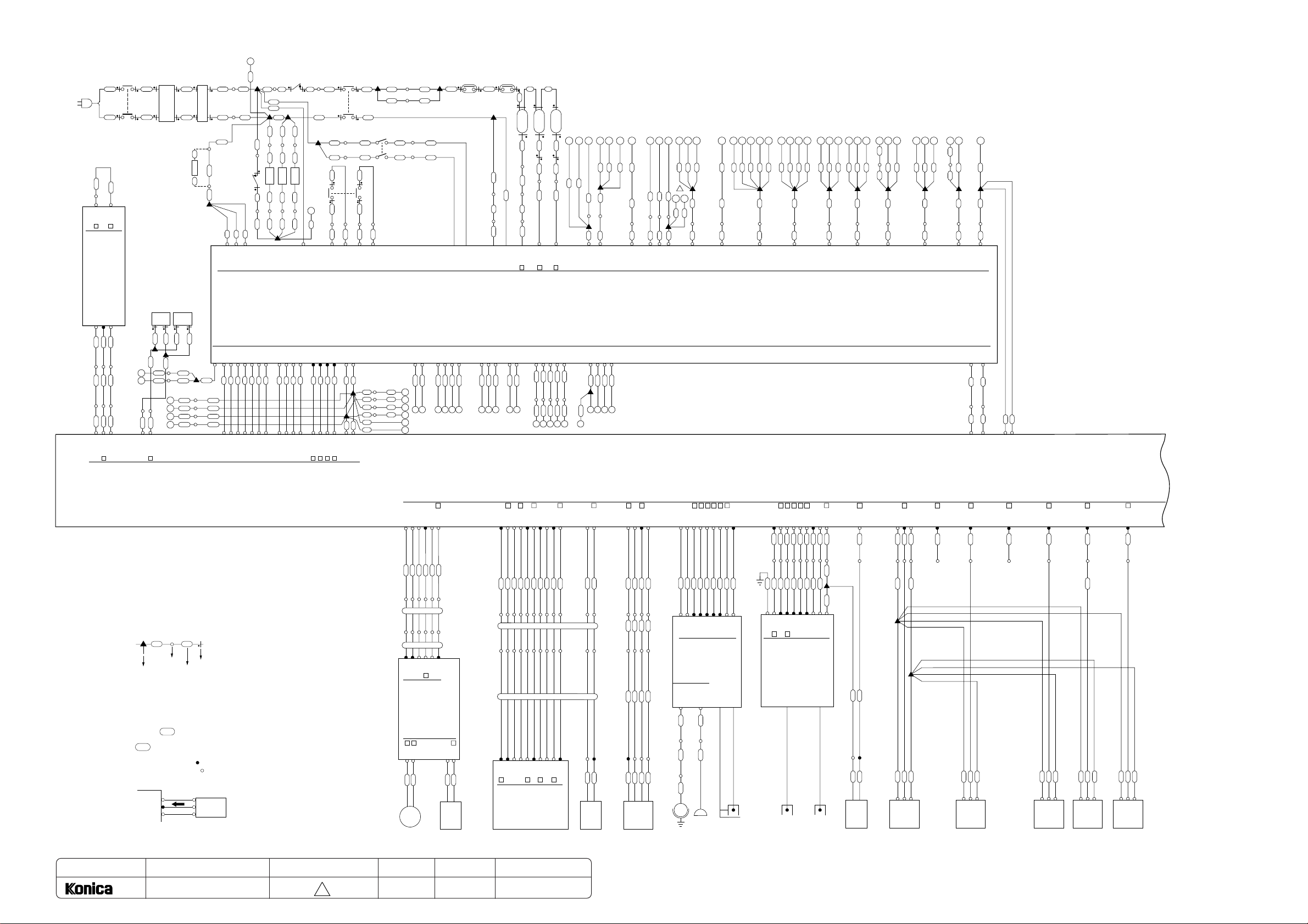
2. Load
1 CL1 LCT 1st paper feed CL (1000)
2 CL2 LCT 1st paper feed CL (1500)
3 CL3 LCT conveyance CL
4 CL151 ADU paper feed CL
5 CL152 ADU reversal CL
6 CL153 ADU timing CL
7 C(K) Key counter
8 C(T) Total counter
9 FM2 Optics cooling fan
10 FM3 DCPS cooling fan
11 FM11 Polygon cooling fan
12 FM14 Conveyance suction fan
13 FM16 Main body cooling fan
14 FM22 E-RDH cooling fan
15 FM30 Developing suction fan
16 FM153 ADU cooling fan 1
17 FM154 ADU cooling fan 2
18 FM203 Paper exit fan 1
19 FM204 Paper exit fan 2
20 L1 Exposure lamp
21 L2 Fixing heater lamp 1
22 L3 Fixing heater lamp 2
23 L4 Fixing heater lamp 3
24 M1 Main motor
25 M3 Developing drive motor
26 M4 Drum motor
3
29
22
21
1
23
27 M5 Polygon motor
28 M7 Charger cleaning motor
29 M8 Transfer/separation cleaning motor
30 M10 Toner supply motor
31 M12 Optics drive motor
32 M17 Upper tray motor
33 M18 Lower tray motor
34 M35 Agitator screw motor
35 M40 Laser correction motor
36 M140 LCT paper feed motor
37 M141 LCT tray motor (1500)
38 M142 LCT tray motor (1000)
39 M151 ADU paper feed motor
58
40 M201 Reversal paper exit motor
41 M202 Paper exit motor
42 MC3 2nd paper feed MC
43 MC5 Paper feed MC (upper)
44 MC6 Paper feed MC (lower)
45 MC7 Paper feed MC (by-pass)
46 MC8 Middle conveyance MC1
47 MC9 Middle conveyance MC2
48 MC10 Cleaner MC
49 MC11 Assist drive MC
50 SD1 1st paper feed SD (upper)
51 SD2 1st paper feed SD (lower)
52 SD3 1st paper feed SD (by-pass)
53 SD4 Separation claw SD
54 SD5 Conveyance SD
55 SD6 Upper tray SD
56 SD7 Lower tray SD
57 SD140 LCT paper feed SD (1500)
58 SD141 LCT paper feed SD (1000)
59 SD153 Paper exit gate SD
60 SD160 Reversal gate SD
61 PCL Pre-charging lamp
62 TSL Transfer Synchronization lamp
3 - 2
Page 4
8
14
32
6
26
DIAGRAMS
13
10
2
27
5
11
33
12
7
19
29
18
16
15
4
22
30
24
17
20
3
37
35 34 38
9
1
23
25
21
28
36 39
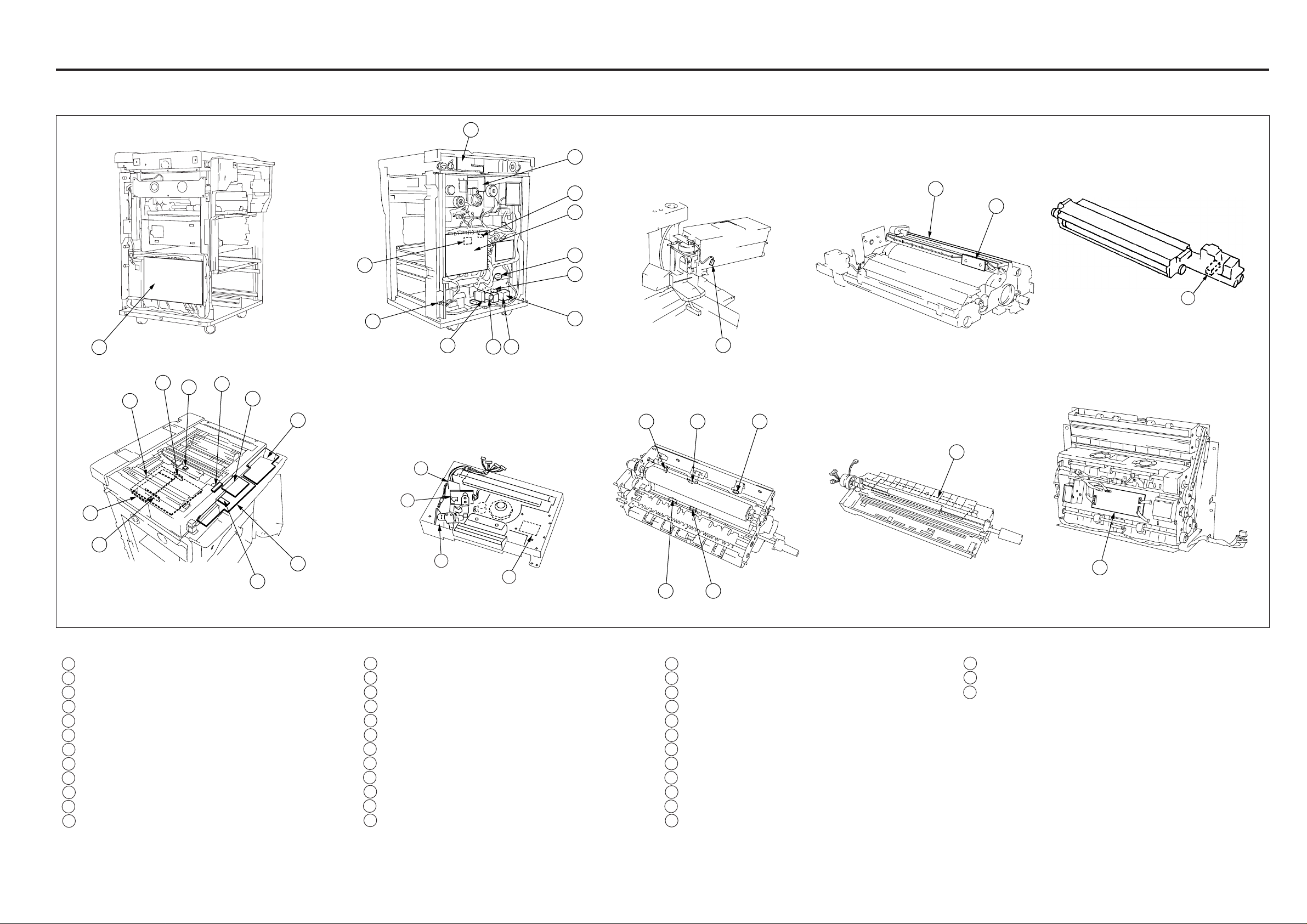
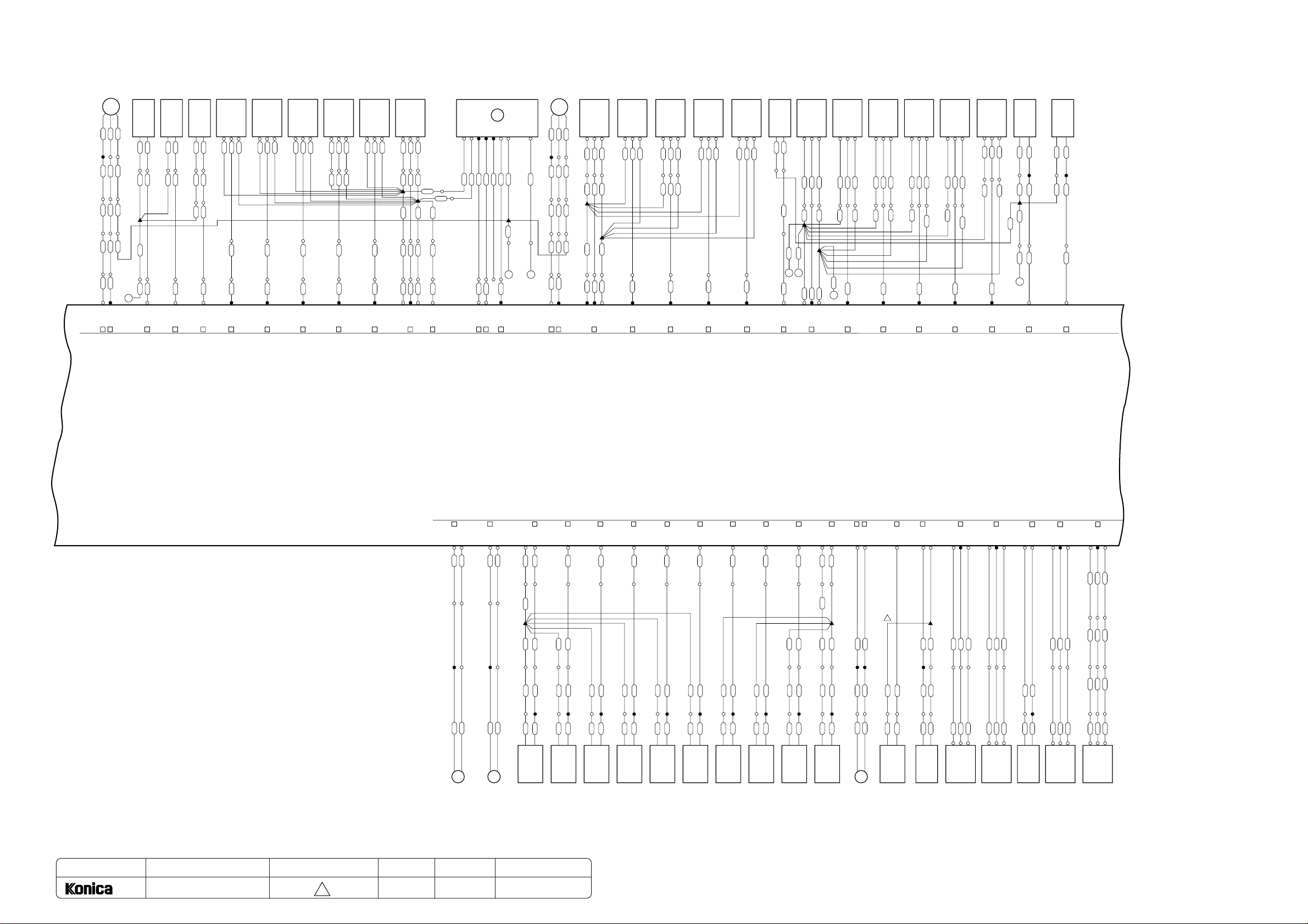
3. Others
1 ADB AD conversion board
2 CB Control board
3 CBR Circuit breaker
4 COIL1 Coil 1
5 COIL2 Coil 2
6 DB Drum board
7 DCPS DC power supply unit
8 EPFDB Paper exit drive board
9 E-RDH Electronic RDH processing board
10 HTR1 Internal heater 1
11 HTR2 Internal heater 2
12 HTR3 Internal heater 3
3 - 3
13 HV1 High voltage unit 1
14 HV2 High voltage unit 2
15 INDICATING BOARD
16 INDICATING STARTER
17 INDEXSB Index sensor board
18 INVB Inverter board
19 IPB Image processing board
20 LDB1 Laser driver board 1
21 LDB2 Laser driver board 2
22 NF Noise filter
23 OB1 Operation board 1
24 OB2 Operation board 2
25 OB3 Operation board 3
26 OPMDB Optics motor drive board
27
–
Paper size detection board
28 PMDB Polygon drive board
29 RDH IFB E-RDH I/F board
30 RL1 Main relay
31
––
32 TCSB Toner control sensor board
33 TDS Toner density sensor
34 TH1 Fixing temperature sensor 1
35 TH2 Fixing temperature sensor 2
36 TH3 Fixing temperature sensor 3
37 TLD Toner level detection sensor
38 TS1 Thermostat 1 (upper)
39 TS2 Thermostat 2 (lower)
Page 5
DIAGRAMS
383
(W:4PIN)
41
(BK:2PIN)
134
(W:3PIN)
133
(W:3PIN)
232(BK:3PIN)
138(W:3PIN)
219(W:10PIN)
222(BK:7PIN)
137(BK:3PIN)
110(BK:3PIN)
72(BK:3PIN)
111(BK:3PIN)
75(BK:3PIN)
113(BK:4PIN)
236(W:3PIN)
130(W:3PIN)
235(W:3PIN)
239
(W:3PIN)
74
(W:3PIN)
67
(W:3PIN)
73
(W:3PIN)
66
(W:3PIN)
76
(W:3PIN)
)
)
)
)
)
392(B:19PIN)
40(W:3PIN)
90(W:3PIN) 610(W:3PIN)
7065 CONNECTOR LAYOUT DRAWING
49(BK:4PIN)
37(W:3PIN)
125(BK:8PIN)
101(W:6PIN)
119(W:12PIN)
237(BK:4PIN)
399(W:2PIN)
53(W:2PIN)
233(W:2PIN)
463(W:4PIN)
48(BK:4PIN)
326(BK:4PIN)
11(BK:4PIN)
169(W:2PIN)
56(W:6PIN)
44(R:8PIN)
44(W:3PIN)
92(W:8PIN) 142(W:7PIN)
163(W:9PIN) 92(W:8PIN) 102(BK:7PIN)
731
(W:2PIN)
734
(W:2PIN)
462
(W:3PIN)
735
(BK:2PIN)
753
(W:2PIN)
327
(W:3PIN)
47
(W:3PIN)
13
(W:3PIN)
732
(W:2PIN)
465
(W:3PIN)
122
(BK:2PIN)
58
(W:3PIN)
152(W:3PIN)
752(W:4PIN)
750
(BK:2PIN)
97(BK:4PIN)
167(BK:2PIN
16(BK:4PIN)
98(BK:4PIN)
91(W:2PIN)
121(BK:8PIN
3(R:8PIN)
123(BK:5PIN
1(R:8PIN)
128(BK:4PIN
387(W:2PIN)
96(BK:4PIN)
475(W:3PIN)
733(BK:4PIN
753(BK:2PIN)
727
(W: 12 PIN)
730 (W: 2 PIN)
723
(W: 3 PIN)
726
(W: 3 PIN)
727 (W: 3 PIN)
724 (W: 3 PIN)
725 (W: 3 PIN)
721 (BK: 3 PIN)
111(BK:12PIN)
234(W:2PIN)
464(W:2PIN)
231(R:2PIN)
110(W:9PIN)
68(BK:8PIN)112(W:13PIN)
230(W:2PIN)
209(BK:5PIN)
52(W:3PIN)
206(W:2PIN)
38(BK:8PIN)
728 (BK: 10 PIN)
23(W:2PIN)
202(W:3PIN)
79(BK:7PIN)
720 (W: 2 PIN)
24(W:2PIN)
207(W:2PIN)
729 (W: 3 PIN)
203(W:3PIN)
123(BK:2PIN)
45(W:3PIN)
328
(W:3PIN)
147
(W:3PIN)
69
(W:3PIN)
141
(W:3PIN)
59
(W:3PIN)
25(BK:7PIN)
54
(W:3PIN)
[How to read connector numbers]
1. Inscribed contents
Connector No.
100
(W: 3 PIN)
Number of pins
Connector color
2. Color code
BN: Brown
R: Red
O: Orange
Y: Yellow
GN: Green
LB: Light blue
S: Silver
B: Blue
V: Violet
GY: Gray
W: White
BK: Black
P: Pink
As an example, (B/W) indicates that the male side of the
connector is blue and the female side white.
3 - 4
Page 6

DIAGRAMS
3
(W: 20 pin)
6
(W: 24 pin)
223
(B: 11 pin)
62
(W: 22 pin)
5
(W: 24 pin)
489
(W: 16 pin)
402
(W: 18 pin)
481
(BK: 24 pin)
61
(W: 9 pin)
30
(W: 24 pin)
65
(W: 22 pin)
83
(W: 24 pin)
200
(W: 20 pin)
120
(BK: 24 pin)
1
(W: 5 pin)
106
(W: 8 pin)
114
(W: 7 pin)
60
(W: 20 pin)
800
(W: 24 pin)
801
(W: 16 pin)
36
(W: 10 pin)
135
(W: 11 pin)
57
(B: 16 pin)
322
(W: 8 pin)
144
(W: 16 pin)
7
(W: 24 pin)
140
(BK: 20 pin)
208
(NC)
4
(W: 8 pin)
9
(W: 18 pin)
22
(W: 16 pin)
35
(W: 5 pin)
78
(W: 7 pin)
88(W: 5 pin)
99
(W: 5 pin)
28
(W: 5 pin)
2
(W: 10 pin)
401
(W: 4 pin)
400
(W: 9 pin)
382
(W: 5 pin)
398
(W: 4 pin)
397
(W: 6 pin)
395
(W: 4 pin)
396
(W: 5 pin)
8
(W: 10 pin)
709(BK:18PIN) 716(BK:2PIN)
532(W:3PIN)
553(W:2PIN)
534(W:3PIN)
712(W:3PIN)715(W:3PIN) 714(BK:2PIN) 713(W:3PIN)
711(W:3PIN)
710(W:3PIN)
523(W:3PIN) 526(W:4PIN) 557(W:3PIN) 556(W:3PIN)
550(W:3PIN)
Control Board
51(BK:5PIN) 34(BK:2PIN)
50
(W: 4 PIN)
17(W:3PIN)
12(W:5PIN)
559(R:3PIN)
524
(R:RPIN)
616(BK:4PIN)
619(W:6PIN)
600(W:6PIN)
618(W:2PIN)
601
(W:12PIN)
617(BK:4PIN)
558
(R:3PIN)
(W:8PIN)
555
(W:3PIN)
614(W:3PIN)
522
(W:8PIN)
505
(BK:24PIN)
611(W:3PIN)
622(W:7PIN)612(W:3PIN)602
525(BK:4PIN)
551(R:2PIN)
552(W:2PIN)
531
(W:13PIN)
613(W:3PIN)
615(W:3PIN)
604(W:6PIN)
603(W:7PIN)
620(BK:6PIN)
621(W:12PIN)
85
(W:11PIN)
42
(R:10PIN)
DCPS
86
(W:2PIN)89(BK:2PIN)46(W:3PIN)32(W:3PIN)
168
(BK: 2 PIN)
3 - 5
Page 7
DIAGRAMS
Operation Board/1
210
(BK: 24 pin)
212
(W: 8 pin)
Operation Board/2
221
(W: 5 pin)
(W: 10 pin)
213
(W: 14 pin)
215
(W: 4 pin)
225
(NC)
10
214
(BK: 24 pin)
217
(W: 10 pin)
216
(W: 3 pin)
Optics Drive Board E-RDH I/F Board
226
(W: 5 pin)
224
(W: 11 pin)
Toner Control Board
19
(W: 10 pin)
225
(W: 3 pin)
228
(W: 10 pin)
RDH Processing Board
454
(W: 144 pin)
(W: 100 pin)
450
(W: 100 pin)
453
(W: 144 pin)
Index Detection Board
428
442
(W: 11 pin)
LD Drive Board
451
(W: 144 pin)
440
(W: 12 pin)
450
(W: 100 pin)
Operation Board/3 Image Processing Board
220 (W: 10 pin)
INDICATING STARTER
77 (W: 4 pin)
71 (W: 3 pin)
430
(W: 4 pin)
431
(N.C.)
427
(N.C.)
425
(W: 24 pin)
426
(N.C.)
428
(W: 100 pin)
422
(W: 12 pin)
421
(W: 12 pin)
420
(W: 34 pin)
423
(W: 12 pin)
465
(W: 50 pin)
424
(W: 8 pin)
467
(W: 16 pin)
452
(W: 144 pin)
AD Converter Board Polygon Driver Board
410
(W: 5 pin)
432
411
(W: 40 pin)
(W: 12 pin)
320
(W: 8 pin)
3 - 6
Page 8
7065 OVERALL WIRING DIAGRAM (1/5)
1
MAIN RELAY
AC POWER
CBR
BK BK
WW
L1
∗
385-4
385-1
∗
LV
HV
INVB
752-1 752-3 752-4
COIL2
BK BK
752-2
W
W W W W
∗
NF
∗
∗
∗
∗
COIL1
COIL1
(KBE ONLY)
∗
390-2 390-1
∗
∗
398-3
AC(C)
RL2
(KBJ ONLY)
SUB RELAY
753-2 753-1
∗
∗
397-5
397-6
AC(H)
AC(C)
BK
∗
BK
BK
W
∗
387-2
750-2
WWW
HTR3
∗
BK
387-1
750-1
BKBKBK
W
W
HTR2
BK
RL1
∗
W
751-2
HTR1
BK
2
751-1
BK
398-1
AC(H)
MS4
BK BK BK BK
BK BK
MAIN SWITCH
BK
395-1
AC(H)
381-3
BK
BK
W W
W
396-3
AC(C)
381-4
SW1
W
395-2
AC(C)
383-1
BK
383-2
BK
MS1
BK BK
∗
381-1
381-2
BK
396-1
AC(H)
BK
BK
392-9
392-10
383-3
383-4
∗∗∗
BK
BK
397-1
AC(H)
TS-2 TS-1
BK
W
394-2
∗
399-2
W
397-2
AC(H)
AC(H)
W
382-1
AC(C)
∗
L2
W
392-18
GY
394-1
∗
399-1
V
∗
L2 DRIVE
L3
W
392-19
BN BNBNBN
382-2
∗
L3 DRIVE
L4
W
392-20
382-4
∗
L4 DRIVE
4036 37 41 42 43 44 45 46 47 48 49 50 52 53 54
∗∗∗
∗∗
∗
∗
∗
∗
122-1
122-2
122-3
∗
∗
∗
78-1
78-2
78-3
24V DC
24V DC
24V DC
∗
122-4
122-5
∗∗∗
78-4
24V DC
∗
78-5
24V DC
122-6
∗
38 39
78-6
PGND
∗∗∗
2
∗
∗
∗
121-1
∗
78-7
PGND
51
∗∗∗∗∗
∗
121-3
∗
99-2
24V DC
57 58 59 60
55 64 66
∗∗∗
∗
∗
121-4
∗
99-3
24V DC
121-5
∗
∗
99-4
PGND
61 63
6256
∗
∗∗∗∗∗
121-6
65 67 69
∗
123-2
∗
99-5
PGND
∗
∗
∗
88-2
PGND
68 70 72
∗
∗
128-2
∗∗
∗
123-3
∗
88-3
PGND
71 73
∗∗∗
∗
123-4
∗
88-4
40V DC (1)
∗∗
∗
128-1
∗
123-574121-2
∗
88-5
40V DC (1)
75
∗
∗
∗
99-1
24V DC
29-3
29-2
29-1
∗∗∗∗
232-2
232-1
∗∗∗
470-1 232-3
470-2
470-3
∗∗∗
60-B8
60-A9
60-A10
H
PGND
24V DC
L1 CONT
[How to see the diagram]
1. The signals shown reflect levels present
under normal idleing conditions with
the main switch turned ON.
2. Wiring symbols in the figure are
as follows.
(1) [Symbol]
(2) [Color code]
Example: represents
green yellow striped pattern.
(3) is ribbon cable.
(4) Signal flow
The solid black circle ( ) among
the connector symbols ( )
indicates the direction of signal flow.
Example)
RL1 RL2
BBR
∗∗
3
∗∗∗
4
81-1
81-2
∗
60-B9
60-B10
L
24V DC
RL DRIVE
Connector
PGC
BN - Brown
R - Red
O - Orange
Y - Yellow
GN - Green
LB - Light blue
Y/GN
RC
CB
5VDC
PS1
SGND
∗
96-1
96-3
∗∗
5
∗
6
∗
7
∗
8
∗
50-1
VV
Wire (Violet)
B - Blue
V - Violet
GY- Gray
W - White
BK- Black
P - Pink
Direction of
signal flow
R
24V DC (2)
24V DC (2)
PGND
12V DC
SGND
SGND
5V DC
8V DC
5V DC (For control board)
2-2
2-1
2-3
2-4
2-5
2-6
2-8
2-10
8-10
∗∗∗∗∗∗∗∗∗∗∗∗∗∗∗∗∗
96-4
∗
96-5
∗
96-6
∗
96-7
∗
4-1
61-5
61-7
61-9
Faston
61-1
61-2
61-3
61-4
PS1
5V DC (For control board)
SGND
SGND
8-9
8-7
8-6
8-4
8-3
4-2
4-4
4-5
60-B7
60-A6
L
L
L2 CONT
RL1 CONT
8-2
8-1
60-A7
60-A8
H
H
L3 CONT
L4 CONT
SGND
2-7
∗
61-6
5V DC
2-9
∗
61-8
DCPS
5V DC
5V DC
11V DC (For KRDS)
SGND
SGND
SGND
PGND
PGND
PGND
24V DC
24V DC
5V DC
-5V DC
SGND
SGND
12V DC
40V DC
PGND
12V DC
SGND
401-1
401-2
8-8
8-5
401-3
401-4
28-1
28-2
28-3
28-5
28-6
400-6
400-8
400-7
400-9
400-5
400-1
400-2
400-3
400-4
412-3
412-5
26
27 28 29 30
412-2
412-4
412-1
∗∗∗∗∗
∗∗∗∗∗
35
∗
31 32 33 34
∗
∗∗∗
∗
100-1
∗
100-2
∗
101-2
∗
101-3
∗
∗
∗
∗
9
∗
10
∗
11
∗
12
∗
13
14
∗∗∗
∗
∗
∗
∗∗∗
2524232221201918171615
121-7
99-6 PGND
∗
∗
1-4
123-1
88-1 PGND
∗
∗
1-3
∗
∗
1-2
1-1
CB (1/5)
TDS CONT
12VDC
TDS ANG
SGND
24VDC
PGND
B CONT
C CONT
C SHIFT
B SHIFT
G SHIFT
M7 DRIVE 1
30-B7
∗∗∗∗∗
63—3
63—4
50—3
50—4
21—1
21—2
M7 DRIVE 1
∗
39—1
R
M7
CHARGER
CLEANING
MOTOR
5VDC
M7 DRIVE 2
5-A1
5-A2
30-B8
63—5
63—6
RC
50—5
50—6
RC
21—3
21—4
∗
TH2 ANG
M7 DRIVE 2
∗
39—2
BK
24VDC
PCL CONT
L
5-A3
5-A4
∗
63—7
63—8
50—7
50—8
21—5
21—6
CHARGING
DB
PRE-
LAMP
24VDC
PCL CONT
L
20—1
20—2
R
W
γ / Dmax LED V ref
12VDC
∗
5-A12
5-A11
5-B1
Y
∗
∗
324—1
324—2
324—3
325—1
325—2
325—3
19—1
19—2
19—10
∗
γ sig / MONI
Dmax LED CONT
DRUM JAM CONT
L
L
5-B2
5-B3
5-B4
∗
324—4
324—5
324—6
325—4
325—5
325—6
19—3
19—4
19—5
∗
Dmax MONI
TCBS
TONER
CONTROL
SENSOR
5-B5
∗∗∗
324—7
324—8
RC
325—7
325—8
RC
19—6
∗
Dmax sig
SGND
5-B6
5-B7
B
324—9
325—9
19—7
19—8
DRUM JAM
LED CONT
L
5-B8
∗
∗
324—10
325—10
19—9
∗
24VDC
SD 4 DRIVE
L
5-B9
5-B10
O
∗
324—11
324—12
325—11
325—12
34—1
34—2
B
R
SD4PCL
SEPARATION
CLAW
SOLENOID
∗
5-A5
5-A6
Y
∗
63—9
63—10
∗∗∗
50—12
50—13
∗∗∗
51—1
51—2
R
BN
DENSITY
SENSOR
∗
5-A7
∗
63—11
50—14
51—3
O
5-A8
B
63—12
∗
50—15
∗
51—4
Y
GP CONT
L
L
L
∗∗∗
62-A11
62-A2
62-A3
62-A4
62-A5
62-A6
62-A7
62-A8
62-A9
B
O
∗∗∗
∗
∗∗∗
84—1
84—2
84—3
84—4
84—5
84—6
84—7
84—8
84—9
L
F SIG
GP
71—1
GUIDE
PLATE
HV1
31—2
BN
∗
CHARGING
31—1 BIAS
GY
GY
50—20 70—1
GY
BIASTONER
S SHIFT (DC)
S SHIFT (AC)
S CONT
T SHIFT
T CONT
PGND
62-B5
85—5
24VDC
L
L
∗
62-B4
62-B3
62-B2
62-B1
O
B
85—4
85—3
85—2
85—1
L
∗
∗
62-B10
62-B8
62-B7
62-B6
∗∗∗∗∗∗∗
85—10
85—8
85—7
85—6
∗
∗∗∗
∗
∗∗∗
∗
∗
∗
87—1
87—3
87—5
87—6
87—7
87—8
87—9
87—10
87—11
T SIG
HV2
HV2
87—12
SYNCHRONIZATION
∗
∗
F.G
S SIG
SEPARATE TRANSFER TRANSFER
89—1
LAMP
85—9
∗
89—2
R
PSL CONT
∗
62-B11
∗
∗
W
5VDC
PS40
L
22-A5
22-A6
R
∗
163-1
163-2
∗
133-3
133-2
PS40TSLTDS
APS
SENSOR 1
163-3
SGND
22-A7
B
∗
∗∗∗
133-1
∗∗∗
134-1
PS47
L
22-A2
∗
163—8
NC
PS42
L
22-B1
∗
163—5
130-3
130-2
APS
SENSOR 3
∗∗∗
130-1
PS46
H
22-A1
163—7
NC
PS41
L
22-AB
∗
∗
163—4
134-3
134-2
PS41 PS42 PS43
APS
SENSOR 2
PS48
L
22-A3
∗∗
163—9
239-3
239-2
PS48
APS
SENSOR 7
∗∗∗
239-1
PS43
L
22-B2
∗
163—6
138-3
138-2
APS
SENSOR 4
∗∗∗
138-1
MODEL
7065
MANUAL
SERVICE HANDBOOK
REVISED EDITION
3 - 7
2
DATE
Jan.2000
PAGE
3-7
METHOD
REPLACEMENT
Page 9

7065 OVERALL WIRING DIAGRAM (2/5)
DEVELOPING
CLEANER
CLUTCH
MC10
∗
167-1
∗
30-B1 30-B2
24VDC
DEVELOPING
SCREW
MOTOR
161-1
∗
167-2
∗
54
H
MC 10 DRIVE
161-5
161-3
∗
∗
O
30-A6
30-A7
∗∗
P
M35 PLL
M35 DRIVE
161-2
61
SUCTION
FAN
Y
R
11-1
11-2
∗
∗
B
65-A1
65-A2
H
H
FM30 LD
FM30 DRIVE
CONVEYANCE
SUCTION
FAN
Y
R
BK
BN
15-1
15-2
11-3
11-4
∗
∗
∗
B
49
59
65-A3
65-A10
65-A11
H
H
FM14 LD
FM30 H/L
FM14 DRIVE
BK
15-3
B
POLYGON
COOLING
FAN
Y
R
BN
48-1
48-2
48-3
∗
∗
O
53
65-A4
65-A5
∗
H
FM11 LD
FM11 H/L
48-4
58
BK
B
DCPS
COOLING
FAN
FM3
Y
R
237-1
237-2
237-3
∗
55
30-B5
H
FM3 LD
BK
BN
2
237-4
∗
∗∗
∗
48
56 63
30-B4
∗
FM3 H/L
TONER
SUPPLY
MOTOR
14-1
14-5
14-3
∗ ∗
12-4
12-5
12-6
∗
O
30-B11
30-B12
P
L
M10 PLL
M10 DRIVE
14-2
∗∗
12-7
∗
B
E-RDH
COOLING
FAN 2
Y
R
BN
49-1
49-2
49-3
∗
∗
O
3
65-A6
65-A7
∗
H
FM22 LD
FM22 H/L
FAN
OPTICS
COOLING
FAN
MAIN BODY
COOLING
FM2M10 FM16FM11FM14FM30 FM22M35
R
Y
R
BK
49-4
B
57 52 50 60
16-1
2
16-2
O
65-B9
FM16 LD
BN
16-3
∗
∗
65-B10
∗
H
FM16 H/L
BK
16-4
B
113-1
113-2
97-1
97-2
∗
128-3
128-4
∗∗
83-A1
H
FM2 DRIVE
Y
BK
113-4
∗∗ ∗
97-4
∗
B
83-B1
H
FM2 LD
2
204-1
∗∗∗∗∗∗∗
74
69
MAIN
MOTOR
DRUM
MOTOR
M1 M4 M3
2
204-2
205-1
30-A1
5VDC
205-3
205-4
30-A3
30-A4
H
H
M1PLL
M1 CONT
205-5
30-A5
SGND
205-2
30-A2
P
M1 CLK
62
51
201-8
201-10
201-1
201-2
201-3
∗∗∗∗∗∗∗
125-8
125-7
125-1
125-2
125-3
∗∗∗∗∗∗∗
124-8
124-7
124-1
124-2
124-3
∗∗∗∗∗∗∗
30-A8
30-A9
30-A10
H
5VDC
SGND
M4 CONT
201-5
125-5
124-5
30-B6
∗
M4 H/L
201-4
125-4
124-4
30-A11
P
M4 CLK
201-6
217-1
217-2
∗
∗∗∗∗∗∗∗∗∗∗∗
125-6
∗
124-6
∗
65-B3
65-B4
30-A12
H
5VDC
SGND
M4 PLL
DEVELOPING
DRIVE
MOTOR
217-3
217-4
217-5
217-6
65-B5
65-B6
65-B7
P
H
∗
M3 H/L
M3 CLK
M3 CONT
217-7
65-B8M3 LD
H
NC
217-8
65
217-9
66
217-10
70
217-11
71
321-1
321-2
321-3
PPPPP
M5 DRIVE A
M5 DRIVE B
M5 DRIVE C
320-1
320-2
320-3
∗
∗
95-1
95-2
95-3
322-1
322-2
322-3
P
H
SGND
M5 CLK
M5 CONT
POLYGON
MOTOR
M5
321-5
321-6
321-7
PPP
M5 MAG A
M5 MAG A’
M5 MAG B’
PMDB
M5 RDY
∗
320-4
320-5
320-6
∗∗∗
95-4
95-5
95-6
∗∗∗∗∗
322-4
322-6
∗
M5 RDY
M5 BREAK
321-8
321-9
M5 MAG B
M5 MAG C’
320-8
320-7
∗∗∗
95-7
95-8
321-10
321-11
P
P
V MAG-
M5 MAG C
4 35 68
326-3
326-2
∗∗∗
326-1
∗∗∗
12VDC
22-B3
Y
12-1
∗∗∗
TLD
∗
22-B4
∗
12-2
SGND
22-B5
B
12-3
22-B7
∗
L
22-B8
∗
SGND
9-A1
B
92-1
∗
92-2
PS2
L
9-A2
∗
5VDC
9-A3
R
92-3
CB(2/5)
L
9-A9 PS8
∗
92-4
∗
92-5
9-A5 PS4
L
∗
92-6
L
9-A6 PS5
∗
92-7
L
9-A7 PS7
∗
9-B3 PS28L65-B1 24V DC
∗
∗
92-8
H
65-B2 MC11 DRIVE
∗
142-3
∗
L
9-B9 PS29
∗
∗
L
9-B2 PS9
∗
142-1
∗
∗∗∗
L
2
9-A4 PS3
∗
142-2
2
∗
∗
9-B6 SGND
142-4
∗
L
9-B7 PS45
∗∗∗
142-5
142-6
9-B8 5VDC
∗
∗
144-A1 PS22
∗
110-1
∗
∗∗∗
152-2
152-1
152-3
463-3
∗
∗
∗∗∗
∗
∗∗∗
∗
463-2
∗∗∗
∗
144-A3 VR1
∗
110-2
∗
463-1
∗
463-4
111-1
79-1
L
7-B1 PS12
7-B11 SGND
∗
∗
111-1
∗
∗
∗∗∗
79-2
∗
∗∗∗
79-3
7-A11 5VDC
∗
111-12
∗
∗
∗
L
7-B3 PS16
∗
111-3
∗
79-4
∗∗∗
L
7-B9 PS20
∗
111-9
∗
79-5
∗∗∗
L
7-B6 PS19
∗
111-6
∗∗∗
2
68-2
68-1
∗∗∗
68-3
209-3202-1
144-A7 PS25
∗
110-4
∗∗∗
209-4
∗
∗
202-2
∗∗∗
209-5
∗
202-3
203-1
144-B7 PS26
∗
110-5
∗
68-5
∗∗∗
203-2
∗∗∗
144-A5 PS10
∗
110-3
∗
68-4
203-3
∗∗∗
111-2
∗
25-1
∗
∗∗∗
25-2
L
7-B2 PS13
∗
∗
25-3
L
7-B4 PS17
∗
111-4
∗
∗
25-4
L
7-B10 PS21
∗
111-10
∗
25-5
38-6
∗
L
7-B5 PS18
111-5
38-7
L
7-B7 PS15
∗
∗
∗
111-7
∗
38-8
L
7-B8 PS11
∗
111-8
∗
∗∗∗
∗∗∗
∗∗∗
∗∗∗
∗∗∗
17-1
17-2
17-3
∗∗∗
TONER
LEVEL
DETECTION
41-1
41-2
R
BK
TOTAL
COUNTER
∗∗∗
76-1
76-2
PS2 PS8 PS4 PS7PS5C (T)TLD
SCANNER
BRAKE
SENSOR
76-3
∗∗∗
67-1
67-2
GLASS
SENSOR
67-3
PAPER FEED
∗∗∗
73-1
73-2
RESTART
SENSOR
73-3
∗∗∗
66-1
66-2
OPTICS
RETURN
SENSOR
66-3
∗∗∗
74-1
74-2
OPTICS
TIMING
SENSOR
74-3
∗∗∗
110-1
110-2
PS28
SCAN
EE
SENSOR
110-3
169-1
169-2
∗
MC11
ASSIST
DRIVE
CLUTCH
∗
111-1
111-2
111-3
PS29
ADF-BRK
SENSOR
75-1
75-2
PS9
OPTICS
ADF-HP
SENSOR
75-3
72-1
72-2
72-3
PS3
OPTICS
SHADING
DETECTOR
137-1
137-2
PS45
APS
TIMING
SENSOR
137-3
462-1
462-2
PS22
BY-PUS
PAPER
SIZE
SENSOR
462-3
465-3
VR1
BY-PUS
PAPER
SIZE
DETECTING
VR
MODEL
465-2
465-1
NO PAPER
7065
58-1
58-2
44-1
44-2
44-3
PS12
UPPER
TRAY
SENSOR
58-3
PS16
UPPER
LIMIT
SENSOR
(UPPER)
327-1
327-2
PS20
PRE W
TRY
SENSOR
(UPPER)
MANUAL
SERVICE HANDBOOK
327-3
141-1
141-2
141-3
PS19
OPTICS
SYNC
SENSOR 1
54-1
54-2
54-3
69-1
69-2
69-3
147-1
PS25
PRE-FEED
SENSOR
(UPPER)
PS26
PRE-FEED
SENSOR
(UPPER)
PS10
OPTICS
SYNC
SENSOR 2
REVISED EDITION
3 - 8
2
147-2
147-3
45-1
45-2
45-3
PS13
LOWER
TRAY
NO PAPER
SENSOR
DATE
Jan.2000
59-1
59-2
59-3
PS17
UPPER
LIMIT
SENSOR
(LOWER)
328-1
328-2
PS21
PRE W
TRY
SENSOR
(LOWER)
PAGE
3-8
13-1
13-2
328-3
13-3
PS18
NO FEED
SENSOR
REPLACEMENT
47-1
47-2
47-3
PS15
BY-PASS
NO PAPER
SENSOR
METHOD
52-1
52-2
52-3
PS11
PAPER
CONVEYANCE
DOOR
SENSOR
Page 10
7065 OVERALL WIRING DIAGRAM (3/5)
ADU
COOLING
FAN 1
FM153
∗
∗
∗
525-4
525-2
∗∗∗
523-1
523-2
523-4
∗∗∗
522-2
522-4
522-1
∗
∗
∗
505-11
505-9 525-1
∗
∗
83-B10
83-B11
∗
H
FM153 LD
FM153 DRIVE
ADU
PAPER
FEED
CLUTCH
CL151
∗
∗
551-1
551-2
∗
∗
∗
505-1
505-2
∗
∗
44
83-A4CL151 DRIVEH83-A5CL152 DRIVE
H
ADU
REVERSAL
CLUTCH
CL152
∗
∗
552-1
552-2
∗
∗
505-3
∗
ADU
TIMING
CLUTCH
CL153
∗
553-1
553-2
∗
531-1
531-2
∗
505-4
83-A6CL153 DRIVE
H
∗
∗
∗
∗
ADU
NO PAPER
SENSOR
PS151
550-3
550-2
550-1
∗∗∗
531-4
∗
505-18
∗
57-B3PS151
H
ADU
PAPER
FEED
SENSOR
PS152
555-3
555-2
∗∗∗
531-5
∗
505-5
∗
57-A1PS152
H
REVERSAL
DETECTION
555-1
ADU
SENSOR
PS153
556-3
556-2
556-1
∗∗∗
531-6
∗
505-6
∗
57-A2PS153H57-A3PS154
H
ADU
PAPER
EXIT
SENSOR 1
PS154
557-3
557-2
557-1
∗∗∗
532-3
532-1
532-2
∗∗∗
531-7
∗
505-7
∗
ADU
PAPER
EXIT
SENSOR 2
PS155
558-3
558-2
558-1
∗∗∗
531-8
∗
505-8
∗
57-A4PS155
H
ADU
PAPER
EXIT
SENSOR 3
PS156
559-3
559-2
559-1
∗∗∗
534-1
534-2
∗∗∗
∗
∗
531-11
531-9
531-10
∗∗∗
505-13 534-3
505-12
505-10
∗∗∗
57-B45VDC
57-A5PS156
57-B6SGND
H
554-1
554-2
554-3
∗∗∗∗∗
∗
531-13
∗
531-12
∗
531-3
∗∗
505-23
505-14
∗
57-A8ADU SW
L
ADU
PAPER
FEED
MOTOR
M151
554-4
554-5
554-6
505-15
505-16
505-17
∗∗∗
83-A8M151 DRIVE
83-A9M151 CLOCK
83-A11M151 LD
P
H
H
554-8
∗
∗
505-20
47 40
554-11
∗
505-22
ADU
COOLING
FAN 2
FM154
∗∗∗
526-4
526-2
∗∗∗
524-2
524-4
524-1
∗∗∗
522-6
522-8
522-5
∗
∗
∗
505-21
505-19 526-1
∗∗
∗
83-B12
83-A12
H
FM154 LD
FM154 DRIVE
REV-FEED
POINT
SENSOR
PS302
611-1
611-3
611-2
∗∗∗
619-1
619-2
619-3
∗∗∗
∗
∗
622-1
622-2
622-7
∗∗∗
200-A4
200-A1
200-A10
H
5V DC
PS302
S GND
ADU
GETE
SENSOR
PS303
612-3
612-2
∗∗∗
622-3
∗
200-A5
H
PS303
612-1
AUD
PAPER
FEED
SENSOR
PS304
613-3
613-2
∗∗∗
619-4
619-5
619-6
∗∗∗
622-4
∗
200-A6
H
PS304
613-1
REV-PAPER
EXIT
SENSOR
PS305
614-3
614-2
614-1
∗∗∗
622-5
∗
200-A7
H
PS305
INTER
LOCK
SENSOR
PS306
615-3
615-2
615-1
∗∗∗
622-6
∗
200-A8
H
PS306
LCT 1ST
NO PAPER
PAPER FEED
SOLENID
(10)
SD141
∗
∗∗
721-1
721-2
728-4
∗
777876
∗
120-B11SD141 DRIVE
H
LCT PAPER
LCT
UPPER LIMIT
(10)
723-1
723-2
∗∗∗
728-6
∗
723-3
728-7
∗
SENSOR
(10)
PS143
724-1
724-2
∗∗∗
728-8
728-9
728-10
∗
SENSOR
PS141
728-5
∗
∗
∗
∗∗∗
83-B3SGNDH83-B4PS141
83-B55VDCL83-B6PS143L83-B7PS160
INTERLOCK
SENSOR
PS160
724-3
∗
LCT
725-1
∗∗∗
722-1
∗
722-2
CONVEYANCE
725-3
725-2
722-3
∗
∗
LCT
SENSOR
(10)
PS144
727-1
727-2
∗
∗
722-6
722-4
722-5
∗
∗
83-B8PS144
H
727-3
∗∗
LCT
PRE W
SENSOR
(10)
PS210
726-1
726-2
726-3
∗∗∗∗
722-7
722-8
722-9
∗
83-B9PS210
∗
∗
LCT
PRE-FEED
SENSOR
(10)
PS147
729-1
729-2
729-3
∗∗∗
722-10
722-11
722-12
∗
∗
∗
83-A10PS147
H
LCT
CNVEYANCE
CLUTCH
CL3
∗
∗
730-1728-1
730-2
∗∗∗∗
728-3
∗
∗
41
120-B9CL3 DRIVE
H
LCT 1ST
PAPER FEED
CLUTCH
(10)
CL1
∗
∗
720-1
720-2
∗
∗
728-2
∗
120-B10CL1 DRIVE
H
CB(3/5)
H
7-A1 M17 DRIVE
7-A2 24VDCH7-A3 M18 DRIVE
∗
∗
110-6
110-7
110-8
23-1
24-1
23-2
∗
∗
∗
24-2
∗
7-A4 24VDC
∗
110-9
∗
24V DC
7-A5
∗∗
112-1
∗
79-6
∗
122-1
∗
SD1 DRIVE
H
7-A6
∗
112-2
∗∗∗
79-7
∗
122-2
∗
24V DC
∗
∗
∗
∗
112-10
∗
38-5
∗
206-2
∗
114-B3
∗∗
112-11
∗
209-1
∗
207-1
∗
7-A7 SD2 DRIVEH7-A8 SD3 DRIVEH7-A12 MC7 DRIVEH7-A9 MC5 DRIVEH7-A10 MC6 DRIVEH7-B12 MC8 DRIVEH114-A4 MC9 DRIVEH114-B2 SD6 DRIVEH114-B4 SD7 DRIVE
∗
25-6
∗
123-1
∗
112-3
25-7
∗
123-2
∗
53-1
∗
112-4
∗
∗
53-2
∗
∗
∗
233-1
∗
∗
112-7
∗
233-2
∗
∗
230-1
∗
∗
112-5
∗
230-2
∗
∗
231-1
∗
∗
112-6
∗
231-2
∗
234-1
∗
112-8
∗
∗
234-2
∗
∗
∗
464-1
∗
∗
112-9
∗
464-2
∗
38-4
206-1
H
∗
112-12
∗
209-2
∗
207-2
∗
∗
∗
30-B9 M8 DRIVE 1
30-B10 M8 DRIVE 2
∗
∗
42-4
42-5
∗
∗
168-1
168-2
∗
∗
2
91-1
∗
91-2
∗
H
6-A10 SD153 DRIVE
40-3
∗
64-2
∗
H
6-B11 SD5 DRIVE
6-B10 24V DC
∗
∗
40-1
∗
∗
64-1
∗
∗
6-A1 SGND
∗∗∗
42-1
42-2
∗∗∗
H
6-A2 PS14
43-3
6-A3 5VDC
6-A4 SGND
42-8
H
6-A5 PS30
∗∗∗
42-9
∗∗∗
5V DC
6-A6
42-10
H
6-A7 24VDC
6-A8 MC3 DRIVEL6-B8 PS24
∗
∗
86-1
86-2
∗
∗
6-A9 SGND
∗∗∗
82-1
∗∗∗
82-2
82-3
6-B9 5VDC
3-B1 5V DC
∗∗∗
98-11
98-10
∗∗∗
392-7
392-15
∗∗∗
90-2
90-1
∗∗∗
H
6-A11 PS301
98-12
392-16
90-3
3-B3 SGND
MODEL
7065
MANUAL
SERVICE HANDBOOK
REVISED EDITION
3 - 9
2
DATE
Jan.2000
M17
UPPER
TRAY
MOTOR
PAGE
3-9
SD1
M18
LOWER
TRAY
MOTOR
1ST
PAPER
FEED
SOLENOID
(UPPER)
METHOD
REPLACEMENT
SD2
1ST
PAPER
FEED
SOLENOID
(LOWER)
SD3
1ST
PAPER
FEED
SOLENOID
(BY-PASS)
MC7
PAPER
FEED
CLUTCH
(BY-PASS)
MC5
PAPER
FEED
CLUTCH
(UPPER)
MC6
PAPER
FEED
CLUTCH
(LOWER)
MC8
MIDDLE
CNVEYANCE
CLUTCH
1
MC9
MIDDLE
CNVEYANCE
CLUTCH
2
SD6
UP
TRAY
SOLENOID
SD7
LOU
TRAY
SOLENOID
M8
TRANSFER
/SEPARATE
CLEANING
MOTOR
SD153
EXIT GATE
SOLENOID
SD5
CNVEYANCE
SOLENOID
46-1
46-2
46-3
PS14
REGIST.
SENSOR
32-1
32-2
32-3
PS30
BY-PASS
SENSOR
MC3
2ND
PAPER
FEED
CLUTCH
37-1
37-2
PS24
FUSER
DETECT
SENSOR
37-3
610-1
610-2
610-3
PS301
REV
POINT
SENSOR
Page 11

7065 OVERALL WIRING DIAGRAM (4/5)
LCT 1ST
PAPER FEED
CLUTCH (15)
CL2
∗
∗
716-1
716-2
∗
∗
709-1
709-2
43
∗
120-B1
H
CL2 DRIVE
LCT 1ST
PAPER FEED
SOLENID (15)
SD140
∗
714-1
714-2
∗
∗
709-9
709-4
42
∗
120-B2
H
SD140 DRIVE
LCT
710-1
∗
710-2
710-3
∗
LCT PAPER
UPPER LIMIT
SENSOR (15)
711-1
∗
NO PAPER
SENSOR (15)
PS140 PS142 PS146 PS200
∗
∗∗∗
709-5
709-6
709-7
711-2
∗∗
709-8
SENSOR (15)
711-3
∗
LCT
PRE-FEED
PS145
715-1
715-2
∗∗∗
∗∗
709-16
CONVEYANCE
SENSOR (15)
715-3
2
∗∗∗
120-B3
SGND
120-B4
H
PS140
120-B5
5VDC
120-B6
L
PS142
120-B12
H
PS145
LCT
713-1
∗
709-3
713-2
∗
∗
120-B7
H
PS146
713-3
∗
LCT
PRE W
SENSOR (15)
712-1
712-2
∗
∗
∗
709-10
709-12
709-11
77 78
∗
120-B8
∗
PS200
712-3
∗
∗
LCT PAPER
FEED MOTOR
703-3
703-1
∗
709-15
73 76
40VDC
703-2
67
204-1
PGND
M140
2
204-2
204-3
∗∗∗∗∗∗∗∗∗
120-A1
5VDC
204-4
204-5
204-6
120-A2
120-A3
120-A4
P
∗
SGND
M140 PLL
M140 CONT
CB (4/5)
LCT
TRAY
MOTOR (15)
M141 M142
∗
∗
731-1
731-2
∗
∗
46
120-A5
120-A6
L
P
M140 CLOK
M141 DRIVE
LCT
TRAY
MOTOR (10)
∗
∗
732-1
732-2
∗
∗
45
120-A7
L
M142 DRIVE
LCT TRAY
DETECTOR (15)
MS141 MS142
∗∗
735-2
709-14
709-13
∗
733-2
∗
∗
2
735-1
∗
∗
733-1
∗
120-A9
120-A8
P
P
TMP4
TRAY (15) ADD
LCT TRAY
DETECTOR (10)
∗
∗
734-1
734-2
∗
∗
120-A10
120-A11
P
P
TMP4
TRAY (10) ADD
DCPS
30
29 26 28 27
∗∗∗∗∗
410-1
410-2
410-3
410-4
410-5
5VDC
SGND
TCK2
ACKTGCLAMP
411-2
411-3
420-33
420-32
411-4
420-31
411-5
420-30
GND
411-6
420-29
SGND
S CK
411-7
420-28
S IN
411-8
420-27
—5VDC
S LD
MD 0
411-9
411-10
420-26
420-25
MD 1
411-11
420-24
MD 2
411-12
420-23
GND
411-13
420-22
OD 0
411-14
420-21
OD 1
411-15
420-20
OD 2
411-16
420-19
OD 3
411-17
420-18
12VDC
TCK1
PPPPPPPPPPPPPPPPPPPPPPPPPPPPP
411-1
420-34
OD 4
411-18
420-17
OD 5
411-19
RC
420-16
OD 6
411-20
420-15
OD 7
411-21
420-14
ADB
OD 8
411-22
420-13
GND
411-23
420-12
ED 0
411-24
420-11
ED 1
411-25
420-10
ED 2
411-26
420-9
ED 3
411-27
420-8
ED 4
411-28
420-7
ED 5
411-29
420-6
ED 6
411-30
420-5
IPB (1/2)
ED 7
411-31
420-4
ED 8
411-32
420-3
APR
P
411-33
420-2
GND
411-34
420-1
LASER
REVISE MOTOR
M40
Y
O
W
BK
GY
443-1
443-2
443-3
443-4
443-6
∗∗∗∗∗∗∗
424-1
424-2
424-3
424-4
424-5
PPPPP
M40 PWR A
M40 PWR B
M40 DRIVE A
M40 DRIVE B
M40 DRIVE A’
IP REQ
INDEX
TXA 1
∗
425-A1
425-A2
425-A3
425-A4
425-A5
∗∗∗∗∗∗∗
442-1
442-2
442-3
BN
443-5
424-6
424-7
424-8
423-1
423-2
∗
SMPR
425-A9
425-A10
425-A11
5VDC
425-A12
423-3
PPP
SGND
M INDEX 1
MPR
425-B1
P
∗
HLVL
M40 DRIVE B’
425-A6
425-A7
∗∗∗∗∗∗∗∗∗∗∗∗∗
INDXSB LDB1 LDB2
442-4
442-5
442-6
442-7
442-8
423-4
SGND
425-B2
RC
423-5
M INDEX 2
TXA 0
425-B3
425-B4
423-6
SGND
425-B5
442-9
423-7
423-8
423-9
P
SGND
S INDEX 1
S INDEX 2
425-B6
425-B7
442-10
423-10
SGND
425-B8
∗
423-11
∗
HLVL
425-B9
423-12
∗
IPR
O YOBI 1
425-B10
425-B11
∗
∗
∗
425-B12
∗
440-1
421-1
5VDC
440-2
421-2
SGND
440-3
440-4
440-5
440-6
RC
421-3
421-4
421-5
421-6
∗
∗
H
SGND
LD1 VIDEO
LD1 APC CONT 1
LD1 APC CONT 2
440-7
421-7
H
LD1 ALM
440-8
440-9
421-8
421-9
P
∗∗∗
LD1 INC
LD1 IRCLK
440-10
421-10
LD1 U/D
440-11
421-11
LD1 C/S
440-12
421-12
∗
LD1 LPR
441-1
422-1
5VDC
441-2
422-2
SGND
441-3
441-4
441-5
441-6
RC
422-3
422-4
422-5
422-6
∗
∗
H
SGND
LD2 VIDEO
LD2 APC CONT 1
LD2 APC CONT 2
441-7
422-7
H
LD2 ALM
441-8
441-9
422-8
422-9
P
∗∗∗
LD2 INC
LD2 IRCLK
441-10
422-10
LD2 U/D
441-11
441-12
422-11
422-12
∗
LD2 C/S
LD2 LPR
DCPS
17 18 19 20
∗∗∗
430-1
430-2
430-3
5VDC
5VDC
SGND
∗
430-4
SGND
TH1 ANG 1
TH1 ANG 2
∗
∗
6-B1
6-B2
∗
∗
98-1
98-2
98-3
∗
∗
392-1
392-2
392-3
∗∗∗
TH1
FIXING
TEMPERATURE
SENSOR 1, 2
TH2 ANG 1
TH2 ANG 2
TH3 ANG 1
∗
∗∗∗
6-B3
6-B4
6-A12
∗∗∗
98-4
98-5
∗∗∗
392-5
392-4
∗
∗
TH2
TH3 ANG 2
6-B12
∗∗
98-6
392-6
∗
TH3
SENSOR
SGND
6-B5
∗∗∗
98-7
98-8
∗∗∗
392-12
392-13
∗∗∗
40-1
PS27
FIXING
EXIT
PS27
L
6-B6
40-2
5VDC
6-B7
98-9
392-14
40-3
M12 H/L
M12 CLK
M12 STOP
M12 MODE 0
M12 MODE 1
M12 MODE 2
M12 F/R
M12 CONT
∗
223-4
∗
223-5
∗
223-6
HHH
223-7
223-8
M12 BRAKE
223-9
P
223-1
∗
223-2
∗
223-3
∗∗∗∗∗∗∗∗∗∗∗
224-1
224-2
224-3
224-4
224-5
224-6
224-7
224-8
224-9
M12 DRIVE C
M12 DRIVE A
M12 DRIVE B
M12 MAG A’
M12 MAG A
M12 MAG B’
M12 MAG B
M12 MAG C’
PPPPPPPPP
225-1
225-2
225-3
WWW
M12 MAG C
228-1
228-2
228-3
228-4
228-5
228-6
BKBKBKBKBKBKBKBKBK
M12
OPTICS DRIVE MOTOR
M12 NCR
M12 PLLL
∗
223-10
223-11
224-10
224-11M12 PLL
∗
SGND
5VDC
228-7
228-8
M12 FG
∗
228-9
OPMDB
2
40VDC
PGND
12VDC
226-1
226-2
226-3
∗∗∗ ∗
31 32 33
DCPS
481-A1
481-A2
481-A3
481-A4
481-A5
481-A6
481-A7
481-A9
481-B1
481-B2
481-B3
481-B4
481-B5
481-B6
481-B7
481-B8
P
RXA 1
SGND
MTN V/V
MAPC CAL
481-B9
481-B10
∗
∗∗∗
∗
CORR
MIND CHG
481-B11
481-B12
SV
GND
3-A7
∗
SD LE DRIVE
WT LE DRIVE
∗
∗
3-A8
3-A9
∗
∗
SGND
3-A10
∗
SGND
3-B5
∗
8VDC
3-B6
∗
5VDC
3-B7
∗
OB1 TXD
P
3-A1
∗
219-1
∗
10-1
3-A2
∗
219-2
∗
10-2
P
OB1 RXD
OB1 RTS
P
3-A3
∗
219-3
∗
10-3
219-4
3-A4
∗
219-5
∗
10-4
P
OB1 CTS
OB1 DTR
P
3-A5
∗
219-6
∗
10-5
3-A6
5678
∗
∗∗∗
219-7
219-8
∗
10-6
10-7
P
5VDC
OB1 DSR
∗
10-8
5VDC
219-9
∗
∗
10-9
SGND
219-10
∗
∗
10-10
SGND
P
P
∗∗∗∗∗
SGND
RESET
M V/V
MEE V/V
481-A10
DCORR
I YOBI 1
481-A11
481-A12
GND
8VDC
P
P
∗
RXA 0
OB1
5VDC
S LE
G LE
SS LE
EXT LE
JSD 0
JSD 5
JSD 6
JSL 14
217-8
220-8
217-9
220-9
NC
217-10
220-10
Y1 CONT
X1 CONT
Y2 CONT
X2 CONT
FL HOTNCNC
FL GND
LCD Vajd
24VDC
LD3
LD2
LD1
LD0
24VDC
PGND
5VDCCPLP
213-9
82-9
∗
213-10
82-10
∗
213-11
82-11
FLMNCDISP OFF
∗
∗
212-12
213-13
213-14
82-12
82-13
82-14
217-1
220-1
217-2
220-2
217-3
220-3
217-4
220-4
217-5
217-6
217-7
RC
220-5
220-6
220-7
SGND
226-5
222-4
∗
221-1
222-5
221-2
P
P
P
213-3
82-3
213-4
82-4
213-5
82-5
P
213-6
82-6
213-7
82-7
213-8
RC
82-8
222-6
222-7
222-3
222-2
222-1
210-1
210-2
210-3
210-4
210-5
210-6
210-7
210-8
210-9
210-10
210-11
210-12
210-13
210-14
210-15
210-16
210-17
210-18
210-19
210-20
210-21
210-22
210-23
210-24
∗
∗
∗
221-3
221-4
∗
215-1
∗
215-2
∗
215-4
214-1
214-2
214-3
214-4
214-5
214-6
214-7
214-8
RC RC
214-9
214-10
214-11
214-12
214-13
214-14
214-15
214-16
214-17
214-18
214-19
214-20
214-21
214-22
214-23
214-24
∗∗∗∗∗
212-1
212-2
212-3
212-4
83-1
83-2
83-3
83-4
212-5
212-6
-1
-2
∗∗∗∗∗∗
212-7
-3
212-8
-4
∗∗
∗
213-1
82-1
213-2
82-2
∗
34
WT SW
OB2
LMP ADJ
SGND
216-1
216-2
RC
71-1
71-2
5VDC
216-3
71-3
INDICATING BOARD
FL
FL GND
R
BK
77-1
77-4
OB3
INDICATING STARTER
MODEL
7065
MANUAL
SERVICE HANDBOOK
REVISED EDITION
3 - 10
2
DATE
Jan.2000
PAGE
3-10
METHOD
REPLACEMENT
Page 12

7065 OVERALL WIRING DIAGRAM (5/5)
1
MAIN RELAY
AC POWER
CBR
BK BK
WW
L1
∗
385-4
385-1
∗
LV
HV
INVB
752-1 752-3 752-4
COIL2
BK BK
752-2
W
W W W W
∗
NF
∗
∗
∗
∗
COIL1
COIL1
(KBE ONLY)
∗
390-2 390-1
∗
∗
398-3
AC(C)
RL2
(KBJ ONLY)
SUB RELAY
753-2 753-1
∗
∗
397-5
397-6
AC(H)
AC(C)
BK
∗
BK
BK
W
∗
387-2
750-2
WWW
HTR3
∗
BK
387-1
750-1
BKBKBK
W
W
HTR2
BK
RL1
∗
W
751-2
HTR1
BK
2
751-1
BK
398-1
AC(H)
MS4
BK BK BK BK
BK BK
MAIN SWITCH
BK
395-1
AC(H)
381-3
BK
BK
W W
W
396-3
AC(C)
381-4
SW1
W
395-2
AC(C)
383-1
BK
383-2
BK
MS1
BK BK
∗
381-1
381-2
BK
396-1
AC(H)
392-9
392-10
383-3
BK
383-4
BK
TS-2 TS-1
397-1
AC(H)
397-2
AC(H)
BK
394-2
399-2
W
∗
W
AC(H)
W
382-1
AC(C)
∗
L2
W
392-18
GY
394-1
∗
399-1
V
∗
L2 DRIVE
L3
W
392-19
BN BNBNBN
382-2
∗
L3 DRIVE
L4
W
392-20
382-4
∗
L4 DRIVE
∗
∗∗∗
BK
BK
4036 37 41 42 43 44 45 46 47 48 49 50 52 53 54
∗∗∗
∗∗
∗
∗
∗
122-1
122-2
122-3
∗
∗
∗
78-1
78-2
78-3
24V DC
24V DC
24V DC
∗
122-4
122-5
∗∗∗
78-4
24V DC
∗
78-5
24V DC
122-6
∗
78-6
PGND
∗∗∗
2
38 39
∗
51
∗∗∗∗∗
∗
121-1
∗
78-7
PGND
∗
121-3
∗
99-2
24V DC
∗
57 58 59 60
55 64 66
∗∗∗
∗
∗
121-4
∗
99-3
24V DC
121-5
∗
∗
99-4
PGND
61 63
6256
∗
∗∗∗∗∗
121-6
65 67 69
∗
123-2
∗
99-5
PGND
∗
∗
∗
88-2
PGND
68 70 72
∗
∗
128-2
∗∗
∗
123-3
∗
88-3
PGND
71 73
∗∗∗
∗
123-4
∗
88-4
40V DC (1)
∗∗
128-1
123-574121-2
88-5
40V DC (1)
75
∗
∗
∗
∗
∗
∗
99-1
24V DC
3
4
81-1
60-B10
24V DC
∗∗
81-2
∗
60-B9
L
RL DRIVE
RL1 RL2
BBR
∗
96-1
∗∗∗
96-3
5
6
7
8
R
24V DC (2)
2-2
∗∗
96-4
∗
∗
96-5
∗
∗
96-6
∗
∗
96-7
∗
∗
24V DC (2)
PGND
12V DC
SGND
SGND
5V DC
8V DC
5V DC (For control board)
2-1
2-3
2-4
2-5
2-6
2-8
2-10
8-10
∗∗∗∗∗∗∗∗∗∗∗∗∗∗∗∗∗
61-1
61-2
61-3
4-1
61-4
61-5
61-7
61-9
29-3
29-2
29-1
∗∗∗∗
232-2
232-1
∗∗∗
470-1 232-3
470-2
470-3
∗∗∗
60-B8
60-A9
60-A10
H
PGND
24V DC
L1 CONT
5V DC (For control board)
SGND
SGND
8-9
8-7
8-6
8-4
8-3
4-2
4-4
4-5
60-B7
60-A6
L
L
L2 CONT
RL1 CONT
8-2
8-1
60-A7
60-A8
H
H
L3 CONT
L4 CONT
SGND
2-7
∗
61-6
5V DC
2-9
∗
61-8
DCPS
5V DC
5V DC
11V DC (For KRDS)
SGND
SGND
SGND
PGND
PGND
PGND
24V DC
24V DC
5V DC
-5V DC
SGND
SGND
12V DC
40V DC
PGND
12V DC
SGND
401-1
401-2
8-8
8-5
401-3
401-4
28-1
28-2
28-3
28-5
28-6
400-6
400-8
400-7
400-9
400-5
400-1
400-2
400-3
400-4
412-3
412-5
27 28 29 30
26
412-2
412-4
412-1
∗∗∗∗∗
∗∗∗∗∗
35
∗
31 32 33 34
∗
∗∗∗
∗
100-1
∗
100-2
∗
101-2
∗
101-3
∗
∗
∗
∗
9
∗
10
∗
11
∗
12
∗
13
14
∗∗∗
∗
∗
∗
∗∗∗
2524232221201918171615
121-7
99-6 PGND
∗
∗
1-4
123-1
88-1 PGND
∗
∗
1-3
∗
∗
1-2
1-1
CB (1/5)
TDS CONT
12VDC
TDS ANG
SGND
24VDC
PGND
B CONT
C CONT
C SHIFT
B SHIFT
G SHIFT
M7 DRIVE 1
30-B7
∗∗∗∗∗
63—3
63—4
50—3
50—4
21—1
M7 DRIVE 1
∗
39—1
R
M7
CHARGER
CLEANING
MOTOR
5VDC
M7 DRIVE 2
5-A1
5-A2
30-B8
63—5
63—6
RC
50—5
50—6
RC
21—2
21—3
21—4
∗
TH2 ANG
M7 DRIVE 2
∗
39—2
BK
24VDC
PCL CONT
L
5-A3
5-A4
∗
63—7
63—8
50—7
50—8
21—5
21—6
CHARGING
DB
PRE-
LAMP
24VDC
20—1
R
PCL CONT
L
20—2
W
γ / Dmax LED V ref
∗
5-A12
5-A11
∗
324—1
324—2
324—3
325—1
325—2
325—3
19—1
19—10
∗
γ sig / MONI
12VDC
Dmax LED CONT
L
5-B1
5-B2
5-B3
Y
324—4
324—5
324—6
325—4
325—5
325—6
19—2
19—3
19—4
∗
Dmax MONI
TCBS
TONER
CONTROL
SENSOR
DRUM JAM CONT
SGND
L
5-B4
5-B5
5-B6
5-B7
B
∗
∗∗∗∗∗
324—7
324—8
324—9
324—10
RC
325—7
325—8
325—9
325—10
RC
19—5
19—6
19—7
19—8
∗
∗
Dmax sig
DRUM JAM
LED CONT
L
5-B8
∗
19—9
SEPARATION
24VDC
5-B9
O
324—11
324—12
325—11
325—12
34—1
34—2
R
SD4PCL
CLAW
SOLENOID
SD 4 DRIVE
L
5-B10
∗
B
∗
5-A5
5-A6
Y
∗
63—9
63—10
∗∗∗
50—12
50—13
∗∗∗
51—1
51—2
R
BN
DENSITY
SENSOR
∗
5-A7
∗
63—11
50—14
51—3
O
5-A8
B
63—12
∗
50—15
∗
51—4
Y
GP CONT
L
L
L
∗∗∗
62-A11
62-A2
62-A3
62-A4
62-A5
62-A6
62-A7
62-A8
62-A9
B
O
∗∗∗
∗
∗∗∗
84—1
84—2
84—3
84—4
84—5
84—6
84—7
84—8
84—9
L
F SIG
GP
GUIDE
PLATE
HV1
31—2
BN
71—1
∗
CHARGING
31—1 BIAS
GY
GY
50—20 70—1
GY
BIASTONER
S SHIFT (DC)
S SHIFT (AC)
S CONT
T SHIFT
T CONT
PGND
24VDC
L
L
62-B5
85—5
L
∗
62-B4
62-B3
62-B2
62-B1
O
B
85—4
85—3
85—2
85—1
∗
∗
62-B10
62-B8
62-B7
62-B6
∗∗∗∗∗∗∗
85—10
85—8
85—7
85—6
∗
∗∗∗
∗
∗∗∗
∗
∗
∗
87—1
87—3
87—5
87—6
87—7
87—8
87—9
87—10
87—11
T SIG
HV2
HV2
87—12
SYNCHRONIZATION
∗
∗
F.G
S SIG
SEPARATE TRANSFER TRANSFER
89—1
LAMP
85—9
∗
89—2
R
PSL CONT
∗
62-B11
∗
∗
W
5VDC
PS40
L
22-A5
22-A6
R
163-1
163-2
∗
133-3
133-2
PS40TSLTDS
APS
SENSOR 1
PS46
H
22-A1
∗
NC
PS41
L
22-AB
∗
163—4
PS47
L
22-A2
∗
163—8
NC
SGND
22-A7
B
∗
163—7
163-3
PS42
L
22-B1
∗
163—5
PS48
L
22-A3
∗∗
163—9
PS43
L
22-B2
∗
163—6
∗
138-3
138-2
APS
SENSOR 4
∗∗∗
138-1
∗∗∗
133-1
130-3
130-2
APS
SENSOR 3
∗∗∗
130-1
∗∗∗
134-3
134-2
134-1
PS41 PS42 PS43
APS
SENSOR 2
239-3
239-2
PS48
APS
SENSOR 7
∗∗∗
239-1
MODEL
7065
MANUAL
SERVICE HANDBOOK
REVISED EDITION
3 - 11
2
DATE
Jan.2000
PAGE
3-11
METHOD
REPLACEMENT
Page 13
JAM LIST
Following jam detection is carried out in this machine.
[1] Paper Jam
Classifica-
tion
By-pass
feed tray
Tray 1
Tray 2
Tray 3
Main body and LCT
Tray 4
Jam
code
J10-1
J10-2
J10-4
J11-1
J11-2
J11-3
J11-4
J12-1
J12-2
J12-3
J12-4
J13-1
J13-2
J13-3
J13-4
J14-1
J14-2
J14-3
J14-4
When
stationary
When
operating
When
stationary
When
operating
When
stationary
When
operating
When
stationary
When
operating
When
stationary
When
operating
Causes
PS18 (no feed) and PS14 (registration) are OFF during idling but PS30
(by-pass feed) is ON.
PS14 (registration) or PS30 (by-pass
feed) is not turned ON within 4 seconds from ON of SD3 (by-pass feed).
PS30 (by-pass) is ON at the time of
ON of SD3 (by-pass feed).
PS20 (pre try (upper)) is ON during
idling.
PS20 (pre try (upper)) is not turned
ON within 400 msec from ON of SD1
(1st paper feed (upper)).
PS18 (no feed) is not turned ON
within 650 msec from ON of SD1
(1st paper feed (upper)).
PS20 (pre try (upper)) is ON when SD1
(1st paper feed (upper)) goes ON.
PS21 (pre try (lower)) is ON during
idling.
PS21 (pre try (lower)) is not turned
ON within 400 msec from ON of SD2
(1st paper feed (lower)).
PS18 (no feed) is not turned ON
within 820 msec from ON of SD2
(1st paper feed (lower)).
PS21 (pre try (lower)) is ON when SD2
(1st paper feed (lower)) goes ON.
PS210 (LCT pre try (1000)) is ON
during idling.
PS210 (LCT pre try (1000)) is not
turned ON within 420 msec from ON
of SD141 (LCT paper feed (1000)).
PS144 (LCT conveyance (1000)) is
not turned ON within 2 seconds from
ON of SD141 (LCT paper feed (1000)).
PS210 (LCT pre try (1000)) is ON
when SD141 (LCT paper feed
(1000)) is ON.
PS200 (LCT pre try (1500)) is ON
during idling.
PS200 (LCT pre try (1500)) is not
turned ON within 370 msec from ON
of SD140 (LCT paper feed (1500)).
PS146 (LCT conveyance (1500)) is
not turned ON within 2.4 seconds
from ON of SD140 (LCT paper feed
(1500)).
PS200 (LCT pre try (1500)) is ON
when SD140 (LCT paper feed
(1500)) is ON.
Operation when jam
occurs
If a copy is being
made when a jam
occurs, copy operation
is stopped after
completion of exit of
the copy.
DIAGRAMS
Method of clearing jam
Remove the original
paper from by-pass tray
then remove the jammed
paper.
Open the main body
conveyance door and
remove the jammed
paper and close it.
Open the tray and
remove the jammed
paper and close it.
Open the LCT conveyance door and remove
the jammed paper and
close it.
Open the tray and
remove the jammed
paper and close it.
Open the LCT upper
cover and remove the
jammed paper and close
it.
Open the tray and
remove the jammed
paper and close it.
3 - 13
Page 14

DIAGRAMS
Classifica-
tion
LTC-352
paper feed
jam
LT-352
Conveyance
jam
Main body and LCT
Jam
code
J15-1
J15-2
J15-3
J15-4
J16-0
J17-1
J17-3
J17-4
J17-5
J17-6
J19-0
J19-1
J19-2
When
stationary
When
operating
When
stationary
When
stationary
When
operating
When
operating
When
stationary
Causes
PS802 (LT pre try) is ON during idling.
PS802 (LT pre try) is not turned ON
within 400 msec from ON of MC800
(LT 1st paper feed).
PS18 (no feed) is not turned ON
within 800 msec from ON of PS802
(LT pre tray).
PS802 (LT pre try) is ON when
MC800 (LT 1st paper feed) is ON.
PS14 (register) is ON during idling.
PS18 (no feed) or PS19 (optics sync
1) is ON during idling.
PS19 (optics sync 1) is not turned
ON within 560 msec from ON of
PS156 (ADU paper exit 3).
PS19 (optics sync 1) is not turned
ON within 430 msec from the start of
reconveyance in right lengthwise
conveyance in LCT paper feed.
PS18 (no feed) is not turned ON
within 560 msec from the start of
reconveyance in right lengthwise
conveyance in LCT/ADU reverse
side.
A loop is not completed within 400
msec from ON of PS18 (no feed).
PS144 (LCT conveyance (1000)) is
not turned ON within 2 sec. from ON
of PS147 (LCT prefeed (1000)).
PS146 (LCT conveyance (1500)) is
not turned ON within 2 sec. from ON
of PS145 (LCT prefeed (1500)).
PS144 (LCT conveyance (1000)) or
PS146 (LCT conveyance (1500)) is
ON during idling.
PS147 (LCT prefeed (1000)) or
PS145 (LCT prefeed (1500)) is ON
during idling.
Operation when jam
occurs
If a copy is being made
when a jam occurs,
copy operation is
stopped after completion of exit of the copy.
If a copy is being made
when a jam occurs,
copy operation is
stopped after completion of exit of the copy.
If a copy is being made
when a jam occurs,
copy operation is
stopped after completion of exit of the copy.
Method of clearing jam
Open the LCT conveyance door and remove
the jammed paper and
close it.
Pull the LCT out and
remove the jammed
paper.
Open the front door and
remove the jammed
paper and close it.
Open the conveyance
door and remove the
jammed paper and close
it.
3 - 14
Page 15

DIAGRAMS
Classifica-
tion
Conveyance
jam
Main body and LCT
Jam
code
J21
J30
J31
J32
J33-1
J33-2
J33-3
J33-4
When
stationary
When
operating
When
stationary
When
operating
Causes
TCSB (drum wrapping sensor) is ON.
PS14 (registration) is not turned OFF
within paper size length + 40 mm
from ON of MC3 (2nd paper feed).
PS27 (fixing paper exit) is not turned
ON within 2000 msec from ON of
MC3 (2nd paper feed).
PS27 (fixing paper exit) was turned
ON within 280 msec from copy start.
PS27 (fixing paper exit) is ON during idling.
PS27 (fixing paper exit) does not go
OFF within 2000 msec after PS27
(fixing paper exit) goes ON.
PS301 (reversal point), PS302 (reversal paper feed point), PS303
(ADU gate), PS304 (ADU paper feed)
or PS305 (reversal paper exit) is ON
during idling.
PS301 (reversal point) is not turned
ON within 800 msec from ON of
PS27 (fixing paper exit).
PS301 (reversal point) is not turned
OFF within 2.4 sec. from ON of
PS301 (reversal point).
PS305 (reversal paper exit) is not
turned OFF within 1 sec. from ON of
PS27 (fixing paper exit) at the
straight paper exit.
PS305 (reversal paper exit) is not
turned OFF within 1 sec. from start
of M201’s (reversal paper exit) reversing operation at the reversal
paper exit.
Operation when jam
occurs
The main body is
stopped immediately.
Method of clearing jam
Open the front door and
remove the jammed
paper and close it.
Open the paper exit and
the front door and
remove the jammed
paper and close them.
Open the main body left
plate, remove the jammed
paper, then close it.
3 - 15
Page 16

DIAGRAMS
Classification
DF-312
RADF
Jam
code
J61-0
J61-1
J62-1
J62-2
J62-3
J62-4
J62-5
J63-0
J63-1
J63-2
J63-3
When
stationary
When
operating
When
stationary
When
operating
Causes
MS301 (cover open/close detect) is
ON during idling.
MS301 (cover open and close detect)
was turned ON during RADF operating.
PS301 (DF open and close detect) is
OFF during idling.
PS301 (DF open/close detect) was
turned OFF during RADF operation.
PS306 (original registration) is not
turned OFF within a certain period
after it has been turned ON.
PS308 (original conveyance) is not
turned ON within a certain period
after the pre-feed of the duplex
original front side (include the
simplex original) has been started.
PS308 (original conveyance) is not
turned ON within a certain period
after the pre-feed of the duplex
original back side has been started.
PS308 (original conveyance) is not
turned OFF within a certain period
after the scanning of the duplex
original front side (include the
simplex original) has been started.
PS308 (original conveyance) is not
turned OFF within a certain period
after the scanning of the duplex
original back side has been started.
PS307 (original paper exit) is not
turned ON within a certain period
after the scanning of the simplex
original has been started.
PS307 (original paper exit) is not
turned ON within a certain period
after the scanning of the duplex
original back side has been started.
At the simplex original exiting,
PS307 (original paper exit) is not
turned OFF within a certain period
after it has been turned ON.
At the duplex original exiting,
PS307 (original paper exit) is not
turned OFF within a certain period
after it has been turned ON.
Operation when jam
occurs
RADF is stopped
immediately.
If there is paper during
or after transfer, the
main body is stopped
after exit of the paper.
Jam clearing method
Open the RADF and
remove the jammed
paper and close it.
If there is a jammed
paper on a vertical
conveyance unit in the
main body, remove it.
3 - 16
Page 17

DIAGRAMS
Classification
DF-312
RADF
Jam
code
J63-4
J63-5
J63-6
J63-7
J65-0
J65-1
J65-2
J65-3
When
operating
When
stationary
Causes
PS309 (original reversal detect) is
not turned ON within a certain
period after the scanning of the
duplex original front side has been
started.
PS309 (original reversal detect) is
not turned ON within a certain
period after the reversal paper feed
has been started.
At the start of the duplex original
front side scanning, PS309 (original
reversal detect) is not turned OFF
within a certain period after it has
been turned ON.
At the start of the reversal paper
feed, PS309 (original reversal
detect) is not turned OFF within a
certain period after it has been
turned ON.
PS306 (original regist.) is ON
during idling.
PS308 (original conveyance) is ON
during idling.
PS309 (original reversal detect) is
ON during idling.
PS307 (original paper exit) is ON
during idling.
Operation when jam
occurs
RADF is stopped
immediately.
If there is paper during
or after transfer, the
main body is stopped
after exit of the paper.
Jam clearing method
Open the RADF and
remove the jammed
paper and close it.
If there is a jammed
paper on a vertical
conveyance unit in the
main body, remove it.
3 - 17
Page 18
DIAGRAMS
Classification
FS-106
FNS
Jam
code
J72-16
J72-17
J72-18
J72-19
J72-20
J72-21
J72-23
J72-27
J72-29
J72-30
J72-31
J72-81
J72-82
J72-83
When
operating
Causes
PS4 (FIN entrance passing) is not
turned ON within the specific time
after PS305 (reversal paper exit) is
turned ON.
PS23 (paper exit 2) is not turned ON
within the specific time after PS4
(FIN entrance passing) is turned ON.
PS5 (stacker conveyance passing)
is not turned ON within the specific
time after PS4 (FIN entrance passing) is turned ON (in staple mode).
PS5 (stacker conveyance passing)
is not turned OFF within the specific
time after it turns ON.
PS6 (paper exit 1) is not turned ON
within the specific time after the paper exit operation is started (in staple mode).
PS6 (paper exit 1) is not turned OFF
within the specific time after it turns
ON after the paper exit operation is
started (in staple mode).
PS4 (FIN entrance passing) is not
turned OFF within the specific time
after it turns ON (in sub-tray paper
exit).
PS20 (stacker paper 0) is OFF when
the staple is started.
PS23 (paper exit 2) is not turned
OFF within the specific time after it
turns ON (in offset mode).
PS6 (Reversal paper exit) is not
turned OFF within the specific time
after it turns ON (in staple mode).
PS4 (FIN entrance passing) is not
turned ON within the specific time
after PS305 (reversal paper exit) is
turned ON (in multiple paper exit
mode).
PS17 (stapler F HP) is not turned
ON within the specific time from
M10 (stapler F) goes ON.
PS15 (stapler R HP) is not turned
ON within the specific time from M9
(stapler R) goes ON.
PS15 (stapler R HP) and PS17 (stapler F HP) are not turned ON within
the specific time from M9 (stapler R)
and M10 (stapler F) go ON.
Operation when jam
occurs
FNS/main body is
stopped immediately.
Method of clearing jam
Remove the jammed
paper off the FNS/main
body.
3 - 18
Page 19

1
Classification
FS-108BM
FNS
Jam
code
J72-16
J72-17
J72-18
J72-19
J72-20
J72-21
J72-22
J72-23
J72-24
J72-25
J72-26
J72-27
J72-28
J72-29
J72-30
When
operating
Causes
PS4(FIN entrance passage) is not
turned ON within the specific time
after the main body paper exit PS is
turned ON.
PS10(paper exit 2) is not turned ON
within the specific time after PS4(FIN
entrance passage) is turned ON.
PS5(stacker conveyance passage)
is not turned ON within the specific
time after PS4(FIN entrance
passage) is turned ON (in staple
mode).
PS5 (satcker conveyance passing)
is not turned OFF within the specific
time after it turns ON.
PS6(paper exit 1) is not turned ON
within the specific time after the paper
exit operation is started (in staple
mode).
PS6(paper exit 1) is not turned OFF
within the specific time after it turns
ON after the paper exit operation is
started (in staple mode).
PS1(subtray paper exit) is not turned
ON within the specific time after
PS4(FIN entrance passage) is
turned ON (in subtray paper exit).
PS1(subtray paper exit) is not turned
OFF within the specific time after it
turns ON (in subtray paper exit).
PS28(folding passage/1) is not
turned ON within the specific time
after the staple is completed.
PS25(folding paper exit) is not turned
ON within the specific time after
folding is completed.
PS25(folding paper exit) is not turned
OFF within the specific time after it
turns ON.
PS20(stacker no paper detection) is
OFF when the staple is started.
PS5(stacker conveyance passage)
is not turned OFF within the specific
time after it turns ON.
PS10(paper exit 2) is not turned
OFF within the specific time after it
turns ON.
PS6(paper exit 1) is not turned OFF
within the specific time after it turns
ON.
Operation when jam
occurs
FNS/main body is
stopped immediately.
DIAGRAMS
Method of clearing jam
Remove the jammed
paper off the FNS/main
body.
MODEL
7065
MANUAL
SERVICE HANDBOOK
REVISED EDITION
3 - 19
1
DATE
Sep.1999
PAGE
3-18-1
METHOD
ADDITION
Page 20

DIAGRAMS
1
Classification
PI-108
FS-108BM
FNS
FS-108BM
PI-108
Jam
code
J72-35
J72-36
J72-37
J72-81
J72-82
J72-83
J72-90
J73-1
J73-2
J73-3
J73-4
J73-5
J73-6
J73-7
J73-9
J73-10
J73-14
When
operating
Causes
PS201(sheet passage) is not turned
ON within the specific time after
MC201(paper feed) is turned ON.
PS5(stacker conveyance passage)
is not turned ON within the specific
time after PS201(sheet passage) is
turned ON.
PS10(paper exit 2) is not turned ON
within the specific time after
PS201(sheet passage) is turned ON.
PS30(clincher HP/R) and PS31
(stapler HP/R) are not turned ON
within the specific time after M21
(clincher R) and M22(stapler R) go
ON.
PS33(clincher HP/F) and PS34
(stapler HP/F) are not turned ON
within the specific time after M23
(clincher F) and M24(stapler F) go
ON.
"PS30(clincher HP/R), PS33
(clincher HP/F), PS31(stapler HP/
R) and PS34(stapler HP/F) are not
turned ON within the specific time
after M21(clincher R), M23(clincher/
F), M22(stapler R) and M24(stapler/
F) go ON. "
FNS does not operate within the
specific time after it receives startoperation signal from the main body.
PS6(paper exit 1) is ON during idling.
PS5(stacker conveyance passage)
is ON during idling.
PS26(folding passage/2) is ON
during idling.
PS13(entrance paper detection) is
ON during idling.
PS4(FIN entrance passage) is ON
during idling.
PS10(paper exit 2) is ON during
idling.
PS1(subtray paper exit) is ON during
idling.
PS28(folding passage/1) is ON
during idling.
PS25(folding paper exit) is ON during
idling.
PS201(sheet passage) is ON during
idling.
Operation when jam
occurs
FNS/main body is
stopped immediately.
Method of clearing jam
Remove the jammed
paper off the FNS/main
body.
MODEL
7065
MANUAL
SERVICE HANDBOOK
REVISED EDITION
3 - 20
1
DATE
Sep.1999
PAGE
3-18-2
METHOD
ADDITION
Page 21

DIAGRAMS
Classification
FS-106
FNS
ADU
paper feed
jam
ADU
paper exit
jam
ADU
Jam
code
J73-01
J73-02
J73-05
J73-06
J92
J93
J94
J95
J96
When
stationary
When
operating
When
stationary
When
operating
When
stationary
When
operating
Causes
PS6 (paper exit 1) is ON during idling.
PS5 (stacker conveyance entrance)
is ON during idling.
PS4 (FIN entrance passing) is ON
during idling.
PS23 (paper exit 2) is ON during
idling.
PS152 (ADU paper feed) is not
turned ON within 2000 msec from
ON of PS27 (fixing paper exit).
During idling, either of PS152 (ADU
paper feed), PS153 (ADU reversal)
or PS303 (ADU gate) is ON.
PS303 (ADU gate) is turned ON
within 280 msec from the copy start.
CL151 (ADU paper feed) is not turned
OFF within 1500 msec from ON of
PS152 (ADU paper feed).
PS154 (ADU paper exit 1) is not
turned ON within 640 msec from
OFF of PS152 (ADU paper feed).
PS156 (ADU paper exit 3) is not
turned ON within 900 msec from ON
of PS154 (ADU paper exit 1).
During idling, either of PS154 (ADU
paper exit 1), PS155 (ADU paper
exit 2), PS156 (ADU paper exit 3) or
PS151 (ADU no paper) is ON.
PS303 (ADU gate) is turned ON
within 280 msec from copy start.
PS153 (ADU reversal) is OFF after
140 msec from OFF of PS152 (ADU
paper feed).
Operation when jam
occurs
FNS/main body is
stopped immediately.
The main body is
stopped immediately.
Method of clearing jam
Remove the jammed
paper off the FNS/main
body.
Open ADU/main body
front door/lengthwise
conveyance door and
remove jammed paper,
and close it.
3 - 19
Page 22

DIAGRAMS
[2] Abnormalities
Classification
Paper feed
lifting
abnormality
Wire
cleaning
abnormality
High voltage
power
source
Main body
abnormality
Fixing high
temperature
abnormality
Fixing low
temperature
abnormality
Warning
code
F18-1
(upper)
F18-2
(lower)
F18-3
(10)
F18-4
(15)
F18-5
F22-1
F22-2
F28-1
F28-2
F28-3
F34-1
F34-2
F35-1
F35-2
Causes
PS16 (upper limit (upper)) is not
turned ON within 7.5 seconds from
ON of M17 (upper tray).
PS17 (upper limit (lower)) is not
turned ON within 7.5 seconds from
ON of M18 (lower tray).
PS143 (LCT upper limit (1000)) is
not turned ON within 7.5 seconds
from ON of M142 (LCT tray (1000)).
PS142 (LCT upper limit (1500)) is
not turned ON within 7.5 seconds
from ON of M141 (LCT tray (1500)).
PS801 (LCT upper limit) is not
turned ON within 30 sec. from
ON of M801 (LT UP/DOWN).
Operation for charging corona
wire cleaning was tried, but it
was locked. Or, it was locked
on the half way.
Operation for transfer and separation corona wire cleaning was
tried, but it was locked. Or, it
was locked on the half way.
When charging output is judged
to be abnormal discharge.
When transfer output is judged
to be abnormal discharge.
When separation output is
judged to be abnormal discharge.
Fixing temperature is exceeding about 220˚C. (Fixing high
temperature abnormality detection software operates.)
Fixing temperature is exceeding about 220˚C. (Fixing high
temperature abnormality detection software operates.)
Warm-up is not completed
within a certain period (approx.
5 minutes) from the start of the
warm-up. (Fixing low temperature trouble detection software
operates.)
After completion of warm-up,
fixing temperature is lower than
a prescribed temperature. (Fixing low temperature trouble
detection software operates.)
Operation in case of warning occurrence
The main body is
stopped immediately if it
is in process of copying,
and main relay is turned
OFF.
Main relay is turned OFF
and all keys are not
accepted.
The main body is
stopped immediately if it
is in process of copying,
main relay is turned
OFF, and all keys are
not accepted.
Main relay is turned
OFF, and all keys are
not accepted.
Releasing
method
OFF of the SW1
(main) → ON
*Limit is
released by
operating in
accordance
with the
message.
OFF of the SW1
(main) → ON
OFF of the SW1
(main) → ON
Remove
jammed paper,
if any.
Set "0" to the
address 3-1,
3-2, 3-3, or 3-4
in DIPSW.
Estimated abnormal parts
CB (control board)
M17 (upper tray)
PS16 (upper limit (upper))
CB (control board)
M18 (lower tray)
PS17 (upper limit (lower))
CB (control board)
M142 (LCT tray (1000))
PS143 (LCT upper limit (1000))
CB (Control board)
M141 (LCT tray (1500))
PS142 (LCT upper limit (1500))
M801 (LT UP/DOWN)
LTDB (LT drive board)
Charging corona unit
CB (control board)
Transfer/separation corona unit
CB (control board)
Charging corona unit
HV1 (high voltage unit 1)
Transfer corona unit
HV2 (high voltage unit 2)
Separation corona unit
HV2 (high voltage unit 2)
TH1 (fixing temperature sensor 1)
TH2 (fixing temperature sensor 2)
TH1 (fixing temperature sensor 1)
TH2 (fixing temperature sensor 2)
L2 (fixing heater lamp 1)
L3 (fixing heater lamp 2)
L4 (fixing heater lamp 3)
Fixing unit insertion failure
3 - 20
Page 23

DIAGRAMS
Classification
Snapping of
fixing sensor
Fixing lower
roller
temperature
abnormality
Optics
returning
abnormality
Main body
Glass open
abnormality
Optics
returning
abnormality
(coordination)
Warning
code
F36-1 Main relay is turned
F36-2
2
F37-1
E41-1
E41-2
E41-3
E41-4
E41-5
A prescribed temperature is not
reached within 120 seconds
from the start of warm-up. (Fixing sensor snapping detection
software operates.)
A prescribed temperature is not
reached within 100 seconds
from the start of warm-up. (Fixing sensor snapping detection
circuit operates.)
The fixing lower roller temperature exceeds 200°C. (Fixing
high temperature abnormality
detection software operates.)
Each PS in optics is not turned
ON within 5 seconds from the
start of optics returning in initial
search. (PS3 (shading position), PS9 (ADF home position), PS28 (scan EE), PS29
(ADF brake))
PS9 (ADF home position) is
not turned OFF and PS29 (ADF
brake) is not turned ON at where
the exposure unit stops in optics returning.
Optics return signal is not turned
ON within 120 msec from start
of brake when optics returning.
PS8 (glass detection) is OFF.
Optics stop position can not be
adjusted.
Causes
Operation in case of warning occurrence
OFF, and all keys are
not accepted.
The main body is
stopped immediately,
main relay is turned
OFF, and all keys are
not accepted.
Releasing
method
Set "0" to the
address 3-1,
3-2, 3-3, or 3-4
in DIPSW.
OFF of the SW1
(main) → ON
Remove
jammed paper,
if any.
Set the platen
glass, and OFF
of the SW 1
(main) → ON.
OFF of the SW1
(main) → ON
Estimated abnormal parts
CB (control board)
TH1 (fixing temperature sensor 1)
TH2 (fixing temperature sensor 2)
TH3 (fixing temperature sensor 3)
Fixing unit insertion failure
Lever set failure
OPMDB (optics motor drive board)
PS3 (shading position)
PS9 (ADF home position)
PS28 (scan EE)
PS29 (ADF brake)
Exposure unit
Carry out 36 mode (optics stop
position automatic adjustment).
OPMDB (optics motor drive board)
CB (control board)
Carry out 36 mode (optical
brake position auto adjustment,
optical brake auto adjustment).
PS8 (glass detection)
Platen glass mounting failure
OPMDB (optics motor drive board)
Exposure unit
Carry out 36 mode (optics stop
position automatic adjustment).
PS3 (shading position)
PS9 (ADF home position)
PS28 (scan EE)
PS29 (ADF brake)
MODEL
7065
MANUAL
SERVICE HANDBOOK
REVISED EDITION
3 - 21
2
DATE
Jan.2000
PAGE
3-21
METHOD
REPLACEMENT
Page 24

DIAGRAMS
Classification
Image
processing
abnormality
Main body
Warning
code
E46-0
E46-2
E46-3
E46-5
E46-6
E46-7
E46-8
E46-9
E46-10
E46-11
E46-12
E46-15
E46-16
E46-17
E46-20
E46-24
E46-25
Causes
An error was detected during
APC.
FIFO error in E-RDH (Electronic
DRH Processing Board)
FIFO error in E-RDH (Electronic
DRH Processing Board) (during compression)
LDB1 (laser diver board 1),
LDB2 (laser driver board 2) and
INDXSB (index sensor board)
are not connected.
Expansion error 1 in E-RDH
(Electronic RDH Processing
Board)
Expansion error 2 in E-RDH
(Electronic RDH Processing
Board)
INDXSB (Index Sensor Board)
error
When no change is seen in
INDXSB output during APC
execution.
Compression IC error DTACK
is not returned from the compression IC in E-RDH (Electronic RDH Processing Board).
FIFO self-check error.
Insufficient parameter setting
time error
Incomplete compression error
VV check error 1
VV check error 2
Filter count calculation error
Page memory allocation error
Light amount becomes low in L1.
Light amount is low in L1.
Operation in case of
warning occurrence
The main body stops immediately while copying
is in progress. The main
relay is turned off and all
keys are not accepted.
Not displayed on the operation screen, displayed
only the data collection
function or KRDS.
Copy operation can be
carried out even in case
of warning occurrence.
The main body stops immediately. The main relay is turned off and all
keys are not accepted.
Releasing
method
OFF of the SW1
(main) →
Remove any paper jams.
Clean L1 (exposure lamp), the
reflected mirror,
white reference
plate, mirror and
lense.
OFF of the SW1
(main)
→
ON
ON
Estimated abnormal parts
IPB (image processing board)
LDB1 (laser driver board 1)
LDB2 (laser driver board 2)
E-RDH (electronic RDH
processing board)
LDB1 (Iaser driver board 1)
LDB2 (Iaser driver board 2)
INDXSB (index sensor board)
IPB (image processing board)
E-RDH (electronic RDH
processing board)
IPB (image processing board)
L1 (exposure lamp)
INVB (inverter board)
ADB (AD converter board)
IPB (image processing board)
CB (control board)
3 - 22
Page 25

DIAGRAMS
Classification
Image
2
processing
CPU error
Main body
Warning
code
E47-1
E47-2
E47-3
E47-4
E47-5
E47-6
Causes
AGC conclusion is not
returned from the image
processing .
A "scan OK" signal is not
returned from the CPU in the
IPB (image processing
board).
The print OK signal is not
returned from the CPU in the
IPB (image processing
board).
The page memory acquisition
OK signal is not returned
from the CPU in the IPB
(image processing board).
"Sub-scanning beam correction completed" signal is not
returned from the CPU in the
IPB (image processing
board).
"Printer job OK" signal is not
returned from the CPU in the
IPB (image processing
board). Or "processing OK"
signal is not turned from the
E-RDH (electronic RDH
processing board).
Operation in case of warning occurrence
Only during idling, it
occurs. M/C stops
instantaneously.
Occurs only during
scanning. M/C stops
instantaneously.
Occurs only during
copying. M/C stops
instantaneously.
Occurs only during
copying. M/C stops
instantaneously.
Occurs only during
idling. M/C stops
instantaneously.
Occurs only during
copying. M/C stop
instantaneously.
Releasing
method
OFF of the SW1
(main) → ON
Estimated abnormal parts
IPB (image processing board)
M40 (laser correction)
CB (control board)
IPB (image processing board)
E-RDH (electronic RDH
processing board)
M40 (laser correction)
CB (control board)
MODEL
7065
MANUAL
SERVICE HANDBOOK
REVISED EDITION
3 - 23
2
DATE
Jan.2000
PAGE
3-23
METHOD
REPLACEMENT
Page 26

DIAGRAMS
Classification
Motor speed
abnormality
Fan lock
abnormality
Main body
RADF
abnormality
RADF
Warning
code
F51-1
F51-2
F51-3
F51-4
F51-5
F51-6
F51-7
F51-9
F52-1
F52-2
F52-3
F52-4
F52-5
F52-6
F52-8
F52-9
F52-10
F52-11
F52-12
E60-3
E67-1
E67-2
E67-3
Causes
Speed abnormality in M35 (agitator screw)
Speed abnormality in M1
(main)
Speed abnormality in M10
(toner supply)
Speed abnormality in M3 (developing drive)
Speed abnormality in M4
(drum)
Speed abnormality in M5 (polygon)
Speed abnormality in M151
(ADU paper feed)
Speed abnormality in M12 (optics drive)
Locking abnormality in FM16
(main body cooling fan)
Locking abnormality in FM14
(conveyance suction fan)
Locking abnormality in FM30
(developing suction fan)
Locking abnormality in FM2
(optics cooling fan)
Locking abnormality in FM22
(E-RDH cooling fan)
Locking abnormality in FM11
(polygon cooling fan)
Locking abnormality in FM153
(ADU cooling fan 1)
Locking abnormality in FM154
(ADU cooling fan 2)
Locking abnormality in FM3
(DCPS cooling fan)
FM203 (paper exit fan 1) lock
abnormality
FM204 (paper exit fan 2) lock
abnormality
Communication error
PS306 (original registration),
PS308 (original conveyance),
and PS309 (original reversing)
are not adjusted.
M302 (original feed) abnormality
READ/WRITE abnormality on
non-volatile memory
FM301 (ADF fan) abnormality
Operation in case of warning occurrence
The main body is
stopped immediately.
OFF of the SW1
(main) → ON
The main relay is turned
OFF and all keys are not
accepted.
During copying, after all
papers fed are exited, the
OFF of the SW1
(main) → ON
main body is stopped, and
all keys are not accepted.
The main body is stopped
immediately only during
OFF of the SW1
(main) → ON
shading correction operation,
and all keys are not accepted.
After set JOBs are
completed, the leftmentioned warnings are
displayed.
OFF of the SW1
(main) → ON
*Limit is released by
operating in accord-
ance with the message.
OFF of the SW1
(main) → ON
The main body and the
RADF are stopped
immediately. The main
relay is turned OFF and
all keys are not ac-
OFF of the SW1
(main) → ON
If there is a
jamming paper,
remove it.
cepted.
3 - 24
Releasing
method
Estimated abnormal parts
M35 (developing screw)
CB (control board)
M1 (main)
CB (control board)
M10 (toner supply)
CB (control board)
M3 (developing drive)
CB (control board)
M4 (drum)
CB (control board)
M5 (polygon)
PMDB (polygon drive board)
CB (control board)
CB (control board)
M151 (ADU paper feed)
M12 (optics)
OPMDB (Optics motor drive board)
FM16 (main body cooling fan)
FM14 (conveyance suction fan)
FM30 (developing suction fan)
FM2 (optics cooling fan)
FM22 (E-RDH cooling fan)
FM11 (polygon cooling fan)
FM153 (ADU cooling fan 1)
FM154 (ADU cooling fan 2)
FM3 (DCPS cooling fan)
FM203 (paper exit fan 1)
FM204 (paper exit fan 2)
CB (control board)
DF CB (RADF control board)
CB (control board)
DF CB (RADF control board)
PS306 (original registration)
PS308 (original conveyance)
PS309 (original reversing)
CB (control board)
DF CB (RADF control board)
M302 (original feed)
CB (control board)
DF CB (RADF control board)
FM301 (ADF fan)
Page 27

DIAGRAMS
Classification
FS-106
1
abnormality
FNS
Warning
code
E70
E77-1
E77-2
E77-3
E77-4
E77-5
E77-6
E77-7
E77-8
E77-11
E77-12
Causes
Communication error.
The shift unit does not reach
the shift position or home position within the specified time.
PS2 (tray upper limit) does not
go ON within the specified time
after the start of M3 (tray up/
down) operation.
PS8 (matching plate HP) does
not go OFF within the specified
time after the start of M5 (matching plate) operation, or does
not turn ON after OFF.
PS9 (paper exit belt HP) does
not go ON within the specified
time from the start of M7 (paper
exit roller) operation. (Only in
staple mode.)
Opening/closing operation is
not completed within the specified time from the start of M8
(paper exit slot) operation.
(PS12 (paper exit slot) does not
go ON or OFF.)
PS11 (stapler transfer HP) does
not go OFF after the start of
M11 (stapler) operation. Or it
does not go ON after OFF.
M12 (stapler rotation) abnormality
Stapler rotation position abnormality
The Staple HP does not go ON
within the specified time after
the start of the staple motor
operation, or even when the
rotation of the motor is reversed.
Operation in case of warning occurrence
The main body and FNS
are stopped immediately.
The main relay is turned
OFF and all keys are not
accepted.
Releasing
method
Set the main
switch to ON/
OFF.
Estimated abnormal parts
FNS CB (FNS control board)
Connector
FNS CB (FNS control board)
M2 (roller shift)
PS18 (roller shift HP)
FNS CB (FNS control board)
M3 (tray up/down)
PS2 (tray upper limit)
FNS CB (FNS control board)
M5 (matching plate)
PS8 (matching plate HP)
FNS CB (FNS control board)
M7 (paper exit roller)
PS9 (paper exit belt HP)
FNS CB (FNS control board)
M8 (paper exit slot)
PS12 (paper exit slot)
FNS CB (FNS control board)
M11 (stapler)
PS11 (stapler transfer HP)
FNS CB (FNS control board)
M11 (stapler movement)
FNS CB (FNS control board)
PS21 (stapler rotation HP1)
PS22 (stapler rotation HP2)
FNS CB (FNS control board)
M10 (stapler F)
PS17 (stapler F HP)
FNS CB (FNS control board)
M9 (stapler R)
PS15 (stapler R HP)
MODEL
7065
MANUAL
SERVICE HANDBOOK
REVISED EDITION
3 - 25
1
DATE
Sep.1999
PAGE
3-25
METHOD
REPLACEMENT
Page 28

DIAGRAMS
Classification
Main body
Warning
code
F56-2
Causes
Main body operation panel
communication error
Operation in case of warning occurrence
Full auto screen
appears.
Releasing
method
OFF of the SW1
(main) → ON
Estimated abnormal parts
OB1 (operation board 1)
CB (control board)
3 - 26
Page 29

1
Classification
FS-108BM
abnormality
FNS
Warning
code
E70
E77-1
E77-2
E77-3
E77-4
E77-5
E77-6
E77-7
E77-8
E77-11
E77-12
E77-15
Causes
Communication error.
The shift unit does not reach
the shift position or home position within the specified time.
PS2(tray upper limit) or PS7
(staple paper exit upper limit)
does not go ON within the
specified time after the start of
M3(tray up-down) operation.
PS8 (alignment plate/upper HP)
does not go OFF within the specified time after the start of M5
(alignment plate/upper) operation,
or does not turn ON after OFF.
M7(paper exit roller) does not
reach the prescribed speed
within the specified time after
the start of its operation.
Opening/closing operation is
not completed within the specified time after the start of
M8(paper exit opening) operation. (PS12(paper exit opening)
does not go ON or OFF.)
PS11(stapler movement HP)
does not go OFF after the start
of M11(stapler movement)
operation. Or it does not go ON
after OFF.
M4 (stapler rotation) abnormality.
Stapler/R rotation abnormality.
PS33(clincher HP/F) and
PS34(stapler HP/F) do not go
ON within the specified time
after the start of M23(clincher /
F) and M24(stapler/F) operation.
PS30(clincher HP/R) and
PS31(stapler HP/R) do not go
ON within the specified time
after the start of M21(clincher
R) and M22(stapler R) operation.
M1(FNS conveyance) does not
reach the prescribed speed
within the specified time after
the start of its operation.
Operation in case of warning occurrence
The main body and FNS
are stopped immediately.
The main relay is turned
OFF and all keys are not
accepted.
Releasing
method
Set the main
switch to ON/
OFF.
DIAGRAMS
Estimated abnormal parts
FNS CB (FNS control board)
Connector
FNS CB (FNS control board)
M2 (roller shift)
PS18 (roller shift HP)
FNS CB (FNS control board)
M3 (tray up-down)
PS2 (tray upper limit)
PS7 (staple paper exit upper
limit)
FNS CB (FNS control board)
RB (relay board)
M5 (alignment plate/upper)
PS8 (alignment plate/upper
HP)
FNS CB (FNS control board)
M7 (paper exit roller)
FNS CB (FNS control board)
M8 (paper exit opening)
PS12 (paper exit opening)
FNS CB (FNS control board)
RB (relay board)
M11 (stapler movement)
PS11 (stapler movement
HP)
FNS CB (FNS control board)
RB (relay board)
M4 (stapler rotation)
FNS CB (FNS control board)
RB (relay board)
PS14 (stapler rotation HP)
FNS CB (FNS control board)
RB (relay board)
M23 (clincher/F)
M24 (stapler/F)
PS33 (clincher HP/F)
PS34 (stapler HP/F)
FNS CB (FNS control board)
RB(relay board)
M21(clincher/R)
M22(stapler/R)
PS30(clincher HP/R)
PS31(stapler HP/R)
FNS CB (FNS control board)
M1(FNS conveyance)
MODEL
7065
MANUAL
SERVICE HANDBOOK
REVISED EDITION
3 - 27
1
DATE
Sep.1999
PAGE
3-26-1
METHOD
ADDITION
Page 30

DIAGRAMS
1
Classification
FS-108BM
abnormality
FNS
PI-108
abnormality
FS-108BM
abnormality
Warning
code
E77-21
E77-22
E77-23
E77-24
E77-25
E77-26
E77-41
E77-91
E77-92
Causes
PS23(stapling and folding
stopper HP) does not go ON
within the specified time after
M14(stapling and folding stopper) starts operation of HP
detection.
PS24(alignment plate/lower HP)
does not go ON within the specified time after M15(alignment
plate/lower) starts operation of
HP detection.
PS21(stapling and folding
stopper release HP) does not
go ON within the specified time
after M17(stapling and folding
stopper release) starts operation of HP detection.
PS27(folding stopper HP) does
not go ON within the specified
time after M18(folding stopper)
starts operation of HP detection.
PS22(folding knife HP) does
not go ON within the specified
time after M19(folding knife)
starts operation of HP detection.
M20(folding conveyance) does
not reach the prescribed speed
within the specified time after
the start of its operation.
PS203 (sheet tray lower limit)
or PS204 (sheet tray upper limit) does not go ON within the
specified time after the start of
M201(sheet tray) operation.
Communication abnormality in
FNS CB(FNS control board)
when sub-CPU receives data.
Communication abnormality in
FNS CB(FNS control board)
when main CPU receives data.
Operation in case of warning occurrence
The main body and FNS
are stopped immediately.
The main relay is turned
OFF and all keys are not
accepted.
Releasing
method
Set the main
switch to ON/
OFF.
Estimated abnormal parts
FNS CB (FNS control board)
RB (relay board)
M14 (stapling and folding
stopper)
PS23 (stapling and folding
stopper HP)
FNS CB (FNS control board)
RB (relay board)
M15 (alignment plate/lower)
PS24 (alignment plate/lower
HP)
FNS CB (FNS control board)
RB (relay board)
M17 (stapling and folding
stopper release)
PS21 (stapling and folding
stopper release HP)
FNS CB (FNS control board)
M18 (folding stopper)
PS27 (folding stopper HP)
FNS CB (FNS control board)
M19 (folding knife)
PS22 (folding knife HP)
FNS CB (FNS control board)
M20 (folding conveyance)
FNS CB (FNS control board)
DB(PI drive board)
M201(sheet tray)
PS203(sheet tray lower limit)
PS204(sheet tray upper limit)
FNS CB (FNS control board)
FNS CB (FNS control board)
MODEL
7065
MANUAL
SERVICE HANDBOOK
REVISED EDITION
3 - 28
1
DATE
Sep.1999
PAGE
3-26-2
METHOD
ADDITION
Page 31

[3] KRDS
Operations for KRDS error depend on the setting in the memory DIP SW area, byte 39.
DIAGRAMS
Classification
KRDS
memory data
unmatching
error
Communication error
between
copier and
KRDS
RS232C line
error
Modem AT
command
error
Communication error
between host
and KRDS
Copy
immediate
stop
indication
Warning
code
KRDS
system
error 0
FJ0
KRDS
system
error 1
FJ1
KRDS
system
error 2
PJ2
KRDS
system
error 3
FJ3
KRDS
system
error 4
FJ4
PJ5
Causes
Memory data in KRDS is different
from that in copier when turning on
copier.
Communication IC error is detected.
(parity, framing error, etc.)
Error has occurred in control signal of
modem cable (RS232C) connecting
KRDS to modem.
Modem control command error is
detected. (For KRDS, this error is
indicated after retry is repeated 10
times.)
Communication IC error is detected.
(parity, framing error, etc.)
This is indicated if immediate stop is
specified for KRDS DIP SW byte 39
and 40.
(Remote control is available from
copier or host computer.)
Operation in case of
warning occurrence
byte39-bit0:copy enable
Error is displayed in message area.
Copy operation is enabled.
byte39-bit0:copy disable
Error is displayed in message and
magnification indication area. Copy
operation is disabled.
byte39-bit1:copy enable
Error is displayed in message area.
Copy operation is enabled.
byte39-bit1:copy disable
Error is displayed in message and
magnification indication area. Copy
operation is disabled.
byte39-bit2:copy enable
Error is displayed in message area.
Copy operation is enabled.
byte39-bit2:copy disable
Error is displayed in message and
magnification indication area. Copy
operation is disabled.
byte39-bit3:copy enable
Error is displayed in message area.
Copy operation is enabled.
byte39-bit3:copy disable
Error is displayed in message and
magnification indication area. Copy
operation is disabled.
byte39-bit4:copy enable
Error is displayed in message area.
Copy operation is enabled.
byte39-bit4:copy disable
Error is displayed in message and
magnification indication area. Copy
operation is disabled.
byte40-bit0:STOP and byte39bit5:copy disable
Error is displayed in message and
magnification indication area. Copy
operation stops after the serial copy is
finished.
Releasing
method
Initialize KRDS
memory so that it
can be consistent
with that for the
copier. (Re-execute
set up procedure.)
Then complete byte
33-bit0.
Same as the above
Check if the modem
power is turned on.
Check if the cable is
correctly connected.
Turn on copier after
modem set up
(memory DIP SW
area) is checked.
Set to byte40-bit0:copy
and byte39-bit5:copy
enable, then unlock the
immediate stop.
(Remote control is
available from copier or
host computer.)
3 - 27
Page 32

DIAGRAMS
LIST OF DISCONNECTED CONNECTOR CODES
When an abnormality occurs, there is a possibility that a connector may have been disconnected. When the connector is connected
normally, conduct trouble shooting in accordance with the jamming list.
[1] Paper Jam
Code Number of disconnected connector
J10
J11
J12
J13
J14
J17
J19
J21
J30
J31
J32
J92
J93
J94
J96
CN53(Paper feed), CN233(Paper feed), CN112(Paper feed relay), CN120(Control board)
CN38(Paper feed), CN230(Paper feed), CN234(Paper feed), CN327(Paper feed), CN112(Paper feed relay),
CN120(Control board)
CN38(Paper feeding), CN231(Paper feeding), CN234(Paper feeding), CN328(Paper feeding), CN112(Paper feed
relay), CN120(Control board)
CN205(LCT motor), CN204(LCT motor), CN720(LCT vertical conveyance), CN721(LCT vertical conveyance), CN726(LCT
vertical conveyance)
CN205(LCT motor), CN204(LCT motor), CN712(LCT horizontal conveyance), CN714(LCT horizontal conveyance),
CN716(LCT horizontal conveyance)
CN68(Peper feed), CN73(Optics), CN141(Paper feed), CN112(Paper feed relay)
CN713(LCT horizontal conveyance), CN722(LCT relay), CN727(LCT horizontal conveyance)
CN34(Drum), CN62(Control board), CN85(On the control board), CN87(2nd paper feed)
CN86(2nd paper feed)
CN32(2nd paper feeding), CN42(Upper portion of the control board), CN46(2nd paper feed)
CN6(Control board), CN40(Fixing), CN98(Fixing drawer relay), CN392(Fixing drawer), CN620/621(Reversal unit relay)
CN555(ADU), CN562(ADU vertical conveyance)
CN551(ADU)
CN532(ADU), CN534(ADU), CN550(ADU), CN553(ADU), CN557(ADU), CN559(ADU)
CN552(ADU)
3 - 28
Page 33

[2] Abnormality
Code Number of disconnected connector
DIAGRAMS
F18-1
F18-2
F18-3
F18-4
F18-5
F22-1
F22-2
F28-1
F28-2
F28-3
F34-1
F34-2
F35
F36
F41-1
F41-4
F43-2
E43-5
E46
E47-1
E47-5
E47-6
F51-1
F51-2
F51-3
F51-4
F51-5
F51-6
F51-7
F51-8
F51-9
F52-1
F52-2
F52-3
F52-4
F52-5
F52-6
F52-8,9
E52-10
CN1, CN7(Control board), CN23 (in paper feed unit), CN110 (Paper feed relay)
CN1, CN7 (Control board), CN24 (in paper feed unit), CN110 (Paper feed relay)
CN732 (lower relay at rear face), CN122 (right side of control board at rear face)
CN731 (lower relay at rear face), CN122 (right side of control board at rear face)
CN140(Control board), CN126 (lower relay at rear face)
CN30(Control board), CN63 (upper left of rear face)
CN30(Control board), CN42 (lower left of rear face), CN39 (transfer & separation corona unit at front face)
Does not occur due to connector come-out.
Does not occur due to connector come-out.
Does not occur due to connector come-out.
Does not occur due to connector come-out.
Does not occur due to connector come-out.
Faulty contact in CN6 (Control board), CN98 (right upper relay at rear face), CN392 (fixing drawer), etc.
CN81 (right lower relay at rear face), CN382 (DC power supply at paper exit face), main relay Faston
CN9 (control board), CN224 (optics drive board), CN223 (control board)
CN9 (control board), CN92 (optics at rear face)
CN29 (bottom right of rear face), CN80 (bottom right of rear face), CN85 (bottom right of rear face)
CN470 (optics at rear face)
Does not occur due to connector come-out.
CN481 (control board), CN425, CN430 (image processing board)
CN421, 422, 423 (image processing board), CN440, 441, 442 (write)
CN428 (image processing board), CN450 (electronic RDH board)
CN161 (top right of rear face)
CN123 (right side relay of control board at rear face), CN204 (main motor), CN205 (main motor)
CN14 (toner hopper)
CN88 (DC power supply at paper exit face), CN217 (developing motor)
CN30 (control board), CN124 (bottom right of rear face), CN125 (top right of rear face), CN201 (drum motor)
CN95 (write), CN322 (control board), CN326 (top left of rear face)
CN122 (right side of control board at rear face)
CN203 (LCT motor), CN204 (LCT motor)
CN400 (DC power supply at paper exit face), CN226, CN224, CN228 (optics drive board), CN142 (optics at rear face)
CN16 (top right relay of rear face)
CN15 (center of rear face)
CN11 (top left of rear face)
CN97 (rear optics unit), CN128 (right side relay of control board at rear face)
CN127 (right side relay of control board at rear face), CN49 (top of paper exit face)
CN99 (DC power supply at paper exit face), CN48 (top left of rear face), CN121 (right side relay of control board at
rear face), CN65 (control board)
CN522, CN523, CN524, CN525, CN526 (ADU unit)
CN30 (control board), CN237 (top left cover of DC power supply)
3 - 29
Page 34

DIAGRAMS
[3] Others
Classification Phenomenon
Power supply
abnormality
Lamp abnormality
Paper feed tray
abnormality
Recognition
abnormality
Image abnormality
Operation panel
Alarm indicator
Power not supplied
Warm-up not completed
Exposure lamp does not light.
Upper/lower fixing lamp does not
light.
Upper/lower stage tray continues
to rise.
LCT-1000 or LCT-1500 tray
continues to rise.
Finisher is not recognized.
ADF is not recognized.
Upper/lower paper feed tray is not
recognized.
LCT-1000 or LCT-1500 tray is not
recognized.
LCT-3500 tray is not recognized.
Image is faint.
Blank paper
Slightly soiled blank paper
Very faint image
Entirely black
LED does not light.
LCD backlight does not light.
Close top of right side panel.
Close bottom of right side panel.
Close left side panel.
Set ADU.
Insert developing unit connectors.
Insert key counter.
Close front door.
Supply toner (despite the fact that
there is sufficient toner).
Number of disconnected connector
CN4 (control board), CN8 (control side DC board), CN60 (control board),
CN390 (bottom right of rear face), CN397 (DC power supply at bottom of
rear face), CN398 (DC power supply at bottom of paper exit side),
CN61 (control board)
CN223, CN224, CN226 (optics drive board), CN400 (DC power supply at
bottom of paper exit face), CN6 (control board), CN82 (center of front
external)
CN470 (optics at rear face), CN29 (lamp lighter)
CN81 (bottom right of rear face), main relay Faston CN380 (CVR at
bottom right of rear face), fixing interlock Faston (center of front external),
CN382 (DC power supply at bottom of paper exit face)
CN25 (paper feed unit), CN76 (paper feed unit), CN58 (paper feed unit),
CN59 (paper feed unit)
CN709 (bottom right drawer at rear face), CN711 (horizontal conveyance
section), CN724 (vertical conveyance section)
CN114 (control board), CN28 (DC power supply at bottom of paper exit
side), CN101 (external at rear face)
CN106 (control board), CN28 (DC power supply at bottom of paper exit
side), CN100/102 (ADF)
CN56 (center of rear face), CN60 (control board)
CN120 (control board), CN733 (bottom left of rear face), CN734 (bottom
right of rear face)
CN140 (control board), CN127
CN217 (top left of rear face)
CN62 (control board), CN420 (image processing board), CN411 (A/D board)
CN84 (high voltage power supply on rear face/1)
CN85 (Rear face of main body)
CN470 (optics at rear face), CN29 (lamp lighter)
CN223 (top of paper feed side), CN215, CN214, CN210, CN217, CN220
(in operation panel)
CN77 (operation panel), CN71 (operation panel), CN215 (operation
panel), CN223 (top of paper feed side), CN3 (control board)
CN7 (control board), CN52 (paper feed unit), CN111 (paper feed relay)
CN83 (control board), CN722 (relay at bottom of paper feed side),
CN725 (LCT vertical conveyance)
CN57 (control board), CN530 (top right of rear face), CN561 (inside ADU
guide unit), CN200 (control board), CN622 (reversal unit relay)
CN57 (control board)
CN50 (drum unit drawer), CN51 (in drum unit), CN5 (control board),
CN63 (center of rear face)
CN35 (control board)
CN831 (interlock switch at center of front external), CN395 (DC power
supply at bottom of paper exit face), CN396 (DC power supply at bottom
of paper exit face)
CN17 (in toner hopper), CN12 (at side of paper feed unit), CN14 (in toner
hopper)
3 - 30
Page 35

CONTROL BOARD CIRCUIT DIAGRAM (1/19)
3 - 31
Page 36

CONTROL BOARD CIRCUIT DIAGRAM (2/19)
3 - 32
Page 37

CONTROL BOARD CIRCUIT DIAGRAM (3/19)
3 - 33
Page 38

CONTROL BOARD CIRCUIT DIAGRAM (4/19)
3 - 34
Page 39

CONTROL BOARD CIRCUIT DIAGRAM (5/19)
3 - 35
Page 40

CONTROL BOARD CIRCUIT DIAGRAM (6/19)
3 - 36
Page 41

CONTROL BOARD CIRCUIT DIAGRAM (7/19)
3 - 37
Page 42

CONTROL BOARD CIRCUIT DIAGRAM (8/19)
3 - 38
Page 43

CONTROL BOARD CIRCUIT DIAGRAM (9/19)
3 - 39
Page 44

CONTROL BOARD CIRCUIT DIAGRAM (10/19)
3 - 40
Page 45

CONTROL BOARD CIRCUIT DIAGRAM (11/19)
3 - 41
Page 46

CONTROL BOARD CIRCUIT DIAGRAM (12/19)
3 - 42
Page 47

CONTROL BOARD CIRCUIT DIAGRAM (13/19)
3 - 43
Page 48

CONTROL BOARD CIRCUIT DIAGRAM (14/19)
3 - 44
Page 49

CONTROL BOARD CIRCUIT DIAGRAM (15/19)
3 - 45
Page 50

CONTROL BOARD CIRCUIT DIAGRAM (16/19)
3 - 46
Page 51

CONTROL BOARD CIRCUIT DIAGRAM (17/19)
3 - 47
Page 52

CONTROL BOARD CIRCUIT DIAGRAM (18/19)
3 - 48
Page 53

CONTROL BOARD CIRCUIT DIAGRAM (19/19)
3 - 49
Page 54

PAPER EXIT DRIVE BOARD
3 - 50
Page 55

OPERATION BOARD/2 CIRCUIT DIAGRAM (1/2)
3 - 51
Page 56

OPERATION BOARD/2 CIRCUIT DIAGRAM (2/2)
3 - 52
Page 57

OPERATION BOARD/3 CIRCUIT DIAGRAM
3 - 53
Page 58

y
7065 TIMING CHART (A4, LIFE SIZE, TWO COPIES, UPPER PAPER FEED)
Symbol
M1
M4
M3
M12
M35
M5
M140
SD1
MC5
MC9
MC3
MC11
L1
PCL
TSL
HV1
HV2
HV2
HV1
Time (sec)
Item
Main motor
Drum motor
Developing drive motor
Optics drive motor
F
R
Agitator screw motor
Polygon motor
LCT Paper feed motor
1st paper feed solenoid (upper tray)
Paper feed clutch (upper tray)
Middle conveyance clutch 2
2nd paper feed clutch
Assist drive clutch
Exposure lamp
Pre-charging exposure lamp
Pre-transfer simultaneous exposure lamp
Charging
Transfer
Separation
Developing bias
Transfer entrance guide plate
0 123456
350mS
250mS 130mS
374mS
374mS
125mS
590mS 590mS
700mS
250mS 130mS
550mS
130mS
260mS
260mS
210mS
290mS 290mS
370mS
260mS
260mS
210mS
370mS
(sec)
PS4
PS29
PS20
PS18
PS30
PS14
PS27
PS301
PS302
PS305
Scanner V-Valid
Paper feed restart sensor
ADF brake sensor
Pre try sensor (upper)
No feed sensor
By-pass feed sensor
Registration sensor
Print V-Valid
Fixing paper exit sensor
Reversal point sensor
Reversal paper feed point sensor
Reversal paper exit sensor
Cop
ON
LOOP
570mS
570mS
570mS
LOOP
975mS
570mS
570mS
190mS
570mS
200mS
975mS
500mS
570mS
525mS
190mS
290mS
570mS
200mS
500mS
570mS
525mS
290mS
3 - 54
Page 59

7065 ADU TIMING CHART (A4, TWO ORIGINALS, TWO SHEETS SET)
Symbol
PS27
PS14
M151
PS301
PS302
SD160
PS303
PS152
CL151
CL152
PS154
PS156
PS19
Time (sec)
Item
Fixing paper exit sensor
Registration sensor
ADU paper feed motor
Reversal point sensor
Reversal paper feed point sensor
Reversal gate solenoid
ADU gate sensor
ADU paper feed sensor
ADU paper feed clutch
ADU reversal clutch
ADU paper exit sensor 1
ADU paper exit sensor 3
Optics sync sensor 1
0123456
1070mS
40mS
340mS
750mS
340mS340mS
40mS
340mS
110mS 110mS
(sec)
PS27 ON (First paper)
3 - 55
 Loading...