

Page 1

5
DIAGRAM
1 ADJUSTMENT
2 ISW
3 KRDS
4 SERVICE
5 DIAGRAM
Page 2

1 OUTLINE
2 ISW
3 SERVICE
4 DIAGRAM
5 DIAGRAM
Blank page
Page 3

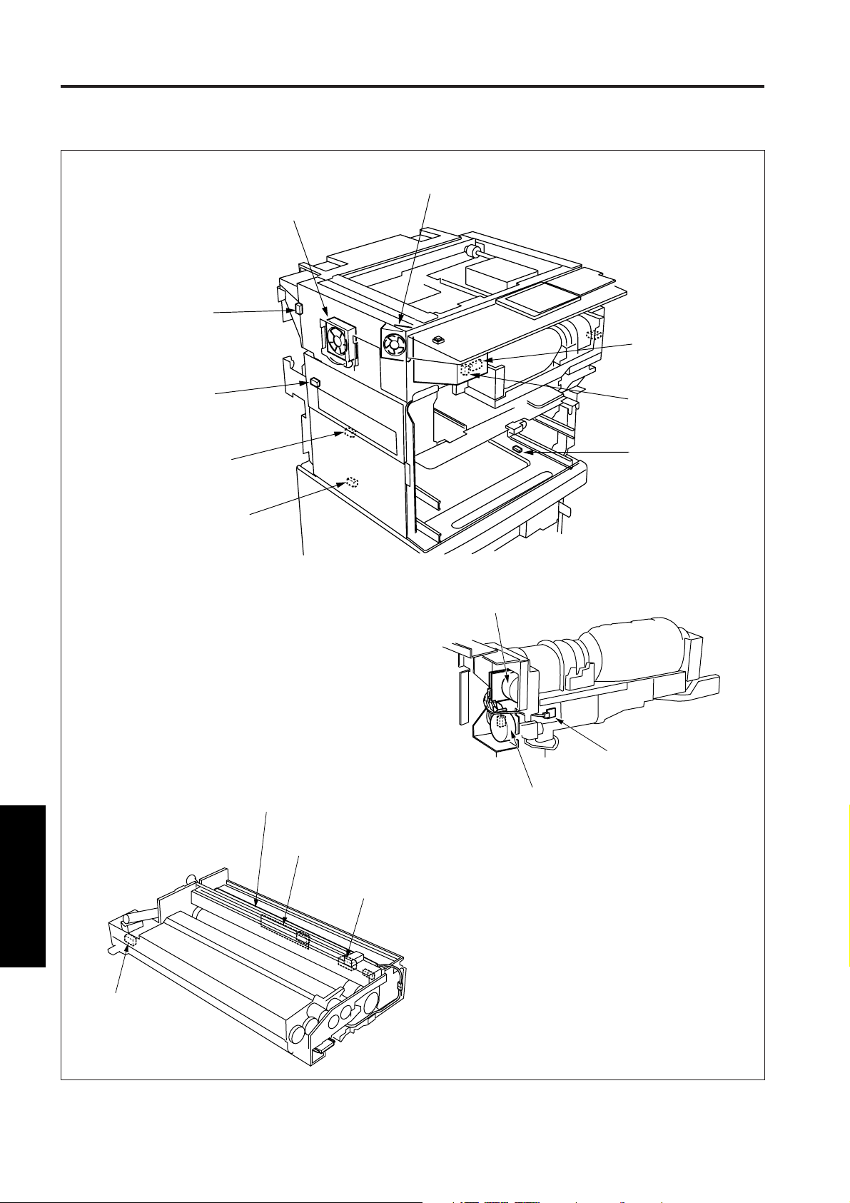
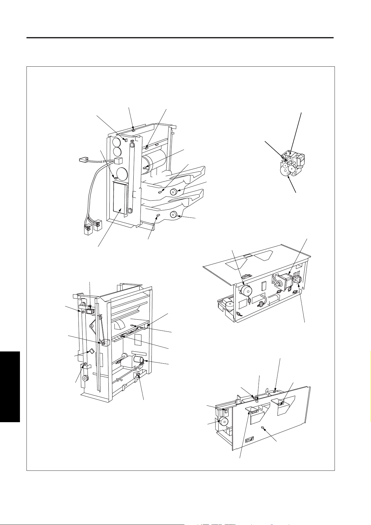
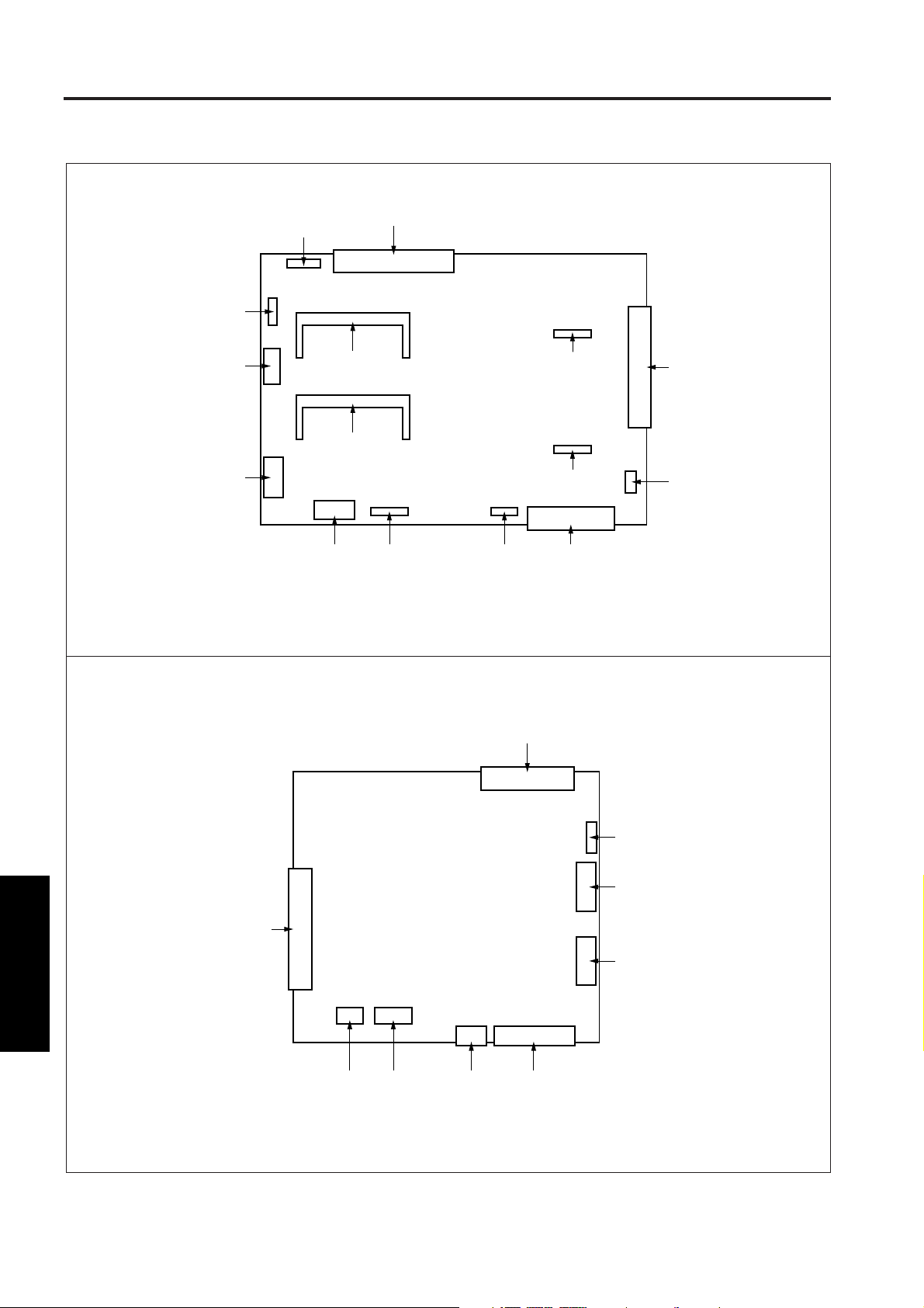
7045 ELECTRICAL PARTS LAYOUT DRAWING
DIAGRAMS
SCDB
Scanner drive board
M3
Developing motor
M6
1st paper feed motor
HV2
High voltage unit 2
SD2
1st paper feed SD
PS31
No paper detect PS
PS32
Upper limit detect PS
MC2
Developing MC
M2
Scanner motor
PFDB
Paper feed detect board
HV1
High voltage unit 1
M8
PRDB
Printer drive board
Tray motor
M4
Drum motor
M1
Main motor
PS1
Paper exit PS
SD5
Gate SD
FM3
Main body cooling fan
M12
Reversal paper exit motor
DCPS1
DC power supply unit 1
LBR
Leak breaker
FM5
DCPS cooling fan
FM4
Conveyance suction fan
LCD
Display board
OB
Operation board
INDEXSB
Index sensor board
ICB
Image control board
ADB
A/D converter board
PRMB
Parameter memory board
PS26
APS sensor 2
PS25
APS sensor 1
OB INV
OB Inverter
PS4
APS timing PS
SW2
Sub power switch
L1
Exposure lamp
L1 INVB
L1 Inverter board
CB
Control board
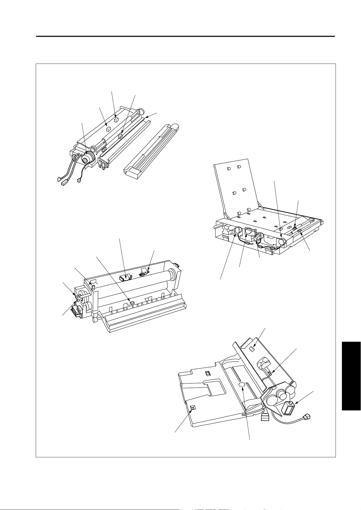
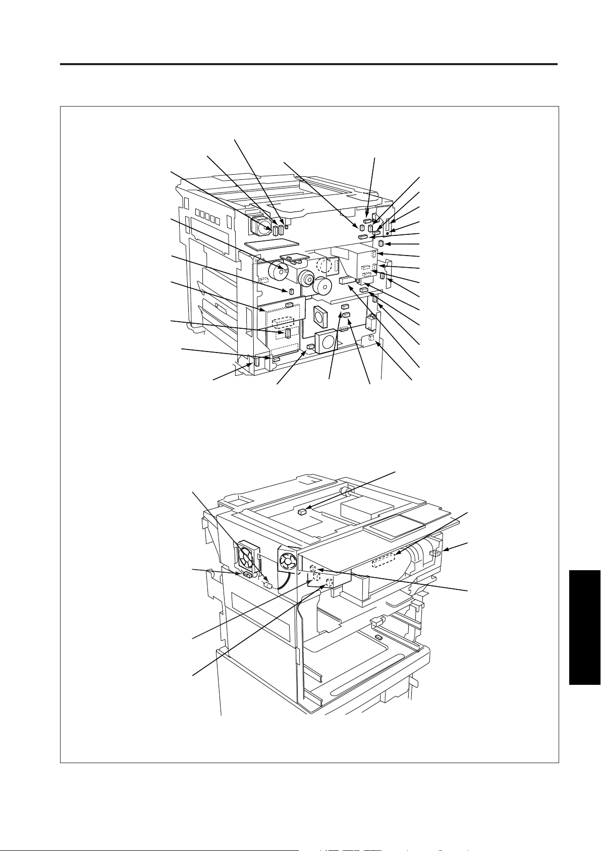
4 DIAGRAM
DCPS2
DC power supply unit 2
PMDB
Polygon motor drive board
PS3
Optics HP PS
5 DIAGRAM
M5
Polygon motor
LDB
Laser drive board
5-1
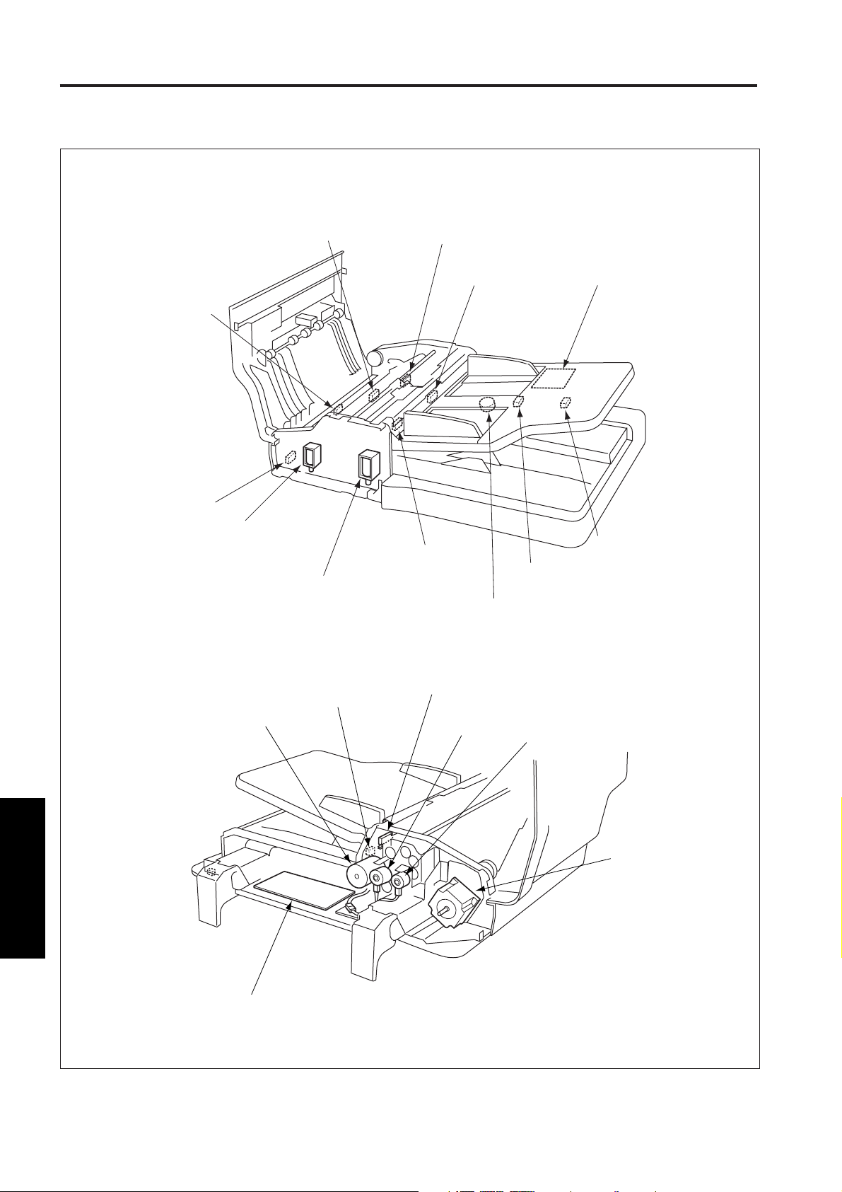
Page 4
DIAGRAMS
SW1
Main power switch
MS2
Inter lock MS2
FM2
Scanner cooling fan 2
FM6
Polygon cooling fan
C(T)
Total counter
MS1
Inter lock MS1
4 DIAGRAM
PS28
Reversal detection PS 1
PS30
Reversal detection PS 2
PCL
Pre-charging lamp
TCSB
Toner control sensor board
PTC
PTC heater
M10
Toner supply motor 1
TLD
Toner level detection sensor
M11
Toner supply motor 2
5 DIAGRAM
TDS
Toner density
detection sensor
SD1
Separation claw SD
5-2
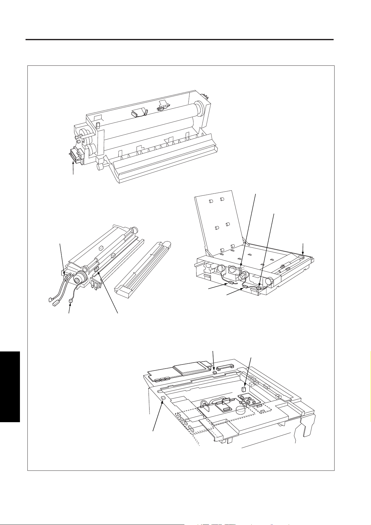
Page 5
DIAGRAMS
HUM1
Humidity sensor
PS17
No feed PS
MC1
Registration MC
PS29
Fixing exit PS
TH2
Fixing temperature sensor 2
L2
Fixing heater lamp 1
PS16
Registration PS
TH1
Fixing temperature sensor 1
TS
Thermostat
TSL
Transfer synchronization lamp
MC503
ADU feed MC
MC501
ADU restart MC
MC502
M501
ADU paper feed motor
ADU loop MC
PS501
ADU no feed PS
PS502
ADU registration PS
L3
Fixing heater lamp 2
PS27
Paper size detection PS (by-pass)
4 DIAGRAM
PS14
Open/close detection PS
PS13
No feed PS (by-pass)
SD4
By-pass SD
5 DIAGRAM
VR1
Paper size detection VR (by-pass)
5-3
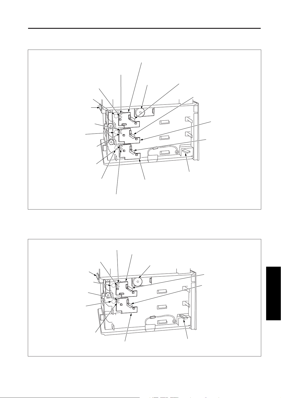
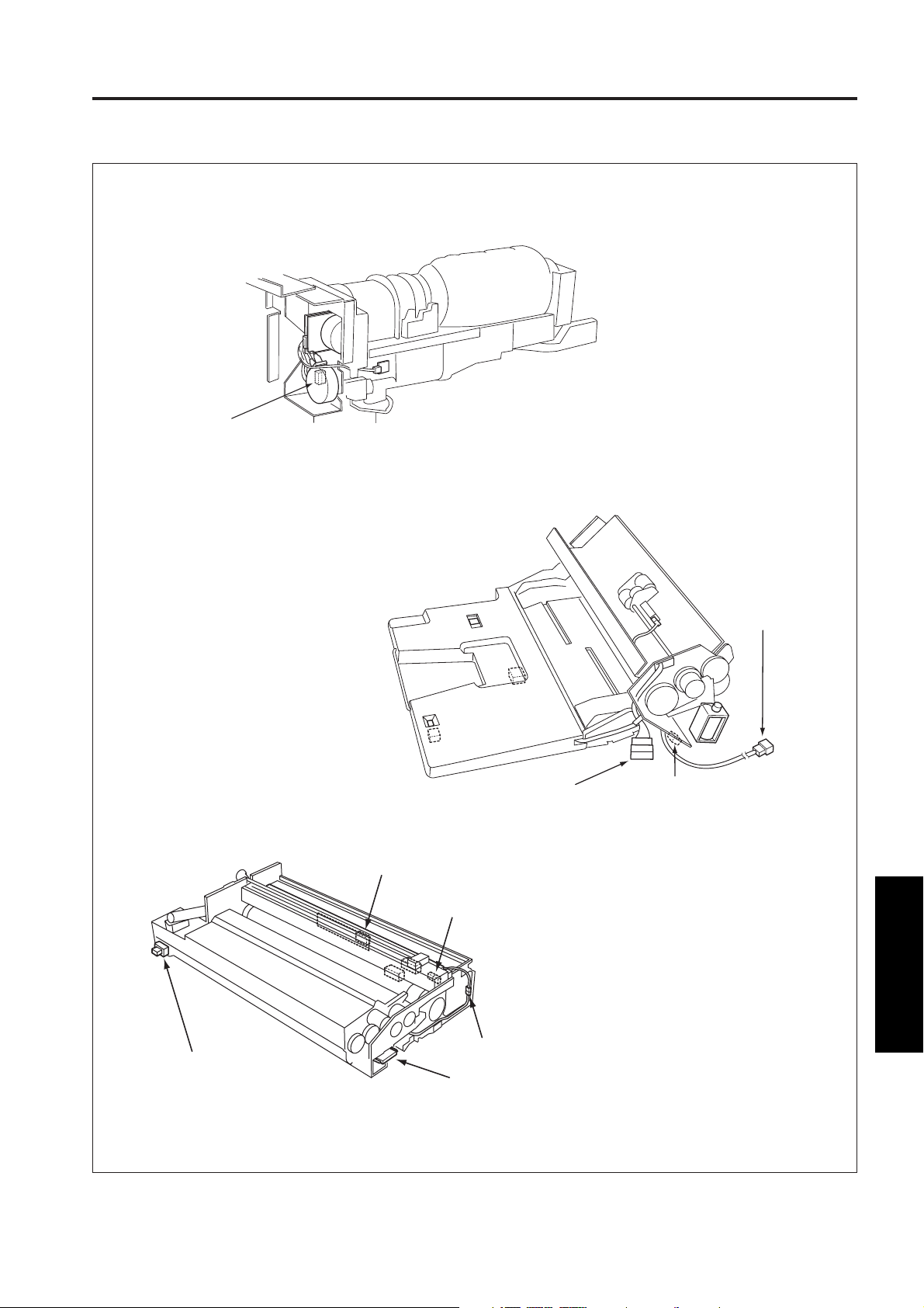
Page 6
DIAGRAMS
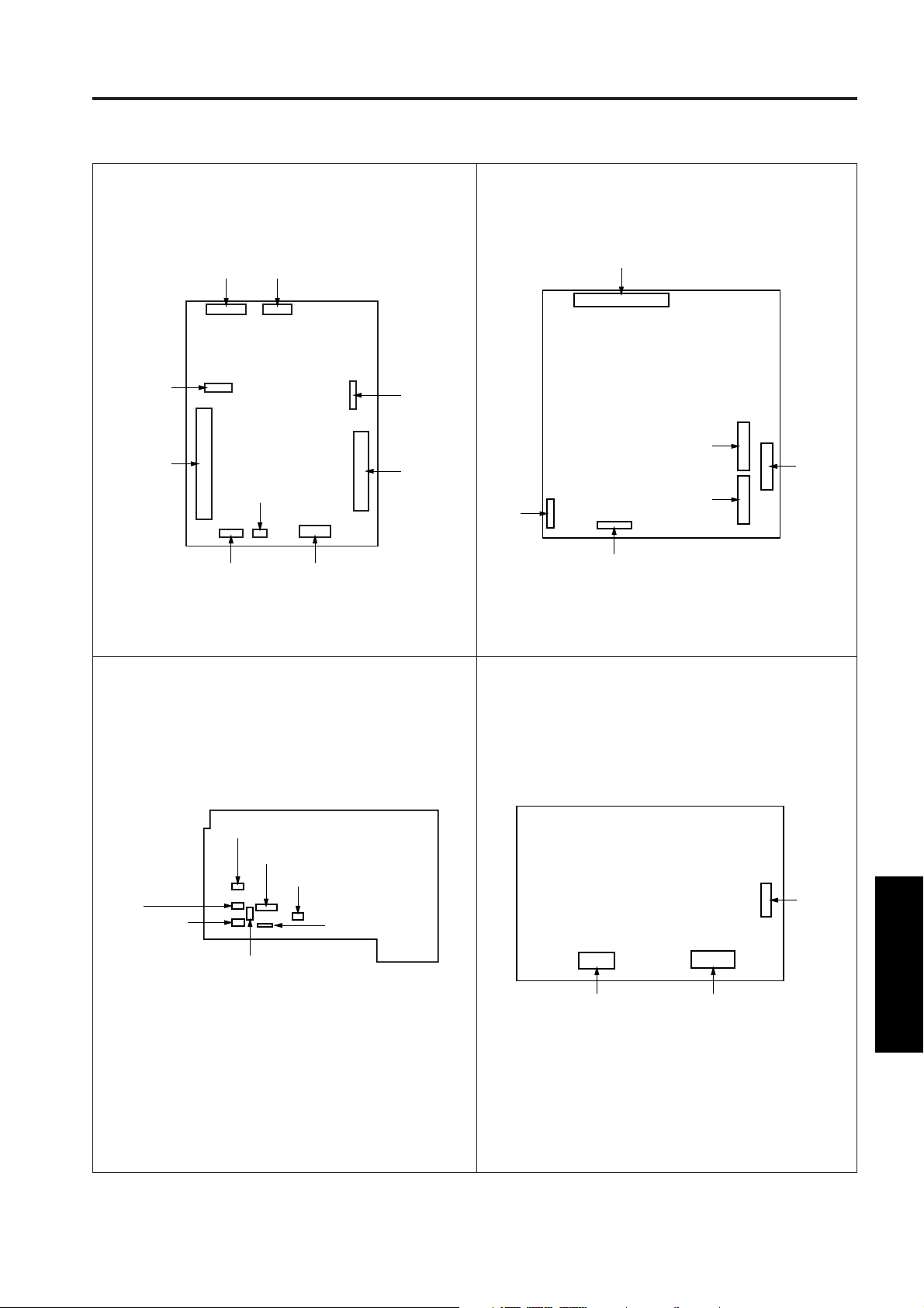
DF-315 ELECTRICAL PARTS LAYOUT DRAWING
PS308
Original feed detect PS
PS301
DF open/close detect PS
SD301
Flapper SD
PS307
Original exit detect PS
PS309
Original reverse detect PS
SD302
Original press SD
PS306
Original registration PS
PS305
No original detect PS
PS303
Original size detect PS2
VR301
Original size detect VR
PTBD
Paper tray board
PS302
Original size detect PS1
5 DIAGRAM
PS304
M302
Original feed motor
DFCB
RADF control board
Motor clock detect PS
MS301
Cover open/close detect MS
CL302
Original feed CL
CL301
Original pick-up CL
M301
Original conveyance motor
5-4
Page 7
DIAGRAMS
DB-208/208A ELECTRICAL PARTS LAYOUT DRAWING
PFUDB (upper)
PFU drive board (U)
PS402
PS403
Upper limit detect PS (U)
SD401
Paper feed SD (PFU) (U)
PS401
Paper feed detect PS
PS404
No paper detect PS (M)
(DB-208 only)
SD402
Paper feed SD (M)
(DB-208 only)
PS405
Upper limit detect PS (M)
(DB-208 only)
PS406
No paper detect PS (L)
(DB-208 only)
SD403
Paper feed SD (L)
(DB-208 only)
No paper detect PS (U)
M401
Paper feed motor
PFUDB (L)
PFU drive board (L) (DB-208 only)
PS407
Upper limit detect PS (L) (DB-208 only)
M402
Up/down motor (U)
M403
Up/down motor (M) (DB-208 only)
PFUDB (M)
PFU drive board (M)
(DB-208 only)
M404
Up/down motor (L)
(DB-208 only)
PTC
PTC heater
DB-608 ELECTRICAL PARTS LAYOUT DRAWING
PS402
No paper detect PS (PFU)
PS403
Upper limit detect PS (PFU)
PS401
Paper feed detect PS
SD401
Paper feed SD (PFU)
PS404
No paper detect PS (LCT)
SD402
Paper feed SD (LCT)
PS405
Upper limit detect PS (LCT)
PFUDB (PFU)
PFU drive board (PFU)
M401
Paper feed motor
PFUDB (LCT)
PFU drive board (LCT)
M402
Up/down motor (PFU)
M403
Up/down motor (LCT)
PTC
PTC heater
5 DIAGRAM
5-5
Page 8
DIAGRAMS
FS-109 ELECTRICAL PARTS LAYOUT DRAWING
PS819
PS803
MS802
Up-down MS (upper)
PS801
Drum position detect PS
Tray 1 paper exit detect PS
FNSCB
FNS control board
PS802
Drum entrance PS
PS809
Tray 3 full-stack detect PS
PS817
Stapler HP (front) PS
PS820
Stapler HP (rear) PS
PS804
Paper through detect PS
PS807
Tray 2 full-stack detect PS
M810
Tray 2 motor
M811
Tray 3 motor
M806
Stapler movement motor
No-staple (front) (lead edge) PS
PS822
No-staple (rear) (lead edge) PS
PS818
No-staple (front) PS
PS821
No-staple (rear) PS
M805
Paper exit motor
PS805
Tray upper limit
PS
M801
Conveyance
motor
MS803
Up-down MS (lower)
PS806
Tray lower limit PS
5 DIAGRAM
SD801
Gate SD
MS801
Inter lock MS
M809 Alignment motor (front)
M807
Conveyance drum
motor
SD802
Shutter SD
MS804
Stapler safety MS
M804
Tray up/down motor
PS812
Stapler no paper
PS815
Alignment motor
(front) HP PS
PS
PS813
Paper exit motor
HP PS
M803
Stapler motor (front)
M808
Alignment motor (rear)
PS816
Alignment motor (rear) HP PS
M802
Stapler motor (rear)
PS814
Stapler unit HP PS
5-6
Page 9
7045 CONNECTOR LAYOUT DRAWING
84 (BK: 3 PIN)
100 (BK: 8 PIN)
87 (W: 2 PIN)
86 (BK: 2 PIN)
152 (BK: 24 PIN)
399 (W: 2 PIN)
100A (BK: 7 PIN)
82 (W: 6 PIN)
85 (BK: 3 PIN)
DIAGRAMS
204 (W: 11 PIN)
205 (W: 2 PIN)
203 (BK: 25 PIN)
509 (BK: 2 PIN)
83 (BK: 8 PIN)
67 (BK: 2 PIN)
141 (W: 2 PIN)
140 (W: 6 PIN)
58 (BK: 4 PIN)
400 (GY: 16 PIN)
145 (W: 3 PIN)
142 (W: 3 PIN)
398 (W: 2 PIN)
300 (GY: 16 PIN)
97 (W: 3 PIN)
98 (BK: 4 PIN)
59 (W: 6 PIN)
57(W: 3 PIN)
392
(W: 3 PIN)
391
(W: 3 PIN)
156 (BK: 3 PIN)
390 (B: 16 PIN)
394 (W: 2 PIN)
92 (W: 6 PIN)
202
(BK: 36 PIN)
79
(BK: 9 PIN)
395
(BK: 2 PIN)
56 (W: 2 PIN)
5 DIAGRAM
5-7
Page 10
DIAGRAMS
390
(B: 16 PIN)
160 (W: 12 PIN)
166 (BK: 2 PIN)
(W: 8 PIN)
5 DIAGRAM
66
86
(BK: 2 PIN)
152 (BK: 24 PIN)
168 (BK: 2 PIN)
167 (BK: 2 PIN)
61
(BK: 2 PIN)
214 (W: 13 PIN)
59 (W: 6 PIN)
55 (W: 6 PIN)
5-8
Page 11
79 (BK: 9 PIN)
DIAGRAMS
65 (BK: 5 PIN)
64 (W: 7 PIN)
63 (BK: 2 PIN)
62 (BK: 2 PIN)
60 (BK: 20 PIN)
80 (BK: 8 PIN)
81 (BK: 5 PIN)
88 (W: 2 PIN)
5 DIAGRAM
5-9
Page 12
DIAGRAMS
Control Board
CN07
(6 pin)
CN01
(4 pin)
CN02
(24 pin)
CN505
(11 pin)
CN503
(144 pin)
CN504
(144 pin)
CN200
(22 pin)
CN500
(100 pin)
CN05
(12 pin)
CN06
(5 pin)
CN03
(20 pin)
CN04
(24 pin)
CN801
(22 pin)
CN10
(100 pin)
CN803
(6 pin)
Image control board
5 DIAGRAM
CN10
(100 pin)
CN17
(10 pin)
CN16
(24 pin)
CN10
(20 pin)
CN11
(80 pin)
CN14
(68 pin)
CN37
(8 pin)
CN12
(22 pin)
CN13
(24 pin)
5-10
Page 13
DIAGRAMS
Printer drive board
CN40
(15 pin)
CN31
(10 pin)
CN32
(60 pin)
CN36
(10 pin)
CN41
(11 pin)
CN35
(5 pin)
CN150
(26 pin)
CN30
(7 pin)
CN33
(50 pin)
Scanner drive board
CN23
(6 pin)
CN11
(80 pin)
CN20
(8 pin)
CN21
(22 pin)
CN24
(26 pin)
CN22
(28 pin)
DC power supply unit 1 DC power supply unit 2
FAN1
(3 pin)
CN387
(12 pin)
CN389
(10 pin)
CN380
(6 pin)
CN381
(7 pin)
CN386
(8 pin)
CN388
(14 pin)
CN1
(4 pin)
CN2
(5 pin)
CN3
(5 pin)
5 DIAGRAM
5-11
Page 14

DIAGRAMS
Polygon motor drive board
CN45
(11 pin)
CN44
(5 pin)
Paper feed detect board
CN317
High voltage unit 1 High voltage unit 2
(3 pin)
CN38
(5 pin)
CN318
(3 pin)
CN316
(13 pin)
CN47
(6 pin)
5 DIAGRAM
CN213
(14 pin)
(14 pin)
CN216
CN217
(5 pin)
CN211
(12 pin)
CN210
(13 pin)
CN48
(4 pin)
Parameter memory boardOperation board
CN1
(20 pin)
CN49
(10 pin)
CN2
(24 pin)
5-12
Page 15

DIAGRAMS
Index sensor board
CN9
(5 pin)
Toner control sensor board
CN64
(7 pin)
L1 Inverter board
CN28
(3 pin)
Laser drive board
CN8
(12 pin)
CN29
(4 pin)
A/D converter board
CN8
(12 pin)
5-13
OB inverter
CN71
(3 pin)
CN77
(4 pin)
5 DIAGRAM
Page 16

DIAGRAMS
DF-315 CONNECTOR LAYOUT DRAWING
46/47 (W:3 PIN)
10 (W:5 PIN)
51 (W:4 PIN)
33/38 (W:6 PIN)
49/50 (W:4 PIN)
45 (W:3 PIN)
52/53 (W:3 PIN)
55/56 (W:2 PIN)
28 (W:3 PIN)
44 (W:3 PIN)
46/47 (W:3 PIN)
12 (W:3 PIN)
11 (W:6 PIN)
43 (W:3 PIN)
57/58
(W:2 PIN)
40 (W:3 PIN)
41 (W:3 PIN)
54 (W:4 PIN)
30 (BK:8 PIN)
5 DIAGRAM
31 (BK:7 PIN)
34/35 (W:2 PIN)
36 (W:4 PIN)
37 (W:4 PIN)
1 (GY:10 PIN)
5-14
3 (W:10 PIN)
9 (W:7 PIN)
4 (W:4 PIN)
DFCB
10 (W:2 PIN)
5 (W:5 PIN)
6 (W:10 PIN)
7 (W:9 PIN)
2 (W:5 PIN)
8 (W:3 PIN)
11 (W:12 PIN)
Page 17

DB-208/208A CONNECTOR LAYOUT DRAWING
310 (GY:18 PIN)
DIAGRAMS
321 (W:12 PIN)
300 (GY:16 PIN)
305 (BK:9 PIN)
312 (W:3 PIN)
313 (W:3 PIN)
317A (W:3 PIN)
317B (W:3 PIN)
311 (GY:24 PIN)
316B (W:13 PIN)
316B (W:3 PIN)
306 (BK:8 PIN)
DB-608 CONNECTOR LAYOUT DRAWING
312 (W:3 PIN)
316A (W:13 PIN)
318A (W:3 PIN)
320 (W:2 PIN)
312 (W:3 PIN)
313 (W:3 PIN)
317 (W:3 PIN)
310 (GY:18 PIN)
311 (GY:24 PIN)
306 (BK:8 PIN)
321 (W:12 PIN)
312 (W:3 PIN)
316A (W:13 PIN)
318 (W:3 PIN)
320 (W:2 PIN)
5 DIAGRAM
300 (GY:16 PIN)
305 (BK:9 PIN)
5-15
Page 18

DIAGRAMS
FS-109 CONNECTOR LAYOUT DRAWING
757(BK:8 PIN)
730 (W:2 PIN)
756 (BK:8 PIN)
736 (W:3 PIN)
759 (W:3 PIN)
749 (W:9 PIN)
761 (BK:8 PIN)
737 (W:3 PIN)
401 (GY:16 PIN)
750
(W:12 PIN)
753
(W:6 PIN)
734 (W:3 PIN)
754 (W:2 PIN)
721 (W:6 PIN)
733 (W:3 PIN)
726
(BK:2 PIN)
724 (W:6 PIN)
763
(W:3 PIN)
724 (W:6 PIN)
744 (W:3 PIN)
760 (W:3 PIN)
751 (W:3 PIN)
723 (W:6 PIN)
727 (W:6 PIN)
725 (W:6 PIN)
743 (W:3 PIN)
741 (W:3 PIN)
740 (W:3 PIN)
746 (W:13 PIN)
742 (W:3 PIN)
745 (W:13 PIN)
722
(W:6 PIN)
5 DIAGRAM
729(W:6 PIN)
751 (BK:3 PIN)
728 (W:6 PIN)
752 (W:3 PIN)
(W:10 PIN)
752 (W:3 PIN)
5-16
702 (W:6 PIN)
701
711
(W:2 PIN)
709
(W:2 PIN)
FNSCB
704 (W:28 PIN)
703 (W:24 PIN)706 (W:15 PIN)
713
(GY:30 PIN)
712
(W:15 PIN)
710
(W:3 PIN)
707
(W:24 PIN)
705 (W:24 PIN)
Page 19

JAM CODE LIST
JAM CODE LIST
Classification
By-pass
feed tray
Tray 1
Main body
DB upper
tray
DB middle
tray or LCT
DB lower
DB
tray
Paper feed
conveyance
Others
Paper feed
conveyance
Fixing/
Paper exit/
Main body, ADU and FNS
ADU
Jam
code
J10
J12
J13
J14
J15
J16
J20-1
J20-2
J20-3
J30
J31
J32
J33
Causes
PS16 (registration) is not turned ON
within a certain period after SD4 (bypass paper feed) has been turned ON.
PS17 (no feed) is not turned ON within a
certain period after SD2 (1st paper feed)
has been turned ON.
PS401 (paper feed detect) is not turned
ON within a certain period after SD401
(paper feed (upper)) has been turned
ON.
PS401 (paper feed detect) is not turned
ON within a certain period after SD402
(paper feed (middle)) has been turned
ON.
PS401 (paper feed detect) is not turned
ON within a certain period after SD403
(paper feed (lower)) has been turned
ON.
PS16 (registration) is not turned ON
within a certain period after PS17 (no
Operating
feed) or PS401 (paper feed detect) has
been turned ON.
During copying, the front door or exit
door was opened.
During copying, the main body
conveyance door was opened.
During copying, the FNS was opened.
PS16 (registration) is not turned OFF
within a certain period after MC1
(registration) has been turned ON.
PS29 (fixing exit) is not turned ON within
a certain period after MC1 (registration)
has been turned ON.
PS1 (paper exit) is not turned ON within
a certain period after PS29 (fixing exit)
has been turned ON. (at the straight
eject mode)
PS1 (paper exit) is not turned OFF
within a certain period after it has been
turned ON. (at the straight eject mode)
Operation when jam
occurs
If a copy is being made
when a jam occurs, copy
operation is stopped
after completion of exit
of the copy.
The main body is
stopped immediately.
Jam clearing method
Remove the original
paper from by-pass
tray, then remove the
jammed paper.
Open the main body
conveyance door and
remove the jammed
paper and close it.
Open the tray and
remove the jammed
paper and close it.
Open the DB conveyance door and remove
the jammed paper and
close it.
Open the tray and
remove the jammed
paper and close it.
Open the main body
conveyance door, DB
conveyance door or
front door and remove
the jammed paper and
close it.
Remove the jammed
paper and close it.
Open the front door and
remove the jammed
paper and close it.
Open the exit door and
remove the jammed
paper and close it.
5 DIAGRAM
5-17
Page 20

JAM CODE LIST
Classification
Fixing/
Paper exit/
ADU
Main body, ADU and DB
Others
RADF
RADF
5 DIAGRAM
Jam
code
J34-1
J34-2
J34-3
J34-4
J34-5
J50-1
J50-2
J50-3
J61-0
J61-1
J62-0
J62-1
J62-2
J62-3
J62-4
Causes
PS28 (reversal detection 1) is not turned
ON within a certain period after PS29
(fixing exit) has been turned ON.
PS28 (reversal detection 1) is not turned
OFF within a certain period after it has
been turned ON.
PS1 (paper exit) is not turned ON within
a certain period after M501 (ADU paper
feed) has been turned ON. (when the
paper is reverse ejected.)
PS1 (paper exit) is not turned OFF
within a certain period after it has been
turned ON. (when the paper is reverse
ejected.)
PS30 (reversal detection 2) is not turned
OFF within a certain period after it has
been turned ON.
When PS16 (registration) is turned on,
print requirement signal is not sent
within the certain time.
When the start button is on, S-valid
does not turn on within the certain time.
When the start button is on, MC1
(registration) does not turn on within the
Operating
certain time.
MS301 (cover open/close detect) is OFF
white the RADF is operating.
PS301 (DF open/close detect) was
turned OFF during RADF operation.
PS306 (original registration) is not
turned ON within a certain period after
the original feed has been started.
PS306 (original registration) is not
turned OFF within a certain period after
it has been turned ON.
PS308 (original feed detect) is not
turned ON within a certain period after
the pre-feed of the duplex original front
side (include the simplex original) has
been started.
PS308 (original feed detect) is not
turned ON within a certain period after
the pre-feed of the duplex original back
side has been started.
PS308 (original feed detect) is not
turned OFF within a certain period after
the scanning of the duplex original front
side (include the simplex original) has
been started.
Operation when jam oc-
curs
The main body is stopped
immediately.
RADF is stopped
immediately.
If there is paper during or
after transfer, the main
body is stopped after exit
of the paper.
Jam clearing method
Open the exit door
and remove the
jammed paper and
close it.
Open the front door
and remove the
jammed paper and
close it.
Open the exit door
and remove the
jammed paper and
close it.
Open the main body
conveyance door, DB
conveyance door or
front door and remove
the jammed paper and
close it.
Open the RADF and
remove the jammed
paper and close it.
5-18
Page 21

JAM CODE LIST
Classification
RADF
RADF
Jam
code
J62-5
J63-0
J63-1
J63-2
J63-3
J63-4
J63-5
J63-6
J63-7
J65-1
J65-2
J65-4
J65-8
Causes
PS308 (original feed detect) is not
turned OFF within a certain period after
the scanning of the duplex original back
side has been started.
PS307 (original exit detect) is not
turned ON within a certain period after
the scanning of the simplex original has
been started.
PS307 (original exit detect) is not
turned ON within a certain period after
the scanning of the duplex original back
side has been started.
At the simplex original is exited, PS307
(original exit detect) is not turned OFF
within a certain period after it has been
turned ON.
At the duplex original is exited, PS307
(original exit detect) is not turned OFF
within a certain period after it has been
Operating
turned ON.
PS309 (original reverse detect) is not
turned ON within a certain period after
the scanning of the duplex original front
side has been started.
PS309 (original reverse detect) is not
turned ON within a certain period after
the reverse feed has been started.
At the start of the duplex original front
side scanning, PS309 (original reverse
detect) is not turned OFF within a
certain period after it has been turned
ON.
At the start of the reverse feed, PS309
(original reverse detect) is not turned
OFF within a certain period after it has
been turned ON.
PS306 (original registration) is ON
during idling.
PS308 (original feed detect) is ON
during idling.
PS309 (original reverse detect) is ON
during idling.
Stationary
PS307 (original exit detect) is ON
during idling.
Operation when jam
occurs
RADF is stopped
immediately.
If there is paper during or
after transfer, the main
body is stopped after exit
of the paper.
Jam clearing method
Open the RADF and
remove the jammed
paper and close it.
5 DIAGRAM
5-19
Page 22

JAM CODE LIST
Classification
FNS
FNS
Paper feed
conveyance
Fixing/
Paper exit/
ADU
Main body and ADU
5 DIAGRAM
Jam
code
J72-1
J72-4
J72-10
J72-11
J72-12
J72-13
J72-14
J72-15
J72-16
J72-21
J72-22
J80
J81
J82
J90
J91
J92
J93
J97-1
J100
Causes
PS802 (drum entrance) is ON during
idling.
PS803 (tray 1 paper exit detect) is ON
Staitionary
during idling.
PS803 (tray 1 paper exit detect) is not
turned ON within a certain period after
PS1 (paper exit) has been turned ON.
PS803 (tray 1 paper exit detect) is not
turned OFF within a certain period after
it has been turned ON.
PS802 (drum entrance) is not turned
ON within a certain period after PS1
(paper exit) has been turned ON.
PS802 (drum entrance) is not turned
OFF within a certain period after it has
been turned ON.
PS804 (paper through detect) is not
turned ON within a certain period after
Operating
PS802 (drum entrance) has been
turned ON.
PS804 (paper through detect) is not
turned OFF within a certain period after
it has been turned ON.
Paper detect sensor of the stapler unit
is not turned ON within a certain period
after M805 (paper exit) has been turned
ON.
Stapler (front) staple jam.
Stapler (rear) staple jam.
PS17 (no feed) is ON during idling.
PS16 (registration) is ON during idling.
PS401 (paper feed detect) is ON during
idling.
PS29 (fixing exit) is ON during idling.
Staitionary
PS1 (paper exit) is ON during idling.
PS28 (reverse detect 1) is ON during
idling.
PS30 (reverse detect 2) is ON during
idling.
PS501 (ADU no feed) is not turned ON
within a certain period after M501 (ADU
paper feed) has been turned ON.
Operating
PS502 (ADU registration) is ON during
idling.
Operation when jam oc-
curs
FNS and main body are
stoped immediately.
The main body are stoped
immediately.
Jam clearing method
Remove the jammed
paper of the FNS and
main body.
Open the main body
conveyance door, DB
conveyance door or
front door and remove
the jammed paper and
close it.
Open the exit door
and remove the
jammed paper and
close it.
Stationary
5-20
Page 23

ERROR CODE LIST
ERROR CODE LIST
Classification
Communication
abnormality
Paper feed
lifting
abnormality
High
voltage
power
supply
abnormality
Warning
code
F10-1
F10-2
F10-3
F18-2
F18-3
F18-4
F18-5
F28-1
F28-2
F28-3
Causes
Serial communication between the
PRDB (printer drive board) and
ICB (image control board) is discontinued.
The answer to the A/D
conversion is not replied two
times consecutively.
DB communication abnormality
signal is detected.
PS32 (upper limit) on the PFDB
(paper feed detect board) is not
turned ON within 26 seconds
from ON of M8 (tray).
PS403 (upper limit detect
(upper)) is not turned ON within
26 seconds from ON of M402
(up/down (upper)).
PS405 (upper limit detect
(middle)) is not turned ON within
26 seconds from ON of M403
(up/down (middle)).
PS407 (upper limit detect
(lower)) is not turned ON within
26 seconds from ON of M404
(up/down (lower)).
When charging output is judged
to be abnormal discharge.
When transfer output is judged to
be an abnormal discharge.
When separation output is
judged to be an abnormal
discharge.
Operation in case of
warning occurrence
The machine stops
immediately, and main relay
and 24VDC are turned OFF.
If a copy being made when
an error occurs, the machine
stops immediately after
completion of exit of the
copy, and main relay and
24VDC are turned OFF.
The machine stops
immediately, and main relay
and 24VDC are turned OFF.
Estimated abnormal parts
PRDB (printer drive board)
ICB (image control board)
SCDB (scanner drive board)
PRDB (printer drive board)
ICB (image control board)
SCDB (scanner drive board)
PFDB (paper feed detect board)
PRDB (printer drive board)
SCDB (scanner drive board)
PFDB (paper feed detect board)
M8 (tray)
M402(up/down (U))
M403(up/down (M))
M404 (up/down (L))
PS32 (upper limit)
PS403 (upper limit detect (U))
PS405 (upper limit detect (M))
PS407 (upper limit detect (L))
PRDB (printer drive board)
HV1 (high voltage unit 1)
Charging corona unit
PRDB (printer drive board)
HV2 (high voltage unit 2)
Transfer corona unit
PRDB (printer drive board)
HV2 (high voltage unit 2)
Separation corona unit
5-21
5 DIAGRAM
Page 24

ERROR CODE LIST
Classification
Fixing high
temperature
abnormality
Fixing low
temperature
Fixing sensor
abnormality
(open circuit)
Scanner
abnormality
5 DIAGRAM
Warning
code
F34-1
F34-2
F34-3
F34-4
F35-1
F35-2
F36-1
F36-2
F40-1
F41-1
Causes
TH1 (fixing temperature 1) detecting temperature (fixing temperature) exceeds approx. 225˚C. (Fixing high temperature abnormality
detection software operates.)
TH1 (fixing temperature 1) detecting temperature (fixing temperature) exceeds approx. 235˚C. (Fixing high temperature abnormality
detection circuit operates.)
TH2 (fixing temperature 2) detecting temperature (fixing temperature) exceeds approx. 235˚C. (Fixing high temperature abnormality
detection software operates.)
TH2 (fixing temperature 2) detecting temperature (fixing temperature) exceeds approx. 250˚C. (Fixing high temperature abnormality
detection circuit operates.)
Warm-up is not completed within
180 seconds from the start of the
warm-up. (Fixing low temperature
abnormality detection software operates.)
After completion of warm-up, fixing
temperature is lower than -30°C.
(Fixing law temperature abnormality software operates.)
Fixing temperature is not reached
30°C within 50 seconds from the
start of the warm-up. (Fixing senser
open circuit detection circuit operates.)
TH2 (fixing temperature 2) is broken (open circuit). (Fixing sensor
open circuit detection circuit operates.)
The errror of SRGA is detected.
At the start of optics initial search or
reverse scanning, PS3 (optics HP)
is not turned ON within a certain
period.
Operation in case of
warning occurrence
The machine stops
immediately, and main relay
and 24VDC are turned OFF.
Set to “1” the bit 1 in SW3.
Scanner stops immediately
and 24VDC is turned OFF.
Estimated abnormal parts
PRDB (printer drive board)
DCPS1 (DC power supply1)
TH1 (fixing temperature 1)
TH2 (fixing temperature 2)
L2 (fixing heater lamp 1)
L3 (fixing heater lamp 2)
ICB (image control board)
ICB (image control board)
SCDB (scanner drive board)
PS3 (optics HP)
5-22
Page 25

ERROR CODE LIST
Classification
Image
processing
abnormality
Motor
abnormality
Fan
abnormality
Warning
code
F46-1
F46-8
F46-10
F46-11
F49-2
F49-4
F49-6
F51-2
F51-3
F51-4
F51-5
F51-6
F51-7
F52-1
F52-2
F52-3
F52-4
F52-5
F52-6
Causes
The monitor value of the laser
light amount is low.
Index cycle differs from the
expectation.
AOC counter overflow
AGC counter overflow
LDB (laser diode board)
connection abnormality
INDEXSB (index sensor board)
connection abnormality
ADB (A/D converter board)
connection abnormality
Speed abnormality in the M1
(main)
Speed abnormality in the M10
(toner supply 1)
Speed abnormality in the M3
(developing)
Speed abnormality in the M4
(drum)
Speed abnormality in the M5
(polygon)
Speed abnormality in the M501
(ADU paper feed)
Locking abnormality in the FM3
(main body cooling).
Locking abnormality in the FM4
(conveyance suction).
Locking abnormality in the M5
(polygon).
Locking abnormality in the FM2
(scanner cooling).
IP-431 cooling fan locking
abnormality (printer kit)
IP-431 CPU cooling fan locking
abnormality .
Operation in case of
warning occurrence
The machine stops
immediately, and main relay
and 24VDC are turned OFF.
Scanner stops immediately.
The machine stops
immediately, and main relay
and 24VDC are turned OFF.
Scanner stops immediately.
The machine stops
immediately, and main relay
and 24VDC are turned OFF.
If a copy being made whenan
error occurs, the machine
stops immediately after
completion of exit of the
copy, and main relay and
24VDC are turned OFF.
The machine stops
immediately, and main relay
and 24VDC are turned OFF.
Estimated abnormal parts
ICB (image control board)
LDB (laser drive board)
ICB (image control board)
INDEXSB (index sensor board)
M5 (polygon)
ICB (image control board)
ADB (A/D converter board)
L1 INVB (L1 inverter board)
DCPS1 (DC power supply 1)
L1 (exposure lamp)
ICB (image control board)
LDB (laser drive board)
INDEXSB (index sensor board)
ICB (image control board)
ICB (image control board)
ADB (A/D converter board)
PRDB (printer drive board)
M1 (main)
PRDB (printer drive board)
M10 (toner supply 1)
PRDB (printer drive board)
M3 (developing)
PRDB (printer drive board)
M4 (drum)
ICB (image control board)
SCDB (scanner drive board)
M5 (polygon)
PRDB (printer drive board)
M501 (ADU paer feed)
PRDB (printer drive board)
FM3 (main body cooling)
PRDB (printer drive board)
FM4 (conveyance suction)
PRDB (printer drive board)
FM5 (polygon)
ICB (Image control board)
SCDB (scanner drive board)
FM2 (scanner cooling)
IP-431cooling fan
IP-431 CPU fan
5 DIAGRAM
5-23
Page 26

ERROR CODE LIST
Classification
Image
processing
communication
abnormality
Operation
unit
abnormality
Control
abnormality
RADF
abnormality
Warning
code
E56-01
E56-02
E56-03
E56-04
E56-05
E56-06
E56-07
E56-08
E56-09
E56-10
F56-11
F60-1
F60-11
Causes
When the SW2 (sub power) is
turned ON, the answer from the ICB
(Image control board) is not replied
to the CB (control board) within 10
seconds.
The CB (control board) is not
detected the process ready signal
60 seconds or more during idling.
The CB (control board) is not
detected the scanner ready
signal 60 seconds or more during
idling.
The CB (control board) is not
detected the finisher ready signal
60 seconds or more during idling.
The CB (control board) is not
detected the original size detect
signal within a certain period
during the platen copy operation.
Memory access abnormality is
occurred at the start of copy
process.
Control abnormality is occurred
at the panel manager.
Miss matching of the display data.
Display data abnormality.
Operation communication
abnormality.
The machine type of the software
version is different from that of
the image processing control
program.
RADF communication
abnormality.
RADF flash ROM abnormality.
Operation in case of
warning occurrence
The machine stops
immediately.
RADF can not be used.
The machine stops
immediately.
Estimated abnormal parts
CB (control borad)
ICB (image control board)
PRDB (printer drive board)
SCDB (scanner drive board)
CB (control borad)
ICB (image control board)
SCDB (scanner drive board)
FNS
CB (control borad)
ICB (image control board)
SCDB (scanner drive board)
CB (control borad)
OB (operation board)
LCD (display board)
ICB program
ICB (image control board)
SCDB (scanner drive board)
RADF
DFCB (RADF control borad)
RADF program
5 DIAGRAM
F67-1
F67-2
F67-3
F67-4
PS306 (original registration),
PS308 (original feed detect),
PS309 (original reverse detect)
adjustment faulty.
PS304 (motor clock detect) is not
detected clock pulse, when M301
(original conveyance) is turned
ON.
Writing and reading abnormality of
the nonvolatile memory (NVRAM).
Other abnormality
(RADF abnormality other than
F67-1 to 3).
RADF can not be used.
5-24
ICB (image control board)
SCDB (scanner drive board)
RADF
Page 27

ERROR CODE LIST
Classification
FNS
abnormality
FNS flash
ROM
abnormality
Warning
code
F70-1
F77-1
F77-2
F77-3
F77-4
F77-5
F77-6
F77-7
F77-8
F77-9
F77-10
F77-11
Causes
FNS communication abnormality
PS805 (tray upper limit) is not
turned ON within 8 seconds from
ON of M804 (up-down (upper)).
Or the MS802 (up-down (upper))
is turned OFF.
PS806 (tray lower limit detect) is
not turned ON within 8 seconds
from ON of M804 (up-down
(upper)).
PS801 (drum position) is not
turned ON within 4 seconds from
ON of M807 (conveyance drum ).
At the forward rotation, PS815
(alignment motor HP (front)) is
not turned OFF within 250 m
seconds from ON of M809
(alignment (front)).
At the reverse rotation, PS815
(alignment motor HP (front)) in
not turned ON within 2 seconds
from ON of M809 (alignment
(front)).
At the forward rotation, PS816
(alignment motor HP (rear) ) is not
turned OFF within 250 m seconds
from ON of M808 (alignment (rear)).
At the reverse rotation, PS816
(alignment motor HP (rear)) in
not turned ON within 2 seconds
from ON of M808 (alignment
(rear)).
At the forward rotation, PS814
(stapler unit HP) is not turned
OFF within 400 milliseconds from
ON of M806 (stapler movement).
At the reverse rotation, PS814
(stapler unit HP) is not turned ON
within 4 seconds from ON of
M806 (stapler movement).
PS813 (paper exit motor HP) is
not turned ON within 1.5 seconds
from ON of M805 (paper exit).
FNS flash ROM abnormality.
Operation in case of
warning occurrence
The machine stops
immediately.
The machine stops
immediately, and main relay
and 24VDC are turned OFF.
The machine stops
immediately.
Estimated abnormal parts
ICB (image control board)
SCDB (scanner drive board)
FNSCB (FNS control board)
FNSCB (FNS control board)
M804 (tray up/down)
MS802 (up/down (upper))
MS803 (up/down (lower))
FNSCB (FNS control board)
M807 (conveyance drum drive)
FNSCB (FNS control board)
M809 (alignment (front))
FNSCB (FNS control board)
M808 (alignment (rear))
FNSCB (FNS control board)
M806 (stapler movement)
FNSCB (FNS control board)
M805 (paper exit)
FNSCB (FNS control board)
FNS program
5 DIAGRAM
5-25
Page 28

ERROR CODE LIST
Classification
FNS
abnormality
Nonvolatile
memory
(NVRAM)
abnormality
Flash ROM
abnormality
IP-431
abnormality
Image
processing
abnormality
Control
board
communication
abnormality
5 DIAGRAM
Warning
code
F77-21
F77-22
F77-30
F80-1
F80-2
F80-3
F80-4
F80-5
F81-01
F81-02
F81-03
F87-02
F87-03
E88-01
E89-01
E89-02
E89-03
E89-04
E89-05
E89-06
Causes
Stapler HP is not turned ON
within a certain period after M803
(stapler (front)) is ON.
Stapler HP is not turned ON
within a certain period after M802
(stapler (rear)) is ON.
MS802 (up-down (upper)) or
MS803 (up-down (lower)) is
turned OFF.
MS804 (stapler safety) is turned
OFF during stapling.
Function parameter abnormality
is detected.
Factory saved data abnormality
is detected.
Function parameter and factory
saved data abnormality are
detected.
Can not be accessed to the
function parameter.
Can not be accessed to the
factory saved data.
The checksum error is detected on
the flash ROM (on the ICB (image
control board) ).
The machine type of software is
differed between CB (control
board) and ICB (image control
board).
The machine and CB (system) program model type do not match.
When SW1 (main power) is on,
there is no response to initialization
command within 5 minetes.
HDD access abnormality
Image processing abnormality is
detected on the CB (control
board).
Job object pointer abnormality
(The page management object is
not obtained with any causes.)
Memory copy sequence
abnormality.
Through copy sequence
abnormality (Cause can not be
determined.)
Memory scan signal stop is not
completed.
Memory printer signal stop is not
completed.
SW2 (sub power) OFF processing is not completed within a
certain period.
Operation in case of
warning occurrence
The machine stops
immediately, and main relay
and 24VDC are turned OFF.
Copy the factory saved data.
–
The machine stops
immediately.
If a copy being made when an
error occurs, the machine
stops immediately after
completion of exit of the copy,
and main relay and 24VDC
are turned OFF.
The machine stops
immediately.
The machine stops immediately and the all indicator are
gone out on operation panel.
Estimated abnormal parts
FNSCB (FNS control board)
M802 (stapler (front))
FNSCB (FNS control board)
M803 (stapler (rear))
FNSCB (FNS control board)
MS802 (up/down (upper)
MS803 (up/down (lower))
MS804 (stapler safety)
(parameter memory board)
PRMB
ICB (image control board)
ICB program
CB (control board)
ICB (image control board)
CB (system) program
ICB program
CB (control board)
CB (system) program
IP-431 control board
CB (control board)
IP-431 control board
CB (control board)
SCDB (scanner drive board)
CB (control board)
ICB (image control board)
PRDB (printer control board)
SCDB (scanner drive board)
CB (control board)
5-26
Page 29

ERROR CODE LIST
When any one of the following abnormality occurs, the user can disconnect the faulty unit temporarily.
When an error code is displayed, press the AUTO RESET button and turning the SW2 (sub power) OFF/ON according to the LCD
message allows you to use the mchine until you turn the SW2 OFF/ON again.
Warning code
10-3
18-2
18-3
18-4
18-5
51-7
60-0, 67-1 to 3
70-1
77-1 to 7, 77-10, 77-30
77-8 to 9, 77-21, 77-22
87-2, 87-3
Contents
DB communication abnormality
Tray (lower) lifting abnormality
DB tray (upper) lifting abnormality
DB tray (middle) lifting abnormality (LCT)
DB tray (lower) lifting abnormality
ADU feed motor abnormality
RADF abnormality
FNS communication abnormality
FNS tray (tray 2 and 3) abnormality
Stapler abnormality (FNS)
IP-431 communication abnormality
Separation subjects
DB unit (all tray)
Main body lower tray
DB upper tray
DB middle tray, LCT
DB lower tray
ADU
RADF
FNS
Tray 2 and 3 (FNS)
Stapler (FNS)
IP
Remarks
Tray can not be selected.
↑
↑
↑
↑
Duplex mode can not be selected.
RADF can not be used.
FNS can not be used.
Tray 2 and 3 (FNS) can not be used.
Stapler mode can not be selected.
Printer can not be used.
5-27
5 DIAGRAM
Page 30

TIMING CHART
7045 TIMING CHART
(A4, LIFE SIZE, MANUAL DENSITY, TWO COPIES, DB MIDDLE TRAY PAPER FEED)
5 DIAGRAM
5-28
Page 31

TIMING CHART
7045 TIMING CHART
(ADF ORIGINAL, A4, LIFE SIZE, AE, TWO COPIES, TRAY1 PAPER FEED)
5-29
5 DIAGRAM
Page 32

PS29
PS28
PS30
PS501
PS502
MC503
MC502
MC501
M501
M12
Fixing exit PS
Reversal detection PS 1
Reversal detection PS 2
ADU no feed PS
ADU registration PS
ADU feed MC
ADU loop MC
ADU restart MC
ADU paper feed motor
Reversal
paper
exit motor
F
R
630 mm/s
210 mm/s
630 mm/s
Symbol
Item
Time (sec)
012 45
(sec)
3
6
50 ms
200 ms
20 ms
20 ms
586 ms
340 ms
138+a ms
50 ms
200 ms
20 ms
20 ms
586 ms
340 ms
(Paper Lengrth +10) / 210 ms
226 ms
138+a ms
(Paper Lengrth +10) / 210 ms
226 ms
50 ms
200 ms
20 ms
20 ms
586 ms
340 ms
138+a ms
(Paper Lengrth +10) / 210 ms
226 ms
TIMING CHART
ADU TIMING CHART (A4, LIFE SIZE, THREE COPIES)
5 DIAGRAM
5-30
Page 33

DF-315 TIMING CHART
0
1
2
3
4
5
6
7
8
9
10
11
12
(sec)
R
F
0
1
2
3
4
5
6
7
8
9
10
11
12
(sec)
R
F
Start button ON
TIMING CHART
[1] A4, ONE SIDE ORIGINALS, FIVE
SHEETS
[2] A4, DUAL-SIDED ORIGINALS, TWO
SHEETS
5 DIAGRAM
5-31
Page 34

TIMING CHART
110ms
320ms
260ms
110ms
320ms
260ms
110ms
320ms
260ms
110ms
320ms
260ms
70ms
70ms
70ms
10ms
280ms
330ms
10ms
100ms
400ms
60ms
10ms
60ms
10ms
60ms
10ms
280ms
330ms
280ms
330ms
280ms
330ms
0
1
2
3
4
5
6
(sec)
70ms
70ms
200ms
250ms
240ms
190ms
60ms
10ms
70ms
70ms
250ms
210ms
200ms
250ms
200ms
250ms
60ms
10ms
60ms
10ms
110ms
320ms
260ms
110ms
320ms
260ms
110ms
320ms
260ms
110ms
320ms
260ms
110ms
260ms
FS-109 TIMING CHART
[1] A4, SORT MODE, THREE SHEETS,
THREE SETS
[2] A4, THREE SHEETS, TWO PLACES
STAPLING, THREE SETS
5 DIAGRAM
5-32
Page 35

0
1
2
3
4
5
6
7
8
9
(sec)
270ms 280ms
60ms
600ms
650ms
10ms
10ms
10ms
140ms
140ms
140ms
10ms
280ms
60ms
10ms
280ms
60ms
10ms
600ms
650ms
600ms
650ms
TIMING CHART
[3] A3, THREE SHEETS, TWO PLACES STAPLING, THREE SETS
5 DIAGRAM
5-33
Page 36

5 DIAGRAM
Blank page
Page 37

DF-315 OVERALL WIRING DIAGRAM
[How to see the diagram]
1.The signals shown reflect levels present
under normal idling conditions with
the main switch turned ON.
2.Wiring symbols in the figure are as follows.
(1) [Symbol]
(2)
Signal typs are as follows :
Active high
Active low
Analog signal
Pulse signal
(3) RC is ribbon cable.
(4) Signal flow
The solid black circle ( ) among
the connector symbols ( )
indicates the direction of signal flow.
Example)
(5) [Colour code]
BN - Brown B - Blue
R - Red V - Violet
O - Orange GY - Gray
Y - Yellow W - White
GN - Green BK - Black
LB - Light blue P - Pink
Example: Y/GN represents
green yellow striped pattern.
V
V
50-1
Crimp
Connector
Wire(Violet)
Faston
CB
5VDC
PS1
SGND
PS1
Direction of
signal flow
H
L
*
P
CN30-1
CN30-4
CN30-5
CN30-8
CN31-4
CN31-1
CN31-6
CN31-2
CN31-3
CN31-5
CN31-7
CN30-7
CN30-6
CN30-3
DFCB
5 DIAGRAM
CN30-2
MAIN BODY
5-35
Page 38

DB-208/208A OVERALL WIRING DIAGRAM
PTC HEATER
M 401
PFUDB (U)
312-1
312-3
313-1
313-3
300-15
300-2
300-14
300-1
300-3
300-4
300-5 P
300-6
300-7
300-8
300-10
300-9
300-13
300-12
24VDC
M402 DRIVE
24VDC
SD401 DRIVE
5VDC
S.GND
PS402
5VDC
S.GND
PS403
SD401
PS402
PS403
M 402
PFUDB (M)
318A-1
318A-3
317A-1
317A-3
24VDC
M403 DRIVE
24VDC
SD402 DRIVE
5VDC
S.GND
PS404
5VDC
S.GND
PS405
SD402
PS404
PS405
M 403
PFUDB (L)
318B-1
318B-3
317B-1
317B-3
24VDC
M404 DRIVE
24VDC
SD403 DRIVE
5VDC
S.GND
PS406
5VDC
S.GND
PS407
SD403
PS406
PS407
PS401
M 404
UP/DOWN
MOTOR
(L)
PAPER
FEED
SOLENOID
(L)
UP/DOWN
MOTOR
(M)
PAPER
FEED
SOLENOID
(M)
UP/DOWN
MOTOR
(U)
PAPER
FEED
MOTOR
PAPER FEED
DETECT
SENSOR
PAPER
FEED
SOLENOID
(U)
UPPER LIMIT
DETECT
SENSOR
(L)
NO PAPER
DETECT
SENSOR
(L)
UPPER LIMIT
DETECT
SENSOR
(M)
NO PAPER
DETECT
SENSOR
(M)
UPPER LIMIT
DETECT
SENSOR
(U)
NO PAPER
DETECT
SENSOR
(U)
311-B11
311-B12
311-B10
311-B9
311-A4
311-B8
311-B7
311-B6
311-B5
311-A11
311-A12
311-A10
311-A9
311-B3
311-A3
311-A8
311-A7
311-A6
311-A5
PS406
PS407
M404 DRIVE
SD403 DRIVE
SIZE SCN2
SIZE D
SIZE C
SIZE B
SIZE A
PS404
PS405
M403 DRIVE
SD402 DRIVE
SELECT
SIZE SCN1
SIZE D
SIZE C
SIZE B
SIZE A
316B-13
316B-7
316B-10
316B-1
316B-2
316B-3
316B-4
316B-5
316B-6
316B-8
361B-9
316B-11
361B-12
5VDC
S.GND
24VDC
SIZE A
SIZE B
SIZE C
SIZE D
SIZE SCN2
SD403 DRIVE
M404 DRIVE
PS407
PS406
316A-13
316A-7
316A-10
316A-1
316A-2
316A-3
316A-4
316A-5
316A-6
316A-8
361A-9
316A-11
361A-12
5VDC
S.GND
24VDC
SIZE A
SIZE B
SIZE C
SIZE D
SIZE SCN1
SELECT
SD402 DRIVE
M403 DRIVE
PS405
PS404
P.GND
(DCPS1)
P.GND
(DCPS1)
24VDC
(DCPS1)
24VDC
(DCPS1)
5VDC
(SCDB)
S.GND
(SCDB)
DB MTXD
(SCDB)
(SCDB)
DB SRXD
(SCDB)
(SCDB)
(PRDB)
X RESET
(PRDB)
28VDC
(DCPS1)
P.GND
(DCPS1)
310-B4
310-B3
310-A3
310-A2
310-A1
310-B1
310-A6
P 310-A5
P 310-A4
310-A7
P 310-A9
310-A8
DB MACK
DB SRXD
MPS DATA
311-A2
311-B1
311-A1
24VDC
S.GND
5VDC
311-B2 H
312-2
312-3
312-1
PS401
310-B6
310-B8
310-B7
310-B2
310-B9
310-B5
321-3
321-4
321-5
321-10
321-12
321-8
321-2
321-1
M401 CONT
M401 CLK
M401 H/L
24VDC
M401 CW/CCW
P.GND
SW401
SW402
SW403
SW404
SW401
SW402
SW403
SW404
SW401
SW402
SW403
SW404
MAIN BODY
320-2
320-1
PTC
P
R
BK
R
BK
R
BK
R
BK
R
BK
R
BK
P
P
H
H
H
H
H
H
H
H
H
H
H
H
H
H
P
P
O
O
O
O
O
O
O
O
O
O
O
O
O
O
O
O
O
O
O
[How to see the diagram]
1.The signals shown reflect levels present
under normal idling conditions with
the main switch turned ON.
2.Wiring symbols in the figure are as follows.
(1) [Symbol]
(2)
Signal typs are as follows :
Active high
Active low
Analog signal
Pulse signal
(3) RC is ribbon cable.
(4) Signal flow
The solid black circle ( ) among
the connector symbols ( )
indicates the direction of signal flow.
Example)
(5) [Colour code]
BN - Brown B - Blue
R - Red V - Violet
O - Orange GY - Gray
Y - Yellow W - White
GN - Green BK - Black
LB - Light blue P - Pink
Example: Y/GN represents
green yellow striped pattern.
V
V
50-1
Crimp
Connector
Wire(Violet)
Faston
CB
5VDC
PS1
SGND
PS1
Direction of
signal flow
H
L
*
P
DB-208
DB-208A
5 DIAGRAM
5-36
Page 39

DB-608 OVERALL WIRING DIAGRAM
R
BK
R
BK
R
BK
R
BK
PTC
PTC HEATER
320-2
320-1
O
O
O
O
O
O
O
O
O
O
M 401
SW405
SW401
SW402
SW403
SW404
MAIN BODY
PFUDB (PFU)
312-1
312-3
313-1
313-3
300-15
300-2
300-14
300-1
300-3
300-4
300-5 P
300-6
300-7
300-8 P
300-10
300-9
300-13
300-12
24VDC
M402 DRIVE
24VDC
SD401 DRIVE
5VDC
S.GND
PS402
5VDC
S.GND
PS403
SD401
PS402
PS403
M 402
PFUDB (LCT)
318A-1
318A-3
317A-1
317A-3
24VDC
M403 DRIVE
24VDC
SD402 DRIVE
5VDC
S.GND
PS404
5VDC
S.GND
PS405
SD402
PS404
PS405
M 403
PS401
UP/DOWN
MOTOR
(LCT)
PAPER
FEED
SOLENOID
(LCT)
UP/DOWN
MOTOR
(PFU)
PAPER
FEED
MOTOR
PAPER FEED
DETECT
SENSOR
PAPER
FEED
SOLENOID
(PFU)
UPPER LIMIT
DETECT
SENSOR
(LCT)
NO PAPER
DETECT
SENSOR
(LCT)
UPPER LIMIT
DETECT
SENSOR
(PFU)
NO PAPER
DETECT
SENSOR
(PFU)
311-A11
311-A12
311-A10 H
311-A9 H
311-B3
311-A3 P
311-A8
311-A7
311-A6
311-A5
PS404
PS405
M403 DRIVE
SD402 DRIVE
SELECT
SIZE SCN1
SIZE D
SIZE C
SIZE B
SIZE A
316A-13
316A-7
316A-10
316A-1
316A-2
316A-3
316A-4
316A-5
316A-6
316A-8
361A-9
316A-11
361A-12
5VDC
S.GND
24VDC
SIZE A
SIZE B
SIZE C
SIZE D
SIZE SCN1
SELECT
SD402 DRIVE
M403 DRIVE
PS405
PS404
P.GND(DCPS1)
P.GND(DCPS1)
24VDC(DCPS1)
24VDC(DCPS1)
5VDC(SCDB)
S.GND(SCDB)
DK MTXD(SCDB)
(SCDB)
(SCDB)
DB SACK(SCDB)
(PRDB)
X RESET(PRDB)
28VDC(DCPS1)
P.GND(DCPS1)
310-B4
310-B3
310-A3
310-A2
310-A1
310-B1
310-A6
310-A5
310-A4
310-A7
310-A9
310-A8
DB MACK
DB SRXD
MPS DATA
311-A2
311-B1
311-A1
24VDC
S.GND
5VDC
311-B2 H
312-2
312-3
312-1
PS401
310-B6
310-B8
310-B7
310-B2
310-B9
310-B5
321-3
321-4
321-5
321-10
321-12
321-8
321-2
321-1
M401 CONT
M401 CLK
M401 H/L
24VDC
M401 CW/CCW
P.GND
P
H
H
H
H
H
H
P
P
P
[How to see the diagram]
1.The signals shown reflect levels present
under normal idling conditions with
the main switch turned ON.
2.Wiring symbols in the figure are as follows.
(1) [Symbol]
(2)
Signal typs are as follows :
Active high
Active low
Analog signal
Pulse signal
(3) RC is ribbon cable.
(4) Signal flow
The solid black circle ( ) among
the connector symbols ( )
indicates the direction of signal flow.
Example)
(5) [Colour code]
BN - Brown B - Blue
R - Red V - Violet
O - Orange GY - Gray
Y - Yellow W - White
GN - Green BK - Black
LB - Light blue P - Pink
Example: Y/GN represents
green yellow striped pattern.
V
V
50-1
Crimp
Connector
Wire(Violet)
Faston
CB
5VDC
PS1
SGND
PS1
Direction of
signal flow
H
L
*
P
5 DIAGRAM
5-37
Page 40

FS-109 OVERALL WIRING DIAGRAM
[How to see the diagram]
1.The signals shown reflect levels present
under normal idling conditions with
the main switch turned ON.
2.Wiring symbols in the figure are as follows.
(1) [Symbol]
(2)
Signal typs are as follows :
Active high
Active low
Analog signal
Pulse signal
(3) RC is ribbon cable.
(4) Signal flow
The solid black circle ( ) among
the connector symbols ( )
indicates the direction of signal flow.
Example)
V
V
50-1
Crimp
Connector
Wire(Violet)
Faston
CB
5VDC
PS1
SGND
PS1
Direction of
signal flow
H
L
*
P
PAPER THROUGH
DETECTSENSOR
DRUM POSITION
DETECT SENSOR
DRUM ENTRANCE
SENSOR
TRAY 1
PAPER EXIT
DETECT SENSOR
TRAY
UPPER LIMIT
SENSOR
TRAY
LOWER LIMIT
SENSOR
TRAY 3
FULL–STACK
DETECT SENSOR
TRAY 2
FULL–STACK
DETECT SENSOR
STAPLER NO
PAPER SENSOR
PAPER EXIT
MOTOR HP SENSOR
STAPLER UNIT HP SENSOR
ALIGNMENT MOTOR
HP (FRONT) SENSOR
ALIGNMENT MOTOR
(REAR) HP
STAPLER (FRONT)
MOTOR
STAPLER HP (FRONT) SENSOR
NO STAPLE (FRONT) SENSOR
NO STAPLE (FRONT)
(LEAD EDGE) SENSOR
STAPLER (REAR)
MOTOR
STAPLER HP (REAR) SENSOR
NO STAPLE (REAR) SENSOR
NO STAPLE (REAR)
(LEAD EDGE) SENSOR
PAPER EXIT
CN727–4
CN727–2
CN727–5
25314
UL1007#24
UL1007#24
5253545556
CN705–B8 24V
CN705–B7 24V
PPP
CN704–B5 M801 DRVA
CN704–B7 M801 DRVB
CN704–B6 M801 DRVA
PPP
22
MOTOR
M805
CN727–6
CN727–3
UL1007#24
UL1007#24
UL1007#24
CN705–B10 M805 DRVA
CN705–B11 M805 DRVB
CN705–B9 M805 DRVA
CN704–B8 M801 DRVB
CN727–1
6
UL1007#24
57
CN705–B12 M805 DRVB
P
TRAY UP/DOWN
MOTOR
M804
CN726–1
CN726–2
UL1007#24
UL1007#24
23
24
CN707–A8 M804 DRV1
CN707–A9 M804 DRV2
H
H
CN704–B1 24V
CN704–B2 24V
P
1516192021
TRAY 2 MOTOR
M810
CN728–5
CN728–6
CN728–1
CN728–3
18
CN753–12
CN753–11
CN753–10
CN753–9
CN753–1
CN753–2
CN753–3
CN753–4
UL1007#26
UL1007#26
UL1007#26
34789
CN704–A7 M810 DRVA
CN704–A4 24V
CN704–A3 24V
PPP
CN704–B3 24V
CN704–B4 24V
PPP
1718232425
CN728–2
CN728–4
1314151617
CN753–8
CN753–7
CN753–5
CN753–6
UL1007#26
UL1007#26
UL1007#26
10
CN704–A9 M810 DRVB
CN704–A10 M810 DRVB
CN704–A8 M810 DRVA
P
CN704–B9 M807 DRVA
CN704–B10 M807 DRVA
CN704–B12 M807 DRVB
CN704–B11 M807 DRVB
P
26
CN729–5
12
CN753–6
CN753–7
56111213
UL1007#24
UL1007#24
UL1007#24
UL1007#24
UL1007#24
UL1007#24
UL1007#24
UL1007#24
UL1007#24
UL1007#24
UL1007#24
UL1007#24
5 DIAGRAM
25314
CN721–5
CN721–4
CN721–2
6
CN721–3
CN721–6
CN721–1
25314
CN722–2
CN722–5
CN722–6
CN722–4
6
CN722–3
CN722–1
M801
M807
ONVEYANCE MOTOR
CONVEYANCE
DRUM MOTOR
TRAY 3 MOTOR
M811
CN729–6
CN729–1
CN729–3
CN753–5
CN753–4
CN753–3
CN753–8
CN753–9
CN753–10
UL1007#26
UL1007#26
UL1007#26
UL1007#26
CN704–A12 M811 DRVA
CN704–A11 M811 DRVA
CN704–A6 24V
CN704–A5 24V
PPP
CN705–B1 24V
4647484950
UL1007#26
CN762–1
CN763–6
6
CN723–5
CN723–2
CN729–2
CN729–4
7891011
CN753–2
CN753–1
CN753–11
CN753–12
UL1007#26
UL1007#26
14
CN704–A14 M811 DRVB
CN704–A13 M811 DRVB
P
CN705–B2 24V
CN705–B3 M808 DRVA
CN705–B4 M808 DRVA
PPP
UL1007#26
UL1007#26
UL1007#26
CN762–4
CN762–5
CN762–3
CN762–2
CN763–5
CN763–4
CN763–3
CN763–2
CN723–6
CN723–1
CN723–3
CN723–2
CN723–5
CN723–4
CN723–6
CN723–1
M808
ALIGNMENT
MOTOR (REAR)
GATE SOLENOID
SD801
CN730–1
CN730–2
UL1007#26
2
1
CN704–A1 24V
CN705–B5 M808 DRVB
CN705–B6 M808 DRVB
P
51
UL1007#26
UL1007#26
CN762–6
CN763–1
12345
CN723–4
CN723–3
SHUTTER SOLENOID
SD802
CN731–2
CN731–1
1
2
CN748–1
CN748–2CN748–1
CN748–2
UL1007#26
UL1007#26
UL1007#26
27
28
CN704–A2 SD801 DRV
CN704–B14 24V
CN704–B13 SD802 DRV
H
H
CN705–A1 24V
CN705–A2 24V
PPP
3436373839
35
UL1007#26
UL1007#26
CN761–1
CN761–2
CN761–3
CN761–6
CN761–5
CN761–4
456
CN724–1
CN724–6
CN724–5
CN724–2
CN724–1
CN724–6
CN760–1
543
CN763–3
CN763–1
UL1007#26
424140
CN703–A12 VCC
CN705–A3 M809 DRVA
CN705–A4 M809 DRVA
CN705–A5 M809 DRVB
P
UL1007#26
UL1007#26
UL1007#26
CN761–4
CN761–5
CN761–6
CN761–3
CN761–2
CN761–1
132
CN724–4
CN724–2
CN724–3
CN724–4
CN724–5
CN724–3
M809
ALIGNMENT
MOTOR (FRONT)
PS804
CN760–2
CN760–3
CN760–2
CN763–1CN763–3
CN763–2
UL1007#26
UL1007#26
CN703–A11 PS804IN
CN703–A10 GND
CN705–A7 24V
CN705–A6 M809 DRVB
4042434445
UL1007#26
UL1007#26
CN725–6
CN725–1
CN705–A8 24V
CN705–A9 M806 DRVA
CN705–A10 M806 DRVA
PPP
41
UL1007#26
UL1007#26
UL1007#26
CN725–1
CN725–2
CN725–3
CN725–5
CN725–6
CN725–5
CN725–4
CN725–2
M806
STAPLER
MOVEMENT
MOTOR
PS801
CN732–3
CN732–2
CN732–1
UL1007#26
UL1007#26
UL1007#26
484746
CN703–B5 PS801IN
CN703–B4 GND
CN703–B6 VCC
CN705–A12 M806 DRVB
CN705–A11 M806 DRVB
P
UL1007#26
UL1007#26
CN725–4
CN725–3
PS802
CN733–1
CN733–2
CN733–3
UL1007#26
UL1007#26
UL1007#26
454344
CN703–B1 GND
CN703–B2 PS802IN
CN703–B3 VCC
L
T
OU
V
24
CN711–2
2
UL1015#18
CN734–1
CN734–2
UL1007#26
38
39
CN703–A9 VCC
IN
V
24
CN711–1
1
UL1015#18
MS801
INTER LOCK MS
PS803
PS805
CN734–3
CN736–1
CN736–2
CN736–3
UL1007#26
UL1007#26
UL1007#26
UL1007#26
UL1007#26
37
3635343332
CN703–A4 GND
CN703–A5 PS805IN
CN703–A6 VCC
CN703–A8 PS803IN
CN703–A7 GND
L
L
FNSCB
T
OU
V
24
CN710–2
CN754–1
UL1015#18
MS (UPPER)
55
CN755–2
30
UL1007#22
CN754–2
UL1015#18
MS802
UP–DOWN
PS806
CN737–1
CN737–2
CN737–3
UL1007#26
UL1007#26
UL1007#26
UL1007#26
UL1007#26
31
CN703–A1 GND
CN703–A3 VCC
CN703–A2 PS806IN
H
V IN
24
CN710–1
29
UL1007#22
UL1007#22
CN755–1
UL1015#18
UL1015#18
MS803
UP–DOWN
MS (LOWER)
PS809
CN752–1
CN752–2
CN752–3
456
CN750–4
CN750–5
CN750–6
CN750–1
CN750–2
CN750–3
UL1007#26
UL1007#26
UL1007#26
UL1007#26
UL1007#26
545352
CN703–B10 GND
CN703–B11 PS809IN
CN703–B12 VCC
L
V IN
V OUT
24
24
CN709–1
CN709–2
1
2
UL1007#18
UL1015#18
MS804
STAPLER
SAFETY
MS
PS807
CN751–1
CN751–2
CN751–3
123
CN750–1
CN750–2
CN750–3
CN750–4
CN750–5
CN750–6
UL1007#26
UL1007#26
UL1007#26
UL1007#26
UL1007#26
51
50
49
CN703–B8 PS817IN
CN703–B7 GND
CN703–B9 VCC
L
PS812
CN740–1
CN740–2
CN740–3
789
CN749–8
CN749–7
CN759–1 CN749–9
CN749–3
CN749–2
UL1007#26
UL1007#26
UL1007#26
UL1007#26
UL1007#26
151413
CN706–13 GND
CN706–14 PS812IN
CN706–15 VCC
PS813
CN741–1
CN741–2
CN741–3
456
CN749–6
CN749–5
CN749–4
CN749–6
CN749–5
CN749–4
UL1007#26
UL1007#26
UL1007#26
UL1007#26
UL1007#26
12
10
11
CN706–12 VCC
CN706–10 GND
CN706–11 PS813IN
H
PS814
CN742–1
CN742–2
CN742–3
123
CN749–3
CN749–2
CN759–1
CN749–9
CN749–8
CN749–7
UL1007#26
UL1007#26
UL1007#26
UL1007#26
UL1007#26
789
CN706–7 GND
CN706–8 PS814IN
CN706–9 VCC
L
PS815
PS816
CN743–1
CN743–2
CN743–3
CN744–1
CN744–2
CN744–3
789
789
CN759–3
CN759–2
CN758–1
CN759–2
CN759–1
CN758–3
UL1007#26
UL1007#26
UL1007#26
UL1007#26
UL1007#26
456
CN706–2 PS816IN
CN706–3 VCC
CN706–4 GND
H
GND
GND
GND
V
V
S.
5
5
P.
P.
CN701–6
CN701–2
CN701–3
CN701–4
CN701–5
UL1007#24
UL1007#24
UL1007#24
UL1007#24
UL1007#24
CN401–7 P.GND
CN402–5 P.GND
CN402–1 S.GND
CN401–8 5V
CN402–2 5V
CN759–1
CN759–3
UL1007#26
UL1007#26
123
CN706–1 GND
.GND
P
CN701–7
UL1007#24
CN402–3 P.GND
CN758–3
CN758–2
CN758–2
CN758–1
UL1007#26
UL1007#26
UL1007#26
CN706–5 PS815IN
CN706–6 VCC
H
GND
S.
CN701–1
123456789
UL1007#24
CN401–5 S.GND
M803
CN745–6
CN745–3
CN745–1
1234567
CN756–1
CN756–2
CN756–3
16171920212218
UL1007#24
UL1007#24
UL1007#26
CN707–A1 M803 DRV1
CN707–A4 VCC
CN707–A2 M803 DRV2
V
V
V
_TXD
_REQ
24
24
24
M
M
CN701–8
CN701–9
CN701–10
CN702–1
CN702–2
PPPPP
10111213141516
UL1007#24
UL1007#24
UL1007#26
UL1007#26
UL1007#24
CN401–4 M_TxD
CN401–3 M_REQ
CN401–8 24V
CN402–8 24V
CN402–4 24V
PS817
PS818
PS819
CN745–5
CN745–11
CN745–7
CN745–9
8
CN756–4
CN756–5
CN756–6
CN756–7
CN756–8
59
UL1007#26
UL1007#26
UL1007#26
UL1007#26
UL1007#22
CN707–A3 GND
CN707–A7 PS819IN
CN707–A6 PS818IN
CN707–A5 PS817IN
LLL
_RXD
_ACK
_ACK
_REQ
S
M
M
S
CN702–4
CN702–3
CN702–5
CN702–6
P
UL1007#26
UL1007#26
UL1007#26
UL1007#26
CN402–7 S_ACK
CN401–1 S_RxD
CN402–8 S_REQ
CN401–2 M_ACK
CN746–1
1234567
CN757–1
33323029282831
17
UL1015#18
EARTH
CN100 –
MAIN BODY
M802
+5V
CN746–3
CN746–6
CN757–2
CN757–3
UL1007#24
UL1007#24
UL1007#24
CN707–B9 M802 DRV1
CN707–B8 M802 DRV2
CN707–B6 VCC
GND
PS820
PS821
PS822
CN746–9
CN746–7
CN746–11
CN746–5
8
CN757–4
CN757–5
CN757–6
CN757–7
CN757–8
58
UL1007#24UL1007#24
UL1007#24
UL1007#24
UL1007#24
UL1007#22
CN707–B7 GND
CN707–B3 PS822IN
CN707–B4 PS821IN
CN706–B5 PS820IN
LLL
5-38
Page 41

PRINTED IN JAPAN
CN55YF1300
 Loading...