

Page 1

5
DIAGRAMS
5 DIAGRAMS
Page 2
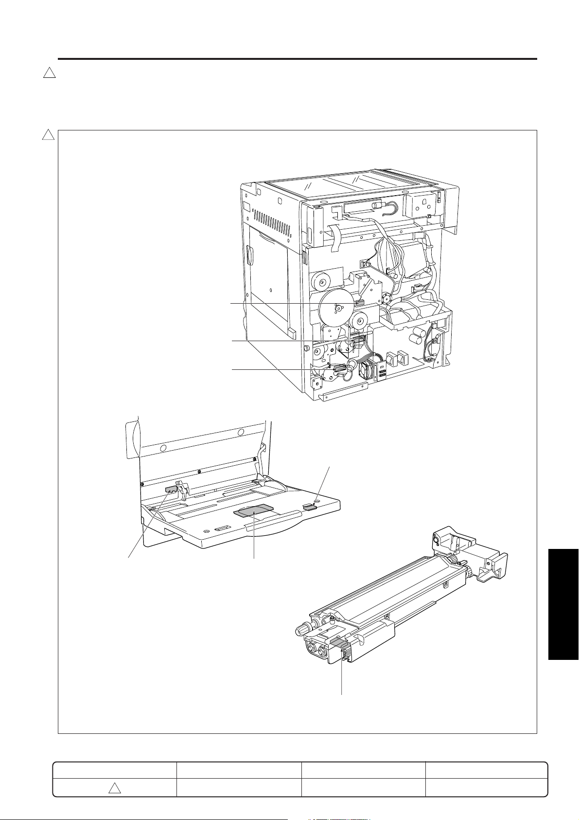
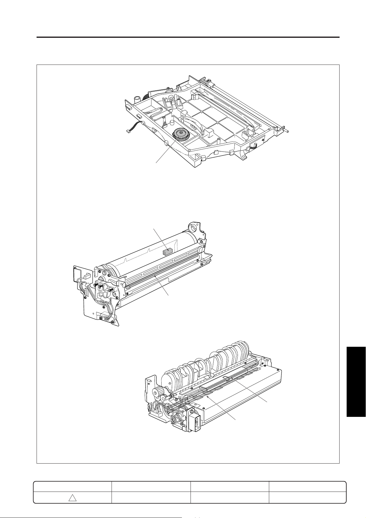
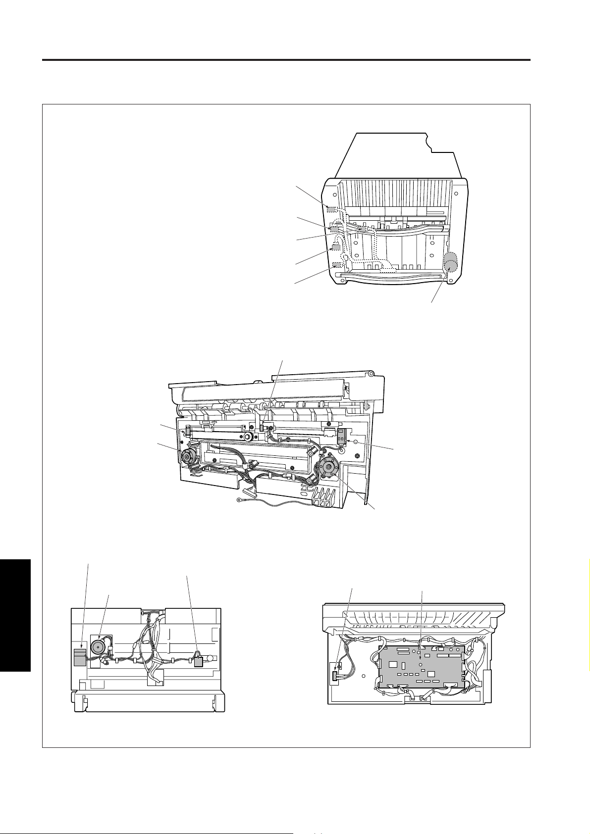
MAIN BODY ELECTRICAL PARTS LAYOUT DRAWING
1
MAIN BODY ELECTRICAL PARTS LAYOUT DRAWING
[1] Switches and sensors
1
TLD Toner level detector
PS9 Tray detect PS (upper)
PS12 Tray detect PS (lower)
PS13 By-pass no paper detect PS
PS20 By-pass tray paper size detect PS
VR1 By-pass tray paper size VR
REVISED EDITION
1
DATE
May 2000
TDS Toner density sensor
PAGE
5-1
5-1
5 DIAGRAMS
METHOD
REPLACEMENT
Page 3
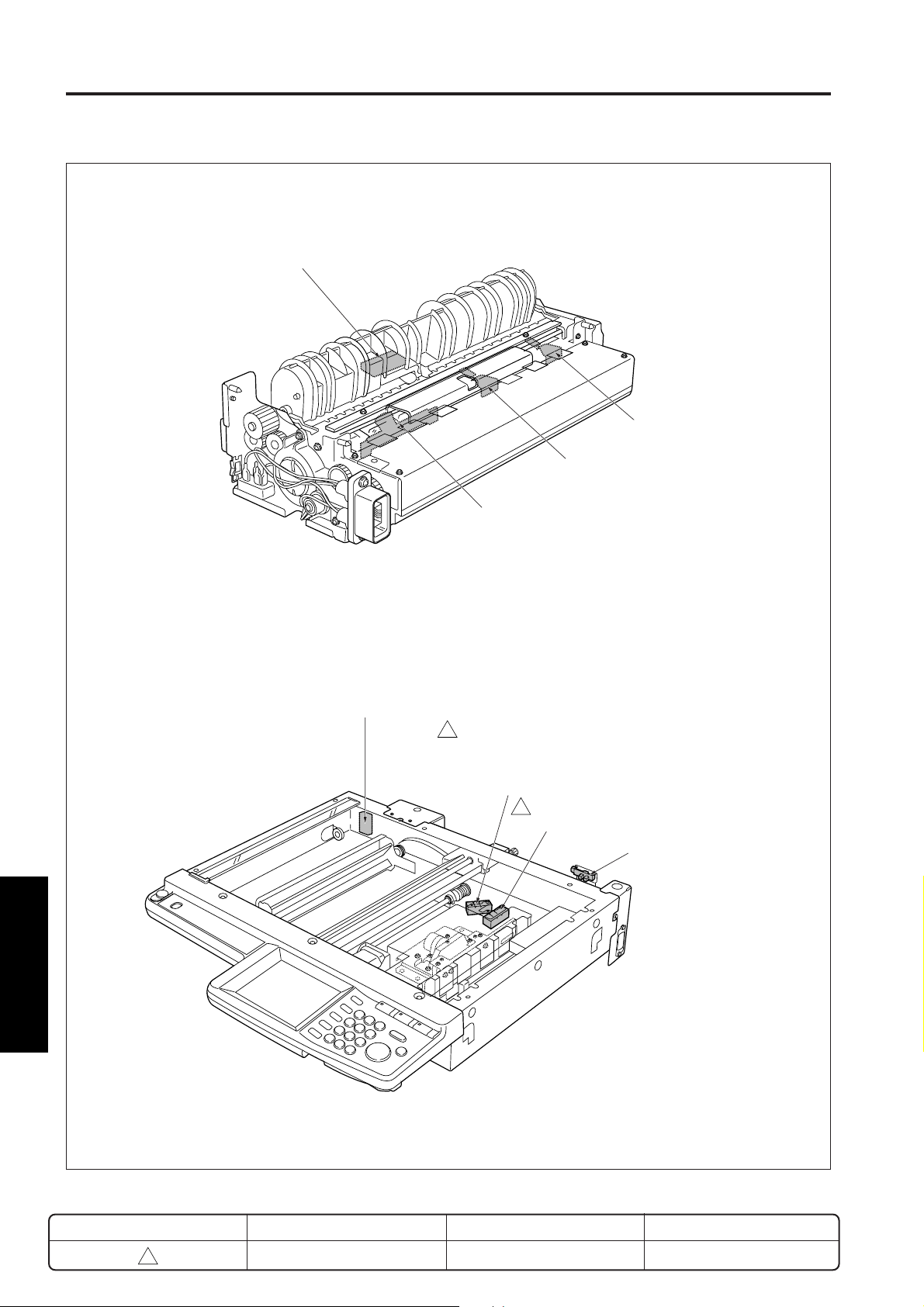
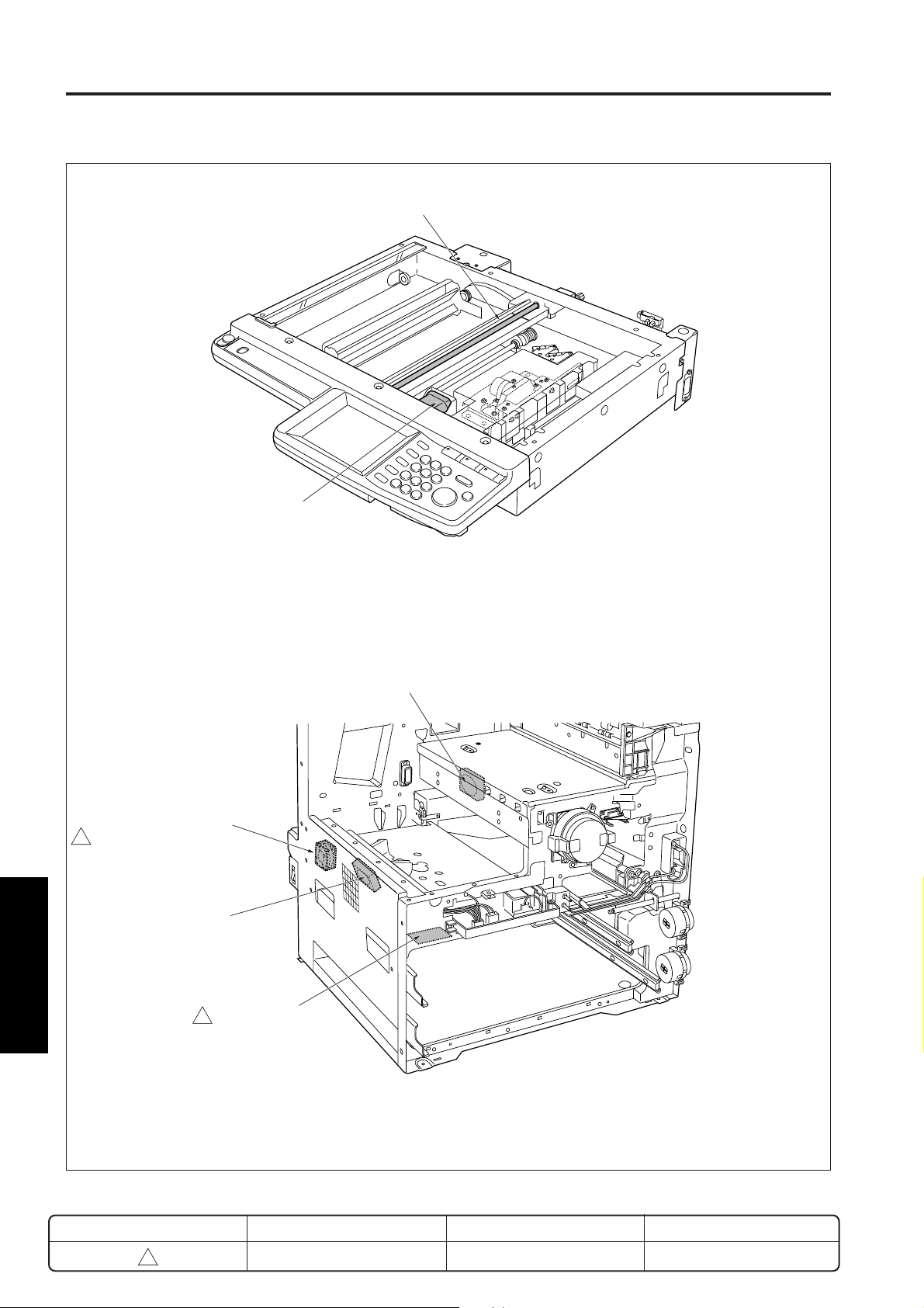
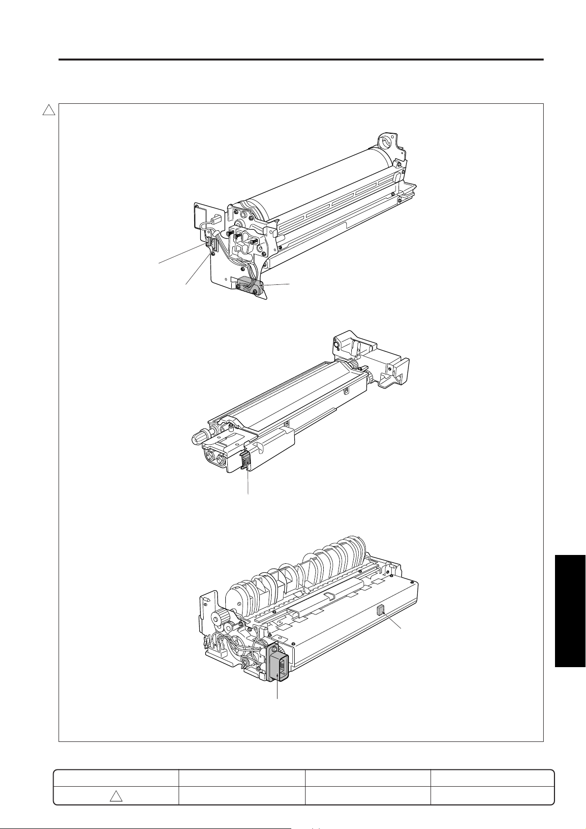
MAIN BODY ELECTRICAL PARTS LAYOUT DRAWING
PS2 Fixing exit PS
TH2 Fixing temperature sensor 2
TH1 Fixing temperature sensor 1
TS Thermostat
5 DIAGRAMS
PS14 Optics home position PS
3
PS17 APS sensor 1
*
Exclusivery for the 7020/25/30/35
PS18 APS sensor 2
*
Exclusivery for machines other than 7020/25/30/35
PS18 APS sensor 2
3
*
Exclusivery for the 7020/25/30/35
PS15 APS timing PS
REVISED EDITION
3
DATE
Jan. 2002
5-2
PAGE
5-2
METHOD
REPLACEMENT
Page 4
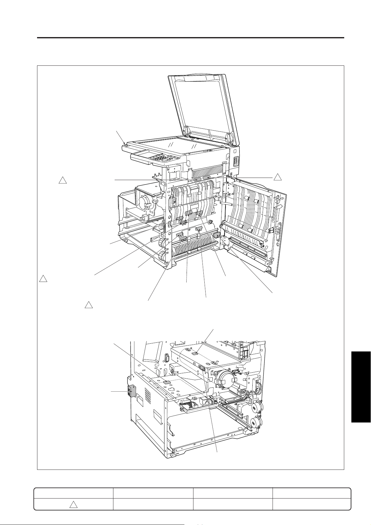
SW2 Sub power switch
PS3 Paper exit PS
3
*
Exclusivery for the
7020/25/30/35
MAIN BODY ELECTRICAL PARTS LAYOUT DRAWING
PS19 Exit limit detect PS
3
* Installed only on old type
7020/25/30/35
PS7 Upper limit
detect PS (upper)
PS21 Intermediate conveyance
3
PS (upper)
* Exclusively for the 7030/7130/7035
PS22 Intermediate conveyance PS
3
HUM1 Humidity sensor
SW1 Main power switch
PS10 Upper
limit detect PS
(lower)
(lower)
* Exclusively for the 7030
PS1 Registration PS
PS8 No paper
detect PS (upper)
PS4 ADU PS
PS11 No paper detect PS (lower)
/7130/7035
PS5 Toner bottle PS
5 DIAGRAMS
REVISED EDITION
3
DATE
Jan. 2002
5-3
SW3 Interlock switch
PAGE
5-3
METHOD
REPLACEMENT
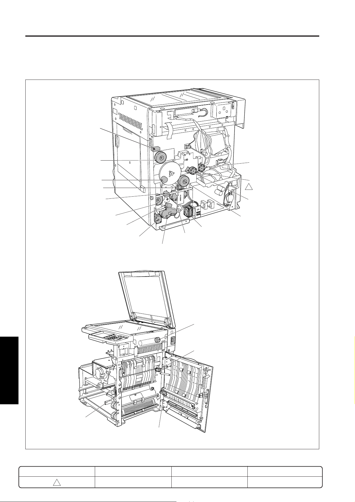
Page 5
MAIN BODY ELECTRICAL PARTS LAYOUT DRAWING
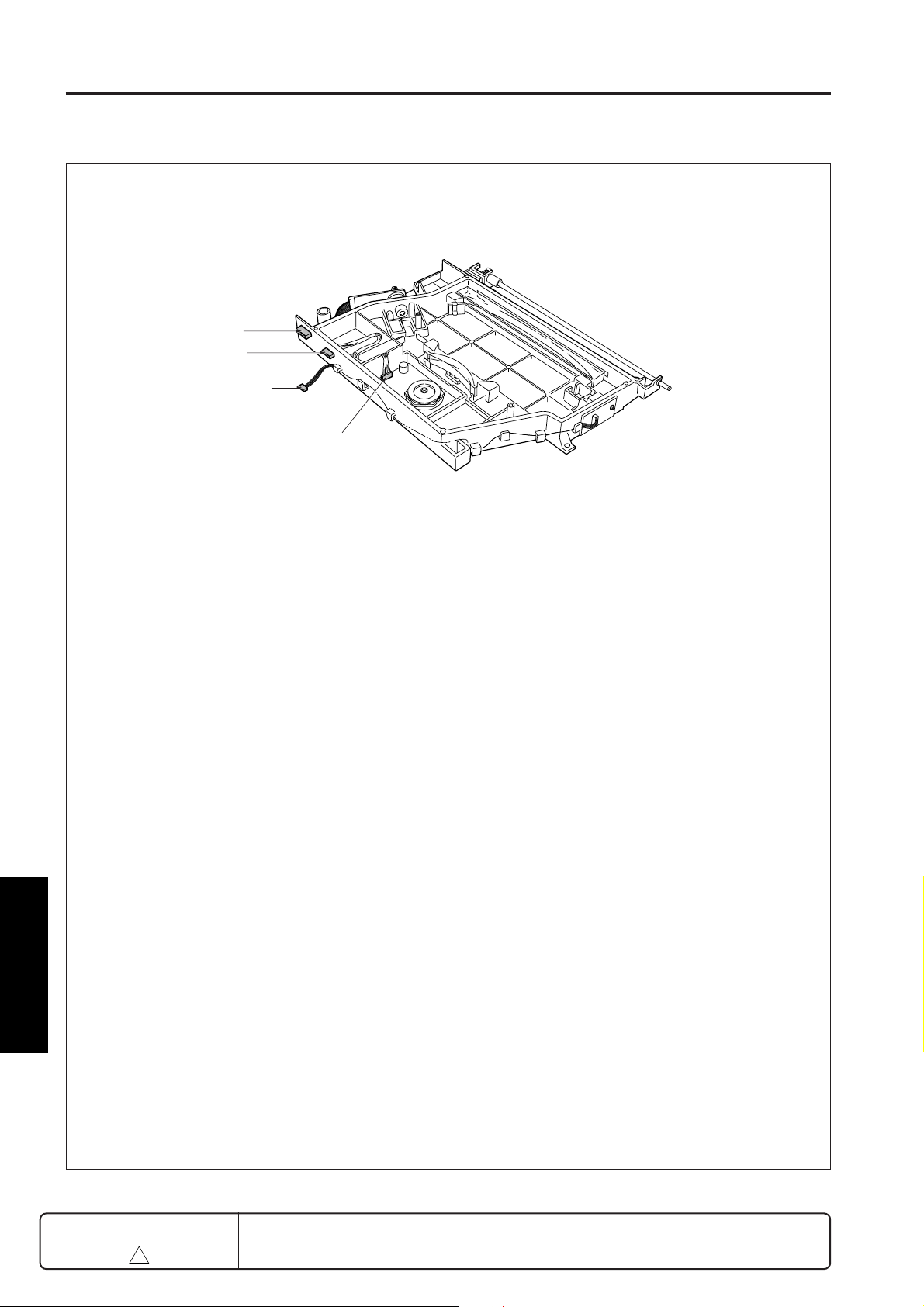
[2] Loads
SD5 ADU gate SD
M1 Main motor
MC1 Registration clutch
SD1 1st paper feed SD (upper)
MC2 Loop clutch
M9 Paper feed motor
SD2 1st paper feed SD (lower)
M6 ADU motor
M7 Tray motor (upper)
M8 Tray motor (lower)
M4 Toner supply motor 1
M10 Toner supply motor 2
*
Exclusivery for machines
3
other than 7020/25/30
SD6 Toner bottle SD
*
Exclusively for the 7020/25/30
M3 Developing motor
FM1 DCPS cooling fan
FM3 Internal dehumidifying fan
5 DIAGRAMS
TSL Transfer synchronisation lamp
REVISED EDITION
3
SD3 By-pass paper feed SD
DATE
5-4
Jan. 2002
SD4 Cleaning web SD
PAGE
5-4
METHOD
REPLACEMENT
Page 6
M5 Polygon motor
MAIN BODY ELECTRICAL PARTS LAYOUT DRAWING
SD7 Separation claw SD
PCL Pre-charging lamp
REVISED EDITION
1
DATE
May 2000
5-5
L2 Fixing heater lamp1
L3 Fixing heater lamp2
PAGE
5-5
5 DIAGRAMS
METHOD
REPLACEMENT
Page 7
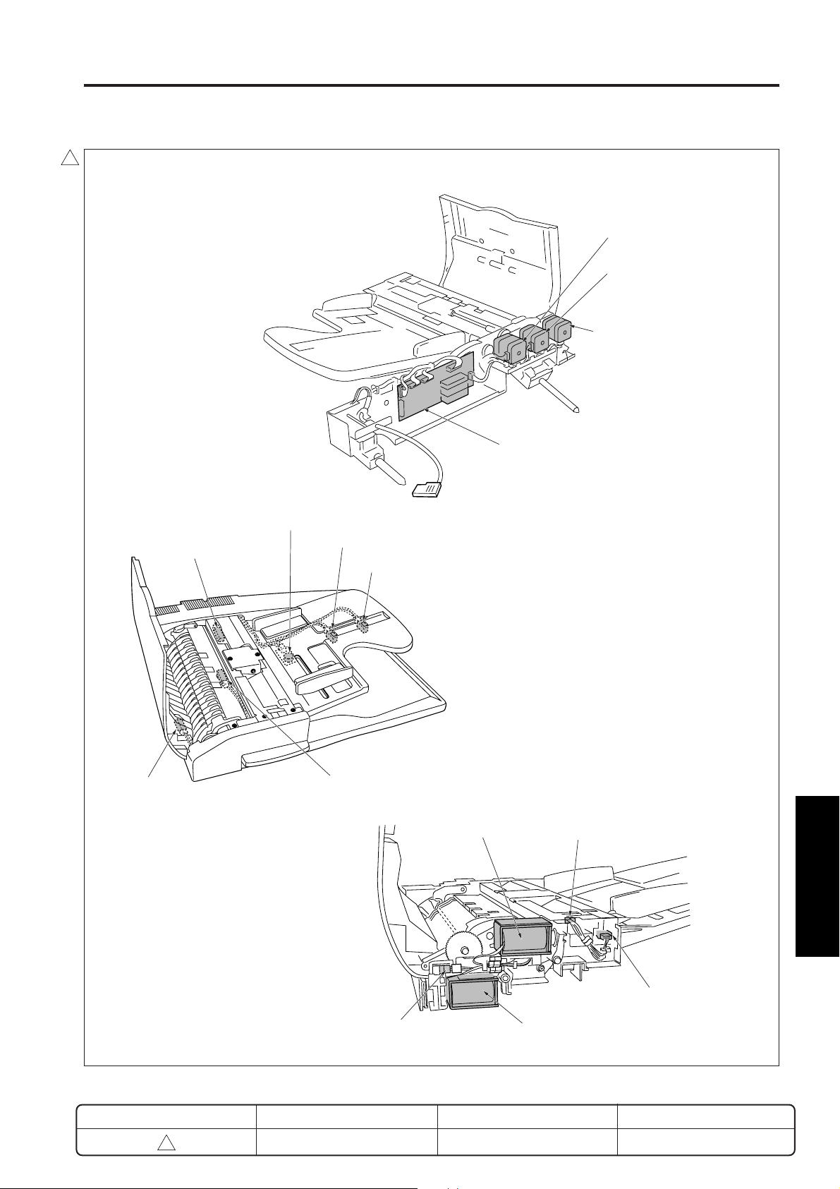
MAIN BODY ELECTRICAL PARTS LAYOUT DRAWING
L1 Exposure lamp
M2 Optical drive motor
FM5 Developing suction fan
*
Exclusively for machines
3
other than 7020/25/30
FM4 Internal cooling fan
5 DIAGRAMS
PTC PTC heater
3
*
Treated as spare parts
in the case of a
machine other than the
7020/25/30/35.
FM2 Fixing cooling fan
REVISED EDITION
3
DATE
Jan. 2002
5-6
PAGE
5-6
METHOD
REPLACEMENT
Page 8

[3] PCBs and others
1
MAIN BODY ELECTRICAL PARTS LAYOUT DRAWING
HV High voltage unit
PRMB Parameter memory board
PFDB (UPPER)
Paper feed detection
board (upper)
PFDB (LOWER)
Paper feed detection
board (lower)
INV1 Exposure lamp inverter
PRDB Printer drive board
CBR2 Circuit breaker 2
CBR1 Circuit breaker 1
CB Overall control board
PSWB Power SW board
PAKB Panel key board
REVISED EDITION
1
DCPS DC power supply unit
LCD display board
INV2 display inverter
DATE
May 2000
OB operation board
5-7
PAGE
5-7
L1INVB Exposure lamp
power supply board
5 DIAGRAMS
ADB A/D conversion
board
SCDB scanner drive board
METHOD
REPLACEMENT
Page 9
MAIN BODY ELECTRICAL PARTS LAYOUT DRAWING
1
LDB LD drive board
INDEX Index sensor board
TCSB Toner control sensor board
5 DIAGRAMS
REVISED EDITION
1
DATE
May 2000
5-8
PAGE
5-8
METHOD
REPLACEMENT
Page 10
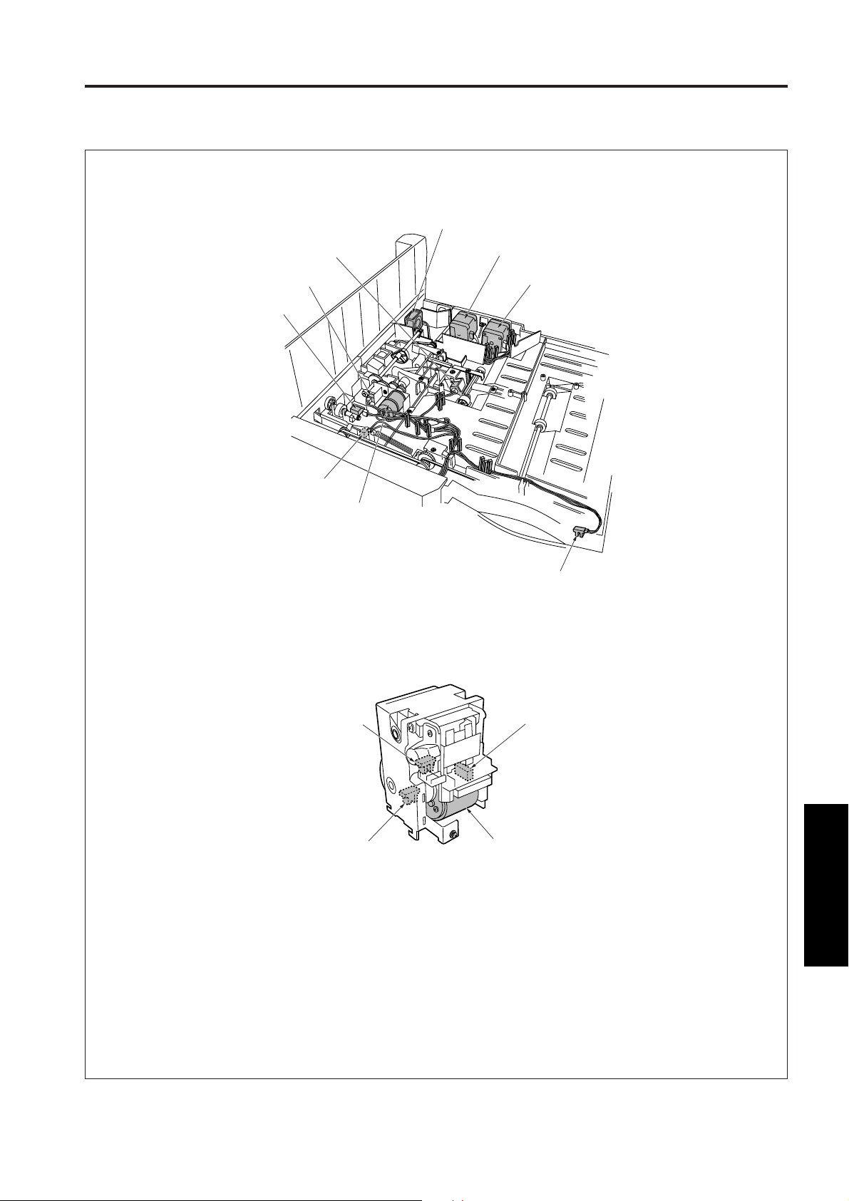
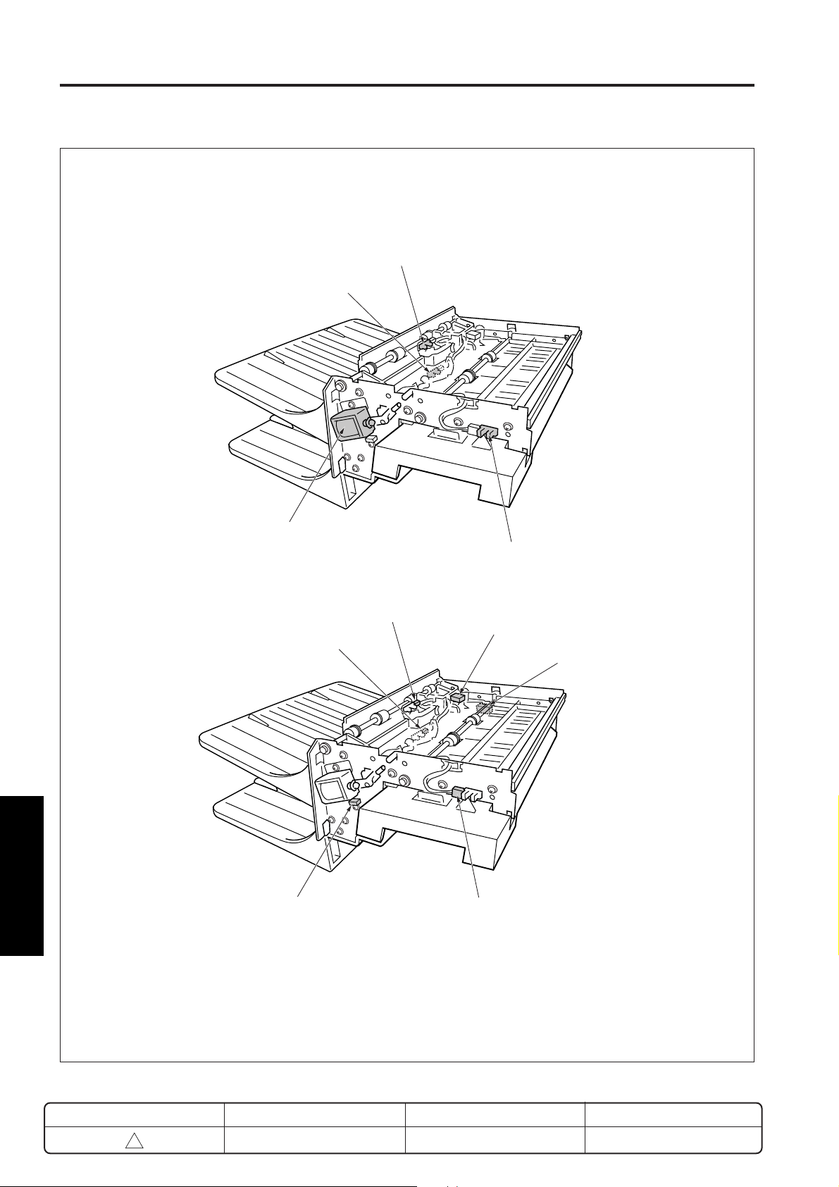
DF-314 ELECTRICAL PARTS LAYOUT DRAWING
DF-314 ELECTRICAL PARTS LAYOUT DRAWING
1
M301 Original feed motor
M303 Original reversal motor
M302 Original conveyance motor
DFCB RADF control board
PS303 Original exit PS
PS312 Original feed PS
VR301 Size detect VR
PS306 Original detect PS1
PS311 Original registration PS
PS307 Original detect PS2
SD302 Rollar pressure SD
PS305 Cover open/close detect PS
5 DIAGRAMS
REVISED EDITION
1
PS304 RADF open/close detect PS
DATE
5-9
May 2000
SD303 Exit SD
PAGE
5-9
PS301 No original detect PS
METHOD
REPLACEMENT
Page 11
FS-107 ELECTRICAL PARTS LAYOUT DRAWING
FS-107 ELECTRICAL PARTS LAYOUT DRAWING
PS711 Tray upper limit detect PS
PS704 Tray full-stack detect PS
PS703 Paper exit detect PS
PS716 Tray count PS
PS706 Tray lower limit detect PS
M706 Tray up/down motor
PS709 Alignment plate
detect PS (rear)
M703 Alignment motor (rear)
M706 Tray up/down motor
M705 Stapler shift motor
PS707 No paper detect PS
PS708 Stapler unit HP detect PS
M704 Alignment motor (front)
MS701 Front door switch
PS710 Alignment plate
detect PS (front)
FSCB FS control board
5 DIAGRAMS
5-10
Page 12
FS-107 ELECTRICAL PARTS LAYOUT DRAWING
M709 Cooling fan motor
PS702 Paper entrance detect PS
PS701 Paper pressure PS
PS705 Shutter PS
MS702 Shutter switch
M707 Paper pressure motor
M702 Paper exit motor
M701 Paper conveyance motor
PS717 Conveyance cover open/close detect PS
PS714 Stapler ready detect PS
PS712 Stapler HP detect PS
M708 Stapler motorPS713 No-staple PS
5 DIAGRAMS
5-11
Page 13
DB-209/210 ELECTRICAL PARTS LAYOUT DRAWING
DB-209/210 ELECTRICAL PARTS LAYOUT DRAWING
PS104 Jam detect PS1
PS102 Upper limit detect PS (upper)
PS103 No paper detect PS (upper)
PTC heater
3
*
Treated as a spare parts in
the case of new type DB
SDB1 Size detection board 1
SDB1 Size detection board 2
PS107 Upper limit detect PS (lower)
SD101 1st paper feed SD (upper)
M100 Paper feed motor
PS108 No paper detect PS (lower)
PS105 Jam detect PS2
PS101 Tray detect PS (upper)
PS106 Tray detect PS (lower)
5 DIAGRAMS
REVISED EDITION
3
M101 Tray motor1
M102 Tray motor2
SD102 1st paper feed SD (lower)
DATE
5-12
Jan. 2002
PAGE
5-12
PFUDB PFU drive board
METHOD
REPLACEMENT
Page 14
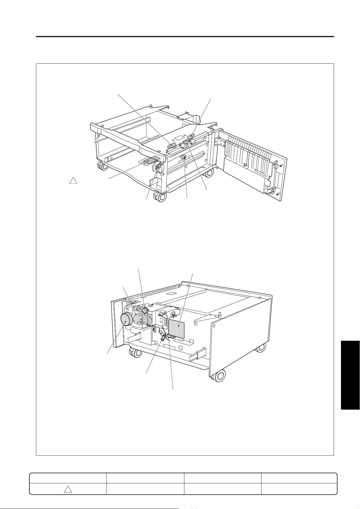
DB-409/410 ELECTRICAL PARTS LAYOUT DRAWING
DB-409/410 ELECTRICAL PARTS LAYOUT DRAWING
PS102 Paper level detect PS1
PTC Heater
3
*
Treated as a spare parts in
the case of new type DB
SDB 1 Size detection board 1
SD101 1st paper feed SD
PS103 No paper detect PS
PS104 Jam detect PS1
PS105 Jam detect PS2
LCTDB LCT drive board
M101 Tray motor
M100 Paper feed motor
PS101 Tray detect PS
PS109 Paper level detect PS2
5 DIAGRAMS
REVISED EDITION
3
DATE
Jan. 2002
5-13
PAGE
5-13
METHOD
REPLACEMENT
Page 15
IT-101 ELECTRICAL PARTS/CONNECTOR LAYOUT DRWING
IT-101 ELECTRICAL PARTS/CONNECTOR LAYOUT DRAWING
PS23 IT exit PS (upper)
PS24 IT exit PS (lower)
5 DIAGRAMS
SD8 IT gate SD
PS25 IT door PS
CN972 (W:3pin)
J43 (W:8pin)
CN973 (W:3pin)
J42 (BK:12pin)
CN292 (W:2pin) CN974 (W:3pin)
REVISED EDITION
2
DATE
Feb. 2001
5-14
PAGE
5-14
METHOD
ADDITION
Page 16
MAIN BODY CONNECTOR LAYOUT DRAWING
MAIN BODY CONNECTOR LAYOUT DRAWING
J42 (BK:12pin)
3
J915 (W:6pin)
* Exclusively for machines
other than 7020/25/30
3
CN927 (W:2pin)
*
Exclusively for the 7020/25/30
J05 (W:3pin)
CN921 (B:2pin)
J30 (W:3pin)
J04 (W:11pin)
CN905 (W:6pin)
J03 (W:11pin)
J12 (W:9pin)
J28 (B:3pin)
J21 (W:3pin)
J23 (W:4pin)
CN903 (W:8pin)
J06 (W:3pin)
J 903 (W:6pin)
CN9 (W:3pin)
J14 (W:6pin)
J31 (W:3pin)
CN922 (W:2pin)
J32 (W:3pin)
CN923 (W:2pin)
J02 (W:7pin)
REVISED EDITION
3
DATE
Jan. 2002
5-15
CN930 (W:2pin)
PAGE
5-15
5 DIAGRAMS
METHOD
REPLACEMENT
Page 17
MAIN BODY CONNECTOR LAYOUT DRAWING
J50 (W:12pin)
J51 (W:5pin)
J52 (W:5pin)
CN904 (5pin)
5 DIAGRAMS
REVISED EDITION
1
DATE
May 2000
5-16
PAGE
5-16
METHOD
REPLACEMENT
Page 18
MAIN BODY CONNECTOR LAYOUT DRAWING
1
J928 (W:2pin)
J11 (W:7pin)
J16 (BK:18pin)
J17 (BK:10pin)
REVISED EDITION
1
DATE
May 2000
J13 (BK:8pin)
5-17
PAGE
5-17
J13 (W:4pin)
5 DIAGRAMS
METHOD
REPLACEMENT
Page 19

MAIN BODY CONNECTOR LAYOUT DRAWING
Overall control board
CN39
(25pin)
CN40
(36pin)
CN32
(20pin)
CN46
(50pin)
CN800
(68pin)
CN37
(120pin)
CN33
(24pin)
CN48
(20pin)
CN801
(68pin)
CN47
(22pin)
CN34
(24pin)
CN803
(6pin)
CN500
CN30
(6pin)
CN431
(5pin)
(4pin)
CN432
(12pin)
CN45
(11pin)
CN44
(19pin)
CN42
(9pin)
CN38
(100pin)
3
CN31
(8pin)
High voltage unit Printer drive board
CN70
(9pin)
CN72
(3pin)
5 DIAGRAMS
CN71
(12pin)
CN28
(
38 pin
(
CN37
(
)
8 pin
CN38
(
)
4 pin
CN35
(
)
5 pin
CN36
(
)
10 pin
CN601
3
(
10 pin
*
Exclusively for the machines
other than 7020/25/30
CN19
(
24 pin
)
)
CN29
36 pin
CN25
(
34 pin
)
CN23
(
22 pin
)
)
CN26
(
26 pin
3
CN79
(6
)
pin
)
*
Exclusively for the
CN27
(
)
8 pin
CN24
(
)
40
pin
)
7030/7130/7035
CN20
(
)
4 pin
CN21
(
)
6 pin
CN22
(
)
5 pin
REVISED EDITION
3
DATE
Jan. 2002
5-18
PAGE
5-18
METHOD
REPLACEMENT
Page 20

MAIN BODY CONNECTOR LAYOUT DRAWING
DC power supply unit A/D conversion board
CN1
(5pin)
CN2
(14pin)
CN3
(5pin)
CN7
(26pin)
CN8
(4pin)
CN5
(4pin)
CN6
(20pin)
CN10
(3pin)
CN60
(50pin)
Scanner drive board Operation board
<Other than 7035>
3
CN62
(
3 pin
CN66
(
7 pin
CN65
(
8 pin
<7035>
CN62
(
3 pin
CN66
(
7 pin
CN65
(
8 pin
)
)
)
CN60
(
10 pin
)
)
)
CN60
(
10 pin
)
CN63
(
4 pin
)
CN63
(
4 pin
CN64
(
15 pin
)
CN64
(
7 pin
)
CN68
(
)
8 pin
Exclusively for the
*
CN61
(
)
11 pin
)
CN61
(
)
11 pin
CN67
(
)
6 pin
)
3
<Other than 7020/25/30/35>
CN81
(13pin)
<7020/25/30/35>
CN81
(13pin)
CN87
(2pin)
CN86
(14pin)
CN86
(14pin)
(12pin)
(12pin)
CN80
CN80
CN82
(5pin)
CN82
(5pin)
CN84
(18pin)
CN84
(18pin)
CN83
(4pin)
5 DIAGRAMS
CN83
(4pin)
REVISED EDITION
3
DATE
Jan. 2002
5-19
PAGE
5-19
METHOD
REPLACEMENT
Page 21

MAIN BODY CONNECTOR LAYOUT DRAWING
LD drive board Index senser board
CN50
(12pin)
Toner control sensor board Power SW board
CN1
(7pin)
CN51
(5pin)
CN1
(3pin)
Paper feed detection board (upper, lower) Parameter memory board
5 DIAGRAMS
REVISED EDITION
1
CN1
(5pin)
DATE
May 2000
5-20
PAGE
5-20
CN2
(24pin)
CN1
(20pin)
METHOD
REPLACEMENT
Page 22

Exposure lamp power supply board
MAIN BODY CONNECTOR LAYOUT DRAWING
CN97 (2pin)
Display inverter
CN77
(4pin)
CN96 (2pin)
CN71
(3pin)
Exposure lamp inverter
CN931
(4pin)
REVISED EDITION
1
CN930
(3pin)
DATE
May 2000
5-21
PAGE
5-21
5 DIAGRAMS
METHOD
REPLACEMENT
Page 23

DF-314 CONNECTOR LAYOUT DRAWING
DF-314 CONNECTOR LAYOUT DRAWING
1
CN130 (W:6pin)
CN132 (W:6pin)
CN131 (W:6pin)
CN200 (GY:18pin)
CN123 (W:3pin)
CN113 (W:3pin)
CN117 (W:3pin)
CN116 (W:3pin)
CN1 (18pin)
CN3 (7pin)
CN6 (15pin)
CN5 (8pin)
CN4 (9pin)
DFCB
CN7 (30pin)
CN2 (22pin)
CN122 (W:3pin)
5 DIAGRAMS
REVISED EDITION
1
CN121 (W:3pin)
May 2000
DATE
CN114 (W:3pin)
5-22
CN136 (BK:2pin)
CN137 (W:2pin)
PAGE
5-22
CN115 (W:3pin)
CN111 (W:3pin)
CN105 (W:3pin)
METHOD
REPLACEMENT
Page 24

FS-107 CONNECTOR LAYOUT DRAWING
FS-107 CONNECTOR LAYOUT DRAWING
CN736 (B:3pin)
CN735 (W:3pin)
CN734 (W:3pin)
CN744 (W:3pin)
CN737 (B:3pin)
CN756 (W:15pin)
CN741 (W:3pin)
CN724 (W:6pin)
CN756 (W:15pin)
CN738 (W:3pin)
CN723 (B:6pin)
CN725 (W:6pin)
CN740 (B:3pin)
CN756 (W:15pin)
CN739 (W:3pin)
CN726 (BK:2pin)
5 DIAGRAMS
CN751 (W:1pin)
5-23
Page 25

FS-107 CONNECTOR LAYOUT DRAWING
CN753 (W:2pin) CN752 (W:3pin)
CN709 (12pin)
CN715 (30pin)
CN706 (2pin)
CN714 (15pin)
CN701 (10pin)
CN712 (2pin)
FS CB
CN711 (2pin)
CN704 (12pin)
CN702 (11pin)
CN713 (3pin)
CN710 (2pin)
CN733 (W:3pin)
CN732 (W:3pin)
CN300 (BK:24pin)
CN708 (8pin)
CN731 (W:3pin)
CN703 (12pin)
CN705 (W:6pin)
CN722 (W:6pin)
CN721 (W:6pin)
CN707 (30pin)
5 DIAGRAMS
CN734 (W:3pin)
CN730 (BK:2pin)
CN745 (W:3pin)
5-24
Page 26

DB-209/210 CONNECTOR LAYOUT DRAWING
2
DB-209/210 CONNECTOR LAYOUT DRAWING
CN102
2
(DB-209:6pin)
(DB-210:11pin)
PFU drive board
CN100
(6pin)
CN103
(24pin)
CN101
(26pin)
CN104
(19pin)
J70 (W:6pin)
J69 (W:6pin)
CN1
(5pin)
Size detection board 2Size detection board 1
CN1
(5pin)
J68 (W:7pin)
CN113 (W:12pin)
J64 (W:8pin)
J66 (W:3pin)
5 DIAGRAMS
J67 (W:3pin)
J63 (W:6pin)
J65 (W:11pin)
REVISED EDITION
2
DATE
Feb. 2001
5-25
PAGE
5-25
METHOD
REPLACEMENT
Page 27

DB-409/410 CONNECTOR LAYOUT DRAWING
2
DB-409/410 CONNECTOR LAYOUT DRAWING
CN102
2
(DB-409:6pin)
(DB-410:11pin)
LCT drive board
CN100
(6pin)
CN103
(24pin)
CN101
(26pin)
CN105
(DB-410:3pin)
Size detection board 1
CN1
(5pin)
CN105
(DB-409:3pin)
J69 (W:6pin)
CN113 (W:2pin)
5 DIAGRAMS
J68 (W:3pin)
J64 (W:8pin)
J66 (W:3pin)
J63 (W:6pin)
REVISED EDITION
2
DATE
Feb. 2001
5-26
PAGE
5-26
METHOD
REPLACEMENT
Page 28

LIST OF JAM CODES
During operation
LIST OF JAM CODES
Classification
By-pass
Upper tray
Lower tray
DB tray
Conveyance
Fixing/exit
ADU
conveyance
FS-107
3
7020/25/30/
35 only
3
7020/25/30/
35 only
J72-16
J72-17
J72-19
Code
J10
J11
J12
J13
J14
J16
J30
J31
J32
J32-2
J33
J92
J97-1
J97-2
Causes
PS1 (registration) failed to turn ON within a
predetermined time after start of by-pass feed
(after SD3 (by-pass) ON).
PS1 (registration) failed to turn ON within a
predetermined time after start of upper-tray
feed (after SD1 (first paper-feed (upper)) ON).
PS1 (registration) failed to turn ON within a
predetermined time after start of upper-tray
feed (after SD2 (first paper-feed (lower)) ON).
PS104 (jam detect 1) failed to turn ON within a
predetermined time after start of feed from DB
upper tray (after SD101 (first paper-feed
(upper)) ON).
PS104 (jam detect 1) failed to turn ON within a
predetermined time after start of feed from DB
lower tray.
PS1 (registration) failed to turn ON within a
predetermined time after paper passed PS104
(jam detect 1).
• DB upper tray feed
• DB lower tray feed
PS1 (registration) failed to turn OFF within a
predetermined time after MC1 (registration) ON.
PS2 (fixing exit) failed to turn OFF within a
predetermined time after MC1 (registration) ON.
PS3 (paper exit) failed to turn ON within a
predetermined time after PS2 (fixing exit) ON.
(At the single side copy mode)
PS2 (fixing exit) failed to turn OFF within a
predetermined time after turning ON.
PS3 (paper exit) failed to turn OFF within a
predetermined time after turning ON.
PS1 (registration) failed to turn ON within a
predetermined time after start of ADU reversal.
PS4 (ADU) failed to turn ON within a
predetermined time after PS2 (fixing exit) ON.
PS4 (ADU) failed to turn OFF within a
predetermined time after turning ON.
PS702 (paper entrance detect) failed to turn ON within
a predetermined time after PS3 (paper exit) ON.
PS702 (paper entrance detect) failed to turn ON within a
predetermined time after PS707 (no paper detect) ON.
(Straight, sort/group mode for other than small size)
PS702 (paper entrance detect) failed to turn OFF
within a predetermined time after turning ON.
(Staple, sort/group, and small size straight modes)
Resulting
If copying is in
progress at time
of jam, the
copier
completes
ejection and
then stops.
The main body
stops
immediately.
The FS-107 and
main body stop
immediately.
operation
Correction
Take out the paper from the
bypass tray, and remove
any jammed paper.
Open the ADU door,
remove any jammed paper,
and close the door.
Pull out the tray, and
remove any jammed paper.
Open the DB conveyance
door, remove any jammed
paper, and close the door.
Pull out the tray, and
remove any jammed paper.
Open the ADU door and/or
DB conveyance door,
remove any jammed paper,
and close the door.
Open the ADU door,
remove any jammed paper,
and close the door.
Open the finisher front door,
and conveyance cover
remove any jammed paper,
and close the door.
5 DIAGRAMS
REVISED EDITION
3
DATE
Jan. 2002
5-27
PAGE
5-27
METHOD
REPLACEMENT
Page 29

LIST OF JAM CODES
Classification
FS-107
IT-101
DF-314
5 DIAGRAMS
Code
J72-21
J72-23
J72-81
J75-10
J75-11
3
J75-12
J75-13
PS707 (No paper detect) failed to turn OFF within a
predetermined time after M702 (Paper exit) turning ON.
(Staple, sort/group, and small size straight modes)
PS707 (No paper detect) failed to turn OFF within
a predetermined time after turning ON. (Straight,
sort/group mode for other than small size)
Staple jam: M708 (stapler) failed to turn OFF
within a predetermined time after turning ON.
(Forward operation not completed.) (Staple mode)
PS23 (IT paper exit (upper)) does not go ON within a
predetermined time after PS3 (paper exit) (in the case of a
machine other than 7020/25/30/35, PS2 (fixing exit)) goes ON.
PS24 (IT exit (lower)) is not turned ON within a
predetermined time after PS3 (paper exit) (in the case
of the 7020/25/30/35, PS2 (fixing exit)) is turned ON.
PS3 (paper exit) (in the case of machines other
than the 7020/25/30/35, PS2 (fixing exit)) does
not go OFF within a predetermined time after
PS23 (IT paper exit (upper)) or PS24 (IT paper
exit (lower)) goes ON.
The IT door of the IT-101 opened while the main
body was operating.
J61-0
PS305 (cover open/close detect) turned ON.
(The paper feed cover is opened.)
J61-1
PS304 (RADF open/close detect) turned ON.
J62-0
Original did not feed.
J62-2
PS312 (original feed) failed to turn ON within a
predetermined time after start of refeed for
single sided original.
J62-3
PS312 (original feed) failed to turn ON within a
predetermined time after start of reverse exit for
double sided original.
J62-4
PS312 (original feed) did not go OFF within the
specified period after it went ON, during paper exit.
J62-5
PS312 (original feed) did not go OFF within the
specified period after it went ON, during reversal.
J63-0
PS303 (original exit) did not go ON during
paper exit.
J63-2
PS303 (original exit) did not go OFF within the
specified period after it went ON, during paper
exit.
J63-4
PS311 (original registration) failed to turn OFF
within a predetermined time after start of refeed
of single sided original.
J63-5
PS311 (original registration) failed to turn OFF within
a predetermined time after start of reverse feed.
Causes
Resulting
operation
The FS-107
and main body
stop
immediately.
The main body
stops
immediately.
The DF-314
stops
immediately.
Correction
Open the finisher front
door, and conveyance
cover remove any jammed
paper, and close the door.
Remove the jammed
staple.
Open the IT door, and
remove the jammed paper,
then close the door.
Open the RADF, remove
any jammed paper, and
then close.
Remove any jammed
paper from the main body's
conveyance section.
REVISED EDITION
3
DATE
Jan. 2002
5-28
PAGE
5-28
METHOD
REPLACEMENT
Page 30

LIST OF JAM CODES
Others
J20-2
J20-3
J20-4
J20-5
J20-6
J50-1
J50-2
J50-3
ADU door open jam
SW3 (Interlock switch) went OFF during printing.
FNS front door open jam
MS701 (front door) went OFF during printing.
System emergency stop jam
FNS conveyance door open jam
PS717 (conveyance cover open/close detect)
went OFF during printing.
FNS shutter switch operation jam
MS702 (shutter) went ON during printing.
Failed to receive print request from system within
a predetermined time after PS1 (registration) ON.
“Valid” signal failed to turn ON within a
predetermined time after start of printing.
MC1 (registration) failed to turn ON within a
predetermined time after start of printing.
Printer section
stops
immediately.
Machine stops
immediately.
Remove jammed paper
according to message.
Opne the ADU door,
remove any jammed paper,
and close the door.
Classification
Code
Causes
Resulting
operation
Correction
3
REVISED EDITION
3
DATE
Jan. 2002
5-29
PAGE
5-28-1
5 DIAGRAMS
METHOD
REPLACEMENT
Page 31

When idling
LIST OF JAM CODES
Classification
Paper feed
Exit
ADU
FS-107
DF-314
IT-101
3
Code
J81
J82
J90
J91
J100
J72-1
J72-2
J65-1
J65-2
J65-3
J65-8
J65-9
J65-10
J65-11
J75-10
Causes Correction
PS1 (registration) ON during idling state.
PS105 (Jam detect 2) ON during idling state.
PS2 (fixing exit) ON during idling state.
PS3 (paper exit) ON during idling state.
(7020/25/30/35 only)
PS4 (ADU) ON during idling state.
PS702 (paper entrance detect) ON during
idling state.
PS707 (no paper detect) ON during idling
state.
PS311 (original registration) ON during idling
state.
PS312 (original feed) ON during idling state.
PS311 (original registration), PS312 (original
feed) ON during idling state.
PS303 (original exit) ON during idling state.
PS311 (original registration), PS303 (original
exit) ON during idling state.
PS312 (original feed), PS303 (original exit) ON
during idling state.
PS311 (original registration), PS312 (original
feed), PS303 (original exit) ON during idling
state.
PS23 (IT exit (upper)) or PS24 (IT exit (lower))
went ON during idling.
Open the ADU door, remove jammed paper,
and close the door.
Open the DB feed door, remove jammed
paper, and close the door.
If paper is jammed in the main body: open
the ADU door, remove the jammed paper,
and close the door.
Open the ADU door, remove jammed paper,
and close the door.
Open the ADU door, remove jammed paper,
and close the door.
Open the finisher door, remove jammed
paper, and close the door.
Open the RADF, remove jammed paper,
and then close.
Open the IT door, remove jammed paper,
then close the door.
REVISED EDITION
3
DATE
Jan. 2002
5-31
PAGE
5-29
METHOD
REPLACEMENT
Page 32

LIST OF WARNING (ERROR) CODES
LIST OF WARNING (ERROR) CODES
Classification
Communication
abnormalities
Feed-tray and
drum-area
abnormalities
5 DIAGRAMS
Warning
code
F10-1
F10-2
F10-9
F18-1
F18-2
F18-3
F18-4
F22-1
F23-1
Causes
Failure in serial
communication between the
PRDB (printer drive board)
and CB (overall control board).
Two consecutive failures to
respond to PRDB (printer drive
board) A/D conversion request.
Communication error at PRDB
(printer drive board)
SRGA (serial gate array) error.
(Error in protocol for receive
control signals SREC, SACK.)
Error in main body upper tray
PS7 (tray upper limit detect
(upper)) failed to turn ON
within 26 seconds after M7
(tray (upper)) ON.
Error in main body lower tray
PS10 (tray upper limit detect
(lower)) failed to turn ON
within 26 seconds after M8
(tray (lower)) ON.
Error in DB upper tray
PS102 (upper limit detect
(upper)) failed to turn ON
within 26 seconds after M101
(tray 1) ON.
Error in DB lower tray
PS107 (upper limit detect
(lower)) failed to turn ON
within 26 seconds after M102
(tray 2) ON.
Internal overheating
The temperature at the
outside of the drum reached or
exceeded 47˚C.
PCL connector detached
With 24V ON and PCL OFF,
the PCL EM signal (pcl_em)
was detected as "H" (software
logic).
Resulting
operation
If copying is in
progress, the
main body
stops
immediately,
and the main
relay and 24V
power turn
OFF.
Correction Estimated abnormal parts
Switch SW2 (sub
power switch)
OFF and then
back ON.
Switch SW2 (sub
power switch) OFF,
connect the PCL
connector, and then
set SW2 ON.
PRDB (printer drive board)
CB (overall control board)
PRDB (printer drive board)
PRDB (printer drive board)
CB (overall control board)
PRDB (printer drive board)
M7 (tray (upper))
PS7 (tray upper limit detect
(upper))
PRDB (printer drive board),
M8 (tray (lower))
PS10 (tray upper limit detect
(lower))
PFU DB (PFU drive board)
or LCT DB (LCT drive board)
M101 (tray 1)
PS102 (upper limit detect
(upper))
PFU DB (PFU drive board)
M102 (tray 2)
PS107 (upper limit detect
(lower))
TCSB (toner-control sensor
1
board)
FM4 (internal cooling)
PCL connector
PRDB (printer drive board)
REVISED EDITION
1
DATE
May 2000
5-30
PAGE
5-30
METHOD
REPLACEMENT
Page 33

LIST OF WARNING (ERROR) CODES
Classification
High voltage
unit abnormalities
3
Fixing high
temperature
abnormalities
Warning
code
F26-1
F26-2
F26-3
F28-1
F28-2
F28-3
F34-1
F34-2
Causes Correction Estimated abnormal parts
L detection data error
If L detection power exceeds 26V
prior to toner out detection by the
TLD (toner level detect), the
automatic toner supply feature
should restore the toner density.
This error occurs if this feature
fails to restore the density.
Abnormal output from TDS
(toner density sensor)
Maximum TDS output voltage
failed to exceed 1.0V.
Abnormal output from TDS
(toner density sensor)
TDS output ripple voltage
failed to reach 0.5V
Charging error
EM detect signal
(charge_em1) was read 3
times at 100msec intervals.
Abnormal transfer spark (trans_em)
detected 3 times at 20msec
intervals, 5 times in succession for
the same job.
Abnormal separation spark
(separate_em) detected 5 times
at 20msec intervals, 5 times in
succession for the same job.
TH1 (fixing temperature sensor
1) detected abnormally high
temperature.
Temperature detected by TH1
remained at or above 231˚C for
0.4 seconds.
TH2 (fixing temperature sensor
2) detected abnormally high
temperature.
Temperature detected by TH2
remained at or above 231˚C for
0.4 seconds.
If copying is in
progress, the
main body
stops
immediately,
and the main
relay and 24V
power turn
OFF.
Main relay and 24
V power supply
go OFF at the
end of the job.
If copying is in
progress, the
main body
stops
immediately,
and the main
relay and 24V
power turn
OFF.
Main relay
turns OFF and
acceptance of
all keys is
disabled.
Resulting
operation
Set SW2 (sub
power switch)
OFF and then
back ON.
Set SW2 (sub
power switch)
OFF and then
back ON after set
to "0" the bit 1 in
DIP SW3 in 25
mode. (If you
switch power back
on without
releasing the
latch, the error will
recur.)
TDS (toner density sensor)
TLD (toner level detect
sensor)
PRDB (printer drive board)
Toner supply unit
TDS (toner density sensor)
PRDB (printer drive board)
Developer
TDS (toner density sensor)
PRDB (printer drive board)
M1 (main)
Developer agitating screw
Developing unit connector
Charging corona unit
HV (high voltage unit)
PRDB (printer drive board)
Transfer corona unit
HV (high voltage unit)
PRDB (printer drive board)
Separation corona unit
HV (high voltage unit)
PRDB (printer drive board)
TH1 (fixing temperature sensor 1)
TH2 (fixing temperature sensor 2)
L2 (fixing heater lamp 1)
L3 (fixing heater lamp 2)
PRDB (printer drive board)
DCPS (DC power supply)
5 DIAGRAMS
REVISED EDITION
3
DATE
Jan. 2002
5-31
PAGE
5-31
METHOD
REPLACEMENT
Page 34

LIST OF WARNING (ERROR) CODES
1
Classification
Fixing low
temperature
abnormalities
Warning
code
F35-1
F35-2
F35-3
F35-4
F35-5
Causes Correction Estimated abnormal parts
T
H1 (fixing temperature sensor 1)
detected abnormally low temperature.
Occurs if main motor remains
energized for longer than 10
seconds during idling state.
T
H1 (fixing temperature sensor 1)
detected abnormally low temperature.
During idling or copying, TH1
detected that temperature remained
at or below 165˚C for 10 seconds.
TH1 (fixing temperature sensor 1)
detected abnormally low temperature
(during warmup)
If TH1 detects that temperature is
below 170˚C at the time that L2
(fixing heater lamp 1) is started, it
records the temperature reading and
compares this with the temperature
reading obtained 10 seconds later.
This error occurs if the difference
between these temperature readings
is less than a predetermined level.
If TH1 detects that temperature is at
or above 170˚C at the time that L2
starts, this error occurs if TH1 fails to
detect warm-up completion temperature
within 10 seconds thereafter.
TH2 (fixing temperature sensor 2)
detected abnormally low
temperature.
Occurs if L3 (fixing heater lamp 2)
remains energized for longer than
10 seconds during idling state.
TH2 (fixing temperature sensor 2)
detected abnormally low
temperature.
During idling or copying, TH2
detected that temperature remained
at or below 165˚C for 10 seconds.
Resulting
operation
Main relay
turns OFF and
acceptance of
all keys is
disabled.
Set SW2 (sub
power switch)
OFF and then
back ON, after set
to "0" the bit 1 in
DIP SW3 in 25
mode. (If you
switch power back
on without
releasing the
latch, the error will
recur.)
TH1 (fixing temperature sensor
1)
TH2 (fixing temperature sensor
2)
L2 (fixing heater lamp 1)
L3 (fixing heater lamp 2)
PRDB (printer drive board)
DCPS (DC power supply)
5 DIAGRAMS
REVISED EDITION
1
DATE
May 2000
5-32
PAGE
5-32
METHOD
REPLACEMENT
Page 35

LIST OF WARNING (ERROR) CODES
Classification
Fixing low
temperature
abnormalities
Warning
code
F35-6
F35-7
F35-8
Causes
T
H2 (fixing temperature sensor 2)
detected abnormally low temperature.
At warm-up, if TH2 detects that
temperature is less than 170˚C at
the time when L3 (fixing heater lamp
2) is first energized, it stores the
temperature reading, then
compares it with the temperature
reading obtained 10 seconds later.
This error occurs if the difference
between the two reads is less than a
predetermined value.
If TH2 detects that temperature is
170˚C or higher at the time when
power is first supplied to L3, this
error occurs if the TH2 fails to detect
warm-up completion temperature
within 10 seconds.
Fixing heat roller wrapping jam failure
This error occurs during print state if
the temperature detected by TH1
(fixing temperature sensor 1) is
more than 10 data readings above
the temperature data reading
obtained 1 second earlier (i.e.,
temperature is low), and this
condition continues for 0.2 seconds.
Fixing heat roller wrapping jam failure
This error occurs during print state if
the temperature detected by TH2
(fixing temperature sensor 2) is
more than 10 data readings above
the temperature data reading
obtained 1 second earlier (i.e.,
temperature is low), and this
condition continues for 0.2 seconds.
Resulting
operation
Main relay
turns OFF and
acceptance of
all keys is
disabled.
Correction Estimated abnormal parts
Set SW2 (sub
power switch)
OFF and then
back ON. Set to
"0" the bit 1 in DIP
SW3 in 25 mode.
(If you switch
power back on
without releasing
the latch, the error
will recur.)
TH1 (fixing temp detector 1)
TH2 (fixing temp detector 2)
L2 (fixing heater lamp 1)
L3 (fixing heater lamp 2)
PRDB (printer drive board)
DCPS (DC power supply)
5-33
5 DIAGRAMS
Page 36

LIST OF WARNING (ERROR) CODES
Classification
Fixing low
temperature
abnormalities
Warning
code
F35-9
1
F35-10
1
TH1 (fixing temperature sensor
1) bad contact
This error occurs during
warm-up if TH1 fails to make
its first detection of "Ready"
temperature within 11
seconds after TH2 (fixing
temperature sensor 2) first
makes this detection.
TH2 (fixing temperature sensor
2) bad contact
This error occurs during
warm-up if TH2 fails to make
its first detection of "Ready"
temperature within 11
seconds after TH1 (fixing
temperature sensor 1) first
makes this detection.
Resulting
operation
Main relay
turns OFF and
acceptance of
all keys is
disabled.
Correction Estimated abnormal partsCauses
Set SW2 (sub
power switch)
OFF and then
back ON. Set to
"0" the bit 1 in DIP
SW3 in 25 mode.
TH1 (fixing temperature sensor 1)
TH2 (fixing temperature sensor 2)
L2 (fixing heater lamp 1)
L3 (fixing heater lamp 2)
PRDB (printer drive board)
DCPS (DC power supply)
(If you switch
power back on
without releasing
the latch, the error
will recur.)
Broken fixing
sensor
(open circuit)
5 DIAGRAMS
TH1 (fixing temperature sensor 1)
F36-1
high temperature error
This error occurs if TH1 high
temperature error signal is detected
continuously for at least 1 second.
1
TH1 (fixing temperature sensor 1)
F36-2
open error
Occurs if TH1 open signal is
detected.
1
TH2 (fixing temperature sensor 1)
F36-3
high temperature error
This error occurs if TH2 high temp
error signal is detected continuously
for at least 1 seconds.
1
"TH2 (fixing temperature
F36-4
sensor 2) open" error
"TH2 open" signal is detected.
REVISED EDITION
1
DATE
May 2000
5-34
PAGE
5-34
METHOD
REPLACEMENT
Page 37

LIST OF WARNING (ERROR) CODES
1
Classification
Scanner
abnormalities
Image
processing
abnormalities
Warning
code
F40-1
F40-9
F41-1
F43-1
F46-1
F46-8
F46-10
Causes
Communication error at optics CPU
SRGA error (bad parity, overrun, or
framing error in received data) or by
transmission timeout [100ms].
Communication error at optics CPU
SRGA error (protocol error in
receive control signal [SREQ,
SACK]).
M2 (optical drive) drive error
Occurs at exposure unit initial
search or at exposure unit return
scan if PS14 (optics home-position)
fails to turn ON within a
predetermined time.
L1 (exposure lamp) error
Occurs if L1 error signal is detected
continuously for 500msec
first 500msec after L1 ON).
Laser-driver error
Caused by overcurrent in laser
output.
Laser index error
Occurs if index period is different
from expected value.
AOC error
AOC counter overflow
(excluding
If copying is in
progress, the
main body
stops
immediately,
and the main
relay and 24V
power turn
OFF.
Scanner stops
immediately.
Resulting
operation
Correction Estimated abnormal parts
Switch SW2
(sub power
switch)
OFF/ON.
SCDB (scanner drive board)
M2 (optical drive)
SCDB (scanner drive board)
L1 (exposure lamp)
Laser diode
LDB (laser drive board)
CB (overall control board)
INDEX (index sensor board)
M5 (polygon)
Laser route
CB (overall control board)
ADB (A/D conversion board)
L1 (exposure lamp)
INV1 (exposure lamp inverter)
Exposure unit stop position
CB (overall control board)
REVISED EDITION
1
DATE
May 2000
5-35
PAGE
5-35
5 DIAGRAMS
METHOD
REPLACEMENT
Page 38

LIST OF WARNING (ERROR) CODES
Classification
Image
processing
abnormalities
Motor speed
abnormalities
Fan lock
abnormalities
5 DIAGRAMS
3
3
Warning
code
F46-11
F49-2
F49-4
F49-6
F51-4
F51-5
F51-6
F52-1
F52-2
F52-3
F52-4
(Other
than
7020/
25/30)
F52-6
Causes
AGC error
AGC counter overflow
LDB (laser drive board) connection
error
INDEX (index sensor board)
connection error
ADB (A/D conversion board)
connection error
M3 (developing) speed error
EM detect signal
(developing_motor_em) detected 5
times at 100msec intervals.
M1 (main) speed error
EM detect signal (drum_motor_em)
detected 5 times at 100msec
intervals.
M5 (polygon) speed error
M5 was not locked 5 sec. after
starting to run.
FM3 (
Internal dehumidifying fan
error
EM detect signal detected 5 times
at 100msec intervals.
FM2 (fixing cooling fan) error
EM detect signal detected 5 times
at 100msec intervals. (Clear if
detection counter is not EM).
FM4 (internal cooling) error
EM detect signal detected 5 times
at 100msec intervals. (Clear if
detection counter is not EM).
FM5 (developing suction) error
EM detection signal detected
5 times at 100 msec intervals.
(Clear if detection counter is
not EM.)
IP CPU fan abnormal
Scanner stops
immediately.
If copying is in
progress, the
main body stops
immediately, and
the main relay
and 24V power
turn OFF.
Scanner stops
immediately
If copying is in
progress, the
main body stops
immediately, and
the main relay
and 24V power
turn OFF.
)
Resulting
operation
Correction Estimated abnormal parts
Switch SW2
(sub power
switch)
OFF/ON.
.
ADB (A/D conversion board)
L1 (exposure lamp)
INV1 (exposure lamp inverter)
exposure unit stop position
CB (overall control board)
LDB (laser drive board)
CB (overall control board)
INDEX (index sensor board)
CB (overall control board)
ADB (A/D conversion board)
CB (overall control board)
flex wire bundle
M3 (developing)
PRDB (printer drive board)
M1 (main)
PRDB (printer drive board)
M5 (polygon)
PRDB (printer drive board)
FM3 (internal dehumidifying)
PRDB (printer drive board)
FM2 (fixing cooling)
PRDB (printer drive board)
FM4 (internal cooling)
PRDB (printer drive board)
FM5 (developing suction)
PRDB (printer drive board)
Printer controller (IP-421/422)
REVISED EDITION
3
DATE
Jan. 2002
5-36
PAGE
5-36
METHOD
REPLACEMENT
Page 39

LIST OF WARNING (ERROR) CODES
Classification
Image control
communication
abnormalities
Operations
unit control
abnormalities
2
Main body
abnormalities
Warning
code
E56-1
E56-2
E56-3
E56-4
E56-5
E56-6
E56-7
E56-8
E56-9
E56-10
F56-11
Causes
Communication error between
system-control and engine-control
sections of the CB (overall control
board).
Occurs if CB fails to responds
when SW2 (sub power) turns ON.
(10sec.)
Communication error between
system-control and engine-control
sections of the CB (overall control
board).
Process READY signal not detected
for 30sec. during standby.
Communication error between
system-control and engine-control
sections of the CB (overall control
board).
Scanner READY signal is not
detected for 30sec. during standby.
Communication error between
system-control and engine-control
sections of the CB (overall control
board).
Finisher READY signal is not
detected for 30sec. during standby.
Communication error between
system-control and engine-control
sections of the CB (overall control
board).
Platen-original size notification
timeout (5sec.).
Operation status error
Memory access error at copy
insertion.
Control error at panel manager
Operation drawing error
Screen-data drawing mismatch
Operation drawing error
Drawing-component data error
Operation panel communication
error
Main-body identification error
Detected CB (overall control board)
(ROM) for different machine.
Engine power
supply OFF
Machine cannot
be used.
Resulting
operation
Correction Estimated abnormal parts
Switch SW2
(sub power
switch)
OFF/ON. (CB
reset)
Switch SW2 (sub
power switch)
OFF/ON, then
overwrite the
overall control
ROM-ISW.
CB (overall control board)
CB (overall control board)
CB (overall control board)
CB (overall control board)
FSCB (FS control board)
CB (overall control board)
CB (overall control board)
CB (overall control board)
OB (operation board)
CB (overall control board)
5 DIAGRAMS
REVISED EDITION
2
DATE
Feb. 2001
5-37
PAGE
5-37
METHOD
REPLACEMENT
Page 40

LIST OF WARNING (ERROR) CODES
Classification
DF-314
FS-107
5 DIAGRAMS
3
Warning
code
F60-1
F60-11
F67-3
F70-1
F70-9
F70-11
F77-2
Causes
RADF communication error
•
Caused by SRGA error detection
(bad parity, overrun, or framing
error in received data) or by
transmission timeout [100ms]).
•
Caused by SRGA error detection
(protocol error in receive control
signal [SREQ, SACK]).
RADF flash-ROM error
Detected checksum error in RADF
flash ROM.
Error in RADF nonvolatile memory
Error in reading or writing the
nonvolatile memory.
FNS communication error
Caused by SRGA error detection
(bad parity, overrun, or framing
error in received data) or by
transmission timeout [100ms]).
FNS communication error
Caused by SRGA error detection
(protocol error in receive control
signal [SREQ, SACK]).
FNS flash-ROM error
Detected checksum error in FNS
flash ROM.
M706 (tray up/down) drive error
1. Following removal of paper, tray
failed to reach PS711 (tray upper
limit detect) or PS706 (tray lower
limit detect) within 10 sec. after start
of tray up.
2. During copying, tray failed to
reach PS711 (tray upper limit
detect) or PS706 (tray lower limit
detect) within 10 sec. after start of
tray up.
RADF cannot
be used.
If copying is in
progress, the
main body stops
immediately, and
the main relay
and 24V power
turn OFF.
FNS cannot be
used.
If copying is in
progress, the
main body stops
immediately, and
the main relay
and 24V power
turn OFF.
Resulting
operation
Correction Estimated abnormal parts
Switch SW2
(sub power
switch)
OFF/ON.
Switch SW2 (sub
power switch)
OFF/ON, then
overwrite the RADF
ROM-ISW.
Switch SW2 (sub
power switch)
OFF/ON.
Switch SW2 (sub
power switch)
OFF/ON, then
overwrite the FNS
ROM-ISW.
Switch SW2
(sub power
switch)
OFF/ON.
DFCB (RADF control board)
CB (overall control board)
DFCB (RADF control board)
DFCB (RADF control board)
CB (overall control board)
CB (overall control board)
FSCB (FS control board)
FSCB (FS control board)
M706 (tray up/down),
FSCB (FS control board)
PS711 (tray upper limit detect)
PS706 (tray lower limit detect)
REVISED EDITION
3
DATE
Jan. 2002
5-38
PAGE
5-38
METHOD
REPLACEMENT
Page 41

LIST OF WARNING (ERROR) CODES
Classification
FS-107
Nonvolatile
memory
2
Warning
code
F77-3
F77-5
F77-6
F77-11
F77-16
F77-18
F80-1
F80-2
F80-3
F80-4
F80-5
Causes
M704 (alignment (front)) drive error
1. Failed to reach HP within 1
second after start of alignment-plate
HP search.
2. PS710 (alignment-plate HP detect
(front)) failed to turn OFF within 1
seconds after start of alignmentplate size position shift.
M707 (paper-pressure) drive error
M707 failed to complete 1 rotation
within 500msec after starting to run.
M705 (stapler shift) drive error
1. Stapler unit failed to reach PS708
(stapler unit HP detect) within 1
seconds after the commencement of
a stapler home search.
2. PS708 (stapler unit HP detect)
failed to turn OFF within 1 second
after start of double stapling standby
position shifting.
Stapler reversal error
Stapler failed to read PS712 (stapler
HP detect) within 500msec after
start of M708 (stapler) reverse drive.
M703 (alignment (rear)) drive error
1. Failed to reach HP within 1
second after start of alignment-plate
HP search.
2. PS709 (alignment-plate detect
(rear)) failed to turn OFF within 1
seconds after start of alignmentplate size position shift.
M709 (cooling fan) drive error
Lock condition (lasting more than 10
seconds) was detected any time from
10 seconds after operation start
following operation stop.
Error in main body's nonvolatile memory
Detected abnormal function parameter.
Error in main body's nonvolatile memory
Detected error in stored factory data.
Error in main body's nonvolatile memory
Detected abnormal function parameter,
error in stored factory data.
Error in main body's nonvolatile memory
Unable to access function parameter.
Error in main body's nonvolatile memory
Unable to access stored factory data.
Resulting
operation
If copying is in
progress, the
main body
stops
immediately,
and the main
relay and 24V
power turn
OFF.
Factory settings
are copied.
Correction Estimated abnormal parts
Switch SW2
(sub power
switch)
OFF/ON.
Switch SW2
(sub power
switch)
OFF/ON. (CB
reset)
–
M704 (alignment (front))
PS710 (alignment-plate HP
detect (front))
FSCB (FS control board)
M707 (paper-pressure)
FSCB (FS control board)
FSCB (FS control board)
M705 (stapler shift)
PS708 (stapler-unit HP detect)
FSCB (FS control board)
M708 (stapler)
M703 (alignment (rear))
PS709 (alignment-plate
detect (rear))
FSCB (FS control board)
M709 (cooling fan)
FSCB (FS control board)
PRMB (Parameter memory
board)
5 DIAGRAMS
REVISED EDITION
2
DATE
Feb. 2001
5-39
PAGE
5-39
METHOD
REPLACEMENT
Page 42

LIST OF WARNING (ERROR) CODES
Classification
Flash ROM
Printer
board
Image
processing
CB (overall
control board)
communication
abnormalities
5 DIAGRAMS
Warning
code
F81-1
F81-2
F81-3
E87-1
F87-2
F87-3
E88-1
E89-1
E89-2
E89-3
E89-4
E89-5
Causes
Error in image-control flash ROM
Detected checksum error in CB's
image-control ROM.
Software error
Overall control and image control
have non-matching software device
types.
OEM compatibility error
Printer controller not identified.
Printer controller did not respond.
(But copier and fax can be used.)
Printer-controller error
Error F87-1 occurred 3 times in
succession.
Printer board HDD error
HDD cannot be accessed.
Image error
Error detected in image processing
at overall control side.
Copy sequence error
Error in job object pointer. (Could
not get page-control object for some
reason.)
Copy sequence error
Error in memory copy sequence.
(Cause unknown)
Copy sequence error
Error in through copy sequence
(FCOT). (Cause unknown)
Copy sequence error
Memory scanner did not complete
stop. (Notification of stop completion
not received from engine.)
Copy sequence error
Memory printer did not complete stop.
(Notification of stop completion not
received from engine.)
Resulting
operation
Engine power
supply OFF
Only the printer
cannot be used.
Engine power
supply OFF
Main relay and
24 V power
supply go OFF at
the end of
copying.
Engine power
supply OFF
Correction Estimated abnormal parts
Switch SW2 (sub
power switch)
OFF/ON, then
overwrite the
image-processing
flash ROM.
Switch SW2 (sub
power switch)
OFF/ON, then
overwrite the flash
ROM.
Switch SW1 (main
power switch)
3
OFF/ON.
Switch SW2 (sub
power switch)
OFF/ON. (CB
reset)
3
CB (overall control board)
Optional printer controller
CB (overall control board)
REVISED EDITION
3
DATE
Jan. 2002
5-40
PAGE
5-40
METHOD
REPLACEMENT
Page 43

LIST OF WARNING (ERROR) CODES
Classification
Warning
code
Correction Estimated abnormal partsCauses
Resulting
operation
CB (overall
control board)
communication
abnormalities
E89-6
Main relay and 24 V
power supply go
OFF at the end of
copying.
All indicators on the
operation panel
light.
Switch SW2 (sub
power switch)
OFF/ON. (CB
reset)
CB (overall control board)
Sub power switch OFF processing
wait timeout
Note: For details of E86-xx and other FAX-related error codes, refer to the FK service handbook.
About abnormal units isolation
The following table shows how defective units are cut off (by software) in accordance with the error type.
Error code
18-1
18-2
18-3
18-4
60-1, -9, 67-1, -3
70-1, -9, -11
77-2
77-3, -16
77-5
3
77-6, -11
77-18
3
86-2, -3
87-2, -3
Unit isolation Method
Upon the occurrence of any of the error codes shown above, the defective unit will be cut off from the system (by
software) when you press the [AUTO RESET] key and then switching SW2 (sub power) OFF/ON. Other functions will
remain available. Note that if you don't clear the problem in the defective unit, the error will be detected again (and the
error code displayed again) the next time you turn SW2 OFF/ON. (This cutoff feature is effective one time only.)
Error Unit to be cut off Remarks
Error in main body upper tray
Error in main body lower tray
Error in DB upper tray
Error in DB lower tray (LCT)
RADF error
FNS error (Note)
Error in FNS tray up/down drive (Note)
Error in FNS alignment-plate,
pressure motor
Error in FNS paper-pressure motor
FNS stapler error
Error in FNS cooling fan motor
Fax-board error
Printer-board error
Main body upper tray
Main body lower tray
DB upper tray
DB lower tray, LCT
RADF
FNS
FNS
FNS alignment unit
FNS
FNS alignment unit
FNS
Fax
Printer
Tray can not be selected.
Tray can not be selected.
Tray can not be selected.
Tray can not be selected.
RADF can not be used.
FNS can not be used; FNS must be removed.
FNS can not be used; FNS must be removed.
Only straight exit remains available.
FNS can not be used; FNS must be removed.
Only straight exit remains available.
FNS can not be used; FNS must be removed.
Copying and printing remain enabled.
Copying and faxing remain enabled.
5 DIAGRAMS
Note: If F70-1, -9, -11 or 77-2, -5, -18 occurs, you cannot separate the unit concerned using the above procedure. In this
3
REVISED EDITION
case, you must either remove the cause of the error code or remove the FNS, otherwise printing will not take place.
3
DATE
Jan. 2002
5-41
PAGE
5-41
METHOD
REPLACEMENT
Page 44

LIST OF WARNING (ERROR) CODES
L detection error code list
Code Cause Clearance method Suspected defective part
0003
0004
0005
0006
2
The TDS (toner density sensor) output ripple at the
end of L detection was 0.5 V or less.
The TDS (toner density sensor) output ripple while
the developer is being agitated during L detection
adjustment was 0.02 V or less (there is almost no
change in output).
TDS (toner density sensor) control voltage cannot
be adjusted to within the range 5.76~7.46 V.
TCSB (toner control sensor board) output signal
D/A conversion error
SW2 (sub power switch)
OFF/ON
SW2 (sub power switch)
OFF/ON
SW2 (sub power switch)
OFF/ON
SW2 (sub power switch)
OFF/ON
• Developing unit connector
TDS (toner density sensor)
•
•
PRDB (printer drive board)
M1 (main motor)
•
•
Developing agitator screw
Developing unit connector
•
•
TDS (toner density sensor)
PRDB (printer drive board)
•
•
Developer
•
TDS (toner density sensor)
•
PRDB (printer drive board)
•
PRDB (printer drive board)
•
TCSB (toner control sensor
board)
5 DIAGRAMS
REVISED EDITION
2
DATE
Feb. 2001
5-42
PAGE
5-42
METHOD
REPLACEMENT
Page 45

Symbol
Item
Time
(
sec
)
Registration clutch
MC2 Loop clutch
MC1
1st paper feed SD (upper)SD1
Registration PSPS1
V-Valid
Paper feed motor
PS3
Fixing exit PSPS2
Exit PS
Main motor
M9
Developing motor
M1
Separation claw SD
M3
Cleaning web SD
SD7
Charge
SD4
Developing bias
HV
Transfer
HV
Separation
HV
HV
Transfer synchronization lamp
Guide-plate voltage
TSL
GTP
Pre-charging lamp
PCL
0
1234 5
6
7
8
9
10
Start ON
: Does not come ON for some copy counts.
100ms
100ms
100ms
100ms
2880ms
1
7020 TIME CHART (A4, LIFE SIZE, 2 COPIES, FEED FROM TRAY 1)
DIAGRAMS
REVISED EDITION
1
DATE
May 2000
5-43
5 DIAGRAMS
PAGE
5-43
METHOD
REPLACEMENT
Page 46

DIAGRAMS
Symbol
Item
Time
(
sec
)
Registration clutch
MC2 Loop clutch
MC1
1st paper feed SD (upper)SD1
Registration PSPS1
Intermediate conveyance sensor/upper
PS21
V-Valid
Paper feed motor
PS3
Fixing exit PSPS2
Exit PS
Main motor
M9
Developing motor
M1
Separation claw SD
M3
Cleaning web SD
SD7
Charge
SD4
Developing bias
HV
Transfer
HV
Separation
HV
HV
Transfer synchronization lamp
Guide-plate voltage
TSL
GTP
Pre-charging lamp
PCL
0
1234 5
6
7
8
9
10
Start ON
: Does not come ON for some copy counts.
: If the intermediate conveyance sensor ON (paper leading edge detection)
timing is early, the loop clutch stops momentarily.
100ms
100ms
100ms
100ms
1980ms
1
7030 TIME CHART (A4, LIFE SIZE, 2 COPIES, FEED FROM TRAY 1)
5 DIAGRAMS
REVISED EDITION
1
DATE
May 2000
5-44
PAGE
5-44
METHOD
REPLACEMENT
Page 47

2
Symbol
Item
Time (sec)
Registration MC
MC2
Loop clutch
MC1
1st paper feed SD (upper)
SD1
Registration PS
Intermediate conveyance
sensor / upper
PS1
PS21
V-Valid
paper feed motor
PS3
Fixing exit PS
PS2
Paper exit PS
Main motor
M9
Developing motor
M1
Separation claw SD
M3
Cleaning web SD
SD7
Charge
SD4
Developing bias
HV
Transfer
HV
Separation
HV
HV
Transfer synchronization lamp
Guide-plate voltage
TSL
GTP
Pre-charging lamp
PCL
0
1234 5
6
7
8
9
10
PS23
IT exit PS (upper)
Start ON
: Does not come ON for some copy counts.
: If the intermediate conveyance sensor ON (paper leading edge detection)
timing is early, the loop clutch stops momentarily.
100ms
1695ms
340ms
100ms
100ms
100ms
7035 TIME CHART (A4, LIFE SIZE, 2 COPIES, FEED FROM TRAY 1)
DIAGRAMS
REVISED EDITION
DATE
PAGE
METHOD
5 DIAGRAMS
5-45
2
Feb. 2001
5-45
ADDITION
Page 48

DIAGRAMS
100ms
1 2 3 4 5 6 7 9 10 11 12 13 14 15 16 17 188
182ms
125ms
1543ms
20ms
20ms
20ms
1543ms
1543ms
20ms
131ms
2800ms
2800ms
75ms
182ms
243ms
125ms
75ms
182ms
200ms
182ms
293ms
75ms
1614ms
1543ms
20ms
243ms
125ms
243ms
125ms
182ms
182ms
293ms
75ms
1543ms
243ms
125ms
125ms
293ms
75ms
1543ms
243ms
293ms
293ms
Symbol
Item
Time
(
sec
)
Registration clutchMC1
Loop clutchMC2
1st paper feed SD (upper)SD1
Registration PSPS1
V-Valid
Fixing exit PSPS2
Main motor
M1
Exit PSPS3
ADU motorM6
F
R
140mm/s
350mm/s
140mm/s
Start ON
ADU gate SD
ADU PS
SD5
PS4
0
7020ADU TIME CHART (A4, LIFE SIZE, 3 COPIES, FEED FROM TRAY 1)
5 DIAGRAMS
REVISED EDITION
2
DATE
Feb. 2001
5-46
PAGE
5-46
METHOD
REPLACEMENT
Page 49

Symbol
Item
Time (sec)
Registration MC
MC1
PS21
Loop clutch
MC2
1st paper feed SD (upper)
SD1
Registration PS
PS1
V-Valid
Fixing exit PS
PS2
Main motor
M1
Paper exit PS
PS3
ADU motor
M6
F
R
450mm/s
180mm/s
180mm/s
Start ON
Gate SD
ADU PS
SD5
PS4
01234567 91011121314151617188
IT exit PS (lower)
PS24
Intermediate conveyance
sensor / upper
100ms
2150ms
2150ms
154ms
154ms
154ms
154ms
154ms
154ms
110ms
130ms
377ms
340ms
100ms
100ms
110ms
110ms
110ms
446ms
980ms
980ms 980ms980ms980ms980ms
110ms
110ms
377ms
377ms
340ms
340ms
130ms
130ms
2
7035ADU TIME CHART (A4, LIFE SIZE, 3 COPIES, FEED FROM TRAY 1)
DIAGRAMS
5 DIAGRAMS
REVISED EDITION
2
DATE
Feb. 2001
5-47
PAGE
5-47
METHOD
ADDITION
Page 50

DIAGRAMS
01234567
Symbol
Item
Time
(
sec
)
Valid (Scan)
Original feed
motor
M301
Original
reversal motor
M303
Original
conveyance
motor
M302
Roller pressure SD
SD302
Original exit PS
PS303
F
140mm/s
F
260mm/s
R
140mm/s
R
260mm/s
F
250mm/s
No original detect PSPS301
Original registration PSPS311
PS312
Original feed PS
Exit SD
SD303
R
F
DF-314 TIME CHART (A4, SINGLE SIDE ORIGINAL, 3 SHEETS)
5 DIAGRAMS
REVISED EDITION
DATE
PAGE
METHOD
5-48
2
Feb. 2001
5-48
REPLACEMENT
Page 51

Symbol
Item
Time (sec)
Valid (Scan)
Original feed
motor
M301
Original reversal
motor
M303
Original
conveyance
motor
M302
Roller pressure SD
SD302
Original exit PS
PS303
F
180mm/s
F
277mm/s
R
180mm/s
R
277mm/s
F
250mm/s
No original detect PS
PS301
Original registration PS
PS311
PS312
Original feed PS
Exit SD
SD303
01234567
F
180mm/s
R
180mm/s
2
7035/DF-314 TIME CHART (A4, SINGLE SIDE ORIGINAL, 3 SHEETS)
DIAGRAMS
5-49
5 DIAGRAMS
Page 52

DIAGRAMS
0 1 2 3 4 5 6 7 8 9 10 11 12 13 14
Symbol
Item
Time
(
sec
)
Valid (Scan)
Original feed
motor
M301
Original
reversal
motor
M303
Original
conveyance
motor
M302
Roller pressure SD
SD302
Original exit PS
PS303
F
140mm/s
F
260mm/s
R
140mm/s
R
260mm/s
F
250mm/s
No original detect PSPS301
Original registration PSPS311
PS312
Original feed PS
Exit SD
SD303
R
F
DF-314 TIME CHART (A4, DOUBLE SIDE ORIGINALS, 2 SHEETS)
5 DIAGRAMS
REVISED EDITION
DATE
PAGE
METHOD
5-50
2
Feb. 2001
5-50
REPLACEMENT
Page 53

Symbol
Item
Time (sec)
Valid (Scan)
Original feed
motor
M301
Original
reversal motor
M303
Original
conveyance
motor
M302
Roller pressure SD
SD302
Original exit PS
PS303
F
180mm/s
F
180mm/s
R
180mm/s
F
277mm/s
R
180mm/s
R
277mm/s
F
250mm/s
No original detect PS
PS301
Original registration PS
PS311
PS312
Original feed PS
Exit SD
SD303
0 1 2 3 4 5 6 7 8 9 10 11 12 13 14
2
7035/DF-314 TIME CHART (A4, DOUBLE SIDE ORIGINALS, 2 SHEETS)
DIAGRAMS
REVISED EDITION
2
DATE
Feb. 2001
5-51
PAGE
5-51
5 DIAGRAMS
METHOD
ADDITION
Page 54

DIAGRAMS
01 2 3 4 567 9108
Symbol
Item
Time
(
sec
)
Paper
conveyance
motor
M701
Paper exit
motor
M702
140mm/s
600mm/s
Alignment
motor
M703,704
Stapler shift
motor
M705
Paper
pressure PS
Open
Pressure
Lower
Raise
PS701
140mm/s
Stop
Reverse
Alignment
Shift
600mm/s
Exit PSPS3
Paper entrance detect PSPS702
PS707
No paper detect PS
Tray up/down
motor
M706
R
F
FS-107 TIME CHART (A4, SORT MODE, 2 SHEETS, 2 SETS)
5 DIAGRAMS
REVISED EDITION
DATE
PAGE
METHOD
5-52
2
Feb. 2001
5-52
REPLACEMENT
Page 55

01 2 3 4 567 9108
Symbol
Item
Time
(
sec
)
Paper
conveyance
motor
M701
Paper exit
motor
M702
180mm/s
600mm/s
Alignment
motor
M703,704
Stapler shift
motor
M705
Paper
pressure PS
Open
Pressure
Lower
Raise
PS701
180mm/s
Stop
Reverse
Alignment
Shift
600mm/s
Exit PSPS3
Paper entrance detect PSPS702
PS707
No paper detect PS
Tray up/down
motor
M706
R
F
2
7035/FS-107 TIME CHART (A4, SORT MODE, 2 SHEETS, 2 SETS)
DIAGRAMS
REVISED EDITION
2
DATE
Feb. 2001
5-53
PAGE
5-53
5 DIAGRAMS
METHOD
ADDITION
Page 56

DIAGRAMS
01 2 34 56 7 9108
Symbol
Item
Time
(
sec
)
Paper
conveyance
motor
M701
Paper exit
motor
M702
140mm/s
600mm/s
Alignment
motor
M703,704
Stapler shift
motor
M705
Stapler motor
M708
Paper
pressure PS
Open
Pressure
Lower
Raise
PS701
140mm/s
Stop
Reverse
Alignment
Shift
600mm/s
Exit PSPS3
Paper entrance detect PSPS702
PS707
No paper detect PS
Tray up/down
motor
M706
R
F
FS-107 TIME CHART (A4, STAPLE MODE, 2 SHEETS, 1 POSITION)
5 DIAGRAMS
REVISED EDITION
DATE
PAGE
METHOD
5-54
2
Feb. 2001
5-54
REPLACEMENT
Page 57

01 2 34 56 7 9108
Symbol
Item
Time
(
sec
)
Paper
conveyance
motor
M701
Paper exit
motor
M702
180mm/s
600mm/s
Alignment
motor
M703,704
Stapler shift
motor
M705
Stapler motor
M708
Paper
pressure PS
Open
Pressure
Lower
Raise
PS701
180mm/s
Stop
Reverse
Alignment
Shift
600mm/s
Exit PSPS3
Paper entrance detect PSPS702
PS707
No paper detect PS
Tray up/down
motor
M706
R
F
2
7035/FS-107 TIME CHART (A4, STAPLE MODE, 2 SHEETS, 1 POSITION)
DIAGRAMS
REVISED EDITION
2
DATE
Feb. 2001
5-55
PAGE
5-55
5 DIAGRAMS
METHOD
ADDITION
Page 58

DIAGRAMS
01234567 910118
3000ms
3000ms
1543ms75ms
293ms
243ms125ms
182ms
1543ms75ms
293ms
243ms125ms
182ms
1543ms75ms
293ms
243ms125ms
182ms
Symbol
Item
Time
(
sec
)
Registration clutchMC1
Loop clutchMC2
1st paper feed SD (upper)SD101
Registration PSPS1
V-Valid
Fixing exit PSPS2
Copy ON
Exit PS
DB Paper feed motor
PS3
M100
DB-209/DB409 TIME CHART (A4, LIFE SIZE, 3 COPIES, FEED FROM TRAY 3)
5 DIAGRAMS
REVISED EDITION
DATE
PAGE
METHOD
5-56
2
Feb. 2001
5-56
REPLACEMENT
Page 59

PRINTED IN JAPAN
CS26XF1270
 Loading...