

Page 1

Chapter 7 Electricity
7-1. Main control circuits ................................... 7-1
7-1-1. Toner density control .............................. 7-1
7-1-2. Fusing temperature control .................... 7-2
7-1-3. JAM detection .......................................... 7-3
7-1-4. Safety circuit ............................................ 7-4
7-2. Timing chart ................................................ 7-5
7-2-1. A4, TWO COPIES, CASSETTE PAPER
FEED (UPPER) .......................................... 7-5
7-2-2. A4, TWO COPIES, CASSETTE PAPER
FEED (LOWER) ......................................... 7-5
7-3. Connector list .............................................. 7-6
7-3-1. Main CB (UNIT MAIN) .............................. 7-6
7-3-2. High voltage unit (UNIT HV) .................... 7-9
7-3-3. Power supply board (UNIT PSU) .......... 7-12
7-4. IC list .......................................................... 7-13
7-5. Test points and VR list ............................. 7-14
7-6. Electrical parts layout drawing ................ 7-14
7-6-1. PCB, lamp (heater), fuse (rating) .......... 7-14
7-6-2. Clutches (solenoid) and motors ........... 7-15
7-6-3. Sensors and switches ........................... 7-15
Page 2
Chapter 7 Electricity
7-1. Main control circuits
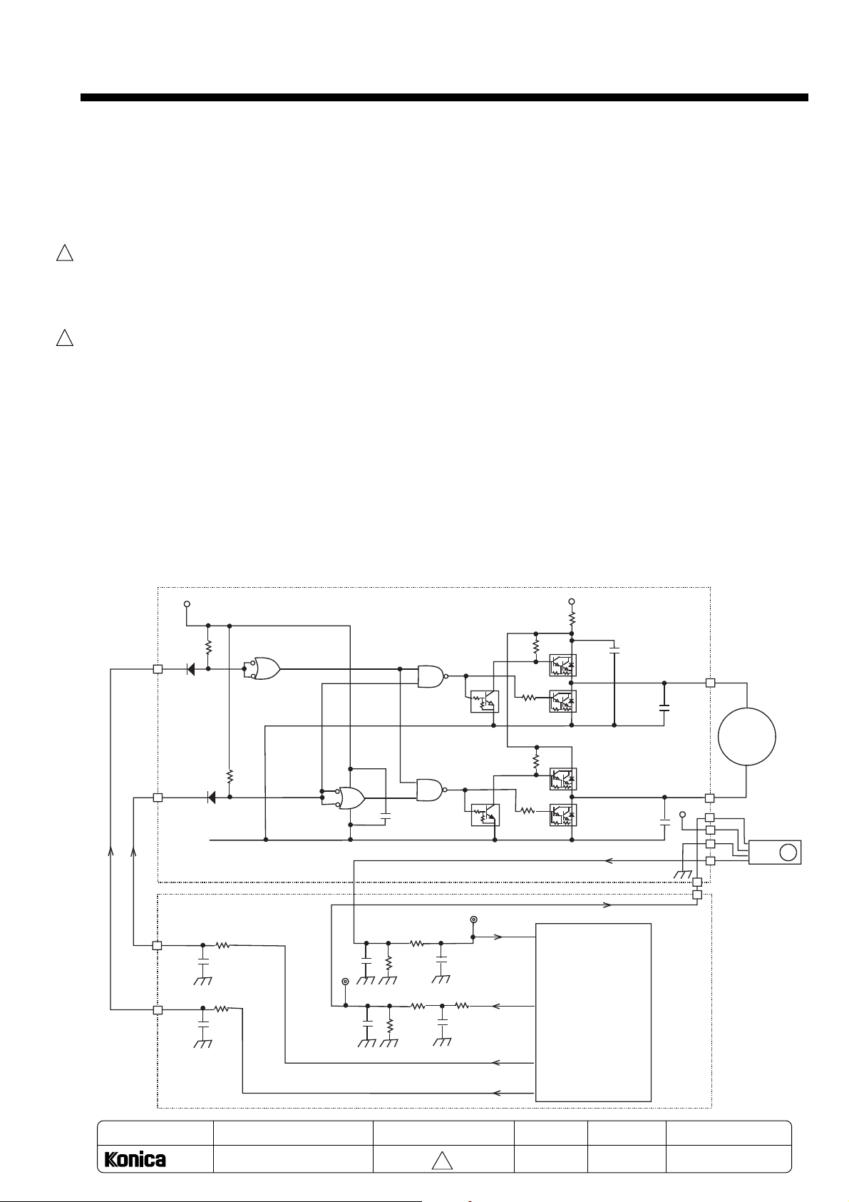
7-1-1. Toner density control
1. Toner density detection
The TNS signal detected by the toner sensor is relayed by the high voltage unit (UNIT HV) and connected to
CN191-20 on the main CB (UNIT MAIN). After the TNS signal is changed to a partial voltage (TNS! signal) by the
registance in the main CB, it is input into the IC121 (CPU) pin No. 77. The TNS! signal can be measured with the
test point (TP103).
2. Toner motor drive control
1
As the toner is consumed and the toner density becomes lighter than the optimum density, the TSM signal is
output (HIGH -> LOW) from the IC121 No. 23 pin. The drive circuit in the high voltage PCB (UNIT HV) is activated to rotate the toner motor (pulse motor) and supply the toner.
Supply time: 3.5 sec.
1
3. Forced toner supply mode
If the toner sensor detects a light density 1% less than the optimum density three times in succession, this unit
will stop the copy operation, and forcibly supply toner. During this mode’s operation, P25 will display (forcibly
supplying toner).time: Max. 250 sec.
When the toner density is recovered (6.5%), the stopped copy job will automatically resume. However, if the
density is not recovered, P25 will blink (toner empty), and after 30 copies, the copy operation will stop.
4. Initialization of developing unit
When the unit’s power is turned on in the unused state (when installed), P26 will light (developer not initialized),
and the standby state will not be entered. This is so that the compensation voltage TNSC signal (analog voltage)
applied on the toner sensor can be calculated beforehand so that the TNS signal will become the reference
voltage in the new developer (unused) state. When the initialization operation (user mode C-51) is carried out,
the detected compensation data will be saved in the main PCB’s EEPROM (IC123). (Note: The developing unit
must be initialized also when it has been replaced.)
Initialization time: 6 min. (3 min. agitation + 3 min. reading & compensation data registration)
+5V
UNIT HV
+24V
CN1261-5
CN191-18
CN191-17
/TSM
TSMCLK
GND24
TSMCLK
/TSM
UNIT MAIN
CI1251B
CI1251A
TP104
CI1251C
CI1251D
Q1255
Q1256
TP103
TNS!
TNSC!
TSMCLK
TSM
77
45
23
+24V
CN1251
1
Toner supply
motor
2
3
4
5
6
CN1261-4
CN191-19
Toner sensor
Q1251
Q1252
Q1253
Q1254
IC121
5
TNM0
TNM1
TNS
TNSC
MODEL
1312
MANUAL
SERVICE HANDBOOK
REVISED EDITION
7-1
1
DATA
May.1999
PAGE
7-1
METHOD
REPLACEMENT
Page 3

Chapter 7 Electricity
7-1-2 Fusing temperature control
The surface temperature of the heat roller is detected with a thermistor, and is kept to a constant optimum temperature (188ºC) by turning the fusing heater ON and OFF with the SSR circuit on the power supply PCB (UNIT
PSU).
1. Temperature detection
1
The temperature detection thermistor is contacted against the surface of the heat roller. The resistance value
changes according to the temperature.
Low temperature (20ºC) : 95KΩ~145KΩ
Optimum temperature (188ºC) : 0.9KΩ~1.0KΩ
The FUTHM signal detected by the thermistor is relayed by the power supply PCB (UNIT PSU), and connected to
CN151-B12 in the main PCB (UNIT MAIN). The signal is changed to a partial pressure (TEMP signal) by the
registance in the main PCB. The TEMP signal is changed into a further partial voltage(FU TEMP signal) by the
registance, and input into the IC121 (CPU) pin No. 76. The TEMP signal is approx. 4.14V at the optimum temperature (standard 188ºC), and can be measured with the test point (TP102).
2. Error detection
The TEMP signal is used also to monitor for thermistor errors. If an overheat (FUOVH) or thermistor open
(FUTHOPN) is detected, the heater power is cut off by the safety circuit. If a fault (hardware circuit fault or software hang up) that causes the fusing heater to remain lit occurs, the thermostat connected in series to the fusing
heater operates and cuts off the heater power.
(F34: High temperature error, F35: Low temperature error, F36: Thermistor error -> Must be released with service
mode 25-47)
3. SSR circuit
If the fusing temperature drops below the optimum temperature (188ºC), the SSR signal (LOW-> HIGH) is output
from the IC121 (CPU) pin No. 32, and reversed (HIGH->LOW) by the IC124. Then, the SSR circuit in the power
supply PCB (UNIT PSU) is driven to light the fusing heater.
MODEL
1312
MANUAL
SERVICE HANDBOOK
REVISED EDITION
7-2
1
DATA
May.1999
PAGE
7-2
METHOD
REPLACEMENT
Page 4

Chapter 7 Electricity
7-1-3. JAM detection
Paper jams are detected with the JAM1 sensor (photo coupler) installed at the paper feed section and the JAM2
sensor (switch) installed at the paper exit section. The JAM1 sensor is set before the slip roller, and also acts as
the manual feed detection sensor.
1. JAM1 sensor
The JAM1 signal (HIGH->LOW when there is paper) output from the JAM1 sensor is relayed by the power supply
PCB (UNIT PSU), and is connected to the main PCB (UNIT MAIN) CN151-B1. It is then input into the IC121
(CPU) pin No. 63.
2. JAM2 sensor
The JAM2 signal (HIGH->LOW when there is paper) output from the JAM2 sensor is relayed by the power supply
PCB (UNIT PSU), and is connected to the main PCB (UNIT MAIN) CN151-B13. It is then input into the IC121
(CPU) pin No. 64.
3. JAM detection conditions
Display code
J11
J12
J16
J31
J32
JAM releasing method: Remove the jammed paper, and then open and close the upper cover.
* After the jam releasing procedure was carried out, J16 may occur again when the paper which was at the paper
feed path was fed. In this case, release the jam again.
* Paper was incorrectly fed from unit standard cassette (upper cassette).
* Paper did not reach the JAM1 sensor within 1.3 sec. after the upper
cassette paper feed solenoid turned ON.
* Paper was incorrectly fed from option cassette feeder (lower cassette).
* Paper did not reach the JAM1 sensor within 3.21 sec. after the lower
cassette paper feed solenoid turned ON.
* There was paper on the JAM1 sensor when the power was turned
ON or the upper cover closed.
* The JAM2 sensor did not turn ON within 2.85 to 3.54 sec. after the
regist clutch turned ON.
* The JAM2 sensor did not turn OFF within 2.85 to 3.54 sec. after the
JAM1 sensor turned OFF.
* There was paper on the JAM2 sensor while waiting.
Detection conditions
Unit operation
* Operation stops after the
previous paper is exited.
* Operation stops after the
previous paper is exited.
* Instantaneous stop
* Fusing heater turns OFF.
* Instantaneous stop
* Fusing heater turns OFF.
* Instantaneous stop
* Fusing heater turns OFF.
7-3
Page 5

Chapter 7 Electricity
7-1-4. Safety circuit
With this unit, the interlock switch and upper cover open switch are turned OFF when the user opens the upper
cover. The AC power for the fusing lamp and exposure lamp, and the DC power (+24) for the high voltage circuit
shown in the circuit diagram and that for the main motor are cut off. The main relay is cut off in the same manner
when an error signal is detected on the main PCB (UNIT MAIN).
1. Exposure lamp error
The exposure lamp lighting signal (AVRERR: this is not an error signal) is detected and regulated its waveform by
the exposure lamp lighting detection circuit on the power supply PCB. The AVRERR signal is connected to the
main PCB (UNIT MAIN) by the CN1031-B16, and monitors whether the lamp is continuously lit (approx. 15 sec.).
If it is detected that the lamp is continuously lit for 15 sec. or more, the main relay is cut off by the AVRERR signal
(LOW-> HIGH).
2. Fusing heater error
When an error signal (FUTHOPN: thermistor open, FUOVH: fusing overheat) is detected with the fusing temperature control circuit, the AVRERR signal (LOW->HIGH) is generated in the same manner as the exposure lamp
error, and the main relay is cut off.
(F34: High temperature error, F35: Low temperature error, F36: Thermistor error -> Must be released with service
mode 25-47)
7-4
Page 6

7-2. Timing chart
7-2-1. A4, TWO COPIES, CASSETTE PAPER FEED (UPPER)
1
Chapter 7 Electricity
Main motor
Main erase lamp
Mirror feed
Mirror return
Mirror HP sensor
Exposure lamp
Side erase lamp
Developer bias
Charging
Transfer
Transfer polarity
Paper feed solenoid(U)
Regist clutch
JAM1 sensor
JAM2 sensor
Fan high-speed
Fan low-speed
Toner supply motor
Total counter
9190
10220
10000
10400
10420
10390
10290
10610
LastMultiFirst
12850
12850
11490
11400
12850
13350
12850
12850
10890
12730
13350
13350
12850 13350
5260
200
200
6610
1650
1670
300
1810
100
200
200
1400
770
300
1880
970
1880
0123456789101112131415161718192021
5440
5460 6530
6630
6510
5430
6390
6550
5330
5930
7280
5260 5730
5650
6840
5930
5040
4230
5130 10090
7770
6840
7-2-2. A4, TWO COPIES, CASSETTE PAPER FEED (LOWER)
1
5630
6440
6840
6860 7930
6830
6730
6440 6910
7050
6440
7330
7910
6860
8910
8450
Main motor
Main erase lamp
Mirror feed
Mirror return
Mirror HP sensor
Exposure lamp
Side erase lamp
Developer bias
Charging
Transfer
Transfer polarity
CF motor
Paper feed solenoid(L)
Regist clutch
JAM1 sensor
JAM2 sensor
200
3050
3070
300
3210
100
200
200
3720
300 3030 3280 9170
300
770
3280
1400
Fan high-speed
Fan low-speed
Toner supply motor
3280
6530 12670
Total counter
11440
9190
9350
9860 13470
9420 15430
9420
9170
9420
LastMultiFirst
12980
12960 14030
13900
12790
12870
13190
12580
11770
15430
15430
15930
15430
15430
15310
15930
15930
15430 15930
MODEL
1312
0123456789101112131415161718192021
MANUAL
REVISED EDITION
DATA
PAGE
METHOD
7-5
SERVICE HANDBOOK
1
May.1999
7-5
REPLACEMENT
Page 7

Chapter 7 Electricity
7-3. Connector list
7-3-1. Main CB (UNIT MAIN)
CN - No.
CN131
CN131
CN131
CN131
CN131
CN131
CN131
CN131
CN131
CN131
CN131
CN131
CN151
CN151
CN151
CN151
CN151
CN151
CN151
CN151
CN151
CN151
CN151
CN151
CN151
CN151
CN151
CN151
CN151
CN151
CN151
CN151
CN151
CN151
CN151
CN151
CN151
CN151
CN151
CN151
CN151
CN151
Pin
1
2
3
4
5
6
7
8
9
10
11
12
A1
A2
A3
A4
A5
A6
A7
A8
A9
A10
A11
A12
A13
A14
A15
A16
B1
B2
B3
B4
B5
B6
B7
B8
B9
B10
B11
B12
B13
B14
Symbol
STBLED
/E2000
VRGND
EXPVR
KEY2
KEY1
VR5V
/LEDLD
LEDCKL
LEDDO
DGND
+5V
/PRC
/PSC
STB5
S24V
GND24
GND24
+24V
DGND
DGND
+5V
+5V
+5V
+5V
/PWR
/EXP
EXPCONT
JAM1
/PE
S24V
S24V
GND24
+24V
+24V
DGND
DGND
+5V
/CSOPNU
FUTHM
JAM2
/MRL
Details
Not used
Not used
Exposure density adjustment VR, analog ground for each key
Exposure density adjustment VR signal
Key switch No. 2 group
Key switch No. 1 group
Exposure density adjustment VR, +5V for each key
LED serial data load signal
LED serial data transfer clock
LED lighting serial data
Digital ground
+5V power supply
Paper regist clutch drive signal
Paper feed solenoid(U) drive signal (Drive at Lo)
Not used
+24V power supply via cover open switch
+24V drive system ground
+24V drive system ground
+24V power supply
Digital ground
Digital ground
+5V power supply
+5V power supply
+5V power supply
+5V power supply
Not used
Exposure lamp lighting signal (Lights at Lo)
Exposure lamp lighting voltage control signal (analog)
JAM1 sensor signal
Upper cassette out of paper signal
+24V power supply via cover open switch
+24V power supply via cover open switch
+24V drive system ground
+24V power supply
+24V power supply
Digital ground
Digital ground
+5V power supply
Not used
Fusing temperature (thermistor) detection signal
JAM2 sensor signal
Main relay ON/OFF signal
IN/OUT
IN
IN
IN
OUT
OUT
OUT
OUT
OUT
OUT
OUT
IN
IN
IN
IN
OUT
Analog signal
Analog signal
Analog signal
Load at LOW
Clock signal
LED lights at HIGH
Drive at LOW
Drive at LOW
Lights at LOW
Analog signal
Paper detected at LOW
HIGH when out of paper
Analog signal
Paper detected at LOW
Relay drive at LOW
Active
Remarks
Measurement not possible
Upper cover open: OFF
Upper cover open: OFF
7-6
Page 8

Chapter 7 Electricity
CN - No.
CN151
CN151
CN152
CN152
CN152
CN152
CN152
CN152
CN152
CN152
CN152
CN152
CN152
CN152
CN152
CN152
CN152
CN161
CN161
CN161
CN161
CN162
CN162
Pin
B15
B16
1
2
3
4
5
6
7
8
9
10
11
12
13
14
15
1
2
3
4
1
2
Symbol
/SSR
EXPERR
S24V
GND24
GND24
GND24
+24V
+24V
+24V
SDHFAN
FSLOCK
FOLOCK1
FAN24
MHP
DGND
DRV5V
SDHTHM
/MMLOCK
/MMST
DRV24V
GND24
/TPC
+24V
Details
SSR ON/OFF signal
Exposure lamp lighting monitor signal
IN/OUT
OUT
IN
S24V with ON/OFF control
(+24V except power save mode)
+24V drive system ground
+24V drive system ground
+24V drive system ground
+24V power supply
+24V power supply
+24V power supply
SDH fan ON/OFF signal
SDH fan lock signal
OP fan lock signal
OP fan drive signal
Mirror home position sensor signal
OUT
IN
IN
OUT
IN
Digital ground
+5V with ON/OFF control
SDH temperature detection (thermistor) signal
Main motor speed control lock signal
24/ Main motor drive signal
Power supply (24V) with ON/FF control and safety circuit
OUT
IN
IN
OUT
OUT
+24V drive system ground
Total paper counter drive signal
OUT
+24V power supply
Active
Fusing heater drive at LOW
Remarks
HIGH when exposure lamp is lit
Upper cover open: OFF
Drive at HIGH
HIGH when locked
(8P, 9P, 15P:
factory option)
HIGH when locked
OP fan drive at +24V
HIGH at set position
+5V when not in power save mode
Analog signal
LOW when locked
Drive at LOW
0V during power save
Upper cover open: OFF
Count up at LOW
CN171
CN171
CN171
CN171
CN171
CN171
CN171
CN171
CN171
CN171
CN171
CN171
CN171
CN171
CN191
CN191
CN191
CN191
CN191
1
2
3
4
5
6
7
8
9
10
11
12
13
14
1
2
3
4
5
/CSOPNL
DGND
+5V
/LPE
DGND
DGND
+5V
PTM
/LMST
GND24
+24V
+24V
/LPSC
NC
/DRUM
/TSE
/GRID
/HVCC
/HVTP
Lower cassette not mounted signal
Digital ground
+5V power supply
Lower cassette out of paper signal
Digital ground
Digital ground
+5V power supply
Cassette feeder paper feed motor clock
Cassette feeder paper feed motor ON/OFF signal
OUT
OUT
+24V drive system ground
+24V power supply
+24V power supply
Paper feed solenoid (L)
OUT
Not connected
Drum unit not mounted detection signal
IN
Not used
GRID terminal ON/OFF signal
CC terminal ON/OFF signal
TC polarity changeover signal
OUT
OUT
OUT
HIGH when no cassette is mounted
HIGH when out of paper
Clock signal
Measurement not possible
Drive at HIGH
Drive at LOW
HIGH when on mounted
GRID output at LOW
CC output at LOW
TC + polarity at LOW
7-7
Page 9

Chapter 7 Electricity
CN - No.
CN191
CN191
CN191
CN191
CN191
CN191
CN191
CN191
CN191
CN191
CN191
CN191
CN191
CN191
CN191
CN191
CN191
Pin
6
7
8
9
10
11
12
13
14
15
16
17
18
19
20
21
22
Symbol
/HVTC
/LMB
/LMA
LMB
LMA
/SMB
/SMA
SMB
SMA
LHP
TRAYS
/TSM
TSMCLK
TNSC
TNS
DGND
AE
Details
TC terminal ON/OFF signal
Lens motor drive excitation signal (/B phase)
Lens motor drive excitation signal (/A phase)
Lens motor drive excitation signal (/B phase)
Lens motor drive excitation signal (/A phase)
Mirror motor drive excitation signal (/B phase)
Mirror motor drive excitation signal (/A phase)
Mirror motor drive excitation signal (/B phase)
Mirror motor drive excitation signal (/A phase)
Lens home position sensor signal
IN/OUT
OUT
OUT
OUT
OUT
OUT
OUT
OUT
OUT
OUT
IN
Not used
Toner motor drive signal
Toner motor drive clock
Signal for toner sensor output adjustment
Toner sensor output signal
OUT
OUT
OUT
IN
Digital ground
Not used
Active
TC output at LOW
Clock signal
Clock signal
Clock signal
Clock signal
Clock signal
Clock signal
Clock signal
Clock signal
HIGH at set position
ON at LOW
60Hz pulse
Analog signal
Analog signal
Remarks
Measurement not possible
Measurement not possible
Measurement not possible
Measurement not possible
Measurement not possible
Measurement not possible
Measurement not possible
Measurement not possible
Voltage rises at
low density
CN192
CN192
CN192
CN192
CN192
CN192
CN192
CN192
CN192
CN192
CN192
CN192
CN192
CN192
CN192
CN192
CN192
CN192
1
2
3
4
5
6
7
8
9
10
11
12
13
14
15
16
17
18
CCL
/SER6
/SER5
/SER4
/SER3
/SER2
/SER1
/SER0
/AMB
/AMA
AMB
AMA
MRM
SDHPC
SDHOPN
/CS3
/CS2
/CS1
Main erase lamp drive signal
Side erase lamp drive signal(D56,D66)
Side erase lamp drive signal(D55,D65)
Side erase lamp drive signal(D54,D64)
Side erase lamp drive signal(D53,D63)
Side erase lamp drive signal(D52,D62)
Side erase lamp drive signal(D51,D61)
Side erase lamp drive signal
OUT
OUT
OUT
OUT
OUT
OUT
OUT
OUT
(D71 to D78,D81 to D88)
SDH motor drive excitation signal (/B phase)
SDH motor drive excitation signal (/A phase)
SDH motor drive excitation signal (/B phase)
SDH motor drive excitation signal (/A phase)
Mirror motor, SDH motor exciting current changeover signal
SDH paper feed clutch drive signal
SDH open detection sensor signal
SDH B4 size detection sensor signal
SDH document regist sensor signal
SDH no original detection sensor signal
OUT
OUT
OUT
OUT
OUT
OUT
IN
IN
IN
IN
Drive at +24V
Lights at LOW
Lights at LOW
Lights at LOW
Lights at LOW
Lights at LOW
Lights at LOW
Lights at LOW
(9 to 12P, 14 to 18P
: factory option)
Clock signal
Clock signal
Clock signal
Clock signal
Measurement not possible
Measurement not possible
Measurement not possible
Measurement not possible
Low current at HIGH
Clutch ON at HIGH
HIGH at open
LOW at B4 detection
LOW when original feed
LOW when original is detected
7-8
Page 10

7-3-2. High voltage unit (UNIT HV)
Chapter 7 Electricity
CN - No.
CN1201
CN1201
CN1201
CN1201
CN1201
CN1201
CN1211
CN1211
CN1211
CN1211
CN1211
CN1231
CN1231
CN1231
CN1231
CN1231
CN1231
CN1231
CN1231
CN1231
CN1231
CN1251
CN1251
CN1251
CN1251
CN1251
CN1251
CN1261
CN1261
CN1261
CN1261
CN1261
CN1261
CN1261
CN1261
CN1261
CN1261
CN1261
CN1261
CN1261
CN1261
Pin Symbol Details
1
2
3
4
5
6
1
2
3
4
5
1
2
3
4
5
6
7
8
9
10
1
2
3
4
5
6
1
2
3
4
5
6
7
8
9
10
11
12
13
14
LMOA
LMOB
/LMOA
/LMOB
LM24V
LM24V
SMOA
SMOB
/SMOA
/SMOB
SM24V
+24V
/SDHPC
+24V
/SDHPC
AMOA
AMOB
/AMOA
/AMOB
AM24V
AM24V
TNM0
TNM1
TNSC
+24V
DGND
TNS
AE
DGND
TNS
TNSC
TSMCLK
/TSM
TRAYS
LHP
SMA
SMB
/SMA
/SMB
LMA
LMB
Lens motor drive excitation signal (/A phase)Output
Lens motor drive excitation signal (/B phase)Output
Lens motor drive excitation signal (/A phase)Output
Lens motor drive excitation signal (/B phase)Output
Lens motor power supply
Lens motor power supply
Mirror motor drive excitation signal (/A phase)Output
Mirror motor drive excitation signal (/B phase)Output
Mirror motor drive excitation signal (/A phase)Output
Mirror motor drive excitation signal (/B phase)Output
Scanner motor power supply
+24V power supply
SDH shutter solenoid output
+24V power supply
SDH paper feed clutch output
SDH motor drive excitation signal (/A phase)Output
SDH motor drive excitation signal (/B phase)Output
SDH motor drive excitation signal (/A phase)Output
SDH motor drive excitation signal (/B phase)Output
SDH motor power supply
SDH motor power supply
Toner motor drive power supply output
Toner motor drive power supply output
Signal for toner sensor output adjustment
+24V power supply
Digital ground
Toner sensor output signal
Not used
Not used
Toner sensor output signal
Signal for toner sensor output adjustment
Toner motor drive clock
Toner motor drive signal
Not used
Lens home position sensor signal
Mirror motor drive excitation signal (/A phase)
Mirror motor drive excitation signal (/B phase)
Mirror motor drive excitation signal (/A phase)
Mirror motor drive excitation signal (/B phase)
Lens motor drive excitation signal (/A phase)
Lens motor drive excitation signal (/B phase)
IN/OUT
OUT
OUT
OUT
OUT
OUT
OUT
OUT
OUT
OUT
OUT
OUT
OUT
OUT
OUT
OUT
IN
IN
OUT
OUT
OUT
IN
OUT
OUT
OUT
OUT
OUT
OUT
Active Remarks
Clock signal
Clock signal
Clock signal
Clock signal
Clock signal
Clock signal
Clock signal
Clock signal
Measurement not possible
Measurement not possible
Measurement not possible
Measurement not possible
Measurement not possible
Measurement not possible
Measurement not possible
Measurement not possible
(factory option)
ON at LOW
ON at LOW
Clock signal
Clock signal
Clock signal
Clock signal
Measurement not possible
Measurement not possible
Measurement not possible
Measurement not possible
60Hz pulse
60Hz pulse
Analog signal
Analog signal
Voltage rises at
low density
Analog signal
Voltage rises at
low density
Analog signal
60Hz pulse
Measurement not possible
ON at LOW
HIGH at set position
Clock signal
Clock signal
Clock signal
Clock signal
Clock signal
Clock signal
Measurement not possible
Measurement not possible
Measurement not possible
Measurement not possible
Measurement not possible
Measurement not possible
7-9
Page 11

Chapter 7 Electricity
CN - No.
CN1261
CN1261
CN1261
CN1261
CN1261
CN1261
CN1261
CN1261
CN1262
CN1262
CN1262
CN1262
CN1262
CN1262
CN1262
CN1262
CN1262
CN1262
CN1262
CN1262
CN1262
CN1262
CN1262
CN1262
CN1262
CN1262
CN1263
CN1263
CN1263
CN1263
CN1263
CN1263
CN1263
CN1263
CN1263
CN1263
CN1263
CN1263
CN1263
CN1263
CN1263
Pin Symbol
/LMA
15
/LMB
16
/HVTC
17
/HVTP
18
/HVCC
19
/GRID
20
/TSE
21
/DRUM
22
/CS1
1
/CS2
2
/CS3
3
SDHOPN
4
SDHPC
5
MRM
6
AMA
7
AMB
8
/AMA
9
/AMB
10
/SER0
11
/SER1
12
/SER2
13
/SER3
14
/SER4
15
/SER5
16
/SER6
17
CCL
18
SDHTHM
1
DRV5V
2
DGND
3
MHP
4
FAN24
5
FOLOCK1
6
FSLOCK
7
SDHFAN
8
+24V
9
+24V
10
+24V
11
GND24
12
GND24
13
GND24
14
S24V
15
Details
Lens motor drive excitation signal (/A phase)
Lens motor drive excitation signal (/B phase)
TC terminal ON/OF signal
TC polarity changeover signal
CC terminal ON/OF signal
GRID terminal ON/OF signal
IN/OUT
OUT
OUT
OUT
OUT
OUT
OUT
Not used
Drum unit not mounted detection signal
SDH no original detection sensor signal
SDH document regist sensor signal
SDH B4 size detection sensor signal
SDH open detection sensor signal
SDH paper feed clutch drive signal
Mirror motor, SDH motor exciting current changeover signal
SDH motor drive excitation signal (/A phase)
SDH motor drive excitation signal (/B phase)
SDH motor drive excitation signal (/A phase)
SDH motor drive excitation signal (/B phase)
Side erase lamp drive signal
IN
IN
IN
IN
IN
OUT
OUT
OUT
OUT
OUT
OUT
OUT
(D71 to D78,D81 to D88)
Side erase lamp drive signal(D56,D66)
Side erase lamp drive signal(D55,D65)
Side erase lamp drive signal(D54,D64)
Side erase lamp drive signal(D53,D63)
Side erase lamp drive signal(D52,D62)
Side erase lamp drive signal(D51,D61)
Main erase lamp drive signal
SDH temperature detection (thermistor) signal
+5V with ON/OFF control
OUT
OUT
OUT
OUT
OUT
OUT
OUT
IN
OUT
Digital ground
Mirror home position sensor signal
IN
OP fan drive signal
OP fan lock signal
SDH fan lock signal
SDH fan ON/OFF signal
IN
IN
OUT
+24V power supply
+24V power supply
+24V power supply
+24V drive system ground
+24V drive system ground
+24V drive system ground
+24V power supply via cover open switch
Active
Clock signal
Clock signal
Measurement not possible
Measurement not possible
TC output at LOW
TC + polarity at LOW
TC output at LOW
TC output at LOW
HIGH when not mounted
LOW when original is
detected
LOW when original feed
(1 to 5P: factory
option)
LOW at B4 detection
HIGH when open
Clutch ON at HIGH
Small current at HIGH
Clock signal
Clock signal
Clock signal
Clock signal
Measurement not possible (pulse wave)
Measurement not possible (pulse wave)
Measurement not possible (pulse wave)
Measurement not possible (pulse wave)
Lights at LOW
Lights at LOW
Lights at LOW
Lights at LOW
Lights at LOW
Lights at LOW
Lights at LOW
Analog signal
+5V when not in
(1 to 5P: factory
option)
power save mode
HIGH at set position
OP fan drive at +24V
HIGH when locked
HIGH when locked
Drive at HIGH
Upper cover open: OFF
Remarks
7-10
Page 12

CN - No.
Symbol Active
Pin
Details
IN/OUT
Chapter 7 Electricity
Remarks
CN1271
CN1271
CN1271
CN1271
CN1272
CN1272
CN1272
CN1273
CN1273
CN1273
CN1274
CN1274
CN1275
CN1275
CN1275
CN1276
CN1276
CN1276
CN1276
CN1276
CN1276
CN1276
CN1276
CN1277
CN1277
CN1277
CN1278
CN1278
CN1281
CN1281
CN1281
CN1281
CN1281
CN1281
CN1281
CN1281
CN1281
CN1282
CN1282
CN1282
1
2
3
4
1
2
3
1
2
3
1
2
1
2
3
1
2
3
4
5
6
7
8
1
2
3
1
2
1
2
3
4
5
6
7
8
9
1
2
3
+5V
LHP
DGND
NC
+5V
MHP
DGND
GND24
FOLOCK1
FAN24
+5V
SDHTHM
+5V
AE
DGND
+24V
SER0
SER1
SER2
SER3
SER4
SER5
SER6
GND24
FSLOCK
SFAN24
+24V
/CCL
/CS1
DGND
+5V
/CS2
DGND
/CS3
DGND
SDHOPN
DGND
GND24
FOLOCK2
FAN24
+5V power supply
Lens home position sensor signal
IN
Digital ground
Not connected
+5V power supply
Mirror home position sensor signal
IN
Digital ground
Ground
OP fan 1 lock signal
OP fan drive signal
IN
OUT
+5V power supply
SDH temperature detection (thermistor) signal
IN
Not used
Not used
Not used
+24V power supply
Side erase lamp drive signal
OUT
(D71~D78,D81~D88)
Side erase lamp drive signal(D51,D61)
Side erase lamp drive signal(D52,D62)
Side erase lamp drive signal(D53,D63)
Side erase lamp drive signal(D54,D64)
Side erase lamp drive signal(D55,D65)
Side erase lamp drive signal(D56,D66)
OUT
OUT
OUT
OUT
OUT
OUT
+24V drive system ground
SDH fan lock signal
IN
SDH fan power supply output
+24V power supply
Main erase lamp drive signal
SDH no original detection sensor signal
OUT
IN
Digital ground
+5V power supply
SDH document regist sensor signal
IN
Digital ground
SDH B4 size detection sensor signal
IN
Digital ground
SDH open detection sensor signal
IN
Digital ground
Ground
OP fan 2 lock signal
IN
OP fan 2 power supply output
HIGH at set position
HIGH at set position
HIGH when locked
OP fan drive at +24V
(Factory option)
Analog signal
Lights at LOW
Lights at LOW
Lights at LOW
Lights at LOW
Lights at LOW
Lights at LOW
Lights at LOW
(Factory option)
HIGH when locked
SDH fan drive at +24V
Lights at LOW
LOW when original is detected
(Factory option)
Detected when LOW
LOW when original feed
LOW at B4 detection
HIGH when open
HIGH when locked
7-11
Page 13

Chapter 7 Electricity
7-3-3. Power supply board (UNIT PSU)
CN - No.
CN1001
CN1001
CN1001
CN1002
CN1002
CN1011
CN1011
CN1031
CN1031
CN1031
CN1031
CN1031
CN1031
CN1031
CN1031
CN1031
CN1031
CN1031
CN1031
CN1031
CN1031
CN1031
CN1031
CN1031
CN1031
CN1031
CN1031
CN1031
CN1031
CN1031
CN1031
CN1031
CN1031
CN1031
CN1031
CN1031
CN1031
CN1031
CN1031
CN1032
CN1032
CN1032
CN1032
Pin
1
2
3
1
2
1
2
A1
A2
A3
A4
A5
A6
A7
A8
A9
A10
A11
A12
A13
A14
A15
A16
B1
B2
B3
B4
B5
B6
B7
B8
B9
B10
B11
B12
B13
B14
B15
B16
1
2
1
2
Symbol
AC-L
NC
AC-N
FU-L
FU-N
EXP-L
EXP-N
/PRC
/PSC
STB5
S24V
GND24
GND24
+24V
DGND
DGND
+5V
+5V
+5V
+5V
/PWR
/EXP
EXPCONT
JAM1
/PE
S24V
S24V
GND24
+24V
+24V
DGND
DGND
+5V
/CSOPNU
FUTHM
JAM2
/MRL
/SSR
EXPERR
+24V
/PSC
+24V
/PRC
Details
Power supply input(L)
IN/OUT
IN
AC primary circuit
Not connected
Power supply input(N)
Fusing heater output(L)
Fusing heater output(N)
Exposure lamp output(L)
Exposure lamp output(N)
Paper regist clutch drive signal
Paper feed solenoid(U) drive signal (Drive at Lo)
IN
OUT
OUT
OUT
OUT
OUT
OUT
AC primary circuit
AC primary circuit
AC primary circuit
AC primary circuit
AC primary circuit
Drive at LOW
Drive at LOW
Not used
+24V power supply via cover open switch
+24V drive system ground
+24V drive system ground
+24V power supply
Digital ground
Digital ground
+5V power supply
+5V power supply
+5V power supply
+5V power supply
Not used
Exposure lamp lighting signal (Lights at Lo)
Exposure lamp lighting voltage control signal (analog)
JAM1 sensor signal
OUT
OUT
IN
Lights at LOW
Analog signal
Paper detected at LOW
Not used
+24V power supply via cover open switch
+24V power supply via cover open switch
+24V power supply
+24V power supply
+24V power supply
Digital ground
Digital ground
+5V power supply
Standard cassette not mounted signal
Fusing temperature (thermistor) detection signal
JAM1 sensor signal
Main relay ON/OFF signal
SSR ON/OFF signal
Exposure lamp lighting monitor signal
IN
IN
IN
OUT
OUT
IN
No cassette mounted at HIGH
Analog signal
Paper detected at LOW
Relay drive at LOW
Fusing heater drive at LOW
HIGH when exposure lamp is lit
+24V power supply
Paper feed solenoid(U) drive signal
OUT
Drive at LOW
+24V power supply
Regist clutch drive signal
OUT
Drive at LOW
Active
Remarks
Upper cover open: OFF
Upper cover open: OFF
7-12
Page 14

Chapter 7 Electricity
CN - No.
CN1034
CN1034
CN1034
CN1035
CN1035
CN1035
CN1036
CN1036
CN1037
CN1037
CN1038
CN1038
CN1038
Pin Symbol Details
1
2
3
1
2
3
1
2
1
2
1
2
3
LEDJ1
JAM1
DGND
LEDPE
/PE
DGND
+24V
S24V
+5V
FUTHM
NC
JAM2
DGND
7-4. IC list
PCB Location No.
IN/OUT
+5V power supply for JAM1 sensor
JAM1 sensor signal
Digital ground
+5V power supply for PE sensor
Upper cassette out of paper signal
Digital ground
+24V power supply
+24V power supply via cover open switch
+5V power supply
Fusing temperature (thermistor) detection signal
Not connected
JAM2 sensor signal
Digital ground
Part name/type
IN
OUT
IN
IN
IN
Active Remarks
Paper detected at LOW
HIGH when out of paper
Upper cover open: OFF
1Analog signal
Paper detected at LOW
Application
UNIT PSU
UNIT PSU
UNIT PSU
UNIT PSU
UNIT OP
UNIT OP
UNIT MAIN
UNIT MAIN
UNIT MAIN
UNIT MAIN
UNIT MAIN
UNIT MAIN
UNIT MAIN
UNIT MAIN
UNIT MAIN
UNIT MAIN
UNIT MAIN
UNIT MAIN
UNIT MAIN
UNIT MAIN
UNIT HV
UNIT HV
UNIT HV
UNIT HV
UNIT HV
IC1031
IC1051
IC1071
IC1081
IC751
IC770 IC780
IC121
IC122
IC123
IC124
IC125
IC126
IC141
IC151
IC152
IC181 IC182
IC191
IC192 IC193
IC194
IC195
IC1121
IC1122
IC1171
IC1211
IC1251
LA6358NM-TP-T1
MC33262P
UPC1093T-T1
MC34063AP1
LC7932M-TE-R
LC7933M-TE-R
UPD78054FGC
M51953BFP-600C
S-29130AFJ-TB
TD62503F-TP1
TD62003AF-TP1
TC7W02F-TE12L
LA6393M-TP-T1
HD74HC132FP-TR
TC7W02F-TE12L
HD74HC244FP-TR
HD74HC244FP-TR
HD74HC175FP-T
HD74HC175FP-T
TD62503F-TP1
MC33262P
TA78L012AP
LA6082M-TP-T1
MTD1120F
HD74HC00FP-TR
Operation amplifier (for exposure lamp lighting control (AVR))
Switching power control
Reference voltage IC (switching power section)
DC-DC converter IC (+5V power supply)
Serial-parallel driver (for each LED lighting)
Serial driver (for 7-segment LED lighting)
CPU
Reset IC
EEPROM (for electronic counter, setting, adjustment data storage)
Transistor array (for high voltage, exposure and fusing drive)
Transistor array (clutch, solenoid main relay drive)
NOR gate (for main relay control signal)
Comparator (for fusing temperature error detection)
NAND gate (for exposure lamp lighting error detection)
OR gate (for exposure lamp lighting error detection)
Line buffer (stepping motor exciting output)
Line buffer (optical section sensor input selector)
D-TYPE FF (Side erase lamp, mirror motor control output)
D-TYPE FF (SDH clutch, SDH fan control output)
Transistor array (for side erase lamp drive)
Switching power control IC (charge, bias output)
12V 3-terminal regulator
Operation amplifier (for transfer output control)
Stepping motor set current drive driver (mirror scanner)
NAND gate (toner motor section)
7-13
Page 15

Chapter 7 Electricity
7-5. Test points and VR list
Location
UNIT MAIN
UNIT MAIN
UNIT MAIN
UNIT MAIN
UNIT MAIN
UNIT MAIN
UNIT MAIN
UNIT MAIN
UNIT MAIN
UNIT PSU
UNIT OP
Test point
TP101
TP102
TP103
TP104
TP105
TP106
TP107
TP108
TP109
VR1031
VR723
Symbol
DGND
TEMP
TNS!
TNSC
EXPCNT
EXRVR
KEY1
KEY2
AE!
-
-
7-6. Electrical parts layout drawing
7-6-1. PCB, lamp (heater), fuse (rating)
High voltage unit
(UNIT HV)
Main CB
(UNIT MAIN)
Power supply board
(UNIT PSU)
Fuse PCB
(UNIT FUSE)
Side erase lamp
Details
Remarks
Digital ground
Fusing temperature detection signal
Toner sensor output voltage
Toner sensor control voltage
Exposure lamp lighting voltage control signal (analog)
Exposure lamp lighting voltage adjustment input (analog)
Key switches No. 1 group (analog)
Key switches No. 2 group (analog)
Not used
For exposure voltage output adjustment
For exposure voltage output adjustment
Temperature fuse 128 C
Main erase lamp
1
Refer to page 7-2.
Refer to page 7-1.
Refer to page 7-1.
For factory use
For factory use
For factory use
For factory use
-
For factory adjustment (cannot be used)
For user operations (operation panel)
(For 120V machine is one fuse at front side)
Exposure lamp
80V 220W (for 120V)
160V 220W (for 220V to 240V)
Operation PCB
(UNIT OP)
Cassette heater
fuse
250V 4A
Main fuse
125V 10A(for 120V)
250V 6.3A
(for 220 to 240V)
Main cassette
dehumidification heater
fuse 250V 1.6A
Power supply board main fuse
125V 3.15A(for 120V)
250V 1.6A(for 220 to 240V)
Cassette feeder (option)
Dehumidification heater
Fuse 250V 1.6A
MODEL
1312
SERVICE HANDBOOK
MANUAL
Cassette feeder motor driver PCB
(UNIT MOTOR DRIVER)
REVISED EDITION
DATA
7-14
1
May.1999
1
Thermostat
150 C(For 120V
machine is one
thermostat at rear
side)
Fusing heater
120V 800W (for 120V)
230V 800W
(for 220 to 240V)
Main cassette
dehumidification heater
Cassette feeder (option)
dehumidification heater
PAGE
7-14
METHOD
REPLACEMENT
Page 16

Chapter 7 Electricity
7-6-2. Clutches (solenoid) and motors
SDH paper feed clutch
Lens drive motor
Mirror scan motor
Main motor
Toner supply motor
Regist clutch
Paper feed
solenoid(U)
Cassette feeder
paper feed motor
Paper feed solenoid(L)
SDH shutter solenoid
SDH paper feed motor
SDH cooling fan
OP cooling fan
7-6-3. Sensors and switches
1
SDH original detection sensor
Mirror home position sensor
Interlock switch
Main switch
JAM1 sensor
SDH original read
detection sensor
SDH thermistor
SDH cover open
detection sensor
Operation keys
Lens home
position sensor
JAM2 sensor
MODEL
PE sensor
1312
MANUAL
SERVICE HANDBOOK
Toner sensor
REVISED EDITION
7-15
1
Recycle switch
DATA
May.1999
Thermistor
PAGE
7-15
METHOD
REPLACEMENT
 Loading...