CD MECHANISM ASSY
X92-4590-0x
SERVICE MANUAL
DESCRIPTION MECHANISM
X92-4590-00 (DXM-6510W)
X92-4590-01 (DXM-6511W)
X92-4590-02 (DXM-6512W)
X92-4590-03 (DXM-6513W)
CONSTRUCTION OF MAJOR PARTS
© 2002-3 PRINTED IN JAPAN
B51-7933-00 (N) 3412
MP START : Nov. 2001
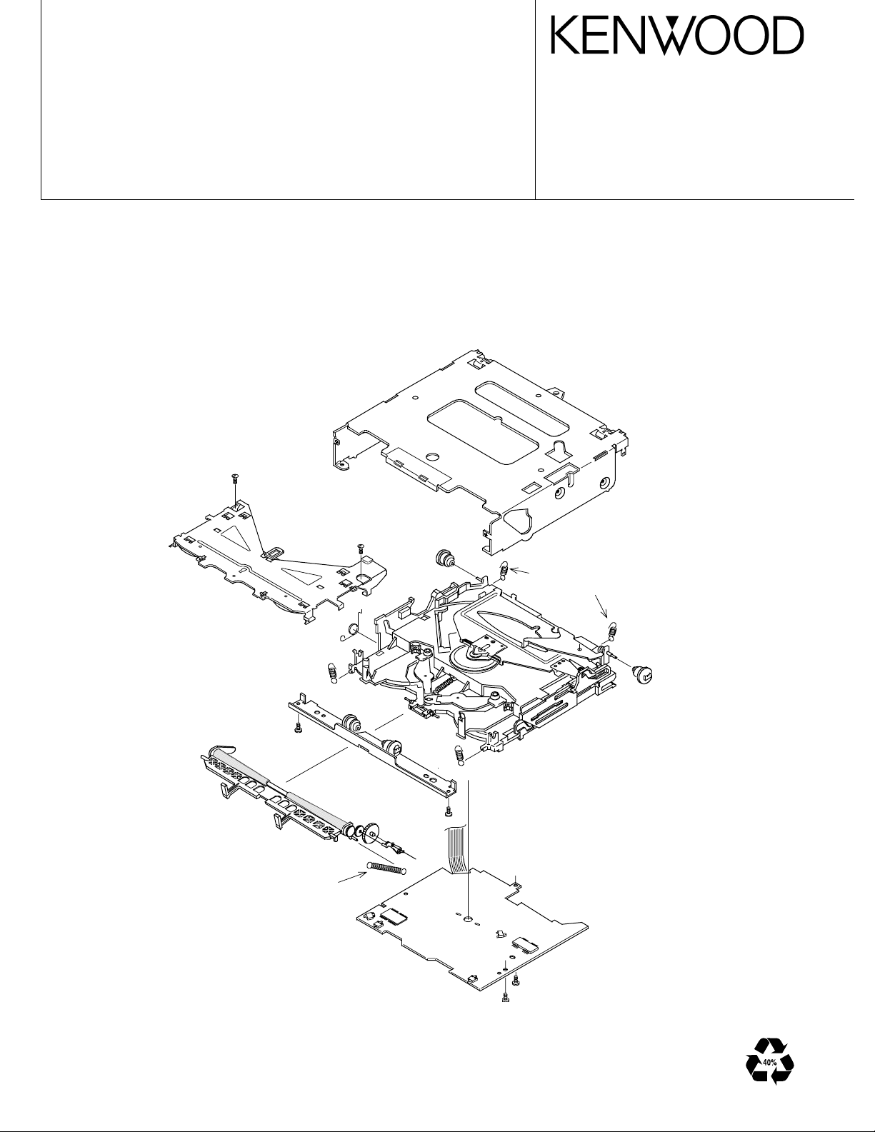
outer-chassis
disc guide assy
damper bracket
roller lever assy
dumper (X4)
floating spring (X4)
traverse chassis assy
roller spring
Mecha PCB
X92-4590-0x
Pick-Up
7
B
A
E
C
D
Tr Coil
Fo Coil
Spindle Motor
Loading & Sled
Motor
F
Q2
APC
2
2
IC4
2
Motor Driver
2
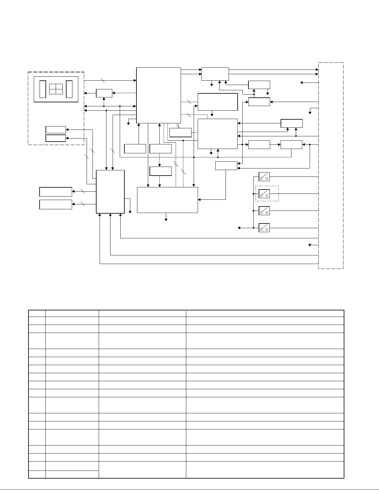
BLOCK DIAGRAM
Mother Board
IC10
1Chip IC
Servo Processor
+
RF Amp
+
MP3 Decorder
Vref
6
D.GND
X2
Clock
4
16.93MHz
16.93MHz
S.GND
X3
IC9
IC8
IC7
Clock
24.57MHz
Buffer
WMA Decorder
D.GND
Level
Shifter
9
IC12
LPF
A.GND
IC11
30
6
16
DRAM
D.GND
IC5 Q1 D.GND
MI-COM
D.GND
IC3
/PON
D2.5V AVR
D.GND Los SW
IC6
A3.3V
A3.3V AVR
A.8V
Q4,5
SW5V
Q3 IC2
A.8V SW
D3.3V SWPON
A.GND
S3
S4
S2
S1
SW5V SW
0-01 Only
R-ch
L-ch
A.GND
A.+8V
D.GND
Bu.+5V
D4.7VD3.3V AVR
Loe/Lim SW
8Eje SW
12Eje SW
COMPONENTS DESCRIPTION
● CD PLAYER UNIT (X32-5350-0x)
Ref. No.
IC2 L88MS33T D3.3V AVR Power supply for the pickup, IC5, IC8-10 and IC11
IC3 UPC3025 D2.5V AVR Power supply for IC8
IC4 BA5824FP 4CH BTL driver
IC5 703030BYGF-M01 Mecha. control MI-COM.
IC6 TAR5S33 A3.3V AVR Power supply for DAC, LPF operational reference voltage
IC7 TC7MET541AKF Level shifting (3.3VÆ5V) Buffer and logic level conversion from IC10 to IC5
IC8 UPD61002GC-E01 WMA decoder
IC9 TC7SHU04FU Clock buffer for WMA
IC10 UPD63760GJ RF amplifier+CD DSP+MP3 decoder
IC11
IC12 NJM4580V Low pass filter 2nd low pass filter for audio signals
IC13 HD74LV14AT Schmitt trigger for WMA
Q1 DTA143EK SW5V SW
Q2 MCH6101 APC LD power control
Q3 DTC124EUA D3.3V SW When PON (13pin) goes Hi, Q3 is turned on, and IC2 is working.
Q4 DTA143XUA
Q5 DTC124EUA supplied to IC6 and IC12.
2
Component Name Application/Function Operation/Condition/Compatibility
Focusing coil, tracking coil, spindle motor and sled motor driver,
disc loading and eject operation.
IS41LV16257 or
MSM51V4265EP70
4M bit DRAM For data buffer
When PON (14pin) goes Lo, Q1 is turned on, and SW5V is supplied
to IC7 and AVREF (73PIN).
A.8V SW
When PON (13pin) goes Hi, Q4 and Q5 are turned on, and A.8V is
S7.5V
S.GND
Lo/Ej
Motor
X92-4590-0x
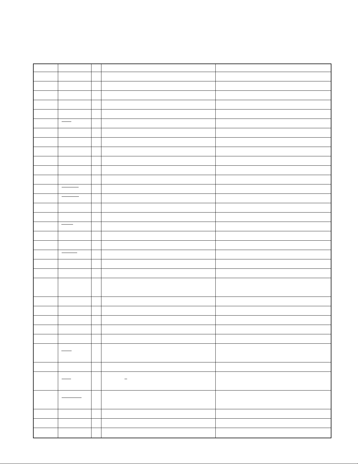
MICROCOMPUTER’S TERMINAL DESCRIPTION
● IC5 (CD PLAYER UNIT : X32-5350-0x)
Pin No. Pin Name I/O Description Processing Operation
1~8 NC O Not used (N.C.)
9 EVDD - Positive power supply connection terminal Connected to BU 5V lines.
10 EVSS - Ground connection terminal Connected to GND lines.
11,12 NC O Not used (N.C.)
13 PON O Power ON/OFF control terminal Lo: Power OFF, Hi: Power ON
14 PON O Power ON/OFF control terminal Lo: Power ON, Hi: Power OFF
15 LOE/LIM SW I Down limit SW detection terminal HiÆLo: Pickup most inner position detected
16 8EJE SW I 8cm disc detection SW input Not used (Pull down to GND lines)
17 LOS SW I Loading start detection SW input Not used (Pull down to GND lines)
18 12EJE SW I 12cm disc detection SW input Not used (Pull down to GND lines)
19,20 NC O Not used (N.C.)
21 VPP - FLUSH write terminal Not used (Connected to GND lines)
22 MUTE L O Lch. Audio muting request output Lo: Muting ON requested, Hi: Muting OFF requested
23 MUTE R O Rch. Audio muting request output Lo: Muting ON requested, Hi: Muting OFF requested
24~28 NC O Not used (N.C.)
29 EFLG I WMA error detection input Lo: No ERROR, Hi: ERROR detected
30 WAIT I Wait control signal detection input
31 FOK I Focusing condition detection input Lo: Focusing NG, Hi: Focusing OK
32,33 NC O Not used (N.C.)
34 RESET I Reset terminal Lo: Reset, Hi: Normal operation
35 XT1 I Sub clock resonator connection terminal Not used (Pull down to GND lines)
36 XT2 - Sub clock resonator connection terminal Not used (N.C.)
37 REGC -
38 X2 - Main clock resonator connection terminal
39 X1 I Main clock resonator connection terminal
40 VSS - Ground connection terminal Connected to GND lines.
41 VDD - Positive power supply connection terminal Connected to B U 5V lines.
42 NC O Not used (N.C.)
43 WRL O Multiplex WRITE signal output
44 NC O Not used (N.C.)
45 R/W O Multiplex R/W signal output
46 DSTB/RD O Multiplex DSTB/RD signal output
47 ASTB O Multiplex ASTB signal output
48,49 NC O Not used (N.C.)
50~57 AD0~AD7 I/O Multiplex address/data bus
Capacitor connection terminal for regulator inside
microprocessor
Lo: Write signal for IC10
Not used for IC8
Not used for IC10
Lo: Read signal, Hi: Write signal for IC8
Lo: Read signal for IC10
Lo: Data strobe signal for IC8
3
X92-4590-0x
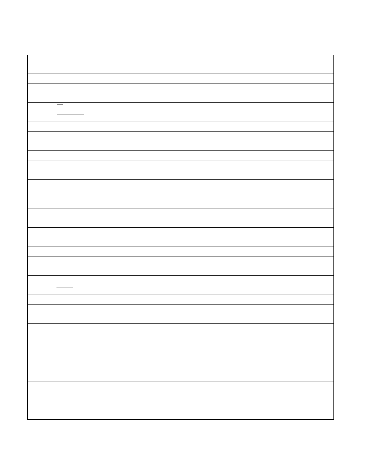
MICROCOMPUTER’S TERMINAL DESCRIPTION
Pin No. Pin Name I/O Description Processing Operation
58 BVDD 59 BVSS - Bus interface ground connection terminal Connected to GND lines.
60~67 AD8~AD15 I/O Multiplex address/data bus
68 HCSB O Chip select control output to IC8 Lo: Chip select ON
69 CS O Chip select control output to IC10 Lo: Chip select ON
70 DSP RESET O DSP reset output Lo: Reset, Hi: Normal operation
71 REQ I Data transfer request input
72 DBBWRDY0 I DBB00 register write permission input
73 DBBRRDY0 I DBB00 register read permission input
74 AVDD 75 AVSS - A/D converter ground connection terminal Connected to GND lines.
76 AVREF I A/D converter reference voltage input terminal Connected to SW 5V lines.
77~80 NC I Not used (Connected to GND lines)
81 HOT I Temperature change detection input
82 M-CONT I Not used (Connected to GND lines)
83 WMA I WMA adaptation selection input Lo: WMA not adapted, Hi: WMA adapted
84 NC I Not used (Connected to GND lines)
85 ASEL I Audio output polarity selection input Lo: Non-inverted output, Hi: Inverted output
86 DASC I Shock proof method selection input Lo: Shock proof OFF, Hi: Shock proof ON
87 TEST2 I Test terminal 2 Not used (Pull down to GND lines)
88 TEST3 I Test terminal 3 Not used (Pull down to GND lines)
89 NC O Not used (N.C.)
90 MSTOP I MECHA. Stop interrupt input Lo: Stop, Hi: Normal operation
91 INTSV I Interrupt input from servo IC Hi: Interrupt
92 FOGUP I Focusing gain up interrupt input Lo: Normal operation, Hi: Focusing gain up
93 ZMUTE R I Rch. 0 bit muting detection input Lo: Muting OFF, Hi: Muting ON
94 ZMUTE L I Lch. 0 bit muting detection input Lo: Muting OFF, Hi: Muting ON
95 NC O Not used (N.C.)
96 D-MUTE O Driver muting output
97 SYS SDA I/O
98 NC O Not used (N.C.)
99 SYS SCL I/O
100 NC O Not used (N.C.)
Bus interface positive power supply connection terminal
A/D converter positive power supply connection terminal
I2C bus data line (communication line with System
microprocessor)
I2C bus clock line (communication line with System
microprocessor)
Connected to 3.3V lines.
Connected to BU 5V lines.
Detection voltage≥ 4V,
Detection release voltage≤ 3.9V
Lo: Spindle motor, focusing actuator and tracking
actuator outputs OFF
4
X92-4590-0x
Center
of rotation
OPERATION DESCRIPTION
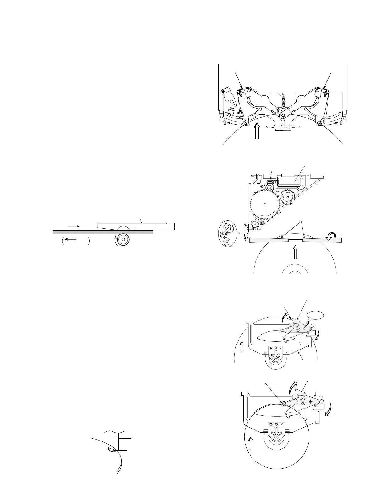
[1] Disc Loading
(1) Turning the loading switch ON
1) When a disc is inserted, the disc arms open to the left and
right and the claw below disc arm (L) sets the loading switch
ON.
2) The above starts the motor rotation.
(2) Loading the disc
1) When the motor starts rotation, the worm gear also starts
to turn as shown in the figure.
2) The rotation force is transmitted to the gear train.
3)When the force is transmitted to the final gear, the rollers
rotate to pull in the disc.
Disc IN
Disc
Disc guide
Switch ON!
Disc arm(L) Disc arm(R)
Disc
Worm gear
Motor
Rubber rollers
Disc OUT
Roller
The disc is pulled in or out when the rollers are pushed against
the disc guide.
[2] Operation of Slider (R)
(1) Activating the trigger arm
1) When the disc is pulled in by the rollers, the disc edge pushes
the trigger arm and rotates it.
2)When the disc is an 8cm disc, it is pulled upwards by the
tapering on the disc guide. The trigger arm is rotated when
the disc pushes the claw (section A) located before the trigger arm.
When the 8cm disc reaches the loading end position, the roller
areas supporting the disc decreases. To pre vent the disc from
dropping in this case, the claw is provided with a projection f or
supporting the disc.
Claw (A)
Side view
Position pushed by the disc
Disc IN
Trigger arm
Clamper chassis
A
Trigger arm
Disc
Projection
8cm Disc
5
X92-4590-0x
Locked
Locked
Center
of rotation
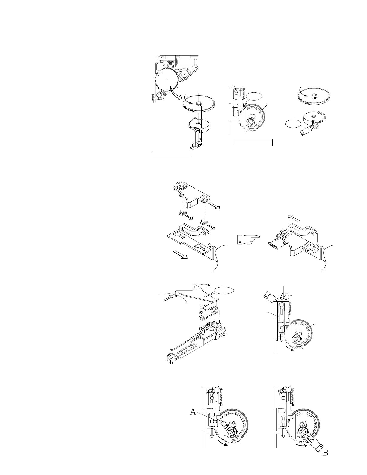
(2) Basic construction (Initial position
of the planetary gear mechanism)
1)Even after the disc has been inserted, the
motor rotated and the gear train also rotated,
slider (R) does not start operation yet.This
is because the planetary gear mechanism
is used and the carrier gear is locked by the
slider mechanism. In this period, the planetary gear is in the loose condition.
2) When the sun gear is rotating and the carrier gear is locked, the planetary gear is running idle.
OPERATION DESCRIPTION
Slider (R)
Sun gear
Carrier gear's rib
Carrier
gear
Planetary gear
Loose condition
Planetary gear
Loose condition
(3) Basic construction (Construction
of the trigger slider and slider (R))
The trigger slider is assembled with slider (R)
and pushed in the direction of the arrow by
the force of a spring.
(4) Operation of slider (R)
1) Activating the trigger slider
When the trigger arm is rotated by the pressure of the disc, the trigger arm pushes the
trigger slider.
2) Rotating (engaging) the planetar y gear
When the trigger slider is moved, it pushes
down the wall (section A) of the carrier gear .
Slider (R)
Tigger arm
Disc
Trigger slider
Trigger slider
Trigger slider
Spring
Trigger arm
Gear teeth
on the traverse
chassis
Carrier gear
(Initial rotation of the carrier gear)
This causes the planetary gear, which is attached on a pin
of the carrier gear, to move according to the rotation of the
carrier gear. When the planetary gear is meshed with a gear
tooth (section B) of the traverse chassis , the planetary gear
starts rotation.
The rotation of the planetary gears causes the carrier gear
to rotate.
6
 Loading...