Kenwood X-92-4570-0x Service Manual
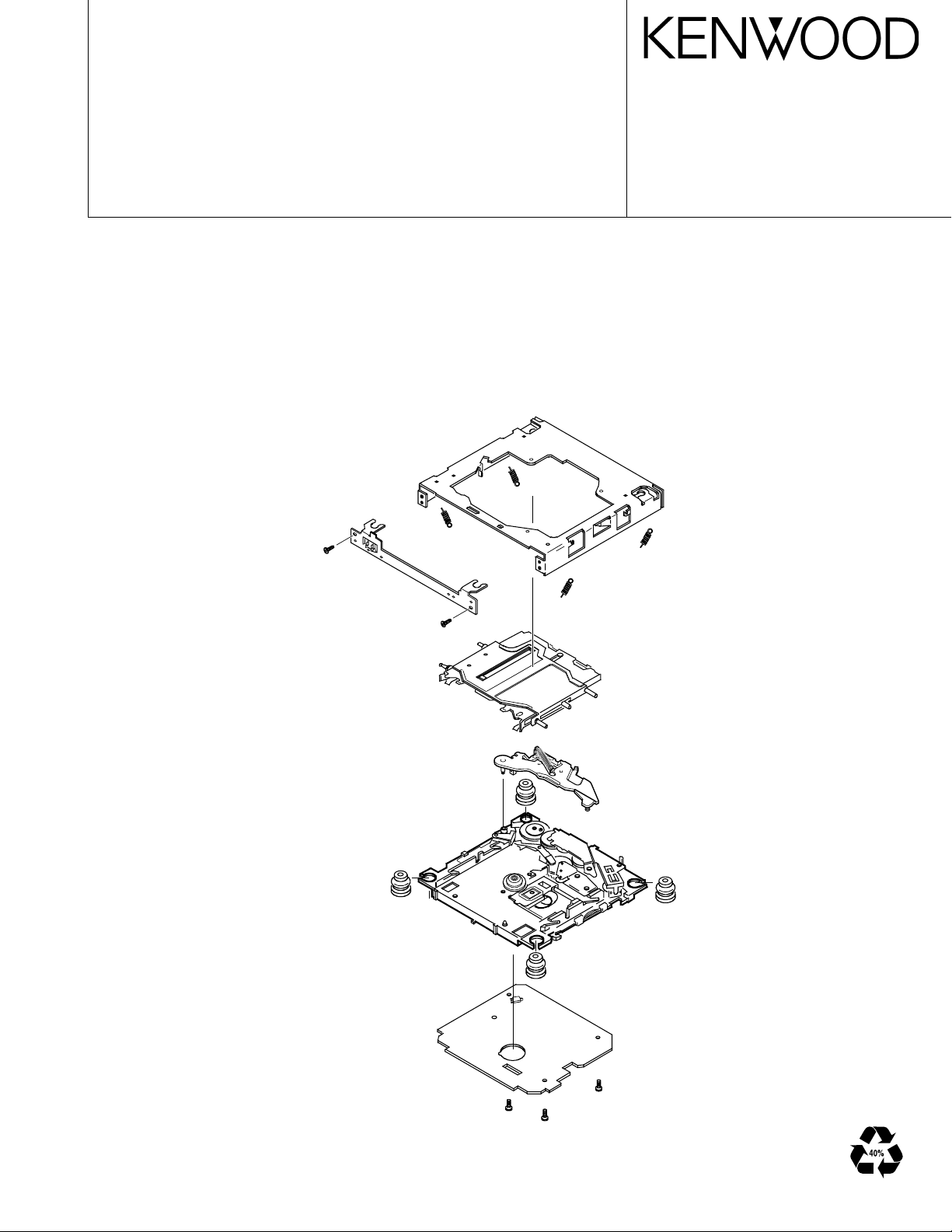
MD MECHANISM ASSY
DESCRIPTION MECHANISM
CONSTRUCTION OF MAJOR PARTS
X92-4110-00 (MDS-3100W)
X92-4110-01 (MDS-3101W)
X92-4570-00 (MDS-3200W)
X92-4570-01 (MDS-3201W)
MP START : Nov. 2001
Outer chassis
Front chassis
Upper chassis assy
Mecha. PCB
Travers chassis assy
Loading arm assy
Air damper x4
Suspension spring x4
X92-4110-0x
X92-4570-0x
SERVICE MANUAL
© 2002-3 PRINTED IN JAPAN
B51-7887-00 (N) 517
2
RF AMP
RF AGC & EQ
IC1
BPF P-P
PEAK &
BOTTOM
ABCD AMP
IV AMP
IV AMP
CVB
AMP
TEMP
VICCONV
ERROR AMP
FOCUS
AT
AMP
BPF
TRACKING
ERROR AMP
SERIAL
PARALLEL
DECODER
BALANCE
E-F
FILTER
PLL
DECODER
ACIRC
EFM
MEMORY
RESISTANT
SHOCK
CONTROLLER
DYNAMIC RAM
ATRAC/ATRAC3
DECODER
DIGITAL
FILTER
CONVERTER
D/A
POST FILTER
CONTROL
MONITOR
ANALOG
MUX
ADIP
DEMODULATOR
DECODER
SPINDLE
SERVO
GENERATOR
PWM
APC
DSP
SERVO
CONVERTER
A/D
CLOCK
GENERATOR
AUTO
SEQUENCER
I/F
CPU
PROCESSOR
SUBCODE
IC7
MECHA MI-COM
CH2
DRIVER
CH1
DRIVER
DRIVER
CH4
DRIVER
CH3
VREF
DRIVER
CH5
IC5
LOE/LIM-SW
LOS/EJE-SW
ATRAC/ATRAC3 DECODER
DET.
REFLECT
APC
CB
DA
F
E
JI
DETECTOR
TRACKING
COIL
FOCUS
COIL
M
LOADING/EJECT/SLED MOTOR
SPINDLE MOTOR
M
THERMISTER
IC9
256
SW+5V
EFM/ACIRC DECODER
SHOCK PROOF MEMORY CONTROLLER
DIGITAL SERVO PROCESSOR
DIGITAL SIGNAL PROCESSOR
1M-WORD 4BIT DYNAMIC RAM
DIGITAL FILTER. D/A CONVERTER
IC2
FOCUS/TRACKING COIL DRIVER
SPINDLE/SLED MOTOR DRIVER
IC4
LOADING/EJECT MOTOR DRIVER
REG.
A3.3V
IC6
A. 8V SW
8BIT
Q8
IC11
IC10
2.5V
REG.
IC3
AUDIO I/F
DIGITAL
Q1,2
5ch BTL
DRIVER
Q4
RF AMP
Q3
DSP
LPF
IC8
Q7
Q5,6,9
1
2
4
5
6
7
8
9
3
15
14
I
J
A
B
C
D
E
F
11
12
22
23
25
41
42
19
APC
APCREF
EQADJ
3TADJ
WBLADJ
FZC
RF
AUX1
AUX2
PEAK
BOTTOM
ABCD
FE
VC
SWDT
SCLK
XLAT
FOCONT
114
113
848577
76
112
111
SPFD
SPRD
FFDR
FRDR
TFDR
TRDR
SFDR
SRDR
25
28
5
15
21
20
MNT0
MNT1
MNT2
MNT3
XINT
SQSY
SENS
SRDT
SCLK
SWDT
XLAT
XRST
44
45
46
62
18
20
19
17
16
FZC
XINT
SQSY
SENS
SRDT
SCLK
SWDT
XLAT
XRST
12
56
231115
1314433659
60
LDON
SDMUTE
LIMIT SW
P-ON
AMUTE
MSDA
MSCL
MSTOP
MRST
TYPE 1
TYPE 2
33
7
8
HOT
ESDA
ESCL
20
19
17
16
30
29
23
22
26
25
24
TRK+
TRK-
FCS+
FCS-
LOAD/SLED+
EJECT/SLED-
SPDL+
SPDLVC
VREF0
VCC2
VCC1
10
11
12
13
7
6
8
9
28
27
3
14
TFDR
TRDR
FFDR
FRDR
LOAD/SFDR
EJECT/SRDR
SPFD
SPRD
REG IN
REG OUT
ENREG
1
11
9
14
13
20
19
15
18
5
6
2
21
7
8
DOUT
L-CH
R-CH
MRST
MSTOP
MSCL (IIC BUS)
MSDA
AMUTE
BU5V
S5V
S5V
LOE/LIM-SW
LOS/EJE-SW
LOAD
EJECT
36
30
29
31
34
35
37
33
38
474648
40
10
28
26
32
17
18
20
27
16
41
40
MORF RFO
AUX 1
FOCONT
XSTBY
ADFG
22.579MHz
6
7
8
35
16
14
13
10
9
11
104
105
106
107
102
84
93
80
81
82
83
67
73
72
71
70
85
92
91
5
11
13
3
1122
10
6
4
8.388MHz
MUTE 1
MUTE 2
1
2
MUTE 3
36
CH1,2
CH3
CH4
21
67
JITTER
RECORD IN
VC
TE
SE
VC
VC
VC
VC
PD
LD
STBY
TO CH5 OP
S+B
SW+5V
S5V
+3.3V
6
5
BU+5V
1.2Vrms
1kHz 0dB
SW+5V
TO SERVO DRIVER
BU+5V
ILCC
LDON
AUDIO +B
DAVDD
SW+5V
A8V
12
34
+2.5V
MOTOR ASSY
DPU1
OPTICAL PICKUP BLOCK
MOTOR BLOCK
MD UNIT
BUFFER
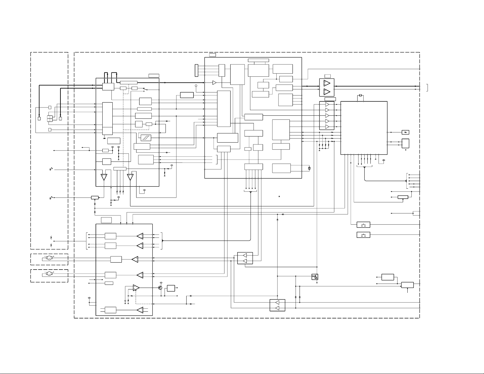
X92-4110-0x/4570-0x
BLOCK DIAGRAM

X92-4110-0x/4570-0x
COMPONENT DESCRIPTION
●MD UNIT(X33-3160/3180-00)
Ref.No.
IC10 TC7WH126FU 3-State buffer
IC11 TC7WH126FU 3-State buffer
Component name Application/Function Operation/Condition/Compatibility
RF amplifier(pits and groove selector type, AGC, EQ), Gain selector
type I-V amplifier, Amplification of the light intensity signal output,
IC1 CXA2523AR RF amplifier for MD Peak hold output, Bottom hold output, FE output, TE output, SE
output, ADIP binary output, VREF output, APC PD amplifier and
FZC formation comparator.
EFM decoding, EFM digital PLL, ACIRC decoding, auto link
IC2 CXD2667R Digital signal processor for MD
IC3 S-817A25ANB +2.5V AVR Power supply for IC2 internal logic circuits.
IC4 LA6572 5 Ch BTL driver
IC5 NJM4580M1 Low pass filter 2nd low pass filter for audio signals.
IC6 LP2982-3.3 A.3.3V AVR Power supply for DAC and LPF operational reference voltage.
IC7 TC74HCT7007AF Buffer Buffer and logic level conversion from IC1,2 to IC8.
780076YGK-R11
IC8
(X33-3160-00)
780076YGK-R14
IC8
(X33-3180-00) Adapted to MD Group.
IC9 W05-0906-00 EEPROM Servo coefficients and servo adjustment data backup memory
2SA1362(Y) or
Q1
2SB1295
DTA114EUA or
Q2
KRA302 or UN5111 turned off.
Q3 2SC4116(Y) Disc refrection detect SW On when focusing point is passed during upward search.
Q4 MCH6101 D.3.3V AVR driver
Q5 DTA143XUA
DTC143EUA or A.8V SW
Q6
KRC401
KTA2014(Y,GR) or
Q7 2SA1576A or SW5V SW
DTC143EUA or
Q8
KRC401 IC10's outputs is Hi-Z operation.
DTC143EUA or
Q9
KRC401 A.+8V is supplying to A.3.3V AVR and low pass filter circuit.
Mecha.MI-COM. Servo control, memory control, system control and interfacing.
Mecha.MI-COM.
APC(Auto Power Control) LD power control
LD SW
2SB1218A
IC10 OUTPUT Hi-Z SW
A.8V SW
processing, ADIP decoding, Digital servos(focusing, tracking, sled,
spindle CLV), ATRAC/ATRAC3 decoding, 1 bit D/A converter,
Analogue post filter and 4M(1Mx4) DRAM built in.
Focusing coil, tracking coil, spindle motor and sled motor driver, disc
loading and eject operation.
Servo control, memory control, system control and interfacing.
When 1, 7 pin goes Hi, Sled servo operation is selected.
When 1, 7 pin goes Lo, IC10's outputs is Hi-Z operation.
When 1, 7 pin goes Hi, Loading/Eject operation is selected.
When 1, 7 pin goes Lo, IC11's outputs is Hi-Z operation.
When Laser OFF mode is selected, Q2's base goes Lo, and Q1 is
When Loading/Eject operation or MD source is selected, Q4's output
is supplying D.3.3V to IC1-3, IC10 and IC11.
When SW5V SW is turned on, Q5 and Q6 are turned on, and A.+8V
is supplying to A.3.3V AVR and low pass filter circuit.
When MD source is selected, P-ON output goes Lo, and BU5V is
supplying to microprocessor peripheral circuits and A.8V SW.
When Loading/Eject operation is selected, Q8's base goes Hi, and
When Loading/Eject operation is selected, Q9's base goes Hi, and
3

X92-4110-0x/4570-0x
MICROCOMPUTER’S TERMINAL DESCRIPTION
●IC8 (MD UNIT: X33-3160/3180-00)
Pin No.
5,6 NC O Not used (N.C.)
10 VDD0 - Positive power supply connection terminal Connected to BU5V lines.
11 P-ON O Unit internal power supply control output Lo: Power on
12 LDON O Laser APC control output Hi: LD on
13 MSDA I/O
14 MSCL I/O
15 AMUTE O Audio muting output Lo: Audio signal muting
16 XRST O DSP LSI & servo driver reset output Lo: Reset
17 XLAT O Latch output to DSP LSI Latch at fall down edge pulse
18 SRDT I Serial data input from DSP LSI
19 SWDT O Serial data output to DSP LSI
20 SCLK O Shift clock output to DSP LSI
21 FLRxD O Data line for flush ROM writing Not used (N.C.)
22 FLTxD O Clock line for flush ROM writing Not used (N.C.)
23 LOE/LIMSW I
24 VDD1 - Positive power supply connection terminal Connected to BU5V lines.
25 AVSS - Ground connection terminal Connected to GND lines.
26 MECHA SEL I Mechanism destination selection input Not used (Connected to GND line)
27-31 NC I Not used (Connected to GND line)
32 AUX1 I Not used (Connected to GND line)
33 HOT I Temperature detection input Vth On: 3.87V, Vth Off: 3.74V
34 AVREF I AD converter reference voltage input terminal
35 AVCON O AVREF control output
36 MRST I Reset input from the system microprocessor Lo: Reset
37 XT2 - Sub clock resonator connection terminal 2 Not used (N.C.)
38 XT1 I Sub clock resonator connection terminal 1 Not used (Connected to BU5V line)
39 VPP I Flush ROM writing terminal Not used (Pull down to GND line)
40 X2 - Main clock resonator connection terminal 2
41 X1 I Main clock resonator connection terminal 1
42 VSS1 - Ground connection terminal Connected to GND lines.
Pin Name I/O Description Processing Operation
1 DEEM O De-emphasis output (Lo: De-emphasis) Not used (N.C.)
2 CSN O External DAC latch line Not used (N.C.)
3 CCLK O External DAC clock line Not used (N.C.)
4 CDTI O External DAC data line Not used (N.C.)
7 ESDA I/O EEPROM serial data line
8 ESCL I/O EEPROM serial clock line
9 VSS0 - Ground connection terminal Connected to GND lines.
Serial data line with the system microprocessor (I2C BUS)
Serial clock line with the system microprocessor (I2C BUS)
Pickup most inner position detect & loading end detect Hi: Loading end
input Hi→Lo: Pickup most inner position detected
Hi: AVREF reference voltage
Lo: AVREF current cut-off (Standby)
4

X92-4110-0x/4570-0x
MICROCOMPUTER’S TERMINAL DESCRIPTION
Pin No.
43 MSTOP I Standby control input from the system microprocessor
44 FZC I FZC interrupt request input
45 XINT I Interrupt request input form DSP LSI Lo: Interrupt status occurrence
46 SQSY I Sub-code Q sink or ADIP sink input
47 FG I FG pulse input (3 hole pulse equivalent) Not used (Connected to GND line)
48 NC O Not used (N.C.)
49 LDEJ IN I
50 LADJ1 I Manual adjustment mode input Hi: Manual adjustment (Focussing Bias
51 TEST3 I Special test mode terminal 3 Not used (Pull down to GND line)
52
53 AGC PASS I Mode switching terminal without automatic adjustment Not used (Pull down to GND line)
54 SE MNT I SE display mode switching input Not used (Pull down to GND line)
55 4M/16M I DRAM size switching input Not used (Connected to GND line)
56 SDMUTE O Sled driver muting control output Hi: Muting on
57 AUDIO INV I DAC output polarity selection input Lo: Polarity non-inverted, Hi: Polar ity inverted
58 M REM O Test mode memory remains output Not used (N.C.)
59 TYPE1 I Destination selection input 1 Not used (Connected to GND line)
60 TYPE2 I Destination selection input 2 Not used (Connected to BU5V line)
61 C1 COUNT I C1 error count display mode switching input Not used (Pull down to GND line)
62 SENS I Internal status input from DSP LSI
63 TEST0 I Test mode terminal 0 Not used (Pull down to GND line)
64 TESTE I Test mode terminal of EEPROM external input Not used (Pull down to GND line)
Pin Name I/O Description Processing Operation
Lo: Standby mode
Lo→Hi: Operation mode (Standby mode released)
Lo→Hi: Media detection (effective only at the time
of the disc detection)
LOAD/EJECT output monitor input form the system When Hi is detected, mechanism microprocessor
microprocessor moves to the play/stop mode.
Lo: Normal operation
adjustment)
IVRTBAL PASS
I Mode switching terminal without automatic adjustment Not used (Pull down to GND line)
5
X92-4110-0x/4570-0x
DESCRIPTION OF MECHANISM OPERATION
1) This mechanism permits the re-loading of a cartridge after
it has been ejected.
2) A cartridge cannot be inserted during power-off due to builtin automatic push-out cartridge (This is for preventing the
breakage of the mechanism).
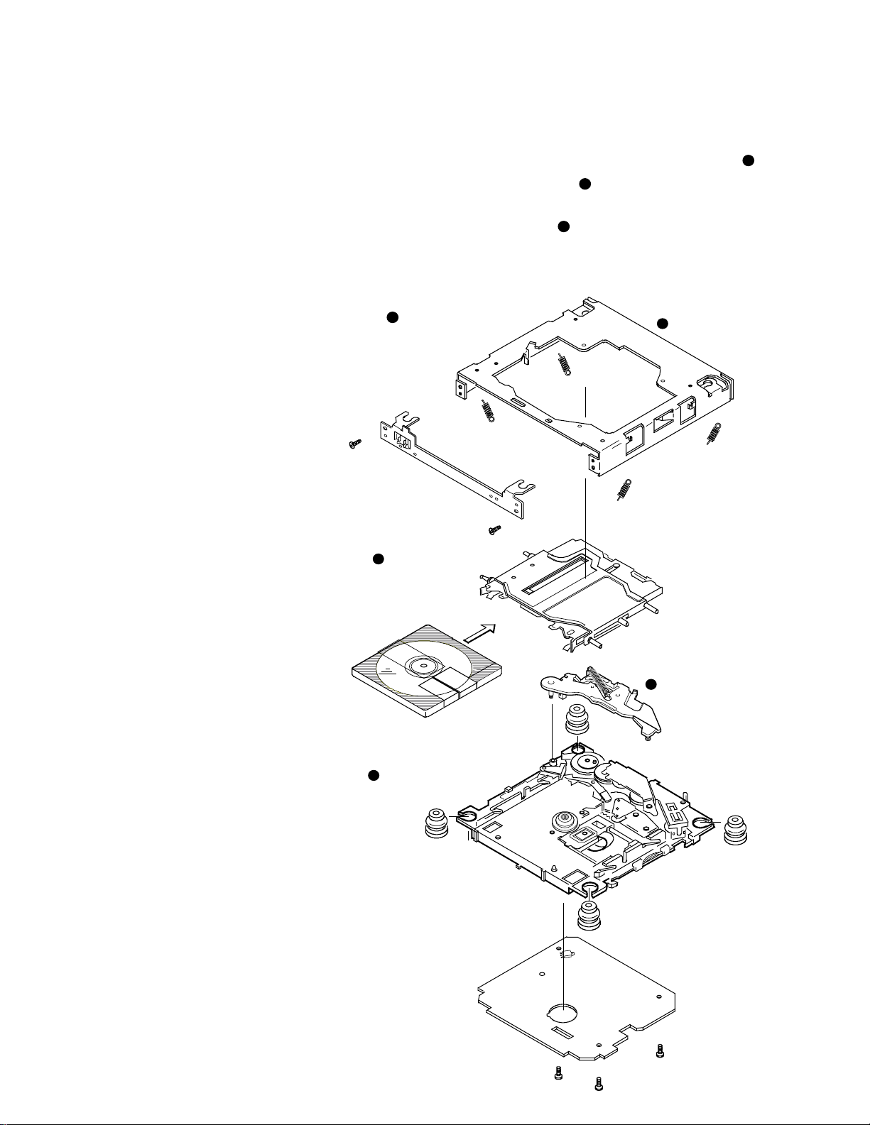
1. Configuration of main components
This mechanism consists of main components as shown
in the figure below.
The main purpose of the traverse chassis assembly (
1
is to hold a cartridge and read its signals form it.
The main purpose of upper chassis assembly (
loading arm assembly (
out a cartridge.
The outer case (
assembly and limiting the positions of the mechanism compo-
nents.
In addition, there is a mechanism PCB.
)
) is to mechanically pull in and push
3
) is for supporting the traverse chassis
4
4
Outer case
2
) and
2
Upper chassis assembly
Cartridge
Traverse chassis assembly
1
Mechanism PCB
Turntable
Loading arm assembly
3
Optical pickup
Air damper x 4
6
X92-4110-0x/4570-0x
6
DESCRIPTION OF MECHANISM OPERATION
2. Operational explanation
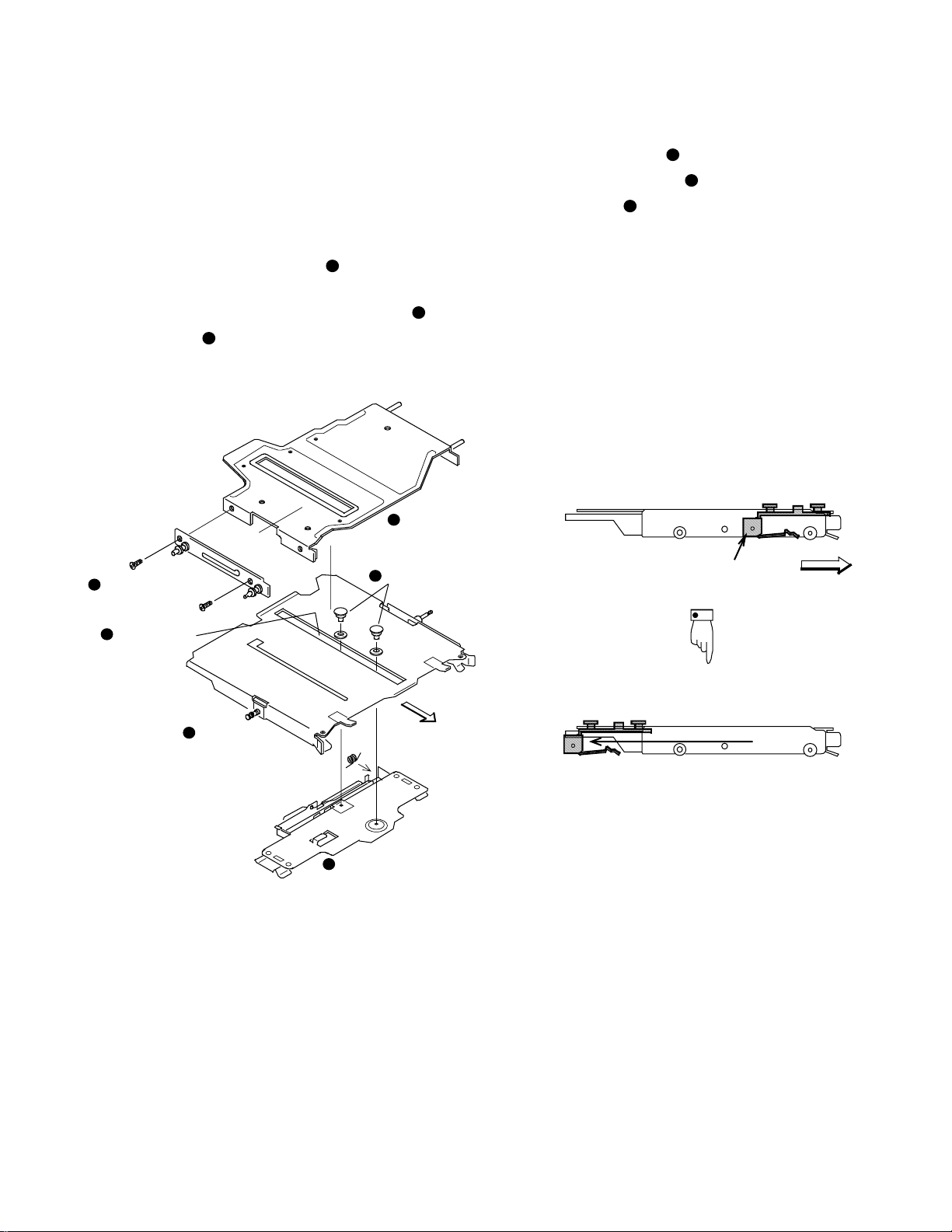
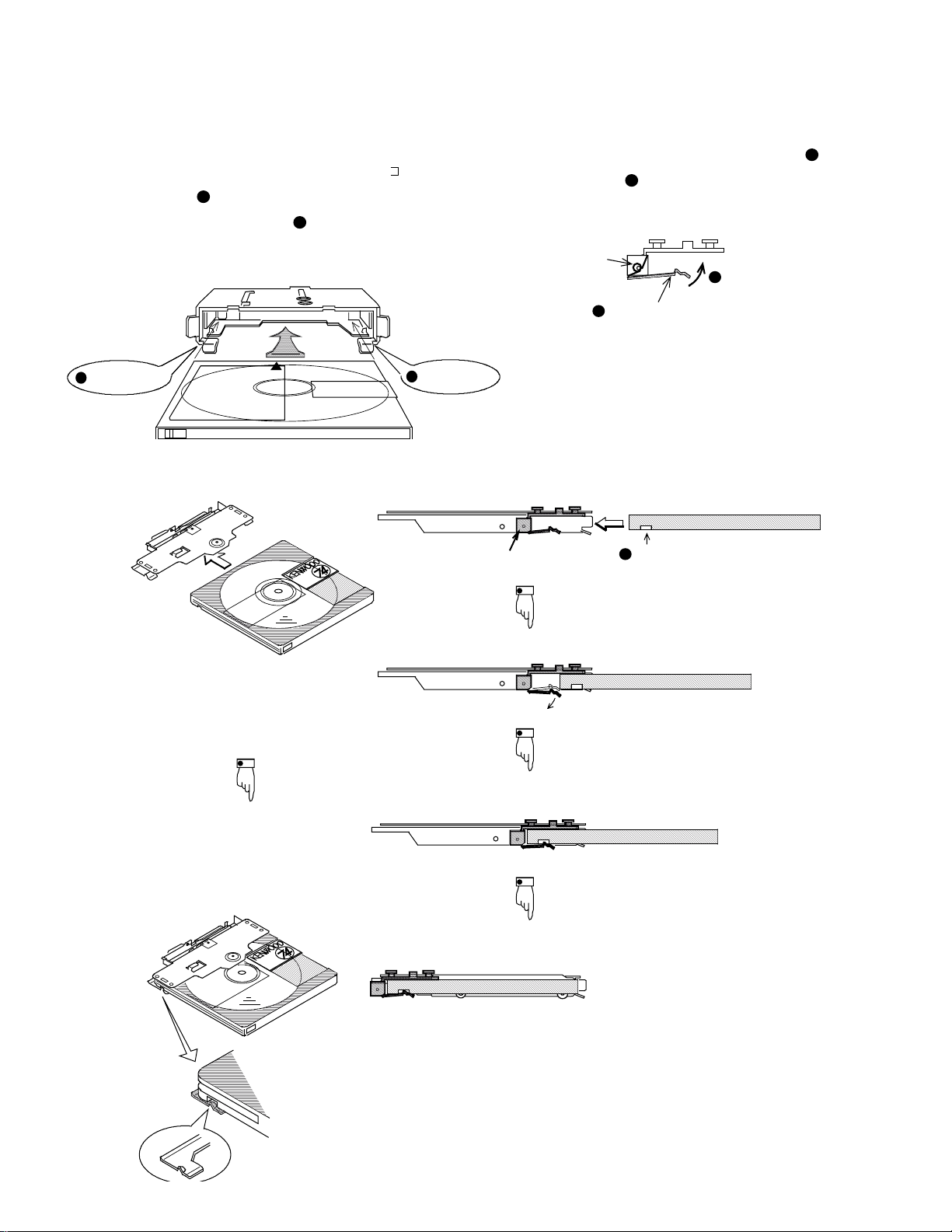
[1] Loading of cartridge
(1) Construction of upper chassis
The upper chassis assembly consists of the carrier f or holding a cartridge and pulling in it up to the position when loading
is to be completed, the carrier base (
moves up and down to playback after opening the shutter of
the cartridge, and the assembly of the UD PLATE (
the UD PLATE L (
rier base.
3
UD PLATE L
) respectively for pushing down the car-
3
) that mechanically
1
2
UD PLATE
2
4
Caulking pins
) and
The carrier assembly (
rier base with caulking pins (
elliptical opening (
) of the carrier base.
5
[Left side view]
Initial position
) is caulking-secured to the car-
) and operates along the long
4
Carrier assembly
Front side
5
Long elliptical
opening
Carrier base
1
6
Carrier assembly
Operation completed position
Front side
(Sliding operation)
7
X92-4110-0x/4570-0x
DESCRIPTION OF MECHANISM OPERATION
(2) Insertion of cartridge
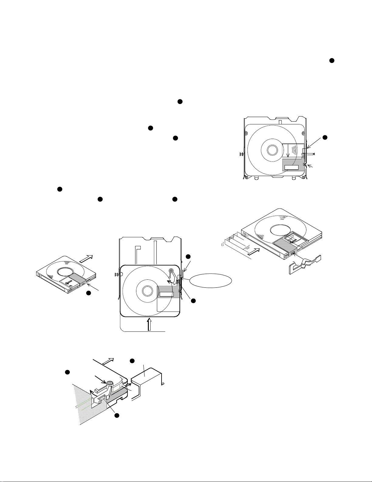
When a cartridge is made to be passed into the “ ”-char-
acter-shaped inlet (
pushed, the hole of the cartridge (
protrusion for holding the cartridge in the carrier assembly to
hold the cartridge.
1
Inlet of cartridge
) of the carrier base and is moreover
1
) is engaged with the
2
Carrier base
1
Inlet of cartridge
[Flow up to insertion of cartridge]
The sub-chassis under the carrier assembly (
been forced upward (
Spring
3
Initial position
Carrier assembly
) by the force of the spring.
4
4
Pushing force
Sub-chassis (bottom side)
Hole
2
Disc
3
) have
Side A
The bottom portion of a cartridge pushes and opens the sub-chassis.
Condition in which a cartridge is held
Cartridge loading completed position
8
X92-4110-0x/4570-0x
Plate spring
Shutter lock portion
Cartridge
Shutter opens
Fixture
7
Shutter
DESCRIPTION OF MECHANISM OPERATION
(3) Opening/closing construction of disc shutter
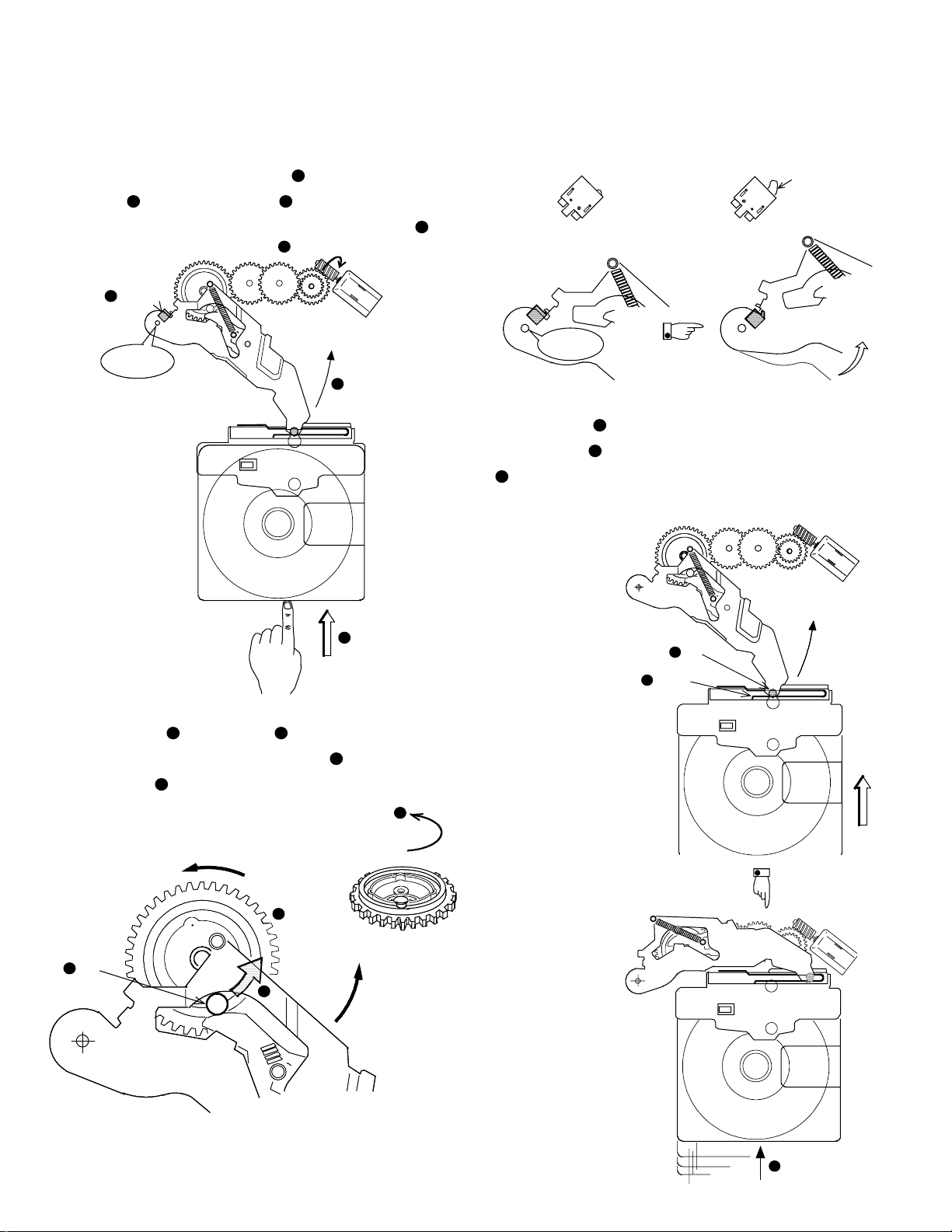
A MD (mini-disc) is entirely covered by a plastic case in
order to protect the disc. The disc is not usually touched directly but the disc is exposed to receiv e the laser beam during
recording and playback.
For this reason, a cartridge is provided with a shutter(
1
and when the shutter is opened to record and playback, a part
of the disc can be exposed.
The shutter is locked by the shutter lock (
This shutter is opened or closed by the plate spring (
).
2
3
) at
the right side within the carrier base.
1) When a cartridge is loaded while being held by the carrier assembly, the car tridge slides into the carrier base .
(See “(2) Insertion of cartridge.”) The claw of the shutter
) then slips when the bending-shaped member of
(
6
the carrier base (
) pushes the shutter lock (2) of
4
the cartridge.
Carrier base assembly
2) Next, the plate spring within the carrier base (
7
) is in-
serted into the window of the shutter and the shutter is
held by it, and the shutter is then opened when only the
cartr idge moves. (The bending-shaped member stops
against the shutter, thereby functioning as a stopper and
),
thereafter the shutter is opened.)
Cartridge
Direction of insertion
Disc
2
Shutter lock
1
Shutter
6
Shutter
Cartridge
4
Bending-shaped member
Claw of shutter
Shutter
3
Plate spring
Bending-shaped
member
2
Shutter lock
9
X92-4110-0x/4570-0x
Before a cartrigde is inserted
(Position in which the switch is off)
After a cartridge is inserted
(Position in which the switch is on)
Actuator
Center of
rotation
DESCRIPTION OF MECHANISM OPERATION
(4) Rotation of loading motor
When a cartr idge is inserted (
pushed (
), so that the switch (3) within the mechanism
2
PCB is turned on, and the loading motor starts to rotate (
3
Switch
Center of
rotation
Loading arm
), the loading arm is
1
Loading motor
4
2
).
4
(6) Loading a car tridge
Since the pin (
with the spring (
(
) when the carrier slides along with the rotational opera-
11
) at the end of the loading arm is coupled
9
) within the carrier, a cartridge is pulled in
10
tion of the loading arm.
(5) Operation of loading arm
The cam gear (
ing arm. This pin pulls up the loading arm (
gear rotates (
7
[Start of pulling in]
Pin
6
Cartridge
1
) has the pin (6) engaged with the load-
5
) when the cam
8
).
7
Cam gear
5
8
[Start of pulling in]
[Completion of pulling in]
10
9
Spring
Pin
Carrier
10
Loading arm
11
 Loading...