

VHF P25 TRANSCEIVER
TK-5210(G
SERVICE MANUAL
Knob (Selector)
(K29-9323-03)
Knob (Volume)
(K29-9322-03)
)
© 2010-7 PRINTED IN JA PAN
B51-8910-10 (N)
As for the hardware of this transceiver, version 3 is used.
The programming software must use KPG-95DG.
TK-5210(G) K TK-5210(G) K2, K7 TK-5210(G) K3
Knob (Selector)
(K29-9323-03)
Helical Antenna
(KRA-22: Option)
Knob (Volume)
(K29-9322-03)
Key top
(EMG)
(K29-9319-03)
Knob (Selector)
(K29-9323-03)
Helical Antenna
(KRA-22: Option)
Knob (Volume)
(K29-9322-03)
Key top
(EMG)
(K29-9319-03)
Helical Antenna
(KRA-22: Option)
Key top
(EMG)
(K29-9319-03)
Knob (PTT)
(K29-9328-02)
Main cabinet
(A02-3875-01)
Knob (PTT)
(K29-9328-02)
Main cabinet
(4key)
(A02-3877-11)
Does not come with antenna. Antenna is available as an option.
CONTENTS
GENERAL .............................................................................2
SYSTEM SET-UP .................................................................3
REALIGNMENT ...................................................................4
INSTALLATION ..................................................................11
DISASSEMBLY FOR REPAIR ............................................12
CIRCUIT DESCRIPTION ..................................................18
COMPONENTS DESCRIPTION .........................................26
PARTS LIST .......................................................................28
EXPLODED VIEW ..............................................................40
PACKING ............................................................................42
TROUBLE SHOOTING ......................................................43
ADJUSTMENT .................................................................45
TERMINAL FUNCTION ....................................................66
Knob (PTT)
(K29-9328-02)
Key top
(4key)
(K29-9320-03)
Main cabinet
(DTMF)
(A02-3879-11)
PC BOARD
CONTROL UNIT (X53-4390-XX) .................................74
TX-RX UNIT (X57-7650-10) .........................................78
INTERCONNECTION DIAGRAM ......................................82
SCHEMATIC DIAGRAM ...................................................84
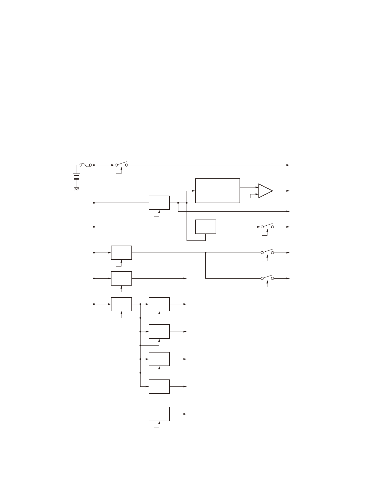
BLOCK DIAGRAM ............................................................96
LEVEL DIAGRAM ...........................................................100
OPTIONAL ACCESSORIES
KNB-32N (Ni-MH Battery Pack) ...............................101
KNB-33L (Li-ion Battery Pack)..................................101
KNB-54N (Ni-MH Battery Pack) ...............................101
KSC-32 (Rapid Charger) ............................................101
KBP-6 (Battery Case) ................................................101
SPECIFICATIONS ..........................................BACK COVER
Key top
(DTMF)
(K29-9321-13)
This product complies with the RoHS directive for the European market.
This product uses Lead Free solder.

TK-5210(G
)
Document Copyrights
Copyright 2010 by Kenwood Corporation. All rights re-
served.
No part of this manual may be reproduced, translated,
distributed, or transmitted in any form or by any means,
electronic, mechanical, photocopying, recording, or otherwise, for any purpose without the prior written permission
of Kenwood.
Disclaimer
While every precaution has been taken in the preparation
of this manual, Kenwood assumes no responsibility for errors or omissions. Neither is any liability assumed for damages resulting from the use of the information contained
herein. Kenwood reserves the right to make changes to any
products herein at any time for improvement purposes.
GENERAL
Firmware Copyrights
The title to and ownership of copyrights for firmware
embedded in Kenwood product memories are reserved for
Kenwood Corporation. Any modifying, reverse engineering, copy, reproducing or disclosing on an Internet website
of the firmware is strictly prohibited without prior written
consent of Kenwood Corporation. Furthermore, any reselling, assigning or transferring of the fi rmware is also strictly
prohibited without embedding the firmware in Kenwood
product memories.
Transceivers containing AMBE+2™ Vocoder:
The AMBE+2™ voice coding technology is embedded
in the fi rmware under the license of Digital Voice Systems,
Inc.
INTRODUCTION
SCOPE OF THIS MANUAL
This manual is intended for use by experienced technicians familiar with similar types of commercial grade communications equipment. It contains all required service
information for the equipment and is current as of the publication date. Changes which may occur after publication
are covered by either Service Bulletins or Manual Revisions.
These are issued as required.
ORDERING REPLACEMENT PARTS
When ordering replacement parts or equipment information, the full part identifi cation number should be included.
This applies to all parts: components, kits, or chassis. If the
part number is not known, include the chassis or kit number
of which it is a part, and a suffi cient description of the required component for proper identifi cation.
Model & Destination
(Market code)
K
TK-5210G
K2 –
K3 – –
K7 –
TX-RX Unit
X57-7650-10
Control Unit X53-4390-XX
0-10 0-11 0-12
✓
––
✓
✓
PERSONAL SAFETY
The following precautions are recommended for personal
safety:
• DO NOT transmit until all RF connectors are verifi ed secure and any open connectors are properly terminated.
• SHUT OFF and DO NOT operate this equipment near
electrical blasting caps or in an explosive atmosphere.
• This equipment should be serviced by a qualifi ed technician only.
SERVICE
This transceiver is designed for easy servicing. Refer to
the schematic diagrams, printed circuit board views, and
alignment procedures contained within.
NOTE
There are two types of FPU for this series. You must use
KPG-95DG version 6.10 or later for transceiver. You can not
use KPG-95D for this transceiver.
Frequency
range
–
136~174MHz
✓ ✓✓✓
–
Remarks LCD 4-key
–––
1st IF: 49.95MHz
LOC: 50.4MHz
✓✓
✓✓
DTMF
keypad
–
–
2
SYSTEM SET-UP
TK-5210(G
)
Merchandise received
License and frequency allocated by FCC
Choose the type of transceiver
Transceiver programming
Are you using the optional antenna?
NO
Are you using the speaker microphone?
NO
Are you using the voice guide & storage unit?
YES
YES
YES
Type
TK-5210G K
TK-5210G K2
TK-5210G K3
TK-5210G K7
A personal computer , programming interface (KPG-36/36A), USB adapter (KCT-53U),
and programming software (KPG-95DG) are required for programming.
(The frequency, and signaling data are programmed for the transceiver.)
KRA-22 or KRA-26
Helical antenna
KMC-25, KMC-41
Speaker microphone
KMC-38GPS
GPS speaker microphone
Frequency range (MHz)
TX/RX 136~174
TX/RX 136~174
TX/RX 136~174
TX/RX 136~174
(Option)
or
(Option)
VGS-1 See page 11.
(Option)NO
RF power
5W
5W
5W
5W
LCD
No
Yes
Yes
Yes
4-key
No
Yes
Yes
Yes
DTMF keypad
No
No
Yes
No
CH
1024
1024
1024
128
Delivery
3
TK-5210(G
)
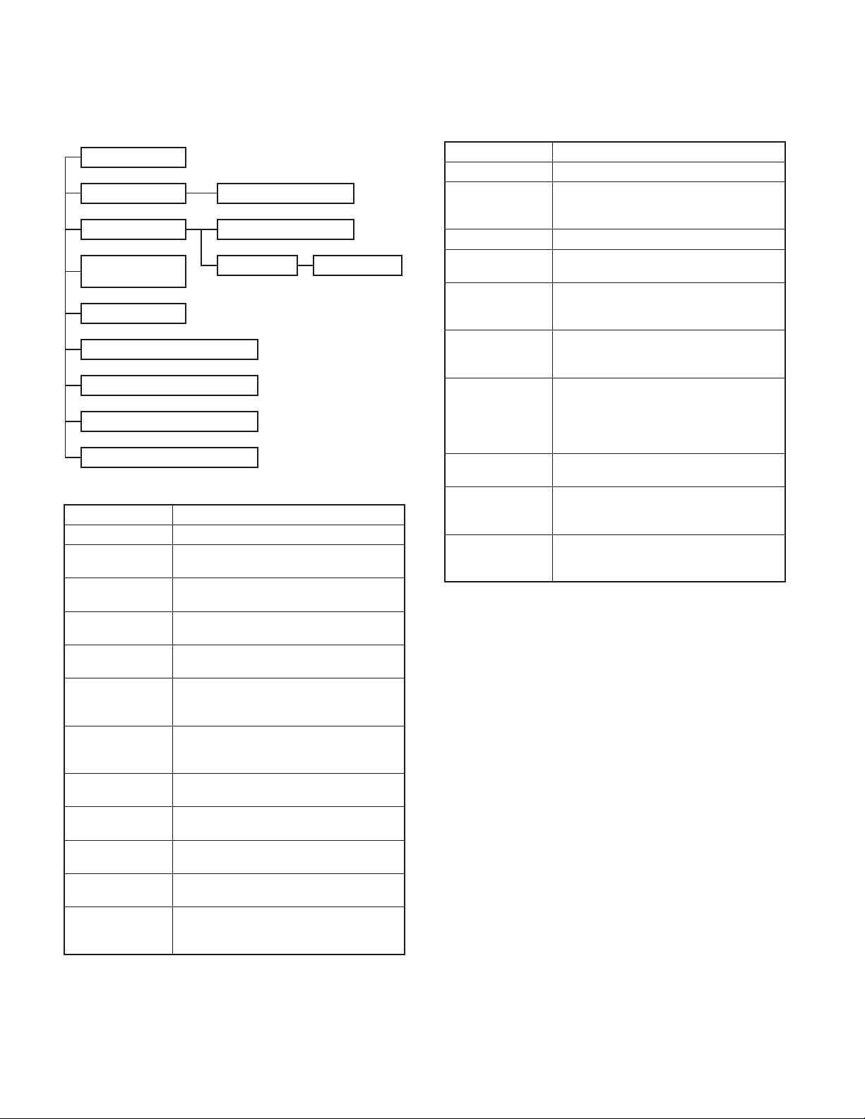
REALIGNMENT
1. Modes
User mode
Panel test mode *1 Panel tuning mode *1
PC mode
Firmware
programming mode
Clone mode *1
Self programming mode *1
Firmware version information *1
Clock adjustment mode *1
Transceiver information mode *1
Mode Function
User mode For normal use.
Panel test mode *1
Panel tuning mode
*1
PC mode
Data programming
mode
PC test mode
Firmware
programming
mode
Clone mode *1
Self programming
mode *1
Firmware version
information *1
Clock adjustment
mode *1
Transceiver
information mode
*1
*1: K2, K3 and K7 models only
Used by the dealer to check the fundamental characteristics.
Used by the dealer to tune the transceiver.
Used for communication between the transceiver and PC.
Used to read and write frequency data and
other features to and from the transceiver.
Used to check the transceiver using the PC.
This feature is included in the FPU.
See panel tuning.
Used when changing the main program of
the fl ash memory.
Used to transfer programming data from
one transceiver to another.
Frequency, signaling and features write to
the transceiver.
Used to confi rm the internal fi rmware version.
Used by the dealer to adjust date and time.
Used to confi rm the transceiver fi rmware
version.
Data programming mode
PC test mode PC tuning mode
2. How to Enter Each Mode
Mode Operation
User mode Power ON
Press and hold the [Side3] and [PTT] keys
Panel test mode *2
PC mode Received commands from PC.
Panel tuning mode
*2
Firmware
programming
mode
Clone mode *2
Self programming
mode *2
Firmware version
information *2
Clock adjustment
mode *2
Transceiver
information mode
*2
*2: K2, K3 and K7 models only
while turning the transceiver power ON and
then release the [PTT] key fi rst.
Press the [Side3] key, in Panel test mode.
Press and hold the [Side3] and [PTT] keys
while turning the transceiver power ON and
then release the [Side3] key fi rst.
Press and hold the [Side2] and [PTT] keys
while turning the transceiver power ON and
then release the [Side2] key fi rst.
Press and hold the [Side2] and [PTT] keys
while turning the transceiver power ON and
then release the [PTT] key fi rst.
And the “INPUT PASSWORD” is displayed,
then release the [Side2] key.
Press and hold the [Side3] key while turning
the transceiver power ON.
Press and hold the [Orange] and [PTT] keys
while turning the transceiver power ON and
then release the [Orange] key fi rst.
Press and hold the [Side1] and [PTT] keys
while turning the transceiver power ON and
then release the [PTT] key fi rst.
3. Panel Test Mode
(K2, K3 and K7 models only)
Setting method refer to ADJUSTMENT.
4.
Panel Tuning Mode
(K2, K3 and K7 models only)
Setting method refer to ADJUSTMENT.
4

REALIGNMENT
TK-5210(G
)
5. PC Mode
5-1. Preface
The transceiver is programmed by using a personal computer, programming interface (KPG-36/36A), USB adapter
(KCT-53U) and programming software (KPG-95DG).
The programming software can be used with a PC. Figure 1 shows the setup of a PC for programming.
PC
KPG-95DG
(ver. 6.10 or later)
PC
D-SUB
(25-pin)
KPG-36
Transceiver
PC
D-SUB
(9-pin)
KPG-36A
Transceiver
Fig. 1
5-2. Connection procedure
1. Connect the transceiver to the computer using the inter-
face cable and USB adapter (When the interface cable is
KPG-36A, the KCT-53U can be used.).
KPG-36 or KPG-36A or
KPG-36A + KCT-53U
Illustration is KPG-36.
PC
USB
KCT-53U
KPG-36A
Transceiver
5-3. KPG-36/KPG-36A description
(PC programming interface cable: Option)
The KPG-36/36A is required to interface the transceiver
to the computer. It has a circuit in its D-sub connector (KPG36: 25-pin, KPG-36A: 9-pin) case that converts the RS-232C
logic level to the TTL level.
The KPG-36/36A connects the universal connector of the
transceiver to the RS-232C serial port of the computer.
5-4. KCT-53U description (USB adapter: Option)
The KCT-53U is a cable which connects the KPG-36A to
a USB port on a computer.
When using the KCT-53U, install the supplied CD-ROM
(with driver software) in the computer. The KCT-53U driver
runs under Windows 2000, XP or Vista (32-bit).
5-5. Programming software KPG-95DG description
The KPG-95DG is the programming software for the
transceiver supplied on a CD-ROM. This software runs under Windows 98, ME, Windows NT4.0, Windows 2000, XP
or Vista (32-bit) on a PC.
The data can be input to or read from the transceiver and
edited on the screen. The programmed or edited data can
be printed out. It is also possible to tune the transceiver.
6. Firmware Programming Mode
6-1. Preface
Flash memory is mounted on the transceiver. This allows the transceiver to be upgraded when new features are
released in the future. (For details on how to obtain the fi rmware, contact Customer Service.)
6-2. Connection procedure
Connect the transceiver to the personal computer using
the interface cable (KPG-36/36A) and USB adapter (KCT-53U:
when the interface cable is KPG-36A, the KCT-53U can be
used.). (Connection is the same as in the PC Mode.)
Note:
• You must install the KCT-53U driver in the computer to
use the USB adapter (KCT-53U).
• When using the USB adapter (KCT-53U) for the fi rst time,
plug the KCT-53U into a USB port on the computer with
the computer power ON.
2. When the POWER switch on, user mode can be entered
immediately. When PC sends command the transceiverenter PC mode, and “PROGRAM” is displayed on the
LCD. When data transmitting from transceiver, the red
LED is lights.
When data receiving to transceiver, the green LED is
lights.
Note:
• The text message are displayed for K2, K3 and K7 models only.
• The data stored in the computer must match the “Model
Name and Market Code” when it is written into the fl ash
memory.
6-3. Programming
1. Start up the fi rmware programming software (Fpro.exe).
2. Set the communications speed (normally, 115200 bps)
and communications port in the confi guration item.
3. Set the fi rmware to be updated by File name item.
4. Press and hold the [Side3] and [PTT] keys while turning
the transceiver power ON and then release the [Side3]
key fi rst. Then, the orange LED on the transceiver lights.
And the “PROGRAM FIRMWARE” is displayed for K2,
K3 and K7 models only.
5. Check the connection between the transceiver and the
personal computer, and make sure that the transceiver is
in the Program mode.
6. Press “write” button in the window. The orange LED
turns off while the firmware is being erased, and the
green LED turns on when the fi rmware data is being received.
7. If writing ends successfully, the checksum is calculated
and a result is displayed.
8. If you want to continue programming other transceivers,
repeat steps 4 to 7.
5
TK-5210(G
)
REALIGNMENT
Note:
• This mode cannot be entered if the Firmware Programming mode is set to Disable in the Programming software.
• The text message are displayed for K2, K3 and K7 models only.
• These transceivers use fi rmware versions G5.10 or later.
When using fi rmware versions earlier than version G5.10
a “Check connection” error message will appear on the
LCD. Firmware versions earlier than version G5.10 will
not write to the transceiver.
6-4. Checksum display
1. If you press the [Side1] switch (top of left side) while
“PROGRAM FIRMWARE” is displayed, the checksum
is calculated, and a result is displayed. If you press the
[Side1] switch again while the checksum is displayed,
“PROGRAM FIRMWARE” is redisplayed.
Note:
• Normally, write in the high-speed mode.
• The text message are displayed for K2, K3 and K7 models only.
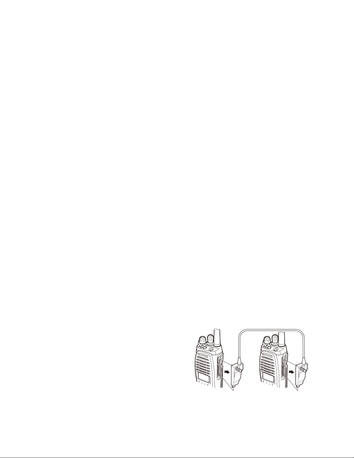
7.
Clone Mode (K2, K3 and K7 models only)
Programming data can be transferred from one trans-
ceiver to another by connecting them via their external universal connectors. The operation is as follows (the transmit
transceiver is the source and the receive transceiver is a
target).
The following data cannot be cloned.
• Tuning data
• Embedded message with password
• Model name data
• ESN (Electronic Serial Number) data
• Network fi le data (P25)
Key guide on the “INPUT PASSWORD” display.
• CNF ([A] key): The password confi rmation
• DEL ([B] key): Delete the least digit from the current
password number (Press and hold to delete all password
numbers)
• SET ([D] key): Determine the least digit of the password
number
3.
• How to enter the password using the keypad (K3
model only);
If the [D] key is pressed while “CLONE LOCK” is dis-
played, the Read authorization password input screen
(INPUT PASSWORD) is displayed.If one of keys 0 to 9
is pressed while “INPUT PASSWORD” is displayed, the
pressed number is displayed on the LCD. Each press of
the key shifts the display in order to the left. When you
enter the password and press the [A] or [*] key, “CLONE
MODE” is displayed if the entered password is correct.
If the password is incorrect, “CLONE LOCK” is redisplayed.
• How to enter the password using the [Side2] and
[Side3] keys (K2, K3 and K7 models);
If the [D] key is pressed while “CLONE LOCK” is dis-
played, the Read authorization password input screen
(INPUT PASSWORD) is displayed. If the [Side2] key or
[Side3] key is pressed while “INPUT PASSWORD” is
displayed, the number (0 to 9) fl ashes on the LCD. When
you press the [D] key, the currently selected number
is determined. If you press the [A] key after entering
the password in this procedure, “CLONE MODE” is
displayed if the entered password is correct. If the password is incorrect, “CLONE LOCK” is redisplayed.
4. Power ON the target transceiver.
5. Connect the cloning cable (part No. E30-3325-05) to the
universal connectors on the source and target.
6. Press the [Side1] or [A] key on the source while the
source displays “CLONE MODE”. The data of the source
is sent to the target. While the target is receiving the
data, “PROGRAM” is displayed. When cloning of data
is completed, the source displays “END”, and the target
automatically operates in the User mode. The target can
then be operated by the same program as the source.
7. The other target can be continuously cloned. When the
[Side1] or [A] key on the source is pressed while the
source displays “END”, the source displays “CLONE
MODE”. Carry out the operation in step 4 to 6.
8. To return to “User mode” on the source transceiver, you
must first turn the transceiver power off and then on
again.
Cloning cable
(E30-3325-05)
1. Press and hold the [Side2] and [PTT] keys while turning
the transceiver power ON and then release the [Side2]
key fi rst. If the Read authorization password is set to the
transceiver, the transceiver displays “CLONE LOCK”. If
the password is not set, the transceiver displays “CLONE
MODE”.
2. When you enter the correct password, and “CLONE
MODE” is displayed, the transceiver can be used as the
cloning source. The following describes how to enter the
password.
6
Fig. 2
Note:
• You can not clone transceivers using hardware version 1.0
or 2.0.
REALIGNMENT
TK-5210(G
)
• Cloning is only possible when transceivers are using
hardware version 3.0.
• You can not clone if the password (overwrite password)
is programmed to the target.
• You can not clone if the checksum in the Network File
area of the source transceiver and the target transceiver
is different.
• ”Model Name and Market Code” must be same to clone
the transceiver. However, it may be unable to clone the
transceiver depending on the enhanced features settings. (Refer to the FPU for the enhanced features details.)
• Under certain conditions, clone mode cannot be activated even if the clone mode of the source transceiver,
using Hardware Version 3.0, is set to enable. Refer to
the FPU for more details.
8. Self Programming Mode
(K2, K3 and K7 models only)
Write mode for frequency data and signaling etc. To be
used ONLY by the authorized service person maintaining
the user's equipment.
The following setup items in the channels programmed
by the FPU can be changed using the “Self-programming”
mode. The addition of new channel and the deletion of
channel that has already been programmed by the FPU cannot be performed using the self-programming mode.
• RX frequency
• TX frequency
• Channel type
• TX mode (When the channel type is selected “MIXED”.)
• Channel spacing (When the channel type is selected
“ANALOG” ro “MIXED”.)
• RX signaling
• TX signaling
• RX NAC
• TX NAC
• Talkgroup list number
Note:
The personality will be also changed when the above-
mentioned items is changed. (Refer to the FPU for the
personality details.)
Key guide on the “INPUT PASSWORD” display.
• CNF ([A] key): The password confi rmation
• DEL ([B] key): Delete the least digit from the current
password number (Press and hold to delete all password
numbers)
• SET ([D] key): Determine the least digit of the password
number
8-1. Enter to the self programming mode
Press and hold the [Side2] and [PTT] keys while turning
the transceiver power ON and then release the [PTT] key
fi rst. Ignoring whether the Read authorization password is
set or not, “INPUT PASSWORD” appears, then release the
[Side2] key.
If the Read authorization password is not set to the
transceiver, “SELF PROG MODE” is displayed on the LCD
when the [A] key is pressed while “INPUT PASSWORD” is
displayed.
If the password is set to the transceiver, “SELF PROG
MODE” is displayed on the LCD when you enter the correct
password while “INPUT PASSWORD” is displayed.
For the password input method, see “7.Clone Mode”
step 3 described on page 6.
Note :
This mode (self programming mode) cannot be set when
it has been disabled with the FPU.
8-2. Data Writing
Before moving to the next Zone/Channel, “KEEP THIS
CHANGE?” appears on the LCD, if you select ”YES”, the
new data is written to memory. IF you select “NO”, the
new data will not be written; the new data will be erased.
• The setup items for self programming mode are as follows.
No. Setup item Display Remarks
Select
1
Zone/Channel
2 RX frequency RX Freq Receive frequency
3 TX frequency TX Freq Transmit frequency
4 Channel type CH Type ANALOG/P25/MIXED
5 TX mode TX Mode ANALOG/P25
6 Channel spacing CH Space
7 RX Signaling RX Sig Receive QT/DQT
8 TX Signaling TX Sig Transmit QT/DQT
9 RX NAC RX NAC
10 TX NAC TX NAC
11 Talkgroup list number TG List No.
ZONE [
ZONE
***
***
] -CH
-CH [
***
***
***
***
***
Zone: 1~100
]
CH: 1~512
25.0kHz/12.5kHz (When the Channel type is selected “ANALOG” or “MIXED”.)
P25 12.5kHz
000~FFF (Hexadecimal) Note: “F7F” cannot be set.
000~FFF (Hexadecimal) Note: “F7E” and “F7F” cannot be set.
1~250
[K7 model only Zone: 1~32, CH: 1~128]
7

TK-5210(G
Key operation
Item
Key
[A] Go to the next item
[B]
[C]
[D]
[Side3] Unused Unused
Keypad
[0]~[9]
(K3 model only)
Zone-
Channel
Zone/Channel
switching
Zone/Channel
down
Zone/Channel
up
Unused Go to the direct enter mode Unused
Frequency
2.5kHz/5kHz/6.25kHz/
)
RX
7.5kHz/1MHz
step switching
1 step down
1 step up
TX
Frequency
ON/OFF
switching
REALIGNMENT
Channel Type TX Mode
Unused
ANALOG/P25/MIXED
switching (Back)
ANALOG/P25/MIXED
switching (Forward)
ANALOG/P25
switching (Back)
ANALOG/P25
switching (Forward)
Unused
Channel
Spacing
Channel spacing
switching (Back)
Channel spacing
switching (Forward)
RX Signaling TX Signaling
QT/DQT(N)/DQT(I)/OFF
switching
Signaling down
Signaling up
1 step/Standard
switching
Go to the direct enter mode
(After selecting signaling type)
Item
Key
[A] Go to the next item
[B] Delete the least digit from the current number (Press and hold to delete all numbers.) Unused
[C] Unused TG List number down
[D] Determine the least digit TG List number up
[Side2] Increment a number in the specifi ed digit Unused
[Side3] Decrement a number in the specifi ed digit Unused
Keypad
(K3 model only)
A: Press [2] with PTT B: Press [5] with PTT C: Press [8] with PTT
D: Press [0] with PTT E: Press [#] with PTT F: Press [*] with PTT
RX NAC TX NAC TG List No.
Add a digit to the current number
How to enter the “A” ~ “F” is follows.
Unused
• Direct enter mode
Item
Key
[A] Return to non-direct enter mode
[B] Unused Change the type of signaling and return to non-direct enter mode
[C] Unused
[D] Delete the least digit from the current number (Press and hold to delete all numbers.)
[Side3] ON/OFF switching at TX Frequency Unused
Keypad
[0]~[9]
Keypad
[*]
Keypad
[#]
RX Frequency TX Frequency RX Signaling RX Signaling
Add a digit to the current number
Return to non-direct enter mode
Delete the least digit from the current number (Press and hold to delete all numbers.)
8
• Self programming mode fl ow chart
REALIGNMENT
TK-5210(G
)
[Side2] + [PTT] + POWER ON Release [PTT]
KEEP THIS CHANGE?
[A] or [D]
[A]
[Channel type] : “P25”
[A] [A]
[TX frequency] : “OFF”
[Channel type] : “ANALOG” “MIXED”
[A]
[TX frequency] : “OFF”
[Channel type] : “ANALOG”
[A]
[TX frequency] : “OFF”
[Channel type] : “MIXED”
Input Password
Read authorization password entry (6 digits)
[A]
Self programming mode
[A]
Zone/Channel
[A]
RX frequency
[A]
TX frequency
[A]
Channel type
[TX frequency] : Other than “OFF”
[Channel type] : “MIXED”
TX mode
[A]
Channel spacing
[A]
[Channel type] : “ANALOG” or “MIXED”
RX signaling
[A]
[TX frequency] : Other than “OFF”
[Channel type] : “ANALOG” or “MIXED”
[TX mode] : “ANALOG”
[Side 3]
Zone selection
OFF
ANALOG
OFF QT
[B]
Channel selection
[C]/[D]
[C]/[D]
[B] [B] [B]
[B]
[B]
[C]/[D]
P25
P25ANALOG
DQT N
[C]/[D]
MIXED
[C]/[D]
12.5kHz25.0kHz
DQT I
[A]
[Channel type] : “ANALOG”
[A]
[TX frequency] : “OFF”
Squelch type : “NAC” *1
or
[TX frequency] : Other than “OFF”
[Channel type] : “MIXED”
[TX mode] : “ANALOG”
Squelch type : “NAC” *1
[A]
Talkgroup ID List Amount : 0
*1 The squelch type can not be set using the self-programming mode.
[A]
[TX frequency] : “OFF”
[Squelch type] : not “NAC”
TX signaling
RX NAC
TX NAC
Talkgroup list number
OFF QT DQT N
[A]
[B]
[Channel type] : “MIXED”
[A]
[TX frequency] : Other than “OFF”
[Channel type] : “P25” or “MIXED”
If [Channel type] is set to “MIXED”, [TX mode] must be set to “P25”.
[A]
[Channel type] : “P25” or “MIXED”
Talkgroup ID List Amount must not be 0.
[A]
[B]
[B]
DQT I
9
TK-5210(G
)
9. Firmware Version Information
(K2, K3 and K7 models only)
Press and hold the [Side3] key while turning the transceiver power ON and then keep pressing and holding the
[Side3] key, the fi rmware version information appears on the
LCD.
10. Clock Adjustment Mode
(K2, K3 and K7 models only)
10-1. Flow chart of operation
[Orange] + [PTT] + Power ON Release [Orange]
REALIGNMENT
YEAR
[A]
MONTH
[A]
DAY
[A]
HOUR
[A]
MINUTE
[A]
[Side2] and [Side3] keys or [C],[D] and [B] keys
[Side2] and [Side3] keys or [C],[D] and [B] keys
[Side2] and [Side3] keys or [C],[D] and [B] keys
[Side2] and [Side3] keys or [C],[D] and [B] keys
[Side2] and [Side3] keys or [C],[D] and [B] keys
Completion
11. Transceiver Information Mode
(K2, K3 and K7 models only)
Use this function to confirm the transceiver firmware
version.
1 Press and hold the [Side1] and [PTT] keys while turning
the transceiver power ON and then release the [PTT] key
fi rst.
2. The transceiver fi rmware version appears on the LCD.
3. To exit the transceiver information mode, turn the trans-
ceiver power OFF.
10
INSTALLATION
TK-5210(G
)
Voice Guide & Storage Unit (VGS-1: Option)
Installing the VGS-1 unit in the transceiver
■
1. Remove the 4 screws from the cover.
2. Remove the cover by inserting the tip of a pair of tweezers into the screw hole of the cover and prying it open.
Fig. 1
5. Insert the VGS-1 connector (CN1) into the connector
(CN501) of the TX-RX PCB.
Cushion
(G13-1995-04)
20X30X1.0mm
VGS-1
VGS-1
CN1
CN501
Fig. 3
6. Reinstall the cover using the 4 screws removed in step 1.
Cushion
(G13-1992-04)
21X21X2.5mm
3. Remove the OPTION PCB from the connector (CN501)
of the TX-RX PCB.
OPTION PCB
CN501
Fig. 2
4. Attach two cushions to the VGS-1 as shown in the fi gure
3.
Note:
Be sure not to cover the VGS-1 connector (CN1) with the
cushion.
Note:
You must setup using the KPG-95DG.
11
TK-5210(G
)
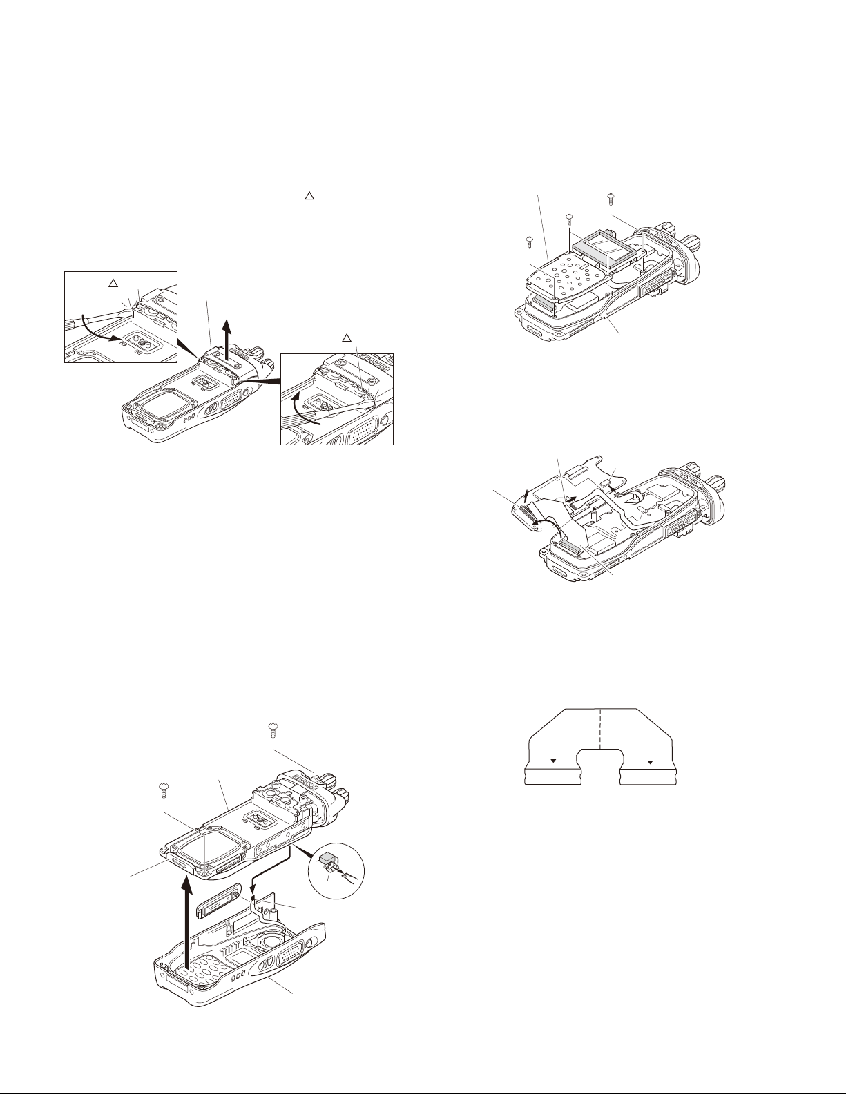
DISASSEMBLY FOR REPAIR
Disassembly Procedure
Removing the front case from the chassis
■
1. Remove the rear panel with a fl at-head screwdriver.
Insert the screwdriver between the rear panel (right side)
and the chassis (the place next to the “
on the chassis), push it in the direction of the arrow q,
and remove the right side of the rear panel. Repeat the
above action for the left side of the rear panel w.
” mark shown
Removing the CONTROL PCB (X53-439) from
■
the chassis
1. Remove the six screws u.
CONTROL PCB
>
>
>
“ ” mark
@
2. Remove the four screws e and universal connector cap
.
r
3. Lift the battery pack release latch on the bottom of the
chassis t and remove the chassis from the front case.
Rear panel
“ ” mark
:
Note:
• Lift the chassis from the front case slowly and carefully.
If the chassis is lifted suddenly, the SP/MIC FPC may be
pulled and the connector may become damaged.
• Handle the main packing with care. It is likely to collect
dust and dirt.
4. Remove the SP/MIC FPC from the CONTROL PCB con-
nector (CN34) y.
Chassis
2. On the reverse side of the CONTROL PCB i, remove
the cord ASSY and each FPC from the connectors (CN40,
CN35, CN38) of the CONTROL PCB.
CN35
CN40
2
Note:
Fold indications are printed on the Cord ASSY and Uni-
versal Connector FPC.
“- - - -” line shows creased line on the bottom.
CN38
Cord ASSY
12
Battery pack
release latch
.
CONT
.
Chassis
Cord ASSY
B
;
=
Front case
CN34
SP/MIC FPC
TX-RX
DISASSEMBLY FOR REPAIR
TK-5210(G
)
Removing the TX-RX PCB (X57-765 A/3) from
■
the chassis
1. Remove the 14 screws o.
2. Remove the universal connector FPC from the TX-RX
PCB connector (CN505) !0.
3. Insert the two tips of a pair of tweezers into the two
holes in the bottom of the shield plate of the TX-RX PCB,
firmly squeeze the tweezers to hold the shield plate,
then remove the TX-RX PCB !1.
4. Remove the coaxial cables from the connector (MAIN
(CN101), UNIV (CN102) of the TX-RX PCB !2.
UNIV
(CN102)
8
TX-RX PCB
8
8
8
8
8
Chassis
8
Universal
connector FPC
MAIN
(CN101)
CN505
Removing the TOP PCB (X57-765 B/3) from the
■
chassis
1. Remove the two screws !9.
2. Lift the TOP PCB and remove the VOL/CH FPC @0 and
CONTROL-TOP FPC @1 from the two connectors (CN902,
CN903) of the TOP PCB.
TOP PCB
CN902
CN903
Precautions for Reassembly
Installing the VOL/CH FPC and CONTROL-TOP
■
FPC on the TOP PCB
1. Remove the volume q and channel switch w from the
chassis.
2. Position the coaxial cable connecting the ANT PCB and
TX-RX PCB as shown in the fi gure below.
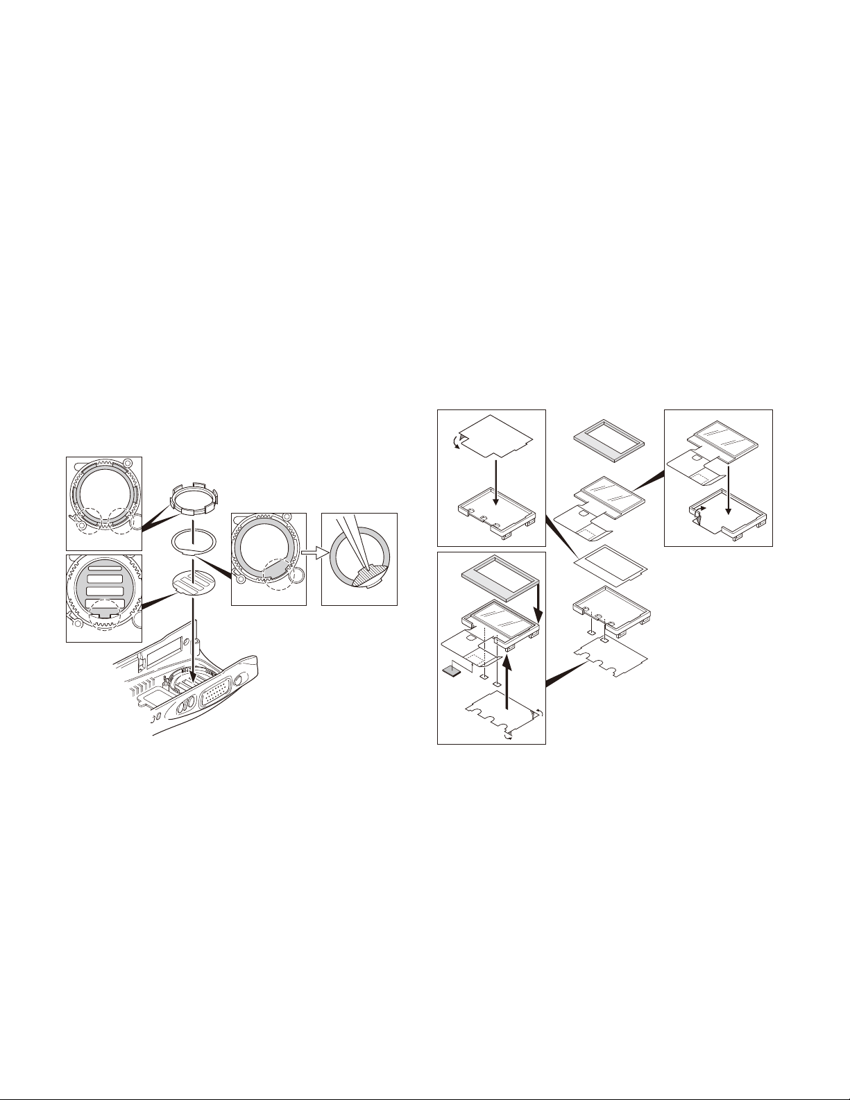
Removing the top panel from the chassis
■
1. Remove the volume knob
2. Remove the concentric switch knob !5.
3. Remove the volume torque-up packing !6 using a pair of
tweezers.
4. Remove the nuts from the volume knob, channel knob
and antenna receptacle.
5. Remove the top panel !7.
and channel knob !4.
!3
Note:
• Before removing the top panel, set the lever switch to
the “●” position (circle painted in white) !8.
• Each of the volume knob, channel knob and antenna receptacle on the top panel has an O-ring. Take care not to
lose them after removing the panel.
Sheet
O-ring
The projection
of the volume
pedestal
:
CONTROL-TOP
FPC
3. Pass the coaxial cable e of the antenna receptacle
through the round hole of the hardware fi xture r, then
insert it into the coaxial connector (MAIN (CN101)) of the
TX-RX PCB.
@
VOL/CH FPC
MAIN
(CN101)
Aline the coaxial cable
connecting the ANT PCB and
TX-RX PCB as shown in the figure.
.
The projection of
the channel
switch pedestal
;
13
TK-5210(G
tab
CONTROL PCB
)
DISASSEMBLY FOR REPAIR
4. Pass the volume, channel switch, VOL/CH FPC and
CONTROL-TOP FPC through hardware fixture holes,
then bring the hardware fixture into contact with the
chassis and fi x it with a screw t.
Note:
The projections of the volume and channel switch ped-
estals must protrude from the square holes of the hardware fi xture.
5. Fix the antenna receptacle with the two screws y.
6. Fix the hardware fi xture with a screw u.
=
>
B
7. Insert the VOL/CH FPC i and the CONTROL-TOP FPC
. into the connectors (CN902, CN903) of the TOP PCB.
o
8. Fix the TOP PCB with a screw !0.
9. Fix the TOP PCB with a screw !1.
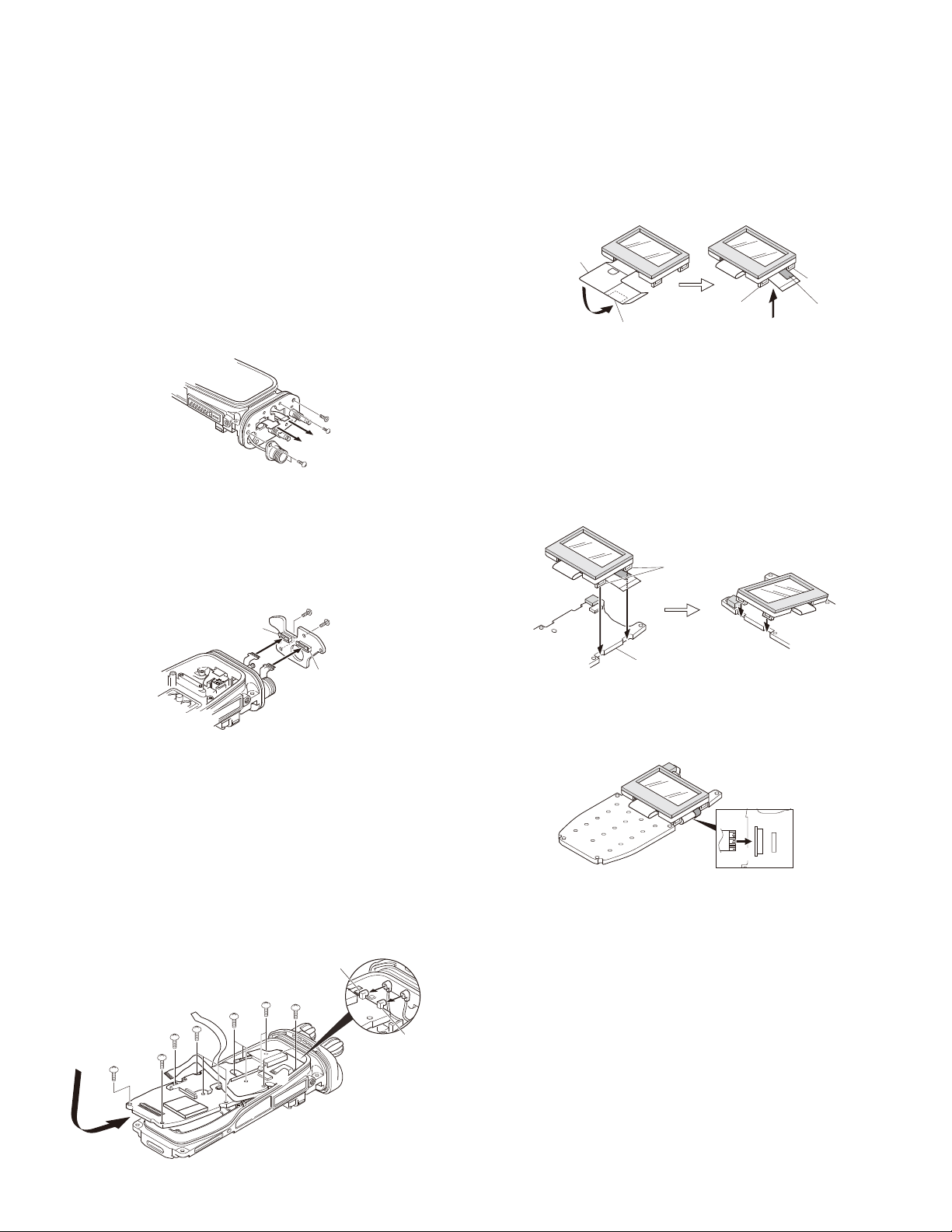
LCD ASSY Installation Procedure
■
1. Fold the LCD ASSY FPC to the back of the holder q so
that the FPC is between the two tabs on the right side of
the holder w.
LCD ASSY FPC
tab
:
Sheet
2. Fit the two tabs on the right side of the holder e and the
two tabs on the left side of the holder r into the CONTROL PCB.
tab
@
Sheet
Note:
Take care that the FPC is not caught when fi tting the two
tabs on the right side of the holder.
CN902
2
8
TX-RX PCB Installation Procedure
■
1. Insert the coaxial cable of the antenna receptacle into the
coaxial connector (CN101) of the TX-RX PCB q and the
coaxial cable of the ANT PCB into the coaxial connector
(CN102) of the TX-RX PCB w.
2. Grasp both sides of the lower part of the TX-RX PCB, tilt
the TX-RX PCB and install the chassis so that the PTT
FPC e, CONTROL-TOP FPC r and universal connector
FPC t are not caught y.
3. Fix the TX-RX PCB with the 14 screws.
.
CN903
CN102
@
:
CN101
.
.
3. Insert the FPC into the CONTROL PCB connector (CN1)
.
t
;
;
CN1
=
14
B
=
;
DISASSEMBLY FOR REPAIR
TK-5210(G
)
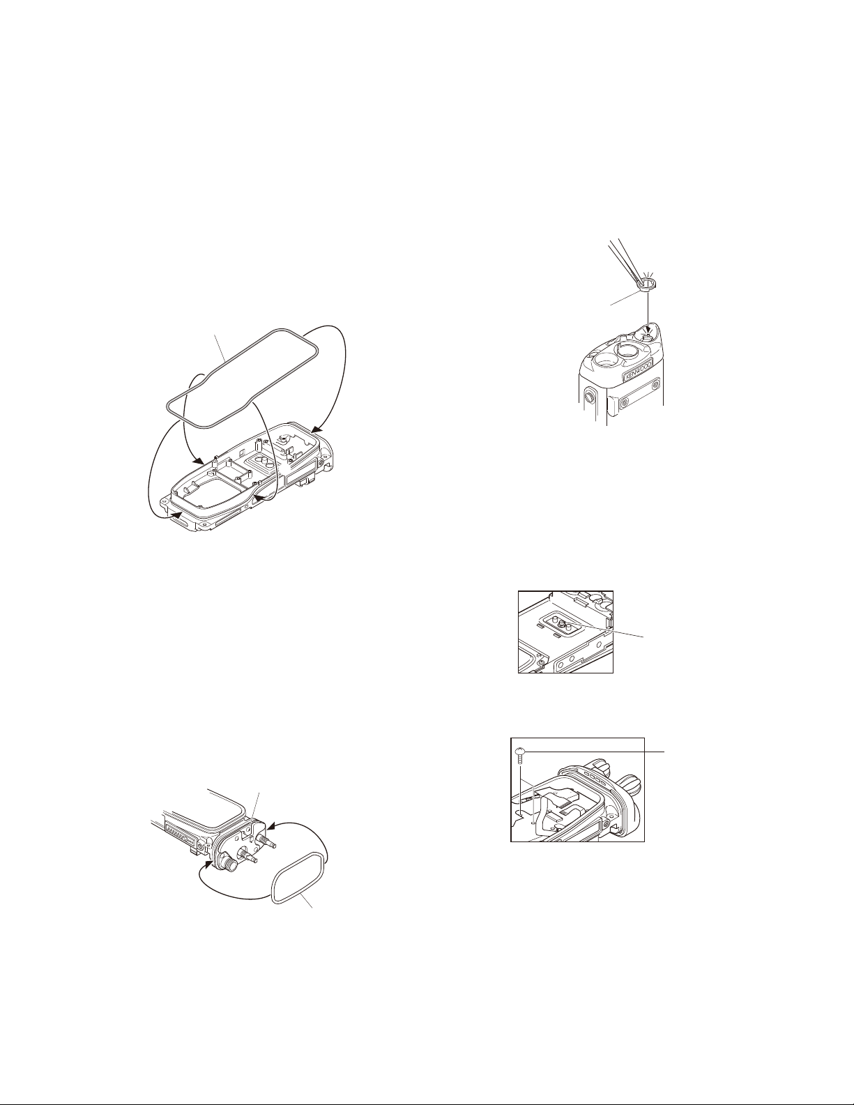
Main Packing (G53-1637-04) Installation Procedure
■
1. Hook the packing (coated with silicon oil) in the upper
groove of the chassis q, then fit the packing into the
lower groove of the chassis w.
Note:
Ensure that the chassis grooves and packing are free
from dirt and dust.
2. Fit the packing into the grooves on both sides of the
chassis e. (Fit the packing into the groove in the chassis
by tracing it lightly with your fi ngers.)
Main packing
:
.
.
@
Note:
To remove the packing from the chassis groove, use a
resin adjustment bar or other such device. If the packing
is pried with a sharp metallic tool, such as tweezers, the
packing may become damaged.
3. Verify that the packing fi ts snuggly into the groove of the
chassis.
Volume Torque-up Packing (G53-1628-04)
■
Installation Procedure
Insert the packing using a pair of tweezers so that the
hollow of the packing fi ts the convex of the panel q.
Volume torque-up packing
Screw sequence for mounting the battery
■
:
terminal block to the chassis
Attach the battery terminal block to the chassis as de-
scribed in the following procedure.
1. Loosely fi x the hexagon screws of the GND terminal to
the chassis (enough so that the hexagon screws do not
move).
3. Verify that the packing fi ts snuggly into the groove of the
chassis.
Top Packing (G53-1638-04) Installation Procedure
■
1. Ensure that the hardware fi xture is fi rst secured to the
chassis.
2. Hook the packing (coated with silicon oil) in the upper
left groove of the chassis q, then fi t the packing into the
right groove of the chassis w.
Hardware fixture
:
@
Top packing
Note:
• Verify that the chassis grooves and packing are free from
dirt and dust.
• To remove the packing from the chassis groove, use a
resin adjustment bar or other such device. If the packing
is pried with a sharp metallic tool, such as tweezers, the
packing may become damaged.
GND terminal
2. Tighten the two screws from the TX-RX PCB side.
Two screws
3. Firmly tighten the hexagon screws of the GND terminal.
15
TK-5210(G
)
DISASSEMBLY FOR REPAIR
Installation Procedure During Parts
Replacement
Attaching the Sheet (G10-1338-04, J99-0383-14)
■
to the Front Case Speaker and Installation of the
Packing (G53-1633-04)
1. Attach a new fiber sheet q (G10-1338-04) so that its
convex fi ts the hollow of the front case w.
2. Attach a new pressure sensitive adhesive sheet e (J990383-14) so that its convex fi ts the hollow of the front
case r.
3. Remove the separation sheet from the pressure sensitive adhesive sheet with a pair of tweezers t.
4. Fit the packing y (G53-1633-04) into the front case
speaker.
Note:
Fit the packing into the hollow of the case so that the
two low-height places in the convex of the packing are
positioned on the lower side u.
Installing a new LCD ASSY to the holder
■
(K2, K3 and K7 models only)
1. Remove the separation paper (brown) from the new
sheet q w, and attach the sheet to the surface of the
holder e.
2. Remove the protection sheets attached to both sides of
the new LCD ASSY.
3. Remove the separation paper (white) from the sheet in
step 1 r, then attach the LCD ASSY t to the sheet.
4. Attach two pieces of double-sided adhesive tape y to
the back of the holder and remove the separation paper.
5. Remove the protection sheet (transparent) attached to
one side of the new fi lter u i and remove the protection sheet (yellow) from the other side o.
6. Attach the fi lter from step 5 to the back of the holder.
7. Attach the new cushion !0 so that it fi ts to the corner of
the holder convex.
:
@
=
B
>
@
5. Verify that the packing does not ride on the rib of the
case.
.
;=
:
=
.
;
:
.
B
B
B
B
2
8
>
16
DISASSEMBLY FOR REPAIR
TK-5210(G
)
Procedures when Replacing the Top Panel
■
1. Insert the O-ring q into the lever switch part of the new
top panel.
2. Apply grease to the base of the shaft of the lever knob
and install the lever knob so that it is in the “●” posi-
w
tion (circle painted in white) on the top panel e.
3. Pass the hardware fi xture r through the shaft and install
it onto the top panel.
4. Apply grease to between the two holes in the hardware
fi xture r.
5. Install the hardware fi xture t so that it is inserted into
the hole on the left side of the hardware fi xture r.
6. Fix the two hardware fi xtures with the hexagon nut y.
7. Apply bond (Three Bond 1401C) to the tip of the lever
knob shaft and the surface of the hexagon nut u.
Inserted into the hole
on the left side of the
hardware fixture.
;
>
=
B
Apply bond (Three Bond 1401C)
to the tip of the lever knob shaft
and the surface of the hexagon
nut.
Apply grease to between
the two holes in
the hardware fixture.
.
@
:
Top panel
Apply grease to the
base of the shaft of
the lever knob.
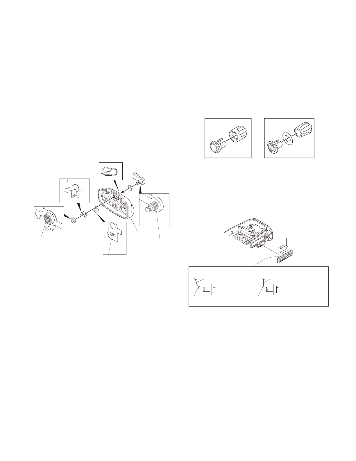
Volume Knob and Channel Knob Parts
■
Replacement
Since the volume knob consists of two components, a
knob q and a spacer w, replace and reinstall these two
parts at the same time.
Since the channel knob consists of three components, a
knob e, a 16CH display seal r and a spacer t, replace
and reinstall these three parts at the same time.
Volume Knob Channel Knob
:
@
Procedure when replacing the universal
■
=
.
;
connector FPC (J82-0097-25)
When assembling a new universal connector FPC, insert
the FPC into the chassis hole by gently bending the FPC
as shown in the fi gure.
Universal connector FPC
(J82-0097-25)
Right
Universal connector FPC
Universal
Connector
Bend the FPC gently.
Do not bend the FPC at a sharp angle.
Wrong
Universal connector FPC
Universal
Connector
17
TK-5210(G
)
CIRCUIT DESCRIPTION
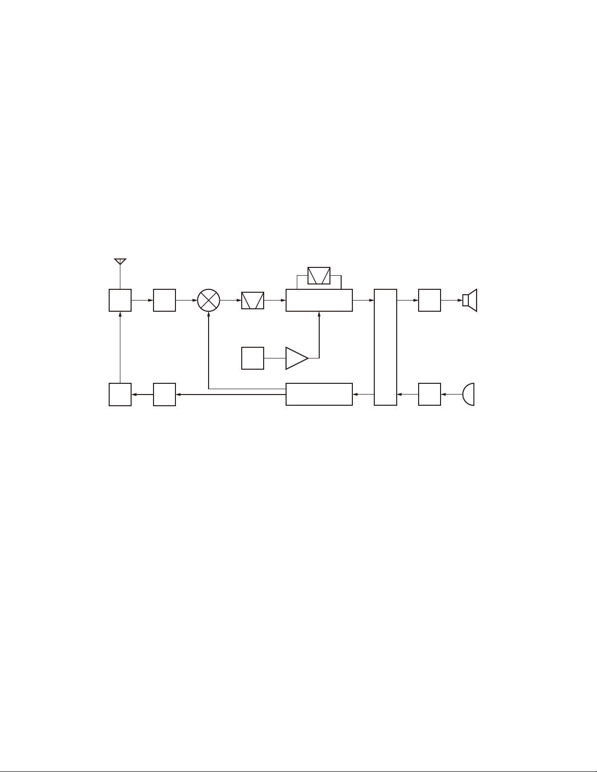
1. Overview
The KENWOOD model TK-5210(G) is a VHF/FM/P25 Portable transceiver designed to operate in the frequency range
of 136 to 174MHz.
The unit consists of a receiver, a transmitter, a phaselocked loop (PLL) frequency synthesizer, a digital control
unit, power supply circuit.
ANT
TX/RX: 136~174MHz
ANT
SW
PA
AMP
RF
AMP
TX
AMP
1st MIX
185.95~223.95MHz
136~174MHz
MCF
49.95MHz
16.8MHzx350.4MHz
VCXO
2. Frequency Confi guration
The receiver is a double-conversion super heterodyne
using first intermediate frequency (IF) of 49.95MHz and
second IF of 450kHz. Incoming signals from the antenna are
mixed with the local signal from the PLL circuit to produce
the fi rst IF of 49.95MHz.
This is then mixed with the 50.4MHz second local signal
to produce the 450kHz second IF. This signal is detected to
give the demodulated signal in the DSP.
The transmit signal frequency is generated by the PLL
VCO, and modulated by the signal from the DSP. It is then
amplifi ed and fed to the antenna.
CF
450kHz
SP
MIX
IF AMP
Base Band Circuit
PLL
VCO
AF
AMP
MIC
MIC
AMP
Fig. 1 Frequency confi guration
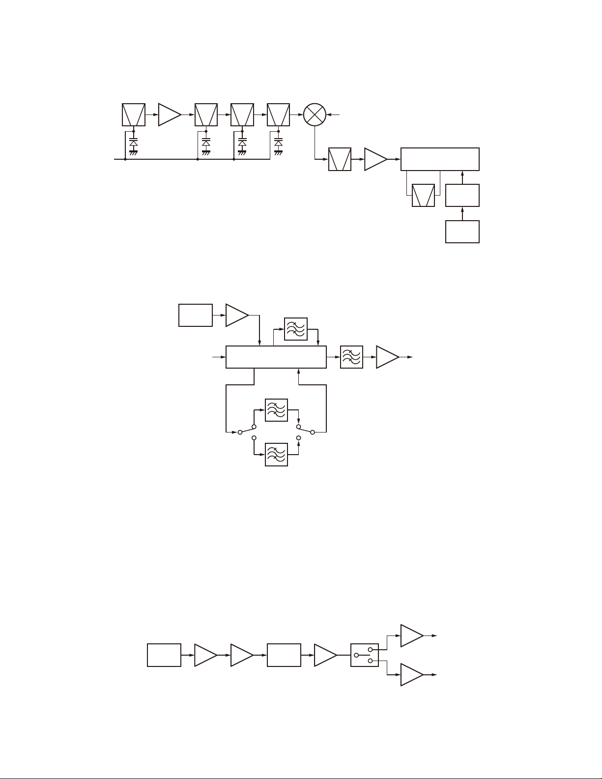
3. Receiver System
3-1. Front-end RF Amplifi er
The signal is passed through an antenna matching coil,
where the high-frequency components are amplified by a
GaAs FET (Q202). The signals are then fed into band-passfi lter that uses varactor diode tuning to reject unwanted signal
components, and is fed to the 1st mixer.
3-2. 1st Mixer
The 1st mixer is used the GaAs IC (IC202). The 1st mixer
mixes the signal with the 1st local oscillator frequency from
the VCO, and converts it to the 1st IF (49.95MHz). The signal then passes through monolithic crystal fi lter (XF201) to
remove unnecessary nearby frequency components. The
signal from the MCF is used as the 1st IF signal.
3-3. IF Amplifi er
The 1st IF signal is amplifi ed by the IF amplifi er (Q204)
and fed into the FM IC (IC204). The IF signal is then mixed
with the 2nd local oscillator frequency of 50.4MHz to generate the 2nd IF of 450kHz. The 450kHz signal is then passed
through a ceramic fi lter (CF201) and fed back into IC204 for
additional amplifi cation.
3-4. Wide/Narrow/P25 Switching Circuit
Wide, Narrow, and P25 settings can be made for each
channel by switching the ceramic filters CF203 (Wide),
CF204 (Narrow, P25), and there are controlled with the multiplexers (IC206, IC207).
When a W_/N Signal line is H, the 450kHz signal is
passed through a ceramic fi lter (CF203).
When a W_/N signal line is L, the 450kHz signal is
passed through a ceramic fi lter (CF204).
After that, the signal throughs ceramic fi lter (CF250) and
is fed into ASIC (IC10). And then, the signal is demodulated
in ASIC, the AF signal is dealed with DSP (IC3).
18
CIRCUIT DESCRIPTION
TK-5210(G
)
TUNE
L201
BPF
Q202
LNA
L202
BPF
X201
VCXO
L204
BPF
L205
BPF
IC202
MIXER
Fig. 2 Receiver section
Q205
x3
2nd Lo
CF201
IC204
FM IC
1st Local OSC
XF201
MCF
49.95MHz
CF250 IC250
Q204
IF AMP
CF201
ASIC1st IF
IC204
FM IC
2nd Local OSC
Tripler
X3
VCXO
Q205
X201
16.8MHz
CF204
Narrow/P25
IC206 IC207
CF203
Wide
Fig. 3 Wide/Narrow/P25 switching circuit
3-5. Audio Amplifi er Circuit
The AF signal from ASIC (IC10) is fi ltered for anti-aliasing
and to eliminate unwanted spectrums to hear. Next, the AF
signal goes through an electronic volume control (IC10) to
be adjusted its level and a buffering AF amplifi er IC506. Finally the AF signal into the audio power amplifi er (IC11, 12).
IC10 IC506
ASIC
IC510
IC502 IC13 IC9
DAC
The audio output can be provided to external speaker
(CN505 12pin, 13pin) or internal speaker (CN34 1pin, 2pin,
3pin, 4pin). When INAMT signal is H, AF signal loads CN34.
When EXAMT signal is H, AF signal loads CN505.
IC11
INT SP
IC12
Fig. 4 Audio amplifi er circuit
EXT SP
19
TK-5210(G
)
CIRCUIT DESCRIPTION
3-6. Squelch Circuit
It amplifies the demodulated noise signal from FM IC
(IC204) after fi ltering through BPF circuit. Then, the amplifi ed signal is converted to DC signal by the detection circuit.
The converted signal is fed to the ASIC (IC10).
4. Transmitter System
4-1. Audio Band Circuit
The signal from the microphone passes through the
mute switch (Q506) and AGC circuit (IC516, D511, D512,
Q504, Q505), and goes to the summing amplifi er (IC513),
then is fed into ASIC (IC10) and converted from analogto
digital. The digitalized signal undergoes AGC processing,
pre-emphasizing, fi ltering, vocording (in APCO mode), and
returns to the ASIC (IC10). The signal is converted from digital to analog signal is amplifi ed by ASIC (IC10). Then the signal adjusted to appropriate level passes through the buffer
(IC512) and DAC (IC502), and goes to the VCO and VCXO in
PLL section.
IC204
FM IC
Q502
Noise
AMP
D500
DET
IC10
ASIC
Fig. 5 Squelch circuit
4-2. Base Band Circuit
The audio signal output from the base band circuit is con-
verted to digital data of a sampling frequency of 48kHz.
This digital data is sent to the DSP (IC3), and voice signals of 300Hz or lower and frequencies of 3kHz or higher
are cut off and an audio range 300Hz to 3kHz is extracted.
The audio signal is then pre-emphasized in FM mode and
synthesized with the signals, such as QT and DQT, as required, and is then output from the ASIC (IC10). In Digital
mode, the audio signal is converted to the C4FM base band
signal and output from the IC10. The DTMF and MSK base
band signals are also generated by the DSP and output by
the IC10.
LPF (IC512) works as smoothing fi lter. The DAC (IC502)
assigns the base band signal to the VCO and VCXO (X301).
At this time, the level output according to the transmit carrier is fi ne-adjusted according to each modulation method.
EXT. MIC
INT. MIC
Q508
SW
SW AGCQ507
CTS0_univ MM
LPF DAC
Optional Scrambler Board
Q506
SW
IC502IC512
IC516
AMP
D511,D512
Q504,Q505
IC500
AMP
IC515
SW
/SCSW
X301
VCXO
VCO
IC513
AMP
Fig. 6 Audio band and Base band circuit
IC3
DSP
IC10
ASIC
20
CIRCUIT DESCRIPTION
TK-5210(G
)
4-3. Transmit Signal Amplifi cation Circuit
(From T/R switch to Final amplifi er)
The transmit signal passing through the T/R switch (D101)
is amplifi ed to approx 100mW by the two transistor amplification circuits (Q101, Q102). The transmit signal output
from Q102 passes through a 3dB attenuator to improve
high-frequency signal matching is amplified by the drive
amplifier (Q103) and applied to the final amplifier (Q105).
The signal applied to the fi nal amplifi er is amplifi ed by the
fi nal amplifi er so that the antenna output is 5W (1W for Low
Power).
4-4. High-Frequency Signal Switch Circuit
(From Antenna switch to ANT output)
The transmit signal output from the fi nal amplifi er (Q105)
passes through the antenna switch (D106, D107) and
LPF, and goes into the SPDT switch (IC102, IC103) which
changes the antenna connector (CN101) and the universal
connector (CN102). The transmit signal passing through the
output change switch passes through the surge protection
HPF and spurious removing LPF and then goes to the antenna connector (CN101) or the universal connector (CN102),
specifi ed by the SPDT switch (IC102, IC103).
Q102
Pre Drive
AMP
3dB
Attenuator
Q103
Drive
AMP
D101
T/R SW
Q101
Pre Pre
Drive AMP
4-5. APC circuit
The APC circuit detects the current of the drive amplifier (Q103) and final amplifier (Q105) during transmission
and controls the output power by controlling the current. It
detects the current using R119 and R120 and applies a drop
voltage between both resistors during transmission to APC
IC (IC101). It controls the transmission current of the drive
amplifi er and fi nal amplifi er so that it is constant by comparing this current with the reference voltage output from pin
7 of IC104. The reference voltage input to pin 5 of IC104 is
output from the DAC (IC502).
High/Low power output is set according to the DAC output voltage.
4-6. Temperature Protection Circuit
The temperature protection circuit reduces the APC
voltage when the temperature of Q105 rises, to prevent
thermal destruction of the fi nal amplifi er (Q105). The ASIC
(IC10) detects the temperature with a thermistor (TH101) to
control the reference voltage to the APC circuit.
Q105
Final
AMP
D106,D107
ANT SW
LPF
IC102
SPDT
IC103
SPDT
CN101
CN102
Fig. 7 Transmitter circuit
5. PLL Frequency Synthesizer
5-1. VCXO (X301)
VCXO (X301) generates a reference frequency of
16.8MHz for the PLL frequency synthesizer. This reference
frequency is applied to pin 8 of the PLL IC (IC303).
The VCXO oscillation frequency is fi ne-adjusted by controlling the voltage applied to pin 1 of the VCXO with DAC
(IC502). It is also controlled with pin 1 of the VCXO if the
output from VCXO is modulated.
5-2. VCO
There is a RX VCO and a TX VCO.
The TX VCO (Q311) generates a transmit carrier and
the RX VCO (Q310) generates a 1st local receive signal.
For the VCO oscillation frequency, the transmit carrier is
272 to 348MHz and the 1st local receive signal is 371.9 to
IC101
R119
R120
+B
APC
447.9MHz.
The VCO oscillation frequency is determined by one sys-
tem of operation switching terminal “VCOSW1” and two
systems of voltage control terminals “CV” and “ASSIST”.
The operation switching terminal, “VCOSW1", is controlled
by the ASIC (IC10). When the VCOSW1 logic is high, the RX
VCO outputs the signal. And if the logic is low, TX VCO outputs the signal.
The voltage control terminals, “CV” and “ASSIST", are
controlled by the PLL IC (IC303) and rheostat (IC414) and
the output frequency changes continuously according to the
applied voltage. For the modulation input terminal, “VCO_
MOD”, the output frequency changes according to the
applied voltage. This is used to modulate the VCO output.
“VCO_MOD” works only when transmit is active (user
pressed PTT).
APC SW
21
TK-5210(G
)
CIRCUIT DESCRIPTION
5-3. Rheostat (IC414)
The rheostat (IC414) is connected to the VCO voltage
control terminal, “V-assist”, and quickly controls the VCO
oscillation frequency. However, its accuracy is low and the
VCO frequency cannot be matched accurately with the
desired transmit carrier or the 1st local receive signal. The
rheostat is controlled by the ASIC (IC10) through the 3-lines
“PCS_pot”, “SDO0”, “SCK0” serial bus.
5-4. PLL IC (IC303)
PLL IC compares the differences in phases of the VCO
oscillation frequency and the VCXO reference frequency,
returns the difference to the VCO CV terminal and realizes
the “Phase Locked Loop” for the return control. This allows
the VCO oscillation frequency to accurately match (lock) the
desired frequency.
When the frequency is controlled by the PLL, the frequency convergence time increases as the frequency difference increases when the set frequency is changed. To
Q308,Q309
VCOSW1
TCXO_ MOD
ASSIST
IC301
Q310,Q311
VCO
LPF
IC500 VCO_MOD
SUM
IC502
DAC
AFC
IC10
ASIC
5C
15V
PCS_pot
SDO0
SCK0
CV
PLD
PCS_RF
SDO0
SCK0
Q306
BUFF
Q307
Ripple filter
Q315
Ripple filter
IC414
Rheostat
IC303
PLL IC
X301
VCXO
supplement this, the ASIC (IC10) is used before control by
the PLL IC to bring the VCO oscillation frequency close to
the desired frequency. As a result, the VCO CV voltage does
not change and is always stable at approx. 2.0V.
The desired frequency is set for the PLL IC by the ASIC
through the 3-line “PCS_RF”, “SDO0”, “SCK0” serial bus.
Whether the PLL IC is locked or not is monitored by the
ASIC through the “PLD” signal line. If the VCO is not the
desired frequency (unlock), the “PLD” logic is low.
5-5. Local Switch (D101, D210)
The connection destination of the signal output from the
1/2 driver (IC304) is changed with the diode switch (D101)
that is controlled by the transmission power supply, 5T, and
the diode switch (D210) that is controlled by the receive
power supply, 5R.
If the 5T logic is high, it is connected to a send-side prepre-drive (Q101). If the 5T logic is low, it is connected to a
receive-side mixer (IC202).
Q314
to pre-pre-drive
(Q101)
to 1st mixer
(IC202)
Q312
BUFF
IC304
1/2
BUFF
D101
SW
D210
SW
Fig. 8 PLL block diagram
6. Control Circuit
The control circuit consists of the ASIC (IC10) and its pe-
ripheral circuits. IC10 mainly performs the following;
1) Switching between transmission and reception by PTT
signal input.
2) Reading system, zone, frequency, and program data
from the memory circuit.
3) Sending frequency program data to the PLL.
4) Controlling squelch on/off by the DC voltage from the
squelch circuit.
5) Controlling the audio mute circuit by decode data input.
22
6-1. ASIC
The ASIC (IC10) is 32bit RISC processor, equipped with
peripheral function and ADC/DAC.
This CPU operates at 18.432MHz clock and 3.3V/1.5V
DC. It controls the fl ash memory, SRAM, DSP, the receive
circuit, the transmitter circuit, the control circuit, and the display circuit and transfers data to or from an external device.
CIRCUIT DESCRIPTION
TK-5210(G
)
6-2. Memory Circuit
Memory circuit consists of the ASIC (IC10) and the
SRAM (IC4), the fl ash memory (IC1). The fl ash memory has
capacity of 32M-bit that contains the transceiver control
program for the ASIC and stores the data. It also stores the
data for transceiver channels and operating parameter that
are written by the FPU. This program can be easily written
from external devices. The SRAM has capacity of 1M-bit
that contains work area and data area.
Flash memory
■
Note: The flash memory stores the data that is written
by the FPU (KPG-95DG), tuning data (Deviation, Squelch,
etc.), and fi rmware program (User mode, Test mode, Tuning
mode, etc.). This data must be rewritten when replacing the
fl ash memory.
SRAM (static memory)
■
Note: The SRAM has temporary data area and work area.
When the power supply is off, it is backed up by an internal
secondary lithium battery. Therefore, the save data does not
break.
Real-time clock
■
The clock function is based on real-time clock IC (IC7).
When the power supply is off, it is backed up by an internal
secondary lithium battery
6-7. Battery Type Detection
The transceiver automatically detects the battery type,
measuring the resistance between the S-terminal and GND
terminal on the battery pack and changes the supplied voltage to the S-terminal as below. The ASIC (IC10) then detects the battery type.
Battery type Input voltage of S-termial Resistor value
Battery case 0~0.2V Short
Li-ion battery 0.85~1.02V 47k
Ni-Cd battery 3.23~3.37V Open
Ni-MH battery 1.71~1.95V 150k
Ω
Ω
6-8. VOX
The VOX function can be used only with an external microphone.
The VOX (Voice Operated Transmission) function detects
voice input to the microphone and automatically switches
between transmission and reception. However, if a scrambler board is installed (Extended Function Voice Scrambler is
selected with FPU), VOX does not operate.
If the microphone input exceeds a certain level, transmission automatically begins. If the input falls below a certain
level, the transceiver automatically returns to receive mode.
The transceiver realizes this function using DSP (IC8).
6-3. LCD
The LCD is controlled using the bus lines on the connector (CN1) of the control unit. The LCD contrast voltage is
corrected using IC712.
6-4. Temperature Detection Circuit
The temperature detection circuit detects the temperature using a temperature IC (IC714) and corrects the thermal
characteristic change of the squelch or LCD.
6-5. Key Detection Circuit
Keys are detected using Key scan circuit in IC10.
The /KEYI* signals that are normally pulled down go high
when any key is pressed.
6-6. Low Battery Warning
The battery voltage is divided using R712 and R714 and
is detected by the ASIC (IC10). When the battery voltage
falls below the voltage set by the Low battery warning adjustment, the red LED blinks to notify the operator that it is
time to replace the battery. If the battery voltage falls even
more (approx. 5.8V), a beep sounds and transmission stops.
Low battery warning Battery condition
The red LED blinks during
transmission.
The red LED blinks and the
warning tone beeps while the
PTT switch is pressed.
The battery voltage is low but
the transceiver is still usable.
The battery voltage is low and
the transceiver is not usable to
make calls.
6-9. DSP
The DSP circuit consists of a DSP (IC3) and processes
the base band signal. The DSP operates on an external clock
of 18.432MHz (the same as the X2), the I/O section operates at 3.3V and the core section operates at 1.5V. The DSP
carries out the following processes:
• C4FM
• Analog FM pre-emphasis/de-emphasis
• Vocoder processing between audio codec and modula-
tion/demodulation
• CAI processing, such as error correction encoding
• QT/DQT encoding/decoding
• DTMF encoding/decoding
• MSK encoding/decoding
• 2-tone encoding/encoding
• Compressor/expander processing
• Transmit/receive audio fi ltering processing
• Microphone amplifi er AGC processing
• Audio mute processing
• Modulation level processing
23
TK-5210(G
)
CIRCUIT DESCRIPTION
7. Power Supply Circuit
The power supply voltage (+B) is supplied from the bat-
tery terminal, and is then passed through the fuse (F700).
If +B voltage is detected above 5.6V by the voltage detection IC (IC16), IC17 CE pin (pin 6) becomes high and IC17
outputs 3.1V (pin 3). Additionally, when VOL SW is ON, the
3.6V and 15V DC/DC converter (IC707, IC708) CE pin (pin 4)
becomes high and 3.6V power source turns ON.
The output from the 3.6V DC/DC converter (IC707) provides the power source for three regulators (IC705, IC706,
IC710) and 1.5V DC/DC converter (IC709). After these parts
became ON, Flash (IC1), DSP (IC3), SRAM (IC4), ASIC (IC10)
Q707,Q708
+B
F700
Battery
terminal
SBC
IC704
AVR IC
SBC
start to operate. After the ASIC starts up, it begins controlling three regulators (IC701, IC702, IC704) with the SBC and
/SAVE signal. And after that, one regulator (IC700) is controlled by the 5M signal.
The output voltage from IC701 is switched by 5RC signal
(which is turned on while receiving) or 5TC signal (which is
turned on while transmitting). These signals are controlled
by the ASIC (IC10).
The output voltage from IC700 is controlled by Q703
and Q704, and is used as a power source for 5MCS, for an
optional accessory which is connected to the universal connector (CN505).
SB
IC713
Switched
Capacitor Voltage
Doubling Inverter
IC700
AVR IC
IC712
LCDCNT
DAC6
5M
Q703,Q704
5MCS
5UC
SBC
/SAVE
36MC
IC701
AVR IC
IC702
AVR IC
IC707
DCDC
IC706
AVR IC
IC705
AVR IC
IC710
AVR IC
IC709
DCDC
IC708
DCDC
5C
33C
33M
33A
15M
15V
Q700
5T
5TC
Q701
5R
5RC
24
36MC
Fig. 9 Power supply circuit

CIRCUIT DESCRIPTION
8. Signaling Circuit
8-1. Encode (QT/DQT/DTMF/2TONE /MSK)
Each signaling data signal of QT, DQT, DTMF, 2TONE and
MSK is generated by the DSP circuit, superposed on a modulation signal and output from IC10. The modulation balance
of the QT/DQT signal is adjusted by the D/A converter (IC502)
and the resulting signal is routed to the modulation input of
the VCO and VCXO (X301). The each deviation of the TX QT,
DQT, DTMF, 2TONE and MSK tone is adjusted by changing
the output level of the IC108 and the resulting signal is routed to VCO and VCXO. The RX DTMF tone is routed to the
receive audio signal system, and is output from the speaker.
8-2. Decode (QT/DQT/DTMF/2TONE/MSK)
The audio signal is removed from the FM detection signal by ASIC (IC10), and resulting signal is decoded by DSP
(IC3).
9. Compander Circuit
The term “compander” means compressor and expander. The compander reduces noise by utilizing a compressor
and an expander. The transceiver contains a DSP (IC3) to
perform this operation. The transceiver compander can be
turned on or off using the FPU.
TK-5210(G
)
25

TK-5210(G
)
COMPONENTS DESCRIPTION
Control unit (X53-4390-XX)
Ref. No. Part Name Description
IC1 IC Flash memory
IC3 IC DSP
IC4 IC Static memory
IC5 IC Voltage detector (RST)
IC6 IC Buffer AMP (Logic)
IC7 IC Real-time clock
IC8 IC Clock buffer AMP
IC9 IC Bus buffer (LCD)
IC10 IC ASIC
IC11,12 IC Audio AMP (BTL)
IC13 IC
IC15 IC I/O Expander
IC16 IC Voltage Detector (/BINT)
IC17 IC Voltage regulator (3.1V)
IC18 IC Bus buffer (LCD)
IC19 IC 5V to 3.3V Level convertor
Q1,2 Transistor AVR for backlight LED
Q3 Transistor 5A AVR
Q4 FET DC switch (5AC)
Q5 Transistor 5A AVR
Q6 Transistor Echo cancel MIC switch
Q7,8 FET DC switch (/BINT, PSW)
Q10,11 FET DC switch (BLED, TXLED)
Q12 Transistor DC switch (36MC)
Q13 Transistor DC switch
Q14 FET DC switch (31BU)
Q15 FET DC switch (STCAMI)
Q16 Transistor DC switch
D1 Zener diode AVR for backlight LED
D2~5 LED Key backlight
D6~8 LED LCD backlight
D9~12 LED Key backlight
D13~16 Diode Reverse current prevention
D19,20,22 Varistor Surge absorption
D23~26 Diode Reverse current prevention
D27 Varistor Surge absorption
Audio AMP (1/2 Audio pre-AMP,
2/2 NC MIC AMP)
TX-RX unit (X57-7650-10 A/4)
Ref. No. Part Name Description
IC101 IC Auto power control
IC102,103 IC SPDT
IC104 IC DC AMP for APC
IC201 IC DC AMP for BPF
IC202 IC DBM
IC204 IC FM IC
IC206,207 IC Multiplexer
IC250 IC IF AMP
IC301 IC DC AMP for VCO tune
IC303 IC PLL IC
IC304 IC 1/2 Divider
IC414 IC Rheostat
IC500 IC Buffer AMP (AFC/TCXO_MOD)
IC501 IC 5V to 3.3V Level converter
IC502 IC DAC
IC503
IC505 IC I/O Expander
IC506 IC Buffer AMP (AF)
IC507~509
IC510 IC DC AMP/Summing AMP
IC511 IC Logic switch
IC512 IC Buffer AMP (Mod)
IC513 IC Buffer AMP (MIC)
IC514 IC Buffer AMP (VOX)
IC515 IC MIC switch (/SCSW)
IC516 IC Buffer AMP (MIC/VOX)
IC517 IC 3.3V to 5V Level converter
IC700 IC AVR (5MCS)
IC701 IC AVR (5T/5R)
IC702 IC AVR (5C)
IC704 IC AVR (5M)
IC705 IC AVR (33M)
IC706 IC AVR (33C)
IC707 IC DC/DC converter (3.6V)
IC708 IC DC/DC converter (15V)
IC709 IC DC/DC converter (1.5V)
IC710 IC AVR (33A)
IC712 IC DC AMP (LCDCNT)
IC713 IC DC/DC converter
IC714 IC Temperature detection
IC BPF Amp for SQL voltage
IC AF pass control
26
COMPONENTS DESCRIPTION
TK-5210(G
)
Ref. No. Part Name Description
Q101,102 Transistor RF AMP
Q103 FET RF AMP (Drive AMP)
Q104 FET APC switch
Q105 FET RF AMP (fi nal AMP)
Q106 Transistor APC switch
Q107 FET APC switch
Q110 FET SPDT EXT/INT switch
Q111 Transistor 3.3V→5V level converter
Q201 Transistor Ripple fi lter
Q202 FET RF AMP (Low Noise Amp)
Q204 FET IF AMP
Q205 Transistor 2nd local buffer AMP
Q209 Transistor W/N switch
Q306 FET Buffer for CV
Q307 Transistor Ripple fi lter
Q308,309 FET T/R switch for VCO
Q310,311 FET VCO
Q312~314 Transistor Buffer AMP
Q315 Transistor Ripple fi lter
Q316 FET Switch for PLL IC
Q417 FET APC switch
Q502 Transistor SQL AMP
Q503 FET TONE switch
Q504,505 Transistor MIC AGC
Q506 FET MIC mute switch
Q507,508 FET Int/Ext MIC switch
Q509 FET DC switch
Q700 FET 5T control switch
Q701 FET 5R control switch
Q703 FET 5MCS control switch
Q704 FET 5MCS control switch
Q705 FET DC/DC (15V)
Q706 FET DC/DC (3.6V)
Q707,708 FET DC switch
Q709 FET 15V switch
Ref. No. Part Name Description
D101 Diode Local switch
D105 Zener diode Voltage protection
D106~109 Diode Antenna switch
D110,111 Varistor Surge absorption
Variable
D202~209
D210 Diode Local switch
D303,304
D306~312
D313 Diode Ripple fi lter
D314 Diode Bypass diode
D500 Diode Noise Detect
D501 Diode PLD
D502,504 Zener diode Surge absorption
D505 Diode /PTT Terminal Protection
D510 Diode VOX Detect
D511,512 Diode MIC AGC
D515,516 Varistor Surge absorption
D517 Diode VOX DC
D518,519 Diode RXD1
D521 Diode OPT6
D700 Diode Reverse Battery Protection
D702 Diode BaTT Terminal Protecrion
D704 Diode AVR CE (IC705, IC706, IC710)
D706 Diode DC/DC converter (3.6V)
capacitance
diode
Variable
capacitance
diode
Variable
capacitance
diode
Vari-cap tune
Frequency control
Frequency control
Top Panel unit (X57-7650-10 B/4)
Ref. No. Part Name Description
D901 LED TX/RX LED
27
TK-5210(G
)
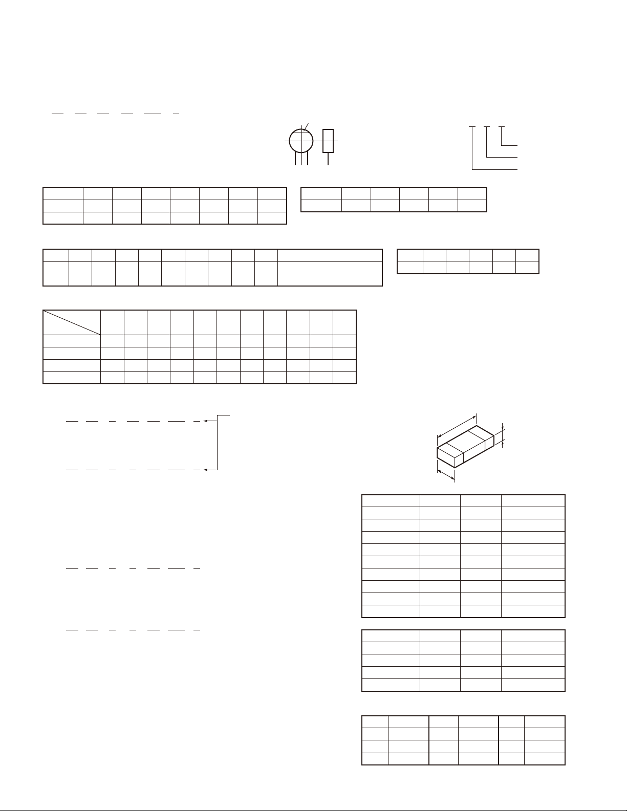
#!0!#)4/23
C C 4 5 T H 1 H 2 2 0 J
1 2 3 4 5 6
1 = Type ... ceramic, electrolytic, etc. 4 = Voltage rating
2 = Shape ... round, square, etc. 5 = Value
3 = Temp. coefficient 6 = Tolerance
s4EMPERATURECOEFFICIENT
1st Word C L P R S T U
Color* Black Red Orange Yellow Green Blue Violet
ppm/°C 0 –80 –150 –220 –330 –470 –750
PARTS LIST
CC45
Color*
2nd Word G H J K L
ppm/°C ±30 ±60 ±120 ±250 ±500
Example : CC45TH = –470±60ppm/°C
s#APACITORVALUE
010 = 1pF 2 2 0 = 22pF
100 = 10pF
101 = 100pF Multiplier
102 = 1000pF = 0.001μF 2nd number
103 = 0.01μF 1st number
s4OLERANCE-ORETHANP&
Code C D G J K M X Z P No code
(%) ±0.25 ±0.5 ±2 ±5 ±10 ±20 +40 +80 +100 More than 10μF : –10~+50
–20 –20 –0 Less than 4.7μF : –10~+75
s6OLTAGERATING
2nd word
1st word
0 1.0 1.25 1.6 2.0 2.5 3.15 4.0 5.0 6.3 8.0 –
1 10 12.5 16 20 25 31.5 40 50 63 80 35
2 100 125 160 200 250 315 400 500 630 800 –
3 1000 1250 1600 2000 2500 2150 4000 5000 6300 8000 –
s#HIPCAPACITORS
(EX) C C 7 3 F S L 1 H 0 0 0 J Refer to the table above.
1 2 3 4 5 6 7 1 = Type
(Chip) (CH, RH, UJ, SL) 2 = Shape
3 = Dimension
(EX) C K 7 3 F F 1 H 0 0 0 Z 4 = Temp. coefficient
1 2 3 4 5 6 7 5 = Voltage rating
(Chip) (B, F) 6 = Value
7 = Tolerance
2%3)34/23
s#HIPRESISTOR#ARBON
(EX) R D 7 3 E B 2 B 0 0 0 J
1 2 3 4 5 6 7
(Chip) (B, F)
s#ARBONRESISTOR.ORMALTYPE
(EX) R D 1 4 B B 2 C 0 0 0 J
1 2 3 4 5 6 7
1 = Type 5 = Rating wattage
2 = Shape 6 = Value
3 = Dimension 7 = Tolerance
4 = Temp. coefficient
A B C D E F G H J K V
s$IMENSION
Chip capacitor
Code L W T
Empty 5.6±0.5 5.0±0.5 Less than 2.0
A 4.5±0.5 3.2±0.4 Less than 2.0
B 4.5±0.5 2.0±0.3 Less than 2.0
C 4.5±0.5 1.25±0.2 Less than 1.25
D 3.2±0.4 2.5±0.3 Less than 1.5
E 3.2±0.2 1.6±0.2 Less than 1.25
F 2.0±0.3 1.25±0.2 Less than 1.25
G 1.6±0.2 0.8±0.2 Less than 1.0
H 1.0±0.05 0.5±0.05 0.5±0.05
Chip resistor
Code L W T
E 3.2±0.2 1.6±0.2 1.0
F 2.0±0.3 1.25±0.2 1.0
G 1.6±0.2 0.8±0.2 0.5±0.1
H 1.0±0.05 0.5±0.05 0.35±0.05
s2ATINGWATTAGE
Code Wattage Code Wattage Code Wattage
1J 1/16W 2C 1/6W 3A 1W
2A 1/10W 2E 1/4W 3D 2W
2B 1/8W 2H 1/2W
,ESSTHANP&
Code B C D F G
(pF) ±0.1 ±0.25 ±0.5 ±1 ±2
L
T
W
28

PARTS LIST
TK-5210(G
)
New Parts.
✽
Parts without Parts No. are not supplied.
Les articles non mentionnes dans le Parts No. ne sont pas fournis.
Teile ohne Parts No. werden nicht geliefert.
Ref. No.
indicates safety critical components.
New
Ad dress
Parts No. Description
parts
Desti-
nation
TK-5210(G)
1 1B A02-3875-01 MAIN CABINET K
2 1D A02-3877-11 MAIN CABINET (4KEY) K2K7
3 1D A02-3879-11 MAIN CABINET (DTMF) K3
4 3A,3C A10-4084-51 CHASSIS
5 2B,2D A62-1104-02 PANEL (TOP)
7 3A,3C A82-0057-02 REAR PANEL
9 2B,2D B03-3612-04 DRESSING PLATE (SELECTOR)
10
11 2B,2D B11-1821-03 ILLUMINATION GUIDE (TX-BUSY)
12 1C B11-1832-04 FILTER (LCD) K2K3K7
13 1C B38-0929-05 LCD K2K3K7
15 3A,3C B41-1841-04 CAUTION STICKER
16 1B,1D B43-1171-04 BADGE (FRONT)
17 2B,2D B43-1172-04 BADGE (REAR)
18 2F B59-2596-00
19 2E B62-2155-00 INSTRUCTION MANUAL (ENG/FRE)
21 2A,2C E37-0722-05 LEAD WIRE WITH CONNECTOR (UNIV)
22 2B,2D E37-1126-25 LEAD WIRE WITH CONNECTOR (ANT)
23 3B,3D E58-0510-15 RECTANGULAR RECEPTACLE (UNIV)
24 3A,3C E72-0420-33 TERMINAL BLOCK
26 3A,3C F07-1887-22 COVER ASSY
27 2A,2B F10-3104-03 SHIELDING CASE (CONT-B)
28 2A,2B F10-3114-03 SHIELDING CASE (TXRX-A UPPER)
29 2A,2B F10-3115-04 SHIELDING CASE (TXRX-A BOTTOM)
31 3A,3C G10-1327-04 FIBROUS SHEET (AIR)
32 1B,1D G10-1338-04 FIBROUS SHEET (SP)
33 1C G10-1346-04 FIBROUS SHEET (LCD FPC) K2K3K7
34 3A,3C G10-1366-04 FIBROUS SHEET (BACKPANEL)
35 1C G11-4302-04 SHEET (LCD) K2K3K7
37 3A,3C G11-4303-14 SHEET (PTT)
38
39 3B,3D G11-4346-08 SHEET (UNIV)
40 2B,2D G11-4490-04 SHEET (ANT)
41
43 3A,3C G13-1941-04 CUSHION (CHASS/PCB)
44 1A,1C G13-2036-04 CUSHION (MIC)
45
46 3A,3C G13-2070-04 CUSHION (OPB)
47 2A,2C G13-2071-04 CONDUCTIVE CUSHION (CHASS/PCB)
49
50 1C G13-2087-14 CUSHION (LCD) K2K3K7
51 2A,2C G13-2284-04 CUSHION (CORD ASSY)
52 2B,2D G53-1628-04 PACKING (VOLTORQ-UP)
53 2B,2D G53-1629-05 PACKING (VOL,SEL O-RIG)
55 2B,2D G53-1630-05 PACKING (ANT O-RIG)
56 2B,2D G53-1631-05 PACKING (LEVER SW O-RING)
57 1B,1D G53-1633-04 PACKING (SP)
58
59 2A,2C G53-1637-04 PACKING (MAIN)
61 2B,2D G53-1638-04 PACKING (TOP)
62 3A,3C G53-1640-03 PACKING (BATT)
63 3A,3C G53-1649-05 PACKING (TERMINAL O-RING)
64 3A,3C G53-1663-23 PACKING (TERMINAL BLOCK)
1B,1D,1E
B09-0682-13 CAP (SP/MIC) ACCESSOY
SUB-INSTRUCTION MANUAL (QRC E/F)
1B,1D,2F
G11-4340-04 RUBBER SHEET (CAP) ACCESSORY
1B,1D,2A,2C
G11-4526-04 SHEET (MIC)
2A,2C,3B,3D
G13-2046-04 CUSHION (UNIV)
2A,2B,2C,2D
G13-2079-04 CUSHION (VOL)
1B,1D,2A,2C
G53-1634-14 PACKING (MAIN MIC,NC MIC)
L : Scandinavia K : USA P : Canada
Y : PX (Far East, Hawaii) T : England E : Eu rope
C : China X : Australia M : Oth er Areas
TK-5210(G)
Ref. No.
66 1F H12-3169-05 PACKING FIXTURE
67 3F ✽ H52-2179-12 ITEM CARTON CASE
69 1C J19-5475-12 HOLDER (LCD) K2K3K7
70 2B,2D J19-5477-04 HOLDER (EMG)
71 2B,2D J21-8482-13 MOUNTING HARDWARE (TOP)
72 2B,2D J21-8483-13 MOUNTING HARDWARE (SP)
73 3A,3C J21-8484-04 MOUNTING HARDWARE (NC MIC)
75 2B,2D J21-8495-04
76 2B,2D J21-8581-04 MOUNTING HARDWARE (LEVER)
77 2E J29-0730-05 BELT CLIP ACCESSORY
78 2B,2D J39-0646-03 SPACER (VOL)
79 2B,2D J39-0647-03 SPACER (SELECTOR)
81 3B,3D J82-0097-25 FPC (UNIV)
82 2B,2D J82-0098-05 FPC (SP/MIC)
83 2A,2C J87-0011-05 FPC (LEAD FREE/CONT-TOP)
84 2B,2D ✽ J87-0025-05 FPC (LEAD FREE/VOL.SEL)
85 3A,3C J99-0377-14 ADHESIVE SHEET (PTT)
87 3A,3C J99-0380-04 ADHESIVE SHEET (ANT PCB)
88 1B,1D J99-0383-14 ADHESIVE SHEET (SP)
89 1C J99-0390-04 ADHESIVE SHEET (LCD FILTER) K2K3K7
91 2B,2D K29-9319-03 KEY TOP (EMG)
92 1D K29-9320-03 KEY TOP (4KEY) K2K7
93 1C K29-9321-13 KEY TOP (DTMF) K3
94 2B,2D K29-9322-03 KNOB (VOL)
95 2B,2D K29-9323-03 KNOB (SELECTOR)
97 2B,2D K29-9324-13 KNOB (CONCENTRIC SW)
98 1B,1D K29-9325-04 KNOB (LEVER SW)
99 1A,1C K29-9327-03 KEY TOP (PTT)
100 1A,1C K29-9328-02 KNOB (PTT)
A
B 2B,2D N09-2439-25 SPECIAL SCREW (SP)
C 3A,3C N09-2441-25 SPECIAL SCREW (COVER ASSY)
D 2B,2D N09-2442-15 SPECIAL SCREW (ANT)
E 3A,3C N09-2443-14 HEXAGON HEAD SCREW (TERMINAL)
F 3A,3C N09-6574-05 SPECIAL SCREW (CASE)
G 2B,2D N14-0813-14 CIRCULAR NUT (VOL)
H 2B,2D N14-0814-14 CIRCULAR NUT (SEL)
J 2B,2D N14-0815-04 CIRCULAR NUT (ANT)
K 2B,2D N14-0817-14 HEXAGON NUT (LEVER SW)
L 2E N30-3008-60
M 2B,2D N32-2004-48 FLAT HEAD MACHINE SCREW (TOP)
N
O 2B,2D N83-2006-43 PAN HEAD TAPTITE SCREW (TOP)
102 3B,3D R31-0654-05 VARIABLE RESISTOR (VOL)
104 2B,2D S60-0431-15 ROTARY SWITCH (SEL)
105 1C S79-0454-05 KEYBOARD ASSY (4KEY&DTMF) K2K3K7
107 1B,1D T07-0755-15 SPEAKER
108
110 1B,1D W09-0971-05 LITHIUM CELL
112 3A,3C X41-3690-10 SWITCH UNIT (FPC (PTT))
113 2A,2C X42-3370-10 CORD ASSY (FPC (100P))
New
Ad dress
1B,1D,2E
N08-0531-14 DRESSED SCREW (CAP) ACCESSORY
1A,2A,1C,2C
N83-2005-48
2A,2B,2C,2D
T91-0575-05 MIC ELEMENT (MAIN MIC,NC MIC)
Parts No. Description
parts
MOUNTING HARDWARE (LEVER PANEL)
PAN HEAD MACHINE SCREW (BELT CLIP)
PAN HEAD TAPTITE SCREW (CONT/TXRX)
Destination
29

TK-5210(G
)
PARTS LIST
TK-5210(G)
CONTROL UNIT (X53-4390-XX)
Ref. No.
- ✽ X53-4390-13 SERVICE CONTROL UNIT K
- X53-4390-14 SERVICE CONTROL UNIT K2K7
- X53-4390-15 SERVICE CONTROL UNIT K3
CONTROL UNIT (X53-4390-XX)
D2-5 B30-2171-05 LED K3
D5 B30-2171-05 LED K2K7
D6-8 B30-2261-05 LED K2K3K7
D9-12 B30-2171-05 LED K3
D12 B30-2171-05 LED K2K7
C12-15 CK73HB1A104K CHIP C 0.10UF K
C16 CK73HB0J105K CHIP C 1.0UF K
C17 CK73HB1E103K CHIP C 0.010UF K
C18,19 CK73HB1A104K CHIP C 0.10UF K K2K3K7
C19 CK73HB1A104K CHIP C 0.10UF K K
C21,22 CK73HB1H102K CHIP C 1000PF K
C23 CK73HB1A104K CHIP C 0.10UF K
C24 CC73HCH1H101J CHIP C 100PF J K2K3K7
C25 CK73HB1A104K CHIP C 0.10UF K
C27 CK73HB1A104K CHIP C 0.10UF K
C29 CK73HB1A104K CHIP C 0.10UF K
C30 CK73HB1E103K CHIP C 0.010UF K
C31 CK73HB1A104K CHIP C 0.10UF K
C32 CK73HB1E103K CHIP C 0.010UF K
C33 CK73HB0J105K CHIP C 1.0UF K
C34 CK73HB1A104K CHIP C 0.10UF K
C35 CK73HB0J105K CHIP C 1.0UF K
C36 CK73HB1A104K CHIP C 0.10UF K
C37 CK73HB1E103K CHIP C 0.010UF K
C38,39 CK73HB1A104K CHIP C 0.10UF K
C40 CK73HB1E103K CHIP C 0.010UF K
C44 CK73HB1E682K CHIP C 6800PF K
C47 CK73HB1E103K CHIP C 0.010UF K
C48 CK73HB1A104K CHIP C 0.10UF K
C49 CK73GB0J106K CHIP C 10UF K
C50-55 CK73HB1A104K CHIP C 0.10UF K
C56 CK73HB1E103K CHIP C 0.010UF K
C57,58 CK73GB1E105K CHIP C 1.0UF K
C59,60 CC73HCH1H101J CHIP C 100PF J
C61 CK73HB1H102K CHIP C 1000PF K
C62 CK73HB1E103K CHIP C 0.010UF K
C63 CK73HB0J105K CHIP C 1.0UF K
C64,65 CK73HB1A104K CHIP C 0.10UF K
C66 CK73HB1E682K CHIP C 6800PF K
C67 CK73HB1A104K CHIP C 0.10UF K
C68 CK73GB0J106K CHIP C 10UF K
C69 CC73HCH1H101J CHIP C 100PF J
C70,71 CK73HB1A104K CHIP C 0.10UF K
C72 CC73HCH1H030C CHIP C 3.0PF C
C73 CK73HB1E103K CHIP C 0.010UF K
C74 CK73HB0J105K CHIP C 1.0UF K
C75-78 CK73HB1A104K CHIP C 0.10UF K
C79 CK73HB1E103K CHIP C 0.010UF K
C80 CK73HB0J105K CHIP C 1.0UF K
C81-85 CK73HB1A104K CHIP C 0.10UF K
C86 CC73HCH1H101J CHIP C 100PF J
C87 CK73HB1A104K CHIP C 0.10UF K
Ad dress
New
Parts No. Description
parts
Destination
-10: K -11: K2,K7 -12: K3
Ad dress
New
Parts No. Description
parts
Ref. No.
C88 CK73HB1H102K CHIP C 1000PF K
C90 CK73HB1A104K CHIP C 0.10UF K
C91 CK73HB1H102K CHIP C 1000PF K
C92 CK73HB1A104K CHIP C 0.10UF K
C93 CK73HB0J105K CHIP C 1.0UF K
C94 CK73HB0J474K CHIP C 0.47UF K
C95 CK73HB1H102K CHIP C 1000PF K
C96 CK73HB0J474K CHIP C 0.47UF K
C97-100 CK73HB1H471K CHIP C 470PF K
C101 CK73HB1A104K CHIP C 0.10UF K
C102 CK73HB1H471K CHIP C 470PF K
C103-111 CK73HB1H472K CHIP C 4700PF K
C112 CK73HB1A104K CHIP C 0.10UF K
C113,114 CK73GB0J106K CHIP C 10UF K
C115 CK73HB1H471K CHIP C 470PF K
C116 CK73HB0J105K CHIP C 1.0UF K
C117 CK73GB1E105K CHIP C 1.0UF K
C118,119 CK73HB1E103K CHIP C 0.010UF K
C120 CK73HB1H472K CHIP C 4700PF K
C121,122 CK73HB1E103K CHIP C 0.010UF K
C136,137 CK73HB1A104K CHIP C 0.10UF K
C141 CK73HB1A104K CHIP C 0.10UF K
C143 CK73HB1A104K CHIP C 0.10UF K K2K3K7
C144 CC73HCH1H221J CHIP C 220PF J K2K3K7
C146,147 CK73HB1A104K CHIP C 0.10UF K K2K3K7
C148-152 CK73HB0J105K CHIP C 1.0UF K K2K3K7
C153 CK73HB1A104K CHIP C 0.10UF K K
C153,154 CK73HB1A104K CHIP C 0.10UF K K2K3K7
C155 CK73HB1H102K CHIP C 1000PF K
C156 CC73HCH1H470J CHIP C 47PF J
C157 CC73HCH1H101J CHIP C 100PF J
C161 CK73HB1E103K CHIP C 0.010UF K
C997 CK73HB1H102K CHIP C 1000PF K K
C998 CK73HB1H102K CHIP C 1000PF K K2K7
C999 CK73HB1H102K CHIP C 1000PF K K3
CN1 ✽ E40-6884-05 FLAT CABLE CONNECTOR K2K3K7
CN34 E41-3183-05 FLAT CABLE CONNECTOR
CN35 E40-6755-05 FLAT CABLE CONNECTOR
CN38 ✽ E40-6777-05 FLAT CABLE CONNECTOR
CN40 E40-6846-05 PIN ASSY
CN37 J19-5386-05 HOLDER
L4-6 L92-0444-05 CHIP FERRITE
L7,8 L92-0162-05 BEADS CORE
L9 L92-0444-05 CHIP FERRITE
L10 L92-0149-05 CHIP FERRITE
L11,12 L92-0467-05 CHIP FERRITE
L13 L92-0163-05 BEADS CORE
L14,15 L92-0467-05 CHIP FERRITE
L16,17 L92-0444-05 CHIP FERRITE
L19 L92-0444-05 CHIP FERRITE
L20,21 L92-0163-05 BEADS CORE
L22,23 L92-0446-05 BEADS CORE
L24,25 L92-0162-05 BEADS CORE K2K3K7
L25 L92-0162-05 BEADS CORE K
L27 L92-0446-05 BEADS CORE
X1 L77-1802-05 CRYSTAL RESONATOR (32.768KHZ)
X2 L77-3015-05 TCXO (18.432MHZ)
R5 RK73HB1J474J CHIP R 470K J 1/16W
Destination
30
 Loading...