

Kenwood TK-2317 M3, TK-3317, TK-3317 M3, TK-3317 M4 Service Manual
VHF FM TRANSCEIVER
TK-2317
SERVICE MANUAL
M3 version
Helical antenna
(T90-1050-05)
Knob (Selector)
(K29-9427-03)
Knob (Volume)
(K29-9309-13)
© 2011-4 PRINTED IN JA PAN
B51-8972-00 (Y) PDF
CONTENTS
GENERAL ....................................................2
SYSTEM SET-UP .........................................3
REALIGNMENT ...........................................3
DISASSEMBLY FOR REPAIR .....................9
CIRCUIT DESCRIPTION ...........................12
SEMICONDUCTOR DATA .........................17
COMPONENTS DESCRIPTION ................18
PARTS LIST ...............................................19
EXPLODED VIEW ......................................27
Button knob (PTT)
(K29-9425-03)
Button knob
(SIDE1/SIDE2)
(K29-9426-03)
Key top (7key)
(K29-9463-12)
Plastic cabinet assy
(A02-4095-23)
PACKING ...................................................28
ADJUSTMENT ...........................................29
PC BOARD
TX-RX UNIT (X57-7880-21) ....................34
SCHEMATIC DIAGRAM ............................38
BLOCK DIAGRAM .....................................44
LEVEL DIAGRAM ......................................46
OPTIONAL ACCESSORIES
KNB-29N (Ni-MH Battery Pack) ............47
KNB-45L (Li-ion Battery Pack) .............47
KNB-53N (Ni-MH Battery Pack) ............47
KMC-48GPS (GPS Speaker Microphone)
..47
SPECIFICATIONS ..................BACK COVER
This product complies with the
directive for the European market
RoHS
.
This product uses Lead Free solder
.

TK-2317
Document Copyrights
Copyright 2011 by Kenwood Corporation. All rights re-
served.
No part of this manual may be reproduced, translated,
distributed, or transmitted in any form or by any means, electronic, mechanical, photocopying, recording, or otherwise,
for any purpose without the prior written permission of Kenwood.
Disclaimer
While every precaution has been taken in the preparation of this manual, Kenwood assumes no responsibility
for errors or omissions. Neither is any liability assumed for
damages resulting from the use of the information contained
herein. Kenwood reser ves the right to make changes to any
products herein at any time for improvement purposes.
Firmware Copyrights
The title to and ownership of copyr ights for firmware
embedded in Kenwood product memories are reserved for
Kenwood Corporation. Any modifying, reverse engineering,
copy, reproducing or disclosing on an Internet website of the
fi rmware is strictly prohibited without prior written consent of
Kenwood Corporation. Furthermore, any reselling, assigning
or transferring of the fi rmware is also strictly prohibited without embedding the fi rmware in Kenwood product memories.
GENERAL
INTRODUCTION
SCOPE OF THIS MANUAL
This manual is intended for use by experienced tech ni cians familiar with similar types of commercial grade com mu ni ca tions equipment. It contains all required service
in for ma tion for the equipment and is current as of the publication date. Changes which may occur after publication
are covered by either Service Bulletins or Manual Revisions.
These are is sued as required.
ORDERING REPLACEMENT PARTS
When ordering replacement parts or equipment in for ma tion, the full part identifi cation number should be in clud ed.
This applies to all parts : components, kits, or chassis. If the
part number is not known, include the chassis or kit number
of which it is a part, and a suffi cient description of the re quired component for proper identifi cation.
PERSONAL SAFETY
The following precautions are recommended for personal
safety:
• DO NOT transmit until all RF connectors are verifi ed se cure and any open connectors are properly terminated.
• SHUT OFF and DO NOT operate this equipment near
elec tri cal blasting caps or in an explosive atmosphere.
• This equipment should be serviced by a qualifi ed tech ni cian only.
SERVICE
This transceiver is designed for easy servicing. Refer
to the sche mat ic diagrams, printed circuit board views, and
align ment procedures contained within.
Model Type TX-RX unit
TK-2317 M3 X57-7880-21 216~223MHz
Frequency
range
Remarks
IF1: 49.95MHz
LOC: 50.4MHz
2
Merchandise received
Choose the type of transceiver
TK-2317
SYSTEM SET-UP
Frequency range (MHz) RF power Type
TX/RX 216~223 5.0W TK-2317 M3
Transceiver programming
Are you using the speaker microphone?
NO
Delivery
REALIGNMENT
A personal computer, programming interface (KPG-22A/22U),
and FPU (programming software) are required for programming.
(The frequency, TX power HI/LOW, and signaling data are
programmed for the transceiver.)
YES
KMC-21, KMC-45 or KMC-48GPS
Speaker microphone
(Option)
1. Modes
User mode
PC mode
PC test mode
Wireless clone mode
Firmware version information mode
Self-programming mode
Mode Function
User mode For normal use.
PC mode
Used for communication between the transceiver and PC.
Data programming mode
PC tuning mode
Mode Function
Data programming
mode
PC test mode
Wireless clone
mode
Firmware version
information mode
Self-programming
mode
Used to read and write frequency data and
other features to and from the transceiver.
Used to check the transceiver using the PC.
This feature is included in the FPU.
Used to transfer programming data from one
transceiver to another.
Used to confi rm the internal fi rmware version.
You can program the frequency signaling and
other function using only the transceiver.
2. How to Enter Each Mode
Mode Operation
User mode Power ON
PC mode Received commands from PC
Wireless clone mode [<B] + Power ON (Two seconds)
Firmware version
information mode
Self-programming mode [S] + Power ON (Two seconds)
[Side1] + [Side2] + Power ON (Two
seconds)
3
TK-2317
REALIGNMENT
3. PC Mode
3-1. Preface
The transceiver is programmed by using a personal computer, a programming interface (KPG-22A/22U, USB adapter
(KCT-53U)) and programming software (KPG-134D: ver. 1.20
or later).
The programming software can be used with a PC. Figure 1 shows the setup of a PC for programming.
3-2. Connection Procedure
1. Connect the transceiver to the personal computer with
the interface cable and USB adapter (when the interface
cable is KPG-22A, the KCT-53U can be used).
Note:
• You must install the KPG-22U driver in the computer to
use the USB programming interface cable (KPG-22U).
• You must install the KCT-53U driver in the computer to
use the USB adapter (KCT-53U).
• When using the USB adapter (KCT-53U) for the fi rst time,
plug the KCT-53U into a USB port on the computer with
the computer power ON.
2. When the POWER is switched on, user mode can be en-
tered immediately. When the PC sends a command, the
transceiver enters PC mode.
When data is read from the transceiver, the red LED
lights.
When data is written to by the transceiver, the green LED
lights.
When using the KCT-53U, install the supplied CD-ROM
(with driver software) in the computer. The KCT-53U driver
runs under Windows 2000, XP or Vista (32-bit).
3-6. Programming Software KPG-134D Description
The KPG-134D is the programming software for the
transceiver supplied on a CD-ROM. This software runs under windows XP, Vista or 7 on a PC. The software on this
disk allows a user to program the transceiver transceivers
via Programming interface cable (KPG-22A/22U).
3-7. Programming with PC
If data is transferred to the transceiver from a PC with the
FPU, the data for each set can be modifi ed.
Data can be programmed into the EEPROM in RS-232C
format via the SP/MIC jack.
In this mode the PTT line operate as TXD and RXD data
lines respectively.
PC
KPG-22A or KPG-22U or
KPG-22A+KCT-53U
Illustration is KPG-22A.
Note:
• The data stored in the personal computer must match
Model Name and Model Type when it is written into EEPROM.
• Do not press the [PTT] key during data transmission or
reception.
3-3. KPG-22A Description
(PC programming interface cable: Option)
The KPG-22A is required to interface the transceiver with
the computer. It has a circuit in its D-sub connector (KPG-22A:
9-pin) case that converts the RS-232C logic level to the TTL
level.
The KPG-22A connects the SP/MIC connector of the
transceiver to the RS-232C serial port of the computer.
3-4. KPG-22U Description
(USB programming interface cable: Option)
The KPG-22U is a cable which connects to a USB port
on a computer.
When using the KPG-22U, install the supplied CD-ROM
(with driver software) in the computer. The KPG-22U driver
runs under Windows XP, Vista or 7.
3-5. KCT-53U Description (USB adapter: Option)
The KCT-53U is a cable which connects the KPG-22A to
a USB port on a computer.
KPG-134D
(ver. 1.20 or later)
PC
KPG-22U
+
–
+
–
Gray
Gray/Black
1.5D-XV Lead wire
1.5D-XV Shield wire
Tuning cable
(E30-3216-05)
PC
D-SUB
(9-pin)
KPG-22A
Transceiver Transceiver
USB
Transceiver
Fig. 1
SP
MIC
PC
USB
KCT-53U
KPG-22A
4

REALIGNMENT
TK-2317
4. Wireless Clone Mode
4-1. Outline
“Wireless Clone Mode” copies the transceiver data to an-
other transceiver.
The dealer can copy the transceiver data to another
transceiver even without the use of a personal computer.
4-2. Example
The transceiver can copy the programming data to one or
more transceivers via RF communication.
The clone source and clone target/s must be in wireless
clone mode.
4-3. Operation
1. To switch the clone target/s to Wireless Clone mode,
press and hold the [<B] key while turning the transceiver
power ON.
2. Wait for 2 seconds. “CLONE” appears on the LCD, followed by “FRQTBL 1”.
3. Select a channel table number using the [Selector] knob.
4. To switch the clone source to Wireless Clone mode,
press and hold the [<B] key while turning the transceiver
power ON.
5. Wait for 2 seconds. “CLONE” appears on the LCD, followed by “FRQTBL 1”.
6. Select the same channel table number as the clone target/s.
7. Press the [S] key on the clone source to begin data transmission. When the clone target starts to receive data, the
green LED will light and “CLONING” will appear on the
LCD. The source unit will display “MASTER”.
8. When the clone source fi nishes sending data, a “confi rmation” tone will sound and “COMPLETE” will appear on
the LCD. If data transmission failed while cloning, the target unit will produced an error tone and “CLONE NG” will
appear on the LCD.
9. If the cloning fails, no data will be available in the target
unit when it is returned to User mode.
10. When the cloning is successful, the target unit's “Scan”
and “Key lock” functions will return to their default values
(Scan = OFF, Key lock = OFF).
11. The source will remain in clone mode after cloning. The
target unit will return to user mode after a successful
cloning.
Note:
• The dealer can clone data to two or more transceivers by
repeating the above procedures.
• If the transceivers wireless clone Mode is confi gured as
“Disabled”, the transceiver cannot enter Clone mode.
• The table shown below will cover the frequency tables
used for wireless cloning.
• Wireless clone mode cannot be entered in battery low
state.
• A unit cannot be a “Source Unit” if it is unprogrammed. If
the [S] key is pressed, an “error” tone will sound.
• Once a unit is set to be the source, it cannot be a target
after the data has been transmitted. This protects the
data in the source unit.
• MSK signaling is used in cloning.
• Electronic interface may cause a failure in data transfer
during Wireless Clone, such as when waveforms or electromagnetics are being performed at the workbench.
• Wireless clone mode can be used ONLY by the authorized service personnel.
• The wireless clone mode setting must be confi gured as
“Disable” before being delivered to the end-user.
• To wireless clone, replace the antenna from both the
source transceiver and the target transceiver with a dummy load.
• The transmit output power is automatically set to Low in
Clone mode.
4-4. Adding the Data Password
If the Data password is set to the transceiver, you must
enter the password to activate a clone mode. The maximum
length of the password is 6 digits.
The following describes how to enter the password.
1. Press and hold the [<B] key for 2 seconds while turning
the transceiver power on.
2. “CLN.LOCK.R”(When the Read authorization password
is set to the transceiver.) / “CLN.LOCK.W” (When the
Overwrite password is set to the transceiver.) is displayed
on the LCD.
3. If the [selector] knob is rotated while “CLN.LOCK.R”/
“CLN.LOCK.W” is displayed, the number (0 to 9) fl ashes
on the LCD.
When you press the [C>] key, the currently selected num-
ber is determined.
If you press the [A] key, the least digit of the password is
deleted.
If you press the [S] key after entering the password in this
procedure, “FRQTBL 1” is displayed if the entered password is correct.
If the password is incorrect, “CLN.LOCK.R”/ “CLN.LOCK.
W” is redisplayed. (with error tone)
• Clone frequency table
No. Operating frequency 216~223 (MHz)
1 216.000
2 216.350
3 216.700
4 217.050
5 217.400
6 217.750
7 218.100
8 218.450
9 218.800
10 219.150
11 219.500
12 219.850
13 220.200
14 220.550
15 220.900
16 221.250
17 221.600
18 221.950
19 222.300
20 222.650
5
TK-2317
REALIGNMENT
5. Self Programming Mode
Write mode for frequency data and signaling, etc. To be
used ONLY by the authorized service person maintaining the
user's equipment. After programming, reset the FPU to the
“Self- Programming” disabled mode. Transceivers CANNOT
be delivered to the end-user in the self-programming mode.
5-1. Enter to the Self Programming Mode
Press and hold the [S] key for 2 seconds while turning
the transceiver power on.
When the transceiver enters in the self programming
mode, “1- 1” is displayed 2 seconds after “SELF” is displayed.
Note:
This mode (self programming mode) cannot be set when
it has been disabled with the FPU.
5-2. Adding the Data Password
If the Data password is set to the transceiver, you must
enter the password to activate a self programming mode.
The maximum length of the password is 6 digits.
The following describes how to enter the password.
1. Press and hold the [S] key for 2 seconds while turning
the transceiver power on.
2. “SLF.LOCK.R” (When the Read authorization password is
set to the transceiver.) / “SLF.LOCK.W” (When the Over-
write password is set to the transceiver.) is displayed on
the LCD.
3. If the [selector] knob is rotated while “SLF.LOCK.R”/ “SLF.
LOCK.W” is displayed, the number (0 to 9) fl ashes on the
LCD.
When you press the [C>] key, the currently selected num-
ber is determined.
If you press the [A] key, the least digit of the password is
deleted.
If you press the [S] key after entering the password in this
procedure, “SELF” is displayed if the entered password is
correct.
If the password is incorrect, “SLF.LOCK.R”/ “SLF.LOCK.W”
is redisplayed.
5-3. Channel Selection Mode
In this mode, the Zone or Channel can be selected.
Press and hold the [S] key for 2 seconds while turning
the transceiver power on to enter self programming mode.
When the transceiver enters in the self programming mode,
the transceiver automatically enters the Channel Selection
mode.
2 seconds after displaying “SELF", “1- 1” appears on the
LCD.
Key operation
Key Key Function
[Selector]
[Side1] No action
[Side2] No action
[S] Enter the Item Setting mode
[A] Return to the Channel Selection mode
[<B]
[C>]
Toggle between Zone selection and Channel selection
Decrement the blinking Zone/Channel number by 1.
Press and hold to decrement in steps of 10.
Increment the blinking Zone/Channel number by 1.
Press and hold to decrement in steps of 10.
Note:
If a non-existing Zone-Channel is selected and the memory for all 128 channels is already fi lled, an error tone will
sound and “MEM.FULL” will appear on the LCD for 2 seconds.
5-4. Item Selection Mode
In this mode, the following items can be selected.
• RX frequency
• RX signaling
• TX frequency
• TX signaling
• RF power Hi/Low
• Scan Del/Add
• Beat shift on/off
• Compander on/off
When the [S] key is pressed in the Channel Selection
mode, the transceiver enters the Item Selection mode.
Key operation
Key Key Function
[Selector] The selected item changes
[Side1] No action
[Side2] No action
[S] Enter the Item Setting mode
[A] Return to the Channel Selection mode
[<B] Error tone sounds
[C>] Error tone sounds
The setup item for channel selection mode is as follows.
Setup item Display Remarks
Select
Zone/Channel
***
***
-
-
***
***
Zone: 1~128
Channel: 1~128
6
REALIGNMENT
TK-2317
5-5. Item Setting Mode
In this mode, the selected item in the Item Selection
mode can be programmed.
When the [S] key is pressed in the Item Selection mode,
the transceiver enters the Item Setting mode.
The setup items for item setting mode are as follows
Setup item Display Remarks
1. RX FREQ
1. RX frequency
2. RX signaling
3. TX frequency
4. TX signaling
5. RF power Hi/Low 5. PWR
6. Scan Del/Add 6. SCN
7. Beat shift on/off 7. SFT
8. Compander on/off 8. CMP
***.*****
2. RX SIG
TONE OFF/
QT
DQT
DQT
3. TX FREQ
***.*****
4. TX SIG
TONE OFF/
QT
DQT
DQT
***.*
***
***
***.*
***
***
***
***
***
Receive frequency
216.00000~223.00000MHz
/
Receive QT/DQT
N/
I
Transmit frequency
216.00000~223.00000MHz
/
Transmit QT/DQT
N/
I
HI/LOW
***
DEL/ADD
ON/OFF
ON/OFF
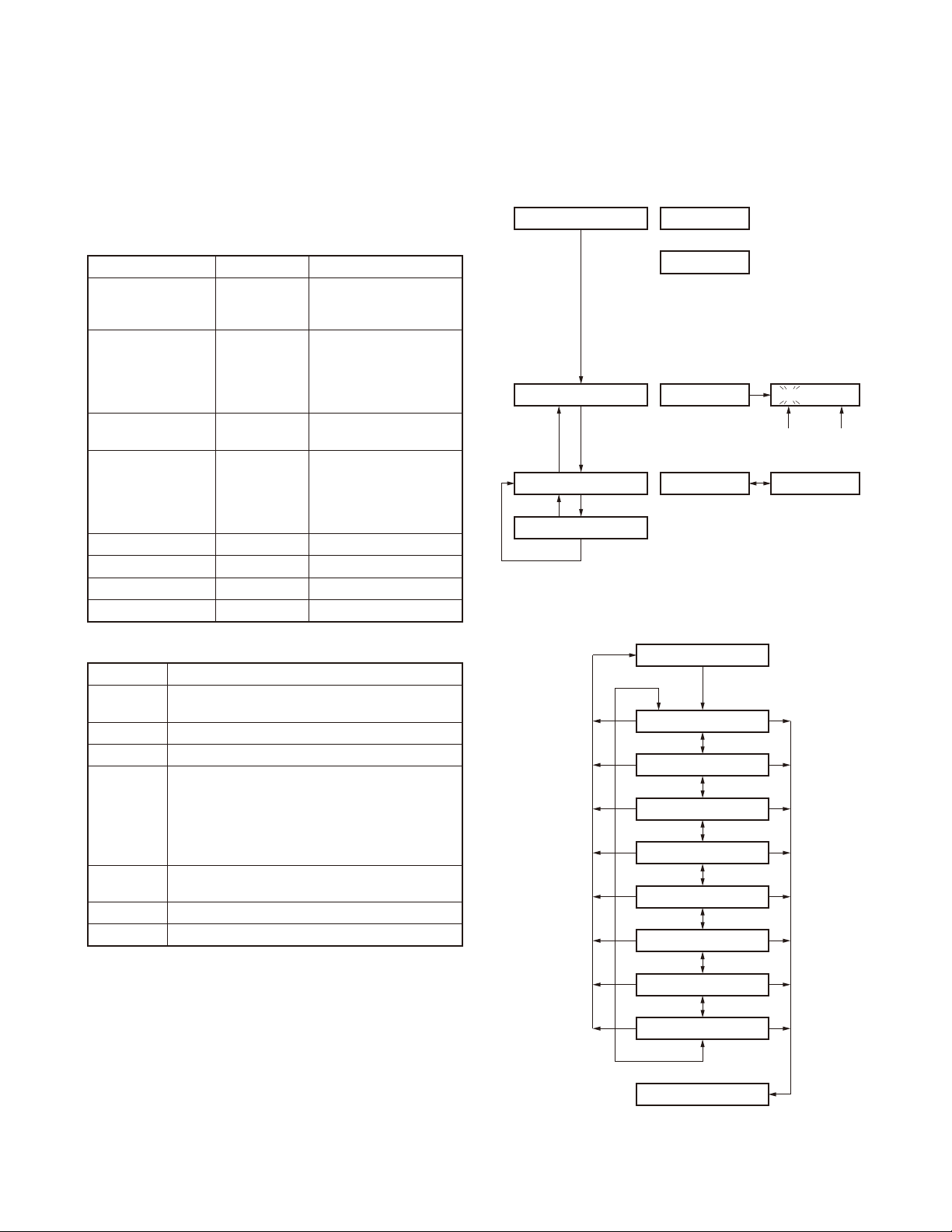
5-6. Self Programming Mode fl ow chart
Channel selection mode fl ow chart
■
[S]+Power ON
Data password
Read authorization password /
Overwrite password entry (6 digits)
[S]
Self programming mode
[S][A]
Channel selection mode
[S][A]
Item setting mode
[S]
Item selection mode fl ow chart
■
Display
SLF.LOCK.R
or
SLF.LOCK.W
SELF
Zone selection
[<B] : Zone/Channel number decrement
[C>] : Zone/Channel number increment
When the Read
authorization password is
set to the transceiver.
When the Overwrite
authorization password is
set to the transceiver.
Zone Channel
[Selector]
Channel selection
I - I
Key operation
Key Key Function
[Selector]
[Side1] No action
[Side2] No action
[S]
[A]
[<B] Toggle/Decrease the blinking value.
[C>] Toggle/Increase the blinking value.
Changing the selection item (RX/TX frequency and
RX/TX signaling only)
• Store the current settings and return to the Item
Selection mode without backup.
• A MHz digit of the frequency blinks. (RX/TX frequency only)
• The icon of the current signaling confi guration
blinks. (RX/TX signaling only)
Abort the current settings and return to the Item
Selection mode without backup.
Channel selection mode
[S]
1. RX frequency
[Selector]
2. RX signaling
[Selector]
3. TX frequency
[Selector]
4. TX signaling
[Selector]
5. RF power Hi / Low
[Selector]
6. Scan Del / Add
[Selector]
7. Beat shift on / off
[Selector]
8. Compander on / off
[Selector]
Item setting mode
[S][A]
[S][A]
[S][A]
[S][A]
[S][A]
[S][A]
[S][A]
[S][A]
7
TK-2317
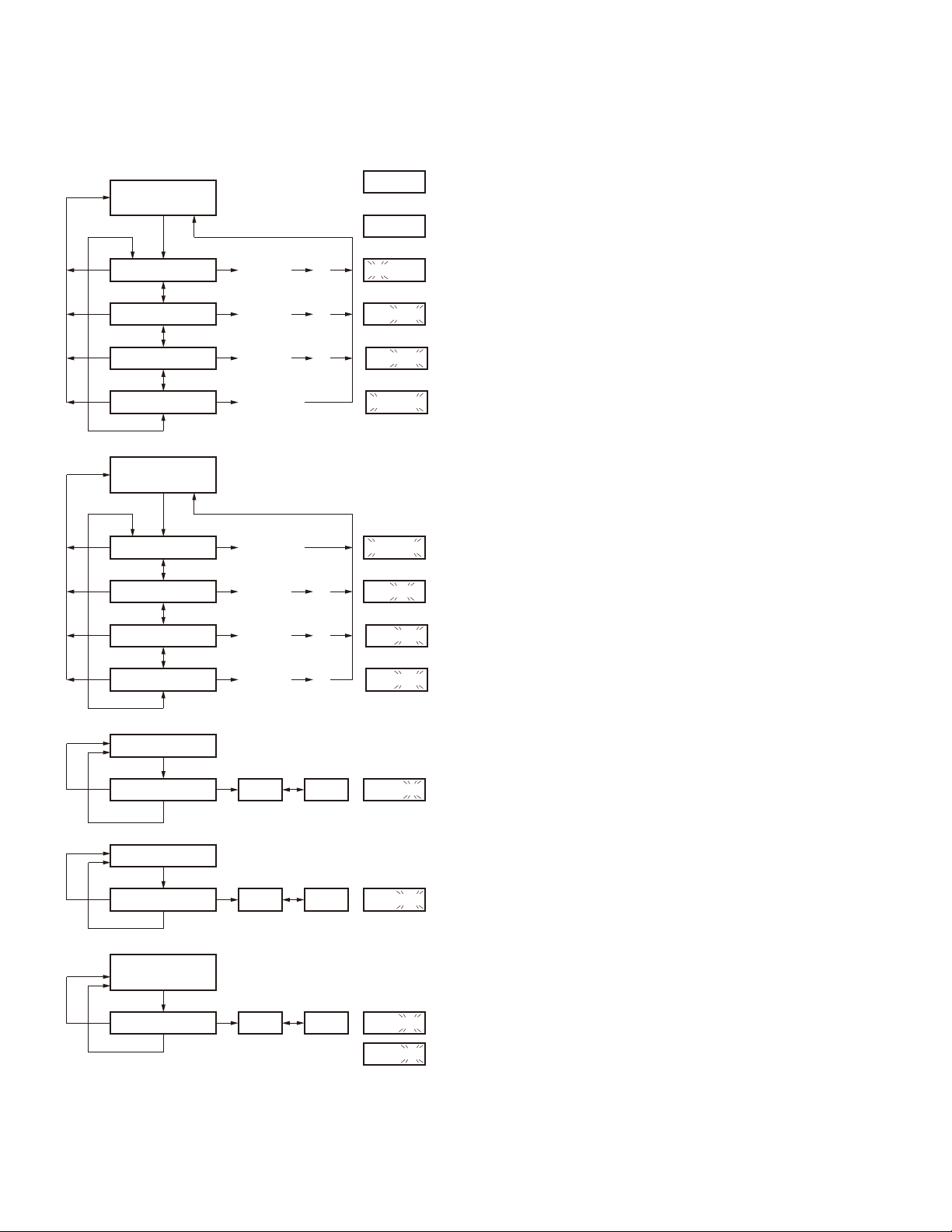
Item setting mode fl ow chart
■
[1. RX frequency] or
[3. TX frequency]
[S]
Current
setting value
Value is not set
REALIGNMENT
6. Firmware Version Information Mode
Display
216. 00000
--------
Tur n the transceiver ON with the [Side1] and [Side2] keys
held down. Then, the version is displayed during holding the
[Side1] and [Side2] keys.
[A]
[A]
[A]
[A]
[2. RX signaling] or
[4. TX signaling]
[A]
[A]
[A]
[A]
MHz setting
[Selector]
kHz setting
[Selector]
Channel step
[Selector]
Frequency clear
[Selector]
[S]
OFF
[Selector]
QT
[Selector]
DQT N
[Selector]
DQT I
[Selector]
[<B] / [C>]
[<B] / [C>]
[<B] / [C>]
[S] : Cleared
[2. RX signaling] or
[4. TX signaling]
OFF
DQT I
[S] : Tone off
[<B] / [C>]
[<B] / [C>]
[S]
[S]
[S]
[S]
[S]
[S][<B] / [C>]
216. 00000
216. 00000
STP 5.00K
--------
Display
TONE OFF
QT 67.0
DQT 023N
DQT 023 I
5. RF power Hi / Low
[A]:
Not
stored
[A]:
Not
stored
[A]:
Not
stored
[S]
Hi / Low selection Hi Low
[S] : Stored
6. Scan Del / Add
[S]
Del / Add selection
[S] : Stored
[7. Beat shift on/off] or
[8. Compander on/off]
[S]
on / off selection on off
[S] : Stored
[<B] / [C>]
[<B] / [C>]
Del Add
[<B] / [C>]
Display
5.PWR HI
Display
6.SCN ADD
Display
7.SFT ON
8.CMP ON
or
8
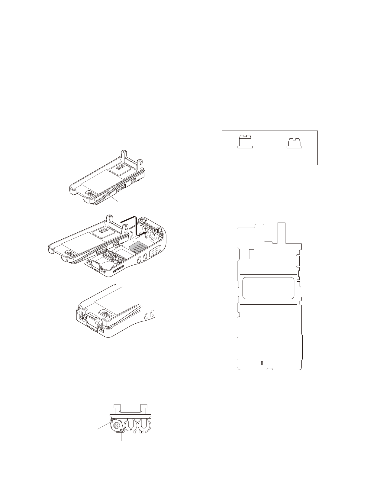
DISASSEMBLY FOR REPAIR
TK-2317
1. Removing the Case Assembly from the Chassis
1. Remove the selector knob a and volume knob b.
2. Remove the two screws c.
3. Lift and remove the chassis from the case assembly
d
(Use a fl at-blade screwdriver to easily lift the chassis.)
b
c
c
d
a
2. Removing the Holder Assembly from the Chassis
1. Remove the holder from the chassis.
Note: Taking care not to cut the speaker and microphone
lead.
2. Detach the solder of speaker and microphone lead from
the PCB beforehand.
3. Remove the packing e from the SP/MIC jack of the TX-
RX unit.
3. Removing the TX-RX unit from the Chassis
1. Remove the eleven screws f fi xing the TX-RX unit.
2. Remove the solder of the antenna terminal with a solder-
.
ing iron g.
3. Remove the solder of the positive terminal with a solder-
ing iron h.
Note: You can remove the TX-RX unit from the chassis
without removing the solder at the positive terminal.
However, in this case, you can not attach the packing
(G53-1605-03) that is on the positive terminal to the
chassis in assembling. So, it is advisable to remove the
solder on the positive terminal fi rst.
4. Remove the FPC from the fl at cable connector i.
5. Lift and remove the TX-RX unit from the chassis j.
g
f
f
f
fx2fx2
j
h
f
fx2
f
i
Note: To remove the Holder Assy from
the Chassis,useaflat-head screwdriver
and insert to this hole.
BLU
YEL
RED
BLK
4. Removing the Battery Release Lever from the Case Assembly
1. Press the upper part of the lever toward the inside of the
case assembly. One side of the shaft will be removed a.
2. Lift and remove the battery release lever from the case
assembly b.
Note: Scratch and widen the glue hole if there is diffi culty
in removing the other end of the shaft.
No glue is required when you reassemble the battery re-
S-
M-
S+
M+
e
lease lever.
b
a
9
TK-2317
DISASSEMBLY FOR REPAIR
5. Attaching the Battery Release Lever to the Case Assembly
1. Insert one side of the shaft into the hole at the lever fi tting
section on the case assembly a.
Caution: The thin spring (G01-4543-14) should be posi-
tioned above the two tabs of the lever.
2. Tilt the battery release lever slightly forward b, so that
the thick spring (G01-4542-04) is positioned below the
case surface.
3. With the thick spring positioned below the case surface,
attach the other side of the shaft to the case assembly
by pressing the battery release lever c until it snaps into
place d.
Caution: Be careful not to tilt the battery release lever
too forward.
If the battery release lever is pushed in this state where
the two tabs come below the case surface, there is a
possibility of damaging the two tabs.
A thin spring
Tow tabs
A thick spring
a
c
Shaft
b
d
6. Assembling the Battery Release Lever
1. Place the lever b onto the stopper a.
2. Place the thick spring c onto the lever.
3. Hook the right and left ends of the thin spr ing d onto the
tabs of the stopper, then place the thin spring onto the
lever e.
4. Slide the shaft through the hole of the stopper and lever f.
d
c
e
b
f
7. Attaching the Positive Terminal to the
Chassis
Always attach the positive terminal to the chassis, using
the following procedures, before mounting the TX-RX unit
onto the chassis.
1. Remove the holder assembly b from the packing a of
the positive terminal.
2. Mount the packing of the positive terminal into the chassis hole c.
3. Mount the holder assembly into the packing of the positive terminal d.
10
b
c
a
d
DISASSEMBLY FOR REPAIR
g
TK-2317
8. Mounting the Chassis to the Case Assembly
1. Confirm that the waterproof packing attached to the
circumference of the chassis is securely inserted in the
groove of the chassis a.
2. Inser t the upper par t of the chassis into the case assembly b.
3. Press the chassis c and the case assembly together to
attach them.
Caution: If the packing of the SP/MIC does not come
to the correct position after attaching the chassis to the
case assembly, reposition the packing with your fi ngers.
a
b
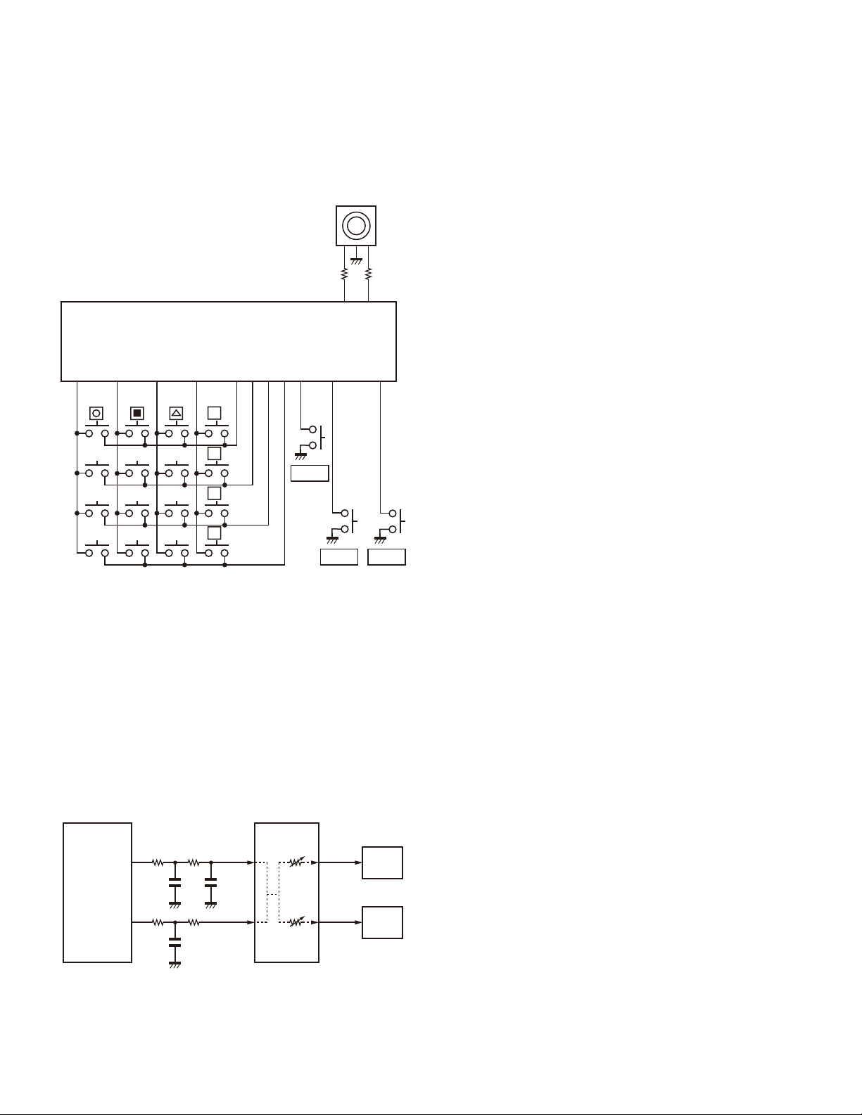
10. The Nuts of the Volume Knob and Channel Knob
Note that the shapes, colors and heights of nuts of the
volume knob and channel knob are different from one
another. (The nut of volume knob is silver, and the nut of
channel knob is gold.)
Use the following jig when removing the nuts of the vol-
ume knob and channel knob.
• Jig (Part No.: W05-1012-00)
for Volume knob
(Long)
for Selector knob
(Short)
11. Screw sequence for mounting the TXRX unit to the chassis
Attach the TX-RX unit to the chassis using the screws in
the order shown in the drawing below.
j
k
9. Attaching the Antenna Receptacle to the Chassis
Screw the antenna receptacle to the chassis in the or-
der shown in the drawing so that the antenna receptacle
comes to the center of the case hole.
TX-RX UNIT
Component side view
i
d
a
eb
fc
gh
Tighten this screw second.
hten this screw first.
Ti
11
TK-2317
CIRCUIT DESCRIPTION
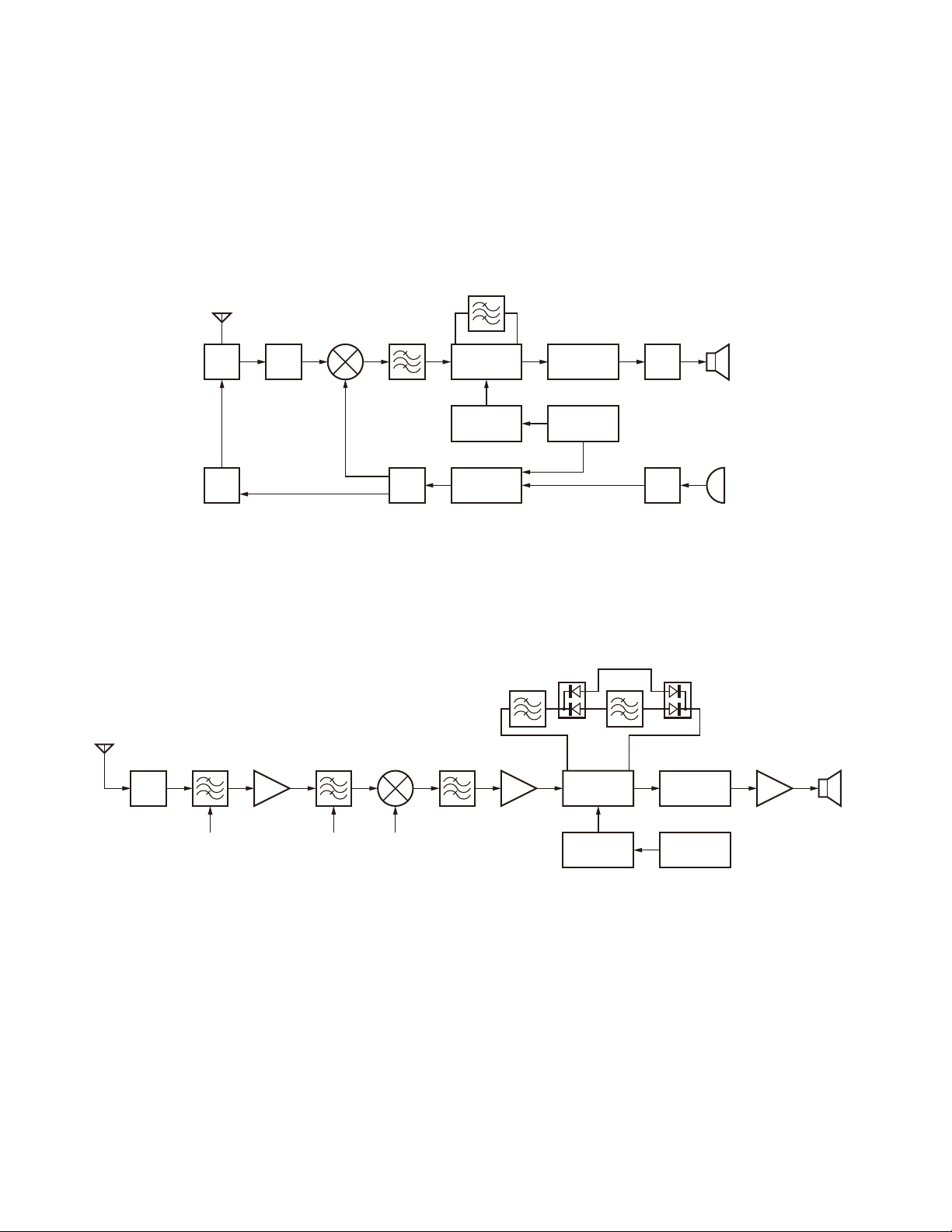
1. Frequency Confi guration
The receiver utilizes double conversion. The first IF is
49.95MHz and the second IF is 450kHz. The fi rst Local oscillator is supplied from the PLL circuit.
The PLL circuit in the transmitter generates the neces-
sary frequencies.
TX/RX: 216~223MHz
ANT
ANT
SW
TX
AMP
RF
AMP
216~223MHz
2. Receiver System
The receiver system is shown in Figure 2.
CF
450kHz
1st MIX MCF SP
AF
AMP
MIC
MIC
AMP
49.95MHz
265.95~
272.95MHz
RF
AMP
IF
System
50.4MHz
X3
multiply
PLL
VCO
AF
baseband
TCXO 16.8MHz
Fig. 1 Frequency confi guration
CF402 CF401
ANT
BPF
ANT
SW
BPF1
Q407
RF AMP XF401
BPF
BPF1 1st Local
Q406
1st MIX
Fig. 2 Receiver system
2-1. Front End (RF Amplifi er) Circuit
The signal coming from the antenna passes through the
transmit / receive switching diode circuit (D201, D202, D203
and D204) and a BPF (L418 and L419), and is then amplifi ed by the RF amplifi er (Q407).
The resulting signal passes through a BPF (L419, L418,
L416 and L414) and goes to the mixer. These BPFs are adjusted by variable capacitance diodes (D408, D407, D405
and D404). The input voltage to the variable capacitance
diodes is a regulated voltage output from the DC amplifi er
(IC811).
12
MCF
Q405
IF AMP
IC401
IF,MIX,DET
Q403
X3 multiply
2nd Local
IC812
AF
baseband
X1
TCXO
16.8MHz
IC815
AF PA
2-2. First Mixer
The signal from the front end is mixed with the fi rst local
oscillator signal generated in the PLL circuit by Q406 to produce a fi rst IF frequency of 49.95MHz.
The resulting signal passes through the XF401 MCF to
cut the adjacent spurious and provide the optimum characteristics, such as adjacent frequency selectivity.
SP
CIRCUIT DESCRIPTION
TK-2317
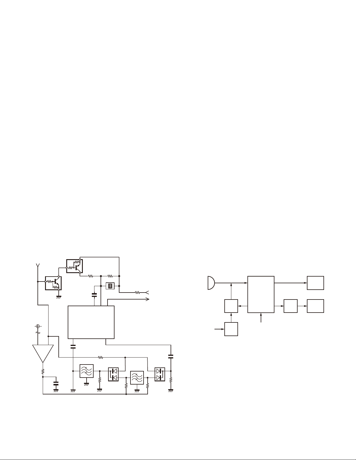
2-3. IF Amplifi er Circuit
The fi rst IF signal is passed through a four-pole monolithic crystal fi lter (XF401) to remove the adjacent channel
signal. The fi ltered fi rst IF signal is amplifi ed by the fi rst IF
amplifier (Q405) and is then applied to the IF system IC
(IC401).
The IF system IC provides a second mixer, limiting
amplifier, quadrature detector and RSSI (Received Signal
Strength Indicator). The second mixer mixes the fi rst IF signal with the 50.4MHz signal of the second local oscillator
output (Q403) and produces the second IF signal of 450kHz.
The second IF signal is passed through the ceramic fi lter (Wide: CF402, Narrow: CF401) to remove the adjacent
channel signal. The fi ltered second IF signal is amplifi ed by
the limiting amplifi er and demodulated by the quadrature detector with the ceramic discriminator (CD401). The demodulated signal is routed to the audio circuit.
2-4. Wide/Narrow Switching Circuit
Wide and narrow settings can be made for each channel
by switching the ceramic fi lters CF401 (narrow).
The second IF signal always passes the ceramic fi lters
CF402 (Wide).
The wide and narrow switching data is output from the
MCU (IC820).
D401 and D402 are switched to ceramic fi lters when a
narrow mode is selected.
Q404 turns on/off with the Narrow and the IC401 detector
output level is changed to maintain a constant output level
during wide or narrow signals.
WID/NAR
Q404
2-5. Audio Amplifi er Circuit
The demodulated signal from IC401 is sent to an AF amplifi er through baseband IC (IC812), and is routed to an audio power amplifi er (IC815) where it is amplifi ed and output
to the speaker.
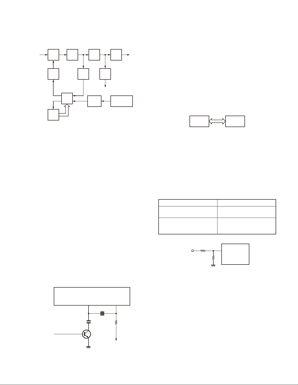
2-6. Squelch Circuit
Part of the AF signal from the IC401 enters the FM system IC (IC401) again, and the noise component is amplifi ed
and rectified by a filter and an amplifier to produce a DC
voltage corresponding to the noise level.
The DC signal from the FM IC goes to the analog port of
the MCU (IC820). IC820 determines whether or not to output
sounds from the speaker by checking if the input voltage is
higher or lower than the preset value.
To output sounds from the speaker, IC820 sends a high
signal to the AF_CONT line and turns IC815 on through
Q813, Q814, Q818 and Q819.
3. T ransmitter System
3-1. Microphone Amplifi er Circuit
The signal from the microphone is limited by the AGC
circuit, which is composed of D807, D808, Q810, Q811 and
the mute switch (Q809). IC812 is composed of a high-pass
fi lter, low-pass fi lter and pre-emphasis/IDC circuit.
The signal from the microphone and the low speed data
from the MCU (IC820) enter the baseband IC (IC812) and
pass through each path and are mixed inside the IC.
The output signal from the baseband IC goes to the VCO
modulation input. The other output signal passes through the
amplifi er (IC3) and goes to the TCXO modulation input.
C424
IFOUT
R409
R424
CD401
QUAD
AFOUT
IFI
D401
R406
Q401
+-
IC402
R471
R423
IC401
MXO
C404
CF402
C402
Fig. 3 Wide/Narrow switching circuit
CF401
R408
R426
50C
AFOUT
D402
R411
C414
R415
MIC
D807,808
Q810,811
MIC_MT
AGC
SW
Q809
IC812
Baseband
IC
LSD
OUT
Fig. 4 Microphone amplifi er circuit
IC3
AMP
VCO
X1
TCXO
13
TK-2317
CIRCUIT DESCRIPTION
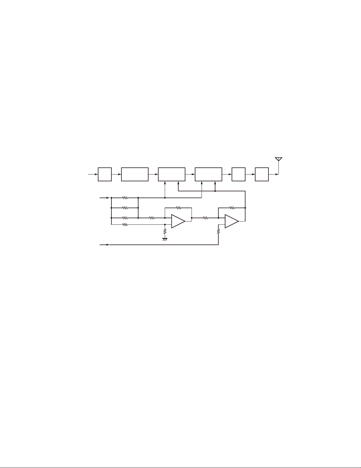
3-2. Drive and Final Amplifi er Circuit
The signal from the T/R switch (D18 is on) is amplifi ed by
the RF AMP (Q201) and pre-drive amplifi er (Q203) to 50mW.
The output of the pre-drive amplifi er is amplifi ed by the
drive amplifi er (Q204) and the RF fi nal amplifi er (Q205) to
5.0W (1W when the power is low).
The drive amplifi er and the RF fi nal amplifi er consist of
two MOS FET stages.
The output of the RF final amplifier is then passed
through the harmonic fi lter (LPF) and antenna switch (D201
and D202) and is applied to the antenna terminal.
From
T/R SW
(D18)
Q201 Q205
RF
AMP
+B
Q203
Pre-DRIVE
AMP
R307
R309
R310
Q204
DRIVE
AMP
VDD
3-3. APC Circuit
The APC circuit always monitors the current flowing
through the drive amplifi er (Q204) and the RF power amplifi er (Q205) and keeps a constant current. The voltage drop
at R307, R309 and R310 is caused by the current fl owing
through the RF fi nal amplifi er. This voltage is applied to the
differential amplifi er IC301 (1/2).
IC301 (2/2) compares the output voltage of IC301 (1/2)
with the reference voltage from IC811. The output of IC301
(2/2) controls the VG of the RF power amplifi er and the drive
amplifi er to make both voltages the same.
The change of power high/low is carried out by the
change of the reference voltage.
ANT
D201,202
RF FINAL
AMP
VG
ANT
SW
LPF
PC/BPF2
(IC811)
Fig. 5 Drive and fi nal amplifi er and APC circuit
4. Frequency Synthesizer Unit
4-1. Frequency synthesizer
The frequency synthesizer consists of the TCXO (X1),
VCO, PLL-IC (IC1), and buffer amplifi ers.
The TCXO generates 16.8MHz. The frequency stability is
1.5ppm within the temperature range of –30°C to +60°C. The
frequency tuning and modulation of the TCXO are done to
apply voltage to pin 1 of the TCXO. The output of the TCXO
is applied to pin 10 of PLL-IC.
The VCO consists of 2 VCO and covers a dual range of
216.00~223.00MHz and 265.95~272.95MHz. The VCO generates 265.95~272.95MHz for providing the fi rst local signal
for reception. The operating frequency is generated by Q5 in
transmitting mode and Q4 in receiving mode. The oscillation
frequency is controlled by applying the VCO control voltage,
obtained from the phase comparator (IC1) to the variable capacitance diodes (D4, D6, D8 and D9 in transmitting mode
and D10 and D12 in receiving mode)
IC301
(1/2)
The TX/RX pin of IC820 goes “high” in transmitting mode,
causing Q7 and Q4 to turn off, and Q5 turn on. The TX/RX
pin goes “low” in receiving mode.
The output from Q4 and Q5 are amplifi ed by a buffer amplifi er (Q8) and Q2, and then sent to the PLL-IC.
The PLL-IC consists of a prescaler, reference divider,
phase comparator, and charge pump. The input signal from
pin 10 and 17 of the PLL-IC is divided down and compared
at the phase comparator. The pulsed output signal of the
phase comparator is applied to the charge pump and transformed into a DC signal in the loop fi lter (LPF). The DC signal is applied to the CV of the VCO and locked to keep the
VCO frequency constant.
PLL data is output from PL_STB (pin 20), PL_CLK (pin 8),
and PL_DAT (pin 21) of the MCU (IC820). The data is input
to the PLL-IC when the channel is changed or transmission
is changed to reception and vice versa. PLL lock condition is
always monitored by pin 18 (PL_UL) of the MCU. When the
PLL is unlocked, PL_UL goes low.
IC301
(2/2)
14
CIRCUIT DESCRIPTION
TK-2317
SWLPF
VC
D18
SW To
RF AMP
Baseband
IC
TX/RX
(TX: High)
PL_UL
Q8
VCO
MCU
IC820
BUFF
CV
IC1
21
7
PL_STB,PL_CLK,PL_DAT
17
PLL
10
Q9
BUFF
D17Q2
RF
AMP
To mixer
TCXO
X1 IC812
Fig. 6 PLL block diagram
5. Control Circuit
The control consists of the MCU (IC820) and its peripheral circuits. It controls the TX-RX unit. IC820 mainly performs
the following;
1) Switching between transmission and reception by PTT
signal input.
2) Reading channel information, frequency, and program
data from the memory circuit.
3) Sending frequency program data to the PLL.
4) Controlling squelch on/off via the DC voltage from the
squelch circuit.
5) Controlling the audio mute circuit via the decode data in-
put.
6) Transmitting tone and encode data.
5-1. Frequency Shift Circuit
The MCU (IC820) and baseband IC (IC812) operates at
a clock frequency of 19.2MHz. The oscillator circuit has the
baseband IC. This oscillator has a circuit that shifts the frequency via Beat shift switch (Q806).
A beat sound may be able to be evaded if “Beat Shift“ is
set to ON when it is generated in the internal spurious transmission modulated sound of the transceiver.
5-2. Memory Circuit
The Memory circuit consists of the MCU (IC820) and
EEPROM (IC810). The EEPROM has a capacity of 512k bits
and stores the channel information, the last channel data,
the scan on status, and other parameters.
EEPROM
■
Note:
The EEPROM stores tuning data (Deviation, Squelch,
etc.).
Realign the transceiver after replacing the EEPROM.
IC820 IC810
MCU
EEPROM
Fig. 8 Memory circuit
5-3. Low Battery Warning
The battery voltage is monitored by the MCU (IC820 pin
63: BATT). When the batter y voltage falls below the voltage
set by the Low Battery Warning adjustment, the red LED
blinks, notifying the operator that it is time to replace the battery (when the always option (default setting) under the Battery Warning function in the FPU is selected). If the battery
voltage falls bellow 5.9V, the transceiver does not transmit
and the warning tone beeps while the PTT switch is pressed.
Low battery warning Battery status
The red LED blinks during
transmission.
The red LED blinks and the
warning tone beeps while the
PTT switch is pressed.
R824
SB
The battery voltage is low but
the transceiver is still usable.
The battery voltage is lowand
the transceiver cannotbe used
to make calls.
63
BATT
IC820
R829
MCU
Fig. 9 Low battery warning
IC812
Baseband IC
XOUT XIN
39 40
X802
MCU
BSHIFT
C846
H: OFF
L: ON
Q806
Fig. 7 Frequency shift circuit
R857
MCU
XIN
15
TK-2317
CIRCUIT DESCRIPTION
5-4. Key Input
Keys and channel selector circuit.
The signal from the keys and channel selector are direct-
ly input to the MCU, as shown in Figure 10.
Selector
KEY1O
KEY2O
KEY3O
IC820
MCU
KEY4O
S
A
B
C
KEY1I
KEY2I
KEY3I
KEY4I
PF2
Side2
PF1
Side1
EN2
EN1
PTT
PTT
Fig. 10 Key input
6. Signaling Circuit
6-1. Encode
Low-speed data (QT, DQT)
■
Low-speed data is output from pin 2 of the MCU. The signal passes through the low pass CR fi lter, and goes to the
baseband IC (IC812). The signal is mixed with the audio signal and goes to the VCO and TCXO (X1) modulation input
after passing through the D/A converter inside the baseband
IC (IC812) for BAL adjustment.
IC820
MCU
LSDO
HSDENC
2
ALT
3
MIC
Fig. 11 Encode
Baseband IC
18
21
IC812
24
MOD2
23
MOD1
VCO
TCXO
High-speed data (2-tone)
■
High-speed data (HSD) is output from pin 3 of the MCU.
HSD deviation made by an adjustment in the MCU is passed
through the low pass CR fi lter and then applied to the baseband (IC812).
The signal is mixed with the audio signal and goes to the
VCO and TCXO.
MSK/DTMF
■
The MSK/DTMF signal is generated in the baseband IC
(IC812). The signal passes through the D/A converter (inside the baseband IC812) and is routed to the VCO. When
encoding the MSK/DTMF, the microphone input signal is
muted.
6-2. Decode
QT/DQT
■
The output signal from the IF IC (IC401) enters the MCU
(IC820) through IC812. IC820 determines whether or not
the QT or DQT matches the preset value, and controls the
AFSW and speaker output sounds according to the squelch
results.
2-tone
■
Part of the received AF signal output from the IF IC (IC401)
passes through the baseband IC (IC812) goes to the other
AF amplifi er IC820 and 816, is compared, and then goes to
IC820. IC820 checks whether or not the 2-tone data is necessary. If it matches, IC820 carries out a specifi ed operation,
such as turning the speaker on.
MSK (Fleet Sync)
■
The MSK input signal from the IF IC (IC401) goes to
IC812. The decoded information is then processed by the
MCU.
DTMF
■
The DTMF input signal from the IF IC (IC401) goes to
IC812. The decoded information is then processed by the
MCU.
7. Power Supply
There are fi ve 5V power supplies and three 3.3V power
supplies: 50M, 50V, 50C, 50R, 50T, 33M, 33MS and 33B.
50M and 33M are always output while the power is on.
33MS is always output, but turns off when the power is
turned off, to prevent malfunction of the MCU.
50C is a common 5V and is output when SAVE is not set
to ON.
50R is 5V for reception and output during reception.
50T is 5V for transmission and output during transmission.
50V is 5V for the SP/MIC connector.
33B is 3.3V for the baseband IC (IC812).
16
 Loading...