

UHF FM TRANSCEIVER
TK-3302/3302(U
TK-3306
SERVICE MANUAL
)
© 2008-9 PRINTED IN JA PAN
B51-8840-00 (N) 672
CONTENTS
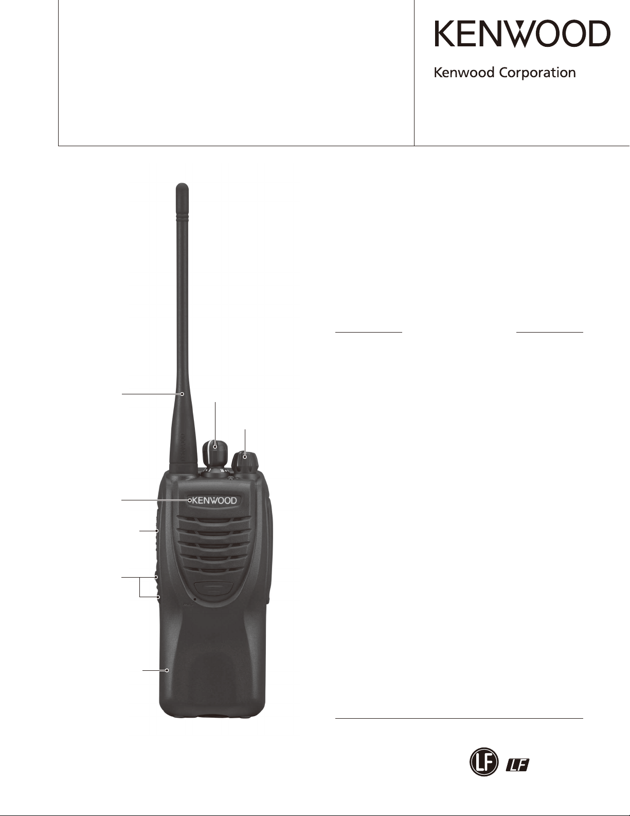
Whip antenna
(T90-1039-25)
(T90-1041-25)
Badge (Front)
(B43-1622-04)
Button knob (PTT)
(K29-9425-03)
Button knob
(Side1/Side2)
(K29-9426-03)
Plastic cabinet assy
(A02-4040-03)
Knob (Selector)
(K29-9427-03)
Knob (Volume)
(K29-9309-13)
GENERAL .....................................................2
SYSTEM SET-UP .........................................3
REALIGNMENT ...........................................3
DISASSEMBLY FOR REPAIR ......................6
CIRCUIT DESCRIPTION ..............................9
SEMICONDUCTOR DATA .........................13
TERMINAL FUNCTION .............................13
COMPONENTS DESCRIPTION .................14
PARTS LIST ...............................................15
EXPLODED VIEW ......................................23
PACKING ....................................................24
ADJUSTMENT ..........................................26
PC BOARD
TX-RX UNIT (X57-7580-XX) ..................32
SCHEMATIC DIAGRAM ............................36
BLOCK DIAGRAM .....................................40
LEVEL DIAGRAM ......................................42
SPECIFICATIONS ......................................43
This product complies with the RoHS directive for the European market.
.
This product uses Lead Free solder.

TK-3302/3302(U)/3306
Document Copyrights
Copyright 2008 by Kenwood Corporation. All rights re-
served.
No part of this manual may be reproduced, translated,
distributed, or transmitted in any form or by any means,
electronic, mechanical, photocopying, recording, or otherwise, for any purpose without the prior written permission
of Kenwood.
GENERAL
INTRODUCTION
SCOPE OF THIS MANUAL
This manual is intended for use by experienced tech ni cians familiar with similar types of commercial grade com mu ni ca tions equipment. It contains all required service
in for ma tion for the equipment and is current as of the publication date. Changes which may occur after publication
are covered by either Service Bulletins or Manual Revisions.
These are is sued as required.
Disclaimer
While every precaution has been taken in the preparation
of this manual, Kenwood assumes no responsibility for errors or omissions. Neither is any liability assumed for damages resulting from the use of the information contained
herein. Kenwood reserves the right to make changes to any
products herein at any time for improvement purposes.
PERSONAL SAFETY
The following precautions are recommended for personal
safety:
• DO NOT transmit until all RF connectors are verifi ed se-
cure and any open connectors are properly terminated.
• SHUT OFF and DO NOT operate this equipment near
elec tri cal blasting caps or in an explosive atmosphere.
• This equipment should be serviced by a qualifi ed tech ni -
cian only.
ORDERING REPLACEMENT PARTS
When ordering replacement parts or equipment in for ma tion, the full part identifi cation number should be in clud ed.
This applies to all parts : components, kits, or chassis. If the
part number is not known, include the chassis or kit number
of which it is a part, and a suffi cient description of the re quired component for proper identifi cation.
SERVICE
This transceiver is designed for easy servicing. Refer to
the sche mat ic diagrams, printed circuit board views, and
align ment procedures contained within.
Model Type TX-RX unit
TK-3302 K,M,P
TK-3302(U) K
TK-3306 M
TK-3306 M3 X57-7580-23 400~430MHz
X57-7580-20 450~490MHz
Frequency range
Remarks
IF1:
38.85MHz
LOC:
38.4MHz
2
SYSTEM SET-UP
TK-3302/3302(U)/3306
Merchandise received
Choose the type of transceiver
Transceiver programming
Are you using the optional antenna?
NO
Are you using the speaker microphone?
NO
Delivery
Frequency range (MHz) RF power Type
TX/RX 450~490
TX/RX 400~430
A personal computer, programming interface (KPG-22/22A),
and FPU (programming software) are required for programming.
(The frequency, TX power HI/LOW, and signalling data are
programmed for the transceiver.)
YES
YES
KRA-23 or KRA-27
Optional antenna
KMC-17, KMC-21 or KMC-45
Speaker microphone
4.0W
4.0W
(Option)
TK-3302: K,M,P
TK-3302(U): K
TK-3306: M
TK-3306: M3
1. Modes
User mode
PC mode
Wireless clone mode
Mode Function
User mode For normal use.
PC mode
Data programming
mode
PC test mode
Wireless clone
mode
Used for communication between the transceiver and PC.
Used to read and write frequency data and
other features to and from the transceiver.
Used to check the transceiver using the PC.
This feature is included in the FPU.
Used to transfer programming data from
one transceiver to another.
PC test mode
REALIGNMENT
Data programming mode
PC tuning mode
2. How to Enter Each Mode
Mode Operation
User mode Power ON
PC mode Received commands from PC
Wireless clone mode [PTT]+[Side2]+Power ON (Two seconds)
3. PC Mode
3-1. Preface
The transceiver is programmed by using a personal computer, a programming interface (KPG-22/22A, USB adapter
(KCT-53U)) and FPU (programming software).
The programming software can be used with a PC or
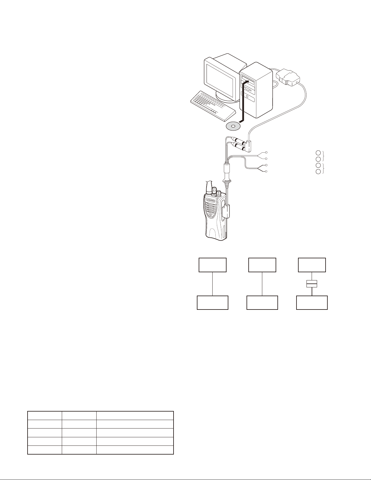
compatible. Figure 1 shows the setup of a PC for programming.
3-2. Connection Procedure
1. Connect the transceiver to the personal computer with
the interface cable and USB adapter (when the interface
cable is KPG-22A, the KCT-53U can be used).
3
TK-3302/3302(U)/3306
REALIGNMENT
Notes:
• You must install the KCT-53U driver in the computer to
use the USB adapter (KCT-53U).
• When using the USB adapter (KCT-53U) for the fi rst time,
plug the KCT-53U into a USB port on the computer with
the computer power ON.
2. When the POWER is switched on, user mode can be entered immediately. When the PC sends a command, the
transceiver enters PC mode.
When data is read from the transceiver, the red LED
lights.
When data is written to by the transceiver, the green LED
lights.
Notes :
• The data stored in the personal computer must match
Model Name and Model Type when it is written into EEPROM.
• Do not press the [PTT] key during data transmission or
reception.
3-3. KPG-22/KPG-22A Description
(PC programming interface cable : Option)
The KPG-22/22A is required to interface the transceiver
with the computer. It has a circuit in its D-sub connector
(KPG-22: 25-pin, KPG-22A: 9-pin) case that converts the RS232C logic level to the TTL level.
The KPG-22/22A connects the SP/MIC connector of the
transceiver to the RS-232C serial port of the computer.
3-4. KCT-53U Description (USB adapter : Option)
The KCT-53U is a cable which connects the KPG-22A to a
USB port on a computer.
When using the KCT-53U, install the supplied CD-ROM
(with driver software) in the computer. The KCT-53U driver
runs under Windows 2000 or XP.
3-5. FPU (Programming Software) Description
The FPU is the programming software for the transceiver
supplied on a CD-ROM. The software on this disk allows a
user to program the transceiver transceivers via Programming interface cable (KPG-22/22A).
PC
FPU
Tuning cable
(E30-3216-05)
PC
D-SUB
(25-pin)
KPG-22
Transceiver Transceiver Transceiver
D-SUB
(9-pin)
KPG-22 or KPG-22A or
KPG-22A+KCT-53U
Illustration is KPG-22
Gray
Gray/Black
1.5D-XV Lead wire
1.5D-XV Shield wire
PC
KPG-22A
+
–
+
–
PC
USB
KCT-53U
KPG-22A
Fig. 1
SP
MIC
3-6. Programming with PC
If data is transferred to the transceiver from a PC with the
FPU, the data for each set can be modifi ed.
Data can be programmed into the EEPROM in RS-232C
format via the SP/MIC jack.
In this mode the PTT line operate as TXD and RXD data
lines respectively.
List of FPU for transceiver
Model Type FPU
TK-3302 K,M KPG-118D(K)
TK-3302 P KPG-119D(K)
TK-3302(U) K KPG-119D(K)
TK-3306 M,M3 KPG-118D(M)
4
4. Wireless Clone Mode
4-1. Outline
“Wireless Clone Mode” copies the transceiver data to
another transceiver.
The dealer can copy the transceiver data to another trans-
ceiver even without the use of a personal computer.
4-2. Example
The transceiver can copy the programming data to one or
more transceivers via RF communication.
The clone source and clone target/s must be in wireless
clone mode.

REALIGNMENT
TK-3302/3302(U)/3306
4-3. Operation
1. To switch the clone target/s to wireless clone mode,
press and hold the [PTT] and [side2] keys while turning
the transceiver power ON.
2. Wait for 2 seconds. The LED will light orange and the
transceiver will announce “Clone”.
3. Select a channel table number using Side1 (increment
channel table) and Side2 (decrement channnel table)
keys.
4. To switch the clone source to wireless clone mode, press
and hold the [PTT] and [side2] keys while turning the
transceiver power ON.
5. Wait for 2 seconds. The LED will light orange and the
transceiver will announce “Clone”.
6. Select the same channel table number as the clone
target/s.
7. Press [PTT] on the clone source to begin data transmission.
When the clone target starts to receive data, the LED will
light green.
When the clone source fi nishes sending data, a “confi r-
mation” tone will sound.
If data transmission fails while cloning, an “error” tone
will sound from the target unit.
8. If the cloning fails, no data will be available in the target
unit when it is returned to User mode.
9. When the cloning is successful, the target unit’s “Scan”
and “Key lock” functions will return to their default values
(Scan = OFF, Key lock = OFF).
Notes:
• The dealer can clone data to two or more transceivers by
repeating the above procedures.
• If the transceivers wireless clone mode is confi gured as
“Disabled”, the transceiver cannot enter wireless clone
mode.
• The table shown below will cover the frequency tables
used for wireless cloning.
• Wireless clone mode cannot be entered in battery low
state.
• A unit cannot be a “Source Unit” if it is unprogrammed. If
[PTT] is pressed, an “error” tone will sound.
• The language used in cloning depends on the “Model
type” setting, not the FPU setting.
• Once a unit is set to be the source, it cannot be a target
after the data has been transmitted. This protects the
data in the source unit.
• Electronic interface may cause a failure in data transfer
during wireless clone, such as when waveforms or electromagnetics are being performed at the workbench.
• Wireless clone mode can be used ONLY by the autho-
rized service personnel.
• The wireless clone mode setting must be confi gured
as “Disable” before being delivered to the end-user.
• To clone, replace the antenna from both the source
transceiver and the target transceiver with a dummy
load.
• The transmit output power is automatically set to
Low in wireless clone mode.
• Clone frequency table
TK-3302 K,M,P
No.
1 450.000 400.000
2 452.000 401.000
3 454.000 402.000
4 456.000 403.000
5 458.000 404.000
6 460.000 405.000
7 462.000 406.000
8 464.000 407.000
9 466.000 408.000
10 468.000 409.000
11 470.000 410.000
12 472.000 411.000
13 474.000 412.000
14 476.000 413.000
15 478.000 414.000
16 480.000 415.000
17 482.000 416.000
18 484.000 417.000
19 486.000 418.000
20 488.000 419.000
TK-3302(U) K
TK-3306 M
450~490 400~430
Operating frequency (MHz)
TK-3306 M3
5
TK-3302/3302(U)/3306
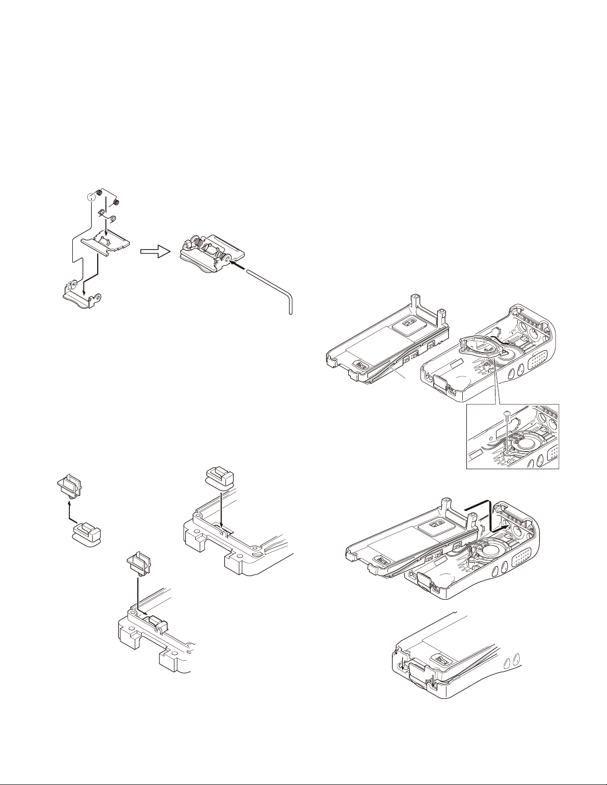
DISASSEMBLY FOR REPAIR
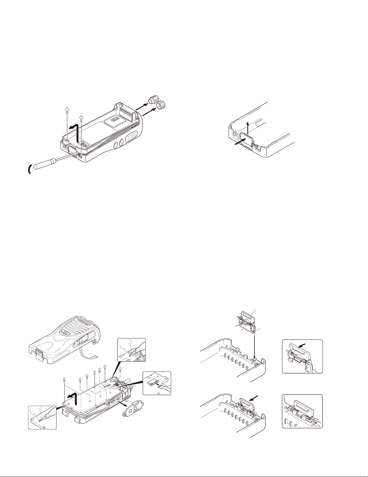
1.
Removing the Case Assembly from the Chassis
1. Remove the volume knob q and channel knob w.
2. Remove the two screws e.
3. Lift and remove the chassis from the case assembly r.
(Use a fl at-blade screwdriver to easily lift the chassis.)
.
.
;
3. Removing the Battery Release Lever
from the Case Assembly
1. Press the upper part of the lever toward the inside of the
case assembly. One side of the shaft will be removed q.
@
:
2. Lift and remove the battery release lever from the case
assembly w.
@
:
4. Attaching the Battery Release Lever to
2.
Removing the TX-RX unit from the Chassis
1. Detach the solder of speaker wire from the PCB beforehand.
2. Remove the packing t from the SP/MIC jack of the TXRX unit.
3. Remove the ten screws y fi xing the TX-RX unit.
4. Remove the solder of the antenna terminal with a soldering iron u.
5. Remove the solder of the positive terminal with a soldering iron i.
Note: You can remove the TX-RX unit from the chas-
sis without removing the solder at the positive terminal.
However, in this case, you can not attach the packing
(G53-1605-03) that is on the positive terminal to the chassis in assembling. So, it is advisable to remove the solder
on the positive terminal fi rst.
6. Remove the FPC from the fl at cable connector o.
7. Lift and remove the TX-RX unit from the chassis !0.
>
the Case Assembly
1. Insert one side of the shaft into the hole at the lever fi tting section on the case assembly q.
Caution: The thin spring (G01-4543-04) should be posi-
tioned above the two tabs of the lever.
2. Tilt the battery release lever slightly forward w, so that
the thick spring (G01-4542-04) is positioned below the
case surface.
3. With the thick spring positioned below the case surface,
attach the other side of the shaft to the case assembly
by pressing the battery release lever e until it snaps into
place r.
Caution: Be careful not to tilt the battery release lever
too forward.
If the battery release lever is pushed in this state where
the two tabs come below the case surface, there is a
possibility of damaging the two tabs.
A thin spring
:
Shaft
@
Tow tabs
A thick spring
B
B
B
B
2
B
B
B
8
=
.
;
6
TK-3302/3302(U)/3306
DISASSEMBLY FOR REPAIR
5. Assembling the Battery Release Lever
1. Place the lever w onto the stopper q.
2. Place the thick spring e onto the lever.
3. Hook the right and left ends of the thin spring r onto the
tabs of the stopper, then place the thin spring onto the
lever t.
4. Slide the shaft through the hole of the stopper and lever
.
y
;
.
=
:
6.
Attaching the Positive Terminal to the Chassis
Always attach the positive terminal to the chassis, using
the following procedures, before mounting the TX-RX unit
onto the chassis.
1. Remove the holder assembly w from the packing q of
the positive terminal.
2. Mount the packing of the positive terminal into the chassis hole e.
3. Mount the holder assembly into the packing of the positive terminal r.
@
B
7.
Mounting the Chassis to the Case Assembly
1. Confirm that the waterproof packing attached to the
circumference of the chassis is securely inserted in the
groove of the chassis q.
2. Attach the speaker with waterproof packing to the
speaker recess of the case assembly w. Make sure the
speaker clasp is securely inserted.
3. Tighten the speaker clasp into the case assembly with
the screw.
4. Insert the upper part of the chassis into the case assembly e.
Caution: Take care that the speaker lead wire is not
caught by the microphone element.
5. Press the chassis r and the case assembly together to
attach them.
Caution: If the packing of the SP/MIC does not come
to the correct position after attaching the chassis to the
case assembly, reposition the packing with your fi ngers.
@
:
Confirm that the
waterproof packing is
securely inserted in the
groove of the chassis.
@
.
.
:
;
;
;
7
TK-3302/3302(U)/3306
DISASSEMBLY FOR REPAIR
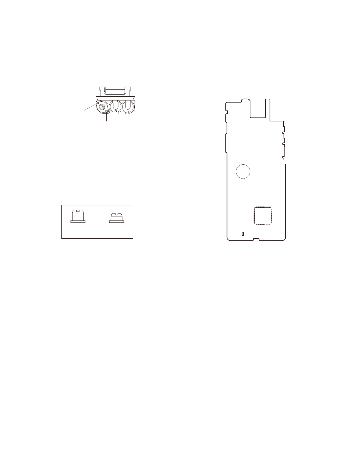
8.
Attaching the Antenna Receptacle to the Chassis
Screw the antenna receptacle to the chassis in the order
shown in the drawing so that the antenna receptacle
comes to the center of the case hole.
10. Screw sequence for mounting the TX-
RX unit to the chassis
Attach the TX-RX unit to the chassis using the screws in
the order shown in the drawing below.
Note: From screw r onward no sequence is need.
;
Tighten this screw first.
Tighten this screw second
9.
The Nuts of the Volume Knob and Channel Knob
Note that the shapes, colors and heights of nuts of the
volume knob and channel knob are different from one
another. (The nut of volume knob is silver, and the nut of
channel knob is gold)
Use the following jig when removing the nuts of the vol-
ume knob and channel knob.
• Jig (Part No.: W05-1012-00)
Volume knob
(Long)
Channel knob
(Short)
;
;
TX-RX UNIT
Component side view
;
:
;;
;
.@
8
TK-3302/3302(U)/3306
CIRCUIT DESCRIPTION
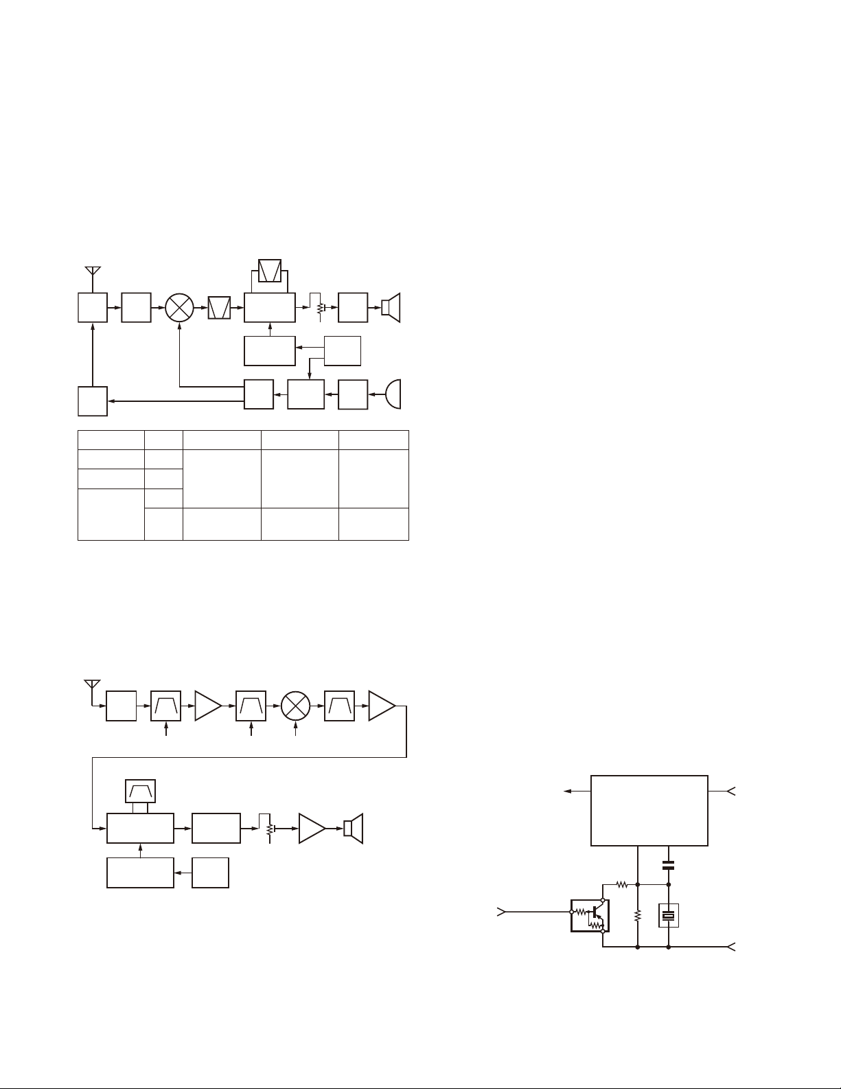
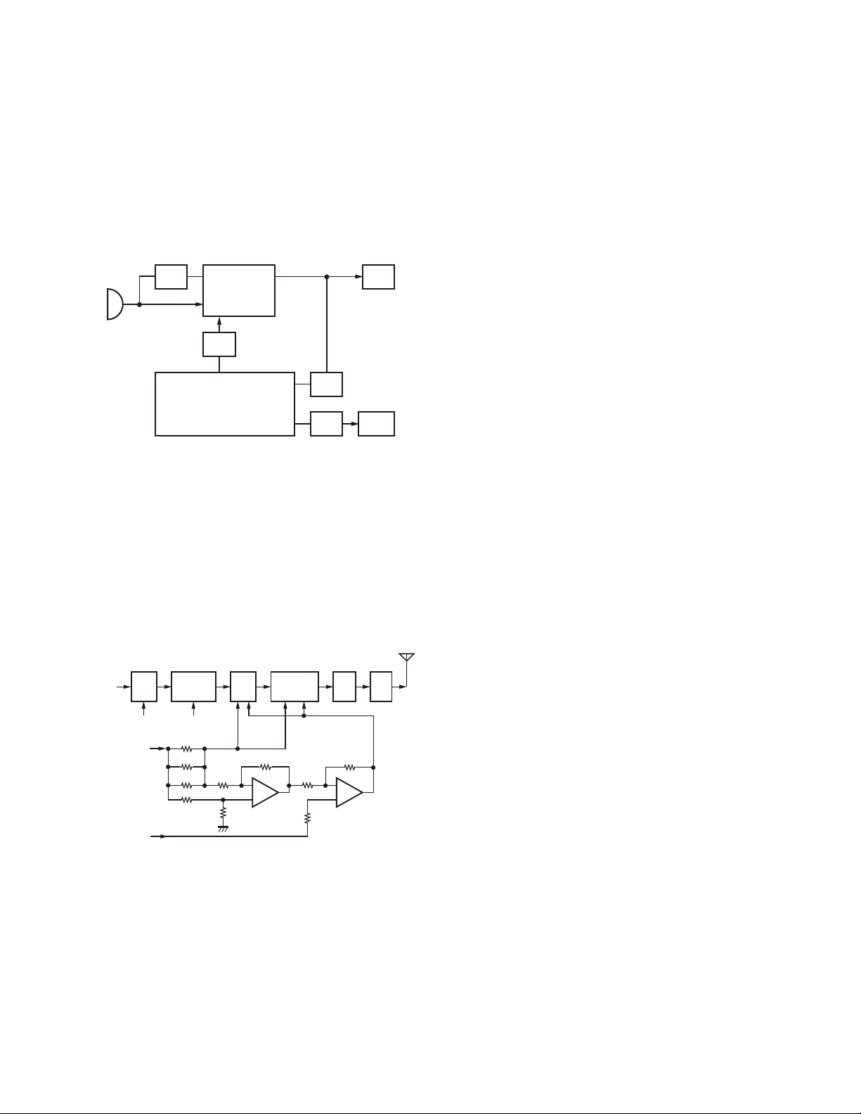
1. Frequency Confi guration
The receiver utilizes double conversion. The first IF is
38.85MHz and the second IF is 450kHz. The fi rst local oscillator signal is supplied from the PLL circuit.
The PLL circuit in the transmitter generates the neces-
sary frequencies. Fig. 1 shows the frequencies.
TX/RX : :
ANT
ANT
SW
TX
AMP
TK-3302(U) K
RF
AMP
Model Type
TK-3302 K,M,P
TK-3306
1st MIX
M
M3 400~430MHz 400~430MHz
MCF
38.85MHz
RX: .
TX: @
qwe
450~490MHz 450~490MHz
CF
450kHz
IF
SYSTEM
38.4MHz
X3
multiply
RF
AMP
PLL
VCO
AF
AMP
TCXO
MIC
AMP
411.15~
451.15MHz
361.15~
391.15MHz
SP
12.8MHz
MIC
Fig. 1 Frequency confi guration
2. Receiver
The frequency confi guration of the receiver is shown in
Fig. 2.
ANT
ANT
SW
BPF
RCTV
RF AMP
Q204
BPF
PCTV
MIXER
Q203
1st Local
MCF
XF201
IF AMP
Q202
fi ed by the RF amplifi er (Q204).
The resulting signal passes through a BPF (L209, L207
and L206) and goes to the mixer. These BPFs are adjusted
by variable capacitors (D201, D202, D203, D204 and D205).
The input voltage to the variable capacitor is regulated by
voltage output from the MCU (IC306).
First Mixer
■
The signal from the front end is mixed with the fi rst local
oscillator signal generated in the PLL circuit by Q203 to produce a fi rst IF frequency of 38.85MHz.
The resulting signal passes through the XF201 MCF to
cut the adjacent spurious and provide the opitimun characteristics, such as adjacent frequency selectivity.
IF Amplifi er Circuit
■
The fi rst IF signal is passed through a four-pole monolithic
crystal fi lter (XF201) to remove the adjacent channel signal.
The fi ltered fi rst IF signal is amplifi ed by the fi rst IF amplifier (Q202) and then applied to the lF system IC (IC201).
The IF system IC provides a second mixer, limiting amplifi er,
quadrature detector and RSSI (Received Signal Strength Indicator). The second mixer mixes the fi rst IF signal with the
38.4MHz of the second local oscillator output (TCXO X1 and
Q2) and produces the second IF signal of 450kHz.
The second IF signal is passed through the ceramic fi lter
(CF201) to remove the adjacent channel signal. The fi ltered
second IF signal is amplified by the limiting amplifier and
demodulated by the quadrature detector with the ceramic
discriminator (CD201). The demodulated signal is routed to
the audio circuit.
Wide/Narrow Switching Circuit
■
Narrow and Wide settings can be made for each channel
by switching the demodulation level.
The WIDE (low level) and NARROW (high level) data is
output from IC306, pin 5. When a WIDE (low level) data is
received, Q201 turn on. When a NARROW (high level) data
is received, Q201 turn off.
Q201 turns on/off with the Wide/Narrow data and the
IC201 detector output level is switched to maintain a constant output level during wide or narrow signals.
CF201
IC201
IF, MIX, DET
Q2
X3 multiplyX1TXCO
2nd Local 12.8MHz
IC308
AQUA-L
AF VOL
IC309
AF PA
SP
Fig. 2 Receiver section
Front End (RF AMP)
■
The signal coming from the antenna passes through the
transmit/receive switching diode circuit, (D103, D104 and
D105) passes through a BPF (L213 and L212), and is ampli-
AFOUT
IC201
FM IF SYSTEM
QUAD IFOUT
W/N
(IC306)
R209
Q201
L : Wide
H: Narrow
C209
R210
Fig. 3 Wide/Narrow switching circuit
Q202
CD201
5R
9
TK-3302/3302(U)/3306
CIRCUIT DESCRIPTION
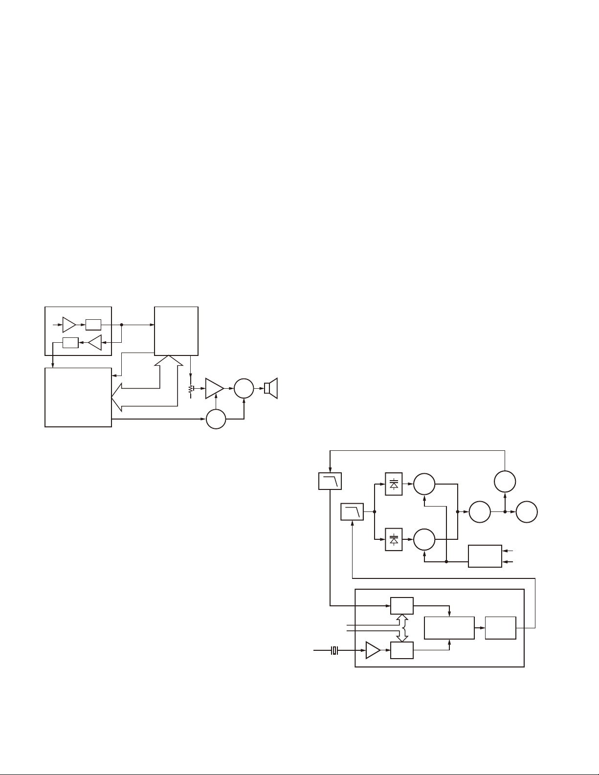
Audio Amplifi er Circuit
■
The demodulated signal from IC201 goes to AF amplifi er
through IC308.
The signal then goes through an AF volume control , and
is routed to an audio power amplifi er (IC309) where it is amplifi ed and output to the speaker.
Squelch
■
Part of the AF signal from the IC enters the FM IC (IC201)
again, and the noise component is amplifi ed and rectifi ed by
a fi lter and an amplifi er to produce a DC voltage corresponding to the noise level.
The DC signal from the FM IC goes to the analog port
of the MCU (IC306). IC306 determines whether to output
sounds from the speaker by checking whether the input
voltage is higher or lower than the preset value.
To output sounds from the speaker, IC306 sends a high
signal to the AF_CONT line and turns IC309 on through
Q312, Q313, Q314, Q315 and Q316. (See Fig. 4)
IC201: FM IF
IF amp
BUSY
QT/DQT IN
IC306
MCU
AF_CONT
SIGNAL
DTMF
QT/DQT
CLK, DATA,
STD, LOADN
IC308
AQUA-L
IC309
AF PA
Q315,316
SW
Q312,313,314
SW
SP
3. PLL Frequency Synthesizer
The PLL circuit generates the fi rst local oscillator signal
for reception and the RF signal for transmission.
PLL
■
The frequency step of the PLL circuit is 5 or 6.25kHz.
A 12.8MHz reference oscillator signal is divided at IC1 by
a fi xed counter to produce an oscillator (VCO) output signal
which is buffer amplifi ed by Q3 then divided in IC1 by a programmable counter. The divided signal is compared in phase
with the 5 or 6.25kHz reference signal from the phase comparator in IC1. The output signal from the phase comparator
is fi ltered through a low-pass fi lter and passed to the VCO
to control the oscillator frequency. (See Fig. 5)
VCO
■
The operating frequency is generated by Q5 in transmit
mode and Q4 in receive mode. The oscillator frequency is
controlled by applying the VCO control voltage, obtained
from the phase comparator, to the varactor diodes (D4 and
D8 in transmit mode and D3 and D6 in receive mode).
The RX_SW pin is set high in receive mode causing Q7
turn on. The TX_SW pin is set high in transmit mode. The
outputs from Q4 and Q5 are amplifi ed by Q9 and sent to the
RF amplifi ers.
Unlock Detector
■
If a pulse signal appears at the LD pin of IC1, an unlock
condition occurs, and the DC voltage obtained from C4 and
Q1 causes the voltage applied to the MCU to go low. When
the MCU detects this condition, the transmitter is disabled,
ignoring the push-to-talk switch input signal.
Fig. 4 AF amplifi er and squelch
Receive Signaling
■
• QT/DQT
The output signal from FM IC (IC201) enters the MCU
(IC306) through IC308. IC306 determines whether the QT or
DQT matches the preset value, and controls the SP MUTE
and the speaker output sounds according to the squelch results.
• MSK (Fleet Sync)
The MSK input signal from the FM IC goes to pin 31 of IC
308. The signal is demodulated by MSK demodulator in IC
308. The demodulated data goes to the MCU for processing.
• DTMF
The DTMF input signal from the FM IC (IC201) goes to
IC308. The decoded information is then processed by the
MCU.
LPF
PLL DATA
X1
12.8MHz
LPF
REF OSC
D4,8Q5TX VCO
D3,6Q4RX VCO
5 or 6.25kHz
1/N
Phase
comparator
1/M
5 or 6.25kHz
Fig. 5 PLL circuit
Q9
BUFF AMP
Q7,8
T/R SW
Charge
pump
Q3
BUFFER
Q11
RF AMP
RX
TX
IC1
PLL IC
10
TK-3302/3302(U)/3306
CIRCUIT DESCRIPTION
4. Transmitter System
Microphone Amplifi er
■
The signal from the microphone passes through the
IC308. When encoding DTMF, it is turned OFF for muting
the microphone input signal by IC308.
The signal passes through the Audio processor (IC308)
for the maximum deviation adjustment, and goes to the
VCO modulation input.
MIC
AGC
IC306
MCU
AQUA-L
LPF
DTMF
IC308
QTVCO
QTTCXO
LPF
LPF TCXO
Fig. 6 Microphone amplifi er
Drive and Final Amplifi er
■
The signal from the T/R switch (D10 is on) is amplifi ed by
the pre-drive (Q101 and Q102) and the drive amplifi er (Q103)
to 500mW.
The output of the drive amplifi er is amplifi ed by the RF
power amplifier (Q106) to 4.0W (1W when the power is
low). The output of the RF power amplifi er is then passed
through the harmonic fi lter (LPF) and antenna switch (D103)
and applied to the antenna terminal.
From
T/R SW
(D10)
RF
AMP
+B
PCTV
(IC306)
Q102Q101 Q103
Pre-drive
AMP
VD
5T5T
R120
R123
R126
Drive
AMP
VG
VDD
Q106
RF power
AMP
VG
IC101
(1/2)
Fig. 7 Drive and fi nal amplifi er and APC circuit
APC Circuit
■
The APC circuit always monitors the current flowing
through the drive amplifi er and RF power amplifi er (Q103
and Q106) and keeps a constant current.
The voltage drop at R120, R123 and R126 is caused by
the current flowing through the RF power amplifier and
drive amplifi er, and this voltage is applied to the differential
amplifi er IC101 (1/2).
D103
ANT
SW
VCO
X1
ANT
LPF
IC101
(2/2)
IC101 (2/2) compares the output voltage of IC101 (1/2)
with the reference voltage from IC306. The output of IC101
(2/2) controls the VG of the RF power amplifier and drive
amplifi er to make both voltages the same.
The change of power high/low is carried out by the
change of the reference voltage.
Encode Signaling
■
• QT/DQT
QT/DQT data of the QTTCXO Line is output from pin 14
of the MCU. The signal passes through a low-pass CR fi lter
and goes to the TCXO (X1).
The QT/DQT data of the QTVCO Line is output from pin
15 of the MCU. The signal passes through a low pass CR fi lter, mixes with the audio signal, and goes to the VCO modulation input. TX deviation is adjusted by the MCU.
• DTMF
High-speed data is output from pin 74 of the MCU. The
signal passes through a low-pass CR fi lter, and provides a
TX and SP out tone, and is then applied to the audio processor (IC308). The signal is mixed with the audio signal and
goes to the VCO.
TX deviation is adjusted by the MCU.
• MSK (Fleet Sync)
Fleet Sync utilizes 1200bps and 2400bps MSK signal is
output from pin 6 of IC308. And is routed to the VCO. When
encoding MSK, the microphone input signal is muted.
5. Power Supply
There are four 5V power supplies in the transceiver: 5M,
5C, 5R, and 5T. 5M for MCU is always output while the
power is on. 5M is always output, but turns off when the
power is turned off to prevent malfunction of the MCU.
5C is a common 5V and is output when SAVE is not set
to OFF.
5R is 5V for reception and output during reception.
5T is 5V for transmission and output during transmission.
6. Control Circuit
The control circuit consists of a MCU (IC306) and its
peripheral circuits. It controls the TX-RX unit. IC306 mainly
performs the following:
1) Switching between transmission and reception by the
PTT signal input.
2) Reading system, group, frequency, and program data
from the memory circuit.
3) Sending frequency program data to the PLL.
4) Controlling squelch on/off by the DC voltage from the
squelch circuit.
5) Controlling the audio mute circuit by the decode data in-
put.
6) Transmitting tone and encode data.
11
TK-3302/3302(U)/3306
CIRCUIT DESCRIPTION
Frequency Shift Circuit
■
The MCU (IC306) operates at a clock of 14.746 MHz. This
oscillator has a circuit that shifts the frequency by BEAT
SHIFT SW (Q305, Q306).
A beat sound may be able to be evaded from generation
if “Beat Shift” is set to ON when it is generated in the internal spurious transmission modulated sound of a transceiver.
SB
R301
R305
66
IC306
MCU
Fig. 10 Low battery warning
IC306
MCU
XOUT XIN
X301
Hi: ON
Q305
Low: OFF
BSHIFT
Q306
Fig. 8 Frequency shift circuit
Memory Circuit
■
Memory circuit consists of the MCU (IC306) and an EEPROM (IC305). An EEPROM has a capacity of 16k bits that
contains the transceiver control program for the MCU and
data such as transceiver channels and operating features.
IC306 IC305
MCU
EEPROM
Fig. 9 Memory circuit
Low Battery Warning
■
The battery voltage is checked using by the MCU. The
transceiver generates a warning tone when it falls below
the warning voltage shown in the table.
1) The red LED blinks when the battery voltage falls below
the voltage (1) shown in the table during transmission.
Note: The transceiver checks the battery voltage during
reception even when, in the FPU, the Battery Warning
status function is set to “On TX” (default setting).
However, the LED does not blink during reception. Dur-
ing transmission, the LED blinks to generate the warning
tone of a low battery voltage.
2) The transceiver immediately stops transmission when
the battery voltage falls below the voltage (2) shown in
the table. A message tone beeps while the PTT switch is
released.
Ni-Cd Battery Ni-MH Battery Li-ion Battery
(1) 6.2V 6.2V 6.2V
(2) 5.9V 5.9V 5.9V
7. Control System
Keys and channel selector circuit. The signal from the
keys and channel selector are directly input to the MCU, as
shown in Fig. 11.
Channel
selector
55
PTT
62
61
60
59
58
EN1
EN2
EN3
EN4
EN5
IC306
MCU
SIDE1
SIDE2
56
57
Fig. 11 Control system
PTT
SW
SW1
SW2
12
SEMICONDUCTOR DATA
MCU: R5F212CCKCMB (TX-RX unit IC306)
Pin No. Signal Name I/O Function
1 5T_C O 5T control
2 PLL_STB O PLL strobe
3 5C_C O 5C control
4 5R_C O 5R control
5 W/N O Wide/Narrow switch
6 MODE I No function
7 AF_CONT O Speaker mute
8 BSHIFT O Beat shift control
9 RESET I MCU reset
10 XOUT O MCU clock (14.746MHz)
11 VSS - GND
12 XIN I MCU clock (14.746MHz)
13 VCC I Power supply input
14 QTTCXO O QT/DQT output
15 QTVCO O QT/DQT output
16~21 AUX6~AUX1 I/O No function
22 MIC_MUTE O MIC mute
23 AF_MUTE O No function
24~32 N.C O No function
33 RXDATA I No function
34 TXDATA O No function
35 OPTDET I Headset detect
36 TX_SW O TX VCO switch
37 RX_SW O RX VCO switch
38 LEDRX O Green LED control
39 LEDTX O Red LED control
40 APC_SW O APC switch
41 DC_SW O APC discharge switch
42 STD I Baseband IC data input
43 1/2 OSC O Baseband IC clock (3.6864MHz)
44 INT I No function
45 TXD O Serial data output
TK-3302/3302(U)/3306
Pin No. Signal Name I/O Function
46 RXD I Serial data input
47 DIR O Baseband IC data output
48 DI/O I/O Baseband IC data input / output
49 DTRLOADN O Baseband IC data output
50 TDATA/DTRCLK O Baseband IC data output
51 SCLK O Serial clock for baseband IC
52 TCLK/DTRDO I Baseband IC data input
53 RDF/FD I Baseband IC data input
54 MDSW I No function
55 PTT I PTT switch input
56 SIDE1 I Side1 key input
57 SIDE2 I Side2 key input
58~62 EN5~EN1 I Channel selector input
63 DIST1 I No function
64 DIST2 I No function
65 PLL_UL I PLL unlock signal input
66 BATT I Battery voltage detect
67 RSSI I RSSI input
68 BUSY I Busy signal input
69 VOX I VOX signal detect
70 QT/DQT_IN I QT/DQT signal input
71 EEPCLK O EEPROM clock
72 EEPDAT I/O EEPROM data input / output
73 TH_DET I Temperature detect
74 DTMF I DTMF/BEEP output
75 AVSS - GND
76 PCTV I APC/BPF control voltage
77 VREF I Reference voltage input
78 AVCC I Power supply input
79 PLL_DAT O PLL data output
80 PLL_CLK O PLL clock output
TERMINAL FUNCTION
TX-RX unit (X57-7580-XX)
Pin No. Name I/O Function
CN301
1 B I B (Battery Voltage)
2 SB O Switched B
3 AFVOL_IN I Audio input
4 AFVOL_OUT O Audio output
5 AFVOL_GND - GND
Pin No. Name I/O Function
6 EN1 I Encoder pulse input
7 EN2 I Encoder pulse input
8 GND - GND
9 EN3 I Encoder pulse input
10 EN4 I Encoder pulse input
11 EN5 I Encoder pulse input
13

TK-3302/3302(U)/3306
COMPONENTS DESCRIPTION
TX-RX unit (X57-7580-XX)
Ref. No. Part Name Description
IC1 IC PLL system IC
IC101 IC APC
IC201 IC FM system IC
IC301 IC Volotage detector/ Reset
IC303,304 IC Voltage regulator/ 5V
IC305 IC EEPROM
IC306 IC MCU
IC308 IC Audio processor
IC309 IC Audio amplifi er
Q1 Transistor Rectifi cation
Q2 Transistor Tripler
Q3 Transistor RF amplifi er
Q4 FET VCO/ RX
Q5 FET VCO/ TX
Q6 Transistor Rectifi cation
Q7 Transistor DC switch/ RX VCO
Q8 Transistor DC switch/ TX VCO
Q9 Transistor RF amplifi er
Q10 Transistor Ripple fi lter
Q11 Transistor RF amplifi er
Q101,102 Transistor RF amplifi er
Q103 FET TX drive amplifi er
Q104 Transistor Discharge switch
Q106 FET TX fi nal amplifi er
Q107 Transistor DC switch
Q108 FET DC switch
Q109 Transistor DC switch
Q201 Transistor Wide/Narrow switch/ RX
Q202 Transistor IF amplifi er
Q203 FET Mixer
Q204 FET Low noise amplifi er
Q301 Transistor DC switch/ Red color LED
Ref. No. Part Name Description
Q302 Transistor DC switch/ Green color LED
Q303 Transistor DC switch/ 5R
Q304 Transistor DC switch/ 5T
Q305,306 Transistor Beat shift switch
Q307 Transistor Wide/Narrow switch/ TX
Q308 Transistor Rectifi cation
Q310,311 Transistor MIC mute
Q312,313 Transistor DC switch
Q314 Transistor Mute switch
Q315,316 FET Mute switch
D3
D4
D6
D8
D9
D10 Diode TX/RX RF switch
D101 Zener diode Voltage protection
D103~105 Diode ANT switch
D201~205
D301 Diode Reverse voltage protection
D302 Diode Rectifi cation
D303 LED Red color LED
D304 LED Green color LED
D306 Diode Rectifi cation
D307 Diode Limiter
D308,309 Diode Rectifi cation
Variable Capcitance Diode
Variable Capcitance Diode
Variable Capcitance Diode
Variable Capcitance Diode
Variable Capcitance Diode
Variable Capcitance Diode
Frequency control/ RX VCO
Frequency control/ TX VCO
Frequency control/ RX VCO
Frequency control/ TX VCO
Modulator
RF BPF tuning
14
PARTS LIST
CAPACITORS
C C 4 5 T H 1 H 2 2 0 J
1 2 3 4 5 6
1 = Type ... ceramic, electrolytic, etc. 4 = Voltage rating
2 = Shape ... round, square, etc. 5 = Value
3 = Temp. coefficient 6 = Tolerance
• Temperature coefficient
1st Word C L P R S T U
Color* Black Red Orange Yellow Green Blue Violet
ppm/°C 0 –80 –150 –220 –330 –470 –750
TK-3302/3302(U)/3306
CC45
Color*
2nd Word G H J K L
ppm/°C ±30 ±60 ±120 ±250 ±500
Example : CC45TH = –470±60ppm/°C
• Capacitor value
010 = 1pF 2 2 0 = 22pF
100 = 10pF
101 = 100pF Multiplier
102 = 1000pF = 0.001μF 2nd number
103 = 0.01μF 1st number
• Tolerance (More than 10pF)
Code C D G J K M X Z P No code
(%) ±0.25 ±0.5 ±2 ±5 ±10 ±20 +40 +80 +100 More than 10μF : –10~+50
–20 –20 –0 Less than 4.7μF : –10~+75
• Voltage rating
2nd word
1st word
0 1.0 1.25 1.6 2.0 2.5 3.15 4.0 5.0 6.3 8.0 –
1 10 12.5 16 20 25 31.5 40 50 63 80 35
2 100 125 160 200 250 315 400 500 630 800 –
3 1000 1250 1600 2000 2500 2150 4000 5000 6300 8000 –
• Chip capacitors
(EX) C C 7 3 F S L 1 H 0 0 0 J Refer to the table above.
1 2 3 4 5 6 7 1 = Type
(Chip) (CH, RH, UJ, SL) 2 = Shape
3 = Dimension
(EX) C K 7 3 F F 1 H 0 0 0 Z 4 = Temp. coefficient
1 2 3 4 5 6 7 5 = Voltage rating
(Chip) (B, F) 6 = Value
7 = Tolerance
RESISTORS
• Chip resistor (Carbon)
(EX) R D 7 3 E B 2 B 0 0 0 J
1 2 3 4 5 6 7
(Chip) (B, F)
• Carbon resistor (Normal type)
(EX) R D 1 4 B B 2 C 0 0 0 J
1 2 3 4 5 6 7
1 = Type 5 = Rating wattage
2 = Shape 6 = Value
3 = Dimension 7 = Tolerance
4 = Temp. coefficient
A B C D E F G H J K V
• Dimension
Chip capacitor
Code L W T
Empty 5.6±0.5 5.0±0.5 Less than 2.0
A 4.5±0.5 3.2±0.4 Less than 2.0
B 4.5±0.5 2.0±0.3 Less than 2.0
C 4.5±0.5 1.25±0.2 Less than 1.25
D 3.2±0.4 2.5±0.3 Less than 1.5
E 3.2±0.2 1.6±0.2 Less than 1.25
F 2.0±0.3 1.25±0.2 Less than 1.25
G 1.6±0.2 0.8±0.2 Less than 1.0
H 1.0±0.05 0.5±0.05 0.5±0.05
Chip resistor
Code L W T
E 3.2±0.2 1.6±0.2 1.0
F 2.0±0.3 1.25±0.2 1.0
G 1.6±0.2 0.8±0.2 0.5±0.1
H 1.0±0.05 0.5±0.05 0.35±0.05
• Rating wattage
Code Wattage Code Wattage Code Wattage
1J 1/16W 2C 1/6W 3A 1W
2A 1/10W 2E 1/4W 3D 2W
2B 1/8W 2H 1/2W
(Less than 10pF)
Code B C D F G
(pF) ±0.1 ±0.25 ±0.5 ±1 ±2
L
T
W
15
 Loading...