

Kenwood TK-3230, TK-3230 C, TK-3238 Service Manual
UHF FM TRANSCEIVER / UHF
TK-3230
调频对讲机
SERVICE MANUAL /
C VERSION
Cover (Antenna cap)
(F07-1929-03)
Button knob (PTT)
(K29-9398-03)
维修手册
Knob (VOL)
(K29-9397-03)
© 2007-11 PRINTED IN JA PA N
B51-8808-00 (N) 486
Cap
(B09-0710-03)
Key top
(K29-9399-02)
Plastic cabinet assy
(Front)
(A02-4025-13)
无铅焊接通信产品
保护环境建伍领先
注意∶本产品是无铅化焊接产品
在维修时请使用无铅焊锡
和相应的焊接工具
详细事项请访问如下网址了解:
http://www.kenwoodhk.com.hk/
This product complies with the RoHS directive for the European market.
This product uses Lead Free solder.

TK-3230
CONTENTS /
GENERAL .....................................................2
REALIGNMENT ...........................................4
CIRCUIT DESCRIPTION ..............................8
SEMICONDUCTOR DATA .........................15
COMPONENTS DESCRIPTION .................17
PARTS LIST ...............................................19
EXPLODED VIEW ......................................24
PACKING ....................................................25
ADJUSTMENT ..........................................26
PC BOARD
TX-RX UNIT (X57-7330-10) ...................34
SCHEMATIC DIAGRAM ............................38
BLOCK DIAGRAM .....................................42
LEVEL DIAGRAM ...................................... 44
目录
概 述 ........................................................................ 2
模式组合 ........................................................................ 4
电路说明 ........................................................................ 8
半导体数据 .................................................................15
元件说明 ......................................................................17
零 件 表 ......................................................................19
部件分解图 .................................................................24
包 装 ......................................................................25
调 整 ......................................................................26
PC 板
TX-RX 单元 (X57-7330-10) .........................34
原 理 图 ......................................................................38
方 块 图 ......................................................................42
电 平 图 ......................................................................44
OPTIONAL ACCESSORIES
KNB-46L, KBH-14, KSC-37 ....................45
SPECIFICATIONS ......................................50
Document Copyrights
Copyright 2007 by Kenwood Corporation. All rights re-
served.
No part of this manual may be reproduced, translated,
distributed, or transmitted in any form or by any means,
electronic, mechanical, photocopying, recording, or otherwise, for any purpose without the prior written permission
of Kenwood.
Disclaimer
While every precaution has been taken in the preparation
of this manual, Kenwood assumes no responsibility for errors or omissions. Neither is any liability assumed for damages resulting from the use of the information contained
herein. Kenwood reserves the right to make changes to any
products herein at any time for improvement purposes.
可选附件
KNB-46L, KBH-14, KSC-37 .........................45
规 格 ......................................................................50
文档版权信息
Kenwood Corporation 拥有版权 2007。保留所有权利。
未经 Kenwood 公司预先书面同意,无论出于何种目的,均
不得以任何形式或任何方式包括电子、机械、影印、录音或
其他方式复制、翻译、分发或传播本手册的任何部分。
免责声明
Kenwood 公司在准备本文档时已采取所有必要的预防措施,
恕不对错误或疏漏承担任何责任,也不对因使用本文中所含
的信息而导致的损害负责。Kenwood 公司保留出于改进的需要
而随时对文中的产品信息做出更改的权利。
2

TK-3230
GENERAL /
INTRODUCTION
SCOPE OF THIS MANUAL
This manual is intended for use by experienced tech ni cians familiar with similar types of commercial grade com mu ni ca tions equipment. It contains all required service
in for ma tion for the equipment and is current as of the publication date. Changes which may occur after publication
are covered by either Service Bulletins or Manual Revisions.
These are is sued as required.
ORDERING REPLACEMENT PARTS
When ordering replacement parts or equipment in for ma tion, the full part identifi cation number should be in clud ed.
This applies to all parts : components, kits, or chassis. If the
part number is not known, include the chassis or kit number
of which it is a part, and a suffi cient description of the re quired component for proper identifi cation.
PERSONAL SAFETY
The following precautions are recommended for personal
safety:
• DO NOT transmit until all RF connectors are verifi ed se -
cure and any open connectors are properly terminated.
• SHUT OFF and DO NOT operate this equipment near
elec tri cal blasting caps or in an explosive atmosphere.
• This equipment should be serviced by a qualifi ed tech ni -
cian only.
概述
引言
本手册的范围
本手册是提供给熟悉通信专业并且具有维修经验的技术人
员使用的。它包括了维修该设备所需要的全部资料和现行出
版日期。在出版后可能发生变动,如果需要,可以参照《维
修通报》或《手册修订本》进行补充。
替换零件的订购
当订购替换零件或设备资料时,应注意完整的零件识别号
码。所有的零件均有识别号码∶元件,组件或机壳。如果不
知道零件的号码,为了正确地识别,必须注明此元件所属的
机壳或组件的号码,并对元件进行充分的说明。
个人安全
为了个人的安全,请注意下列事项∶
• 在没有认真核实所有射频插头之前或有任何一个脱开的插
头没有连接到相应端口上的情况下均不要发射。
• 在电爆管附近或在易燃性气体环境中,必须关闭电源,不
要操作本设备。
• 本设备只应该由有资格的技术人员进行维修。
SERVICE
This transceiver is designed for easy servicing. Refer to
the sche mat ic diagrams, printed circuit board views, and
align ment procedures contained within.
维修服务
为了便于维修本设备,建立了完整的维修服务体系,提供
了包括原理图,印刷电路板图和调整步骤在内的资料供参考。
3
TK-3230
REALIGNMENT /
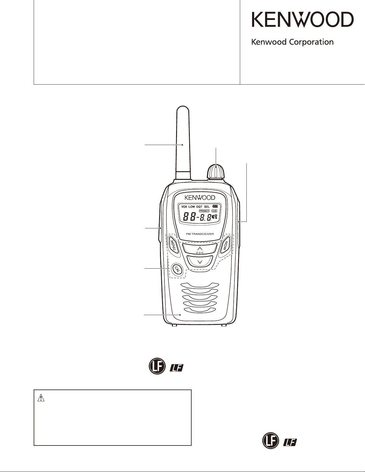
1. Getting Acquainted
PTT (Push to Talk) switch
q
Press and hold, then speak into the speaker area to trans-
mit.
MENU key
w
Press to perform various functions. Press and hold while
switching the power ON to enter Setting Mode.
CAL key
e
Press before making a call to alert the other party mem-
bers, or press to select a unit ID to make a call.
/ keys
r
Press to change the operating channel, to select a menu
in Setting Mode, and to perform other functions.
Power switch/Volume control
t
Turn clockwise to switch the power ON and counter-
clockwise to switch the power OFF. Rotate to adjust the
volume.
MON key
y
Press to monitor the current channel for activity.
LED Indicator
u
Indicates the transceiver status.
SP/MIC jacks
i
Lift the covers and insert the accessory’s plugs here.
模式组合
1. 介绍
PTT(按下通话)开关
q
按住,然后对着扬声器区域讲话来进行发射。
MENU 键
w
按下可执行各种功能。打开电源时按住可进入设置模式。
(经销商须启用设置模式)
CAL 键
e
进行呼叫前按下可提醒其他组员,或按下来选择一个单元
ID 进行呼叫。
/ 键
r
按下可改变工作信道、在设置模式下选择菜单、执行其他
功能。
电源开关 / 音量控制
t
顺时针转动可打开电源,逆时针转动可关闭电源。转动调
节音量。
MON 键
y
按下可监听当前信道的活动状况。
LED 指示灯
u
显示对讲机状态。
SP/MIC 插孔
i
提起盖子,将附件的插头在此插入。
Antenna
天线
:
@
.
Microphone
麦克风
;
2. PC Mode
2-1. Preface
The transceiver is programmed by using a personal computer, a programming interface (KPG-22/22A, USB adapter
(KCT-53U)) and programming software (KPG-108D).
The programming software can be used with an IBM PC
or compatible. Figure 1 shows the setup of an IBM PC for
programming.
2-2. Connection Procedure
1. Connect the transceiver to the personal computer with
the interface cable and USB adapter (when the interface
cable is KPG-22A, the KCT-53U can be used.).
>
=
2
B
Speaker
扬声器
2. PC 模式
2-1. 前言
对讲机采用个人电脑、编程接口 (KPG-22/22A,USB 适配器
(KCT-53U)) 和编程软件 (KPG-108D) 进行编程。
编程软件可以在 IB M P C 或兼容的 PC 上进行使用。图 1 给
出了 IBM PC 进行编程的设置。
2-2. 连接操作
1. 使用接口电缆和 U SB 适配器将对讲机连接到个人电脑 ( 接
口电缆为 KPG-22A 时,可以使用 KCT-53U)。
4

TK-3230
REALIGNMENT /
Notes:
• You must install the KCT-53U driver in the computer to
used the USB adapter (KCT-53U).
• When using the USB adapter (KCT-53U) for the fi rst time,
plug the KCT-53U into a USB port on the computer with
the computer power ON.
2. When the POWER is switched on, user mode can be entered immediately. When the PC sends a command, the
transceiver enters PC mode.
When data is receiving from the transceiver, the red LED
lights.
When data is transmitted by the transceiver, the green
LED lights.
Notes :
• The data stored in the personal computer must match
Model Name when it is written into EEPROM.
• Do not press the [PTT] key during data transmission or
reception.
2-3. KPG-22/KPG-22A Description
(PC programming interface cable : Option)
The KPG-22/22A is required to interface the transceiver
with the computer. It has a circuit in its D-sub connector
(KPG-22: 25-pin, KPG-22A: 9-pin) case that converts the RS232C logic level to the TTL level.
The KPG-22/22A connects the SP/MIC connector of the
transceiver to the RS-232C serial port of the computer.
模式组合
注意 :
• 必须在电脑上安装 K C T -53U 驱动程序才能使用 U S B 适配器
(KCT-53U)。
• 首次使用 U S B 适配器 (KCT-53U ) 时,请在电脑开机的情况
下将 KCT-53U 插入电脑的 USB 端口。
2. 对讲机电源打开时,可以立即进入用户模式。 P C 发送指令
时,对讲机进入 PC 模式。
对讲机发送数据时,红色的 LED 点亮。
对讲机接收数据时,绿色的 LED 点亮。
注意 :
• 个人电脑保存的数据写入 EEPROM 时,必须与机型相符。
• 请勿在数据发送或接收期间按 [PTT] 键。
2-3. KPG-22/KPG-22A 说明
(PC 编程接口电缆 :选购件 )
将对讲机与电脑相连需要 KP G-22/22A。该电缆的 D-sub 连
接器 (KPG-22 :25 针,KPG-22A :9 针 ) 盒具有将 RS -232C 逻
辑电平转换为 TTL 电平的电路。
KP G-22/22A 将对讲机的 SP/MIC 连接器连接到电脑的 R S -
232C 串行端口。
2-4. KCT-53U Description (USB adapter : Option)
The KCT-53U is a cable which connects the KPG-22A to a
USB port on a computer.
When using the KCT-53U, install the supplied CD-ROM
(with driver software) in the computer. The KCT-53U driver
runs under Windows 2000 or XP.
2-5. Programming Software Description
The KPG-108D is the programming software for the transceiver supplied on a CD-ROM. The software on this disk
allows a user to program the transceiver radios via Programming interface cable (KPG-22).
2-6. Programming with IBM PC
If data is transferred to the transceiver from an IBM PC
with the KPG-108D, the data for each set can be modifi ed.
Data can be programmed into the EEPROM in RS-232C
format via the SP/MIC jack.
In this mode the PTT line operate as TXD and RXD data
lines respectively.
2-4. KCT-53U 说明 (USB 适配器 :选购件 )
KCT-53U 是将 KPG-22A 连接到电脑 USB 端口的电缆。
使用 KCT -53U 时,请在电脑上安装附带的 CD-ROM( 带有驱
动程序软件 )。 KCT-53U 驱动程序运行于 Windows 2000 或 XP
下。
2-5. 编程软件说明
KP G-108D 是 CD-ROM 附带的用于对讲机的编程软件。该光
盘上的软件允许用户通过编程接口电缆 (KPG-22) 对对讲机进
行编程。
2-6. 使用 IBM PC 编程
如果使用 KP G -108D 将数据从 I B M P C 传输到对讲机,则每
套对讲机的数据均可修改。
通过 SP/MIC 插孔可以将数据以 RS-232C 格式写入 EEPROM。
在该模式下,PTT 线路分别用作 TXD 和 RXD 数据线路。
5
TK-3230
KPG-108D
REALIGNMENT /
KPG-22 or KPG-22A or KPG-22A+KCT-53U
IBM-PC
Tuning cable / 调谐电缆
(E30-3216-05)
Illustration is KPG-22
插图为KPG-22
Gray
Gray/Black
1.5D-XV Lead wire
1.5D-XV Shield wire
灰色
灰色/黑色
1.5D-XV导线
1.5D-XV屏蔽线
PC
D-SUB
(25-pin)
Transceiver
对讲机
模式组合
+
SP
–
+
MIC
–
KPG-22
Transceiver
PC
D-SUB
(9-pin)
对讲机
PC
USB
KCT-53U
KPG-22A
KPG-22A
Transceiver
对讲机
Fig. 1 /
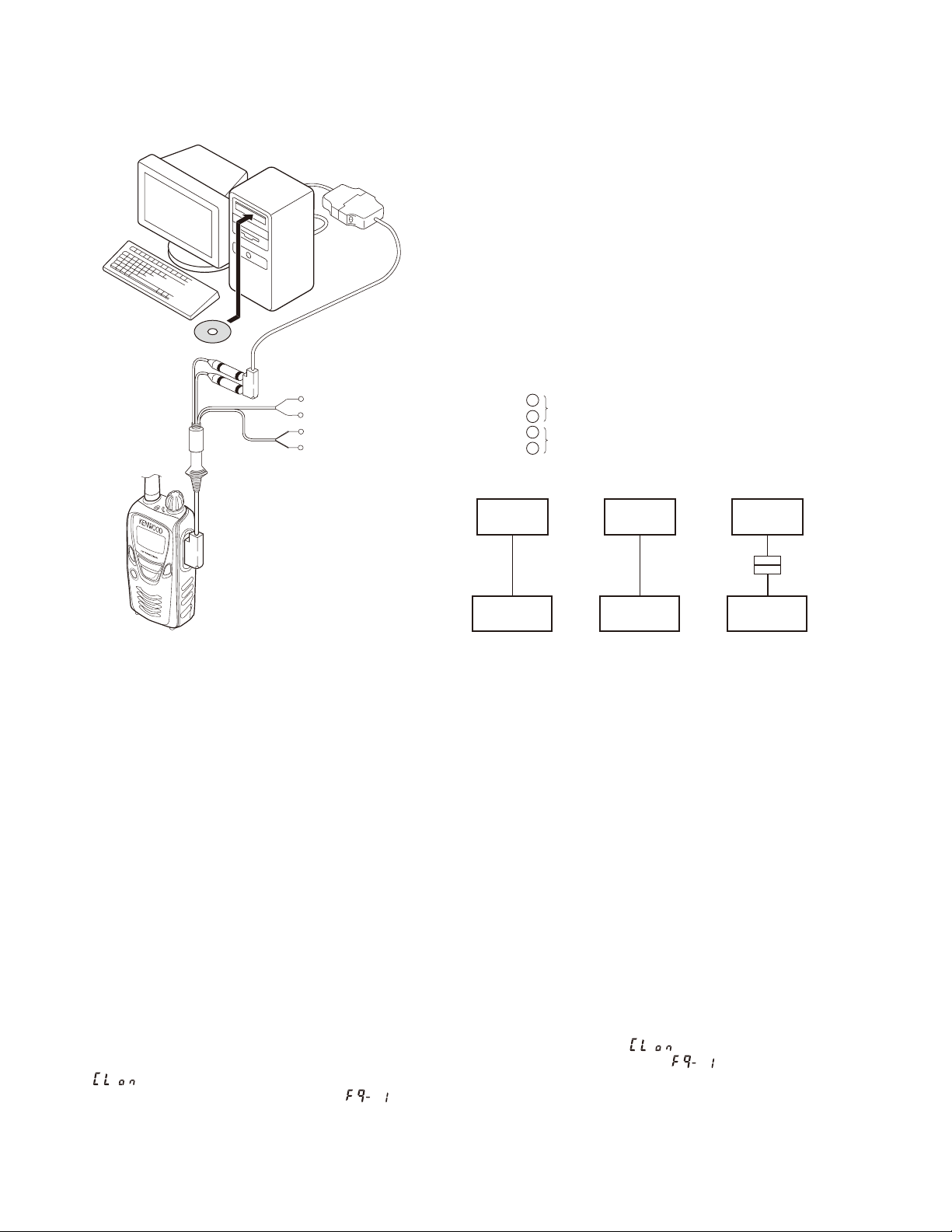
3. Clone Mode
3-1. Outline
”Clone Mode” copies the transceiver data to another
transceiver.
The dealer can copy the transceiver data to another trans-
ceiver even without the use of a personal computer.
3-2. Example
The transceiver can copy the programming data to one or
more transceivers via RF communication.
The clone source and clone target/s must be in Clone
mode.
3-3. Operation
1. To switch the clone target/s to Clone mode, press and
hold the [PTT] and [MONI] keys while turning the transceiver power ON.
2. Keep holding [PTT] and [MONI] keys for 1 second. Transceiver sound key on tone and enters Clone mode with
”
3. Wait for 2 seconds. Transceiver displays ”
4. Select a channel table number using [UP] (increment
channel table) and [DOWN] (decrement channnel table)
keys.
” display.
”.
图1
3. 复制模式
3-1. 概述
“复制模式”能将对讲机数据复制到其他对讲机。
即使没有使用个人电脑,经销商也能将对讲机数据复制到
其他对讲机。
3-2. 实例
通过 R F 通信,对讲机可以将编程数据复制到一台或多台对
讲机。
复制源和复制目标必须均处于复制模式。
3-3. 操作
1. 如需将复制目标切换到复制模式,请在打开对讲机电源的
同时按住 [PTT] 和 [MONI] 键。
2. 按住 [PTT] 和 [MONI] 键 1 秒钟。对讲机响起键音并进入复
制模式,同时显示“
3. 等候 2 秒钟。对讲机显示“
4. 使用 [UP]( 增大信道表 ) 和 [DOWN]( 减小信道表 ) 键选择
信道表号。
”。
”。
6

TK-3230
REALIGNMENT /
5. To switch the clone source to Clone mode, press and
hold the [PTT] and [MONI] keys while turning the transceiver power ON.
6. Keep holding [PTT] and [MONI] keys for 1 second. Transceiver sound key on tone and enters Clone mode with
”
7. Wait for 2 seconds. Transceiver displays ”
8. Select the same channel table number as the clone target/s.
9. Press [PTT] on the clone source to begin data transmission. When the clone target starts to receive data, the
LED will light green.
When the clone source finishes sending data, a
”confi rmation” tone will sound with ”
If data transmission fails while cloning, an ”error” tone
will sound from the Target unit with ”
10
. If the cloning fails, no data will be available in the Target
unit when it is returned to User mode.
11
. When the cloning is successful, the Target unit’s ”Scan”,
”Key Lock” and ”Super Lock” functions will return to
their default values (Scan = OFF, Key Lock = OFF, Super
Lock = OFF).
12
. After clone has completed, it is necessary for the Target
unit to set its required ID Type of ID List for FleetSync.
This can be done by using unit’s ID List Setting Mode.
” display.
”.
” displayed.
” displayed.
模式组合
5. 如需将复制源切换到复制模式,请在打开对讲机电源的同
时按住 [PTT] 和 [MONI] 键。
6. 按住 [PTT] 和 [MONI] 键 1 秒钟。对讲机响起键音并进入复
制模式,同时显示“
7. 等候 2 秒钟。对讲机显示“
8. 选择与复制目标相同的信道表号。
9. 按复制源上的 [PTT] 开始数据发射。复制目标开始接收数
据时,LED 将会点亮绿色。
复制源发送数据完成时,将会响起“确认”音并显示
“
如果复制期间数据发射失败,则复制目标将会响起“错误”
音并显示“
10. 如果复制失败,则复制目标返回到用户模式时没有任何数
据。
11. 复制成功时,复制目标的“扫描”、“按键锁定”和“超级
锁定”功能将会返回到各自的默认值 ( 扫描 =OFF,按键锁
定 =OFF,超级锁定 =OFF)。
12. 复制完成后,复制目标需要设置 FleetSync 对应 ID 列表
的ID类型。
使用对讲机的 ID 列表设置模式即可完成。
”。
”。
”。
”。
Notes:
• The dealer can clone data to two or more transceivers by
repeating the above procedures.
• If the transceiver’s Clone Mode is configured as
”Disabled”, the transceiver cannot enter Clone mode.
• The table shown below will cover the frequencies used
for wireless cloning.
• A unit cannot be a ”Source Unit” if it is unprogrammed. If
[PTT] is pressed, an ”error” tone will sound.
• Once a unit is set to be the Source, it cannot be a target
after the data has been transmitted. This protects the
data in the Source unit.
• If the Target unit is cloned unsuccessfully, ”error” tone
will sound with ”
• After 4 seconds, Target unit returns to display ”
”xx” means the last selected channel table number.
• The Source unit and Target unit must be of the same
model type and destination in order for Clone to operate.
• It is not possible to read/write setup data from the clone
source/target when it is in Clone mode. But it will trigger
to go to cloning mode (TX) when try to read/write.
• Electronic interface may cause a failure in data transfer
during Wireless Clone, such as when waveforms or electromagnetics are being performed at the workbench.
• Clone mode can be used ONLY by the authorized service
personnel.
• The Clone mode setting must be confi gured as ”Disable”
before being delivered to the end-user.
• When wireless Clone mode is used, the environment
must ensure that the radio wave does not leak to outside.
• The transmit output power is automatically set to Low in
Clone mode.
• Battery saver function is automatically set to off in Clone
mode.
” display.
”.
注意 :
• 通过重复上述操作,经销商可以将数据复制到两台或多台
对讲机。
• 如果对讲机的复制模式被配置为“禁用”,则对讲机无法进
入复制模式。
• 下表涵盖无线复制所用的频率。
• 如果未经编程,则对讲机无法成为“复制源”。此时按 [PTT]
将会响起“错误”音。
• 出于保护复制源数据的目的,对讲机一旦被设置为复制源,
则发射数据后无法成为复制目标。
• 如果复制目标没有成功复制,则将会响起“错误”音并显
示“
• 4 秒钟后,复制目标返回“
选择的信道表号。
• 为了能够进行复制操作,复制源和复制目标的机型和型号
必须相同。
• 处于复制模式时,无法读 / 写复制源 / 目标的设置数据。
但在尝试读 / 写时将会触发进入复制模式 (TX)。
• 无线复制期间,电子干扰可能会导致数据传送失败,例如
工作台上存在干扰电波或电磁场等。
• 复制模式只能由授权服务人员使用。
• 交付最终用户之前,复制模式设置必须配置为“禁用”。
• 使用无线复制模式时,必须确保无线电波不会向外部泄漏
的环境。
• 在复制模式下,发射输出功率自动设置为低。
• 在复制模式下,电池省电功能自动设置为关。
”。
”显示。“x x”表示最新
7
TK-3230
CIRCUIT DESCRIPTION /
Frequency Confi guration
ANT
460~470MHz
ANT
SW
RF
AMP
BPF
RF
AMP
Fig. 1 Frequency confi guration /
Double super heterodyne
Reception method
Transmission method VCO direct oscillation amplifi cation
Modulation Variable reactance phase modulation
1st IF frequency 38.85MHz
2nd IF frequency 450kHz
Table 1 Basic confi guration
RF
AMP
421.15~
431.15MHz
460~470MHz
1st MIX
电路说明
频率构成
CF
450kHz
38.85MHz
MCF
MIX, IF
DET
38.4MHz
Tripler
X3
PLL VCO
图 1 频率构成
接收方式
发射方式 VCO 直接振荡放大
调制 可变电抗相位调制
AF
AMP
TCXO
12.8MHz
MIC
AMP
双超外差
第一中频 38.85MHz
第二中频 450kHz
表 1 基本构成
SP
MIC
Receiver System
Front End
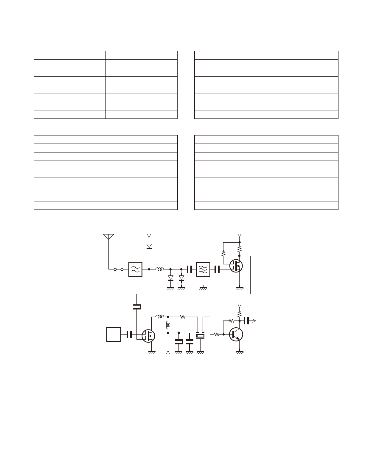
■
The high-frequency signal from the antenna passes
through a low-pass fi lter and a high-frequency switch (D101,
D200, D201 and L220) which switches between transmission and reception, and goes to the BPF (L218) to remove
unwanted signals. The resulting signal is amplifi ed by highfrequency amplifi er (Q204) and goes to the fi rst mixer (Q203).
First Mixer
■
The signal that reaches Q203 is mixed with the fi rst local
signal from the VCO to produce a fi rst IF signal (38.85MHz).
(Receive frequency – First local frequency
= First IF frequency = 38.85MHz)
The fi rst IF signal passes through MCF: XF200 (monolithic
crystal fi lter) to remove unwanted signals.
The fi rst IF signal is amplifi ed by IF amplifi er (Q201) and
goes to IF IC (IC200).
ANT
LPF
ANT
SW
D101
D200
D201
L220
BPF
L218
RF AMP
Q204
1st MIXER
Q203
接收系统
■前端
天线的高频信号通过低通滤波器和高频开关 (D101、D200、
D201 和 L220)( 用于切换发射和接收 ),然后进入 B P F (L218)
消除不需要的信号。最终的信号由高频放大器 (Q204) 进行放
大,然后进入第一混频器 (Q203)。
■第一混频器
到达 Q203 的信号与来自 VCO 的第一本振信号混频,进而产
生第一中频信号 (38.85MHz)。
( 接收信号 – 第一本振信号 = 第一中频 = 38.85MHz)
第一中频信号通过 MCF:XF200( 单片晶体滤波器 ) 消除不需
要的信号。
第一中频信号由中频放大器 ( Q201) 进行放大,然后进入中
频 IC (IC200)。
MCF
XF200
38.85MHz465.0MHz
IF AMP
Q201
IF AMP, DET
IC200
AF AMP
IC303 SP
1st local OSC (PLL) 2nd local OSC
8
Fig. 2 Receiver section confi guration /
图 2 接收部分构成
TK-3230
CIRCUIT DESCRIPTION /
Item Rating
Nominal center frequency (fo) 38.85MHz
Pass bandwidth ±5.0kHz or more at 3dB
Attenuation bandwidth ±18.5kHz or less at 35dB
Ripple 1.0dB or less
Insertion loss 4.0dB or less
Guaranteed attenuation 70dB or more at fo–900kHz
Terminating impedance 610Ω±10% / 3.0pF±0.5pF
Table 2 MCF (L71-0586-05) : TX-RX unit (B/2) XF200
Item Rating
Nominal center frequency (fo) 450kHz
6dB bandwidth ±6.0kHz or more
50dB bandwidth ±12.5kHz or less
Ripple (at 450kHz±4kHz) 2dB or less
Guaranteed attenuation
(at 450kHz±100kHz)
Insertion loss 6dB or less
I/O matching impedance 2.0k
Table 3 Ceramic fi lter (L72-0958-05) : TX-RX unit (B/2) CF200
35dB or more
Ω
电路说明
项 目 额 定
标称中心频率 (fo) 38.85MHz
通过带宽 3dB 时 ±5.0kHz 或更大
衰减带宽 35dB 时 ±18.5kHz 或更小
纹波 1.0dB 或更小
插入损耗 4.0dB 或更小
保证衰减 fo-900kHz 时 70dB 或更大
终端阻抗 610Ω±10% / 3.0pF±0.5pF
表 2 MCF(L71-0586-05): TX-RX 单元 (B/2)XF200
项 目 额 定
标称中心频率 (fo) 450kHz
6dB 带宽 ±6.0kHz 或更大
50dB 带宽 ±12.5kHz 或更小
纹波 (450kHz±4kHz 时 ) 2dB 或更小
保证衰减
(450kHz±100kHz 时 )
插入损耗 6dB 或更小
I/O 匹配阻抗 2.0kΩ
表 3 陶瓷滤波器 (L72-0958-05): TX-RX 单元 (B/2)CF200
35dB 或更大
ANT
VCO
1st local
OSC
3T 3R
D101
LPF
L220
D201
1st IF : 38.85MHz
Q203
3R
Fig. 3 Receiver circuit / 图3
IF Amplifi er
■
The IF circuit is integrated in the FM IC (IC200). The IF
IC contains local input, mixer, limiter amplifi er, FM DET, and
low-frequency amplifi er.
The IF signal coming from the IF amplifi er (Q201) goes
to the IF IC mixer and is mixed with the second local signal (38.4MHz) to produce a second IF signal. (38.85MHz –
38.4MHz = 450kHz)
The tripled PLL reference oscillation (12.8MHz x 3) is
used for the second local signal.
L218
BPF
Q204
D200
3R
IF IC
XF200
Q201
接收电路
■中频放大器
中频电路集成在 FM IC (IC200) 内部。中频 IC 内含本地输入、
混频器、限幅放大器、FM DET 和低频放大器。
来自中频放大器 (Q201) 的中频信号随后进入中频 IC 并
与第二本振信号 (38.4MHz) 混频,进而产生第二中频信号。
(38.85MHz - 38.4MHz = 450kHz)
三倍 PLL 基准振荡 (12.8MHz x 3) 用于第二本振信号。
9
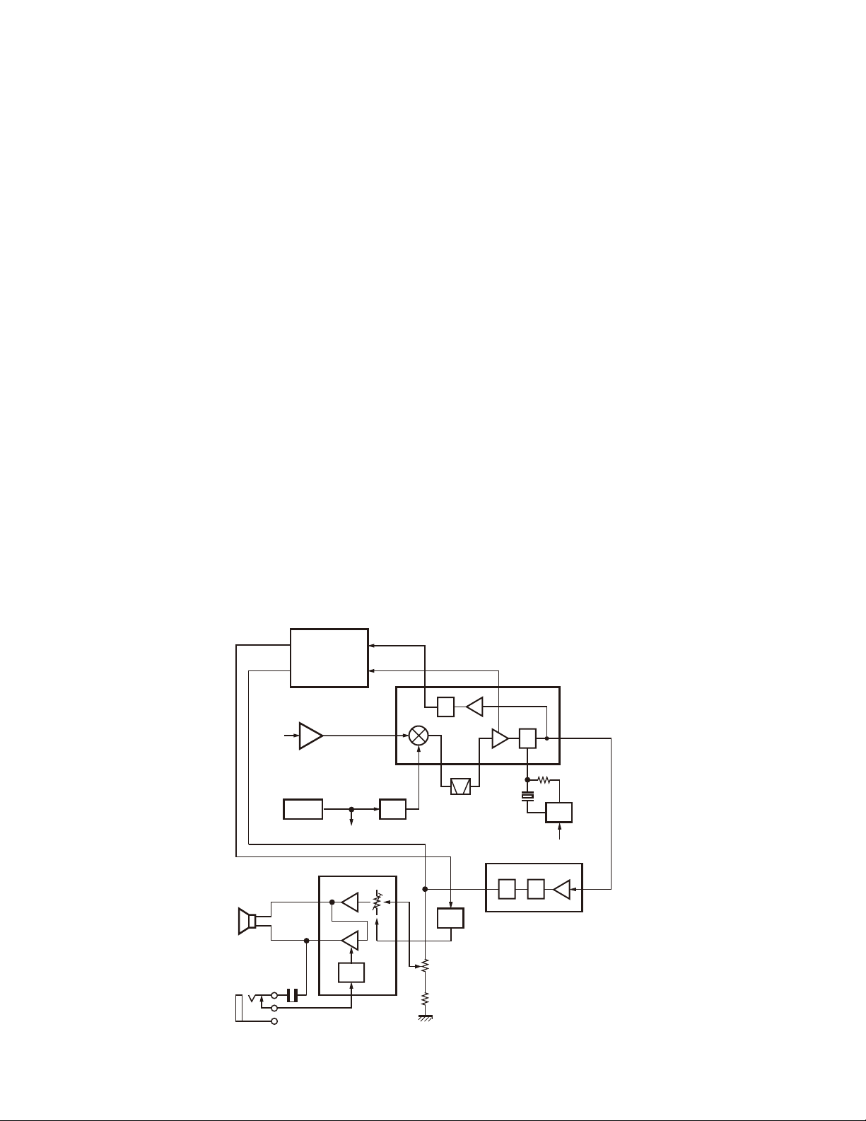
TK-3230
CIRCUIT DESCRIPTION /
The second IF signal passes through ceramic fi lter (CF200)
to remove unwanted signals.
The second IF signal passing through the ceramic fi lter
passes through the limiter amplifi er consisting six differential amplifi ers and is detected.
The amplified second IF signal is demodulated by the
quadrature detector with the ceramic discriminator (CD200).
The demodulated signal is routed to the audio circuit.
Squelch Circuit
■
A squelch circuit is provided to prevent no-signal noise or
weak signals from outputting to a speaker during transmission.
AF Circuit
■
The FM IC output passes through the base band IC
(IC300). The signal then goes through an AF volume control, and is routed to an audio power amplifi er (IC303) where
it is amplfi ed and output to speaker. This IC have BTL amplifi er function. At internal speaker, BTL amplifi ed. At external
speaker, IC switch off the 1 channel amplifi er by connectors
information.
Narrow and wide setting can be made for each channel
by switching the demodulation level. The WIDE (low level)
and NARROW (high level) data is output from IC403, pin
69. When a Wide (low level) data is received, Q200 turn on.
When a NARROW (high level) data is received, Q200 turn
off.
Q200 turns off/on with the wide/narrow data and the
IC200 detector output level is switched to maintained a constant output level during wide or narrow signals.
电路说明
第二中频信号通过陶瓷滤波器 (CF200) 消除不需要的信号。
通过陶瓷滤波器的第二中频信号随后通过由六个不同放大
器组成的限幅放大器并进行检测。
放大后的第二中频信号由积分检波器通过陶瓷鉴频器
(CD200) 进行解调。已解调的信号转发给音频电路。
■静噪电路
静噪电路用于防止无信号的噪声或微弱信号输出到扬声器。
■AF电路
FM I C 输出信号通过基带 I C (IC300)。随后信号通过 AF 音
量调整,并发送给音频功率放大器 (IC303),在这里经过放大
并输出到扬声器。该 IC 具有 BTL 放大器功能。在内部扬声器,
BT L 被放大。在外部扬声器,IC 通过连接器信息关闭 1 信道
放大器。
通过切换解调电平,各个信道均可进行窄宽设置。宽信号
( 低电平 ) 及窄信号 ( 高电平 ) 数据从 IC403( 针脚 69) 输出。
接收到宽信号 ( 低电平 ) 数据时,Q200 打开。接收到窄信号 ( 高
电平 ) 数据时,Q200 关闭。
在宽或窄信号期间,Q200 随宽 / 窄信号数据打开 / 关闭,
IC200 检波器输出电平切换为保持恒定输出电平。
SP AMP
BEEP
1st IF
INT. SP
J300
EXT. SP
52
IC403
MCU
Q201
IF amp
X1
38.85
MHz
12.8MHz
PLL
IC303
Amp
Amp
SW
76
7512
MIXIN
38.4MHz
BUSY
RSSI
16
Q202
X3TCXO
MIX
CF200
450kHz
RXAF
VR301
AF VR
Q301
Amp
10
CD200
IC300
HPF LPF
DET
IC200
W/N
9
AFOUT
Q200
SW
Amp
AF
23
RXIN
10
Fig. 4 IF amplifi er, Squelch and AF circuits / 图4
中频放大器 , 静噪 , AF 电路
TK-3230
CIRCUIT DESCRIPTION /
Transmitter System
Microphone Amplifi er Circuit
■
The audio signal from the microphone passes through
the MIC amplifi er (IC302). Then, the signal goes through the
base band IC (IC300) that has the 6dB/oct pre-emphasis circuit, band-pass fi lter (300 to 3kHz), amplifi er, and limiter. The
distortion components outside the audio band are removed
by the splatter fi lter.
Modulation Circuit
■
The MIC amplifi er (IC302) output passes through VR300
for modulation adjustment and goes to the modulation input
of the VCO circuit for variable reactance phase modulation.
Transmission Output Circuit
■
The VCO output is amplifi ed by a high-frequency amplifi er
(Q101, Q103 and Q104), passes through a high-frequency
antenna switch, passes through a low-pass fi lter and goes
to the antenna.
The transmission output is about 1.5W with 3.8V DC supply at battery terminal.
Low-Pass Filter Circuit
■
A three-stage Chebyshev type low-pass fi lter is located
between the antenna and transmit/receive switching circuit.
It removes harmonic components contained in the transmission output.
MIC AMP
IC302MIC
电路说明
发射系统
■麦克风放大器电路
麦克风的音频信号通过麦克风放大器 ( IC302)。随后信号
通过具有 6dB/oct 预加重电路、带通滤波器 (300 ~ 3kHz)、
放大器和限幅器的基带 IC ( I C300)。音频频带外的失真成分
由边带滤波器进行消除。
■调制电路
麦克风放大器 (IC302) 输出信号通过 VR300 进行调制调整,
然后进入 VCO 电路的调制输入进行可变电抗相位调制。
■发射输出电路
VCO 输出信号由高频放大器 (Q101、Q103 和 Q104) 进行放大,
然后依次通过高频天线开关和低通滤波器并进入天线。
电池端子采用 3.8V 直流供电时,发射输出功率约为 1.5W。
■低通滤波电路
三阶切比雪夫低通滤波器位于天线和发射 / 接收切换电路
之间,能够消除发射输出信号中所带的谐波成分。
VCO
Q2,Q5VR300
RF AMP
Q6
PRE-DRIVE
AMP
Q101
DRIVE
AMP
Q103
FINAL
AMP
Q104
ANT SW
D101,D200,
D201
LPF
Fig. 5 Transmitter section confi guration / 图5
IC300
Amp
麦克风放大器电路
SW
IC302
D301
DET
MIC
Q303
MIC
MUTE
D303
MIC amp
Fig. 6 Microphone amplifi er circuit / 图6
ANT
发射部分构成
LPFIDC
11
TK-3230
CIRCUIT DESCRIPTION /
PLL System
VCO Circuit
■
The VCO is housed in a shield case.
The VCO circuit consists of a transistor (Q2), a variable
capacity diode (D2) for frequency control, a variable capacity
diode (D4) for modulation, transmit/receive frequency shift
diode (D1), control transistor (Q1) and oscillator buffer amplifi er (Q5).
In receive mode, the shift signal T/R goes low, Q1 turns
off, and the shift diode (D1) not contact. Q2 produces the
fi rst local frequency for reception. (Receive channel frequency – 38.85MHz)
In transmit mode, the shift signal T/R goes high, Q1
turns on and D1 does conducts. Q2 produces about
460~470MHz and the VCO frequency equals the transmit
channel frequency.
The 3.0V circuit voltage is produced by ripple removing
fi lter circuit Q4.
C14
LV
T/R
R1
R6
L15
C57
C453
L2
C4
L4
D2
L3
C59
R11
电路说明
PLL 系统
■ VCO 电路
VCO 外嵌屏蔽罩。
VC O 电路由晶体管 ( Q2)、用于频率控制的可变电容二极管
(D2)、用于调制的可变电容二极管 ( D4)、发射 / 接收频率偏
移二极管 (D1)、控制晶体管 (Q1) 和振荡缓冲放大器 (Q5) 组成。
在接收模式下,移位信号 T/R 变低,Q1 关闭并且二极管 (D1)
不导通。Q2 产生用于接收的第一本振频率。( 接收信道频率
- 38.85MHz)
在发射模式下,移位信号 T / R 变高,Q1 打开并且 D1 导通。
Q2 产生 460 ~ 470MHz 的频率并且 VCO 频率与发射信道频率相
同。
由纹波消除滤波电路 Q4 产生 3.0V 的电路电压。
C18
D4
R17
L5
R20
R21
R22
C22
L6
C27
Q2
L8
C28
R27
C33
R29
Q5
C31
VCO
OUT
L10
R31L16
R2
C5
D1
Q1
C15
R23
R7
MOD
3C
Fig. 7 VCO circuit / 图7
PLL Circuit
■
Frequency data is sent to the PLL IC (IC1) from the MCU
(IC403) as serial data when the power turns on, when the
channel is changed, or when transmission begins. It sets
the variable divider in the PLL IC.
The TCXO (X1) produce a 12.8MHz reference frequency.
It is divided to produce a 6.25kHz/5kHz PLL comparison frequency in the PLL IC.
This PLL IC can generate a channel step which is twice of
the PLL comparison frequency. Hence, the PLL IC can directly generate channel step by 12.5kHz/10kHz. Beside, an
external control voltage of TCXO is used to shift TCXO reference frequency by 6.25kHz/5kHz to achive channel step
with 6.25kHz/5kHz generate in the PLL IC.
R12
C19
C56
R25
C24
D5
C29
C36
Q4
C39C40
+
C451
VCO 电路
■ PLL 电路
电源打开时,信道改变时,或发射开始时,MCU (IC403) 的
频率数据作为串行数据发送到 PLL IC (IC1),设置 PLL IC 中
的可变分频器。
TCXO (X1) 产生 12.8M H z 基准频率,随后在 P L L I C 中分频
产生 6.25kHz/5kHz 的 PLL 比较频率。
该 P LL IC 可以产生两倍于 PLL 比较频率的信道步长。因
此,PLL IC 可以直接产生 12.5kHz/10kHz 的信道步长。此外,
TCXO 的外部控制电压用于偏移 6.25kHz/5kHz 的 TCXO 基准频
率,进而实现在 PLL IC 中产生 6.25kHz/5kHz 的信道步长。
12
TK-3230
CIRCUIT DESCRIPTION /
The VCO output is divided by the divide ratio set by the
divider in the PLL IC to generate 6.25kHz/5kHz. It is compared with the reference comparison frequency by the
phase comparator to detect a phase difference.
The charge pump circuit in the PLL IC converts it to a
control voltage that can drive the VCO directly.
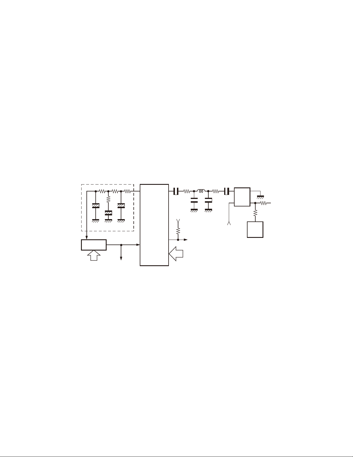
The control voltage passes through a loop filter which
passes low frequency and is applied to the VCO control pin
to control the oscillator frequency. The loop fi lter removes
unwanted harmonics and noise contained in the output from
the phase comparator and determines PLL response and
synchronizing characteristics by the amplitude and phase
characteristics (Fig. 8).
Unlock Detection Circuit
■
If the PLL cannot be synchronized for some reason or
other when switching the channel or changing between
transmission and reception, the PLL IC outputs a low unlock detection signal. This signal goes to the MCU to inhibit
transmission when the PLL is unlocked.
CP1 XIN
++
+
FIN1
PLL IC
IC1
LD
STB
DATA
CK
Loop filter
LV
VCO
3C,T/R,MOD
F OUT
VCO OUT
电路说明
VCO 输出信号由 PLL IC 中分频器设置的分频倍率进行分频,
进而产生 6.25kHz/5kH z 的频率,随后由相位比较器与基准比
较频率进行比较来检测相位差。
PLL IC 中的电荷泵电路将其转换为可以直接驱动 VC O 的控
制电压。
控制电压通过环路滤波器,经过低频并应用到 V CO 控制针
脚来控制振荡频率。环路滤波器消除相位比较器输出信号中
所带的不需要的谐波和噪音,并由振幅及相位特性确定 P L L
响应及同步特性(图8)。
■失锁检测电路
切换信道或在发射与接收之间进行切换时,如果由于某些
其他原因造成 PLL 无法同步,则 PLL I C 会输出低失锁检测信
号。PLL 失锁时,该信号进入 MCU 禁止发射。
X1 12.8MHz
TCXO
TO
3C
3M
MCU (IC403)
UL
PLL data
(MCU)
IC100
DAC
Fig. 8 PLL circuit / 图8
Control System
Reset Circuit
■
When a battery voltage is dropped, IC401 is detected low
voltage, and this detected signal input to IC403 for stop the
MCU function. IC400 is detected the reset voltage.
Battery Voltage Detection Circuit
■
The unit detects a low battery voltage and display the
BATT indicator on the LCD. The battery voltage is divided
and applied to the analog value input pin (BATT) of the MCU,
and converted to a digital signal.
Power Supply Circuit
■
The power supply voltage is maintained to 3.0V by the
series regulator (IC404). It is used as MCU power 3M, 3C,
3R and 3T.
The B (battery voltage) is supplied to the RF fi nal transistor Q104.
PLL 电路
控制系统
■复位电路
电池电压下降时,I C401 检测到低电压并且该检测信号输
入到 IC403 用于停止 MCU 功能。IC400 检测复位电压。
■电池电压检测电路
本单元检测低电压并在 LCD 上显示 BATT 指示。电池电压随
后进行划分并应用到 MCU 的模拟数值输入针脚 (BATT),然后
转换为数字信号。
■电源电路
电源电压由串联稳压器 (I C404) 稳压至 3.0V,用作 M CU 电
源 3M、3C、3R 和 3T。
B(电池电压)为RF末级晶体管 Q104 供电。
13

TK-3230
CIRCUIT DESCRIPTION /
The transmission power 3T is supplied to the transmission output circuit when the MCU turns Q404 on only in
transmit mode.
The reception power 3R is provided to the receive and IF
circuits when the MCU turns Q406 on only in receive mode.
The transmission/reception power 3C is supplied to the
VCO and PLL circuits when the MCU turns Q405 on in
transmit and receive modes.
If no signal is received for 10 seconds, the MCU enters
the power save mode, and turns common power 3C and
reception power 3R on for one cycle and off for three cycles
according to the signals from the MCU to save the battery
power.
QT/DQT
■
• Encode (Transmit)
QT/DQT signal is generated by MCU (IC403). Output signal (IC403 pin 18 (TO)) goes to TCXO modulation and VCO
modulation (Through the VR300).
• Decode (Receive)
Detected AF signal go to IC300 and then IC301. Function
of IC301 is LPF for sub-audible frequency. This signal goes
to IC403 pin 77 (TI). IC403 is detected the QT or DQT.
电路说明
仅在发射模式下 M C U 打开 Q404 时,发射电源 3T 才为发射
输出电路供电。
仅在接收模式下 M C U 打开 Q406 时,接收电源 3R 才为接收
及中频电路供电。
在发射和接收模式下 MCU 打开 Q405 时,发射 / 接收电源
3C 为 VCO 及 PLL 电路供电。
如果 10 秒钟内没有接收到任何信号,M C U 进入省电模式,
然后根据 M CU 的信号循环打开公共电源 3C 和接收电源 3R 一
段时间长度而后关闭三段时间长度,从而达到节省电池电量
的目的。
■ QT/DQT
●编码(发射)
QT/DQT 信号由 MCU (IC403) 产生。输出信号 ( IC403 针脚
18) 进入 TCXO 调制和 VCO 调制 ( 通过 VR300)。
●解码(接收)
检测到的 AF 信号进入 IC300 并随后进入 I C301。I C301 的
功能为用于亚音频的 LP F。该信号进入 I C403 针脚 77 (TI)。
IC403 检测 QT 或 DQT。
B
IC403
MCU
Power
SW
BATT
IC404 Q405
AVR SW
Q406
SW
Q404
SW
SB
3M
3C
3R
3T
Fig. 9 Reset, Battery voltage detection and
Power supply circuits
图9 复位 , 电池电压检测 , 电源电路
VR300
IC300
Baseband
IC
IC403
MCU
TO
18
LPF
IC301 IC200
77
TI
LPF
Fig. 10 QT/DQT circuit / 图10
TCXO
VCO
TX AF
IF IC
QT/DQT 电路
14
TK-3230
SEMICONDUCTOR DATA /
MCU: D338327A22WV (TX-RX unit IC403)
Terminal Function
■
Pin No. Signal Name I/O Function
1 SP DET I Head set detect
2 AVSS - GND
3X1 -
4X2 -
5 VSS - GND
6 OSC2 - X’tal (7.3728MHz)
7 OSC1 - X’tal (7.3728MHz)
8 TEST I
9 RESET - Reset
10 SCLK O Serial clock
11 POW CON O Auto power control
12 BEEP O Beep output
13 DIR O DIR to IC300
14 SDATA I/O Serial data
15 TDATA O MSK TX data
16 TCLK I TCLK from IC300
17 RDF I RDF/FD
18 TO O QT/DQT output
19 PWM IN I PWM data input
20 BOOT I BOOT/USER input
21 SAVE O Battery save
22 3RC O 3R control
23 3TC O 3T control
24 GLED O Green LED
25 RLED O Red LED
26 CVCC - +3V (Power supply)
27 VSS - GND
28~31 V3~V0 -
32 VCC O +3V (Power supply)
33 BACK LT O Back light
34~36 COM3~COM1 -
37 PTT I
38 UP I
39 DOWN I
40 MONI I
41 MENU I
42 CALL I
43 EEPDATA I/O EEPROM data
44 EEPCLK O EEPROM clock
半导体数据
MCU: D338327A22WV(TX-RX 单元 IC403)
■端子功能
管脚号 信号名称
1 SP DET 输入 耳机检测
2 AVSS - GND
3X1 -
4X2 -
5 VSS - GND
6 OSC2 - 晶体 (7.3728MHz)
7 OSC1 - 晶体 (7.3728MHz)
8 TEST 输入
9 RESET - 复位
10 SCLK 输出 串行时钟
11 POW CON 输出 自动功率控制
12 BEEP 输出 提示音输出
13 DIR 输出 DIR 到 IC300
14 SDATA
15 TDATA 输出 MSK TX 数据
16 TCLK 输入 来自 IC300 的 TCLK
17 RDF 输入 RDF/FD
18 TO 输出 QT/DQT 输出
19 PWM IN 输入 PWM 数据输入
20 BOOT 输入 BOOT/USER 输入
21 SAVE 输出 电池节电
22 3RC 输出 3R 控制
23 3TC 输出 3T 控制
24 GLED 输出 绿色 LED
25 RLED 输出 红色 LED
26 CVCC - +3V( 电源 )
27 VSS - GND
28~31 V3~V0 -
32 VCC 输出 +3V( 电源 )
33 BACK LT 输出 背光
34 ~ 36 COM3 ~ COM1 -
37 PTT 输入
38 UP 输入
39 DOWN 输入
40 MONI 输入
41 MENU 输入
42 CALL 输入
43 EEPDATA
44 EEPCLK 输出 EEPROM 时钟
输入/输出
输入/输出
输入/输出
功 能
串行数据
EEPROM 数据
15
TK-3230
SEMICONDUCTOR DATA /
Pin No. Signal Name I/O Function
45 MIC MUTE O MIC mute
46 SHIFT O Beat shift
47 PDATA O Serial data
48 PCLK O Serial clock
49 PEN O PLL IC chip select
50 3MSC O IC300 power supply
51 PABC O Final switch
52 SP AMP O AF AMP on/off
53~68 SEG - LCD
69 WIDE O Wide/Narrow
70 RXD I RXD
71 TXD O TXD
72 BATT L I Battery low
73 AVCC - +3V (AD power supply)
74 THP I TX thermal input
75 RSSI I RSSI input
76 BUSY I Squelch input
77 TI I QT/DQT input
78 BATT I Battery voltage
79 VOX I VOX level
80 UL I PLL unlock detect
半导体数据
管脚号 信号名称
45 MIC MUTE 输出 麦克风静音
46 SHIFT 输出 拍频偏移
47 PDATA 输出 串行数据
48 PCLK 输出 串行时钟
49 PEN 输出 PLL IC 芯片选择
50 3MSC 输出 IC300 电源
51 PABC 输出 末级开关
52 SP AMP 输出 AF AMP 打开 / 关闭
53 ~ 68 SEG - LCD
69 WIDE 输出 宽 / 窄
70 RXD 输入 RXD
71 TXD 输出 TXD
72 BATT L 输入 电池低电量
73 AVCC - +3V(AD 电源 )
74 THP 输入 TX 热感输入
75 RSSI 输入 RSSI 输入
76 BUSY 输入 静噪输入
77 TI 输入 QT/DQT 输入
78 BATT 输入 电池电压
79 VOX 输入 VOX 电平
80 UL 输入 PLL 失锁检测
输入/输出
功 能
FET: RQA0004PXDQS (TX-RX unit Q103)
Absolute Maximum Rating (Ta=25°C)
■
Item V
Rating 16V ±5V 0.3A
DSS
V
GSSID
P
D
3W
Tc=25°C
Tch Tstg
150°C –55~+150°C
FET: RQA0002DNS (TX-RX unit Q104)
Absolute Maximum Rating (Ta=25°C)
■
Item V
Rating 16V ±5V 3.8A
DSS
V
GSSID
Pch Tch Tstg
15W
Tc=25°C
150°C –55~+150°C
FET: RQA0004PXDQS(TX-RX 单元 Q103)
■绝对最大额定值 (Ta=25℃ )
项目 V
额定值 16V ±5V 0.3A
DSS
V
GSS
I
D
P
D
3W
Tc=25℃
Tch Tstg
150℃
–55 ~
+150℃
FET: RQA0002DNS(TX-RX 单元 Q104)
绝对最大额定值 (Ta=25℃ )
■
项目 V
额定值 16V ±5V 3.8A
DSS
V
GSS
I
Pch Tch Tstg
D
15W
Tc=25℃
150℃
–55 ~
+150℃
16
TK-3230
COMPONENTS DESCRIPTION /
TX-RX unit (X57-7330-10)
Ref. No. Part Name Description
IC1 IC Phase Locked Loop system
IC100 IC DAC
IC200 IC IF System
IC300 IC Base Band
IC301 IC Active Filter
IC302 IC MIC amplifi er/ Limiter
IC303 IC Audio Power Amplifi er
IC400 IC Voltage Detect
IC401 IC Reset Switch
IC403 IC MCU
IC404 IC Voltage Regulator (3V)
IC405 IC Divider
IC406 IC EEPROM
Q1 Transistor DC switch (T/R)
Q2 Transistor VCO
Q3 Transistor RF amplifi er
Q4 Transistor Ripple fi lter
Q5 Transistor RF buffer amplifi er
Q6 Transistor RF amplifi er
Q101 Transistor TX pre-drive
Q103 FET TX drive
Q104 FET TX fi nal
Q200 Transistor RX W/N Switch
Q201 Transistor IF amplifi er
Q202 Transistor Tripler
Q203 FET Mixer
Q204 FET RF amplifi er
Q300,301 FET Audio mute switch
Q302 FET VOX switch
Q303 Transistor MIC mute/AGC
Q400 Transistor DC switch (Back Light)
Q401 Transistor DC switch (Busy)
Q402 Transistor DC switch (TX)
Q403,408 Transistor Beat shift switch
Q404 Transistor DC switch (3T)
Q405 Transistor DC switch (3C)
Q406 Transistor DC switch (3R)
D1 Diode Current Steering
D2
Variable capacitance Diode
Frequency control
元件说明
TX-RX 单元 (X57-7330-10)
有关号码 名 称 说 明
IC1 IC 锁相环路系统
IC100 IC DAC
IC200 IC 中频系统
IC300 IC 基带
IC301 IC 有源滤波器
IC302 IC 麦克风放大器 / 限幅器
IC303 IC 音频功率放大器
IC400 IC 电压检测
IC401 IC 复位开关
IC403 IC MCU
IC404 IC 稳压器 (3V)
IC405 IC 分频器
IC406 IC EEPROM
Q1 晶体管 直流开关 (T/R)
Q2 晶体管 VCO
Q3 晶体管 RF 放大器
Q4 晶体管 纹波滤波器
Q5 晶体管 RF 缓冲滤波器
Q6 晶体管 RF 放大器
Q101 晶体管 TX 预驱动
Q103 场效应管 TX 驱动
Q104 场效应管 TX 末级
Q200 晶体管 RX W/N 开关
Q201 晶体管 中频放大器
Q202 晶体管 三倍频器
Q203 场效应管 混频器
Q204 场效应管 RF 放大器
Q300,301 场效应管 音频静音开关
Q302 场效应管 VOX 开关
Q303 晶体管 麦克风静音 /AGC
Q400 晶体管 直流开关 ( 背光 )
Q401 晶体管 直流开关 ( 繁忙 )
Q402 晶体管 直流开关 (TX)
Q403,408 晶体管 拍频偏移开关
Q404 晶体管 直流开关 (3T)
Q405 晶体管 直流开关 (3C)
Q406 晶体管 直流开关 (3R)
D1 二极管 电流导引
D2 可变电容二极管 频率控制
17
 Loading...