

UHF FM TRANSCEIVER
TK-3212L
SERVICE MANUAL
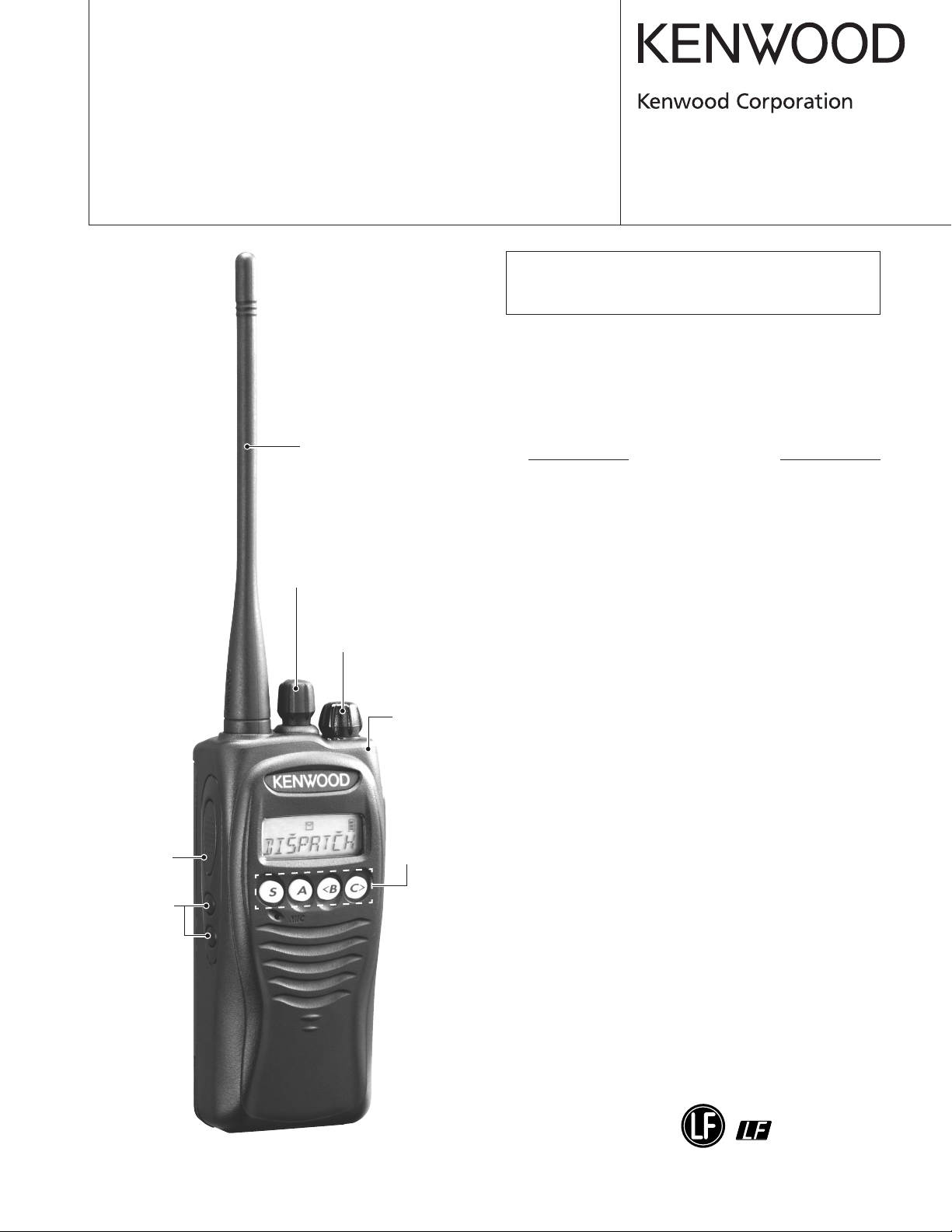
Whip antenna
(T90-1039-15): K,M
(T90-1040-15): K2,M2
Knob (CH)
(K29-9345-04)
Knob (Volume)
(K29-9309-03)
Button knob
(PTT)
(K29-9308-23)
Button knob
(Side1/Side2)
(K29-9364-03)
Plastic cabinet assy
(A02-3894-43)
Key top
(K29-9346-02)
© 2007-3 PRINTED IN JAPAN
B51-8786-00 (S) 508
Refer to the TK-3212/3217 service manual (B51-8716-00)
for any information which has not been covered in this
TK-3212L service manual.
CONTENTS
GENERAL ............................................................. 2
SYSTEM SET-UP ................................................. 2
REALIGNMENT .................................................... 3
CIRCUIT DESCRIPTION ....................................... 8
PARTS LIST .......................................................... 9
EXPLODED VIEW ............................................... 16
PACKING ............................................................ 17
ADJUSTMENT ................................................... 18
PC BOARD
TX-RX UNIT (X57-7130-XX) ......................... 24
SCHEMATIC DIAGRAM ..................................... 28
BLOCK DIAGRAM .............................................. 32
LEVEL DIAGRAM ............................................... 34
OPTIONAL ACCESSORIES
KSC-35 (RAPID CHARGER) .......................... 35
KNB-45L (Li-ion BATTERY PACK) ............... 35
SPECIFICATIONS ............................ BACK COVER
This product uses Lead Free solder.
TK-3212L
GENERAL / SYSTEM SET-UP
DOCUMENT COPYRIGHTS
Copyright 2007 by Kenwood Corporation. All rights
reserved.
No part of this manual may be reproduced, translated,
distributed, or transmitted in any form or by any means,
electronic, mechanical, photocopying, recording, or otherwise, for any purpose without the prior written permission
of Kenwood.
DISCLAIMER
While every precaution has been taken in the preparation
of this manual, Kenwood assumes no responsibility for
errors or omissions. Neither is any liability assumed for damages resulting from the use of the information contained
herein. Kenwood reserves the right to make changes to any
products herein at any time for improvement purposes.
INTRODUCTION
SCOPE OF THIS MANUAL
This manual is intended for use by experienced technicians
familiar with similar types of commercial grade
communications equipment. It contains all required service
information for the equipment and is current as of the
publication date. Changes which may occur after publication
are covered by either Service Bulletins or Manual Revisions.
These are issued as required.
SYSTEM SET-UP
ORDERING REPLACEMENT PARTS
When ordering replacement parts or equipment information,
the full part identification number should be included. This
applies to all parts, components, kits, or chassis. If the part
number is not known, include the chassis or kit number of
which it is a part, and a sufficient description of the required
component for proper identification.
PERSONAL SAFETY
The following precautions are recommended for personal
safety:
●
DO NOT transmit until all RF connectors are verified secure
and any open connectors are properly terminated.
●
SHUT OFF and DO NOT operate this equipment near
electrical blasting caps or in an explosive atmosphere.
●
This equipment should be serviced by a qualified technician only.
SERVICE
This transceiver is designed for easy servicing. Refer to
the schematic diagrams, printed circuit board views, and
alignment procedures contained within.
Unit
Model
& destination
TK-3212L
TK-3212L
TX-RX Unit Frequency range Remarks
K,M X57-7130-12 450~490MHz
K2,
X57-7130-13 470~512MHz
M2
IF1 : 38.85MHz
LOC : 38.4MHz
Merchandise received
License and frequency allocated by FCC
Choose the type of transceiver
Transceiver programming
A personal computer (IBM PC or compatible), programming
interface (KPG-22/22A), USB adapter (KCT-53U), and programming
software (KPG-100D) are required for programming.
(The frequency, TX power HI/LOW, and signaling data are programmed
for the transceiver.)
Are you using the optional antenna?
NO
Are you using the speaker microphone?
NO
Delivery
2
YES
YES
Frequency range (MHz) RF power Type
TX/RX 450~490
TX/RX 470~512
KRA-23 or KRA-27
Optional antenna
(Option)
KMC-17 or KMC-21
Speaker microphone
(Option)
4.0W
4.0W
TK-3212L (K,M)
TK-3212L (K2,M2)
REALIGNMENT
TK-3212L
1. Modes
User mode
PC mode
Clone mode
Self programming mode
Firmware version information
Mode Function
User mode For normal use.
PC mode Used for communication between the
Data programming Used to read and write frequency data
mode
PC test mode Used to check the transceiver using
Clone mode Used to transfer programming data
Self programming You can program the frequency,
mode signaling and other functions using
Firmware version Used to confirm the internal firmware
information version.
Data programming
mode
PC test mode
transceiver and PC (IBM compatible).
and other features to and from the
transceiver.
the PC.
This feature is included in the FPU.
from one transceiver to another.
only the transceiver.
PC tuning mode
Notes:
•
You must install the KCT-53U driver in the computer to use
the USB adapter (KCT-53U).
•
When using the USB adapter (KCT-53U) for the first time,
plug the KCT-53U into a USB port on the computer with the
computer power ON.
2. When the POWER is switched on, user mode can be
entered immediately. When the PC sends a command,
the transceiver enters PC mode.
When data is transmitting from the transceiver, the red
LED lights.
When data is received by the transceiver, the green LED lights.
Notes:
• The data stored in the computer must match the model
type when it is written into the EEPROM.
• Change the transceiver to PC mode, then attach the
interface cable.
3-3. KPG-22/KPG-22A description
(PC programming interface cable: Option)
The KPG-22/22A is required to interface the transceiver with
the computer. It has a circuit in its D-sub connector (KPG-22 :
25-pin, KPG-22A : 9-pin) case that converts the RS-232C logic
level to the TTL level.
The KPG-22/22A connects the SP/MIC connector of the
transceiver to the RS-232C serial port of the computer.
2. How to Enter Each Mode
Mode Operation
User mode Power ON
PC mode Received commands from PC
Clone mode [<B]+Power ON (Two seconds)
Self programming mode
Firmware version [Side1]+[Side2]+Power ON
information (Two seconds)
[S]+Power ON (Two seconds)
3. PC Mode
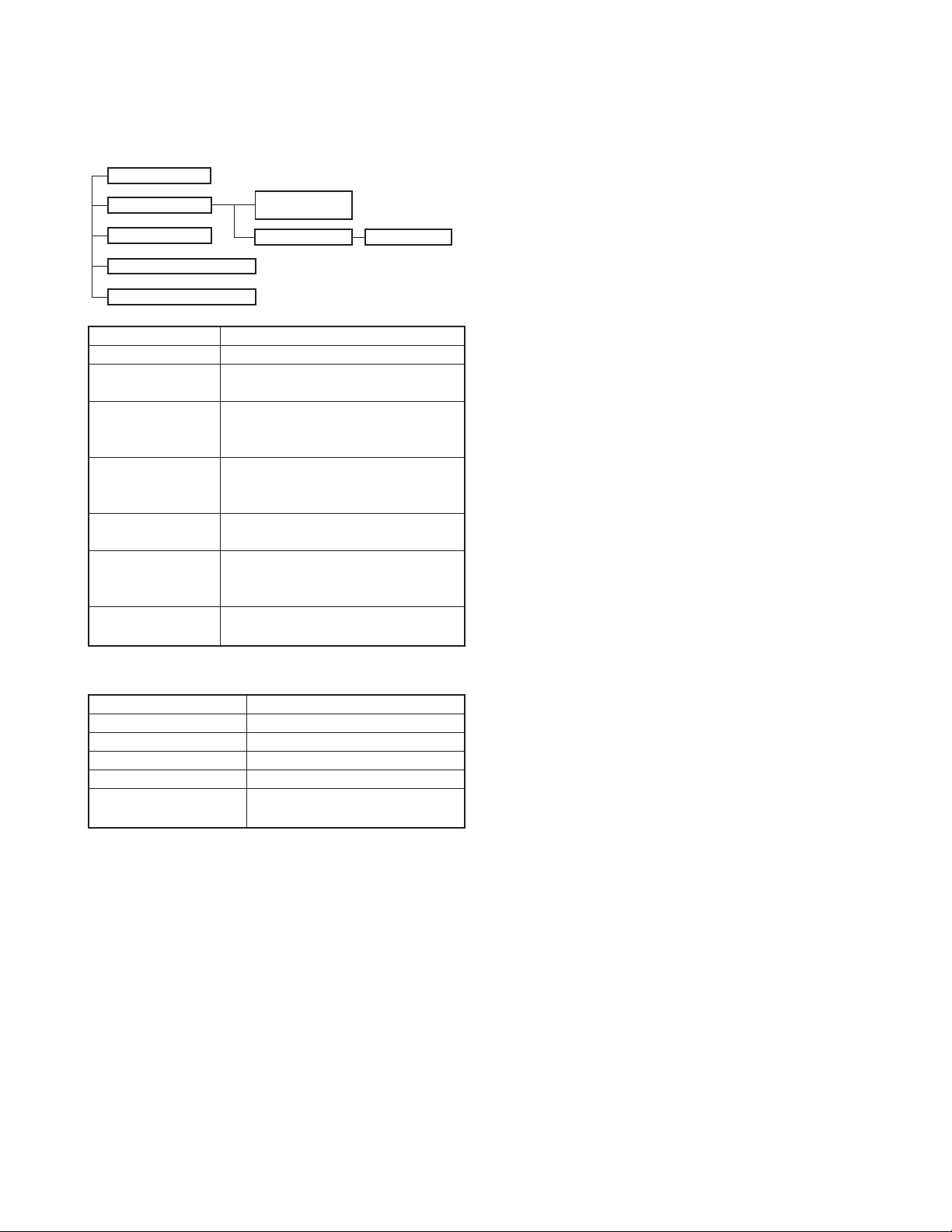
3-1. Preface
The transceiver is programmed using a personal computer,
a programming interface (KPG-22/22A), USB adapter (KCT-53U)
and programming software (KPG-100D).
The programming software can be used with an IBM PC
or compatible. Figure 1 shows the setup of an IBM PC for
programming.
3-2. Connection procedure
1. Connect the transceiver to the personal computer with the
interface cable and USB adapter (When the interface cable
is KPG-22A, the KCT-53U can be used.).
3-4. KCT-53U description (USB adapter : Option)
The KCT-53U is a cable which connects the KPG-22A to a
USB port on a computer.
When using the KCT-53U, install the supplied CD-ROM
(with driver software) in the computer. The KCT-53U driver
runs under Windows 2000 or XP.
3-5. Programming software KPG-100D description
KPG-100D is the programming software for the transceiver
supplied on a CD-ROM. This software runs under Windows
98, ME, Windows 2000 or XP on an IBM-PC or compatible
machine.
The data can be input to or read from the transceiver and
edited on the screen. The programmed or edited data can be
printed out. It is also possible to tune the transceiver.
3
TK-3212L
REALIGNMENT
IBM-PC
KPG-22 or KPG-22A or KPG-22A + KCT-53U
Illustration is KPG-22.
Gray +
Gray/Black –
1.5D-XV Lead wire +
1.5D-XV Shield wire –
PC
USB
KCT-53U
KPG-22A
Transceiver
RF Power meter
or SSG
PC
D-SUB
(25-pin)
KPG-22
Transceiver
KPG-100D
PC
D-SUB
(9-pin)
KPG-22A
Transceiver
Tuning cable
(E30-3216-05)
Fig. 1
4. Clone Mode
4-1. Outline
"Clone Mode" copies the transceiver data to another
transceiver.
The dealer can copy the transceiver data to another
transceiver even without the use of a personal computer.
4-2. Example
The transceiver can copy the programming data to one or
more transceivers via RF communication.
The clone source and clone target/s must be in Clone mode.
4-3. Operation
1. To switch the clone target/s to Clone mode, press and hold
the [<B] key while turning the transceiver power ON.
2. Wait for 2 seconds. “CLONE” appears on the LCD, followed
by “FRQTBL 1”.
3. Select a channel table number using the [Selector] knob.
4. To switch the clone source to Clone mode, press and hold
the [<B] key while turning the transceiver power ON.
5. Wait for 2 seconds. “CLONE” appears on the LCD, followed
by “FRQTBL 1”.
6.
Select the same channel table number as the clone target/s.
7. Press the [S] key on the clone source to begin data
transmission. When the clone target starts to receive data,
the green LED will light and “CLONING” will appear on
the LCD. The source unit will display “MASTER”.
8. When the clone source finishes sending data, a
“confirmation” tone will sound and “COMPLETE” will
appear on the LCD. If data transmission failed while cloning,
the Target unit will produced an error tone and “CLONE
NG” will appear on the LCD.
4
9. If the cloning fails, no data will be available in the Target
unit when it is returned to User mode.
10.When the cloning is successful, the Target unit's "Scan"
and "Key lock" functions will return to their default values
SP
}
MIC
}
(Scan = OFF, Key lock = OFF).
11.
The source will remain in clone mode after cloning. The
target unit will return to user mode after a successful cloning.
Notes:
• The dealer can clone data to two or more transceivers by
repeating the above procedures.
• If the transceivers Clone Mode is configured as "Disabled",
the transceiver cannot enter Clone mode.
• The table shown below will cover the frequency tables used
for wireless cloning.
•Clone mode cannot be entered in battery low state.
•A unit cannot be a "Source Unit" if it is unprogrammed. If
the [S] key is pressed, an "error" tone will sound.
• Once a unit is set to be the Source, it cannot be a target
after the data has been transmitted. This protects the data
in the Source unit.
• MSK signaling is used in cloning.
• Electronic interface may cause a failure in data transfer
during Wireless Clone, such as when waveforms or
electromagnetics are being performed at the workbench.
• Clone mode can be used ONLY by the authorized service
personnel.
• The Clone mode setting must be configured as "Disable"
before being delivered to the end-user.
•
To clone, replace the antenna from both the source
transceiver and the target transceiver with a dummy load.
• The transmit output power is automatically set to Low
in Clone mode.
Cloning Frequency Table
Type K, M K2, M2
Operating Frequency
Clone (MHz)
450~490 470~512
Frequency Table
1 450.000 470.000
2 452.000 472.000
3 454.000 474.000
4 456.000 476.000
5 458.000 478.000
6 460.000 480.000
7 462.000 482.000
8 464.000 484.000
9 466.000 486.000
10 468.000 488.000
11 470.000 490.000
12 472.000 492.000
13 474.000 494.000
14 476.000 496.000
15 478.000 498.000
16 480.000 500.000
17 482.000 502.000
18 484.000 504.000
19 486.000 506.000
20 488.000 508.000
REALIGNMENT
TK-3212L
4-4. Adding the Data Password
If the Data password is set to the transceiver, you must
enter the password to activate a clone mode. The maximum
length of the password is 6 digits.
The following describes how to enter the password.
1. Press and hold the [S] key for 2 seconds while turning the
transceiver power on.
2. “CLN.LOCK.R”(When the Read authorization password is
set to the transceiver.) / “CLN.LOCK.W” (When the
Overwrite password is set to the transceiver.) is displayed
on the LCD.
3. If the [selector] knob is rotated while “CLN.LOCK.R”/
“CLN.LOCK.W” is displayed, the number (0 to 9) flashes
on the LCD.
When you press the [C>] key, the currently selected
number is determined.
If you press the [A] key, the least digit of the password is
deleted.
If you press the [S] key after entering the password in this
procedure, “FRQTBL 1” is displayed if the entered
password is correct.
If the password is incorrect, “CLN.LOCK.R”/
“CLN.LOCK.W” is redisplayed.
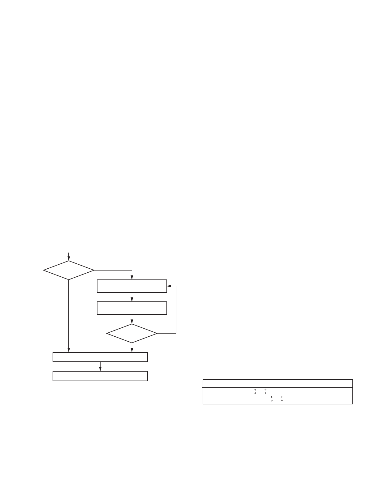
■ Flow Chart (Source transceiver)
[<B]+Power ON
Is Data
password
set?
No
Ye s
"CLN.LOCK.R”/“CLN.LOCK.W”
Clone mode
Start the clone function
is displayed.
Enter the password and
then press the [S] key.
Is password
[S]
correct?
No
Ye s
5. Self Programming Mode
Write mode for frequency data and signaling, etc. To be
used ONLY by the authorized service person maintaining the
user's equipment. After programming, reset the FPU to the
"Self- Programming" disabled mode. Transceivers CANNOT be
delivered to the end-user in the self-programming mode.
5-1. Enter to the Self Programming Mode
Press and hold the [S] key for 2 seconds while turning the
transceiver power on.
When the transceiver enters in the self programming mode,
"1- 1" is displayed 2 seconds after "SELF " is displayed.
Note :
This mode (self programming mode) cannot be set when it
has been disabled with the FPU.
5-2. Adding the Data Password
If the Data password is set to the transceiver, you must
enter the password to activate a self programming mode. The
maximum length of the password is 6 digits.
The following describes how to enter the password.
1. Press and hold the [S] key for 2 seconds while turning the
transceiver power on.
2. "SLF.LOCK.R"(When the Read authorization password is
set to the transceiver.) / "SLF.LOCK.W" (When the
Overwrite password is set to the transceiver.) is displayed
on the LCD.
3. If the [selector] knob is rotated while "SLF.LOCK.R"/
"SLF.LOCK.W" is displayed, the number (0 to 9) flashes on
the LCD.
When you press the [C>] key, the currently selected
number is determined.
If you press the [A] key, the least digit of the password is
deleted.
If you press the [S] key after entering the password in this
procedure, "SELF" is displayed if the entered password is
correct.
If the password is incorrect, "SLF.LOCK.R"/ "SLF.LOCK.W"
is redisplayed.
5-3. Channel Selection Mode
In this mode, the Zone or Channel can be selected.
Press and hold the [S] key for 2 seconds while turning the
transceiver power on to enter self programming mode. When
the transceiver enters in the self programming mode, the
transceiver automatically enters the Channel Selection mode.
2 seconds after displaying "SELF", "1- 1" appears on the LCD.
The setup item for channel selection mode is as follows.
Setup item Display Remarks
Select ∗∗∗ - ∗∗∗ Zone: 1~128
Zone/Channel ∗∗∗ - ∗∗∗ Channel: 1~128
5
TK-3212L
REALIGNMENT
Key operation
Key Key Function
[Selector] Toggle between Zone selection and Channel selection.
[Side1] No action
[Side2] No action
[S] Enter the Item Selection mode
[A] Error tone sounds
[<B] Decrement the blinking Zone/Channel number by 1.
Press and hold to decrement in steps of 10.
[C>] Increment the blinking Zone/Channel number by 1.
Press and hold to decrement in steps of 10.
Note :
If a non-existing Zone-Channel is selected and the memory
for all 128 channels is already filled, an error tone will sound
and "MEM.FULL" will appear on the LCD for 2 seconds.
5-4. Item Selection Mode
In this mode, the following items can be selected.
• RX frequency
• RX signaling
• TX frequency
• TX signaling
•Wide/ Narrow
• RF power Hi/Low
• Scan Del/Add
• Beat shift on/off
• Compander on/off
When the [S] key is pressed in the Channel Selection mode,
the transceiver enters the Item Selection mode.
Key operation
Key Key Function
[Selector] The selected item changes
[Side1] No action
[Side2] No action
[S] Enter the Item Setting mode
[A] Return to the Channel Selection mode
[<B] Error tone sounds
[C>] Error tone sounds
The setup items for item setting mode are as follows.
Setup item Display Remarks
1.RX frequency 1. RX FREQ→Receive frequency
∗∗∗.∗∗∗∗∗
2.RX signaling 2. RX SIG
TONE OFF/
QT ∗∗∗.∗ /
DQT∗∗∗N/
DQT∗∗∗I
3.TX frequency 3. TX FREQ
∗∗∗.∗∗∗∗∗
4.TX signaling 4. T X SIG
TONE OFF/
QT ∗∗∗.∗ /
DQT∗∗∗N/
DQT∗∗∗I
5. Wide / Narrow 5. BAND ∗ W / N
6.
RF power Hi / Low
7.Scan Del / Add 7. SCN ∗∗∗ DEL / ADD
8.Beat shift on / off 8. SFT ∗∗∗ ON / OFF
9.
Compander on / off
6. PWR ∗∗∗ HI / LOW
9. CMP ∗∗∗ ON / OFF
327.00000~550.00000MHz
→
Receive QT/DQT
→
Transmit frequency
327.00000~550.00000MHz
→
Transmit QT/DQT
Key operation
Key Key Function
[Selector] Changing the selection item (RX/ TX frequency and
RX/ TX signaling only)
[Side1] No action
[Side2] No action
[S] • Store the current settings and return to the Item
Selection mode.
•A MHz digit of the frequency blinks.
(RX/ TX frequency only)
• The icon of the current signaling configuration blinks.
(RX/ TX signaling only)
[A] Abort the current settings and return to the Item
Selection mode without backup.
[<B] Toggle/ Decrease the blinking value.
[C>] Toggle/ Increase the blinking value.
5-5. Item Setting Mode
In this mode, the selected item in the Item Selection mode
can be programmed.
When the [S] key is pressed in the Item Selection mode,
the transceiver enters the Item Setting mode.
6
REALIGNMENT
TK-3212L
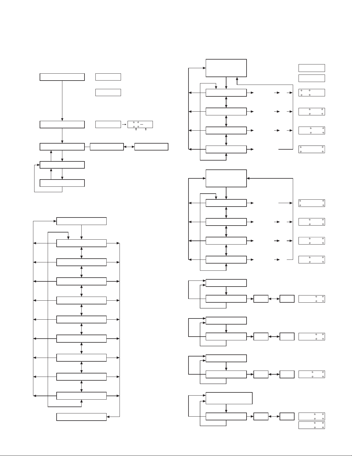
5-6. Self Programming Mode flow chart
■ Channel selection mode flow chart
[S]+Power ON
Data password
Read authorization password /
Overwrite password entry (6 digits)
[S]
Self programming mode SELF
Channel selection mode
[A]
Item selection mode
[A]
Item setting mode
[S]
[S]
[S]
■ Item selection mode flow chart
Channel selection mode
[S]
[A]
[A]
[A]
[A]
[A]
1. RX frequency
2. RX signaling
3. TX frequency
4. TX signaling
5. Wide / Narrow
6. RF power Hi / Low
7. Scan Del / Add
8. Beat shift on / off
9. Compander on / off
Item setting mode
Display
SLF.LOCK.R
SLF.LOCK.W
Zone selection Channel selection
[<B] : Zone/Channel number decrement
[C>] : Zone/Channel number increment
[Selector]
[Selector]
[Selector]
[Selector]
[Selector]
[Selector]
[Selector]
[Selector]
[Selector]
When the Read
authorization password is
set to the transceiver.
or
When the Overwrite
authorization password is
set to the transceiver.
[Selector]
[S]
[S]
[S][A]
[S]
[S][A]
[S]
[S][A]
[S]
[S][A]
11
Zone
Channel
■ Item setting mode flow chart
[1. RX frequency] or
[3. TX frequency]
[S]
[A]
[A]
[A]
[A]
[A]
[A]
[A]
[A]
[A]:Not
stored
[A]:Not
stored
[A]:Not
stored
[A]:Not
stored
MHz setting
[Selector]
KHz setting
[Selector]
Channel step
[Selector]
Frequency clear
[Selector]
[2. RX signaling] or
[4. TX signaling]
[S]
OFF
[Selector]
QT
[Selector]
DQT N
[Selector]
DQT I
[Selector]
5. Wide / Narrow
[S]
Wide / Narrow selection Wide
[S] : Stored
6. RF power Hi / Low
[S]
Hi / Low selection Hi Low
[S] : Stored
7. Scan Del / Add
[S]
Del / Add selection Del Add
[S] : Stored
[8. Beat shift on / off] or
[9. Compander on / off]
[S]
on / off selection on off
[S] : Stored
[<B] / [C>] [S]
[<B] / [C>] [S]
[<B] / [C>] [S]
[S] : Cleared
[S] : Tone off
[<B] / [C>] [S]
[<B] / [C>] [S]
[<B] / [C>] [S]
Current
setting value
Value is not set
[<B] / [C>]
Narrow
[<B] / [C>]
[<B] / [C>]
[<B] / [C>]
Display
450. 00000
--------
450. 00000
450. 00000
STP 5.00K
--------
Display
TONE OFF
67.0QT
023NDQT
023 IDQT
Display
W5.BAND
Display
HI6.PWR
Display
ADD7.SCN
Display
ON8.SFT or
ON9.CMP
7
TK-3212L
REALIGNMENT /
CIRCUIT DESCRIPTION
6. Firmware Version Information
Turn the transceiver ON with the [Side1] and [Side2] keys
held down. Then, the version is displayed during holding the
[Side1] and [Side2] keys.
CIRCUIT DESCRIPTION
1. Control Circuit
The control circuit consists of a microprocessor (IC405) and
its peripheral circuits. It controls the TX-RX unit and transfers
data to the Display unit. IC405 mainly performs the following:
(1) Switching between transmission and reception by the
PTT signal input.
(2) Reading system, group, frequency, and program data
from the memory circuit.
(3) Sending frequency program data to the PLL.
(4) Controlling squelch on/off by the DC voltage from the
squelch circuit.
(5) Controlling the audio mute circuit by the decode data
input.
(6) Transmitting tone and encode data.
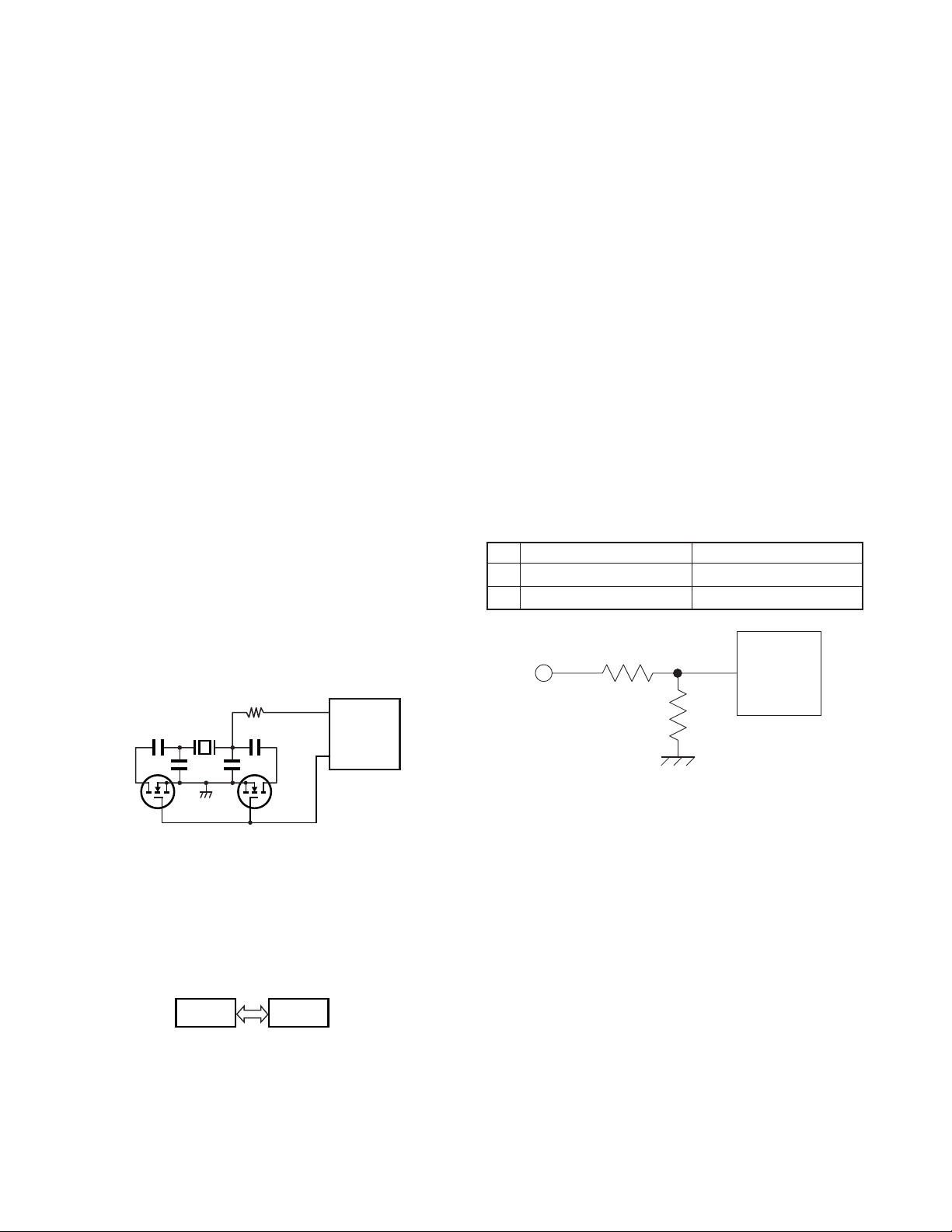
1) Frequency Shift Circuit
The microprocessor (IC405) operates at a clock of
7.3728MHz. This oscillator has a circuit that shifts the
frequency by BEAT SHIFT SW (Q407, Q408).
A beat sound may be able to be evaded from generation if
“Beat Shift” is set to ON when it is generated in the internal
spurious transmission modulated sound of a transceiver.
11
XOUT
X3
8
IC405
BSHIFT
3) Low Battery Warning
The battery voltage is checked by the microprocessor.
The transceiver generates a warning tone when the battery
voltage falls below the warning voltage (2) shown in the
table.
(1) The red LED blinks when the battery voltage falls below
the voltage (1) shown in the table during transmission.
Transmission is still allowed.
Note:
The transceiver checks the battery voltage during reception
even when, in the FPU, the Battery Warning status function
is set to “While Transmitting” (default setting).
However, the LED does not blink during reception. The red
LED blinks during transmission. The transceiver is still
usable.
(2) The transceiver immediately stops transmission when
the battery voltage falls below the voltage (2) shown in
the table. A warning tone sounds while the PTT switch
is pressed.
Ni-MH Battery Li-ion Battery
(1) 6.2V 6.2V
(2) 5.8V 5.8V
SB
R404
88
R406
IC405
BATT
CPU
Q408
H:OFF
L:ON
Q407
H:OFF
L:ON
Fig. 1 Frequency shift circuit
2) Memory Circuit
Memory circuit consists of the CPU (IC405) and an EEPROM
(IC406). An EEPROM has a capacity of 128k bits that
contains the transceiver control program for the CPU and
data such as transceiver channels and operating features.
IC405
CPU
IC406
EEPROM
Fig. 2 Memory circuit
8
Fig. 3 Low battery warning
PARTS LIST
TK-3212L
CAPACITORS
1 = Type ... ceramic, electrolytic, etc.
2 = Shape ... round, square, ect.
3 = Temp. coefficient
Temperature coefficient
1st Word
Color*
ppm/
Tolerance (More than 10pF)
Code
(%)
Voltage rating
1st word
Black Red Orange Yellow Green Blue Violet
0 -80 -150 -220
C
0.25 0.5 2 5 10 20
2nd word
0
1
2
3
CC 45
1
1
2
LCPRSTU
DG J KMX ZP
A
BCD EF
1.0
1.25
10
12.5
100
125
1000
1250
TH 1H J220
3
4
5
4 = Voltage rating
5 = Value
6 = Tolerance
2.0
1.6
20
16
200
160
2000
1600
6
-330 -470 -750
+ 40
+ 80
- 40
- 20
3.15
2.5
31.5
25
315
250
3150
2500
CC45
+ 100
-0
G
4.0
40
400
4000
Color*
2nd Word HG
ppm/
Example : CC45TH = -470
No code
More than 10µF -10 +50
Less than 4.7µF -10 +75
H
J
5.0
6.3
50
63
500
630
5000
6300
Capacitor value
010 = 1pF
100 = 10pF
101 = 100pF
102 = 1000pF = 0.001µF
103 = 0.01µF
30 60
K
V
8.0
-
80
35
800
-
8000
-
22
JKL
120 250 500
60ppm/
(Less than 10pF)
Gode
(pF)
CD FGB
0.1 0.25 0.5 1 2
0 = 22pF
Multiplier
2nd number
1st number
Chip capacitors
(EX) C C 7 3 F S L 1 H
(Chip)(CH,RH,UJ,SL)
(EX) C K 7 3 F F 1 H
(Chip)(B,F)
RESISTORS
Chip resistor (Carbon)
(EX) R D 7 3 E B 2 B
(Chip)(B,F)
Carbon resistor (Normal type)
(EX) R D 1 4 B B
1 = Type
2 = Shape
3 = Dimension
4 = Temp. coefficient
2C
000
000
000
000
J
7654321
Z
7654321
J
7654321
J
7654321
5 = Rating wattage
6 = Value
7 = Tolerance
Refer to the table above.
1 = Type
2 = Shape
3 = Dimension
4 = Temp. coefficient
5 = Voltage rating
6 = Value
7 = Tolerance
Dimension (Chip capacitors)
Dimension code L W T
Empty
A
B
C
D
E
F
G
H
Dimension
Dimension (Chip resistor)
Dimension code L W T
E
F
G
H
Rating wattage
Wattage
Code
1/16W
1J
1/10W
2A
1/8W
2B
W
1.0
Code
2C
2E
2H
5.6
4.5
4.5
4.5
3.2
3.0
2.0
1.6
1.0
L
3.2
2.0
1.6
0.5
0.5
0.5
0.5
0.4
0.2
0.3
0.2
0.05
0.2
0.3
0.2
0.05
Wattage
1/6W
1/4W
1/2W
5.0
3.2
2.0
1.25
2.5
1.6
1.25
0.8
0.5
1.6
1.25
0.8
0.5
Code
0.5
0.4
0.3
0.2
0.3
0.2
0.2
0.2
0.05
T
0.2
0.2
0.2
0.05
3A
3D
Less than 2.0
Less than 2.0
Less than 2.0
Less than 1.25
Less than 1.5
Less than 1.25
Less than 1.25
Less than 1.0
0.5
0.35
Wattage
1W
2W
0.5
0.05
1.0
1.0
0.1
0.05
9
TK-3212L
PARTS LIST
New Parts. indicates safety critical components.
∗
Parts without Parts No. are not supplied.
Les articles non mentionnes dans le Parts No. ne sont pas fournis.
Teile ohne Parts No. werden nicht geliefert.
TK-3212L (Y50-6220-XX)
TX-RX UNIT (X57-7130-XX)
New
Ref. No.
Address
Parts No. Description
parts
TK-3212L
11B∗ A02-3894-43 PLASTIC CABINET ASSY
23A∗ A10-4078-41 CHASSIS
32C B09-0680-03 CAP(SP/MIC) ACCESSORY
42B B11-1817-04 ILLUMINATION GUIDE(TX/RX)
51A B11-1830-03 ILLUMINATION GUIDE(LCD)
61A B38-0906-25 LCD ASSY
71C∗ B62-1996-00 INSTRUCTION MANUAL
91B D10-0649-03 LEVER
10 1B D21-0863-04 SHAFT
11 1B D32-0441-03 STOPPER
12 2A E04-0465-05 RF COAXIAL RECEPTACLE(SMA)
13 3A E23-1253-04 TERMINAL(BATT-)
14 2B E37-1158-05 PROCESSED LEAD WIRE(WHITE:SP+)
15 2B E37-1176-05 PROCESSED LEAD WIRE(GREEN:SP-)
16 3A F20-3353-14 INSULATING SHEET(CHASSIS BATT+)
17 2B G01-4542-04 COIL SPRING(LEVER)
18 2B G01-4543-04 COIL SPRING(STOPPER)
19 2A G10-1330-04 FIBROUS SHEET(IC302:AUDIO IC)
21 2A G10-1348-04 FIBROUS SHEET(SP WIRE)
22 3A G11-4283-04 RUBBER SHEET(Q103:FINAL FET)
23 2A G11-4359-04 SHEET(FPC CONNECTOR)
24 3A G13-2009-04 CUSHION(CHASSIS)
25 3A G13-2033-04 CUSHION(TERMINAL BATT-)
26 3A G13-2034-14 CUSHION(TERMINAL BATT-)
27 3A ∗ G13-2038-24 CUSHION(CHASSIS-CERAMIC FILTER)
28 2A ∗ G13-2039-14 CUSHION(PCB-CERAMIC FILTER)
30 2A G13-2053-04 CUSHION(CHASSIS,ENC)
31 2A G13-2074-04 CUSHION(PCB)
32 3A G13-2088-04 CUSHION(CHASSIS,VOL)
33 2A G13-2107-04 CUSHION(MOUNTING HARDWARE)
34 3A G53-1604-03 PACKING(CHASSIS)
35 3A G53-1605-03 PACKING(TERMINAL BATT+)
36 2B G53-1606-13 PACKING(VOL/ENC/LED)
38 2A G53-1610-04 PACKING(SMA)
39 2B G53-1660-03 PACKING(SP)
40 2A G53-1661-03 PACKING(SP/MIC)
41 2D H12-4221-05 PACKING FIXTURE
43 1C H25-0085-04 PROTECTION BAG (100/200/0.07)
44 3D ∗ H52-2194-02 ITEM CARTON CASE
46 2C J19-5472-03 HOLDER(SP/MIC) ACCESSORY
50 2A J19-5473-03 HOLDER ASSY(TERMINAL BATT+)
51 1A J21-8496-02 MOUNTING HARDWARE(LCD)
52 2B J21-8497-03 MOUNTING HARDWARE(4 KEY)
53 2B J21-8525-03 MOUNTING HARDWARE(VOL/ENC)
54 2D J29-0713-15 BELT CLIP ACCESSORY
56 2A J82-0107-05 FPC
57 1A J99-0385-04 ADHESIVE SHEET(LCD)
59 1B K29-9308-23 BUTTON KNOB(PTT)
60 1B K29-9309-03 KNOB(VOL)
61 1B K29-9345-04 KNOB(ENC)
62 2B K29-9346-02 KEY TOP
63 1B K29-9364-03 BUTTON KNOB(SIDE1/SIDE2)
L:
Scandinavia
Y:
PX (Far East, Hawaii)
Y:
AAFES (Europe)
Destination Destination
Ref. No.
A2B N14-0819-04 CIRCULAR NUT(VOL KNOB)
B2B N14-0832-04 CIRCULAR NUT(CH KNOB)
C2A N30-2604-48 PAN HEAD MACHINE SCREW(SMA)
D3A N30-2606-48
E 1A,2A, N83-2005-48 PAN HEAD TAPTITE SCREW(PCB)
65 2C N99-2046-05 SCREW SET ACCESSORY
66 2A R31-0661-05 VARIABLE RESISTOR(POWER SW/VOL)
67 1B T07-0760-25 SPEAKER
69 3C T90-1039-15 WHIP ANTENNA ACCESSORY K,M
69 3C T90-1040-15 WHIP ANTENNA ACCESSORY K2,M2
71 2A W02-3711-05 ENCODER
72 1D W08-0988-05 CHARGER ACCESSORY
73 1D W08-0989-05 AC ADAPTER (AC120V) ACCESSORY K,K2
73 1D W08-0992-05
Address
2B,3A
K:
New
parts
USA
T:
England
X:
Australia
P:
Canada
E:
Europe
M:
Other Areas
Parts No. Description
PAN HEAD MACHINE SCREW(CHASSIS)
AC ADAPTER (AC220-240V) ACCESSORY
M,M2
TX-RX UNIT (X57-7130-XX) -12:K,M -13:K2,M2
D403 B30-2156-05 LED(RED)
D404 B30-2157-05 LED(YELLOW)
C1 CK73HB1H332K CHIP C 3300PF K
C2 CK73HB1C682K CHIP C 6800PF K
C3 CK73GB1A105K CHIP C 1.0UF K
C4 CK73HB1C103K CHIP C 0.010UF K
C5 CK73HB1H102K CHIP C 1000PF K
C6 CK73HB1A104K CHIP C 0.10UF K
C7 ,8 CC73HCH1H101J CHIP C 100PF J
C9 CC73HCH1H100D CHIP C 10PF D
C10 CS77AA0J100M CHIP TNTL 10UF 6.3WV
C11 CC73HCH1H101J CHIP C 100PF J
C12 CK73HB1H102K CHIP C 1000PF K
C13 CK73HB1A104K CHIP C 0.10UF K
C14 CK73HB1C103K CHIP C 0.010UF K
C15 CC73HCH1H100D CHIP C 10PF D
C16 CK73HB1H102K CHIP C 1000PF K
C17 CC73HCH1H470J CHIP C 47PF J
C18 CC73HCH1H180J CHIP C 18PF J
C19 CK73HB1A104K CHIP C 0.10UF K
C21 CS77AA0J100M CHIP TNTL 10UF 6.3WV
C22 CS77AA1VR33M CHIP TNTL 0.33UF 35WV
C24 CK73HB1H102K CHIP C 1000PF K
C25 CC73HCH1H020B CHIP C 2.0PF B
C26 CC73HCH1H300J CHIP C 30PF J
C27 CS77CA1C3R3M CHIP TNTL 3.3UF 16WV
C29 CK73HB1H471K CHIP C 470PF K
C32 CS77CA1V0R1M CHIP TNTL 0.1UF 35WV
C33 ,34 CK73HB1H102K CHIP C 1000PF K
C35 CC73HCH1H270J CHIP C 27PF J
C38 CC73HCH1H050B CHIP C 5.0PF B
C39 CK73GB1H332K CHIP C 3300PF K
C40 CC73HCH1H030B CHIP C 3.0PF B
C41 CK73GB1H682K CHIP C 6800PF K
C42 CC73HCH1H050B CHIP C 5.0PF B
C43 CC73HCH1H100C CHIP C 10PF C
C44 CK73HB1H471K CHIP C 470PF K
10
Ref. No. Parts No. Description
C45 CK73GB1A105K CHIP C 1.0UF K
C47 CC73HCH1H101J CHIP C 100PF J
C48 CK73HB1H471K CHIP C 470PF K
C49 CC73HCH1H101J CHIP C 100PF J
C50 CC73HCH1H100D CHIP C 10PF D
Address
New
parts
PARTS LIST
Destination
Ref. No. Parts No. Description
C136 CK73GB1A105K CHIP C 1.0UF K
C138 CK73GB1H102K CHIP C 1000PF K
C140 CC73GCH1H101J CHIP C 100PF J
C145 CC73GCH1H160J CHIP C 16PF J K,M
C145 CC73GCH1H180J CHIP C 18PF J K2,M2
Address
New
parts
TK-3212L
TX-RX UNIT (X57-7130-XX)
Destination
C52 CC73HCH1H110J CHIP C 11PF J K,M
C52 CC73HCH1H120J CHIP C 12PF J K2,M2
C54 CC73HCH1H090B CHIP C 9.0PF B
C55 CC73HCH1H110J CHIP C 11PF J K,M
C55 CC73HCH1H120J CHIP C 12PF J K2,M2
C56 CC73HCH1H020B CHIP C 2.0PF B K,M
C58 CC73HCH1H060B CHIP C 6.0PF B K,M
C58 CC73HCH1H090B CHIP C 9.0PF B K2,M2
C59 ,60 CC73HCH1H010B CHIP C 1.0PF B
C61 CC73HCH1H030B CHIP C 3.0PF B K,M
C61 CC73HCH1H040B CHIP C 4.0PF B K2,M2
C62 CC73HCH1H020B CHIP C 2.0PF B
C63 CC73HCH1H101J CHIP C 100PF J
C64 CC73HCH1H040B CHIP C 4.0PF B K,M
C64 ,65 CC73HCH1H050B CHIP C 5.0PF B K2,M2
C65 ,66 CC73HCH1H060B CHIP C 6.0PF B K,M
C66 CC73HCH1H060B CHIP C 6.0PF B K2,M2
C67 CC73HCH1H050B CHIP C 5.0PF B K,M
C67 CC73HCH1H070B CHIP C 7.0PF B K2,M2
C68 -70 CK73HB1H471K CHIP C 470PF K
C71 ,72 CK73HB1A104K CHIP C 0.10UF K
C73 ,74 CC73HCH1H0R5B CHIP C 0.5PF B
C75 ,76 CK73HB1H102K CHIP C 1000PF K
C77 CK73HB1H471K CHIP C 470PF K
C78 CC73HCH1H330J CHIP C 33PF J
C79 CS77CP0J100M CHIP TNTL 10UF 6.3WV
C80 CK73HB1H471K CHIP C 470PF K
C83 CC73HCH1H150J CHIP C 15PF J
C84 -86 CK73HB1H102K CHIP C 1000PF K
C87 CC73HCH1H100D CHIP C 10PF D
C146 CK73GB1H102K CHIP C 1000PF K
C148 CK73GB1H102K CHIP C 1000PF K
C151 CC73GCH1H070B CHIP C 7.0PF B K2,M2
C152 CC73GCH1H200J CHIP C 20PF J
C154 CK73GB1H471K CHIP C 470PF K
C156 CC73GCH1H060B CHIP C 6.0PF B K,M
C156 CC73GCH1H3R5B CHIP C 3.5PF B K2,M2
C157 CC73GCH1H040B CHIP C 4.0PF B K2,M2
C157 CC73GCH1H2R5B CHIP C 2.5PF B K,M
C158 CC73GCH1H101J CHIP C 100PF J
C159 CC73GCH1H020C CHIP C 2.0PF C K,M
C159 CC73GCH1H030B CHIP C 3.0PF B K2,M2
C160 CC73GCH1H020B CHIP C 2.0PF B K,M
C160 CC73GCH1H1R5B CHIP C 1.5PF B K2,M2
C161 CC73GCH1H050B CHIP C 5.0PF B K,M
C161 CC73GCH1H060B CHIP C 6.0PF B K2,M2
C163 CC73GCH1H030B CHIP C 3.0PF B
C164 CC73GCH1H050B CHIP C 5.0PF B K,M
C164 CC73GCH1H060B CHIP C 6.0PF B K2,M2
C166 CC73GCH1HR75B CHIP C 0.75PF B K,M
C166 CC73GCH1H1R5B CHIP C 1.5PF B K2,M2
C168 CC73GCH1H0R3B CHIP C 0.3PF B K2,M2
C168 CC73GCH1H010B CHIP C 1.0PF B K,M
C169 CC73GCH1H050B CHIP C 5.0PF B K,M
C169 CC73GCH1H090B CHIP C 9.0PF B K2,M2
C190 CK73GB1A105K CHIP C 1.0UF K
C191 CK73GB1H103K CHIP C 0.010UF K
C201 CK73GB1A224K CHIP C 0.22UF K
C206 CK73HB1H102K CHIP C 1000PF K
C207 CK73HB1H182K CHIP C 1800PF K
C90 CK73HB1H102K CHIP C 1000PF K
C100 CK73HB1H471K CHIP C 470PF K
C101 CK73GB1H471K CHIP C 470PF K
C102 CC73GCH1H120J CHIP C 12PF J
C106 CK73HB1H471K CHIP C 470PF K
C107 CC73GCH1H060B CHIP C 6.0PF B
C108 CK73HB1H471K CHIP C 470PF K
C110,111 CK73GB1H471K CHIP C 470PF K
C112 CC73GCH1H070D CHIP C 7.0PF D
C113 CK73GB1C104K CHIP C 0.10UF K
C116 CC73GCH1H110J CHIP C 11PF J
C119 CK73GB1H471K CHIP C 470PF K
C122 CC73GCH1H330J CHIP C 33PF J
C123 CC73GCH1H330G CHIP C 33PF G
C124 CC73HCH1H100D CHIP C 10PF D
C125 CC73GCH1H060B CHIP C 6.0PF B
C126 CS77CA1C010M CHIP TNTL 1.0UF 16WV
C127 CC73GCH1H200J CHIP C 20PF J
C128 CK73HB1H471K CHIP C 470PF K
C129 CK73GB1H471K CHIP C 470PF K
C130 CK73HB1H471K CHIP C 470PF K
C132 CC73GCH1H270J CHIP C 27PF J
C133 CK73GB1H471K CHIP C 470PF K
C134 CK73GB1H103K CHIP C 0.010UF K
C135 CK73GB1C104K CHIP C 0.10UF K
C208 CK73HB1H471K CHIP C 470PF K
C209 CS77CP0J100M CHIP TNTL 10UF 6.3WV
C210 CK73HB1H471K CHIP C 470PF K
C211 CK73HB1C103K CHIP C 0.010UF K
C213 CK73HB1A104K CHIP C 0.10UF K
C214 CC73HCH1H680J CHIP C 68PF J
C215 CK73HB1H102K CHIP C 1000PF K
C216 CK73GB1C104K CHIP C 0.10UF K
C217 CK73HB1A104K CHIP C 0.10UF K
C218 CK73GB1C104K CHIP C 0.10UF K
C219 CC73HCH1H330J CHIP C 33PF J
C220 CK73HB1H102K CHIP C 1000PF K
C221 CK73GB1C104K CHIP C 0.10UF K
C222 CK73HB1H102K CHIP C 1000PF K
C224,225 CK73HB1C103K CHIP C 0.010UF K
C228 CC73GCH1H100C CHIP C 10PF C
C230 CK73HB1C103K CHIP C 0.010UF K
C231 CK73GB1H103K CHIP C 0.010UF K
C232 CK73HB1C103K CHIP C 0.010UF K
C233 CC73GCH1H060B CHIP C 6.0PF B
C234 CK73HB1H102K CHIP C 1000PF K
C236 CC73GCH1H180J CHIP C 18PF J
C237 CK73HB1H102K CHIP C 1000PF K
C238 CK73GB1C104K CHIP C 0.10UF K
C239 CK73GB1H102K CHIP C 1000PF K
11

TK-3212L
TX-RX UNIT (X57-7130-XX)
Ref. No. Parts No. Description
C240 CC73GCH1H3R5B CHIP C 3.5PF B
C241 CK73GB1H471K CHIP C 470PF K
C244 CC73GCH1H030B CHIP C 3.0PF B K,M
C245 CC73GCH1H220J CHIP C 22PF J K,M
C246 CC73GCH1H010B CHIP C 1.0PF B K,M
Address
New
parts
PARTS LIST
Destination
Ref. No. Parts No. Description
C321 CK73GB1C473K CHIP C 0.047UF K
C322 CK73HB1C153K CHIP C 0.015UF K
C323 CC73GCH1H820J CHIP C 82PF J
C324 CC73HCH1H820J CHIP C 82PF J
C325 CK73HB1A104K CHIP C 0.10UF K
Address
New
parts
Destination
C247 CK73HB1H471K CHIP C 470PF K K,M
C248 CC73GCH1H020B CHIP C 2.0PF B K,M
C249 CC73GCH1H030B CHIP C 3.0PF B K2,M2
C249 CC73GCH1H050B CHIP C 5.0PF B K,M
C250 CC73GCH1H180J CHIP C 18PF J K2,M2
C250 CC73GCH1H220J CHIP C 22PF J K,M
C251 CK73HB1H471K CHIP C 470PF K
C252 CC73GCH1H1R5B CHIP C 1.5PF B K2,M2
C252,253 CC73GCH1H020B CHIP C 2.0PF B K,M
C253 CC73GCH1H010B CHIP C 1.0PF B K2,M2
C254 CK73HB1H471K CHIP C 470PF K
C255 CC73GCH1H180J CHIP C 18PF J K2,M2
C255 CC73GCH1H220J CHIP C 22PF J K,M
C256 CS77CP0J4R7M CHIP TNTL 4.7UF 6.3WV
C257 CC73GCH1H050B CHIP C 5.0PF B K2,M2
C257 CC73GCH1H3R5B CHIP C 3.5PF B K,M
C258 CK73HB1H471K CHIP C 470PF K
C259 CK73GB1H471K CHIP C 470PF K
C262,263 CK73HB1H471K CHIP C 470PF K
C265 CK73HB1H471K CHIP C 470PF K
C266 CK73GB1H471K CHIP C 470PF K
C267 CC73GCH1H3R5B CHIP C 3.5PF B K,M
C267 CC73GCH1H4R5B CHIP C 4.5PF B K2,M2
C268 CC73GCH1H180J CHIP C 18PF J K2,M2
C268 CC73GCH1H220J CHIP C 22PF J K,M
C269 CC73GCH1H020B CHIP C 2.0PF B
C270,271 CK73HB1H471K CHIP C 470PF K
C272 CC73GCH1H020B CHIP C 2.0PF B
C273 CC73GCH1H180J CHIP C 18PF J K2,M2
C273 CC73GCH1H220J CHIP C 22PF J K,M
C326 CK73HB1H102K CHIP C 1000PF K
C327 CC73HCH1H101J CHIP C 100PF J
C328 CK73HB1H391K CHIP C 390PF K
C329,330 CK73GB1A105K CHIP C 1.0UF K
C331 CK73HB1A104K CHIP C 0.10UF K
C332 CK73HB1H471K CHIP C 470PF K
C333,334 CK73GB1C104K CHIP C 0.10UF K
C335 CC73GCH1H221J CHIP C 220PF J
C336 CK73FB1C474K CHIP C 0.47UF K
C338 CC73GCH1H101J CHIP C 100PF J
C339 CS77AA0J100M CHIP TNTL 10UF 6.3WV
C340 CK73GB1C104K CHIP C 0.10UF K
C341 CK73GB1C473K CHIP C 0.047UF K
C342 CS77AA0J100M CHIP TNTL 10UF 6.3WV
C343 CK73GB1C473J CHIP C 0.047UF J
C344 CC73GCH1H221J CHIP C 220PF J
C345 CS77AB20J101M CHIP TNTL 100UF 6.3WV
C346 CK73GB1H102K CHIP C 1000PF K
C348 CK73HB1H471K CHIP C 470PF K
C350 CK73HB1H471K CHIP C 470PF K
C351,352 CK73HB1C103K CHIP C 0.010UF K
C354 CK73HB1A104K CHIP C 0.10UF K
C356 CK73HB1A333K CHIP C 0.033UF K
C357 CK73HB1E472K CHIP C 4700PF K
C401 CC73GCH1H471J CHIP C 470PF J
C402 CK73HB1H102K CHIP C 1000PF K
C403 CK73GB1C104K CHIP C 0.10UF K
C405 CC73GCH1H101J CHIP C 100PF J
C406 CK73HB1E472K CHIP C 4700PF K
C407 CK73HB1H102K CHIP C 1000PF K
C274 CC73GCH1H1R5B CHIP C 1.5PF B K2,M2
C274,275 CC73GCH1H020B CHIP C 2.0PF B K,M
C275 CC73GCH1H2R5B CHIP C 2.5PF B K2,M2
C276 CC73GCH1H020B CHIP C 2.0PF B K2,M2
C276 CC73GCH1H2R5B CHIP C 2.5PF B K,M
C290 CC73GCH1H020B CHIP C 2.0PF B
C291 CC73GCH1H060B CHIP C 6.0PF B
C292 CK73HB1H471K CHIP C 470PF K
C301 CK73HB1H392K CHIP C 3900PF K
C302 CK73HB1H271K CHIP C 270PF K
C304 CK73GB1A224K CHIP C 0.22UF K
C306 CS77AA0J4R7M CHIP TNTL 4.7UF 6.3WV
C307,308 CK73HB1A104K CHIP C 0.10UF K
C309 CC73GCH1H820J CHIP C 82PF J
C310 CK73HB1A683K CHIP C 0.068UF K
C311 CK73GB1A105K CHIP C 1.0UF K
C312 CC73GCH1H120J CHIP C 12PF J
C313 CC73GCH1H121J CHIP C 120PF J
C314 CK73HB1A104K CHIP C 0.10UF K
C315 CK73GB1A105K CHIP C 1.0UF K
C316 CK73GB1C104K CHIP C 0.10UF K
C317 CK73HB1A104K CHIP C 0.10UF K
C318 CS77AA0J4R7M CHIP TNTL 4.7UF 6.3WV
C319 CC73GCH1H271J CHIP C 270PF J
C320 CK73HB1C103K CHIP C 0.010UF K
12
C408 CK73HB1E472K CHIP C 4700PF K
C409,410 CK73GB1A105K CHIP C 1.0UF K
C411 CK73HB1H102K CHIP C 1000PF K
C415 CK73HB1H471K CHIP C 470PF K
C417 CK73GB1A105K CHIP C 1.0UF K
C418 CK73HB1E562K CHIP C 5600PF K
C419 CK73HB1H102K CHIP C 1000PF K
C421 CK73GB1A105K CHIP C 1.0UF K
C424 CK73HB1H471K CHIP C 470PF K
C426,427 CK73GB1A105K CHIP C 1.0UF K
C428,429 CK73HB1H102K CHIP C 1000PF K
C430 CK73GB1H103K CHIP C 0.010UF K
C431 CK73HB1C103K CHIP C 0.010UF K
C432 CC73HCH1H050B CHIP C 5.0PF B
C433,434 CC73HCH1H030B CHIP C 3.0PF B
C435 CC73HCH1H050B CHIP C 5.0PF B
C440 CC73GCH1H1R5B CHIP C 1.5PF B
C443 CK73GB1A474K CHIP C 0.47UF K
C444,445 CC73GCH1H070B CHIP C 7.0PF B K,M
C445 CC73GCH1H200J CHIP C 20PF J K2,M2
C450,451 CK73HB1C103K CHIP C 0.010UF K
C452 CK73HB1H102K CHIP C 1000PF K
C456 CK73GB1C104K CHIP C 0.10UF K
C457,458 CK73HB1H471K CHIP C 470PF K K2,M2
C901,902 CK73GB1A105K CHIP C 1.0UF K
 Loading...