

UHF FM TRANSCEIVER / UHF
调频手持对讲机
TK-3178(L
SERVICE MANUAL /
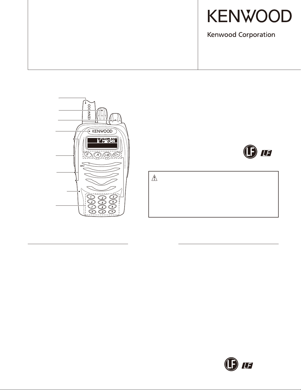
Helical antenna
(T90-1032-55)
Knob (Selector)
(K29-9340-13)
Knob (Volume)
(K29-9278-23)
Badge
(B43-1178-14)
Knob (PTT)
(K29-9447-03)
Key top (Side)
(K29-9341-03)
)
维修手册
无铅焊接通信产品
保护环境建伍领先
© 2009-10 PRINTED IN JA PAN
B51-8888-00 (N) 55
注意∶本产品是无铅化焊接产品
Plastic cabinet assy
(A02-4090-13)
Packing
(G53-1836-01)
CONTENTS
GENERAL .....................................................3
SYSTEM SET-UP .........................................4
REALIGNMENT ...........................................4
DISASSEMBLY FOR REPAIR ......................9
CIRCUIT DESCRIPTION ............................12
SEMICONDUCTOR DATA .........................21
COMPONENTS DESCRIPTION .................24
PARTS LIST ...............................................27
在维修时请使用无铅焊锡
和相应的焊接工具
详细事项请访问如下网址了解:
ADJUSTMENT ..........................................38
TERMINAL FUNCTION .............................54
PC BOARD
TX-RX UNIT (X57-7013-06) (A/4)
TX-RX UNIT (X57-7013-06) (B,C,D/4)
SCHEMATIC DIAGRAM ............................62
BLOCK DIAGRAM .....................................70
LEVEL DIAGRAM ......................................72
http://www.kenwoodhk.com.hk/
............ 56
.....58
EXPLODED VIEW ......................................36
PACKING ....................................................37
This product complies with the
directive for the European market.
RoHS
SPECIFICATIONS ......................................73
This product uses Lead Free solder.

TK-3178(L
)
目 录
概 述 ........................................................................ 3
系统体系 ........................................................................ 4
模式组合 ........................................................................ 4
维修拆卸 ........................................................................ 9
电路说明 ......................................................................12
半导体数据 .................................................................21
元件说明 ......................................................................24
零 件 表 ......................................................................27
部件分解图 .................................................................36
包 装 ......................................................................37
调 整 ......................................................................39
端子功能 ......................................................................55
PC 板
TX-RX 单元 (X57-7013-06)(A/4) ............56
TX-RX 单元 (X57-7013-06)(B,C,D/4) ...58
原 理 图 ......................................................................62
方 块 图 ......................................................................70
电 平 图 ......................................................................72
规 格 ................................................................. 封底
Document Copyrights
Copyright 2009 by Kenwood Corporation. All rights re-
served.
No part of this manual may be reproduced, translated,
distributed, or transmitted in any form or by any means,
electronic, mechanical, photocopying, recording, or otherwise, for any purpose without the prior written permission
of Kenwood.
Disclaimer
While every precaution has been taken in the preparation
of this manual, Kenwood assumes no responsibility for errors or omissions. Neither is any liability assumed for damages resulting from the use of the information contained
herein. Kenwood reserves the right to make changes to any
products herein at any time for improvement purposes.
2
文档版权信息
Kenwood Corporation 拥有版权 2009。保留所有权利。
未经 Kenwood公司预先书面同意,无论出于何种目的,均
不得以任何形式或任何方式包括电子、机械、影印、录音或
其他方式复制、翻译、分发或传播本手册的任何部分。
免责声明
Kenwood 公司在准备本文档时已采取所有必要的预防措施,
恕不对错误或疏漏承担任何责任,也不对因使用本文中所含
的信息而导致的损害负责。Kenwood 公司保留出于改进的需要
而随时对文中的产品信息做出更改的权利。

TK-3178(L
)
GENERAL /
INTRODUCTION
SCOPE OF THIS MANUAL
This manual is intended for use by experienced tech ni cians familiar with similar types of commercial grade com mu ni ca tions equipment. It contains all required service
in for ma tion for the equipment and is current as of the publication date. Changes which may occur after publication
are covered by either Service Bulletins or Manual Revisions.
These are is sued as required.
ORDERING REPLACEMENT PARTS
When ordering replacement parts or equipment in for ma tion, the full part identifi cation number should be in clud ed.
This applies to all parts : components, kits, or chassis. If the
part number is not known, include the chassis or kit number
of which it is a part, and a suffi cient description of the re quired component for proper identifi cation.
PERSONAL SAFETY
The following precautions are recommended for personal
safety:
• DO NOT transmit until all RF connectors are verifi ed se -
cure and any open connectors are properly terminated.
• SHUT OFF and DO NOT operate this equipment near
elec tri cal blasting caps or in an explosive atmosphere.
• This equipment should be serviced by a qualifi ed tech ni -
cian only.
概述
引言
本手册的范围
本手册是提供给熟悉通信专业并且具有维修经验的技术人
员使用的。它包括了维修该设备所需要的全部资料和现行出
版日期。在出版后可能发生变动,如果需要,可以参照《维
修通报》或《手册修订本》进行补充。
替换零件的订购
当订购替换零件或设备资料时,应注意完整的零件识别号
码。所有的零件均有识别号码∶元件,组件或机壳。如果不
知道零件的号码,为了正确地识别,必须注明此元件所属的
机壳或组件的号码,并对元件进行充分的说明。
个人安全
为了个人的安全,请注意下列事项∶
• 在没有认真核实所有射频插头之前或有任何一个脱开的插
头没有连接到相应端口上的情况下均不要发射。
• 在电爆管附近或在易燃性气体环境中,必须关闭电源,不
要操作本设备。
• 本设备只应该由有资格的技术人员进行维修。
SERVICE
This transceiver is designed for easy servicing. Refer to
the sche mat ic diagrams, printed circuit board views, and
align ment procedures contained within.
维修服务
为了便于维修本设备,建立了完整的维修服务体系,提供
了包括原理图,印刷电路板图和调整步骤在内的资料供参考。
3
TK-3178(L
)
SYSTEM SET-UP /
Merchandise received
接收订单
Choose the type of transceiver
选择手持对讲机的类型
Transceiver programming
手持对讲机编程
Are you using the speaker microphone?
您使用扬声器话筒吗?
NO / 否
Delivery
交货
系统体系
Frequency range (MHz) RF power Type
频率范围 (MHz)
TX/RX 350~390
A personal computer, programming interface (KPG-22/22A), and
programming software (KPG-127D) are required for programming.
(The frequency, TX power HI/LOW, and signaling data are
programmed for the transceiver.)
编程时需要个人计算机,编程接口 (KPG-22/22A)和编程软件 (KPG-127D)。
(为手持对讲机设定频率,常规系统特性,TX高/低功率,以及信令数据。)
YES / 是
KMC-17 or KMC-21
Speaker microphone / 扬声器话筒
射频功率
4W
(Option)
(可选件)
类型
TK-3178(L) C6
REALIGNMENT /
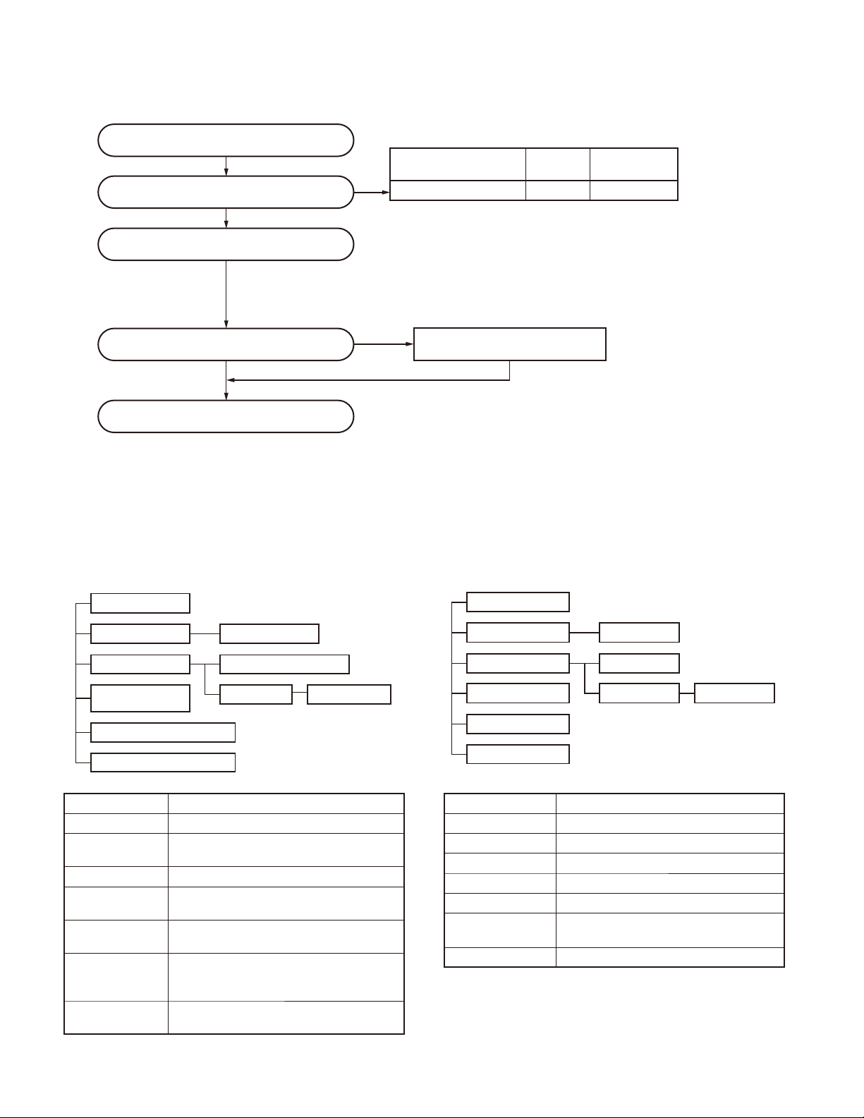
1. Modes
User mode
Panel test mode
PC mode
Firmware
programming mode
Transceiver information mode
Firmware version information
Mode Function
User mode For normal use.
Panel test mode
Panel tuning mode Used by the dealer to tune the transceiver.
PC mode
Data programming
mode
PC test mode
Firmware programming mode
Used by the dealer to check the fundamental
characteristics.
Used for communication between the transceiver and PC.
Used to read and write frequency data and
other features to and from the transceiver.
Used to check the transceiver using the PC.
This feature is included in the FPU.
See panel tuning.
Used when changing the main program of
the fl ash memory.
Panel tuning mode
Data programming mode
PC test mode
PC tuning mode
模式组合
1. 模式
用户模式
面板测试模式
计算机模式
固件编程模式
手持对讲机信息模式
固件版本信息
模 式 功 能
用户模式 一般使用。
面板测试模式 用于经销商检查基本功能。
面板调谐模式 用于经销商调整手持对讲机指标。
计算机模式 用于手持对讲机与计算机之间的通信。
数据编程模式 用于阅读和写入频率数据以及其他功能。
计算机测试模式
固件编程模式 当改变闪存中操作主程序时使用。
用于使用计算机检测。此特性包括在 FPU
内。参见面板调谐。
面板调谐模式
数据编程模式
计算机测试模式
计算机调谐模式
4
TK-3178(L
)
REALIGNMENT /
Mode Function
Transceiver information mode
Firmware version
information
2. How to Enter Each Mode
Mode Operation
User mode Power ON
Panel test mode [A] + Power ON
PC mode Received commands from PC
Panel tuning mode [Panel test mode] + [S]
Firmware programming mode [Side2] + Power ON
Transceiver information mode [B] + Power ON
Firmware version information [Side1] + Power ON
3. Panel Test Mode
Setting method refer to ADJUSTMENT.
Used to confi rm the MPT ESN, fi rmware version and transceiver serial number.
Used to confi rm the internal fi rmware version.
模式组合
模 式 功 能
手持对讲机信息模式用于确认 MPT ESN、固件版本和手持对讲
机序列号。
固件版本信息 用于确认内部固件版本。
2. 如何进入每一种模式
模 式 操 作
用户模式 接通电源
面板测试模式 [A]+ 接通电源
计算机模式 从计算机接收指令
面板调谐模式 [ 面板测试模式 ]+[S]
固件编程模式 [Side2]+ 接通电源
手持对讲机信息模式 [B]+ 接通电源
固件版本信息 [Side1]+ 接通电源
3. 关于面板测试模式
关于设定方式,参见调整。
4. Panel Tuning Mode
Setting method refer to ADJUSTMENT.
5. PC Mode
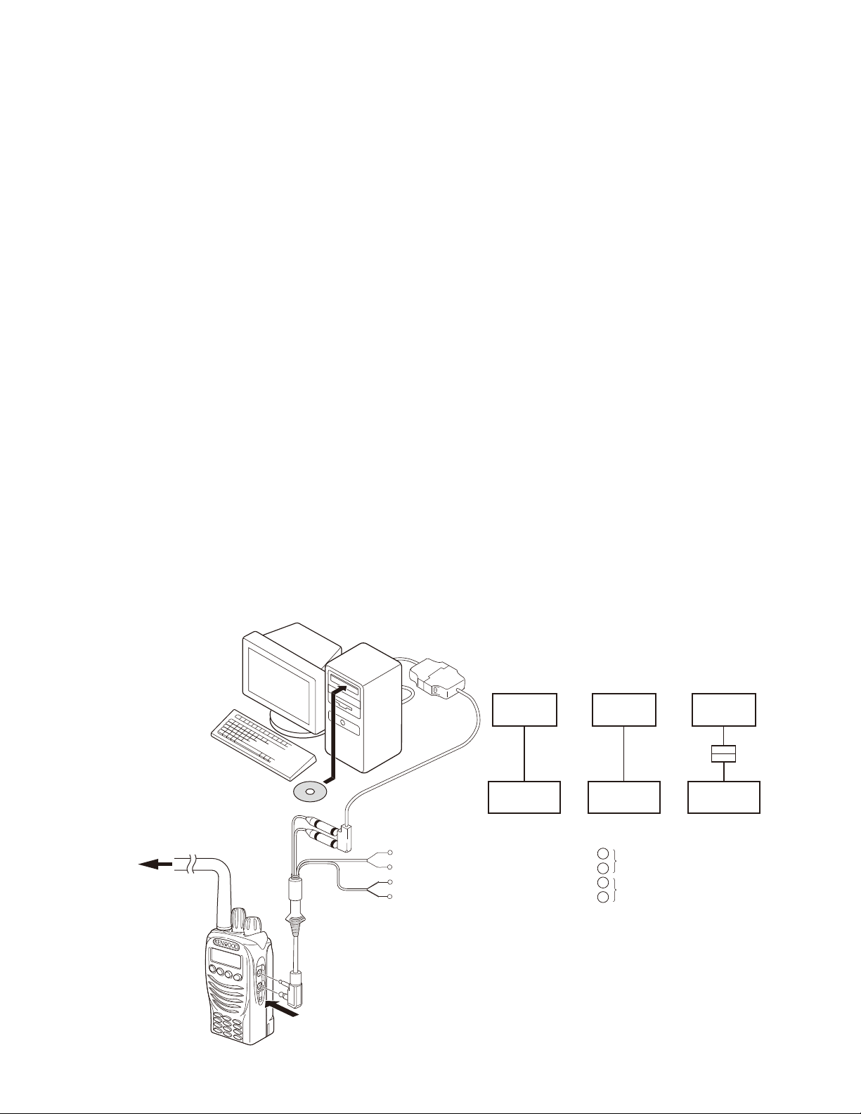
5-1. Preface
The transceiver is programmed by using a personal computer, a programming interface (KPG-22/22A, USB adapter
(KCT-53U)) and FPU (programming software).
The programming software can be used with a PC or
compatible. Figure 1 shows the setup of a PC for programming.
5-2. Connection Procedure
1. Connect the transceiver to the personal computer with
the interface cable and USB adapter (when the interface
cable is KPG-22A, the KCT-53U can be used).
Note:
• You must install the KCT-53U driver in the computer to
use the USB adapter (KCT-53U).
• When using the USB adapter (KCT-53U) for the fi rst time,
plug the KCT-53U into a USB port on the computer with
the computer power ON.
2. When the POWER is switched on, user mode can be en-
tered immediately. When the PC sends a command, the
transceiver enters PC mode.
When data is read from the transceiver, the red LED
lights.
When data is written to by the transceiver, the green LED
lights.
4. 关于面板调谐模式
关于设定方式,参见调整。
5. PC 模式
5-1. 前言
手持对讲机采用个人电脑、编程接口 (KPG-22/22A,USB 适
配器 (KCT-53U)) 和 FPU( 编程软件 ) 进行编程。
编程软件可以在 P C 或兼容的 P C 上进行使用。图 1 给出了
PC 进行编程的设置。
5-2. 连接操作
1. 使用接口电缆和 U S B 适配器将手持对讲机连接到个人电脑
( 接口电缆为 KPG-22A 时,可以使用 KCT-53U)。
注意 :
• 必须在电脑上安装 K C T -53U 驱动程序才能使用 U S B 适配器
(KCT-53U)。
• 首次使用 US B 适配器 (KCT-53U ) 时,请在电脑开机的情况
下将 KCT-53U 插入电脑的 USB 端口。
2. 手持对讲机电源打开时,可以立即进入用户模式。P C 发送
指令时,手持对讲机进入 PC 模式。
手持对讲机发送数据时,红色的 LED 点亮。
手持对讲机接收数据时,绿色的 LED 点亮。
5
TK-3178(L
)
REALIGNMENT /
Note:
• The data stored in the personal computer must match
Model Name and Model Type when it is written into EEPROM.
• Do not press the [PTT] key during data transmission or
reception.
5-3. KPG-22/KPG-22A Description
(PC programming interface cable : Option)
The KPG-22/22A is required to interface the transceiver
with the computer. It has a circuit in its D-sub connector
(KPG-22: 25-pin, KPG-22A: 9-pin) case that converts the RS232C logic level to the TTL level.
The KPG-22/22A connects the SP/MIC connector of the
transceiver to the RS-232C serial port of the computer.
5-4. KCT-53U Description (USB adapter : Option)
The KCT-53U is a cable which connects the KPG-22A to a
USB port on a computer.
When using the KCT-53U, install the supplied CD-ROM
(with driver software) in the computer. The KCT-53U driver
runs under Windows 2000, XP or Vista (32-bit).
模式组合
注意 :
• 个人电脑保存的数据写入 EEPROM 时,必须与机型和类型相
符。
• 请勿在数据发送或接收期间按 [PTT] 键。
5-3. KPG-22/KPG-22A 说明
(PC 编程接口电缆 :选购件 )
将手持对讲机与电脑相连需要 KPG-22/22A。该电缆的
D-sub 连接器 (KPG-22 :25 针,KPG-22A :9 针 ) 盒具有将 RS232C 逻辑电平转换为 TTL 电平的电路。
KP G -22/22A 将手持对讲机的 SP/MIC 连接器连接到电脑的
RS-232C 串行端口。
5-4. KCT-53U 说明 (USB 适配器 :选购件 )
KCT-53U 是将 KPG-22A 连接到电脑 USB 端口的电缆。
使用 K C T -53U 时,请在电脑上安装附带的 CD-ROM( 带有
驱动程序软件 )。KC T -53U 驱动程序在 Windows 2000, X P 或
Vista(32 位 ) 下运行。
5-5. Programming Software KPG-127D Description
The KPG-127D is the programming software for the transceiver supplied on a CD-ROM. This software runs under
Windows 2000, XP or Vista (32-bit) on a PC.
The data can be input to or read from the transceiver and
edited on the screen. The programmed or edited data can
be printed out. It is also possible to tune the transceiver.
PC
KPG-127D
RF Power meter
or SSG
RF功率表或SSG
5-5. 编程软件说明
K P G -127D 是 CD-ROM 附带的用于手持对讲机的编程软件。
该软件在 PC 的 MS-Windows 2000、XP 或 Vista(32 位 ) 下运行。
可在手持对讲机上写入或读取数据,并可在电脑屏幕上进
行编辑。可以打印编程或编辑的数据。此外,还可调谐手持
对讲机。
KPG-22 or KPG-22A or KPG-22A+KCT-53U
KPG-22或KPG-22A或KPG-22A + KCT-53U
Illustration is KPG-22
插图为KPG-22
PC
D-SUB
(25-pin)
KPG-22
Transceiver
手持对讲机
Gray
Gray/Black
1.5D-XV Lead wire
1.5D-XV Shield wire
灰色
灰色/黑色
1.5D-XV导线
1.5D-XV屏蔽线
PC
D-SUB
(9-pin)
KPG-22A
Transceiver
手持对讲机
+
SP
–
+
MIC
–
PC
USB
KCT-53U
KPG-22A
Transceiver
手持对讲机
Tuning cable / 调谐电缆
(E30-3216-05)
Fig. 1 /
图1
6

TK-3178(L
)
REALIGNMENT /
6. Firmware Programming Mode
6-1. Preface
Flash memory is mounted on the transceiver. This allows
the transceiver to be upgraded when new features are released in the future. (For details on how to obtain the fi rmware, contact Customer Service.)
6-2. Connection Procedure
Connect the transceiver to the personal computer with
the interface cable (KPG-22/22A). (Connection is the same
as in the PC Mode.)
6-3. Programming
1. Start up the fi rmware programming software (Fpro.exe).
2. Set the communications speed (normally, 115200 bps)
and communications port in the confi guration item.
3. Set the fi rmware to be updated by File name item.
4. Turn the transceiver power ON with the [Side2] key held
down. Then, the orange LED on the transceiver lights and
“PROG 115200” is displayed.
5. Check the connection between the transceiver and the
personal computer, and make sure that the transceiver is
in the Program mode.
6. Press write button in the window. When the transceiver
starts to receive data, the “PG” display is blinking.
7. If writing ends successfully, the checksum is calculated
and a result is displayed.
8. If you want to continue programming other transceivers,
repeat steps 4 to 7.
模式组合
6. 固件编程模式
6-1. 前言
闪存被安装在手持对讲机上。当将来出现新功能时,允许
手持对讲机升级。( 要了解如何获得固件的详细情况,请与供
应商联系。)
6-2. 连接步骤
使用编程电缆 (KPG-22/22A ) 将手持对讲机与计算机连接。
( 与计算机编程模式中的连接方法一样。)
6-3. 编程
1. 启动固件编程软件 (FPRO.exe)。
2. 在配置项中设定通信速率 ( 通常为 115200bps) 和通信端口。
3. 在文件名称项中选定新固件。
4. 向下按动 [Side2]键并接通手持对讲机的电源。向下按住
键直到显示器出现“PR O G115200”为止。然后,手持对讲
机上的橙色 LED 点亮,并显示“PROG 115200”。
5. 检查手持对讲机与个人电脑之间的连接是否正确,并且确
认手持对讲机是否处于编程模式。
6. 按窗口中的写入按钮。手持对讲机开始接收数据时,“PG”
显示不断闪烁。
7. 如果写入成功结束,则计算校验和并显示结果。
8. 如果用户需要继续编程其他的手持对讲机,重复步骤4到7。
Note:
This mode cannot be entered if the Firmware Program-
ming mode is set to Disable in the Programming software.
6-4. Function
1. If you press the [Side2] key while “PROG 115200” is
displayed, the display changes to “PROG 19200” to indicate that the write speed is low speed (19200 bps). If
you press the [Side2] key again while “PROG 19200”
is displayed, the display changes to “PROG 38400”. If
you press the [Side2] key again while “PROG 38400” is
displayed, the display changes to “PROG 57600”. If you
press the [Side2] key again while “PROG 57600” is displayed, the display returns to “PROG 115200”.
2. If you press the [Side1] key while “PROG 115200” is
displayed, the checksum is calculated, and a result is
displayed. If you press the [Side1] key again while the
checksum is displayed, “PROG 115200” is redisplayed.
Note:
Normally, write in the high-speed mode.
注释∶
如果在编程软件 (KPG-127D) 中固件编程模式设定为禁用,
则不能进入此模式。
6-4. 功能
1. 如果在显示“PROG 115200”时按 [Side2] 键,则显示变为
“PROG 19200”以表示写入速度为低速 (19200bps)。如果在
显示“PROG 19200”时再次按 [Side2] 键,则显示变为“PROG
38400”。如果在显示“PROG 38400”时再次按 [Side2] 键,
则显示变为“PROG 57600”。如果在显示“PROG 57600”时
再次按 [Side2] 键,则显示返回到 “PROG 115200”。
2. 如果在显示“PROG 115200”时按 [Side1] 键,则计算校验
和并显示结果。如果在显示校验和时再次按 [Side1]键,
则重新显示“PROG 115200”。
注释∶
通常以高速模式写入。
7
TK-3178(L
)
REALIGNMENT /
7. Transceiver Information Mode
Use this function to confi rm the MPT ESN, the fi rmware
version and the transceiver serial number.
1. Press and hold the [B] key for 2 seconds while turning the
power ON.
2. Use the [Selector] to select the confi rmation items.
3. To exit the transceiver information mode, turn the transceiver power OFF.
MPT ESN
Serial
number
8. Firmware Version Information Mode
Turn the transceiver ON with the [Side1] key held down.
Then, the version is displayed during holding the [Side1] key.
Firmware
version
模式组合
7. 手持对讲机信息模式
该功能用于确认 MPT ESN、固件版本和手持对讲机序列号。
1. 打开电源时按住 [B] 键约 2 秒钟。
2. 用 [ 选择器 ] 选择确认项目。
3. 如需退出手持对讲机信息模式,请关闭手持对讲机电源。
MPT ESN
8. 固件版本信息模式
按下 [Side1] 键打开手持对讲机的电源。然后按 [Side1]
键显示版本。
序列号
固件版本
8
TK-3178(L
)
DISASSEMBLY FOR REPAIR /
1. Removing the FPC (J87-0033-05)
1) Remove the solder from the TX-RX unit using a solder
iron ( q ).
2) Peel the double-sided tape ( w ).
3) Remove the solder from the battery terminal block using
the solder iron ( e ).
Note: You must replace the FPC and the double-sided tape
(4 x 7 mm) when replacing the volume or the selector.
1. 取下 FPC(J87-0033-05)
1) 用电烙铁从 TX-RX 单元上焊下焊锡(①)。
2) 揭去双面胶带(②)。
3) 用电烙铁从电池端子上焊下焊锡(③)。
注意 :
更换音量开关或选择器后,必须更换 F P C 和双面胶带
(4×7mm)。
:
@
维修拆卸
2. Separating the Speaker Holder (J19-
5481-03) from the Control Unit
1) As in shown in the fi gure below, the speaker holder is attached to the LCD cover with tab ( q ).
Use a pair of tweezers or similar instrument to lift the
speaker holder away from the control unit ( w ).
2. 从控制单元上拆下扬声器座 (J19-5481-03)
1) 如下图所示,扬声器座固定在带凸起的 LCD 盖上(①)。
用一对镊子或类似的工具将扬声器座从控制单元中提出来
(②)。
:
.
@
9
TK-3178(L
)
DISASSEMBLY FOR REPAIR /
3. How to Assemble the Antenna Connec-
tor (E04-0467-05) and its Terminal (E23-
1188-04)
The antenna connector and its terminal are supplied as
separate parts.
When replacing the antenna connector and/ or terminal,
assemble the parts prior to the replacement.
1) Mount the antenna connector onto the chassis ( q ).
Double-sided tape is attached to the terminal; peel off the
tape cover ( w ).
Attach the terminal to the antenna connector as shown
below.
Slide the antenna terminal along the adhesive cushion on
the chassis so that the adhesive part on the terminal is
fi rmly attached to the antenna connector ( e ).
2) Remove the antenna connector from the chassis with its
terminal attached, then solder the center part of antenna
connector to its terminal ( r ).
Do not use excessive solder on terminal.
TOP / 上
维修拆卸
3. 如何组装天线连接器 (E04-0467-05) 和它
的端子 (E23-1188-04)
天线连接器和它的端子是作为单独的零件提供的。
更换天线连接器和 / 或端子时,应在更换前组装零件。
1) 将天线连接器安装到底座上(①)。
将双面胶带粘在端子上 ;然后揭去胶带保护纸(②)。
如下图所示将端子连接到天线连接器上。
沿粘性垫的方向在底座上滑动天线端子,使端子的胶着部
分牢牢地粘在天线连接器上(③)。
2) 将天线连接器连同连着的端子一起从底座上取下,然后将
天线连接器的中间部焊到它的端子上(④)。
请勿在端子上使用过多的焊料。
@
Bottom / 下
:
Cushion
缓冲垫
.
4. Replacing the Speaker and Microphone
1) After affi xing the double-sided tape (G11-4352-04; 5.4 x 2.7
mm) to the speaker, attach the speaker to the speaker
holder ( q ).
2) Insert the microphone into the hold of the holder, as
shown by the diagram ( w ).
4. 更换扬声器和麦克风
1) 将双面胶带 ( G11-4352-04;5.4×2.7m m ) 粘到扬声器上后,
再将扬声器粘到扬声器座上(①)。
2) 如图所示将麦克风插入座孔中(②)。
Speaker holder
扬声器座
Double-sided tape
双面胶带
Speaker
扬声器
;
@
Black
黑色
:
White / 白色
Blue / 青色
Red / 红色
Microphone
麦克风
10
TK-3178(L
)
DISASSEMBLY FOR REPAIR /
3) Match the speaker and microphone lead wires with the
color-code of silkscreen of the printed circuit board ( e ),
then solder them in place.
3) 使扬声器导线和麦克风导线与印刷电路板的丝网印制的色
码一致 ( ③ ),然后焊好。
.
Black
黑色
Red / 红色
White
白色
Blue
青色
维修拆卸
4) Lift the speaker holder ( r ), then fl ip it over to the left ( t ).
5) Insert the tabs of the speaker holder into the slots of the
transceiver.
First insert the bottom tabs into the control unit ( y ), then
insert the top tabs into the LCD cover ( u ).
4) 抬起扬声器座 ( ④ ),然后将它翻到左边(⑤)。
5) 将扬声器座的凸起插入手持对讲机的槽中。
先将底部的凸起插入控制单元(⑥),然后将顶部的凸起
插入LCD盖中(⑦)。
=
;
>
B
11
TK-3178(L
)
CIRCUIT DESCRIPTION /
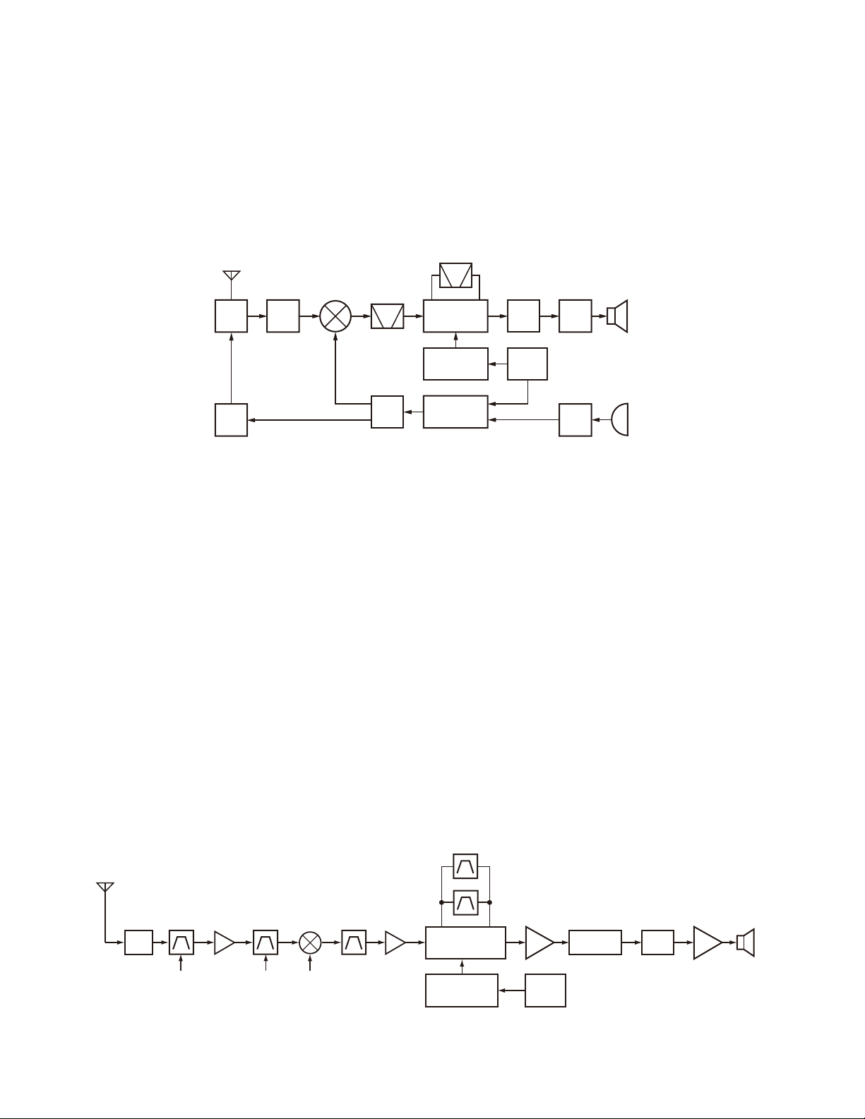
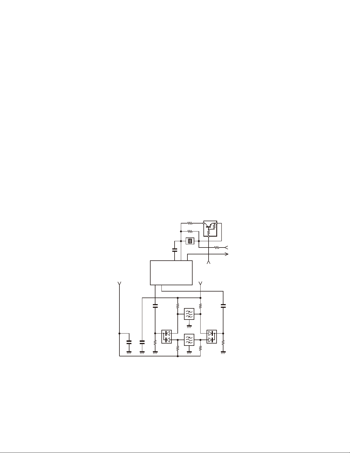
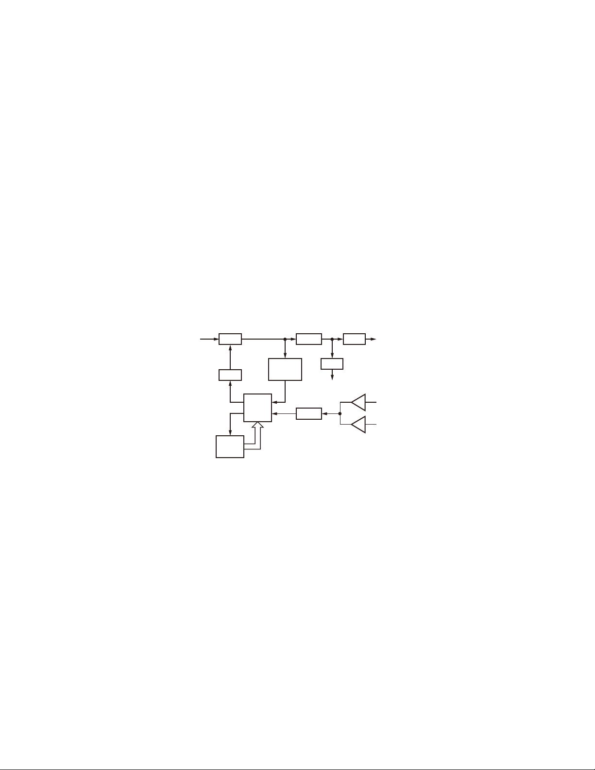
1. Frequency Confi guration
The receiver utilizes double conversion. The first IF is
49.95MHz and the second IF is 450kHz. The fi rst local oscillator signal is supplied from the PLL circuit.
The PLL circuit in the transmitter generates the neces-
sary frequencies. Figure 1 shows the frequencies.
TX/RX : 350~390MHz
ANT
ANT
SW
TX
AMP
1st MIX
RF
AMP
300.05~
340.05MHz
350~390MHz
Fig. 1 Frequency confi guration /
MCF
49.95MHz
RF
AMP
电路说明
1. 频率构成
接收部采用二次变频超外差方式。第一中频为 49.95M H z,
第二中频为 450kHz。第一本振频率信号由锁相环电路提供。
发射部由锁相环电路直接产生所需要的频率。图 1 显示各
种频率。
CF
450kHz
SP
IF
SYSTEM
50.4MHz
X3
multiply
PLL
VCO
VOL
TCXO
图 1 频率构成
AF
AMP
16.8MHz
MIC
MIC
AMP
2. Receiver System
The receiver system is shown in Figure 2.
2-1. Front End (RF AMP) Circuit
The signal coming from the antenna passes through the
transmit/receive switching diode circuit (D604, D605, D606
and D608), passes through a BPF (L717 and L718), and is
amplifi ed by the RF amplifi er (Q705).
The resulting signal passes through a BPF (L711, L712
and L713) and goes to the mixer. These BPFs are adjusted
by variable capacitors (D703, D704, D705, D706 and D707).
The input voltage to the variable capacitor is regulated by
voltage output from the DC amplifi er (IC19).
2-2. First Mixer
The signal from the front end is mixed with the fi rst local
oscillator signal generated in the PLL circuit by Q704 to produce a fi rst IF frequency of 49.95MHz.
The resulting signal passes through the XF701 MCF to
cut the adjacent spurious and provide the optimum characteristics, such as adjacent frequency selectivity.
ANT
Q705
BPF
ANT
SW
TUNE TUNE
RF
AMP
BPF
Q704
1st MIX
1st Local
XF701
MCF
Q703
IF AMP
2. 接收部系统
接收部系统的如图 2 所示。
2-1. 前级 ( 射频放大器 ) 电路
从天线接收的信号进入发送 / 接收转换开关二极管电路
(D604、D605、D606 和 D608),然后通过 BPF(L717 和 L718),
并且被射频放大器 (Q705) 放大。
此信号通过 BPF(L711、L712 和 L713) 然后进入混频。这些
BP F 被可变电容器 (D703、D704、D705、D706 和 D707) 调整。
输入可变电容器的电压被经直流放大器 ( I C19) 的电压输出调
整。
2-2. 第一混频器
前端的信号与 P LL 电路产生的第一本振信号在 Q704 混频,
生成 49.95MHz 频率的第一中频信号。
生成的信号通过 XF701 MCF。
CF702
CF701
IC701
IF, MIX, DET
Q701
X3 multiply
2nd Local
IC10
AF AMP
X501
TCXO
16.8MHz
IC13
AQUA-L
IC16
VOL
IC18
AF PA
SP
12
Fig. 2 Receiver system /
图 2 接收部系统
TK-3178(L
)
CIRCUIT DESCRIPTION /
2-3. IF Amplifi er Circuit
The fi rst IF signal is passed through a four-pole monolithic
crystal fi lter (XF701) to remove the adjacent channel signal.
The fi ltered fi rst IF signal is amplifi ed by the fi rst IF amplifi er
(Q703) and then applied to the lF system IC (IC701). The IF
system IC provides a second mixer, second local oscillator,
limiting amplifi er, quadrature detector and RSSI (Received
Signal Strength Indicator). The second mixer mixes the fi rst
IF signal with the 50.4MHz of the second local oscillator
output (TCXO X501) and produces the second IF signal of
450kHz.
The second IF signal is passed through the ceramic fi lter
(Wide: CF701, Narrow: CF702) to remove the adjacent channel signal. The fi ltered second IF signal is amplifi ed by the
limiting amplifi er and demodulated by the quadrature detector with the ceramic discriminator (CD701). The demodulated signal is routed to the audio circuit.
2-4. Wide/Narrow Switching Circuit
Wide and Narrow settings can be made for each channel
by switching the ceramic fi lters CF701 (Wide), CF702 (Narrow). The Wide and Narrow is output from IC4.
D701 and D702 are switched to ceramic fi lters when a
Wide/Narrow level is selected.
Q702 turns on/off with the Narrow and the IC701 detector output level is changed to maintain a constant output
level during wide or narrow signals.
电路说明
2-3. 中频放大电路
第一中频信号通过晶体滤波器 ( XF701) 消除相邻信道的信
号。经滤波的第一中频信号被第一中频放大器 (Q703) 放大并
进入中频系统芯片 (I C701)。中频系统芯片提供第二混频器、
第二本振信号、限幅放大器、正交检测器和 RSSI( 接收信号
强度指示器 )。第二混频器将第一中频信号与 50.4MHz 的第二
本振信号输出 (TCXO X501) 进行混频,并生成 450kHz 的第二
中频信号。
第二中频信号通过陶瓷滤波器 ( 宽 :C F701、窄 : C F702) 继
续消除相邻信道的信号。经滤波的第二中频信号被限幅放大
器放大并被带有陶瓷鉴频器 ( C D701) 的正交检测器解调。经
解调的信号进入音频电路。
2-4. 宽 / 窄切换电路
通过切换陶瓷滤波器 CF701( 宽 )、CF702( 窄 ) 可以对每一
信道进行宽,窄设置。宽、窄控制信号从 IC4 输出。
选择宽 / 窄电平时,将 D701 和 D702 切换到陶瓷滤波器。
在宽或窄信号期间,Q702 随窄信号打开 / 关闭,IC701 检
测器输出电平变为保持恒定输出电平。
R719
R717
Q702
IC701
Narrow
C702
C701
IFI
MXO
C708
D702 D701
R708
Fig. 3 Wide/Narrow switching circuit /
2-5. Audio Amplifi er Circuit
The demodulated signal from IC701 is amplifi ed by IC10,
and goes to AF amplifi er through IC13.
The signal then goes through an volume control (IC16),
and is routed to an audio power amplifi er (IC18) where it is
amplifi ed and output to the speaker.
R718
Narrow
Wide
R702
R703
C719
R705
R706
CD701
QUAD
IFOUT
CF701
CF702
AFOUT
图 3 宽 / 窄切换电路
2-5. 音频放大器电路
来自于 I C701 的解调信号被 IC10 放大,并通过 IC13 送到
AF 放大器。
信号通过 A F 音量控制 ( IC16),在音频功率放大器 ( I C18)
进行放大后输出到扬声器。
5C
AFOUT
C709
R701
13
TK-3178(L
)
CIRCUIT DESCRIPTION /
2-6. Squelch Circuit
Part of the AF signal from the IC enters the FM IC (IC701)
again, and the noise component is amplifi ed and rectifi ed by
a fi lter and an amplifi er to produce a DC voltage corresponding to the noise level.
The DC signal from the FM IC goes to the analog port of
the microprocessor (IC7). IC7 determines whether to output
sounds from the speaker by checking whether the input
voltage is higher or lower than the preset value.
To output sounds from the speaker, IC7 sends a high signal to the AM2 line and IC5 sends a high signal to the AM1
line, and turns IC18 on through Q23, Q24, Q27, Q28 and
Q35. (See Figure 4)
Fig. 4 Audio amplifi er circuit and squelch circuit /
IC701
FM IF
ANSQL
IC7
MCU
IC5
Shift register
QT/DQT
LSDI
CLK, DATA,STD, LOADN
HSDI
AM2
AM1
2-6. 静噪电路
FM IC(IC701) 输出的 AF 信号的一部分再进入 IC,噪声成
份通过滤波器和放大器进行放大和修正,生成与噪声电平相
应的 DC 电压。
DC 信号通过 FM IC 被送到微处理器的模拟端口 (IC7)。IC7
通过检测输入的电压是高于还是低于预设值来决定是否从扬
声器输出声音。
由扬声器输出声音时,IC7 发送高电平信号给 AM2 线和 IC5
发送高电平信号给 A M1 线,通过 Q23、Q24、Q27、Q28 和 Q35
打开 IC18。( 见图 4)。
IC10
IF AMP
SIGNAL
DTMF
IC11
LPF
IC15
BPF & Compalater
Q22
SW
IC16
VOL
2-tone
IC18
AF PA
SW
Q23,24,27
电路说明
IC13
AQUA-L
Q28,35
SW
图 4 音频放大器电路和静噪电路
SP
3. Transmitter System
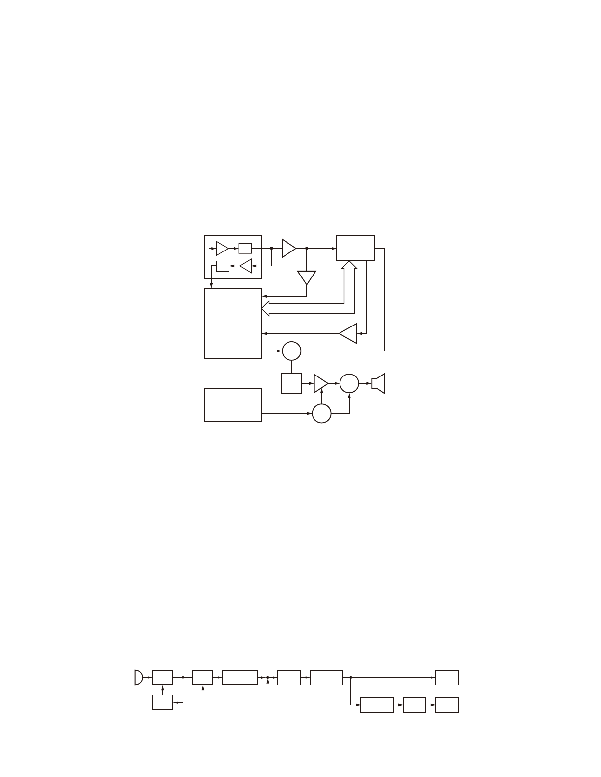
3-1. Microphone Amplifi er Circuit
The signal from microphone amplifi ed by IC13 (1/2) and
limited by AGC circuit composed of D30, D31, Q25 and
Q26, and goes through mute switch (Q30). IC13 is composed of high-pass fi lter, low-pass fi lter and pre-emphasis/
IDC circuit.
The signal enters the summing amplifier consisting of
IC12 (2/2), and passes through the D/A converter (IC16) for
the maximum deviation adjustment, and is mixed with the
low speed data from the MCU (IC7).
The output signal from the D/A converter goes to the
VCO modulation input. The other output signal from the D/
A converter passes through the D/A converter (IC16) again
for the BAL adjustment, and the buffer amplifi er (IC17), and
goes to the TCXO modulation input.
IC13
(1/2)
14
MIC Q30
AMP
AGC
D30,31
Q25,26
SW
MMUTE
Fig. 5 Microphone amplifi er circuit /
IC13
AQUA-L
LSD
OUT
3. 发射机系统
3-1. 麦克风放大器电路
麦克风的信号被 IC13(1/2) 放大,并受由 D30、D31、Q25
和 Q26 组成的 AGC 电路的限幅,然后通过静音开关 (Q30)。
IC13 由高通滤波器、低通滤波器和预加重 /IDC 电路组成。
信号送入由 I C12(2/2) 组成的加法放大器,通过最大频偏
调节的数模转换器 (IC16),然后与 MCU(IC7) 的低速数据混合。
数模转换器的输出信号送入 V CO 调制输入。数模转换器的
其他输出信号再次通过 BA L 调节的数模转换器 (IC16) 和缓冲
放大器 (IC17),然后送入 TCXO 调制输入。
IC12
(2/2)
SUM
AMP
IC16
O2
I2
D/A
IC16
O8
I8
D/A
图 5 麦克风放大器电路
VCO
IC17 X701
BUFF
AMP
TCXO
TK-3178(L
)
CIRCUIT DESCRIPTION /
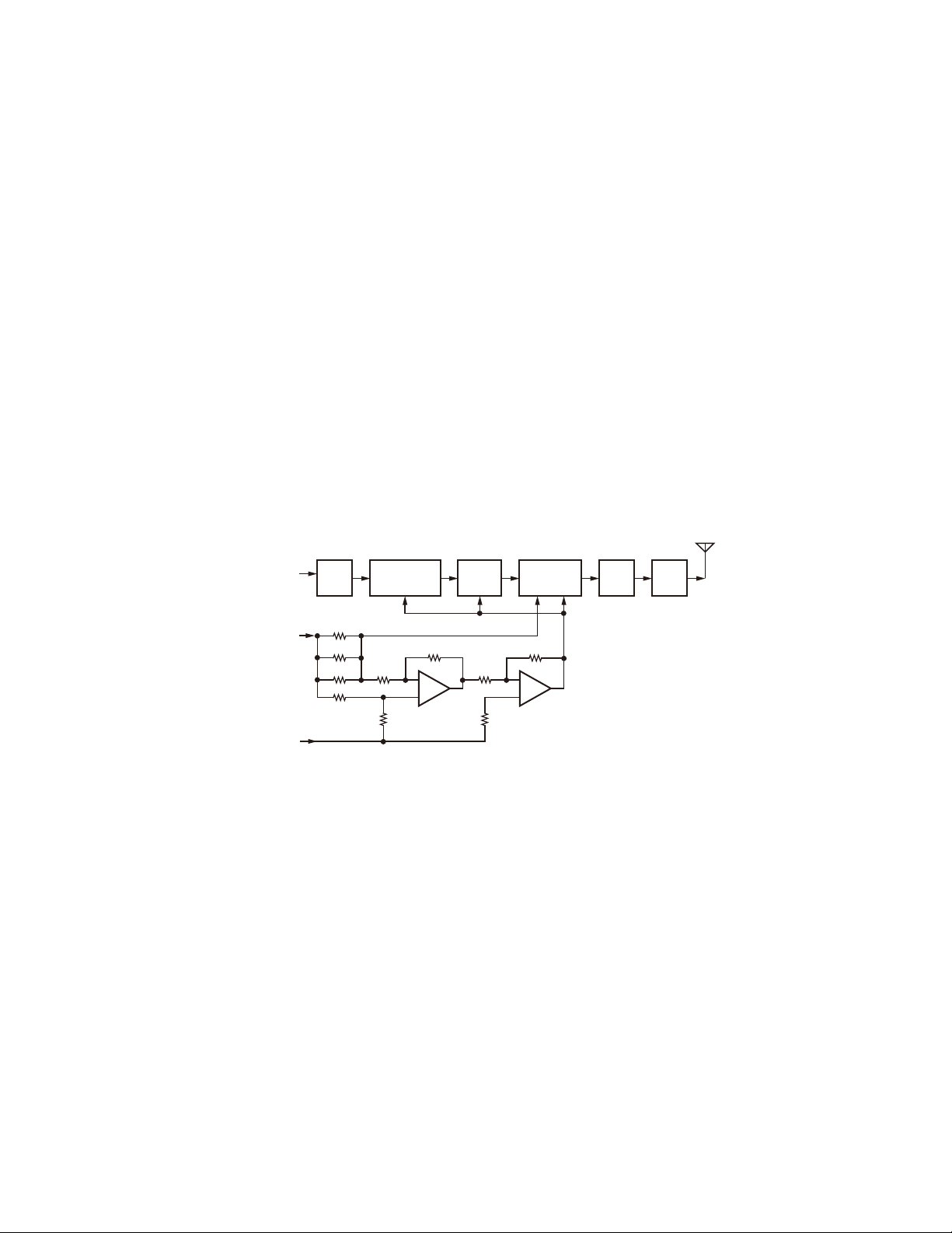
3-2. Drive and Final Amplifi er Circuit
The signal from the T/R switch (D516 is on) is amplifi ed
by the pre-drive (Q602) and drive amplifi er (Q603) to 50mW.
The output of the drive amplifi er is amplifi ed by the RF
fi nal amplifi er (Q604) to 4.0W (1W when the power is low).
The RF fi nal amplifi er consists of two MOS FET stages.
The output of the RF final amplifier is then passed
through the harmonic fi lter (LPF) and antenna switch (D604
and D605) and applied to the antenna terminal.
3-3. APC Circuit
The APC circuit always monitors the current flowing
through the RF power amplifi er (Q604) and keeps a constant
current. The voltage drop at R621, R623 and R629 is caused
by the current fl owing through the RF fi nal amplifi er and this
voltage is applied to the differential amplifi er IC601 (1/2).
IC601 (2/2) compares the output voltage of IC601 (1/2)
with the reference voltage from IC7. The output of
IC601 (2/2) controls the VG of the RF power amplifi er, drive
amplifi er and pre-drive amplifi er to make both voltages the
same.
The change of power high/low is carried out by the
change of the reference voltage.
From
T/R SW
(D516)
+B
Q601
RF
AMP
R621
R623
R629
Q602
Pre-DRIVE
AMP
电路说明
3-2. 驱动器和终端放大器电路
来自于 T/R 开关 (D516 ON) 的信号被预驱动放大器 (Q602)
和驱动放大器 (Q603) 放大到 50mW。
驱动放大器的输出被 RF 功率放大器 (Q604) 放大到 4.0W( 当
低功率时为 1W)。RF 功率放大器由 2 个 MOS FET 构成。
RF 功率放大器的输出通过谐波滤波器 (LPF) 和天线开关
(D604 和 D605) 并且送到天线终端。
3-3. 自动功率控制 (APC) 电路
AP C 电路一直监视通过射频功率放大器 (Q604) 的电流并
保持电流稳定。经过射频功率放大器的电流的变化会引起
R621、R623 和 R629 的电压降低,此电压送到差分放大器
IC601(1/2)。
I C601(2/2) 将 I C601(1/2) 的输出电压与来自 IC7 的参考
电压进行比较。IC601(2/2) 的输出电压控制射频功率放大器、
驱动放大器、预驱动放大器的 VG,使电压保持一致。
功率高 / 低的变化是通过变更参考电压来实现的。
ANT
Q603
DRIVE
AMP
Q604
RF FINAL
AMP
VDD VG
D604,605
ANT
SW
LPF
IC601
PC
(IC7)
(1/2)
Fig. 6 Drive and fi nal amplifi er circuit and APC circuit /
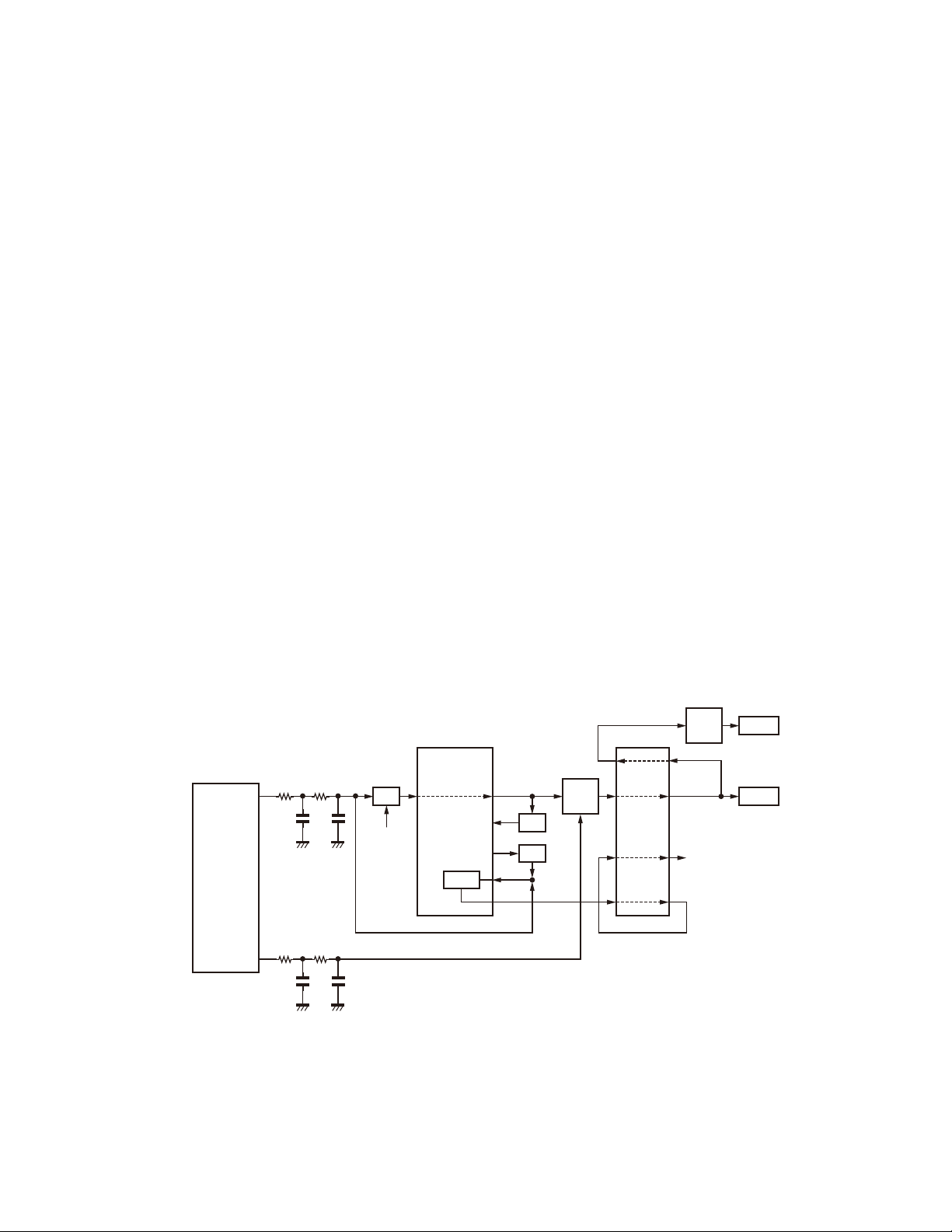
4. Frequency Synthesizer Circuit
4-1. Frequency Synthesizer
The frequency synthesizer consists of the TCXO (X501),
VCO, PLL IC (IC501) and buffer amplifi ers.
The TCXO generates 16.8MHz. The frequency stability
is 2.5ppm within the temperature range of –30 to +60°C.
The frequency tuning and modulation of the TCXO are done
to apply a voltage to pin 1 of the TCXO. The output of the
TCXO is applied to pin 8 of the PLL IC.
The VCO consists of 2VCO and covers a dual range of
the 300.05~340.05MHz and the 350~390MHz. The VCO
generates 300.05~340.05MHz for providing to the fi rst local
signal in receive. The operating frequency is generated by
Q502 in transmit mode and Q503 in receive mode. The oscillator frequency is controlled by applying the VCO control
voltage, obtained from the phase comparator (IC501) to the
variable capacitor diodes (D505 and D507 in transmit mode
and D509 and D511 in receive mode).
IC601
(2/2)
图 6 驱动器和终端放大器电路和自动功率控制 (APC) 电路
4. 频率合成器电路
4-1. 频率合成器
频率合成器由 TCXO(X501)、VCO、PLL IC(IC501) 和缓冲放
大器组成。
TCXO 产生 16.8MHz 的频率。在温度为 -30 ~ +60℃的范围内,
频率的稳定性为 2.5ppm。进行频率调谐和 TCXO 调制,以便给
TCXO 的针脚 1 提供电压。TCXO 的输出加在 PLL IC 的针脚 8 上。
VCO 由 2VCO 组成,并且覆盖了 300.05 ~ 340.05MHz 和 350
~ 390MHz 双波段。VCO 产生 300.05 ~ 340.05MHz 的频率,以
提供接收的第一个本振信号。发射模式时,操作频率由 Q502
产生,而接收模式时,操作频率由 Q503 产生。振荡频率由加
在 V CO 上的控制电压控制,控制电压从可变电容二极管 ( 在
发射模式是 D505 和 D507,在接收模式是 D509 和 D511) 的相
位比较器 (IC501) 处获得。
15
TK-3178(L
)
CIRCUIT DESCRIPTION /
The RX pin of IC4 goes “low” in receive mode causing
Q503 and Q504 (2/2) turn on. The TX pin goes “low” in
transmit mode causing Q502 and Q504 (1/2) turn on.
The outputs from Q502 and Q503 are amplifi ed by buffer
amplifi er (Q506) and doubled by Q501 and then sent to PLL
IC.
The PLL IC consists of a prescaler, reference divider,
phase comparator, charge pump (The frequency step of the
PLL circuit is 5 or 6.25kHz). The input signal from the pins 8
and 5 of the PLL IC is divided down to the 5 or 6.25kHz and
compared at phase comparator. The pulsed output signal
of the phase comparator is applied to the charge pump and
transformed into DC signal in the loop fi lter (LPF). The DC
signal is applied to the CV of the VCO and locked to keep
the VCO frequency constant.
PLL data is output from PLLDAT (pin 18), PCK (pin 17) and
PLE (pin 10) of the microprocessor (IC7). The data are input
to the PLL IC when the channel is changed or when transmission is changed to reception and vice versa. A PLL lock
condition is always monitored by the pin 7 (UL) of the microprocessor. When the PLL is unlocked, the UL goes low.
TX
RX
CV
Doubler
LPF
IC501
20
PLL
15
UL
MCU
PLLDT,PCK,PLE
IC7
电路说明
IC4 的 RX 针脚在接收模式时为“低”电位,使 Q503 和
Q504(2/2) 打 开。T X 针脚在发射模式时为“低”电位,使
Q502 和 Q504(1/2) 导通。
Q502 和 Q503 的输出由缓冲放大器 ( Q506) 放大,并由 Q501
倍频,然后发送到 PLL IC。
PLL IC 由预计数器、基准除法器、相位比较器、电荷泵组
成 (PLL 电路的频率步长为 5kHz 或 6.25kHz)。PLL IC 的针脚
8 和 5 的输入信号下分成 5k H z 或 6.25k H z,并在相位比较器
处进行比较。相位比较器的脉冲输出信号加在电荷泵上,并
转换成环路滤波器 (LPF) 的 DC 信号。DC 信号加在 VCO 的 CV
上并锁定,使 VCO 的频率恒定。
PL L 数据从微处理器 ( IC7) 的 PLLDAT( 针脚 18),PCK( 针
脚 17) 和 PLE( 针脚 10) 输出。当信道改变时,或当由发射变
为接收或由接收变为发射时,数据输入 PL L I C。P LL 的锁定
条件总是由微处理器的针脚 7(UL) 监控。当PLL 失锁时,UL
为低电位。
Q507
BUFFVCO
Q501
x2
5
TCXO
8
X501
SW D515
To mixer
VC
D516
SW
IC17
To
drive
amp
FC
BAL
Fig. 7 PLL block diagram /
5. Control Circuit
The control circuit consists of microprocessor (IC7) and
its peripheral circuits. It controls the TX-RX unit. IC7 mainly
performs the following;
1) Switching between transmission and reception by PTT
signal input.
2) Reading system, zone, frequency, and program data from
the memory circuit.
3) Sending frequency program data to the PLL.
4) Controlling squelch on/off by the DC voltage from the
squelch circuit.
5) Controlling the audio mute circuit by decode data input.
6) Transmitting tone and encode data.
16
图 7 PLL 方块图
5. 控制电路
控制电路是由微处理器 (IC7) 和外部电路构成。它控制
TX-RX 单元。IC7 的主要功能如下 :
1) 根据 PTT 的输入信号来转换发射和接收状态。
2) 从存储电路读出系统、区域、频率以及编程数据。
3) 发送频率数据给 PLL。
4) 根据静噪电路输出的 DC 电压来控制静噪的开启和关闭。
5) 根据解码数据控制音频静音。
6) 发射 Tone 及编码数据。
TK-3178(L
)
CIRCUIT DESCRIPTION /
5-1. Frequency Shift Circuit
The microprocessor (IC7) operates at a clock of 11.0592
MHz. This oscillator has a circuit that shifts the frequency by
Beat shift switch (Q17,Q18).
A beat sound may be able to be evaded from generation
if “Beat Shift” is set to ON when it is generated in the internal spurious transmission modulated sound of a transceiver.
XIN
X1
XOUT
C63
IC7
MCU
SHIFT
Fig. 8 Frequency shift circuit /
5-2. Memory Circuit
Memory circuit consists of the MCU (IC7) and a flash
memory (IC8). A fl ash memory has a capacity of 16M bits
and contains the transceiver control program for the MCU. It
also stores the data for transceiver channels and operating
parameter that are written by the FPU. This program can be
easily written from an external devices.
The EEPROM (IC9) stores the last channel data, the scan
on status, and other parameters.
电路说明
5-1. 频率偏移电路
微处理器 (IC7) 在 11.0592MHz 时钟下工作。此振荡器有可
以被拍频偏移开关 (Q17,Q18) 变换频率的电路。
如果“拍频偏移”被设定为 ON,可以避免产生拍频声音。
C64
C60
5-2. 存储电路
存储电路由 MCU(IC7) 和闪存 (IC8)组成。闪存的容量为
16M 位,并包括 MCU 的手持对讲机控制程序。它也保存手持对
讲机信道的数据和由 F PU 写入的操作参数。此程序很容易从
外部设备写入。
EEPROM(IC9) 保存最后的信道数据、扫描状态和其他参数。
C62
Q17Q18
“H” : OFF
“L” : ON
图 8 频率偏移电路
Flash memory
■
Note: The fl ash memory stores the data that is written by
the FPU (KPG-127D), and firmware program (User mode,
Test mode, Tuning mode, etc.). This data must be rewritten
when replacing the fl ash memory.
EEPROM
■
Note: The EEPROM stores tuning data (Deviation, Squelch,
etc.).
Realign the transceiver after replacing the EEPROM.
IC8
Fig. 9 Memory circuit /
5-3. Low Battery Warning
The battery voltage is monitored by the microprocessor
(IC7 pin 138: BATTLVL). When the battery voltage falls below the voltage set by the Low Battery Warning adjustment
during the transmission, the red LED blinks to notify the
operator that it is time to replace the battery (When the “On
TX” option (default setting) under the Battery Warning / status function in the FPU is selected.). If the battery voltage
falls below 5.9V, the transceiver does not transmit and the
warning tone beeps while the PTT switch is pressed.
■闪存
注意 :
闪存保存由 FPU(KPG-127D) 写入的数据和固件程序 ( 用
户模式、测试模式、调谐模式等 )。更换闪存后,此数据必须
重写。
■ EEPROM
注意 :
EEPROM 保存调谐数据 ( 频偏、静噪等 )。
更换 EEPROM 后,请重新校正手持对讲机。
IC7
MCU
IC9
EEPROMFLASH
图 9 存储电路
5-3. 低电池电量警告
电池电压由微处理器 (I C7 针脚 138:BATTLVL) 监控。发射
期间,当电池电压低于低电池电量警告调节设置的电压时,
红色 L ED 闪烁,通知操作者应该更换电池了 ( 当选择了 F PU
电池告警 / 状态功能下的“On TX( 发射时 )”选项(默认)时)。
如果电池电压低于 5.9V,按下 P T T 开关时手持对讲机不发射
并响起警告音。
17
TK-3178(L
)
CIRCUIT DESCRIPTION /
Low battery warning Battery status
The red LED blinks during the
transmission.
The red LED blinks and the
warning tone beeps while the
PTT switch is pressed.
5-4. Battery Type Detection
The transceiver automatically detects the battery type,
measuring the resistance between the S-terminal and +
terminal on the battery pack and changes the supplied voltage to the S-terminal as below. The microprocessor then
detects the battery type.
Resistor value Battery type Input voltage of S-terminal
1.8M
Ω
560k
Ω
220k
Ω
OPEN Battery case 0~0.3V
Li-ion 0.3~1.3V
Ni-Cd 1.3~2.6V
Ni-MH 2.6~5.0V
The battery voltage is low but
the transceiver is still usable.
The battery voltage is low and
the transceiver is not usable to
make calls.
R27
SB
R28
Fig. 10 Low battery warning /
电路说明
低 电 池 电 量 警 告 电 池 状 态
发射期间红色 LED 闪烁。
按下 PTT 开关时,红色 LED 闪
烁并响起警告音。
138
BATTLVL
IC7
MCU
图 10 低电池电量警告
5-4. 电池类型检测
手持对讲机自动地检测电池类型,测量电池组在 S 终端和
+终端之间的电压的变化。然后微处理器检测电池类型。
阻 抗 电池类型 S 终端的输入电压
1.8MW Li-ion 0.3~1.3V
560kW Ni-Cd 1.3~2.6V
220kW Ni-MH 2.6~5.0V
开放 电池盒 0~0.3V
电池电压低,但手持对讲机仍
能使用。
电池电压低,不能使用手持对
讲机进行呼叫。
5-5. Key Input
Keys and channel selector circuit.
The signal from the keys and channel selector are directly
input to the microprocessor, as shown in Figure 11.
KEY1O
KEY2O
KEY3O
107
108
109
2
13
4
56
89
7
0#
*
IC7
MCU
KEY4O
114
103
S
A
B
C
5-5. 键输入
键和信道选择电路。
如图 11 所示,键和信道选择器的信号被直接输入微处理器。
Selector
89
102
EN2
EN3
KEY1I
KEY2I
104
KEY3I
105
KEY4I
106
SIDE2
127
SW2
SIDE1
126
SW1
AUX
128
AUX
SW
PTT
125
PTT
SW
18
Fig. 11 Key input /
图 11 键输入
TK-3178(L
)
CIRCUIT DESCRIPTION /
5-6. LCD
The LCD is controlled using the bus lines on the connector (CN82) of the TX-RX unit (B/4). It corrects the LCD contrast voltage using VR1.
6. Signaling Circuit
6-1. Encode
Low-speed data (QT, DQT)
■
Low-speed data is output from pin 33 of the MCU. The
signal passes through MOD amplifi er (IC12 1/2), and goes to
the buffer amplifi er (IC17 2/2). The signal is mixed with the
audio signal and goes to the VCO and TCXO (X501) modulation input after passing through the D/A converter (IC16) for
BAL adjustment.
High-speed data (DTMF)
■
High-speed data (HSD) is output from pin 4 of the MCU.
The signal passes through a low-pass CR fi lter and provides
a TX HSD tone and a RX HSD tone. TX HSD deviation making an adjustment by microprocessor is passed through the
switch (IC14) and then applied to the audio processor (IC13).
The signal is mixed with the audio signal and goes to the
VCO and TCXO. The RX HSD tone is passed a summing
amplifi er (IC18). The D/A converter (IC16) for audio control,
audio power amplifi er and then to the speaker.
电路说明
5-6. LCD
LCD 是用 TX-RX 单元 (B/4) 的连接口 (CN82) 的总线来控制
的。使用 VR1 补正 LCD 的对比度电压。
6. 信令电路
6-1. 编码
■低速数据 (QT, DQT)
低速数据从 MCU 的针脚 33 输出。信号通过 MOD 放大器 (IC12
1/2),然后送入缓冲放大器 (IC17 2/2)。此信号与音频信
号混合,通过 BAL 调节的数模转换器 ( I C16) 后送入 V C O 和
TCXO(X501) 调制输入。
■高速数据 (DTMF)
高速数据 (HSD) 从 MCU 的针脚 4 输出。信号通过低通 CR 滤
波器,并提供 TX HSD 音和 RX HSD 音。微处理器调节 TX HSD
的频偏并通过开关 (IC14),然后加到音频处理器 (IC13) 上。
此信号与音频信号混合,然后送入 V C O 和 TCXO。RX HSD
音通过加法放大器 (I C18)。经过用于音频控制的数模转换器
(IC16)、音频功率放大器,然后到扬声器。
MSK
■
MSK signal is output from pin 6 of IC13. The signal passes through the D/A converter (IC16) and is routed to the
VCO. When encoding MSK, the microphone input signal is
muted.
IC13
AQUA-L
HSDO
IC7
MCU
LSDOUT
33
4
IC14
RX Audio
SW
EXTLIMIN
5
SUM
Fig. 12 Encode /
■ MSK
MS K 信号从 IC13 的针脚 6 输出。此信号通过数模转换器
(IC16),然后发送给 VCO。编码 MSK 时,麦克风输入信号被静音。
IC17 (1/2)
MOD
6
RXAF
SW
SW
IC12
MOD
AMP
O8
I2
I3
I4
IC16
O2
O3
O4
BUFF
AMP
I8
AF AMP
TCXO
VCO
图 12 编码
19

TK-3178(L
)
CIRCUIT DESCRIPTION /
6-2. Decode
QT/DQT
■
The output signal from IF IC (IC701) enters the microprocessor (IC7) through IC11. IC7 determines whether the QT
or DQT matches the preset value, and controls the AM1
using IC5 and the speaker output sounds according to the
squelch results.
DTMF, MSK
■
The DTMF and MSK input signal from the IF IC (IC701) is
amplifi ed by IC10 and goes to IC13. The decoded information is then processed by the MCU.
7. Power Supply
There are fi ve 5V and two 3.3V power supplies for the microprocessor: 5M, 5MS, 5C, 5R, 5T, 33M and 33MS.
5M and 33M is always output while the power is on. 5M
is always output, but turns off when the power is turned off
to prevent malfunction of the microprocessor.
5C is a common 5V and is output when SAVE is not set
to OFF.
5R is 5V for reception and output during reception.
5T is 5V for transmission and output during transmission.
电路说明
6-2. 解码
■ QT/DQT
IF IC(IC701) 的输出信号通过 I C11 送入
IC7 确认 QT 或 DQT 是否与预设值匹配,并用 IC5 控制 AM1,
然后扬声器根据静噪结果输出声音。
■ DTMF, MSK
IF IC(IC701) 的 DTMF 和 MSK 输入信号由 IC10 放大,然后
送入 IC13。然后由 MCU 处理解码信息。
7. 电源
微处理器
5R、5T、33M 和 33MS。
电源打开时,5M 和 33M 总是输出。5M 总是输出,但电源关
闭时 5M 关闭,以防止
5C 是普通的 5V 电源,它在 SAVE 没有设为 OFF 时输出。
5R 是接收用 5V 电源,它在接收期间输出。
5T 是发射用 5V 电源,它在发射期间输出。
有5个5V电源和2个3.3V 电 源。5M、5M S、5C、
微处理器
出现故障。
微处理器
(IC7)。
20
TK-3178(L
)
SENCONDUCTOR DATA /
MCU: 30875MHB069GP (TX-RX unit IC7)
Pin No. Port Name I/O Function
1 SFTOE O BU4094 output enable
2 SFTSTB O BU4094 strobe
3 PC O TX APC/ VC tune
4 HSDO O High speed data output
5 LCONT O LCD contrast adjust
6 MDSW I Man down SW input
7 UL I PLL unlock detect
8 SHIFT O Beat shift
9 OPTDET I Option detection
10 PLE O PLL enable
11 5RC O 5R contorl
12 APCSW O APC SW
13 DSW O APC voltage discharge SW
14 NC - NC
15 BYTE I 8bit data bus (5V)
16 CNVSS I CNVss (GND)
17 PCK O PLL clock
18 PLLDAT O PLL data output
19 RESET I Reset
20 XOUT O 11.0592MHz
21 DGND I DGND (GND)
22 XIN I 11.0592MHz
23 VCC1 - VCC1 (5V)
24 NMI I NMI
25 INT I Low battery voltage INT
26 BB RDF/FD I AQUA RDF/FD
27 TCLK/DTRDO I AQUA TCLK and DTR DO
28 HSDIN I High speed data input
29 AFDAT O AQUA TDATA and DTR CLK
30 AFDIO I/O AQUA DI/O
31 BEEP O Beep output
32 AFDIR O AQUA DIR
33 LSDOUT O Low speed data output
34 DTRLOAD O AQUA DTMF enable
35 SCLK O AQUA SCLK
36 AFSTD I AQUA STD
37 DACLD O DAC LD
38 TXD O Com port 0
39 VCC1 - VCC1 (5V)
40 RXD I Com port 0
41 DGND I DGND (GND)
42 NC - SCLK
43 NC - BUSY
44 TXD2 O Option board
半导体数据
微处理器 : 30875MHB069GP(TX-RX 单元 IC7)
管脚号 端口名称
1 SFTOE 输出 BU4094BCFV 输出启动
2 SFTSTB 输出 BU4094 选通脉冲
3 PC 输出 TX APC/ VC 调谐
4 HSDO 输出 高速数据输出
5 LCONT 输出 LCD 对比度调整
6 MDSW 输入 人员事故开关输入
7 UL 输入 PLL 失锁检测
8 SHIFT 输出 拍频偏移
9 OPTDET 输入 可选检测
10 PLE 输出 PLL 启动
11 5RC 输出 5R 控制
12 APCSW 输出 APC 开关
13 DSW 输出 APC 电压放电开关
14 NC - NC
15 BYTE 输入 8bit 数据总线 (5V)
16 CNVSS 输入 CNVss(GND)
17 PCK 输出 PLL 时钟
18 PLLDAT 输出 PLL 数据输出
19 RESET 输入 复位
20 XOUT 输出 11.0592MHz
21 DGND 输入 DGND(GND)
22 XIN 输入 11.0592MHz
23 VCC1 - VCC1(5V)
24 NMI 输入 NMI
25 INT 输入 低电池电压 INT
26 BB RDF/FD 输入 AQUA RDF/FD
27 TCLK/DTRDO 输入 AQUA TCLK 和 DTR DO
28 HSDIN 输入 高速数据输入
29 AFDAT 输出 AQUA TDATA 和 DTR CLK
30 AFDIO
31 BEEP 输出 提示音输出
32 AFDIR 输出 AQUA DIR
33 LSDOUT 输出 低速数据输出
34 DTRLOAD 输出 AQUA DTMF 启动
35 SCLK 输出 AQUA SCLK
36 AFSTD 输入 AQUA STD
37 DACLD 输出 DAC LD
38 TXD 输出 Com 端口 0
39 VCC1 - VCC1(5V)
40 RXD 输入 Com 端口 0
41 DGND 输入 DGND(GND)
42 NC - SCLK
43 NC - BUSY
44 TXD2 输出 选件板
输入/输出
输入/输出
功 能
AQUA DI/O
21
TK-3178(L
)
SEMICONDUCTOR DATA /
Pin No. Port Name I/O Function
45 RXD2/AIMH I Option board
46 DACCLK O DAC clock
47 DACDAT O DAC data
48 AM2 O Audio mute 2
49 5TC O 5T control
50 LEDR O Red LED
51 LEDG O Green LED
52 RDY - RDY (3.3V)
53 NC O NC
54 HOLD I HOLD
55 NC O NC
56 33MSC O 33MS control
57 VSS I VSS (GND)
58 NC - NC
59 VCC2 - VCC2 (3.3V)
60,61 NC - NC
62 NC O NC
63 RD O Flash memory read
64 NC O NC
65 WR O Flash memory write
66~68 NC - NC
69 CS0 O Flash memory chip select
70 NC O NC
71 CS2 O LCD driver chip select
72~73 A20~A19 O Address bus 20~19
74 VCC2 - VCC2 (3.3V)
75 A18 O Address bus 18
76 VSS I VSS (GND)
77~85 A17~A9 O Address bus 17~9
86 FREADY I Flash-ROM ready status
87 NC - NC
88 EN4 I Encoder 4 input
89 EN3 I Encoder 3 input
90 EN1 I Encoder 1 input
91 VCC2 - VCC2 (3.3V)
92 A8 O Address bus 8
93 DGND I DGND (GND)
94~101 A7~A0 O Address bus 7~0
102 EN2 I Encoder 2
103~106 KEY1~KEY4 I Key matrix 1~4 input
107~109 KEY1O~KEY3O O Key matrix 1~3 output
110~113 D7~D4 I/O Data bus 7~4
114 KEY4O O Key matrix 4 output
115 LCDRST O LCD reset
116~118 NC - NC
半导体数据
管脚号 端口名称
45 RXD2/AIMH 输入 选件板
46 DACCLK 输出 DAC 时钟
47 DACDAT 输出 DAC 数据
48 AM2 输出 音频静音 2
49 5TC 输出 5T 控制
50 LEDR 输出 红色 LED
51 LEDG 输出 绿色 LED
52 RDY - RDY(3.3V)
53 NC 输出 NC
54 HOLD 输入 HOLD
55 NC 输出 NC
56 33MSC 输出 33MS 控制
57 VSS 输入 VSS(GND)
58 NC - NC
59 VCC2 - VCC2(3.3V)
60,61 NC - NC
62 NC 输出 NC
63 RD 输出 闪存读出
64 NC 输出 NC
65 WR 输出 闪存写入
66~68 NC - NC
69 CS0 输出 闪存芯片选择
70 NC 输出 NC
71 CS2 输出 LCD 驱动器芯片选择
72~73 A20~A19 输出 地址总线 20~19
74 VCC2 - VCC2(3.3V)
75 A18 输出 地址总线 18
76 VSS 输入 VSS(GND)
77~85 A17~A9 输出 地址总线 17~9
86 FREADY 输入 闪存就绪状态
87 NC - NC
88 EN4 输入 选择器 4 输入
89 EN3 输入 选择器 3 输入
90 EN1 输入 选择器 1 输入
91 VCC2 - VCC2(3.3V)
92 A8 输出 地址总线 8
93 DGND 输入 DGND(GND)
94~101 A7~A0 输出 地址总线 7~0
102 EN2 输入 选择器 2
103~106 KEY1~KEY4 输入 键矩阵 1~4输入
107~109 KEY1O~KEY3O 输出 键矩阵 1~3输出
110~113 D7~D4
114 KEY4O 输出 键矩阵 4 输出
115 LCDRST 输出 LCD 复位
116~118 NC - NC
输入/输出
输入/输出
功 能
数据总线 7~4
22
TK-3178(L
)
SENCONDUCTOR DATA /
Pin No. Port Name I/O Function
119~122 D3~D0 I/O Data bus 3~0
123 AUX1 O Option board
124 EEPDAT I/O EEPROM data
125 PTT I PTT SW
126 SIDE1 I Side key 1
127 SIDE2 I Side key 2
128 AUXK I AUX key input
129 EEPCL O EEPROM clock
130 VSS I VSS (GND)
131 BATTSEL I Battery select detect
132 VCC1 - VCC1 (5V)
133 THP I TX thermal input
134 VOL IN I Volume level input
135 VOX I VOX level input
136 ASQ I RX analog squelch input
137 RSSI I RSSI level input
138 BATTLVL I Battery voltage input
139 LSDIN I Low speed data input
140 AGND I AVSS (GND)
141 CLK O Serial clock
142 VREF - VREF (5V)
143 AVCC - AVCC (5V)
144 DT I/O Serial data
半导体数据
管脚号 端口名称
119~122 D3~D0
123 AUX1 输出 选件板
124 EEPDAT
125 PTT 输入 PTT 开关
126 SIDE1 输入 Side1 键
127 SIDE2 输入 Side2 键
128 AUXK 输入 AUX 键输入
129 EEPCL 输出 EEPROM 时钟
130 VSS 输入 VSS(GND)
131 BATTSEL 输入 电池选择检测
132 VCC1 - VCC1(5V)
133 THP 输入 TX 热感输入
134 VOL IN 输入 音量电平输入
135 VOX 输入 VOX 电平输入
136 ASQ 输入 RX 模拟静噪输入
137 RSSI 输入 RSSI 电平输入
138 BATTLVL 输入 电池电压输入
139 LSDIN 输入 低速数据输入
140 AGND 输入 AVSS(GND)
141 CLK 输出 串行时钟
142 VREF - VREF(5V)
143 AVCC - AVCC(5V)
144 DT
输入/输出
输入/输出
输入/输出
输入/输出
功 能
数据总线 3~0
EEPROM 数据
串行数据
23
TK-3178(L
)
COMPONENTS DESCRIPTION /
TX-RX unit (X57-7013-06)
Ref. No. Part Name Description
IC1 IC Voltage detector / INT
IC2 IC Voltage regulator / 5V
IC3 IC Voltage detector / RESET
IC4,5 IC Shift register
IC7 IC MCU
IC8 IC Flash memory
IC9 IC EEPROM
IC10 IC DET amplifi er / VREF
IC11 IC LSD fi lter
IC12 IC TX SUM amplifi er
IC13 IC Audio processor
IC14 IC AF switch
IC15 IC RX HSD fi lter
IC16 IC D/A converter
IC17 IC TCXO buffer amplifi er
IC18 IC AF amplifi er
IC19 IC RX BPF tune voltage amplifi er
IC24 IC Volatge doubling inverter
IC25 IC Bus switch
IC26 IC Voltage regulator / 3.3V
IC27 IC LCD contrast
IC28 IC Bus switch
IC501 IC PLL system
IC601 IC Comparator (APC)
IC701 IC FM IF system
Q1 Transistor 5T voltage control
Q4 (1/2) Transistor AVR / 5C
Q4 (2/2) Transistor AVR / 5T
Q5 (1/2) FET 5TC switch
Q5 (2/2) FET SAVE switch
Q6 Transistor 5C voltage control
Q7 FET TX/RX indicator control
Q8 Transistor 5R control switch
Q9 FET 5MS control switch
Q12 Transistor Back light control
Q13 Transistor Back light DC supply
Q14 FET RX AF mute
Q15 FET SSB DC supply control switch
Q16 Transistor SSB DC supply switch
Q17,18 Transistor MCU clock shift switch
Q19 FET VOX level detector control switch
Q21 Transistor AF switch
Q22 FET AF mute switch
Q23 Transistor
AF amplifi er DC supply control
switch
元件说明
TX-RX 单元 (X57-7013-06)
有关号码 零件名称 说 明
IC1 IC 电压检测器 /INT
IC2 IC 电压调节器 /5V
IC3 IC 电压检测器 / 复位
IC4,5 IC 位移寄存器
IC7 IC 微处理器
IC8 IC 闪存
IC9 IC EEPROM
IC10 IC DET 放大器 /VREF
IC11 IC LSD 滤波器
IC12 IC TX SUM 放大器
IC13 IC 音频处理器
IC14 IC AF 开关
IC15 IC RX HSD 滤波器
IC16 IC 数 / 模转换器
IC17 IC TCXO 缓冲放大器
IC18 IC AF 放大器
IC19 IC RX BPF 调谐电压放大器
IC24 IC 倍压变换器
IC25 IC 总线开关
IC26 IC 电压调节器 /3.3V
IC27 IC LCD 对比度
IC28 IC 总线开关
IC501 IC PLL 系统
IC601 IC 比较器 (APC)
IC701 IC FM IF 系统
Q1 晶体管 5T 电压控制
Q4(1/2) 晶体管 AVR/5C
Q4(2/2) 晶体管 AVR/5T
Q5(1/2) 场效应管 5TC 开关
Q5(2/2) 场效应管 节电开关
Q6 晶体管 5C 电压控制
Q7 场效应管 TX/RX 指示灯控制
Q8 晶体管 5R 控制开关
Q9 场效应管 5MS 控制开关
Q12 晶体管 背光控制
Q13 晶体管 背光直流电源
Q14 场效应管 RX AF 静音
Q15 场效应管 SSB 直流电源控制开关
Q16 晶体管 SSB 直流电源开关
Q17,18 晶体管 MCU 时钟位移开关
Q19 场效应管 VOX 电平检测器控制开关
Q21 晶体管 AF 开关
Q22 场效应管 AF 静音开关
Q23 晶体管 AF 放大器直流电源控制开关
24
 Loading...