


UHF FM TRANSCEIVER
TK-3170
SERVICE MANUAL
E,X2 versions
Knob (Selector)
(K29-9340-13)
Knob (Volume)
(K29-9278-13)
Badge
(B43-1178-04)
Knob (PTT)
(K29-9339-03)
Key top (Side)
(K29-9341-03)
Plastic cabinet assy
(A02-3891-13)
Packing
(G53-1652-11)
© 2005-8 PRINTED IN JAPAN
B51-8738-00 (N) 355
Does not come with antenna.
Antenna is available as an option.
CONTENTS
GENERAL ................................................... 2
SYSTEM SET-UP ....................................... 2
REALIGNMENT .......................................... 3
DISASSEMBLY FOR REPAIR .................. 16
CIRCUIT DESCRIPTION ........................... 19
SEMICONDUCTOR DATA ....................... 24
COMPONENTS DESCRIPTION ............... 25
PARTS LIST .............................................. 27
EXPLODED VIEW..................................... 36
PACKING .................................................. 37
ADJUSTMENT ......................................... 38
TERMINAL FUNCTION ............................ 47
PC BOARD
TX-RX UNIT (X57-701X-XX) (A/4) ..........
TX-RX UNIT (X57-701X-XX) (B,C,D/4) ...
48
50
SCHEMATIC DIAGRAM........................... 54
BLOCK DIAGRAM .................................... 62
LEVEL DIAGRAM ..................................... 64
KSC-30 (CHARGER) ................................. 65
SPECIFICATIONS .................. BACK COVER
This product uses Lead Free solder.
TK-3170
GENERAL / SYSTEM SET-UP
INTRODUCTION
SCOPE OF THIS MANUAL
This manual is intended for use by experienced technicians familiar with similar types of commercial grade communications equipment. It contains all required service information for the equipment and is current as of the publication
date. Changes which may occur after publication are covered
by either Service Bulletins or Manual Revisions. These are
issued as required.
ORDERING REPLACEMENT PARTS
When ordering replacement parts or equipment information, the full part identification number should be included.
This applies to all parts : components, kits, or chassis. If the
part number is not known, include the chassis or kit number
of which it is a part, and a sufficient description of the required component for proper identification.
SYSTEM SET-UP
PERSONAL SAFETY
The following precautions are recommended for person-
nel safety:
• DO NOT transmit until all RF connectors are verified secure and any open connectors are properly terminated.
•SHUT OFF and DO NOT operate this equipment near electrical blasting caps or in an explosive atmosphere.
• This equipment should be serviced by a qualified technician only.
SERVICE
This radio is designed for easy servicing. Refer to the
schematic diagrams, printed circuit board views, and alignment procedures contained within.
Merchandise received
Choose the type of transceiver
Transceiver programming
Are you using the optional antenna?
NO
Are you using the speaker microphone?
NO
Delivery
Frequency range (MHz) RF power Type
TX/RX 440~470
TX/RX 470~512
A personal computer (IBM PC or compatible), programming
interface (KPG-22), and programming software (KPG-101D)
are required for programming.
(The frequency, TX power HI/LOW, and signaling data are
programmed for the transceiver.)
YES
YES
KRA-23 or KRA-27
Optional antenna
(Option)
KMC-17 or KMC-21
Speaker microphone
(Option)
4W
4W
TK-3170 E
TK-3170 X2
2
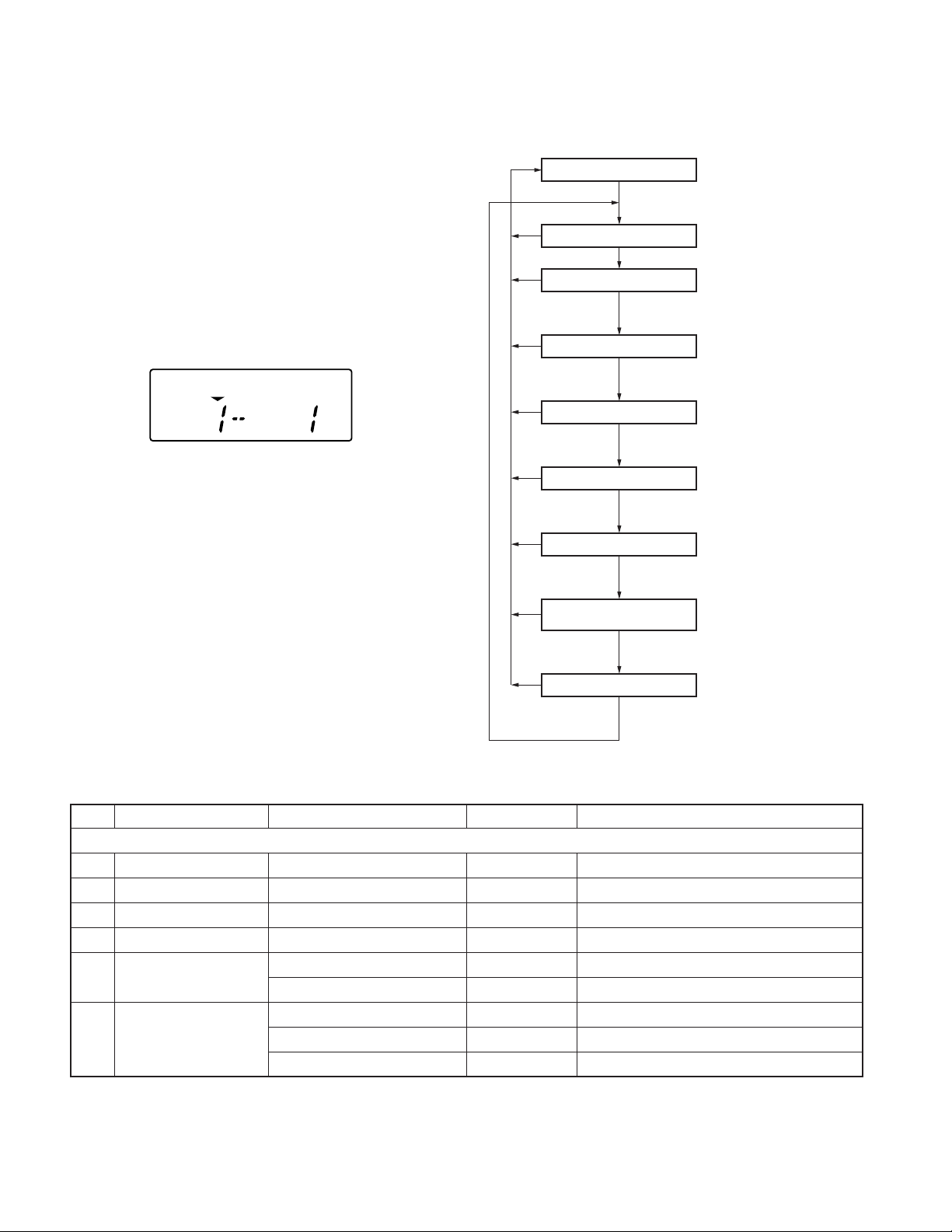
REALIGNMENT
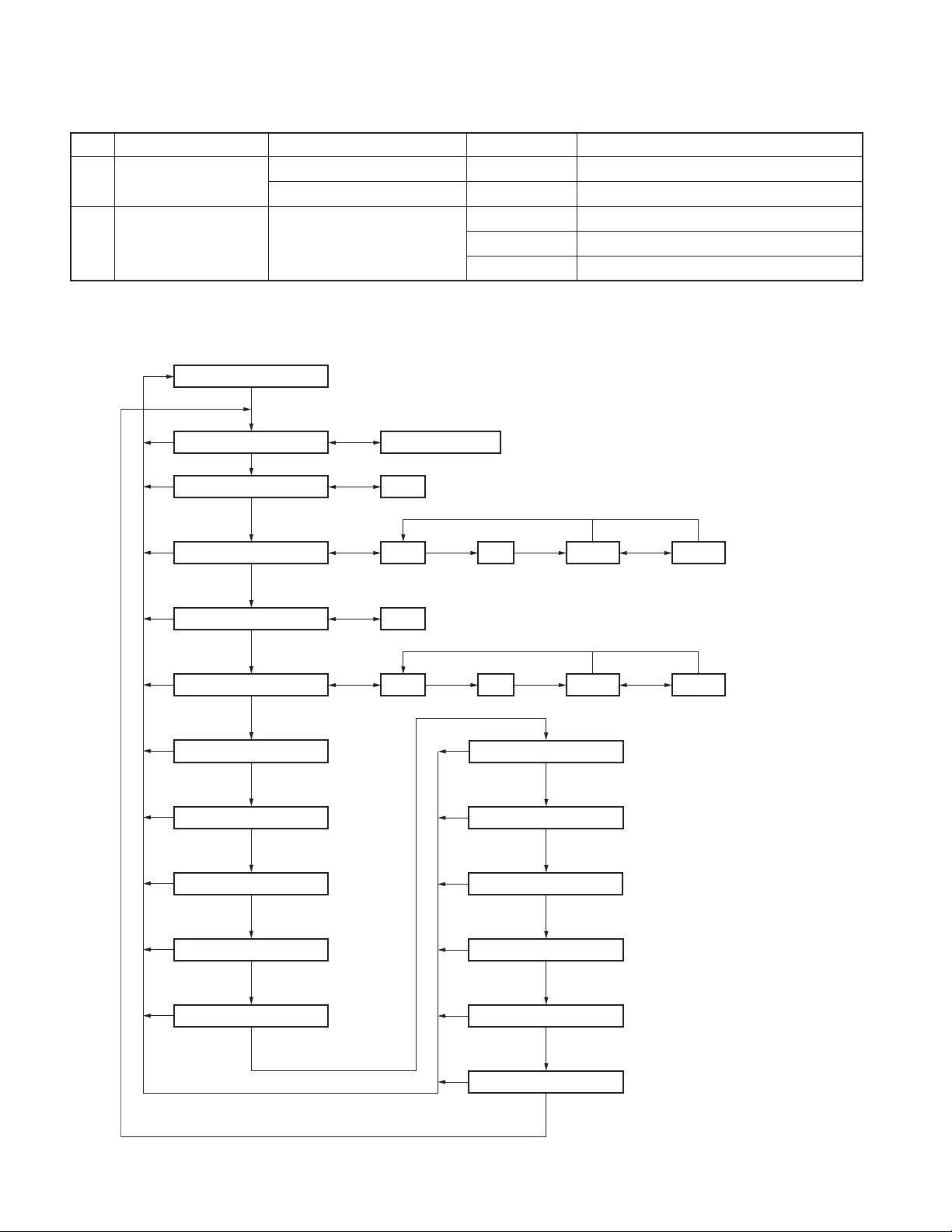
1. Modes 2. How to Enter Each Mode
User mode
Panel test mode
PC mode
Firmware
programming mode
Clone mode
Panel tuning mode
Data programming mode
PC test mode
PC tuning mode
User mode Power ON
Panel test mode [A] + Power ON
PC mode Received commands from PC
Panel tuning mode [Panel test mode] + [S]
Firmware programming mode [Side2] + Power ON
Clone mode [B] + Power ON
Firmware version information [Side1] + Power ON
Self-programming mode [C] + Power ON
Mode Operation
TK-3170
Firmware version information
Self-programming mode
Mode Function
User mode For normal use.
Panel test mode Used by the dealer to check the funda-
mental characteristics.
Panel tuning mode
PC mode Used for communication between the
Data programming
mode
PC test mode
Firmware Used when changing the main program
programming mode of the flash memory.
Clone mode Used to transfer programming data from
Firmware version Used to confirm the internal firmware
information version.
Self-programming
mode
Used by the dealer to tune the transceiver.
transceiver and PC (IBM compatible).
Used to read and write frequency data and
other features to and from the transceiver.
Used to check the transceiver using the PC.
This feature is included in the FPU.
See panel tuning.
one transceiver to another.
You can program the frequency signaling and
other function using only the transceiver.
3. Panel Test Mode
Setting method refer to ADJUSTMENT.
4. Panel Tuning Mode
Setting method refer to ADJUSTMENT.
5. PC Mode
5-1. Preface
The transceiver is programmed by using a personal computer, programming interface (KPG-22) and programming
software (KPG-101D).
The programming software can be used with an IBM PC
or compatible. Figure 1 shows the setup of an IBM PC for
programming.
IBM-PC
KPG-22
KPG-101D
RF Power meter
or SSG
Tuning cable
(E30-3216-05)
Fig. 1
Gray
Gray/Black
1.5D-XV Lead wire
1.5D-XV Shield wire
+
SP
–
+
MIC
–
3

TK-3170
REALIGNMENT
5-2. Connection Procedure
1. Connect the transceiver to the personal computer with
the interface cable.
2. When the POWER switch on, user mode can be entered
immediately. When PC sends command the transceiver
enter PC mode, and “PROGRAM” is displayed on the
LCD.
When data transmitting from transceiver, the red LED is
lights.
When data receiving to transceiver, the green LED is
lights.
Note:
• The data stored in the personal computer must match
model type, when it is written into the flash memory.
5-3. KPG-22 Description
(PC programming interface cable: Option)
The KPG-22 is required to interface the transceiver to the
computer. It has a circuit in its D-subconnector (25-pin) case
that converts the RS-232C logic level to the TTL level.
The KPG-22 connects the SP/MIC connector of the trans-
ceiver to the computers RS-232C serial port.
5-4. Programming Software KPG-101D Description
The KPG-101D is the programming software for the trans-
ceiver supplied on a CD-ROM. This software runs under MSWindows 98, ME, Windows 2000 or XP on an IBM-PC or
compatible machine.
The data can be input to or read from the transceiver and
edited on the screen. The programmed or edited data can be
printed out. It is also possible to tune the transceiver.
6. Firmware Programming Mode
6-1. Preface
Flash memory is mounted on the transceiver. This allows
the transceiver to be upgraded when new features are released in the future. (For details on how to obtain the firmware, contact Customer Service.)
6-2. Connection Procedure
Connect the transceiver to the personal computer (IBM
PC or compatible) with the interface cable (KPG-22). (Connection is the same as in the PC Mode.)
6-3. Programming
1. Start up the firmware programming software (Fpro.exe).
2. Set the communications speed (normally, 115200 bps)
and communications port in the configuration item.
3. Set the firmware to be updated by File name item.
4. Turn the transceiver power ON with the [Side2] key held
down. Then, the orange LED on the transceiver lights and
“PROG 1152” is displayed.
5. Check the connection between the transceiver and the
personal computer, and make sure that the transceiver is
in the Program mode.
6. Press write button in the window. When the transceiver
starts to receive data, the “LOADING” is displayed.
7. If writing ends successfully, the checksum is calculated
and a result is displayed.
8. If you want to continue programming other transceivers,
repeat steps 4 to 7.
Notes:
• This mode cannot be entered if the Firmware Programming mode is set to Disable in the Programming software.
• When programming the firmware, it is recommend to
copy the data from the floppy disk to your hard disk before
update the radio firmware.
Directly copying from the floppy disk to the radio may not
work because the access speed is too slow.
6-4. Function
1. If you press the [Side2] key while “PROG 1152” is displayed, the display changes to “PROG 192” to indicate
that the write speed is low speed (19200 bps). If you
press the [Side2] key again while “PROG 192” is displayed, the display changes to “PROG 384”. If you press
the [Side2] key again while “PROG 384” is displayed, the
display changes to “PROG 576”. If you press the [Side2]
key again while “PROG 576” is displayed, the display returns to “PROG 1152”.
2. If you press the [Side1] key while “PROG 1152” is displayed, the checksum is calculated, and a result is displayed. If you press the [Side1] key again while the
checksum is displayed, “PROG 1152” is redisplayed.
Note:
Normally, write in the high-speed mode.
7. Clone Mode
Programming data can be transferred from one trans-
ceiver to another by connecting them via their SP/MIC connectors. The operation is as follows (the transmit transceiver
is the master and the receive transceiver is a slave).
The following data cannot be cloned.
• Tuning data
• Embedded message with password
• Serial number
The “password” of description by explanation of 1. to 7.
are “Read Authorization Password”.
1. Turn the master transceiver power ON with the [B] key
held down. If the Data password is set to the transceiver,
the transceiver displays “CLN LOCK”. If the password is
not set, the transceiver displays “CLONE”.
2. When you enter the correct password, and “CLONE” is
displayed, the transceiver can be used as the cloning master. The following describes how to enter the password.
3. How to enter the password with the keypad;
If you press a key while “CLN LOCK” is displayed, the
number that was pressed is displayed on the transceiver.
Each press of the key shifts the display in order to the left.
When you enter the password and press the [
“CLONE” is displayed if the entered password is correct.
If the password is incorrect, “CLN LOCK” is redisplayed.
] or [S] key,
*
4
REALIGNMENT
Self-programming mode
[C + Power on]
Function setting
mode
Channel select
mode
Zone select
mode
[Side1] [Side2]
[A]
Channel edit
mode
Zone edit
mode
[C] [C]
TK-3170
How to enter the password with the selector;
If the selector is rotated while “CLN LOCK” is displayed,
numbers (0 to 9) are displayed flashing. When you press
the [C] key, the currently selected number is determined.
If you press the [S] key after entering the password in this
procedure, “CLONE” is displayed if the entered password
is correct. If the password is incorrect, “CLN LOCK” is
redisplayed.
4. Power on the slave transceiver.
5. Connect the cloning cable (part No. E30-3410-05) to the
SP/MIC connectors on the master and slave.
6. Press the [S] key on the master while the master displays
“CLONE”. The data of the master is sent to the slave.
While the slave is receiving the data, “PROGRAM” is displayed. When cloning of data is completed, the master
displays “END”, and the slave automatically operates in
the User mode. The slave can then be operated by the
same program as the master.
7. The other slave can be continuously cloned. When the [S]
key on the master is pressed while the master displays
“END”, the master displays “CLONE”. Carry out the operation in step 4 to 6.
Notes:
Cannot be cloned if the password (over write password) is
programmed to the slave.
Only the same models can be cloned together.
Cloning cable
(E30-3410-05)
8. Self-Programming Mode
This mode allows you to write the frequency data and signaling, etc. to the equipment. This mode is to be used ONLY
by authorized service personnel who are maintaining the
user’s equipment. After programming, reset the FPU to disable “Self- Programming” mode. Radios CANNOT be delivered to the end-user with self-programming mode enabled.
8-1. Entering Self-Programming Mode
1. Press and hold the [C] key for 2 seconds while turning the
power on.
2. When self-programming mode is enabled, “ SELF ” ap-
pears on the display.
8-2. Adding a Data Password
If a data password is set in the optional feature menu, you
must enter the password to activate self-programming
mode.
The password can consist of 6 digits, ranging from 0~9.
■ To enter the password using the keypad:
1. Press a key while “SLF.LOCK.R” or “SLF.LOCK.W” is
displayed. The number that was pressed will appear on
the display.
2. Each press of the key shifts the display in order to the left.
3. When you have entered the entire password, press the
] or [S] key. “SELF” appears on the display if the en-
[
*
tered password is correct. If the password is incorrect,
“SLF.LOCK.R” or “SLF.LOCK.W” is redisplayed.
Fig. 2
■ To enter the password using the selector:
1. Rotate the selector while “SLF.LOCK.R” or “SLF.LOCK.
W” is displayed. A number (0 to 9) will appear on the
display and flash.
2. Press the [C] key. The currently selected number is set.
3. When you have entered the entire password, press the [S]
key. “SELF” appears on the display if the entered pass-
word is correct. If the password is incorrect, “SLF.LOCK.
R” or “SLF.LOCK.W” is redisplayed.
Note:
• Self-programming mode cannot be set when it has been
disabled by the FPU.
5
TK-3170
REALIGNMENT (Signaling type for Decode = 5-tone)
8-3. Zone/Channel Select Mode
■ To enable Zone/Channel select mode
1. Press the [Side2] key when “SELF” is displayed. The
transceiver enters Channel Select Mode. On the left half
of the display, the zone number is displayed. On the right
half of the display, the channel number is displayed.
2. Each press of the [A] key changes the position of the “▼“
indicator between the zone select (left side) and the channel select (right side).
3. Rotate the selector to set the zone or channel number,
depending on the location or the ”▼“ indicator.
■ Channel edit mode
1. Press the [A] key so that the “▼“ indicator is located on
the right side, above the channel number.
2. Rotate the selector select your desired channel number.
3. Press the [C] key to enter Channel Edit Mode.
4. Press the [C] key again to select the setting you wish to
modify.
5. Rotate the selector to select the desired value.
6. Press the [B] key to store the value in memory and advance to the next setting.
7. Press the [C] key to skip any settings you do not wish to
modify.
8. Press the [S] key to exit. “SELF” appears on the display.
No. Function Choices Display Remarks
Zone/Channel Setting Mode
Select Channel 1~128
1- 1
1-128
[A] : Zone Selection/Channel Selection change
▼
▼
Select Zone 1~128
Channel Edit
1 RX Frequency Step 5.0kHz Display when an item is selected or when a step
Step 6.25kHz is changed (about 0.5 seconds)
Step 1MHz [A] : Step change, Default=6.25kHz
Blank [Side1] : Freq On/Blank switching
327.0000~550.0000MHz The rightmost dot indicates
2 RX Signaling OFF [Side1] : Off/QT/DQT switching
QT 67.0~250.3Hz [A] : Mode switching
(EIA Mode) [Side2] : Normal/Inverse switching
QT 67.0~254.1Hz Default=OFF
(0.1Hz Step Mode)
DQT 023~754 Normal
(Standard Table Mode)
DQT 000~777 Normal
(1 Step Mode)
DQT 023~754 Inverse
(Standard Table Mode)
▼
1- 1
▼
128 - 1
STP__500
STP__625
STP___1M
R.– – –––––
R.4 5 0. 0000
––––––––
QT _ _ 6 7.0 _
QT _ 25 0.3_
QT _ _ 6 7.0 ∗
QT _ 25 4.1 ∗
DQT 0 2 3 N _
DQT 7 5 4 N _
DQT 0 0 0 N∗
DQT 7 7 7 N∗
DQT 0 2 3 I _
DQT 7 5 4 I _
50Hz digit (On=5; Off=0)
6

TK-3170
REALIGNMENT (Signaling type for Decode = 5-tone)
No. Function Choices Display Remarks
DQT 000~777 Inverse
(1 Step Mode)
3 TX Frequency Step 5.0kHz Same as RX frequency
Step 6.25kHz
Step 1MHz
Blank Same as RX frequency
327.0000~550.0000MHz Same as RX frequency
4 TX Signaling OFF Same as RX signaling
QT 67.0~250.3Hz
(EIA Mode)
QT 67.0~254.1Hz
(0.1Hz Step Mode)
DQT 023~754 Normal
(Standard Table Mode)
DQT 000~777 Normal
(1 Step Mode)
DQT 023~754 Inverse
(Standard Table Mode)
DQT 000~777 Inverse
(1 Step Mode)
5 System Reference System Reference 1~16 Default=1
6 Transmit Power High Transmit Power ←Default
Low Transmit Power
7 Wide 5k/Wide 4k/Narrow Wide 5k ←Default
Wide 4k X2 type do not apply
Narrow
8 Busy Channel Lockout No ←Default
QT/DQT Tone
Option Signaling
Carrier Only
9 Scan Delete/Add Add ←Default
Delete
10 Beat Shift NO ←Default
YES
11 Compander NO ←Default
YES
12 Priority Channel NO ←Default
YES
13 Home Channel NO Current zone outside cannot be set up
YES Default=NO
DQT 0 0 0 I ∗
DQT 7 7 7 I ∗
STP__500
STP__625
STP___1M
T.– – –––––
T.4 5 0. 0 0 00
––––––––
QT _ _ 6 7.0_
QT _ 25 0.3_
QT _ _ 6 7.0∗
QT _ 25 4.1∗
DQT 0 2 3 N_
DQT 7 5 4 N_
DQT 0 0 0 N∗
DQT 7 7 7 N∗
DQT 0 2 3 I _
DQT 7 5 4 I _
DQT 0 0 0 I ∗
DQT 7 7 7 I ∗
SREF_ _ _1
PWR _ H ___
PWR _ L ___
WI DE_ ___
WI DE_ 4K _
NARROW_ _
BCL _NO_ _
BCL _QT _ _
BCL _OP T_
BCL _CARR
S CAN_ADD
S CAN_DE L
SHF T _NO_
SHF T _YES
COMP _ NO_
COMP _ Y E S
P RCH_NO_
P RCH_YES
HMC H _ NO _
HMC H _ Y E S
7
TK-3170
REALIGNMENT (Signaling type for Decode = 5-tone)
No. Function Choices Display Remarks
14 Direct Channel NO Default=NO
1~4
15 Primary Address Code which it can input, 0~9 (about 0.5 seconds)
and A~E, maximum of 8 digits. Display of the current setting
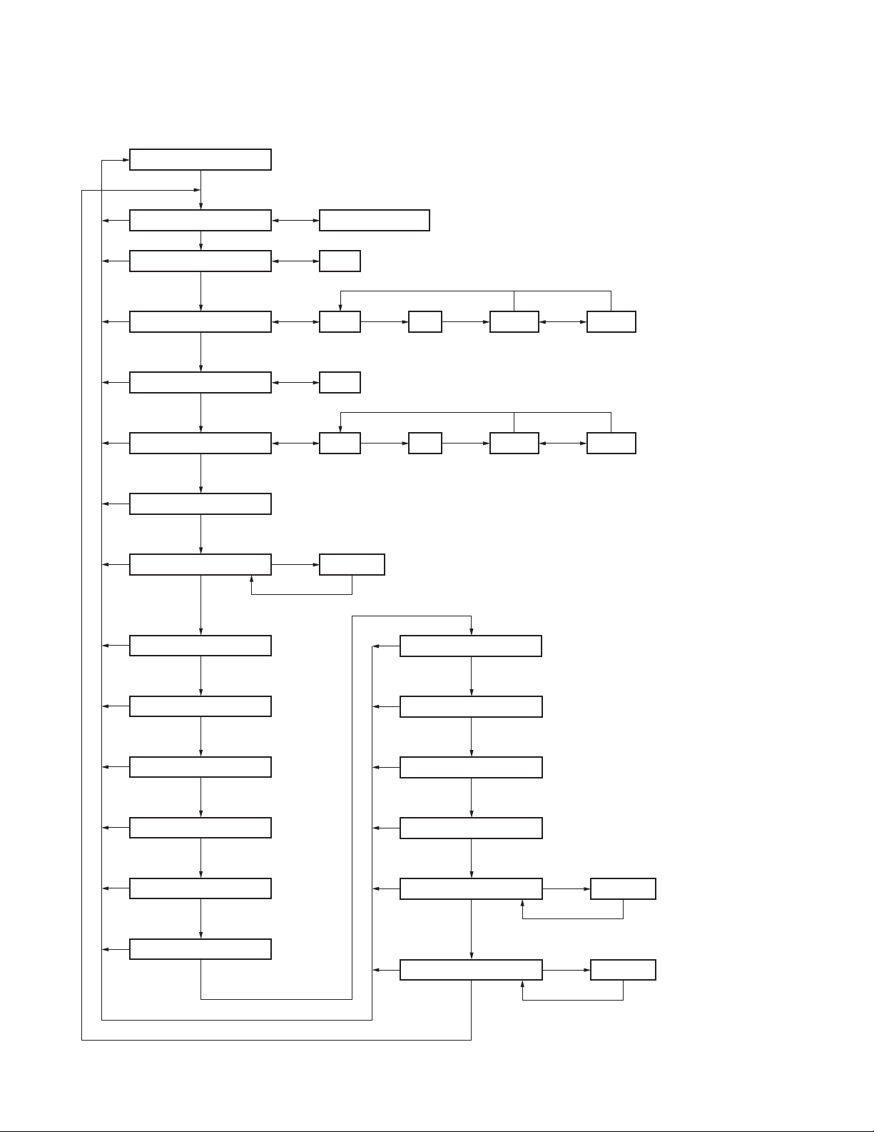
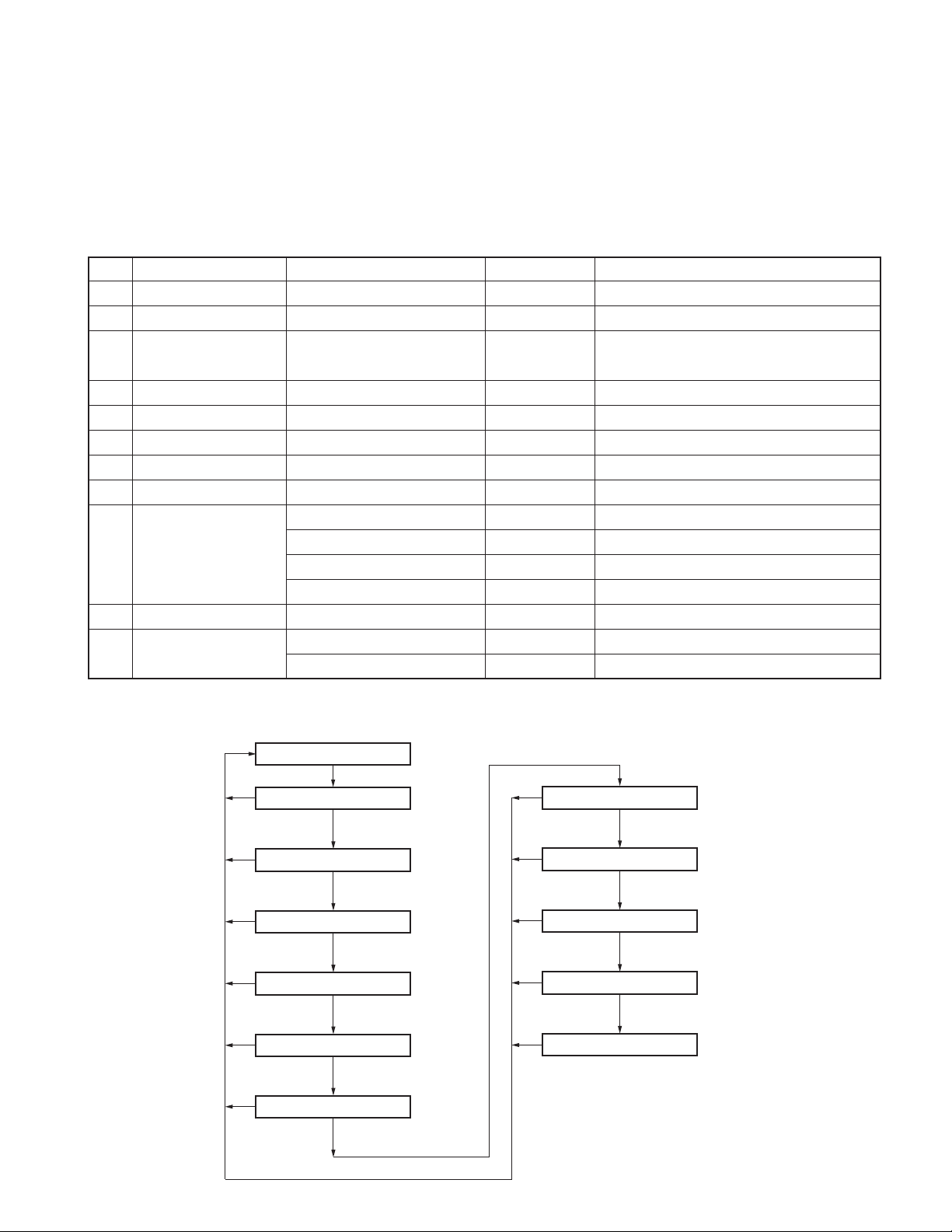
■ Channel edit mode flow chart
Self programming mode
[Side2]
DIRCT _NO
DIRCT __1
PR I _ADDR
___12345
___52134
Display when a code is input
[S]
Channel select mode Zone select mode
[S]
[S]
[S]
[S]
[S]
[S]
[S]
[S]
[S]
System reference
Transmit power
Wide 5k/Wide 4k/Narrow
Busy channel lockout
Scan delete/add
[C]
RX frequency
[B] (Write data)
[C] (Don’t write data)
RX signaling
[B] (Write data)
[C] (Don’t write data)
TX frequency
[B] (Write data)
[C] (Don’t write data)
TX signaling
[B] (Write data)
[C] (Don’t write data)
[B] (Write data)
[C] (Don’t write data)
[B] (Write data)
[C] (Don’t write data)
[B] (Write data)
[C] (Don’t write data)
[B] (Write data)
[C] (Don’t write data)
[B] (Write data)
[C] (Don’t write data)
[A]
[Side1]
[Side1] [Side1] [Side2][Side1]
[Side1]
[Side1] [Side1] [Side2][Side1]
Blank
Blank DQT N DQT IQT
Blank
Blank DQT N DQT IQT
[S]
[S]
[S]
[S]
[S]
[S]
[Side1]
[Side1]
Beat shift
[B] (Write data)
[C] (Don’t write data)
Compander
[B] (Write data)
[C] (Don’t write data)
Priority channel
[B] (Write data)
[C] (Don’t write data)
Home channel
[B] (Write data)
[C] (Don’t write data)
Direct channel
[B] (Write data)
[C] (Don’t write data)
Primary address
[B] (Write data)
[C] (Don’t write data)
Not used when Direct CH/GID
is not set in Key Assignment
8
TK-3170
Self programming mode
Channel select mode
Zone select mode
Tim e-out timer
TOT pre-alert
TOT rekey time
TOT reset time
[Side2]
[A]
[C]
[B] (Write data)
[C] (Don’t write data)
[B] (Write data)
[C] (Don’t write data)
[B] (Write data)
[C] (Don’t write data)
[B] (Write data)
[C] (Don’t write data)
[S]
[S]
[S]
[S]
[S]
[S]
You cannot enter the zone edit mode
when channel data is not set
REALIGNMENT (Signaling type for Decode = 5-tone)
■ Zone edit mode
1. Press the [A] key so that the “▼“ indicator is located on
the left side, above the zone number.
2. Rotate the selector select your desired zone number.
3. Press the [C] key to enter Zone Edit Mode.
4. Press the [C] key again to select the setting you wish to
modify.
5. Rotate the selector to select the desired value.
6. Press the [B] key to store the value in memory and advance to the next setting.
7. Press the [C] key to skip any settings you do not wish to
modify.
Press the [S] key to exit. “SELF” appears on the display.
■ Zone edit mode flow chart
No. Function Choices Display Remarks
Zone Edit
1 Time-out Timer 15~1200/15s Default=60
2 TOT Pre-alert Off, 1~10/1s Default=Off
3 TOT Rekey Time Off, 1~60/1s Default=Off
4 TOT Reset Time Off, 1~15/1s Default=Off
TOT __ _60
TOTP_OF F
TOTK_OF F
TOTS_OF F
9
TK-3170
REALIGNMENT (Signaling type for Decode = FleetSync/DTMF)
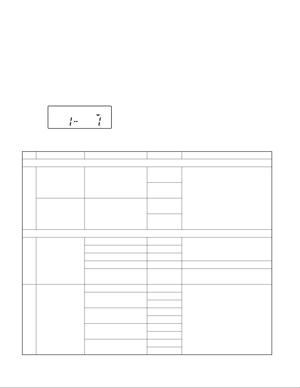
8-3. Zone/Channel Select Mode
■ To enable Zone/Channel select mode
1. Press the [Side2] key when “SELF” is displayed. The
transceiver enters Channel Select Mode. On the left half
of the display, the zone number is displayed. On the right
half of the display, the channel number is displayed.
2. Each press of the [A] key changes the position of the “▼“
indicator between the zone select (left side) and the channel select (right side).
3. Rotate the selector to set the zone or channel number,
depending on the location or the ”▼“ indicator.
■ Channel edit mode
1. Press the [A] key so that the “▼“ indicator is located on
the right side, above the channel number.
2. Rotate the selector select your desired channel number.
3. Press the [C] key to enter Channel Edit Mode.
4. Press the [C] key again to select the setting you wish to
modify.
5. Rotate the selector to select the desired value.
6. Press the [B] key to store the value in memory and advance to the next setting.
7. Press the [C] key to skip any settings you do not wish to
modify.
8. Press the [S] key to exit. “SELF” appears on the display.
No. Function Choices Display Remarks
Zone/Channel Setting Mode
Select Channel 1-128
1- 1
[A] : Zone Selection/Channel Selection change
▼
Select Zone 1-128
128 - 1
Channel Edit
1 RX Frequency Step 5.0kHz Display when an item is selected or when a step
Step 6.25kHz is changed (about 0.5 seconds)
Step 1MHz [A] : Step change, Default=6.25kHz
Blank [Side1] : Freq On/Blank switching
327.0000~550.0000MHz The rightmost dot indicates
2 RX Signaling OFF [Side1] : Off/QT/DQT switching
QT 67.0~250.3Hz [A] : Mode switching
(EIA Mode) [Side2] : Normal/Inverse switching
QT 67.0~254.1Hz Default=OFF
(0.1Hz Step Mode)
DQT 023~754 Normal
(Standard Table Mode)
DQT 000~777 Normal
(1 Step Mode)
STP__500
STP__625
STP___1M
R.– – –––––
R.4 5 0. 0000
––––––––
QT _ _ 6 7.0 _
QT _ 25 0.3_
QT _ _ 6 7.0 ∗
QT _ 25 4.1 ∗
DQT 0 2 3 N _
DQT 7 5 4 N _
DQT 0 0 0 N∗
DQT 7 7 7 N∗
▼
1-128
▼
1- 1
▼
50Hz digit (On=5; Off=0)
10

TK-3170
REALIGNMENT (Signaling type for Decode = FleetSync/DTMF)
No. Function Choices Display Remarks
DQT 023~754 Inverse
(Standard Table Mode
DQT 000~777 Inverse
(1 Step Mode)
3 TX Frequency Step 5.0kHz Same as RX frequency
Step 6.25kHz
Step 1MHz
Blank Same as RX frequency
327.0000~550.0000MHz Same as RX frequency
4 TX Signaling OFF Same as RX signaling
QT 67.0~250.3Hz
(EIA Mode)
QT 67.0~254.1Hz
(0.1Hz Step Mode)
DQT 023~754 Normal
(Standard Table Mode)
DQT 000~777 Normal
(1 Step Mode)
DQT 023~754 Inverse
(Standard Table Mode)
DQT 000~777 Inverse
(1 Step Mode)
5 Option Signaling OFF ←Default
DTMF
FleetSync
6ID DTMF Signaling = Code SQ Display when an item is selected
000~9999999999 (about 0.5 seconds)
DTMF Signaling = Selective Call Display of the current setting
000~9999 (If it is 8 or more digits, scroll it)
Code Default [Side1] : Data clear
7 Transmit Power High Transmit Power ←Default
Low Transmit Power
8 Wide 5k/Wide 4k/Narrow Wide 5k ←Default
Wide 4k
Narrow
9 Busy Channel Lockout No ←Default
QT/DQT Tone
DQT 0 2 3 I _
DQT 7 5 4 I _
DQT 0 0 0 I ∗
DQT 7 7 7 I ∗
STP__500
STP__625
STP___1M
T.– – –––––
T.4 5 0. 0 0 00
––––––––
QT _ _ 6 7.0_
QT _ 25 0.3_
QT _ _ 6 7.0∗
QT _ 25 4.1∗
DQT 0 2 3 N_
DQT 7 5 4 N_
DQT 0 0 0 N∗
DQT 7 7 7 N∗
DQT 0 2 3 I _
DQT 7 5 4 I _
DQT 0 0 0 I ∗
DQT 7 7 7 I ∗
OP _OFF _ _
OP _DTMF _
OP _ FLSY_
___ ID___
12345678
–––––123
_____000
PWR _ H ___
PWR _ L ___
WI DE_ ___
WI DE_ 4K _
NARROW_ _
BCL _NO_ _
BCL _QT _ _
Display when a code is input
(Input it with DTMF key)
11

TK-3170
REALIGNMENT (Signaling type for Decode = FleetSync/DTMF)
No. Function Choices Display Remarks
Option Signaling
Carrier Only
10 Scan Delete/Add Add ←Default
Delete
11 Beat Shift NO ←Default
YES
12 Compander NO ←Default
YES
13 Priority Channel NO ←Default
YES
14 Home Channel NO Current zone outside cannot be set up
YES Default=NO
15 Direct Channel NO Default=NO
1~4 Display when Direct CH is programmed
16 PTT ID OFF Default=OFF
Beginning of Transmit
End of Transmit
Both
17 Beginning of Transmit Code which it can input, 0~9, Not display if Dial ID =Uncheck and PTT ID=OFF,
A~D, ∗ and #, maximum of or EOT is set
16 digits. Display of the current setting
Blank [Side1] : Data clear
18 End of Transmit Code which it can input, 0~9, Not display if Dial ID =Uncheck and PTT ID=OFF,
A~D, ∗ and #, maximum of or EOT is set
16 digits. Display of the current setting
Blank [Side1] : Data clear
BCL _OPT_
BCL _CARR
S CAN_ADD
S CAN_DE L
SHF T _NO_
SHF T _YES
COMP _ NO_
COMP _ Y E S
P RCH_NO_
P RCH_YES
HMC H _ NO _
HMC H _ Y E S
DIRCT _NO
DIRCT __1
PID_OFF_
PID_BOT_
PID_EOT_
PID_BOTH
BOT _ I D _ _
12345678
–––––987
––––––––
EOT _ I D_ _
12345678
–––––987
––––––––
Display when Direct CH is programmed
(If it is 8 or more digits, scroll it)
Display when a code is input
(Input it with DTMF key)
(If it is 8 or more digits, scroll it)
Display when a code is input
(Input it with DTMF key)
12
TK-3170
REALIGNMENT (Signaling type for Decode = FleetSync/DTMF)
■ Channel edit mode flow chart
Self programming mode
[Side2]
[S]
Channel select mode Zone select mode
[S]
[S]
[S]
[S]
[S]
[S]
[S]
[S]
[S]
[S]
[S]
[S]
Option signaling
Transmit power
Wide 5k/Wide 4k/Narrow
Busy channel lockout
Scan delete/add
[C]
RX frequency
[B] (Write data)
[C] (Don’t write data)
RX signaling
[B] (Write data)
[C] (Don’t write data)
TX frequency
[B] (Write data)
[C] (Don’t write data)
TX signaling
[B] (Write data)
[C] (Don’t write data)
[B] (Write data)
[C] (Don’t write data)
ID
[B] (Write data)
[C] (Don’t write data)
[B] (Write data)
[C] (Don’t write data)
[B] (Write data)
[C] (Don’t write data)
[B] (Write data)
[C] (Don’t write data)
[B] (Write data)
[C] (Don’t write data)
Beat shift
[B] (Write data)
[C] (Don’t write data)
Compander
[B] (Write data)
[C] (Don’t write data)
[A]
[Side1]
[Side1] [Side1] [Side2][Side1]
[Side1]
[Side1] [Side1]
[Side1]
Blank
Blank DQT N DQT IQT
Blank
Blank DQT N DQT IQT
Default ID
[S]
[S]
[S]
[S]
[S]
[S]
[Side1]
[Side1]
Priority channel
[B] (Write data)
[C] (Don’t write data)
Home channel
[B] (Write data)
[C] (Don’t write data)
Direct channel
[B] (Write data)
[C] (Don’t write data)
PTT ID
[B] (Write data)
[C] (Don’t write data)
Beginning of TX
[B] (Write data)
[C] (Don’t write data)
End of TX
[Side2][Side1]
Not used when Direct CH/GID
is not set in Key Assignment
[Side1]
[Side1]
Data clear
Data clear
Not valid if Dail ID=Disable
and PTT ID=off, or EOT
is set
Not valid if Dail ID=Disable
and PTT ID=off, or EOT
is set
[B] (Write data)
[C] (Don’t write data)
13
TK-3170
Self programming mode
Channel select mode
Zone select mode
Tim e-out timer
TOT pre-alert
TOT rekey time
TOT reset time
Option signaling
decode condition
Audio control
[Side2]
[A]
[C]
[B] (Write data)
[C] (Don’t write data)
[B] (Write data)
[C] (Don’t write data)
[B] (Write data)
[C] (Don’t write data)
[B] (Write data)
[C] (Don’t write data)
[B] (Write data)
[C] (Don’t write data)
[B] (Write data)
[C] (Don’t write data)
[S]
[S]
[S]
[S]
[S]
[S]
[S]
[S]
You cannot enter the zone edit mode
when channel data is not set
REALIGNMENT (Signaling type for Decode = FleetSync/DTMF)
■ Zone edit mode
1. Press the [A] key so that the “▼“ indicator is located on
the left side, above the zone number.
2. Rotate the selector select your desired zone number.
3. Press the [C] key to enter Zone Edit Mode.
4. Press the [C] key again to select the setting you wish to
modify.
5. Rotate the selector to select the desired value.
6. Press the [B] key to store the value in memory and advance to the next setting.
7. Press the [C] key to skip any settings you do not wish to
modify.
Press the [S] key to exit. “SELF” appears on the display.
■ Zone edit mode flow chart
No. Function Choices Display Remarks
Zone Edit
1 Time-out Timer 15~1200/15s Default=60
2 TOT Pre-alert Off, 1~10/1s Default=Off
3 TOT Rekey Time Off, 1~60/1s Default=Off
4 TOT Reset Time Off, 1~15/1s Default=Off
5 Option Signaling Decode QT/DQT ←Default
Condition Carrier
6 Audio Control QT/DQT ←Default
14
QT/DQT and Option Signaling
QT/DQT or Option Signaling
TOT __ _60
TOTP_OFF
TOTK_OFF
TOTS_OFF
OPDC _QT _
OPDC _ CR _
ADC _QT _ _
ADC _ AND_
ADC _OR _ _
REALIGNMENT
TK-3170
8-4. Function Setting Mode
5-tone and FleetSync/DTMF common item.
1. Press the [Side1] key when “SELF” is displayed. The
transceiver enters Function Setting Mode.
2. Press the [C] key to select the setting you wish to modify.
4. Press the [B] key to store the value in memory and advance to the next setting.
5. Press the [C] key to skip any settings you do not wish to
modify.
6. Press the [S] key to exit. “SELF” appears on the display.
3. Rotate the selector to select the desired value.
No. Function Choices Display Remarks
1Auto Backlight YES/NO Default=No
2 Power-on Tone Current/Off, 1~31 Default=Current
3 Control Tone Current/Off, 1~31 During Self-Programming, it is constant
4 Warning Tone Current/Off, 1~31 Default=Current
5Alert Tone Current/Off, 1~31 Default=Current
6Side Tone Current/Off, 1~31 Default=Current
7 Minimum Volume 0~31 Default=0
8 Battery Saver ON/OFF Default=ON
9 Battery Warning Off
While Transmitting ←Default
Always
Always with Beep
10 Squelch Level 0~9/1STEP Default=5
11 Panel Test/ Enable
Panel Tuning Mode Disable ←Default
ATL T_NO_
PONT _CUR
CNT T _ CUR
Default=Current
WA R T _ C UR
ALT T_CUR
SIDT_CUR
MINI ___ 0
BAT T _ _ON
BTW_OFF_
BTW_WTX_
BTW_ALWY
BTW_ALWB
SQL _ _ _ 5 _
PTM_ENA_
PTM_D I S_
■ Function setting mode flow chart
Self programming mode
[S]
[S]
[S]
[S]
[S]
[S]
Auto backlight
Power-on tone
[Side1]
[B] (Write data)
[C] (Don’t write data)
[B] (Write data)
[C] (Don’t write data)
Control tone
[B] (Write data)
[C] (Don’t write data)
Warning tone
[B] (Write data)
[C] (Don’t write data)
Alert tone
[B] (Write data)
[C] (Don’t write data)
Side tone
[B] (Write data)
[C] (Don’t write data)
[S]
[S]
[S]
[S]
[S]
Minimum volume
[B] (Write data)
[C] (Don’t write data)
Battery saver
[B] (Write data)
[C] (Don’t write data)
Battery warning
[B] (Write data)
[C] (Don’t write data)
Squelch level
[B] (Write data)
[C] (Don’t write data)
Panel test/Panel tuning mode
15
TK-3170
REALIGNMENT / DISASSEMBLY FOR REPAIR
8-5. Memory Reset Mode
• This mode is used to clear data for functions that can be
set in Self-Programming Mode or to return to reset values
(default).
• Pressing [S] key when “SELF” is shown, sets the display
to “CANCEL”.
• Turning the selector alternately switches the display between “CANCEL” ↔ “READY”.
• Pressing [B] key when “READY” is shown, clears the data
and sets the display to “CLEAR”.
• Pressing [S] key again, returns the display to “SELF”.
• Pressing [S] key when “CANCEL” is shown, returns the
display to “SELF” without resetting the data.
9. Firmware Version Information Mode
Turn the transceiver ON with the [Side1] key held down.
Then, the version is displayed during holding the [Side1] key.
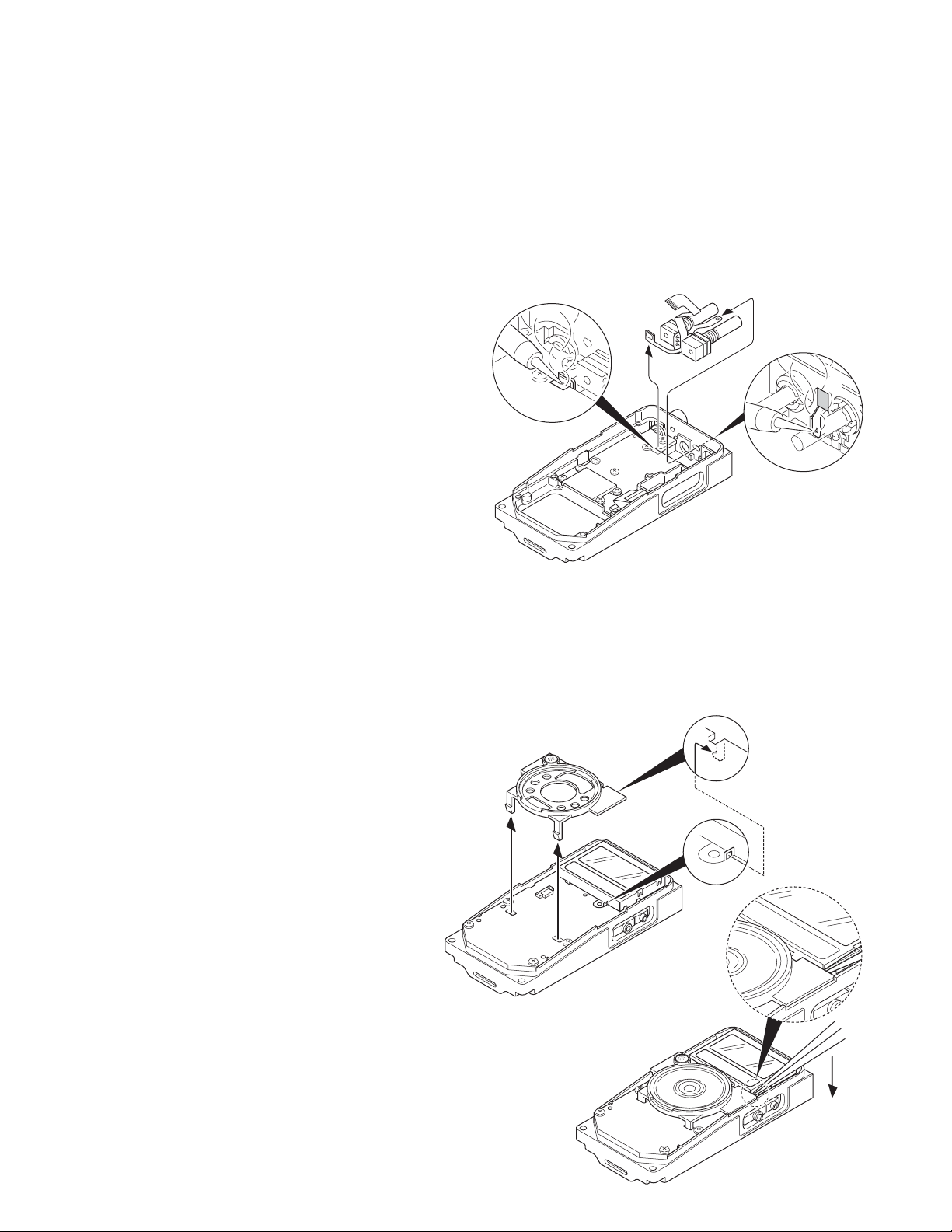
1. Removing the FPC
1) Remove the solder from the TX-RX unit using a solder iron
( q ).
2) Peel the double-sided tape ( w ).
3) Remove the solder from the battery terminal block using
the solder iron ( e ).
Note : You must replace the FPC and the double-sided tape
(4 x 7 mm) when replacing the volume or the selector.
w
q
e
2. Separating the Speaker Holder from the Control Unit
1) As in shown in the figure below, the speaker holder is at-
tached to the LCD cover with tab ( q ).
Use a pair of tweezers or similar instrument to lift the
speaker holder away from the control unit ( w ).
q
16
w
DISASSEMBLY FOR REPAIR
TK-3170
3. How to Assemble the Antenna Connector and its Terminal
The antenna connector and its terminal are supplied as
separate parts.
When replacing the antenna connector and/ or terminal,
assemble the parts prior to the replacement.
1) Mount the antenna connector onto the chassis ( q ).
Double-sided tape is attached to the terminal; peel off the
tape cover ( w ).
Attach the terminal to the antenna connector as shown
below.
Slide the antenna terminal along the adhesive cushion on
the chassis so that the adhesive part on the terminal is
firmly attached to the antenna connector ( e ).
2) Remove the antenna connector from the chassis with its
terminal attached, then solder the center part of antenna
connector to its terminal ( r ).
Do not use excessive solder on terminal.
TOP
w
Bottom
q
4. How to Apply the Double-Sided tape
Position the edge of the double-sided tape so that it is in
the center of the hole in the chassis.
Double-sided tape
(J99-0399-04)
FPC
Hole of chassis
5. How to Apply the Fibrous Sheet
Align the fibrous sheet at position “A” in the illustration.
Apply the fibrous sheet so that it does not protrude from
the casing.
Position line “A”
Fibrous sheet
(G10-1304-04)
Cushion
e
6. How to Mount the LCD Fixture
When mounting the LCD fixture onto the PCB, ensure that
it is aligned parallel to the chassis.
r
LCD fixture
Chassis
17
TK-3170
DISASSEMBLY FOR REPAIR
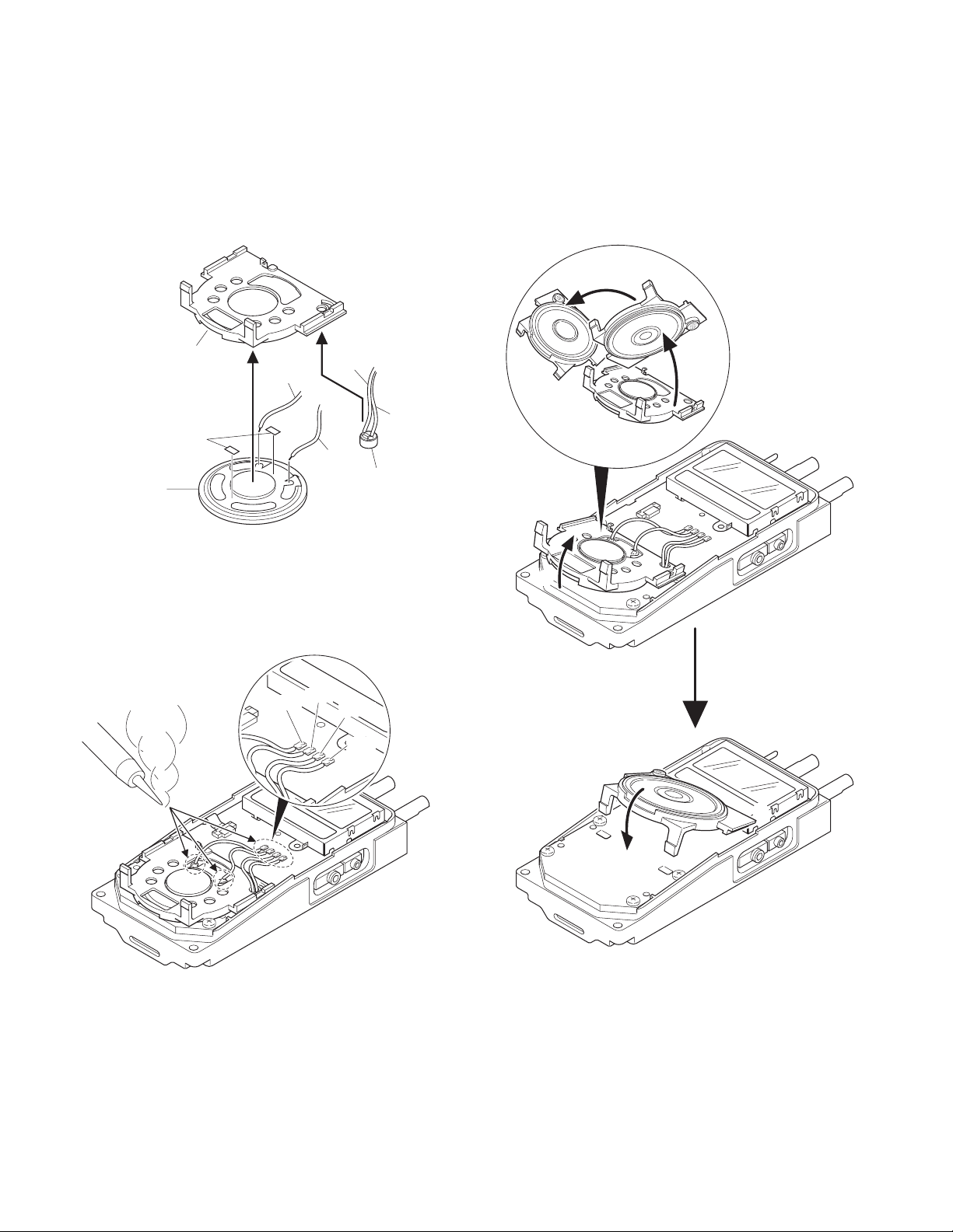
7. Replacing the Speaker and Microphone
1) After affixing the double-sided tape (5.4 x 2.7 mm) to the
speaker, attach the speaker to the speaker holder ( q ).
2) Insert the microphone into the hold of the holder, as
shown by the diagram ( w ).
Speaker holder
Black
q
Double-sided tape
Speaker
3) Match the speaker and microphone lead wires with the
color-code of silkscreen of the printed circuit board ( e ),
then solder them in place.
w
White
Blue
Red
Microphone
4) Lift the speaker holder ( r ), then flip it over to the left
( t ).
5) Insert the tabs of the speaker holder into the slots of the
transceiver.
First insert the bottom tabs into the control unit ( y ), then
insert the top tabs into the LCD cover ( u ).
t
r
e
Black
Red
White
Blue
u
y
18
CIRCUIT DESCRIPTION
MXO
AFOUT
QUAD
IFOUT
IFI
Wide5k, Wide 4k
C702
C701
C708
C719
R705
R702
R701
R703
R706
C709
R708
D702 D701
CF701
CF702
IC701
R719
R717
Q702
R718
5C
AFOUT
Narrow
Narrow
CD701
TK-3170
1. Frequency Configuration
The receiver utilizes double conversion. The first IF is
49.95MHz and the second IF is 450kHz. The first local oscillator signal is supplied from the PLL circuit.
The PLL circuit in the transmitter generates the necessary
frequencies. Figure 1 shows the frequencies.
TX/RX : 440~470MHz (E)
470~512MHz (X2)
ANT
1st MIX
ANT
SW
AMP
RF
AMP
q
TX
440~470MHz (E)
470~512MHz (X2)
MCF
49.95MHz
RF
AMP
q
CF
450kHz
IF
SYSTEM
X3
multiply
PLL
VCO
390.05~420.05MHz (E)
420.05~462.05MHz (X2)
VOL
50.4MHz
TCXO
AF
AMP
16.8MHz
MIC
AMP
SP
MIC
Fig. 1 Frequency configuration
2. Receiver System
The receiver system is shown in Figure 2.
The filtered first IF signal is amplified by the first IF amplifier
(Q703) and then applied to the lF system IC (IC701). The IF
system IC provides a second mixer, second local oscillator,
limiting amplifier, quadrature detector and RSSI (Received
Signal Strength Indicator). The second mixer mixes the first
IF signal with the 50.4MHz of the second local oscillator output (TCXO X501) and produces the second IF signal of
450kHz.
The second IF signal is passed through the ceramic filter
(Wide 5k, Wide 4k : CF701, Narrow : CF702) to remove the
adjacent channel signal. The filtered second IF signal is amplified by the limiting amplifier and demodulated by the
quadrature detector with the ceramic discriminator (CD701).
The demodulated signal is routed to the audio circuit.
2-4. Wide 5k, Wide 4k/Narrow Switching Circuit
Wide 5k, Wide 4k and Narrow settings can be made for
each channel by switching the ceramic filters CF701 (Wide
5k, Wide 4k), CF702 (Narrow). The Wide 5k, Wide 4k and
Narrow switching data is output from IC4.
D701 and D702 are switched to ceramic filters when a
Wide 5k, Wide 4k/Narrow level is selected.
Q702 turns on/off with the Narrow and the IC701 detector
output level is changed to maintain a constant output level
during wide or narrow signals.
2-1. Front End (RF AMP)
The signal coming from the antenna passes through the
transmit/receive switching diode circuit (D604, D605, D606
and D608), passes through a BPF (L717 and L718), and is
amplified by the RF amplifier (Q705).
The resulting signal passes through a BPF (L711, L712 and
L713) and goes to the mixer. These BPFs are adjusted by
variable capacitors (D703, D704, D705, D706 and D707). The
input voltage to the variable capacitor is regulated by voltage
output from the DC amplifier (IC19).
2-2. First Mixer
The signal from the front end is mixed with the first local
oscillator signal generated in the PLL circuit by Q704 to produce a first IF frequency of 49.95 MHz.
The resulting signal passes through the XF701 MCF to cut
the adjacent spurious and provide the optimum characteristics, such as adjacent frequency selectivity.
2-3. IF Amplifier Circuit
The first IF signal is passed through a four-pole monolithic
crystal filter (XF701) to remove the adjacent channel signal.
ANT
ANT
SW
Q705
RF
AMP
BPF
TUNE TUNE
BPF
Q704
1st MIX
1st Local
XF701
MCF
Fig. 2 Receiver system
Q703
IF AMP
Fig. 3 Wide 5k, Wide 4k/Narrow switching circuit
CF702
CF701
IC701
IF, MIX, DET
Q701
X3 multiply
2nd Local
IC10
AF AMP
X501
TCXO
16.8MHz
IC13
AQUA-L
IC16
VOL
IC18
AF PA
SP
19
TK-3170
CIRCUIT DESCRIPTION
2-5. Audio Amplifier Circuit
The demodulated signal from IC701 is amplified by IC10,
and goes to AF amplifier through IC13.
The signal then goes through an volume control (IC16),
and is routed to an audio power amplifier (IC18) where it is
amplified and output to the speaker.
2-6. Squelch Circuit
Part of the AF signal from the IC enters the FM IC (IC701)
again, and the noise component is amplified and rectified by a
filter and an amplifier to produce a DC voltage corresponding
to the noise level.
The DC signal from the FM IC goes to the analog port of
the microprocessor (IC7). IC7 determines whether to output
sounds from the speaker by checking whether the input voltage is higher or lower than the preset value.
To output sounds from the speaker, IC7 sends a high sig-
nal to the AM2 line and IC5 sends a high signal to the AM1
line, and turns IC18 on through Q23, Q24, Q27, Q28 and
Q35. (See Figure 4)
IC701
FM IF
ANSQL
IC7
CPU
IC5
Shift register
LSDI
HSDI
AM2
AM1
IC10
IF AMP
SIGNAL
DTMF
QT/DQT
CLK, DATA,STD, LOADN
IC15
BPF & Compalater
Q22
SW
AF PA
IC16
VOL
Q23,24,27
IC11
LPF
IC18
SW
AQUA-L
5-tone
Q28,35
SW
IC13
Fig. 4 Audio amplifier and squelch circuit
3. Transmitter System
3-1. Microphone Amplifier
The signal from microphone amplified by IC13 (1/2) and
limited by AGC circuit composed of D30, D31, Q25 and Q26,
and goes through mute switch (Q30). IC13 is composed of
high-pass filter, low-pass filter and pre-emphasis/IDC circuit.
The signal enters the summing amplifier consisting of
IC12 (2/2), and passes through the D/A converter (IC16) for
the maximum deviation adjustment, and is mixed with the
low speed data from the CPU (IC7).
The output signal from the D/A converter goes to the VCO
modulation input. The other output signal from the D/A converter passes through the D/A converter (IC16) again for the
BAL adjustment, and the buffer amplifier (IC17), and goes to
the TCXO modulation input.
20
SP
IC13
(1/2)
MIC Q30
AMP
AGC
D30,31
Q25,26
IC16
I2
D/A
SW
MMUTE
O2
IC13
AQUA-L
O8
IC17 X701
BUFF
AMP
IC16
I8
D/A
LSD
OUT
IC12
(2/2)
SUM
AMP
VCO
TCXO
Fig. 5 Microphone amplifier
3-2. Drive and Final Amplifier
The signal from the T/R switch (D516 is on) is amplified by
the pre-drive (Q602) and drive amplifier (Q603) to 50mW.
The output of the drive amplifier is amplified by the RF
final amplifier (Q604) to 4.0W (1W when the power is low).
The RF final amplifier consists of two MOS FET stages.
The output of the RF final amplifier is then passed through
the harmonic filter (LPF) and antenna switch (D604 and D605)
and applied to the antenna terminal.
3-3. APC Circuit
The APC circuit always monitors the current flowing
through the RF power amplifier (Q604) and keeps a constant
current. The voltage drop at R621, R623 and R629 is caused
by the current flowing through the RF final amplifier and this
voltage is applied to the differential amplifier IC601(1/2).
IC601(2/2) compares the output voltage of IC601(1/2) with
the reference voltage from IC7. The output of IC601(2/2)
controls the VG of the RF power amplifier, drive amplifier and
pre-drive amplifier to make both voltages the same.
The change of power high/low is carried out by the change
of the reference voltage.
ANT
LPF
From
T/R SW
(D516)
+B
PC
(IC7)
Q601
RF
AMP
Q602 Q603
Pre-
DRIVE
AMP
R621
R623
R629
DRIVE
AMP
Q604
RF
FINAL
AMP
VDD VG
IC601
(1/2)
D604,605
ANT
SW
IC601
(2/2)
Fig. 6 Drive and final amplifier and APC circuit
CIRCUIT DESCRIPTION
TK-3170
4. Frequency Synthesizer Unit
4-1. Frequency Synthesizer
The frequency synthesizer consists of the TCXO (X501),
VCO, PLL IC (IC501) and buffer amplifiers.
The TCXO generates 16.8MHz. The frequency stability is
2.5ppm within the temperature range of –30 to +60°C. The
frequency tuning and modulation of the TCXO are done to
apply a voltage to pin 1 of the TCXO. The output of the TCXO
is applied to pin 8 of the PLL IC.
The VCO consists of 2VCO and covers a dual range of the
390.05~420.05MHz (E) or 420.05~462.05MHz (X2) and the
440~470MHz (E) or 470~512MHz (X2). The VCO generates
390.05~420.05MHz (E) or 420.05~462.05MHz (X2) for providing to the first local signal in receive. The operating frequency is generated by Q502 in transmit mode and Q503 in
receive mode. The oscillator frequency is controlled by applying the VCO control voltage, obtained from the phase comparator (IC501) to the variable capacitor diodes (D505 and
D507 in transmit mode and D509 and D511 in receive mode).
The RX pin of IC4 goes “low” in receive mode causing
Q503 and Q504 (2/2) turn on. The TX pin goes “low” in transmit mode causing Q502 and Q504 (1/2) turn on.
The outputs from Q502 and Q503 are amplified by buffer
amplifier (Q506) and doubled by Q501 and then sent to PLL
IC.
The PLL IC consists of a prescaler, reference divider,
phase comparator, charge pump (The frequency step of the
PLL circuit is 5 or 6.25kHz). The input signal from the pins 8
and 5 of the PLL IC is divided down to the 5 or 6.25kHz and
compared at phase comparator. The pulsed output signal of
the phase comparator is applied to the charge pump and
transformed into DC signal in the loop filter (LPF). The DC
signal is applied to the CV of the VCO and locked to keep the
VCO frequency constant.
PLL data is output from PLLDAT (pin 93), PCK (pin 79) and
PLE (pin 78) of the microprocessor (IC7). The data are input
to the PLL IC when the channel is changed or when transmission is changed to reception and vice versa. A PLL lock condition is always monitored by the pin 77 (UL) of the microprocessor. When the PLL is unlocked, the UL goes low.
SW
To mixer
VC
D516
SW
D515
IC17
To
drive
amp
FC
BAL
TX
RX
Q507
RFVCO
CV
LPF
IC501
20
PLL
15
UL
CPU
PLLDT,PCK,PLE
IC7
Q501
Doubler
x2
5
8
TCXO
X501
Fig. 7 PLL block diagram
5. Control Circuit
The control circuit consists of microprocessor (IC7) and its
peripheral circuits. It controls the TX-RX unit. IC7 mainly performs the following;
1) Switching between transmission and reception by PTT
signal input.
2) Reading system, zone, frequency, and program data from
the memory circuit.
3) Sending frequency program data to the PLL.
4) Controlling squelch on/off by the DC voltage from the
squelch circuit.
5) Controlling the audio mute circuit by decode data input.
6) Transmitting tone and encode data.
5-1. Frequency Shift Circuit
The microprocessor (IC7) operates at a clock of 11.0592
MHz. This oscillator has a circuit that shifts the frequency by
Beat shift switch (Q17).
A beat sound may be able to be evaded from generation if
“Beat Shift” is set to ON when it is generated in the internal
spurious transmission modulated sound of a transceiver.
XIN
Q17
IC7
CPU
XOUT
SHIFT
C62 X1
Fig. 8 Frequency shift circuit
5-2. Memory Circuit
Memory circuit consists of the CPU (IC7) and a flash
memory (IC8). A flash memory has a capacity of 4M bits and
contains the transceiver control program for the CPU. It also
stores the data for transceiver channels and operating parameter that are written by the FPU. This program can be easily
written from an external devices.
The EEPROM (IC9) stores the last channel data, the scan
on status, and other parameters.
■ Flash memory
Note : The flash memory stores the data that is written by
the FPU (KPG-101D), and firmware program (User mode,
Test mode, Tuning mode, etc.). This data must be rewritten
when replacing the flash memory.
■ EEPROM
Note : The EEPROM stores tuning data (Deviation, Squelch,
etc.).
Realign the transceiver after replacing the EEPROM.
IC8
IC7
CPU
“H” : OFF
“L” : ON
IC9
EEPROMFLASH
Fig. 9 Memory circuit
21
 Loading...