

Page 1
PARTS LIST
TK-3140
CAPACITORS
1 = Type ... ceramic, electrolytic, etc.
2 = Shape ... round, square, ect.
3 = Temp. coefficient
Temperature coefficient
1st Word
Color*
ppm/
Tolerance (More than 10pF)
Code
(%)
Voltage rating
1st word
Black Red Orange Yellow Green Blue Violet
0 -80 -150 -220
C
0.25 0.5 2 5 10 20
2nd word
0
1
2
3
CC 45
1
1
2
LCPRSTU
DGJKMXZP
BCDEF
A
1.0
1.25
10
12.5
100
125
1000
1250
TH 1H J220
3
4
5
4 = Voltage rating
5 = Value
6 = Tolerance
2.0
1.6
20
16
200
160
2000
1600
6
-330 -470 -750
+ 40
+ 80
- 40
- 20
3.15
2.5
31.5
25
315
250
3150
2500
CC45
+ 100
-0
G
4.0
40
400
4000
Color*
2nd Word HG
ppm/
Example : CC45TH = -470
No code
More than 10µF -10 +50
Less than 4.7µF-10 +75
H
J
5.0
6.3
50
63
500
630
5000
6300
Capacitor value
010 = 1pF
100 = 10pF
101 = 100pF
102 = 1000pF = 0.001µF
103 = 0.01µF
30 60
K
V
8.0
-
80
35
800
-
8000
-
22
JKL
120 250 500
60ppm/
(Less than 10pF)
Gode
(pF)
CDFGB
0.1 0.25 0.5 1 2
0 = 22pF
Multiplier
2nd number
1st number
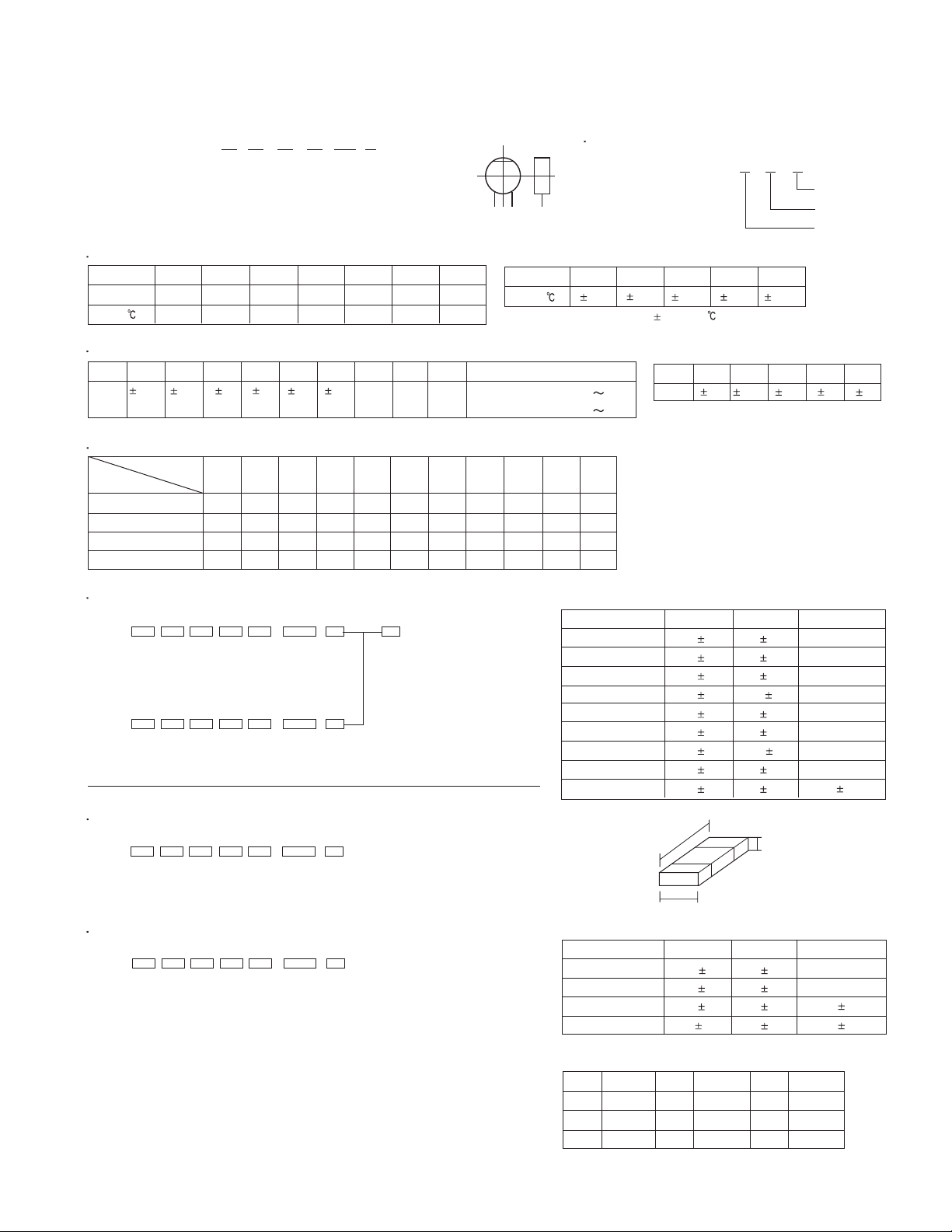
Chip capacitors
(EX) C C 7 3 F S L 1 H
(Chip)(CH,RH<UJ,SL)
(EX) C K 7 3 F F 1 H
(Chip)(B,F)
RESISTORS
Chip resistor (Carbon)
(EX) R K 7 3 E B 2 B
(Chip)(B,F)
Carbon resistor (Nomal type)
(EX) R D 1 4 B B
1 = Type
2 = Shape
3 = Dimension
4 = Temp. coefficient
2C
000
000
000
000
J
7654321
Z
7654321
J
7654321
J
7654321
5 = Rating wattage
6 = Value
7 = Tolerance
Refer to the table above.
1 = Type
2 = Shape
3 = Dimension
4 = Temp. coefficient
5 = Voltage rating
6 = Value
7 = Tolerance
Dimension (Chip capacitors)
Dimension code L W T
Empty
A
B
C
D
E
F
G
H
Dimension
Dimension (Chip resistor)
Dimension code L W T
E
F
G
H
Rating wattage
Wattage
Code
1/16W
1J
1/10W
2A
1/8W
2B
5.6
4.5
4.5
4.5
3.2
3.0
2.0
1.6
1.0
W
3.2
2.0
1.6
1.0
Code
2C
2E
2H
L
0.5
0.5
0.5
0.5
0.4
0.2
0.3
0.2
0.05
0.2
0.3
0.2
0.05
Wattage
1/6W
1/4W
1/2W
5.0
3.2
2.0
1.25
2.5
1.6
1.25
0.8
0.5
1.6
1.25
0.8
0.5
Code
0.5
0.4
0.3
0.2
0.3
0.2
0.2
0.2
0.05
T
0.2
0.2
0.2
0.05
3A
3D
Less than 2.0
Less than 2.0
Less than 2.0
Less than 1.25
Less than 1.5
Less than 1.25
Less than 1.25
Less than 1.0
0.5
0.5
0.35
Wattage
1W
2W
0.05
1.0
1.0
0.1
0.05
25
Page 2
TK-3140
New Parts. indicates safety critical components.
∗
Parts without Parts No. are not supplied.
Les articles non mentionnes dans le Parts No. ne sont pas fournis.
Teile ohne Parts No. werden nicht geliefert.
TK-3140 (Y50-5642-XX)
TX-RX UNIT (X57-6412-XX)
Ref. No. Parts No. Description
11B∗ A02-3653-14 CABINET ASSY(4 KEYS)
23A∗ A10-4063-01 CHASSIS
Address
New
parts
TK-3140
PARTS LIST
L:
Scandinavia
Y:
PX (Far East, Hawaii)
Y:
AAFES (Europe)
Destination Destination
Ref. No.
F3BN79-2035-46
G1AN83-2005-46 PAN HEAD TAPTITE SCREW(UNIT)
60 2B R31-0617-05 VARIABLE RESISTOR(POWER SW/VOL)
Address
K:
New
parts
USA
T:
England
X:
Australia
P:
Canada
E:
Europe
M:
Other Areas
Parts No. Description
PAN HEAD TAPTITE SCREW(TERMINAL)
53B∗ B01-0694-03 ESCUTCHEON(BELT HOOK)
62CB09-0625-03 CAP ACCESSORY
72BB10-2700-02 FRONT GLASS
81AB38-0859-05 LCD ASSY
91C∗ B62-1479-00 INSTRUCTION MANUAL
10 3A ∗ B72-2106-04 MODEL NAME PLATE E
10 3A ∗ B72-2107-04 MODEL NAME PLATE E3
13 3B E04-0436-05 RF COAXIAL RECEPTACLE(SMA)
14 3A E23-1188-04 TERMINAL(ANT)
15 3A E23-1189-04 TERMINAL(BATT-)
16 2A E37-0978-05
17 3A ∗ E37-1007-05
18 3B E58-0440-05 SQUARE SOCKET(SP/MIC)
19 3A E72-0413-03 TERMINAL BLOCK(BATT)
20 2A ∗ F10-2415-04 SHIELDING PLATE(CPU)
21 1A F10-2416-03 SHIELDING PLATE(LCD)
22 2A ∗ F10-2444-04 SHIELDING PLATE(SP)
23 3B ∗ F15-1006-04 SHIELDING PLATE(CHASSIS)
24 1A F20-1192-04 INSULATING SHEET(LCD)
25 1B ∗ G10-1304-04 FIBROUS SHEET(CABINET)
26 3A G11-4046-14 SHEET(PTT)
27 2A G11-4050-04 SHEET(TCXO)
28 1A G11-4089-04 SHEET(LCD)
29 3A G11-4090-04 SHEET(FINAL FET)
30 1A ∗ G11-4174-04 SHEET(LCD)
33 1A,2A ∗ G11-4188-04 SHEET(A/3PCB,SHIELDING PLATE(LCD))
34 1B ∗ G11-4189-04 SHEET(UPPER SIDE OF CABINET)
35 1A ∗ G11-4190-04 SHEET(LOWER SIDE OF CABINET)
36 3A G13-1885-04 CUSHION(CHASSIS)
37 2B ∗ G53-1540-12 PACKING(4 KEYS)
38 3A ∗ G53-1547-04 PACKING(TERMINAL BLOCK)
39 3B ∗ G53-1560-02 PACKING(TOP)
40 1D H52-1816-02 ITEM CARTON CASE
45 2A J19-5430-03 HOLDER(VOL/ENC)
47 2A J21-8424-04 HARDWARE FIXTURE(CHASSIS)
48 2C ∗ J29-0701-05 BELT HOOK ACCESSORY
49 1B J30-1269-04 SPACER(VOL)
50 2B J82-0078-05 FPC(VOL/ENC)
51 3B J82-0079-05 FPC(UNIVERSAL)
55 1B K29-9131-03 KNOB(PTT)
56 1A K29-9132-03 KEY TOP(SW1,SW2)
57 1B K29-9133-03 KNOB(VOL)
58 1B K29-9134-03 KNOB(ENC)
A2CN08-0548-04 DRESSED SCREW ACCESSORY
B3BN14-0569-04 CIRCULAR NUT(VOL,ENC)
C3BN30-2604-46 PAN HEAD MACHINE SCREW(ANT)
D3AN30-2608-46
E3BN30-3006-45
LEAD WIRE WITH CONNECTOR(SW2,SP)
LEAD WIRE WITH CONNECTOR(SW1,PTT)
PAN HEAD MACHINE SCREW(CABINET)
PAN HEAD MACHINE SCREW(ESCUTCHEON)
61 2B S60-0415-05 ROTARY SWITCH(ENCODER)
62 1B T07-0732-05 SPEAKER
63 2D ∗ T90-0798-05 HELICAL ANTENNA E
63 2D ∗ T90-0800-05 HELICAL ANTENNA E3
64 2B T91-0630-05 MIC ELEMENT
TX-RX UNIT (X57-6412-XX) -71 : E -72 : E3
D309 B30-2156-05 LED(RED)
D310 B30-2157-05 LED(YELLOW)
C1 CK73HB1H471K CHIP C 470PF K
C2 CK73HB1H102K CHIP C 1000PF K
C4 CC73HCH1H100D CHIP C 10PF D
C5 CK73HB1H471K CHIP C 470PF K
C8 CK73HB1H102K CHIP C 1000PF K
C9 CC73HCH1H100D CHIP C 10PF D
C28 CC73HCH1H101J CHIP C 100PF J
C29 CK73HB1H102K CHIP C 1000PF K
C30 CC73HCH1H100D CHIP C 10PF D
C31 CC73HCH1H090D CHIP C 9.0PF D E
C31 CC73HCH1H200J CHIP C 20PF J E3
C32 CC73HCH1H060D CHIP C 6.0PF D
C33 CC73HCH1H150J CHIP C 15PF J E
C33 CC73HCH1H560J CHIP C 56PF J E3
C34 CC73HCH1H050C CHIP C 5.0PF C E
C34 CC73HCH1H100D CHIP C 10PF D E3
C36 CC73GCH1H030B CHIP C 3.0PF B E3
C36 CC73GCH1H3R5B CHIP C 3.5PF B E
C37 CC73GCH1H0R5B CHIP C 0.5PF B
C38 CC73GCH1H040B CHIP C 4.0PF B E
C38 CC73GCH1H050B CHIP C 5.0PF B E3
C39 CK73HB1H471K CHIP C 470PF K
C40 CC73GCH1H020B CHIP C 2.0PF B E3
C40 CC73GCH1H030B CHIP C 3.0PF B E
C41 CC73GCH1H040B CHIP C 4.0PF B E
C41 CC73GCH1H090B CHIP C 9.0PF B E3
C42 CC73GCH1H2R5B CHIP C 2.5PF B E3
C42 CC73GCH1H3R5B CHIP C 3.5PF B E
C43 CC73GCH1H0R5B CHIP C 0.5PF B
C44 CC73GCH1H040B CHIP C 4.0PF B
C45 CK73HB1H471K CHIP C 470PF K
C46 CC73HCH1H101J CHIP C 100PF J
C47 CC73GCH1H0R5B CHIP C 0.5PF B
C48,49 CK73HB1H102K CHIP C 1000PF K
C50 C92-0712-05 CHIP-TAN 22UF 6.3WV
C51 CC73HCH1H070D CHIP C 7.0PF D
C52 CK73HB1H102K CHIP C 1000PF K
C53 CC73HCH1H330J CHIP C 33PF J
C54-56 CK73HB1H471K CHIP C 470PF K
C57 CC73HCH1H070D CHIP C 7.0PF D
C60 CK73HB1H102K CHIP C 1000PF K
26
Page 3
PARTS LIST
Ref. No. Parts No. Description
C65 CC73HCH1H030C CHIP C 3.0PF C E
C65,66 CC73HCH1H010C CHIP C 1.0PF C E3
C66 CC73HCH1H020C CHIP C 2.0PF C E
C68 C92-0714-05 CHIP-TAN 4.7UF 6.3WV
C100-102 CK73HB1H471K CHIP C 470PF K
Address
New
parts
Destination Destination
TK-3140
TX-RX UNIT (X57-6412-XX)
Ref. No. Parts No. Description
C160 CK73HB1H102K CHIP C 1000PF K
C164 CC73GCH1H101J CHIP C 100PF J E3
C164 CC73GCH1H330G CHIP C 33PF G E
C200 CK73GB1A224K CHIP C 0.22UF K
C201 CK73HB1A104K CHIP C 0.10UF K
Address
New
parts
C103 CC73HCH1H070D CHIP C 7.0PF D E
C103 CC73HCH1H090D CHIP C 9.0PF D E3
C104,105 CK73HB1H471K CHIP C 470PF K
C106 CC73HCH1H060D CHIP C 6.0PF D
C108 CK73HB1A104K CHIP C 0.10UF K
C109 CC73HCH1H050C CHIP C 5.0PF C E
C109 CC73HCH1H080D CHIP C 8.0PF D E3
C110 CC73HCH1H130J CHIP C 13PF J
C111 CK73HB1H471K CHIP C 470PF K
C115 CK73HB1H471K CHIP C 470PF K
C116 CC73HCH1H100D CHIP C 10PF D E
C116 CC73HCH1H330J CHIP C 33PF J E3
C118 CK73HB1A104K CHIP C 0.10UF K
C119 CC73GCH1H270G CHIP C 27PF G E
C119 CC73GCH1H390J CHIP C 39PF J E3
C122 CK73HB1H471K CHIP C 470PF K
C123 C92-0788-05 CHIP-TAN 15UF 10WV
C124 CK73GB0J105K CHIP C 1.0UF K
C125 CK73HB1H102K CHIP C 1000PF K
C126,127 CK73HB1H471K CHIP C 470PF K
C128 CC73HCH1H101J CHIP C 100PF J
C129,130 CK73HB1H471K CHIP C 470PF K
C131 CC73GCH1H270G CHIP C 27PF G
C132 CK73HB1C103K CHIP C 0.010UF K
C133 ∗ CK73GB1A105K CHIP C 1.0UF K
C134 CK73HB1A104K CHIP C 0.10UF K
C135 CC73GCH1H200G CHIP C 20PF G
C136 CK73HB1H471K CHIP C 470PF K
C137 CK73HB1C103K CHIP C 0.010UF K
C139 CK73HB1H471K CHIP C 470PF K
C202 CK73HB1H221K CHIP C 220PF K
C203-205 CK73HB1A104K CHIP C 0.10UF K
C206 CK73HB1C103K CHIP C 0.010UF K
C207 CK73HB1H471K CHIP C 470PF K
C208,209 CK73HB1H221K CHIP C 220PF K
C210 CK73HB1A104K CHIP C 0.10UF K
C211 CK73HB1H102K CHIP C 1000PF K
C212 CC73HCH1H220J CHIP C 22PF J
C213 CC73HCH1H100D CHIP C 10PF D
C214 CK73HB1A104K CHIP C 0.10UF K
C215 C92-0773-05 CHIP-TAN 15UF 6.3WV
C216 CK73HB1A104K CHIP C 0.10UF K
C217 CK73HB1H221K CHIP C 220PF K
C218 CK73HB1A104K CHIP C 0.10UF K
C219 CK73HB1A333K CHIP C 0.033UF K
C220 CK73HB1A104K CHIP C 0.10UF K
C221 CC73HCH1H680J CHIP C 68PF J
C222 CK73HB1A104K CHIP C 0.10UF K
C223 CK73HB1C103K CHIP C 0.010UF K
C224 C92-0713-05 CHIP-TAN 10UF 6.3WV
C225 CK73HB1C103K CHIP C 0.010UF K
C227 CK73HB1A104K CHIP C 0.10UF K
C228,229 CK73HB1C103K CHIP C 0.010UF K
C230 CC73HCH1H060D CHIP C 6.0PF D
C231 CK73HB1C103K CHIP C 0.010UF K
C232 CK73HB1H471K CHIP C 470PF K
C233 CK73HB1C103K CHIP C 0.010UF K
C234 CK73HB1H471K CHIP C 470PF K
C235 CC73HCH1H060D CHIP C 6.0PF D
C236 CC73HCH1H020C CHIP C 2.0PF C
C143 CC73GCH1H100C CHIP C 10PF C E
C143 CC73GCH1H150G CHIP C 15PF G E3
C144 CC73GCH1H070B CHIP C 7.0PF B E
C144 CC73GCH1H080B CHIP C 8.0PF B E3
C146 CC73GCH1H270J CHIP C 27PF J
C147 CK73HB1H471K CHIP C 470PF K
C148 CC73HCH1H050C CHIP C 5.0PF C
C149 CC73HCH1H101J CHIP C 100PF J E
C149 CK73HB1H471K CHIP C 470PF K E3
C150 CC73HCH1H020C CHIP C 2.0PF C E
C150 CC73HCH1H070D CHIP C 7.0PF D E3
C151 CC73HCH1H010C CHIP C 1.0PF C E3
C151 CC73HCH1H1R5C CHIP C 1.5PF C E
C152 CC73HCH1H040C CHIP C 4.0PF C E
C152 CC73HCH1H060D CHIP C 6.0PF D E3
C153 CC73HCH1H020C CHIP C 2.0PF C
C154 CC73HCH1H130J CHIP C 13PF J E3
C154 CC73HCH1H150J CHIP C 15PF J E
C155 CC73HCH1H050C CHIP C 5.0PF C E
C155 CC73HCH1H080D CHIP C 8.0PF D E3
C156 CC73HCH1H020C CHIP C 2.0PF C
C157 CC73HCH1H010C CHIP C 1.0PF C E
C157 CC73HCH1H040C CHIP C 4.0PF C E3
C158 CC73HCH1H0R5C CHIP C 0.5PF C E3
C158 CC73HCH1H030C CHIP C 3.0PF C E
C237 CC73HCH1H180J CHIP C 18PF J E
C237 CC73HCH1H150J CHIP C 15PF J E3
C238 CC73HCH1H100D CHIP C 10PF D E
C238 CC73HCH1H110J CHIP C 11PF J E3
C239 CK73HB1H471K CHIP C 470PF K
C240 CC73HCH1HR75C CHIP C 0.75PF C E
C240 CC73HCH1H010C CHIP C 1.0PF C E3
C241 CC73HCH1H070D CHIP C 7.0PF D
C242 CK73HB1A104K CHIP C 0.10UF K
C243 CK73HB1H561K CHIP C 560PF K
C244 CC73GCH1H050B CHIP C 5.0PF B E
C244 CC73GCH1H030B CHIP C 3.0PF B E3
C245 CK73HB1H471K CHIP C 470PF K
C248 CC73HCH1H330J CHIP C 33PF J
C249 CC73HCH1H030C CHIP C 3.0PF C
C250 CK73HB1H471K CHIP C 470PF K
C251 CC73GCH1H020B CHIP C 2.0PF B E
C251 CC73GCH1H030B CHIP C 3.0PF B E3
C252 CC73HCH1H330J CHIP C 33PF J
C253 CK73HB1A104K CHIP C 0.10UF K
C255 CK73HB1A104K CHIP C 0.10UF K
C256 CC73HCH1H330J CHIP C 33PF J
C257-260 CK73HB1H471K CHIP C 470PF K
C261 CK73GB1H471K CHIP C 470PF K
C263 CC73HCH1H330J CHIP C 33PF J
27
Page 4

TK-3140
TX-RX UNIT (X57-6412-XX)
Ref. No. Parts No. Description
C264 CK73HB1H471K CHIP C 470PF K
C266 CK73HB1H471K CHIP C 470PF K
C267 CC73GCH1H030B CHIP C 3.0PF B
C268 CC73HCH1H330J CHIP C 33PF J
C269 CC73GCH1H030B CHIP C 3.0PF B E
Address
New
parts
PARTS LIST
Destination Destination
Ref. No. Parts No. Description
C345 CK73GB1A474K CHIP C 0.47UF K
C346 CC73HCH1H470J CHIP C 47PF J
C347 CK73HB1C103K CHIP C 0.010UF K
C348 CK73GB1A474K CHIP C 0.47UF K
C349 CK73HB1C153K CHIP C 0.015UF K
Address
New
parts
C269 CC73GCH1H040B CHIP C 4.0PF B E3
C270 CC73HCH1H030C CHIP C 3.0PF C
C274 CC73GCH1H030B CHIP C 3.0PF B E
C274 CC73GCH1H3R5B CHIP C 3.5PF B E3
C275 CK73HB1E472K CHIP C 4700PF K
C276 CK73HB1H471K CHIP C 470PF K
C277 CC73GCH1H030B CHIP C 3.0PF B E3
C277 CC73GCH1H3R5B CHIP C 3.5PF B E
C278-280 CK73HB1A104K CHIP C 0.10UF K
C281 CK73HB1H471K CHIP C 470PF K
C282 CK73HB1H102K CHIP C 1000PF K
C283,284 CK73HB1A104K CHIP C 0.10UF K
C285 CC73GCH1H0R5B CHIP C 0.5PF B E
C286 CC73GCH1H050B CHIP C 5.0PF B E
C286 CC73GCH1H4R5B CHIP C 4.5PF B E3
C288 CK73HB1H471K CHIP C 470PF K
C289 CC73GCH1H020B CHIP C 2.0PF B E
C289 CC73GCH1H030B CHIP C 3.0PF B E3
C290 CC73GCH1H1R5B CHIP C 1.5PF B E3
C290 CC73GCH1H3R5B CHIP C 3.5PF B E
C292 CC73HCH1H030C CHIP C 3.0PF C
C293 CC73GCH1H020B CHIP C 2.0PF B E
C293 CC73GCH1H1R5B CHIP C 1.5PF B E3
C294 CK73GB1H471K CHIP C 470PF K
C295 CK73HB1H471K CHIP C 470PF K
C298 CK73HB1H471K CHIP C 470PF K
C300 C92-0713-05 CHIP-TAN 10UF 6.3WV
C301 CK73HB1H471K CHIP C 470PF K
C304 CC73HCH1H220J CHIP C 22PF J
C310 CK73HB1C103K CHIP C 0.010UF K
C350 C92-0647-05 CHIP-TAN 3.3UF 4WV
C351 CK73HB1C103K CHIP C 0.010UF K
C352-354 CK73HB1A104K CHIP C 0.10UF K
C355 C92-0628-05 CHIP-TAN 10UF 10WV
C356 CC73HCH1H470J CHIP C 47PF J
C357,358 C92-0712-05 CHIP-TAN 22UF 6.3WV
C359 CC73HCH1H470J CHIP C 47PF J
C362 CC73HCH1H470J CHIP C 47PF J
C364 CC73HCH1H470J CHIP C 47PF J
C369 CC73HCH1H101J CHIP C 100PF J
C371 CC73HCH1H470J CHIP C 47PF J
C375 CC73HCH1H470J CHIP C 47PF J
C382 CK73HB1A104K CHIP C 0.10UF K
C383,384 CK73HB1H102K CHIP C 1000PF K
C386 CC73HCH1H470J CHIP C 47PF J
C388 CK73HB1H102K CHIP C 1000PF K
C389 CC73HCH1H470J CHIP C 47PF J
C390 CK73HB1A104K CHIP C 0.10UF K
C391,392 CK73HB1C103K CHIP C 0.010UF K
C394,395 CK73HB1A104K CHIP C 0.10UF K
C396 CK73HB1C103K CHIP C 0.010UF K
C397,398 CK73HB1A104K CHIP C 0.10UF K
C399 CK73HB1E562K CHIP C 5600PF K
C400 CK73HB1H471K CHIP C 470PF K
C402-405 CK73HB1H102K CHIP C 1000PF K
C408 CK73HB1H102K CHIP C 1000PF K
C410 CK73FB1A475K CHIP C 4.7UF K
C411 ∗ CK73GB1A105K CHIP C 1.0UF K
C413 C92-0713-05 CHIP-TAN 10UF 6.3WV
C415 CC73HCH1H101J CHIP C 100PF J
C311 CC73HCH1H101J CHIP C 100PF J
C312 C92-0713-05 CHIP-TAN 10UF 6.3WV
C313 CK73HB1A104K CHIP C 0.10UF K
C314 CK73HB1H471K CHIP C 470PF K
C315 C92-0713-05 CHIP-TAN 10UF 6.3WV
C316 CK73HB1A333K CHIP C 0.033UF K
C318 CK73HB1H221K CHIP C 220PF K
C319 CC73HCH1H101J CHIP C 100PF J
C320 CK73HB1A104K CHIP C 0.10UF K
C321 CK73HB1H271K CHIP C 270PF K
C322 CK73HB1H152K CHIP C 1500PF K
C323 CK73HB1H222K CHIP C 2200PF K
C325 CK73HB1C123K CHIP C 0.012UF K
C327 CK73HB1H681K CHIP C 680PF K
C328 CK73GB1C683K CHIP C 0.068UF K
C329 CK73GB0J105K CHIP C 1.0UF K
C330 CK73HB1A104K CHIP C 0.10UF K
C331 CK73HB1E682K CHIP C 6800PF K
C332 CK73HB1C103K CHIP C 0.010UF K
C333 CK73HB1H332K CHIP C 3300PF K
C334,335 CK73HB1C103K CHIP C 0.010UF K
C336,337 CC73HCH1H270J CHIP C 27PF J
C338 CC73HCH1H160J CHIP C 16PF J
C339-342 CK73HB1C103K CHIP C 0.010UF K
C344 C92-0713-05 CHIP-TAN 10UF 6.3WV
28
C416 C92-0713-05 CHIP-TAN 10UF 6.3WV
C417 CK73GB0J105K CHIP C 1.0UF K
C419 CK73HB1H102K CHIP C 1000PF K
C420 CC73HCH1H101J CHIP C 100PF J
C421 ∗ CK73GB1A105K CHIP C 1.0UF K
C422 CK73GB0J105K CHIP C 1.0UF K
C423 C92-0773-05 CHIP-TAN 15UF 6.3WV
C424 CC73HCH1H101J CHIP C 100PF J
C425 CK73HB1A104K CHIP C 0.10UF K
C426 CC73HCH1H101J CHIP C 100PF J
C431 CC73HCH1H101J CHIP C 100PF J
C500-503 CK73HB1A104K CHIP C 0.10UF K
C504 CK73GB1C104K CHIP C 0.10UF K
C506 CC73HCH1H220J CHIP C 22PF J
C507 CK73HB1A104K CHIP C 0.10UF K
C508 CK73HB1H821K CHIP C 820PF K
C509 CC73HCH1H220J CHIP C 22PF J
C510 CC73HCH1H820J CHIP C 82PF J
C511 CC73HCH1H680J CHIP C 68PF J
C512 CK73HB1A473K CHIP C 0.047UF K
C513,514 CK73HB1A104K CHIP C 0.10UF K
C515 CK73GB1H122K CHIP C 1200PF K
C516 C92-0714-05 CHIP-TAN 4.7UF 6.3WV
C517 CK73HB1A104K CHIP C 0.10UF K
C518,519 C92-0714-05 CHIP-TAN 4.7UF 6.3WV
Page 5

PARTS LIST
Ref. No. Parts No. Description
C520 CC73HCH1H120J CHIP C 12PF J
C522 CK73HB1A104K CHIP C 0.10UF K
C523 CK73HB1H271K CHIP C 270PF K
C524 CC73HCH1E181J CHIP C 180PF J
C525 CK73HB1H102K CHIP C 1000PF K
C526 CK73HB1C103K CHIP C 0.010UF K
C527 CK73HB1A104K CHIP C 0.10UF K
C531 CC73HCH1H120J CHIP C 12PF J
C537 CK73HB1A104K CHIP C 0.10UF K
C539,540 ∗ C92-0804-05 CHIP-TAN 1.5UF 16WV
C541 CK73HB1A104K CHIP C 0.10UF K
C542,543 CK73HB1H102K CHIP C 1000PF K
C544,545 CK73HB1A104K CHIP C 0.10UF K
C546 CC73HCH1H101J CHIP C 100PF J
C710 CC73GCH1H2R5B CHIP C 2.5PF B E
C720 C92-0714-05 CHIP-TAN 4.7UF 6.3WV
C730 ∗ CS77SJ0J2R2M CHIP-TAN 2.2UF 6.3WV
C730 C92-0800-05 CHIP-TAN 2.2UF 6.3WV
C801-803 CC73HCH1H101J CHIP C 100PF J
C805 CK73GB1C104K CHIP C 0.10UF K
C806 CK73HB1A104K CHIP C 0.10UF K
C807 C92-0773-05 CHIP-TAN 15UF 6.3WV
C809 CK73HB1H471K CHIP C 470PF K
C811 C92-0002-05 CHIP-TAN 0.22UF 35WV E
C811 C92-0502-05 CHIP-TAN 0.33UF 35WV E3
C812 ∗ C92-0804-05 CHIP-TAN 1.5UF 16WV
C813 C92-0002-05 CHIP-TAN 0.22UF 35WV E
C813 C92-0502-05 CHIP-TAN 0.33UF 35WV E3
C814 CC73GCH1H030B CHIP C 3.0PF B E
C814 CC73GCH1H3R5B CHIP C 3.5PF B E3
C815 CC73HCH1H101J CHIP C 100PF J
C817 CC73HCH1H100D CHIP C 10PF D
C818 CC73HCH1H220J CHIP C 22PF J
C819 CC73HCH1H100D CHIP C 10PF D
C820 CC73HCH1H220J CHIP C 22PF J
C821 CC73HCH1H100D CHIP C 10PF D
C822 CC73HCH1H220J CHIP C 22PF J
C823 CC73HCH1H100D CHIP C 10PF D
C824 CC73HCH1H220J CHIP C 22PF J
C825 CC73HCH1H100D CHIP C 10PF D
C826 CC73HCH1H220J CHIP C 22PF J
C827 CC73HCH1H100D CHIP C 10PF D
C828 CC73HCH1H220J CHIP C 22PF J
C841,842 CC73GCH1H471J CHIP C 470PF J
C843-848 CK73HB1H471K CHIP C 470PF K
C901 CK73HB1A104K CHIP C 0.10UF K
C902 CK73GB1A224K CHIP C 0.22UF K
C903 CC73HCH1H100D CHIP C 10PF D
C904,905 CC73HCH1H050C CHIP C 5.0PF C
C906 CK73HB1H102K CHIP C 1000PF K E
C907 CC73HCH1H101J CHIP C 100PF J
C908,909 CK73HB1H471K CHIP C 470PF K
C910,911 CK73HB1H102K CHIP C 1000PF K
TC1,2 C05-0384-05 CERAMIC TRIMMER CAP(10PF)
CN300 ∗ E40-6256-05 PIN ASSY SOCKET
CN301,302 E40-5856-05 FLAT CABLE CONNECTOR
CN303-306 E40-6092-05 PIN ASSY
CN400 E40-5856-05 FLAT CABLE CONNECTOR
CN500 ∗ E40-6257-05 PIN ASSY
Address
New
parts
Destination Destination
TK-3140
TX-RX UNIT (X57-6412-XX)
Ref. No. Parts No. Description
F400 F53-0190-05 FUSE(2.5A/32V)
CD200 L79-1779-05 TUNING COIL
CF200 L72-0995-05 CERAMIC FILTER
CF201 L72-0996-05 CERAMIC FILTER
L1 L40-4795-85 SMALL FIXED INDUCTOR(4.7UH)
L8 L40-1085-92 SMALL FIXED INDUCTOR(100NH) E
L8 L40-2785-92 SMALL FIXED INDUCTOR(270NH) E3
L9 L92-0163-05 BEADS CORE
L10 L40-1085-92 SMALL FIXED INDUCTOR(100NH) E
L10 L40-3391-86 SMALL FIXED INDUCTOR(3.3UH) E3
L11 L40-2785-92 SMALL FIXED INDUCTOR(270NH)
L12 L40-1085-92 SMALL FIXED INDUCTOR(100NH) E
L12 L40-3391-86 SMALL FIXED INDUCTOR(3.3UH) E3
L15 L40-2278-67 SMALL FIXED INDUCTOR(22NH) E
L15,16 L40-2778-67 SMALL FIXED INDUCTOR(27NH) E3
L16 L40-2778-67 SMALL FIXED INDUCTOR(27NH) E
L17,18 L41-2285-03 SMALL FIXED INDUCTOR
L19,20 L40-3391-86 SMALL FIXED INDUCTOR(3.3UH)
L21 L40-2275-92 SMALL FIXED INDUCTOR(22NH) E
L21 L40-2775-92 SMALL FIXED INDUCTOR(27NH) E3
L22 L92-0163-05 BEADS CORE
L23 L40-2275-92 SMALL FIXED INDUCTOR(22NH)
L100 L40-1875-92 SMALL FIXED INDUCTOR(18NH)
L101 L40-2275-92 SMALL FIXED INDUCTOR(22NH)
L102 L92-0162-05 BEADS CORE
L103 L40-1575-54 SMALL FIXED INDUCTOR(15NH)
L104 L92-0149-05 FERRITE CHIP
L106 L34-4602-05 AIR-CORE COIL
L107 L92-0149-05 FERRITE CHIP
L108 L40-2285-54 SMALL FIXED INDUCTOR(220NH)
L109 L34-4572-05 AIR-CORE COIL
L110-112 L34-4564-05 AIR-CORE COIL
L113 L40-1092-81 SMALL FIXED INDUCTOR
L114,115 L40-8265-57 SMALL FIXED INDUCTOR(8.2NH 5%)
L116 L40-1263-92 SMALL FIXED INDUCTOR(1.2NH) E
L116 L40-1563-92 SMALL FIXED INDUCTOR(1.5NH) E3
L201 L40-1091-86 SMALL FIXED INDUCTOR(1.0UH)
L202 ∗ L40-1591-86 SMALL FIXED INDUCTOR(1.5UH)
L203 L92-0163-05 BEADS CORE
L204 L40-1095-34 SMALL FIXED INDUCTOR(1UH)
L205 L40-1875-57 SMALL FIXED INDUCTOR(18.0NH 5%) E
L205,206 L40-1875-57 SMALL FIXED INDUCTOR(18.0NH 5%) E3
L206 L40-2275-57 SMALL FIXED INDUCTOR(22.0NH 5%) E
L207 L40-2775-92 SMALL FIXED INDUCTOR(27NH) E
L207 L40-3375-92 SMALL FIXED INDUCTOR(33NH) E3
L209-211 L41-1078-14 SMALL FIXED INDUCTOR E3
L209-211 L41-8268-14 SMALL FIXED INDUCTOR E
L212 L92-0163-05 BEADS CORE
L213 L41-2285-03 SMALL FIXED INDUCTOR
L215 L41-1078-14 SMALL FIXED INDUCTOR E3
L215 L41-8268-14 SMALL FIXED INDUCTOR E
L217 L41-1078-14 SMALL FIXED INDUCTOR E3
L217 L41-8268-14 SMALL FIXED INDUCTOR E
L219 L41-4778-03 SMALL FIXED INDUCTOR
L300-313 L92-0163-05 BEADS CORE
L314-317 L92-0408-05 FERRITE CHIP
L320 L92-0163-05 BEADS CORE
L400 L92-0149-05 FERRITE CHIP
L801 L92-0163-05 BEADS CORE
Address
New
parts
29
Page 6

TK-3140
TX-RX UNIT (X57-6412-XX)
Ref. No. Parts No. Description
L802 L92-0141-05 FERRITE CHIP
L805 L40-1875-92 SMALL FIXED INDUCTOR(18NH)
L807 L41-3369-16 SMALL FIXED INDUCTOR E3
L808 L92-0163-05 BEADS CORE
L901 L40-1275-92 SMALL FIXED INDUCTOR(12NH)
Address
New
parts
PARTS LIST
Destination Destination
Ref. No. Parts No. Description
R123 RK73EB2ER39K CHIP R 0.39 K 1/4W
R124 R92-1368-05 CHIP R 0 OHM
R125 RK73HB1J101J CHIP R 100 J 1/16W
R126 RK73HB1J273J CHIP R 27K J 1/16W E3
R126 RK73HB1J473J CHIP R 47K J 1/16W E
Address
New
parts
L902 L40-1875-57 SMALL FIXED INDUCTOR(18.0NH 5%) E
L903 L40-1085-92 SMALL FIXED INDUCTOR(100NH)
X1 L77-1871-05 TCXO(16.8MHZ)
X200 L77-1760-15 CRYSTAL RESONATOR(44.395MHZ)
X300 L77-1810-05 CRYSTAL RESONATOR(9.8304MHZ)
X500 L77-1517-05 CRYSTAL RESONATOR(3.6864MHZ)
X501 L78-0479-05 RESONATOR(3.58MHZ)
XF200 L71-0530-05 MCF(44.85MHZ)
CP2 RK75HA1J102J CHIP-COM 1.0K J 1/16W
CP300-313 RK75HA1J102J CHIP-COM 1.0K J 1/16W
CP314 RK75HA1J473J CHIP-COM 47K J 1/16W
CP315 RK75HA1J102J CHIP-COM 1.0K J 1/16W
CP316 RK75HA1J473J CHIP-COM 47K J 1/16W
CP317-320 RK75HA1J102J CHIP-COM 1.0K J 1/16W
CP322 RK75HA1J102J CHIP-COM 1.0K J 1/16W
CP323,324 RK75HA1J473J CHIP-COM 47K J 1/16W
CP326,327 RK75HA1J473J CHIP-COM 47K J 1/16W
CP400,401 RK75HA1J473J CHIP-COM 47K J 1/16W
R1 RK73HB1J101J CHIP R 100 J 1/16W
R13-15 RK73HB1J473J CHIP R 47K J 1/16W
R16 RK73HB1J181J CHIP R 180 J 1/16W
R17 RK73HB1J101J CHIP R 100 J 1/16W
R18 RK73HB1J151J CHIP R 150 J 1/16W
R19 RK73HB1J101J CHIP R 100 J 1/16W
R20 RK73HB1J104J CHIP R 100K J 1/16W
R21 RK73HB1J154J CHIP R 150K J 1/16W
R22 RK73HB1J472J CHIP R 4.7K J 1/16W
R23 RK73HB1J101J CHIP R 100 J 1/16W
R24 RK73HB1J102J CHIP R 1.0K J 1/16W
R25 RK73HB1J682J CHIP R 6.8K J 1/16W
R26 RK73HB1J103J CHIP R 10K J 1/16W
R27 RK73HB1J271J CHIP R 270 J 1/16W
R28 RK73HH1J333D CHIP R 33K D 1/16W
R29 RK73HH1J104D CHIP R 100K D 1/16W
R31 RK73HB1J470J CHIP R 47 J 1/16W
R33 R92-1368-05 CHIP R 0 OHM
R35 R92-1368-05 CHIP R 0 OHM
R100,101 RK73HB1J472J CHIP R 4.7K J 1/16W
R102 RK73HB1J473J CHIP R 47K J 1/16W
R103 RK73HB1J331J CHIP R 330 J 1/16W
R104 RK73HB1J220J CHIP R 22 J 1/16W
R105 RK73HB1J681J CHIP R 680 J 1/16W
R106 RK73HB1J152J CHIP R 1.5K J 1/16W
R107 RK73HB1J100J CHIP R 10 J 1/16W
R108,109 RK73HB1J331J CHIP R 330 J 1/16W
R111 RK73HB1J180J CHIP R 18 J 1/16W
R112 RK73HB1J331J CHIP R 330 J 1/16W
R114 RK73HB1J104J CHIP R 100K J 1/16W E3
R114 RK73HB1J124J CHIP R 120K J 1/16W E
R115 RK73HB1J473J CHIP R 47K J 1/16W
R116 RK73HB1J220J CHIP R 22 J 1/16W
R119,120 RK73EB2ER39K CHIP R 0.39 K 1/4W
R121 RK73HB1J473J CHIP R 47K J 1/16W
R122 R92-0670-05 CHIP R 0 OHM
R127-129 RK73HH1J154D CHIP R 150K D 1/16W
R131-133 RK73HH1J154D CHIP R 150K D 1/16W
R134 RK73HB1J103J CHIP R 10K J 1/16W
R136 RK73HB1J473J CHIP R 47K J 1/16W
R138 RK73HB1J102J CHIP R 1.0K J 1/16W
R139 RK73HH1J105D CHIP R 1M D 1/16W
R140 RK73HB1J222J CHIP R 2.2K J 1/16W
R142,143 RK73HB1J104J CHIP R 100K J 1/16W
R144 R92-0670-05 CHIP R 0 OHM E
R145,146 RK73HB1J271J CHIP R 270 J 1/16W
R147 R92-1252-05 CHIP R 0 OHM J 1/16W
R149 R92-1368-05 CHIP R 0 OHM
R151 R92-1368-05 CHIP R 0 OHM
R152 RK73HB1J4R7J CHIP R 4.7 J 1/16W
R200 RK73HB1J224J CHIP R 220K J 1/16W
R201 RK73HB1J104J CHIP R 100K J 1/16W
R202 RK73HB1J123J CHIP R 12K J 1/16W
R203 RK73HH1J823D CHIP R 82K D 1/16W
R204 RK73HH1J824D CHIP R 820K D 1/16W
R205 RK73HB1J334J CHIP R 330K J 1/16W
R206 RK73HB1J473J CHIP R 47K J 1/16W
R207 RK73HB1J154J CHIP R 150K J 1/16W
R208 RK73HB1J472J CHIP R 4.7K J 1/16W
R209 RK73HB1J103J CHIP R 10K J 1/16W
R210 RK73HB1J123J CHIP R 12K J 1/16W
R211 RK73HB1J223J CHIP R 22K J 1/16W
R212 RK73HB1J472J CHIP R 4.7K J 1/16W
R213 RK73HB1J123J CHIP R 12K J 1/16W
R215 RK73HB1J332J CHIP R 3.3K J 1/16W
R216 RK73HB1J472J CHIP R 4.7K J 1/16W
R217 RK73HB1J334J CHIP R 330K J 1/16W
R218 RK73HB1J123J CHIP R 12K J 1/16W
R219 RK73HB1J224J CHIP R 220K J 1/16W
R220 RK73HB1J332J CHIP R 3.3K J 1/16W
R221 ∗ RK73HH1J332D CHIP R 3.3K D 1/16W
R222 RK73HB1J220J CHIP R 22 J 1/16W
R223 RK73HB1J184J CHIP R 180K J 1/16W
R226 RK73HB1J221J CHIP R 220 J 1/16W
R227,228 RK73HB1J331J CHIP R 330 J 1/16W
R229 RK73HB1J472J CHIP R 4.7K J 1/16W
R230 R92-1368-05 CHIP R 0 OHM
R232 RK73HB1J472J CHIP R 4.7K J 1/16W E
R232 RK73HB1J102J CHIP R 1.0K J 1/16W E3
R233 RK73HB1J151J CHIP R 150 J 1/16W
R234 RK73HB1J104J CHIP R 100K J 1/16W
R235 RK73HB1J563J CHIP R 56K J 1/16W
R236 RK73HB1J104J CHIP R 100K J 1/16W
R237 RK73HB1J563J CHIP R 56K J 1/16W
R238 R92-1368-05 CHIP R 0 OHM
R239-241 RK73HB1J105J CHIP R 1.0M J 1/16W
R243 RK73HB1J221J CHIP R 220 J 1/16W
R244 RK73HB1J104J CHIP R 100K J 1/16W
R246 RK73HB1J104J CHIP R 100K J 1/16W
R247 RK73HB1J683J CHIP R 68K J 1/16W
R248,249 RK73HB1J105J CHIP R 1.0M J 1/16W
30
Page 7

Ref. No. Parts No. Description
R250 RK73HB1J102J CHIP R 1.0K J 1/16W
R252 RK73HB1J470J CHIP R 47 J 1/16W
R253 R92-1252-05 CHIP R 0 OHM J 1/16W
R254 RK73HB1J470J CHIP R 47 J 1/16W
R255 RK73HH1J272D CHIP R 2.7K D 1/16W
Address
New
parts
TK-3140
PARTS LIST
TX-RX UNIT (X57-6412-XX)
Destination Destination
Ref. No. Parts No. Description
R357 RK73HB1J471J CHIP R 470 J 1/16W
R358 R92-1368-05 CHIP R 0 OHM
R359 RK73HB1J153J CHIP R 15K J 1/16W
R360 RK73HB1J182J CHIP R 1.8K J 1/16W
R361 RK73HB1J102J CHIP R 1.0K J 1/16W
Address
New
parts
R256 RK73HB1J473J CHIP R 47K J 1/16W
R259 RK73HB1J684J CHIP R 680K J 1/16W
R260 RK73HB1J184J CHIP R 180K J 1/16W
R264 RK73HB1J181J CHIP R 180 J 1/16W
R265 RK73HB1J564J CHIP R 560K J 1/16W
R266 RK73HB1J272J CHIP R 2.7K J 1/16W
R267 RK73HB1J334J CHIP R 330K J 1/16W
R268 RK73HB1J221J CHIP R 220 J 1/16W
R270 R92-0670-05 CHIP R 0 OHM
R273 R92-1368-05 CHIP R 0 OHM
R276 R92-1368-05 CHIP R 0 OHM
R300,301 RK73HB1J104J CHIP R 100K J 1/16W
R302 RK73HB1J393J CHIP R 39K J 1/16W
R303 RK73HB1J684J CHIP R 680K J 1/16W
R304 RK73HB1J394J CHIP R 390K J 1/16W
R308 RK73HB1J332J CHIP R 3.3K J 1/16W
R309 R92-1368-05 CHIP R 0 OHM
R310 RK73HB1J473J CHIP R 47K J 1/16W
R311 RK73HB1J104J CHIP R 100K J 1/16W
R312 RK73HB1J224J CHIP R 220K J 1/16W
R313 R92-1368-05 CHIP R 0 OHM
R314 RK73HB1J101J CHIP R 100 J 1/16W
R315 RK73HH1J105D CHIP R 1M D 1/16W
R316 RK73HB1J104J CHIP R 100K J 1/16W
R317 RK73HB1J184J CHIP R 180K J 1/16W
R318 RK73HB1J393J CHIP R 39K J 1/16W E3
R318 RK73HB1J683J CHIP R 68K J 1/16W E
R319 RK73HB1J473J CHIP R 47K J 1/16W
R320 RK73HB1J563J CHIP R 56K J 1/16W E
R320 RK73HB1J683J CHIP R 68K J 1/16W E3
R362 RK73HB1J473J CHIP R 47K J 1/16W
R363 RK73HB1J124J CHIP R 120K J 1/16W
R364 RK73HB1J104J CHIP R 100K J 1/16W
R365 RK73HB1J473J CHIP R 47K J 1/16W
R366 RK73HB1J102J CHIP R 1.0K J 1/16W
R367 RK73HB1J103J CHIP R 10K J 1/16W
R368 RK73HB1J102J CHIP R 1.0K J 1/16W
R369 RK73HB1J563J CHIP R 56K J 1/16W
R370 RK73HB1J104J CHIP R 100K J 1/16W
R371 RK73HB1J272J CHIP R 2.7K J 1/16W
R372 R92-1368-05 CHIP R 0 OHM
R373 RK73HB1J124J CHIP R 120K J 1/16W
R374 RK73HB1J104J CHIP R 100K J 1/16W
R376 RK73HB1J103J CHIP R 10K J 1/16W
R377 RK73HB1J104J CHIP R 100K J 1/16W
R378 RK73HB1J101J CHIP R 100 J 1/16W
R379 RK73HB1J821J CHIP R 820 J 1/16W
R380,381 RK73HB1J101J CHIP R 100 J 1/16W
R382 RK73HB1J103J CHIP R 10K J 1/16W
R383 RK73HB1J101J CHIP R 100 J 1/16W
R384 RK73HB1J331J CHIP R 330 J 1/16W
R385 RK73HB1J470J CHIP R 47 J 1/16W
R386 RK73HB1J331J CHIP R 330 J 1/16W
R388 RK73HB1J474J CHIP R 470K J 1/16W
R389 RK73HB1J472J CHIP R 4.7K J 1/16W
R390 RK73HB1J821J CHIP R 820 J 1/16W
R391,392 RK73HB1J331J CHIP R 330 J 1/16W
R397,398 R92-1368-05 CHIP R 0 OHM
R400 RK73HB1J103J CHIP R 10K J 1/16W
R401,402 RK73HH1J474D CHIP R 470K D 1/16W
R321 RK73HB1J394J CHIP R 390K J 1/16W E
R321 RK73HB1J564J CHIP R 560K J 1/16W E3
R322 RK73HB1J154J CHIP R 150K J 1/16W
R323 RK73HB1J823J CHIP R 82K J 1/16W
R324 RK73HB1J474J CHIP R 470K J 1/16W
R325 ∗ RK73HB1J364J CHIP R 360K J 1/16W
R326 R92-1368-05 CHIP R 0 OHM
R327 RK73HB1J473J CHIP R 47K J 1/16W
R330 RK73HB1J184J CHIP R 180K J 1/16W
R333 RK73HB1J473J CHIP R 47K J 1/16W
R334 RK73HB1J184J CHIP R 180K J 1/16W
R336 RK73HB1J223J CHIP R 22K J 1/16W
R337,338 RK73HB1J473J CHIP R 47K J 1/16W
R339-341 RK73HB1J103J CHIP R 10K J 1/16W
R342 RK73HB1J223J CHIP R 22K J 1/16W
R343 RK73HB1J103J CHIP R 10K J 1/16W
R344,345 R92-1368-05 CHIP R 0 OHM
R346 RK73HB1J473J CHIP R 47K J 1/16W
R347 RK73HB1J102J CHIP R 1.0K J 1/16W
R348 RK73HB1J472J CHIP R 4.7K J 1/16W
R349,350 RK73HB1J473J CHIP R 47K J 1/16W
R351 R92-1368-05 CHIP R 0 OHM
R352,353 RK73HB1J102J CHIP R 1.0K J 1/16W
R354 R92-1368-05 CHIP R 0 OHM
R356 RK73HB1J473J CHIP R 47K J 1/16W
R403 RK73HB1J334J CHIP R 330K J 1/16W
R404 RK73HB1J105J CHIP R 1.0M J 1/16W
R405 R92-1252-05 CHIP R 0 OHM J 1/16W
R406 RK73HB1J103J CHIP R 10K J 1/16W
R407 RK73HB1J224J CHIP R 220K J 1/16W
R408 RK73HB1J103J CHIP R 10K J 1/16W
R410,411 R92-1368-05 CHIP R 0 OHM
R413 RK73HB1J105J CHIP R 1.0M J 1/16W
R414 RK73HB1J103J CHIP R 10K J 1/16W
R500 RK73HH1J105D CHIP R 1M D 1/16W
R501 RK73HB1J333J CHIP R 33K J 1/16W
R502 RK73HB1J334J CHIP R 330K J 1/16W
R503 RK73HB1J154J CHIP R 150K J 1/16W
R504 RK73HB1J184J CHIP R 180K J 1/16W
R505 R92-1368-05 CHIP R 0 OHM
R506 RK73HH1J105D CHIP R 1M D 1/16W
R507 RK73HB1J124J CHIP R 120K J 1/16W
R508 RK73HB1J224J CHIP R 220K J 1/16W
R509 R92-1368-05 CHIP R 0 OHM
R510 RK73HH1J105D CHIP R 1M D 1/16W
R511 RK73HB1J153J CHIP R 15K J 1/16W
R512 RK73HB1J124J CHIP R 120K J 1/16W
R513 RK73HB1J153J CHIP R 15K J 1/16W
R514 R92-1368-05 CHIP R 0 OHM
R515,516 RK73HB1J124J CHIP R 120K J 1/16W
31
Page 8

TK-3140
TX-RX UNIT (X57-6412-XX)
Ref. No. Parts No. Description
R517 RK73HB1J273J CHIP R 27K J 1/16W
R518 ∗ RK73HB1J114J CHIP R 110K J 1/16W
R519 RK73HB1J472J CHIP R 4.7K J 1/16W
R520,521 RK73HB1J394J CHIP R 390K J 1/16W
R522 RK73HB1J473J CHIP R 47K J 1/16W
R523 RK73HB1J684J CHIP R 680K J 1/16W
R524 RK73HB1J154J CHIP R 150K J 1/16W
R527 RK73HB1J474J CHIP R 470K J 1/16W
R528-534 RK73HB1J472J CHIP R 4.7K J 1/16W
R535 RK73HH1J105D CHIP R 1M D 1/16W
R536 RK73HB1J104J CHIP R 100K J 1/16W
R537 RK73HB1J103J CHIP R 10K J 1/16W
R538 RK73HB1J272J CHIP R 2.7K J 1/16W
R539 RK73HB1J102J CHIP R 1.0K J 1/16W
R540 R92-1368-05 CHIP R 0 OHM
R541 ∗ RK73HB1J114J CHIP R 110K J 1/16W
R542 RK73HB1J123J CHIP R 12K J 1/16W
R543,544 RK73HB1J472J CHIP R 4.7K J 1/16W
R545-547 R92-1368-05 CHIP R 0 OHM
R548 RK73HB1J184J CHIP R 180K J 1/16W
R549 RK73HB1J472J CHIP R 4.7K J 1/16W
R550 RK73HB1J153J CHIP R 15K J 1/16W
R603-611 RK73HB1J471J CHIP R 470 J 1/16W
R612,613 R92-1368-05 CHIP R 0 OHM
R614,615 RK73HB1J473J CHIP R 47K J 1/16W
R617,618 RK73HB1J473J CHIP R 47K J 1/16W
R619 R92-1368-05 CHIP R 0 OHM
R620 RK73HB1J473J CHIP R 47K J 1/16W
R621 R92-1368-05 CHIP R 0 OHM
R623 R92-1368-05 CHIP R 0 OHM
R740 RK73HB1J473J CHIP R 47K J 1/16W
R801 RK73HB1J102J CHIP R 1.0K J 1/16W
R806 RK73HB1J124J CHIP R 120K J 1/16W
R807 RK73HB1J100J CHIP R 10 J 1/16W
R809 R92-1368-05 CHIP R 0 OHM
R811 R92-1368-05 CHIP R 0 OHM
R812 RK73HB1J222J CHIP R 2.2K J 1/16W E
R812 RK73HB1J102J CHIP R 1.0K J 1/16W E3
R813 RK73HB1J102J CHIP R 1.0K J 1/16W
R814 R92-1368-05 CHIP R 0 OHM
R815 RK73HB1J103J CHIP R 10K J 1/16W
R817 RK73HB1J101J CHIP R 100 J 1/16W E3
R817 RK73HB1J102J CHIP R 1.0K J 1/16W E
R818 RK73HB1J154J CHIP R 150K J 1/16W
R819 RK73HB1J473J CHIP R 47K J 1/16W
R820 R92-1368-05 CHIP R 0 OHM
R824,825 RK73HB1J102J CHIP R 1.0K J 1/16W
R826 R92-1368-05 CHIP R 0 OHM
R901 RK73HB1J103J CHIP R 10K J 1/16W
R902,903 RK73HB1J473J CHIP R 47K J 1/16W
R904 RK73HB1J560J CHIP R 56 J 1/16W E
R905 R92-1368-05 CHIP R 0 OHM E3
R906-908 RK73HB1J472J CHIP R 4.7K J 1/16W
R909 R92-1368-05 CHIP R 0 OHM
R910,911 RK73HB1J103J CHIP R 10K J 1/16W
R912 RK73HB1J332J CHIP R 3.3K J 1/16W
R913 RK73HB1J103J CHIP R 10K J 1/16W
R914,915 RK73HB1J683J CHIP R 68K J 1/16W
R916 RK73HB1J823J CHIP R 82K J 1/16W
R917 RK73HB1J124J CHIP R 120K J 1/16W E3
Address
New
parts
PARTS LIST
Destination Destination
Ref. No. Parts No. Description
R917 RK73HB1J683J CHIP R 68K J 1/16W E
R918-920 RK73HB1J103J CHIP R 10K J 1/16W
S600-602 S70-0457-05 TACT SWITCH(PTT,SW1,SW2)
D1-4 ∗ 1SV325 VARIABLE CAPACITANCE DIODE
D5 1SV278 VARIABLE CAPACITANCE DIODE
D6 MA2S111 DIODE
D100,101 HSC277 DIODE
D102-105 HVC131 DIODE
D106 HZU5CLL ZENER DIODE
D200 HVC131 DIODE
D201 RB706F-40 DIODE
D202,203 DAN235E DIODE
D204-208 HVC369B VARIABLE CAPACITANCE DIODE
D209 MA2S111 DIODE
D300 RB706F-40 DIODE
D301 1SS373 DIODE
D302 DA221 DIODE
D303,304 015AZ6.8 ZENER DIODE
D305 015AZ2.4-X ZENER DIODE
D306 DA221 DIODE
D307 015AZ6.8 ZENER DIODE
D308 NNCD6.8G ZENER DIODE
D402 1SR154-400 DIODE
D403 MA2S111 DIODE
D405 RB521S-30 DIODE
D500,501 HSM88AS DIODE
D801 MA2S111 DIODE
D902,903 DAN235E DIODE
IC100 TA75W01FU MOS IC
IC200 TA31136FN MOS IC
IC201 TC75W51FU MOS IC
IC302-304 TC75W51FU MOS IC
IC305 ∗ TC75W51FK MOS IC
IC306 TC75W51FU MOS IC
IC307 M62364FP MOS IC
IC308 AT29C020-90TI ROM IC
IC308 W29C020C90 SRAM IC
IC309 ∗ 30620M8A-2W6GP MPU
IC310 AT2416N10SI2.5 ROM IC
IC311,312 BU4094BCFV MOS IC
IC313 TDA7053AT BI-POLAR IC
IC400 XC61CN4202NR MOS IC
IC401 ∗ XC6204B502MR MOS IC
IC402 XC62GR5012PR MOS IC
IC403 ∗ XC6204B502MR MOS IC
IC404 XC61CN5002NR MOS IC
IC500 LC73872M MOS IC
IC501 ∗ AK2346 MOS IC
IC502 TC75S51F MOS IC
IC801 LMX1511TMX MOS IC
IC901 ∗ TC75S51FE MOS IC
Q2,3 2SK508NV(K52) FET
Q4 2SJ347 FET
Q5 2SC5108(Y) TRANSISTOR
Q6 RN47A4 TRANSISTOR
Q7 2SC4617(S) TRANSISTOR
Q8 2SC5108(Y) TRANSISTOR
Q100 2SC5108(Y) TRANSISTOR
Address
New
parts
32
Page 9

Ref. No. Parts No. Description
Q101 2SC5192 TRANSISTOR
Q103 2SK2596 FET
Q104,105 DTC114EE DIGITAL TRANSISTOR
Q106 2SK3476 FET
Q107 2SK1824 FET
Q108 DTA144EE DIGITAL TRANSISTOR
Q201 DTC144EE DIGITAL TRANSISTOR
Q202 RN47A4 TRANSISTOR
Q203 2SK1824 FET
Q204 2SK1830 FET
Q205 2SC5108(Y) TRANSISTOR
Q206,207 3SK318 FET
Q208 2SC4617(S) TRANSISTOR
Q300 2SC4649(N,P) TRANSISTOR
Q301 2SJ347 FET
Q302 2SC4617(S) TRANSISTOR
Q303 2SB1132(Q,R) TRANSISTOR
Q304 2SC4617(S) TRANSISTOR
Q305 UPA672T FET
Q306 2SC4617(S) TRANSISTOR
Address
New
parts
TK-3140
PARTS LIST
TX-RX UNIT (X57-6412-XX)
Destination Destination
Ref. No. Parts No. Description
Address
New
parts
Q307 UPA672T FET
Q308 2SK1824 FET
Q309,310 2SC4617(S) TRANSISTOR
Q311 2SA1362(Y) TRANSISTOR
Q400 2SJ347 FET
Q401 2SK1830 FET
Q403 DTC144EE DIGITAL TRANSISTOR
Q404 2SJ347 FET
Q405 KTA2015(Y) TRANSISTOR
Q406 2SJ347 FET
Q500,501 2SJ243 FET
Q502 2SC4116(Y) TRANSISTOR
Q504 2SA1586(Y,GR) TRANSISTOR
Q505 DTA114EE DIGITAL TRANSISTOR
Q506 2SK1824 FET
Q507 2SJ243 FET
Q803 2SC5108(Y) TRANSISTOR
Q901 2SK1824 FET
Q902 2SJ243 FET
Q903 DTC144EE DIGITAL TRANSISTOR
TH1 ERTJ0EV104H THERMISTOR
TH200 ERTJ0EV104H THERMISTOR
TH300 TN10-3S154JT THERMISTOR
TH901,902 ERTJ0EV104H THERMISTOR
33
Page 10

TK-3140
EXPLODED VIEW
A
56
55
35
1
24
33
G
G
20
30
G
G
Gx2
G
G
Gx2
G
G
28
8
21
16
700
25x2
62
B
58
57
49
1
34
37
2
TX-RX UNIT (A/3)
27
TX-RX UNIT (B/3)
26
29
TX-RX UNIT (C/3)
16
36
3
2
D
17
D
702
47
36
38
10
23
22
G
45
C
13
14
23
51
19
F
E
15
50
61
60
C
B
18
5
E
B NUT :N14-0569-04
C M2.6x4 :N30-2604-46
D M2.6x8 :N30-2608-46
E M3x6 :N30-3006-45
F M2x3.5 :N79-2035-46
G M2x5 :N83-2005-46
64
7
39
Parts with the exploded numbers larger than 700 are not supplied.
34
Page 11

PACKING
TK-3140
1
9 Instruction manual
(B62-1479-00)
A Dressed screw accessory
(N08-0548-04)
C
6 Cap
(B09-0625-03)
D
40 Item carton case
(H52-1816-02)
48 Belt hook
(J29-0701-05)
2
63 Helical antenna
(T90-0798-05):E
(T90-0800-05):E3
703
3
Parts with the exploded numbers larger than 700 are not supplied.
35
Page 12

TK-3140
ADJUSTMENT
Test Equipment Required for Alignment
Test Equipment Major Specifications
1. Standard Signal Generator Frequency Range 400 to 512MHz
(SSG) Modulation Frequency modulation and external modulation.
Output –127dBm/0.1µV to greater than –47dBm/1mV
2. Power Meter Input Impedance 50Ω.
Operation Frequency 400 to 512MHz or more.
Measurement Range Vicinity of 10W
3. Deviation Meter Frequency Range 400 to 512MHz.
4. Digital Volt Meter Measuring Range 10mV to 10V DC
(DVM) Input Impedance High input impedance for minimum circuit loading.
5. Oscilloscope DC through 30MHz.
6. High Sensitivity Frequency Range 10Hz to 1000MHz.
Frequency Counter Frequency Stability 0.2ppm or less.
7. Ammeter 5A.
8. AF Volt Meter Frequency Range 50Hz to 10kHz.
(AF VTVM) Voltage Range 1mV to 10V.
9. Audio Generator (AG) Frequency Range 50Hz to 5kHz or more.
Output 0 to 1V.
10. Distortion Meter Capability 3% or less at 1kHz.
Input Level 50mV to 10Vrms.
11. Spectrum Analyzer Measuring Range DC to 1GHz or more
12. Tracking Generator Center frequency 50kHz to 600MHz
Output Voltage 100mV or more
13. 16Ω Dummy Load Approx. 16Ω, 3W.
14. Regulated Power Supply 5V to 10V, approx. 5A
Useful if ammeter equipped.
■ The following parts are required for adjustment
1. Antenna connector adapter
The antenna connector of this radio uses an SMA terminal.
Use an antenna connector adapter [SMA(f) – BNC(f)] for
adjustment. (The adapter is not provided as an option, so buy
a commercially-available one.)
Note
When the antenna connector adapter touches the knob,
draw out the knob to mount the connector.
2. Universal connector
Use the interface cable (KPG-36) for PC tuning or the lead
wire with plug (E30-3287-18) and screw (N08-0535-08) for
panel tuning. Connect the plug to the universal connector of
the radio and tighten the screw.
The lead wire with plug (E30-3287-18) and screw (N08-0535-
08) terminals are as follows. Numbers are universal connector
terminal numbers.
36
Caution
1. When connecting the plug to the universal connector of
the radio, a short circuit may occur. To provent this, be
sure to turn the radio POWER switch off.
2. Since the RX AF output is a BTL output, there is a DC
component. Isolate this with a capacitor or transformer as
shown in the figure.
3. Do not connct an instrument between red or black and
GND.
• Universal connector
14: SSW
1: SSW
12: SP–
3: SP–
10: EMC
5: EMC
8: PTT
7: PTT
6: NC
9: NC
4: 5M
11: 5M
2: RXD
13: RXD
13: SP+
2: SP+
11: MSW
4: MSW
9: ME
6: ME
7: PF
8: PF
5: E
10: E
3: TXD
12: TXD
1: NC
14: E
Page 13

ADJUSTMENT
TK-3140
• Panel tuning
SCREW
TUBE
BLU (7)
BRN (10)
RED (2)
BLK (3)
2: RED (RX AF OUTPUT)
3: BLACK (RX AF OUTPUT)
5: WHITE (MIC INPUT)
6: BROWN (MIC GND)
7: BLUE (PTT SW) GND → ON
8: YELLOW (PF SW)
10: BROWN (GND)
11: GREEN (5M)
PTT SWTo Radio
100µ 10V
+
16Ω
100µ 10V
WHT
(5)
10µ 10V
BRN (6)
+
+
AF Voltmeter
Audio generator
■ Removing the front panel
After removing the battery pack, knobs, and antenna,
remove the 2 screws from the back of the transceiver.
Lift the chassis away from the bottom part gently, then pull
out the chassis as shown below.
■ Connecting the PTT, MIC, SP, and SW2 cables
When connecting the PTT, MIC, SP and SW2 2-wire cables,
ensure that the color of each cable mates as shown in the
following diagram.
• PC tuning
Connect the wires to the PCB in the connector case of
interface cable.
For output the wires out of the connector case, need to
process the connector case.
KPG-36
Remove the
screw
PCB layout
16 Ω
Shield
Connector case
100 µ 10 V
+
100 µ 10 V
+
10 µ 10 V
+
AF voltmeter
Audio generator
PTT(WHITE)
SW1
PTT
GND
SW2
GND(BLUE)
SW1(RED)
MIC(WHITE)
CN303
CN304
SP(WHITE)
SW2(WHITE)
CN306
CN305
MIC(BLUE)
SP(BLUE)
■ How to assemble the antenna connector and its
terminal.
The antenna connector and its terminal are supplied as
separate parts.
When replacing the antenna connector and/or terminal,
assemble the parts prior to the replacement.
37
Page 14

TK-3140
ADJUSTMENT
1. Mount the antenna connector onto the chassis
➀.
• Double-sided adhesive tape is attached to the terminal; peel
off the tape cover ➁.
• Attach the terminal to the antenna connector as shown
below.
• Slide the antenna terminal along the adhesive cushion on
the chassis so that the adhesive part on the terminal is
firmly attached to the antenna connector ➂.
2. Remove the antenna connector from the chassis with its
terminal attached, then solder the center part of antenna
connector to its terminal
➃.
Do not use excessive solder on terminal.
TOP
2
Bottom
1
2. Gently rise up the connector lever in the direction of the
arrow with a fine regular screwdriver or tweezers.
(CN301, CN302, CN400)
Regular screwdriver
Flat cable
Lever
Repair Jig (Chassis)
Use jig (part No.: A10-4060-14) for repairing the TK-3140.
Place the TX-RX unit on the jig and fit it with screws.
The jig facilitates the voltage check and protects the final
amplifier FET when the voltage on the flow side of the TX-RX
unit is checked during repairs.
Battery Jig (W05-0909-00)
3
cushion
4
How to Remove the Cable
1. Gently draw out both sides of the connector lever uniformly
in the direction of the arrow with tweezers.
(CN303, CN304, CN305, CN306)
+ Terminal (Red)
– Terminal (Black)
Connect the power cable properly between the battery jig
installed in the transceiver and the power supply, and be sure
output voltage and the power supply polarity prior to switching
the power supply ON, otherwise over voltage and reverse
connection may damage the transceiver, or the power supply
or both.
When using the battery jig in user mode, the transceiver
assumes that a lithium-ion battery pack is attached to the
transceiver. In adjustment mode, battery type detection is
not performed. Refer to page 21 for details.
Note: When using the battery jig, you must measure the
voltage at the terminals of the battery jig. Otherwise, a slight
voltage drop may occur within the power cable, between the
power supply and the battery jig, especially while the
transceiver transmits.
SCHEMATIC DIAGRAM
S
R1
–
+
1.8M
C1
100P/25V
470P/25V
100
/25V
m
C3
C2
38
Tweezers
Power cable
+ Terminal
(Red)
Power
supply
– Terminal
(Black)
Page 15

ADJUSTMENT
TK-3140
Test Mode
■ Test mode operating features
This transceiver has a test mode.
[A] key and turn power on. Hold [A] key until test channel
No. and test signalling No. appears on LCD.
can be inhibited by programming. To exit test mode, switch
the power on again. The following functions are available in
test mode.
• Controls
Controls “SFT” appears “SFT” not appears
[PTT] Used when making a Used when making
transmission. a transmission.
[AUX] Unused Unused
[Side 1] Shift OFF. Monitor ON and OFF.
[Side 2]
[S] FFSK 1200bps Sets to the Tuning
[A] Shift OFF Shift ON.
[B] Compander function RF power HIGH and
[C]
[ENCODER] Changes channel. Changes channel.
Note: If a [S],[A],[B],[C] key is pressed during transmission,
the DTMF corresponding to the key that was pressed is sent.
• LCD indicator
“SCN” Unused
“
”Lights at Compander ON.
“LO” Lights at RF Power Low.
“P” Unused
“MON” Lights at moniter ON.
“SVC” Lights at beat shift ON.
“ ” Lights at FFSK 2400bps.
Lights the lamp for five
seconds. wide and narrow.
Lighting is extended for
a further five seconds by
pressing any key while
the lamp is lit.
and 2400bps mode.
ON and OFF. LOW.
Beat shift ON and OFF
Blinks at the low battery voltage warning.
To enter test mode, press
Test mode
Changes wide, semi
Changes signalling.
■ Frequency and signalling
The set has been adjusted for the frequencies shown in
the following table. When required. re-adjust them following
the adjustment procedure to obtain the frequencies you want
in actual operation.
Frequency (MHz)
Channel No.
1 460.05000 460.10000
2 440.05000 440.10000
3 469.95000 469.90000
4 460.00000 460.00000
5 460.20000 460.20000
6 460.40000 460.40000
7 479.95000 479.90000
8 ~ 16
Note
You must adjust the frequencies in all channels as shown
above, even though the channel frequencies in the 7 row are
below the specifications of the TK-3140.
Channel No.
1 420.05000 420.10000
2 400.05000 400.10000
3 429.95000 429.90000
4 420.00000 420.00000
5 420.20000 420.20000
6 420.40000 420.40000
7 449.95000 449.90000
8 - 16
Note
You must adjust the frequencies in all channels as shown
above, even though the channel frequencies in the 7 row are
below the specifications of the TK-3140.
RX TX
RX TX
E type
E3 type
• LED indicator
Red LED Lights during transmission.
Green LED Lights when there is a carrier.
• Sub LCD indicator
“SFT” Appears at Shift ON.
39
Page 16

TK-3140
ADJUSTMENT
Signalling
Signalling No. RX TX
1 None None
2 None 100Hz Square
3 QT 67.0Hz QT 67.0Hz
4 QT 151.4Hz QT 151.4Hz
5 QT 210.7Hz QT 210.7Hz
6 QT 250.3Hz QT 250.3Hz
7 DQT 023N DQT 023N
8 DQT 754I DQT 754I
9 DTMF DEC.(159D) DTMF ENC.(159D)
10 None DTMF tone #
11
12 Single Tone 1200Hz
13
14 FFSK(1:1 Pattern)
15 FFSK Code FFSK Code
16 FFSK Error Bit Check
Note
Signalling No.16 (FFSK Error Bit Check) appears only in Panel
Test mode.
• Preparations for tuning the transceiver
Before attempting to tune the transceiver, connect the unit
to a suitable power supply.
Whenever the transmitter is turned, the unit must be
connected to a suitable dummy load (i.e. power meter).
The speaker output connector must be terminated with a
16Ω dummy load and connected to an AC voltmeter and an
audio distortion meter or a SINAD measurement meter at all
times during tuning.
• Transceiver tuning
(To place transceiver in tuning mode)
Channel appears on LCD. Set channel according to tuning
requirements.
2Tone (321.7/928.1Hz)
5Tone DEC.(EIA #12345)
None
Single Tone 1200Hz
5Tone ENC.(EIA #12345)
LCD display (Tuning mode)
FREQ 1
Adjustment item Adjustment (1~256)
Panel Tuning Mode
TEST Ch
L 440.05000 440.10000
L2 450.05000 450.10000
C 460.05000 460.10000
H2 469.95000 469.90000
H 479.95000 479.90000
Note
You must adjust the frequencies in all test channels as
shown above, even though the test channel frequencies in
the H row are below the specifications of the TK-3140.
TEST Ch
L 400.05000 400.10000
L2 410.05000 410.10000
C 420.05000 420.10000
H2 429.95000 429.90000
H 440.05000 440.10000
Note
You must adjust the frequencies in all test channels as
shown above, even though the test channel frequencies in
the H row are below the specifications of the TK-3140.
RX frequency (MHz) TX frequency (MHz)
RX frequency (MHz) TX frequency (MHz)
E type
E3 type
LCD display (Test mode)
n
n: Narrow
channel No. Signalling No.
s: Wide 4k
w: Wide 5k
Press [S], now in tuning mode. Use [2 B] button to write
tuning data through tuning modes, and channel selector knob
to adjust tuning requirements (1 to 256 appears on LCD).
Use [C 3] button to select the adjustment item through
tuning modes. Use [A] button to adjust 3 or 5 point tuning,
and use [Side 2] button to switch between Wide 5k/Wide 4k/
Narrow.
40
11
Page 17

■ Tuning mode
TK-3140
ADJUSTMENT
5-point tuning ex.RF Power High
(5-point tuning)
(5-point tuning)
(3-point tuning)
(3-point tuning)
(3-point tuning)
(3-point tuning)
(3-point tuning)
(3-point tuning)
(5-point tuning)
(3-point tuning)
(3-point tuning)
(3-point tuning)
[A]
[A]
[A]
[A]
[A]
[A]
[A]
[A]
[A]
[A]
[A]
[A]
FREQ xxx
[C]
HPOW xxx
[C]
LPOW xxx
[C]
n BAL xxx
[C]
n MAX xxx
[C]
n QT xxx
[C]
n DQT xxx
[C]
n DTM1 xxx
[C]
n DTM2 xxx
[C]
n FFSK xxx
[C]
n TON1 xxx
[C]
n TON2 xxx
[C]
SENS xxx
[C]
n SQL xxx
[C]
n RSSI xxx
[C]
n SQLT xxx
[C]
HPOW xxx
3-point tuning ex.Max Deviation (Narrow)
n MAX xxx
[Side 2] [Side 2]
[Side 2] [Side 2]
[Side 2] [Side 2]
[Side 2] [Side 2]
[Side 2] [Side 2]
[Side 2] [Side 2]
[Side 2] [Side 2]
[Side 2] [Side 2]
[Side 2] [Side 2]
[Side 2] [Side 2]
[Side 2] [Side 2]
[Side 2] [Side 2]
s BAL xxx w BAL xxx
s MAX xxx w MAX xxx
s QT xxx w QT xxx
s DQT xxx w DQT xxx
s DTM1 xxx w DTM1 xxx
s DTM2 xxx w DTM2 xxx
s FFSK xxx w FFSK xxx
s TON1 xxx w TON1 xxx
s TON2 xxx w TON2 xxx
s SQL xxx w SQL xxx Squelch Level
[A]
(3-point tuning) (3-point tuning)
s RSSI xxx w RSSI xxx
[A] [A]
(3-point tuning) (3-point tuning)
s SQLT xxx w SQLT xxx
[A] [A]
(3-point tuning) (3-point tuning)
[Side 2]
[Side 2]
[Side 2]
[Side 2]
[Side 2]
[Side 2]
[Side 2]
[Side 2]
[Side 2]
[Side 2]
[A]
[Side 2]
[Side 2]
[C]
[C]
[A]
L HPOW xxx
[A]
nL MAX xxx
RSSI Level
Squelch Tight Level
[C]
[C]
[A]
L2 HPOW xxx
[A]
nC MAX xxx
[C]
[C]
[A]
C HPOW xxx
[A]
nH MAX xxx
[C]
[C]
[A]
H2 HPOW xxx
[C]
[A]
H HPOW xxx
[C]
BATT xxx
[C]
41
Page 18

TK-3140
ADJUSTMENT
Common Section
Item Condition
1. Setting 1)
2. VCO lock [Panel Test Mode] 4.1V (E)
voltage 1) CH-Sig:7-1 (E, E3) Power meter Panel ANT TX-RX TC2 4.2V (E3) ±0.1V
RX 2) CH-Sig:2-1 (E, E3) DVM TX-RX CV Check 0.6V or more
TX 3) CH-Sig :3-1 (E) TC1 3.5V (E) ±0.1V
BATT terminal voltage:7.5V
2) SSG Standard modulation
[Wide] MOD:1kHz, DEV:3kHz
[Semi wide] MOD:1kHz, DEV:2.4kHz
[Narrow] MOD:1kHz, DEV:1.5kHz
:7-1 (E3) 4.2V (E3)
PTT:ON
4) CH-Sig:2-1 (E, E3) Check 0.6V or more
PTT:ON
Test equipment
Transmitter Section [Panel Tuning Mode except when Panel TEST Mode is specified.]
Item Condition
1. Frequency 1) Adj item [FREQ] Power meter Panel ANT Panel Encoder Center frequency ± 100Hz
Adjust Adjust [∗∗∗] Am meter knob
PTT:ON
Test equipment
Measurement Adjustment
Unit Terminal Unit Parts Method
Measurement Adjustment
Unit Terminal Unit Parts Method
(Note:)After replacing the TCXO
(X1), align using KPG-74D (M2).
Specifications/
Remark
Specifications/
Remark
2.
Hight Power
Adjust Adjust [∗∗∗] knob 2.0A or less
3.
Hight Power
Check 1) CH-Sig:1-1 Check 3.7~4.3W
4. Low Power 1) Adj item [LPOW] Encoder 1.0W ±0.1W
Adjust Adjust [∗∗∗] knob 1.0A or less
5. Low Power [Panel Test Mode]
Check 1) CH-Sig:1-1 Check 0.5~1.5W
1) Adj item [HPOW] Encoder 4.0W ±0.1W
2) Adj item
[L HPOW] ➞ [L2 HPOW] ➞ [C HPOW] ➞ [H2 HPOW] ➞ [H HPOW]
Adjust [∗∗∗]
PTT:ON
[Panel Test Mode]
PTT:ON 2.0A or less
2) CH-Sig:2-1
PTT:ON
3) CH-Sig:3-1
PTT:ON
2) Adj item
[L LPOW] ➞ [L2 LPOW] ➞ [C LPOW] ➞ [H2 LPOW] ➞ [H LPOW]
Adjust [∗∗∗]
PTT:ON
Set low power (Push [B]) 1.2A or less
PTT:ON
2) CH-Sig:2-1
PTT:ON
3) CH-Sig:3-1
PTT:ON
42
Page 19

TK-3140
ADJUSTMENT
Transmitter Section [Panel Tuning Mode except when Panel TEST Mode is specified.]
Item Condition
6.
DQT Balance
Adjust Adjust [∗∗∗] Dev meter universal knob demodulation
[Narrow] LPF:3kHz Oscilloscope connector waves into
[Wide 4k] 3) Adj item [s BAL]
[Wide 5k] 4) Adj item [w BAL]
7. Max DEV 1) Adj item [n MAX] 2.10kHz ±50Hz
Adjust Adjust [∗∗∗] (According to
[Narrow] AG:1kHz / 100mV
[Wide 4k] 3) Adj item [s MAX] 3.45kHz ±50Hz
[Wide 5k] 4) Adj item [w MAX] 4.30kHz ±50Hz
8. MIC [Panel Test Mode] Check
Sensitivity 1) CH-Sig: 1-1
Check AG:1kHz / 8mV
9.
QT Deviation
Adjust Adjust [∗∗∗] universal knob
[Narrow] 2) Adj item
[Wide 4k] 3) Adj item [s QT]
[Wide 5k] 4) Adj item [w QT]
1) Adj item [n BAL] Power meter Panel ANT Panel Encoder Make the
HPF:OFF AG
2) Adj item AF VTVM
[nL BAL] ➞ [nC BAL] ➞ [nH BAL]
Adjust [∗∗∗]
PTT:ON
Adjust [∗∗∗]
PTT:ON
Adjust [∗∗∗]
PTT:ON
Dev meter filter
LPF:15kHz
HPF:OFF
2) Adj item
[nL MAX] ➞ [nC MAX] ➞ [nH MAX]
Adjust [∗∗∗]
PTT:ON
Adjust [∗∗∗] (According to
PTT:ON
Adjust [∗∗∗] (According to
PTT:ON the larger+,-)
LPF:15kHz
PTT:ON
1) Adj item [n QT] Panel ANT Panel Encoder
LPF:3kHz connector
HPF:OFF
[nL QT] ➞ [nC QT] ➞ [nH QT]
Adjust [∗∗∗]
PTT:ON
Adjust [∗∗∗]
PTT:ON
Adjust [∗∗∗]
PTT:ON
Test equipment
Measurement Adjustment
Unit Terminal Unit Parts Method
square waves.
the larger +,-)
the larger +,-)
0.35kHz
0.60kHz
0.75kHz
Specifications/
1.0~2.2kHz (Narrow)
1.8~3.0kHz (Wide 4k)
2.4~3.6kHz (Wide 5k)
±50Hz
±50Hz
±50Hz
Remark
43
Page 20

TK-3140
ADJUSTMENT
Transmitter Section [Panel Tuning Mode except when Panel TEST Mode is specified.]
Item Condition
10.DQT 1) Adj item [n DQT] Power meter Panel ANT Panel Encoder
Devition Adjust [∗∗∗] Dev meter universal knob
Adjust LPF:3kHz Oscilloscope connector
[Narrow] HPF:OFF AG
2) Adj item AF VTVM
[nL DQT] ➞ [nC DQT] ➞ [nH DQT]
Adjust [∗∗∗]
PTT:ON
[Wide 4k] 3) Adj item [s DQT]
Adjust [∗∗∗]
PTT:ON
[Wide 5k] 4) Adj item [w DQT]
Adjust [∗∗∗]
PTT:ON
11.DTMF1 ∗11)Adj item [n DTM1] ANT 1.25kHz ±0.1kHz
Deviation Remove the Panel tuning cable assembly from the universal connector
Adjust Adjust [∗∗∗]
[Narrow] LPF:15kHz
(The AF output is
automatically set
to the minimum
volume.
)
[Wide 4k] 2) Adj item [s DTM1]
[Wide 5k] 3) Adj item [w DTM1]
12.DTMF2 ∗11)Adj item [n DTM2] 1.25kHz ±0.1kHz
Deviation Adjust [∗∗∗]
Adjust LPF:15kHz
[Narrow] HPF:OFF
(The AF output is
automatically set
to the maximum
volume.
)
[Wide 4k] 3) Adj item [s DTM2]
[Wide 5k] 4) Adj item [w DTM2]
13.FFSK 1) Adj item [n FFSK]
Deviation Adjust [∗∗∗]
Adjust LPF:15kHz
[Narrow] HPF:OFF
[Wide 4k] 2) Adj item [s FFSK]
[Wide 5k] 3) Adj item [w FFSK]
44
HPF:OFF
PTT:ON
Adjust [∗∗∗]
PTT:ON
Adjust [∗∗∗]
PTT:ON
2) Adj item [nL DTM2] ➞ [nC DTM2] ➞ [nH DTM2]
Adjust [∗∗∗]
PTT:ON
Adjust [∗∗∗]
PTT:ON
Adjust [∗∗∗]
PTT:ON
PTT:ON
Adjust [∗∗∗]
PTT:ON
Adjust [∗∗∗]
PTT:ON
Test equipment
Measurement Adjustment
Unit Terminal Unit Parts Method
0.35kHz
0.60kHz
0.75kHz
2.0kHz
2.5kHz
2.0kHz
2.5kHz
1.5kHz
2.4kHz
3.0kHz
Specifications/
Remark
±50Hz
±50Hz
±50Hz
±0.1kHz
±0.1kHz
±0.1kHz
±0.1kHz
±0.1kHz
±0.1kHz
±0.1kHz
Page 21

TK-3140
ADJUSTMENT
Transmitter Section [Panel Tuning Mode except when Panel TEST Mode is specified.]
Item Condition
14.TONE1 ∗11)Adj item [n TON1] Power meter Panel ANT Panel Encoder
Deviation Adjust [∗∗∗] Dev meter universal knob
Adjust LPF:15kHz Oscilloscope connector
[Narrow] HPF:OFF AG
(The AF output is
automatically set
to the minimum
volume.
)
[Wide 4k] 2) Adj item [s TON1]
[Wide 5k] 3) Adj item [w TON1]
15.TONE2 ∗11)Adj item [n TON2]
Deviation Adjust [∗∗∗]
Adjust LPF:15kHz
[Narrow] HPF:OFF
(The AF output is
automatically set
to the maximum
volume.
)
[Wide 4k] 3) Adj item [s TON2]
[Wide 5k] 4) Adj item [w TON2]
16.BATT 1) Adj item [BATT] Power meter Panel ANT Panel Encoder
Detection Adjust [∗∗∗] DVM BATT knob
Writing PTT:ON terminal confirm that
17.BATT [Panel Test Mode] Check
Detection 1) CH-Sig:1-1
Check
PTT:ON AF VTVM
Adjust [∗∗∗]
PTT:ON
Adjust [∗∗∗]
PTT:ON
2) Adj item [nL TON2] ➞ [nC TON2] ➞ [nH TON2]
Adjust [∗∗∗]
PTT:ON
Adjust [∗∗∗]
PTT:ON
Adjust [∗∗∗]
PTT:ON
Use the battery jig. one predeter(Refer to page 38)
BATT terminal voltage: 7.2V (Li-ion)
PTT:ON
2)
BATT terminal voltage: 5.8V (Li-ion)
PTT:ON should not
Test equipment
Measurement Adjustment
Unit Terminal Unit Parts Method
1.25kHz
2.0kHz
2.5kHz
1.25kHz
2.0kHz
2.5kHz
After pressing
the PTT switch,
mined numeric
in the range 1
to 256 appears
and then press
[B] key. That
numeric will be
stored in memory.
Specifications/
±0.1kHz
±0.1kHz
±0.1Hz
±0.1kHz
±0.1kHz
±0.1Hz
BATT terminal
voltage:5.8V
The transceiver can
transmit without
causing the LED to
blink.
The transceiver
transmit.
Remark
∗1: In order to compensate the side-tone feedback to the PLL circuit, the transceiver has deviation adjustment values for Minimum Volume and
Maximum Volume in DTMF deviation/ Tone deviation adjustment mode.
45
Page 22

TK-3140
ADJUSTMENT
Receiver Section [Panel Tuning Mode except when Panel TEST Mode is specified.]
Item Condition
1. Sensitivity 1) Adj item [SENS] SSG Panel ANT Panel Encoder Adjust for Rotate the
Adjust Adjust [∗∗∗] AF VTVM Universal knob 12dB SINAD. encoder knob
2) Adj item Oscilloscope
[L SENS] ➞ [L2 SENS] the adjustment
➞ [C SENS] ➞ [H2 SENS] ➞ [H SENS] value starting
Adjust [∗∗∗] from "1" to
SSG OUT:–118dBm (0.28µV)
(MOD: 1kHz / ±1.5kHz) 12dB.
2. Sensitivity [Panel Test Mode]
Check 1) CH-Sig:1-1 Check 12dB SINAD or
SSG OUT more
Wide 5k:–118dBm (0.28µV)
(MOD:1kHz / ±3kHz)
Narrow:–118dBm (0.28µV)
(MOD:1kHz / ±1.5kHz)
3. Squelch 1) Adj item [n SQL] Encoder
(Preset) Adjust [∗∗∗] knob
Adjust
[Narrow] (MOD:1kHz / ±1.5kHz)
[Wide 4k] 3) Adj item [s SQL]
[Wide 5k] 5) Adj item [w SQL]
4. RSSI 1) Adj item [n RSSI] After input
Adjust Adjust [∗∗∗] signal from
[Narrow]
[Wide 4k] 3) Adj item [s RSSI] in memory.
[Wide 5k] 5) Adj item [w RSSI]
SSG OUT:–118dBm (0.28µV)
2) Adj item [nL SQL] ➞ [nC SQL] ➞ [nH SQL]
Adjust [∗∗∗]
Adjust [∗∗∗]
SSG OUT:–118dBm (0.28µV)
(MOD:1kHz / ±2.4kHz)
4) Adj item [sL SQL] ➞ [sC SQL] ➞ [sH SQL]
Adjust [∗∗∗]
Adjust [∗∗∗]
SSG OUT:–118dBm (0.28µV)
(MOD:1kHz / ±3.0kHz)
6) Adj item [wL SQL] ➞ [wC SQL] ➞ [wH SQL]
Adjust [∗∗∗]
SSG OUT:–118dBm (0.28µV)
(MOD:1kHz / ±1.5kHz) [B] key.
2) Adj item [nL RSSI] ➞ [nC RSSI] ➞ [nH RSSI] That numeric
Adjust [∗∗∗] will be stored
Adjust [∗∗∗]
SSG OUT:–118dBm (0.28µV)
(MOD:1kHz / ±2.4kHz)
4) Adj item [sL RSSI] ➞ [sC RSSI] ➞ [sH RSSI]
Adjust [∗∗∗]
Adjust [∗∗∗]
SSG OUT:–118dBm (0.28µV)
(MOD:1kHz / ±3.0kHz)
6) Adj item [wL RSSI] ➞ [wC RSSI] ➞ [wH RSSI]
Adjust [∗∗∗]
Test equipment
Measurement Adjustment
Unit Terminal Unit Parts Method
Connector
Adjust to point
of opening
squelch.
SSG,press
Specifications/
Remark
and increase
obtain SINAD
46
Page 23

TK-3140
ADJUSTMENT
Receiver Section [Panel Tuning Mode except when Panel TEST Mode is specified.]
Item Condition
5. Squelch [Panel Test Mode] SSG Panel ANT Panel Check Squelch must
(Preset) 1) CH-Sig:1-1 AF VTVM Universal be opened.
Check
6. Squelch 1) Adj item [n SQLT] Encoder
(Tight) Adjust [∗∗∗] knob of opening
Adjust
[Narrow] (MOD:1kHz / ±1.5kHz)
[Wide 4k] 3) Adj item [s SQLT]
[Wide 5k] 5) Adj item [w SQLT]
7. Squelch [Panel Test Mode] Check Squelch must
(Tight) 1) CH-Sig:1-1 be opened.
Check
SSG OUT:–118dBm (0.28µV)
MOD:1kHz / ±1.5kHz (Narrow)
1kHz / ±2.4kHz (Wide 4k)
1kHz / ±3.0kHz (Wide 5k)
2) SSG OUT:OFF Squelch must
SSG OUT:–113dBm (0.5µV)
2) Adj item
[nL SQLT] ➞ [nC SQLT] ➞ [nH SQLT]
Adjust [∗∗∗]
Adjust [∗∗∗]
SSG OUT:–113dBm (0.5µV)
(MOD:1kHz / ±2.4kHz)
4) Adj item
[sL SQLT] ➞ [sC SQLT] ➞ [sH SQLT]
Adjust [∗∗∗]
Adjust [∗∗∗]
SSG OUT:–113dBm (0.5µV)
(MOD:1kHz / ±3.0kHz)
6) Adj item
[wL SQLT] ➞ [wC SQLT] ➞ [wH SQLT]
Adjust [∗∗∗]
SSG OUT:–113dBm (0.5µV)
MOD:1kHz / ±1.5kHz (Narrow)
1kHz / ±2.4kHz (Wide 4k)
1kHz / ±3.0kHz (Wide 5k)
2) SSG OUT:OFF Squelch must
Test equipment
Oscilloscope connector
Measurement Adjustment
Unit Terminal Unit Parts Method
Adjust to point
squelch.
Specifications/
Remark
be closed.
be closed.
Adjustment points
TX-RX unit (X57-6412-XX) (A/3)
Foil side view
BPF
TC1
CV
TC2
ANT
47
Page 24

TK-3140
TERMINAL FUNCTION
CN No. Pin No.
Name
I/O Function
TX-RX UNIT (X57-6412-XX): TX-RX section
CN301 1 NC - Not used
2 RXD I Serial data input
3 TXD O Serial data output
45MO5V output
5E -GND
6NC-Not used
7PFIProgrammable function key input
8 PTT I External PTT input
9ME-External microphone ground
10 EMC I External microphone input
11 MSW I EXT/INT MIC switch input
12 SP- O BTL output + for external speaker
13 SP+ O BTL output – for external speaker
14 SSW I EXT/INT speaker switch input
CN302 1 NC - Not used
2 LEDK I Backlight LED control
3 LEDA O Backlight LED control
4 CKEY I C key input
5 BKEY I B key input
6 AKEY I A key input
7 SKEY I S key input
8 VEE - GND
9 SDO O Serial data outpuut for LCD
10 SID I Serial data input for LCD
11 SCLK O Clock data output for LCD
12 CS O LCD chip select output
13 VCC - 5V
14 GND - GND
CN303 PTT I PTT key input
SW1 I SIDE1 key input
CN304 SW2 I SIDE2 key input
GND - GND
CN305 SP+ O BTL output + for internal speaker
SP- O BTL output – for internal speaker
CN306 EMC+ O Internal microphone input
EMC- - Internal microphone ground
CN No. Pin No.
CN400 1
2
3 GND - GND
45M -5V
5 VOL I Volume level input for audio control
6 EN1 I Encoder pulse input
7 EN2 I Encoder pulse input
8 GND - GND
9 EN3 I Encoder pulse input
10 EN4 I Encoder pulse input
11 SB I
12 SB I
13 +B O Power output after power switch
14 +B O Power output after power switch
CN300, 1
500 2
3 GND - GND
4 TEST O Modem IC test register switching output
5
6
7
8
9 CLK O Modem IC serial clock output
10
11 NC - Not used
12
13 AFDIR O Modem IC serial data input/output control
14 5CNS O 5V (Non save)
15
16 SSW O EXT/INT speaker switch input
17 BEEP O Beep output
18 GND - GND
19 5C O 5V
20 GND - GND
21 MICI I MIC input
22 PTT O PTT key input (Not used)
23 ME - MIC ground
24 ME - MIC ground
25
26 GND - GND
27 TXAF O Audio output (TX)
28 RXAFI O Audio output (RX)
29 5RC - 5R control
30 HSDIN O HSD output (RX)
31
32 GND - GND
33
34
Name
I/O Function
S_DET
AUXKEY
DTMSD
DTMACK
AFDAT
AFRTM
AFTRD
EM TONE SWOEMERGENCY GROUND TONE control switch
AFRDT
MSK SW
LIMIT SW
TXHSD
RXAFO
DTMSTD
DTMPD
I Battery detect input
I AUX key input
Power input after passing through the fuse
Power input after passing through the fuse
I DTMF IC decoder data input
O DTMF IC decoder clock output
O Modem IC MSK encoder data output
I
Modem IC MSK decoder data input timing pulse input
I
Modem IC MSK encoder data output timing pulse input
I/O Modem IC serial data input/output
- Not used
O Audio modulation control switch
O HSD output (TX)
I Audio input (RX)
O DTMF IC data strobe output
O DTMF IC power down switch
48
 Loading...