

Page 1
UHF FM TRANSCEIVER
TK-3140
SERVICE MANUAL
E · E3 versions
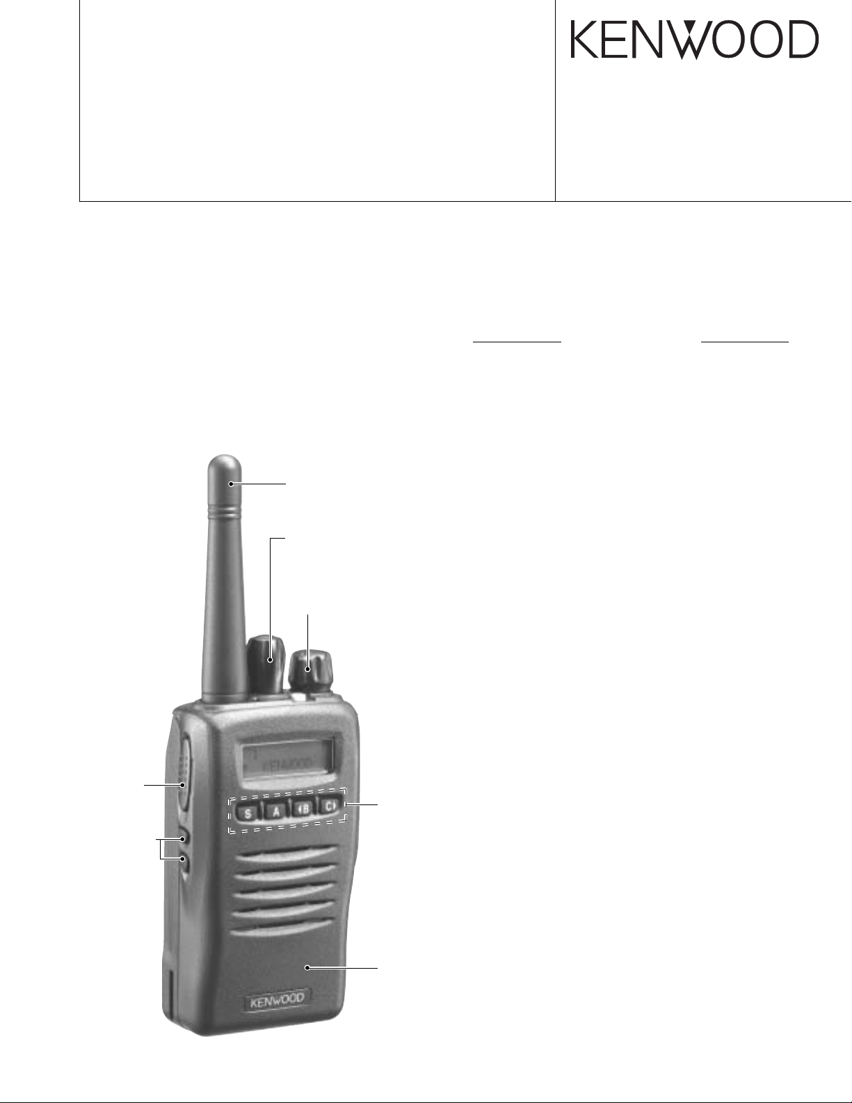
Knob (PTT)
(K29-9131-03)
Key top
(SW1,SW2)
(K29-9132-03)
Helical antenna
(T90-0798-05):E
(T90-0800-05):E3
Knob (ENC)
(K29-9134-03)
Knob (VOL)
(K29-9133-03)
© 2002-5 PRINTED IN JAPAN
B51-8631-00 (S) 582
CONTENTS
GENERAL ............................................................ 2
SYSTEM SET-UP ................................................ 2
OPERATING FEATURES .................................... 3
REALIGNMENT................................................. 13
CIRCUIT DESCRIPTION .................................... 17
SEMICONDUCTOR DATA ................................ 23
COMPONENTS DESCRIPTION ........................ 24
PARTS LIST....................................................... 25
EXPLODED VIEW.............................................. 34
PACKING ........................................................... 35
ADJUSTMENT .................................................. 36
TERMINAL FUNCTION..................................... 48
PC BOARD VIEWS
TX-RX UNIT (X57-6412-XX) (B/3),(C/3) ..... 49
TX-RX UNIT (X57-6412-XX) (A/3) .............. 53
SCHEMATIC DIAGRAM.................................... 59
BLOCK DIAGRAM............................................. 63
LEVEL DIAGRAM.............................................. 65
KSC-25,KNB-24L,KNB-25A,KNB-26N .............. 66
KBP-5,KMC-25................................................... 67
SPECIFICATIONS........................... BACK COVER
Packing
(4 keys)
(G53-1540-12)
Cabinet assy
(4 keys)
(A02-3653-14)
Page 2
TK-3140
GENERAL / SYSTEM SET-UP
INTRODUCTION
SCOPE OF THIS MANUAL
This manual is intended for use by experienced technicians
familiar with similar types of commercial grade
communications equipment. It contains all required service
information for the equipment and is current as of the
publication date. Changes which may occur after publication
are covered by either Service Bulletins or Manual Revisions.
These are issued as required.
PERSONNEL SAFETY
The following precautions are recommended for personnel
safety:
●
DO NOT transmit until all RF connectors are verified secure
and any open connectors are properly terminated.
●
SHUT OFF and DO NOT operate this equipment near
electrical blasting caps or in an explosive atmosphere.
●
This equipment should be serviced by a qualified technician only.
ORDERING REPLACEMENT PARTS
When ordering replacement parts or equipment information,
the full part identification number should be included. This
applies to all parts : components, kits, or chassis. If the part
number is not known, include the chassis or kit number of
which it is a part, and a sufficient description of the required
component for proper identification.
SYSTEM SET-UP
Merchandise received
Choose the type of transceiver
Transceiver programming
A personal computer (IBM PC or compatible), programming
interface (KPG-36), and programming software (KPG-74D (M2))
are required for programming.
(The frequency, conventional system features, TX power HI/LOW,
and signalling data are programmed for the transceiver.)
SERVICE
This radio is designed for easy servicing. Refer to the
schematic diagrams, printed circuit board views, and alignment
procedures contained within.
Frequency range (MHz) RF power Type
TX/RX 440~470
TX/RX 400~430
4.0W
4.0W
TK-3140 E
TK-3140 E3
Are you using the speaker microphone?
NO
Delivery
2
YES
KMC-25
Speaker microphone
(Option)
Page 3
OPERATING FEATURES
TK-3140
1. Operation Features
The TK-3140 is a UHF FM Radio designed in both 5tone
Model and DTMF/2tone/DMS Model. The programmable
features are summarized.
This transceiver can handle up to 250 groups with 250
channels in each group.
Model 5Tone Basic
Full
Full (Special Setting)
DTMF/2tone/DMS
1-1. 5tone Model
In this model, you can program Basic or Full level features.
When you select Basic level, only 1frame 5tone can be
programmed, and various functions are limited.
When you select “Special setting” in the Full Level, you
can use Encode/Decode format. Using Encode/Decode
format, you can further program the transceiver to run the
script.
1-2. DTMF/2tone/DMS Model
You can use Option signalling which is DTMF or 2tone(only
for Decode) or DMS(Digital Message System -FFSK
signalling) for every channel.
2 Rotary encoder
Rotate this encoder to activate its programmable function:
Channel Up/ Down (default) or Group Up/ Down. For further
details, contact your dealer.
3 POWER switch/ VOLUME control
Turn clockwise to switch ON the transceiver. Rotate to
adjust the volume. Turn counterclockwise fully to switch
OFF the transceiver.
4 LED indicator
This LED lights red during transmission and green while
receiving a signal. During Selective Call Alert, the LED
flashes orange. If programmed by your dealer, when the
battery pack power is low, the LED flashes red during
transmission. Replace or recharge the battery pack at this
time.
5 Auxiliary (orange) key
Press to activate its auxiliary function.
This key has no default setting.
6 Battery pack safety catch
Flip this catch to prevent accidentally pressing the battery
pack release latch.
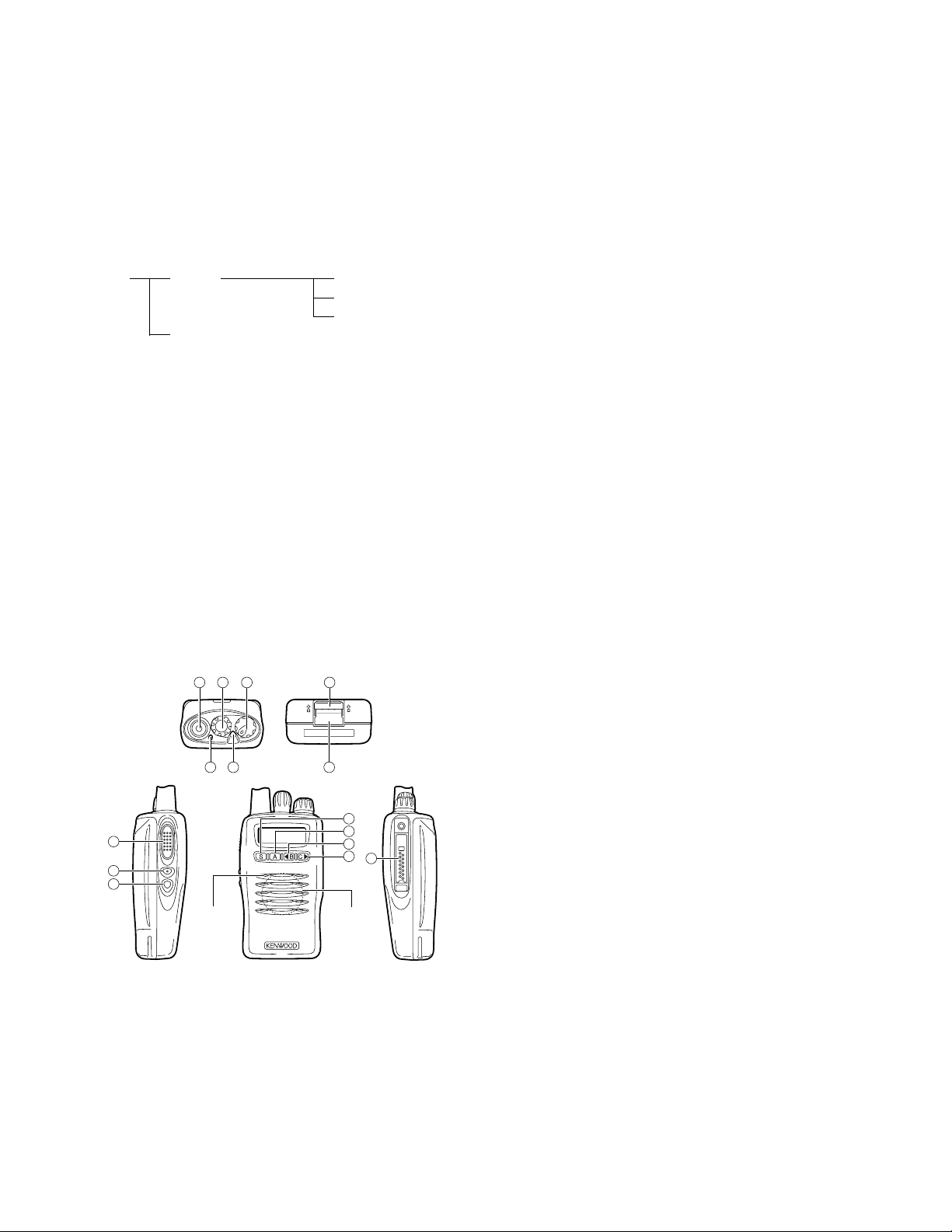
2. Transceiver Controls and Indicators
2-1. Physical Layout
16
8
9
10
Microphone Speaker
2-2. Panel controls
The key on the top and front panel is momentary-type push
buttons. The functions of these keys and knob are explained
below.
1 Antenna connector
Connect the antenna here.
32
4
57
11
12
13
14
15
7 Battery pack release latch
Press this latch to release the battery pack.
8 PTT (Push-To-Talk) switch
Press this switch, then speak into the microphone to call a
station.
9 Side 1 key
Press to activate its auxiliary function. The default setting
of this key is Monitor.
0 Side 2 key
Press to activate its auxiliary function. The default setting
of this key is Call 1 for the 5-Tone model. The DTMF/2Tone/DMS model has no default setting.
- S key
Press to activate its auxiliary function. The default setting
of this key is Selcall Entry for the 5-Tone model. The DTMF/
2-Tone/DMS model has no default setting.
= A key
Press to activate its auxiliary function. The default setting
of this key is Receive Entry for the 5-Tone model. The DTMF/
2-Tone/DMS model has no default setting.
3
Page 4
TK-3140
noitcnuF
/enoT-2/FMTD
ledoMSMD
ledoMenoT-5
tsiLsutatS+llacleSseYseY
tfihSseYseY
)zH0571(enoTelgniSseYseY
)zH5312(enoTelgniSseYseY
leveLhcleuqSseYseY
yratnemoMhcleuqSseYseY
ffOhcleuqSseYseY
yrtnEsutatSoNseY
tsiLsutatSoNseY
dnuorAklaTseYseY
OPERATING FEATURES
~ 2 B keys
Press to activate its auxiliary function. This key has no default
setting.
! C 3 keys
Press to activate its auxiliary function. This key has no default
setting.
@ Universal connector
Connect the (optional KMC-25) speaker/ microphone here.
Otherwise, keep the supplied cover in place.
2-3. Programmable keys
Keys 2, 5, and 9 to ! {pages 3 to 4} can be programmed
with the auxiliary functions listed in the following table. The
keys can only be programmed with functions, depending on
the model purchased. Please contact your dealer for further
details on these functions.
1
To access these functions, press and hold the appropriate
key for more than 1 second.
2
These functions can be programmed only on key 2, the
encoder.
3
This function can be programmed only on key 5, the
Auxiliary (orange) key, and on the programmable function
key of the optional KMC-25 speaker/ microphone.
noitcnuF
laiDotuAseYseY
1llaCoNseY
2llaCoNseY
3llaCoNseY
4llaCoNseY
5llaCoNseY
6llaCoNseY
nwoDlennahCseYseY
emaNlennahCseYseY
pUlennahCseYseY
3
llaCycnegremE
emuloVdexiFseYseY
nwoDpuorGseYseY
pUpuorGseYseY
2
nwoD/pUpuorG
lennahCemoHseYseY
kcoLyeKseYseY
pmaLseYseY
rewoPwoLseYseY
rotinoMseYseY
enoNseYseY
eueuQseYseY
4
nacSseYseY
drowssaPoidaRseYseY
yrtnEevieceRoNseY
ddA/eteleDnacSseYseY
yrtnEllacleSoNseY
tsiLllacleSseYseY
1
suounitnoCnwoDlennahC
1
suounitnoCpUlennahC
2
nwoD/pUlennahC
1
suounitnoCnwoDpuorG
1
suounitnoCpUpuorG
yratnemoMrotinoMseYseY
enoTelbatceleSrotarepOseYseY
seYseY
seYseY
seYseY
seYseY
seYseY
seYseY
seYseY
yrtnEsutatS+llacleSoNseY
/enoT-2/FMTD
ledoMSMD
ledoMenoT-5
■ Auto Dial
To transmit the stored DTMF code automatically.
Press the [Auto Dial] key to enter the “Auto Dial Mode”.
Select the desired number to send. It is used the selector
knob to select.
Press the [Auto Dial] key to transmit the numbers.
■ Channel Name
Press this key to switch between the “Channel Name” and
“Grp#/Ch#” for the display. If no channel name is programmed,
the transceiver automatically displays the group#/channel#.
■ Channel Up/Down
When this key is pressed each time, the channel number
to be selected is increased/decreased. If the “Hold” option
(Continuous Up/ Down operation) in the Key Assignment
window of the FPU is selected, press and hold the channel
Up or Down key for more than 1 second to repeat the operation
continuously. If you select the “Hold Delay” options in the
Key Assignment window of the FPU, the hold delay time can
be programmed. Although the default hold time is 3000 ms,
you can adjust the time between 100 and 5000 ms.
■ Call 1 to 6 (5tone)
Press the [CALL #] key to transmit the 5tone code that is
programmed to “Call #” in the System Parameters.
■ Emergency Call
Pressing this key causes the transceiver to enter the
emergency mode. The transceiver jumps to the programmed
“Emergency group/channel” and transmits for programmed
“Duration of Transmission time”.
The transceiver disables mic mute while transmitting. After
finishing transmission, the transceiver receivers for
programmed “Duration of Receiving”. The transceiver mutes
Page 5

OPERATING FEATURES
TK-3140
the speaker while receiving. Following the above sequence,
the transceiver continues to transmit and receive.
You can select whether or not the emergency ID is
transmitted in the emergency mode.
■ Fixed Volume
This function is used for changing the volume level, it is
Power on Tone, Control Tone, Warning Tone, Alert Tone, AF
Volume Type.
If these Tone is set up in “Fixed”, the Tone level can be
changed when [Fixed Volume] key is pressed.
When [Fixed Volume] key is pressed, Tone level changes
in turn to Low (Tone Volume Low), High (Tone Volume High)
and Off.
■ Group Up/Down
When this key is pressed each time, the group number to
be selected is increased/decreased. If the “Hold” option
(Continuous Up/ Down operation) in the Key Assignment
window of the FPU is selected, press and hold the Group Up
or Down key for more than 1 second to repeat the operation
continuously. If you select the “Hold Delay” options in the
Key Assignment window of the FPU, the hold delay time can
be programmed. Although the default hold time is 3000 ms,
you can adjust the time between 100 and 5000 ms.
■ Home Channel
Press this key once, the channel switches to the preprogrammed home channel.
■ Key Lock
Key Lock prevents accidental operation of the transceiver.
When Key Lock is activated, all keys other that PTT,
Emergency, Monitor, Monitor Momentary, Shift, Squelch,
Squelch Momentary, Lamp, Volume are locked.
“LOCKED” appears momentarily when the Key Lock key
is pressed.
■ Lamp
Press the [Lamp] key to toggle the display backlight ON or
OFF. The backlight automatically turns OFF approximately 5
seconds after it is switched ON.
Press any key other than [Lamp] while the backlight is ON
to reset the 5-second timer. The timer will reset and the
backlight will remain on for 5 seconds.
■ Low Power
When you press this key, “LO” appears and the transceiver
switches to RF Low Power.
If you press this key while “LO” is displayed, the Power
status reverts to the preset default setting. If “TX Power” is
set to ‘Low Power’, no change occurs.
■ Monitor
●
Model = DTMF/2tone/DMS:
When this key pressed once, “MON” icon lights and
squelch unmutes if a carrier is present, regardless of the
specified Signalling (including Option Signalling).
If pressed again, “MON” icon goes off and squelch mutes.
●
Model = 5tone:
Depend on Monitor Function and Monitor Key Action in
the System Parameters.
You can select either QT/DQT or 5tone decoding to be
canceled when Monitor key is pressed.
When Monitor function is activated, “MON” icon appears.
■ Monitor Momentary
●
Model = DTMF/2tone/DMS:
While pressing this key, “MON” appears and the squelch
unmutes if a carrier is present, regardless of the specified
Signalling (including Option Signalling).
If released, “MON” disappears, and the squelch mutes.
●
Model = 5tone:
Depend on Monitor Function in the System Parameters.
You can select either QT/DQT or 5tone decoding to be
canceled while pressing Monitor key.
When Monitor function is activated, “MON” icon appears.
■ Operator Selectable Tone
When this key is pressed, the “OST” appears and Encode/
Decode QT/DQT is switched to the OST Tone pair. If pressed
again, the “OST” display goes off and Encode/Decode QT/
DQT returns to transceivers pre-set.
When this key is held down for 1 sec, the transceiver enters
“OST Select Mode”. In this mode, the display shows OST No.
or OST Name which is set to the channel and operator can select
one of OST Tone pair using, the selector knob.
If pressed this key again, the displayed OST code is memorized
to the channel, the transceiver exits from the OST Select Mode,
returns to normal channel display and “OST” display.
38 kinds of OST Tone pairs can be programmed in the
Operator Selectable Tone window.
While in the OST Select mode, the transceiver does not
look back at the priority channel in the scan resume mode.
■ Queue
Press [Queue] key to toggle Queue mode ON or OFF.
When it is ON, you will see the contents of the Queue
buffer. You can scroll the Queue buffer using the selector
knob.
When you are in Queue mode, [C] key to toggle the Selcall
and Status displays.
When you are in Queue mode, press the [B] key to toggle
the Code and Selcall/Status displays.
Hold down the [C] key to delete the top stack of the Queue
buffer.
Hold down the [B] key to cancel Queue mode and return to
normal operation.
5
Page 6

TK-3140
OPERATING FEATURES
■ Radio Password
Back up is done even if the power supply is cut off.
A lock isn’t canceled unless a proper password is inputted.
The character which can be inputted is to 6 digits with the
number of 0 - 9. A lock is canceled if it is the same as Code
set up at “Optional Feature - Radio Password”.
If the entered Radio Password is incorrect, the “Key Input
Error Tone” sounds and the transceiver remains in “LOCK 1”
screen.
■ Receive Entry (5tone)
Press [Receive Entry] key to enter the desired Selcall code
you want to receive.
This function can be activated only when “RX Address” is
set to the channel and “Selectable Receive Digit” has been
entered.
When you enter Receive Entry mode, the “RX Address”
number appears on the LCD.
You use the channel selector to select the number. Then
press [B] key to enter the selected number. The selected digit
will shift left to enter the next digit.
Press [C] key to move the cursor 1 position right.
Hold down [C] key to clear the entered number.
■ Scan
Press the [Scan] key to toggle scanning the channels ON
and OFF. When the transceiver is scanning, “Revert CH
Display” is temporary disabled and the SCN icon and “-SCAN-”
appear.
■ Scan Delete/Add
Press the [Scan Del/Add] key to temporarily delete or add
each channel from/to the SCAN list.
When a channel is added to the SCAN list, (∞) appears on
LCD.
When the transceiver exits SCAN mode, the added or
deleted channels are erased from the SCAN list.
The original SCAN list is restored.
■ Selcall Entry (5tone)
Press [Selcall Entry] key to enter the desired Selcall code
you want to call.
This function can be activated only when “TX Address” is
set to the channel and “Selectable Selcall Digit” has been
entered. When you enter Selcall Entry mode, the “TX Address”
number appears on the LCD.
■ Selcall List
Press [Selcall List] key to enter Selcall List mode.
●
Model = 5tone:
Select the check box of “Selectable Selcall Digit”. The
number of digit you selected in “Selcall List” will be
displayed on LCD. If “Selcall List” has not been
programmed, same digits of Selcall List code that you
checked as “Selectable Selcall” digits will appear on LCD.
●
Model = DTMF/2tone/DMS:
The ID List code of DMS will appear on LCD.
To select the Selcall List, use the selector knob.
■ Selcall+Status Entry
Select the selcall number you wish to call.
Press [Selcall + Status Entry] key to enter “Selcall Entry
Mode”.
If you press [Selcall + Status Entry] key again, it works as
“Status Entry Mode”.
■ Selcall+Status List
Select the selcall number you wish to call.
Press [Selcall + Status List] key to enter “Selcall List Select Mode”.
If you press [Selcall + Status List] key again, it works as
“Status List Select Mode”.
■ Single Tone (1750Hz)/Single Tone (2135Hz)
While [Single Tone (1750Hz)] key is pressed and held, the
1750Hz tone is transmitted.
While [Single Tone (2135Hz)] key is pressed and held, the
2135Hz tone is transmitted.
■ Shift
It allows you to enable [Shift + Function] key access. When
[Shift] key is pressed, SFT appears on LCD.
■ Squelch Level
Press [Squelch Level] key to enter “Squelch Level
Adjustment Mode”.
The squelch level can be adjusted by the selector knob.
Press [Squelch Level] key again to store the adjusted
squelch level.
■ Squelch Momentary
Press [Squelch Momentary] key to force the squelch
unmute. “MON” icon appears on LCD and BUSY LED (Green)
lights.
If released, the squelch unmutes and “MON” disappears.
Also, BUSY LED (Green) goes off.
■ Squelch Off
Press [Squelch Off] key to force the squelch unmute.
“MON” icon appears on LCD and BUSY LED (Green) lights. If
the key is pressed again, the squelch unmutes and “MON”
disappears. Also, BUSY LED (Green) goes off.
■ Status Entry (5tone)
It allows the operator to input the status and transmit it to
the base station.
Both TX Address and “Selectable Status Digit” must be
programmed to perform the operation.
Press [Status Entry] key to access Status Entry mode.
“TX Address” of the channel appears on LCD.
6
Page 7
OPERATING FEATURES
TK-3140
Selector knob to select the desired number and press [B]
key to enter. The cursor moves to next position.
■ Status List (5tone)
Press [Status List] key to enter Status List mode.
Select the check box of “5tone - System Parameters Selectable Status Digit”. The number of digit you selected in
“5tone - Status List” will be displayed on LCD. If “Status List”
has not been programmed, same digits of Status List code that
you checked as “Selectable Status” digits will appear on LCD.
To select the Status List, use the selector knob.
■ Talk Around
When Talk Around function is activated, “TA” appears and
the transceiver transmits on the receive frequency, using
receiver’s QT/DQT code.
The operator can call the other party directly (without
repeater).
■ None
When you press this key, the transceiver emits the “Key
Input Error Tone” (no function is performed).
2-4. Display
3. Scan Operating
1) Scan types
●
Single Group Scan
You can scan all valid (ADD) channels in the displayed group
that can be selected with the group selector.
●
Multiple Group Scan
You can scan all valid (ADD) channels in the all valid (ADD)
group.
2) Scan Start Condition
One or more non-priority channels must be added to all
channels that can be scanned. The transceiver must be in
normal receive mode (PTT off).
When you activate the key programmed to the scan
function, the scan starts. The scan icon “SCN” lights and
“-SCAN-” or revert channel (programmable) is indicated on
alphanumeric display.
3) Scan Stop Condition
The scan stops temporarily if the following conditions are
satisfied.
1 A carrier is detected, then signalling matches on channels
for which receive the signalling is set by the programming
software.
2 A carrier is detected on the channel for which receiving
signalling is not set by the programming software or when
the monitor (signalling cancel) function is activated.
rotacidnI noitpircseD
.desserp
woL .desserpsi
.egassem
(▼ eratahtslennahcswohsrotacidniddaehT.)
:etoN afoecalpniseirettabenilaklagnisunehW
4) Scan Channel Types
1 Priority channel is the most important channel for the scan,
and always detects a signal during scan and when the scan
.sgnitteselbammargorprelaedsuoirav
sallewsarebmunlennahcdnapuorgehtsyalpsiD
.detcelessilennahCytiroirPehtnehwsraeppA
sademmargorpyekehtnehwsraeppA rotinoM si
.reviecsnartsihtnodesutonsinocisihT
.nacSgnimrofrepnehwsraeppA
sademmargorpyekehtnehwsraeppA rewoPFR
.reviecsnartsihtnodesutonsinocisihT
eueuqehtniderotssiegassemanehwsraeppA
wenaevieceruoynehwsehsalF.yromem
)emanro(rebmunlennahcdnapuorgehtsyalpsiD
S or 5tone.MDgnisunehwsegassemdeviecerdna
rotacidniddanasadesusitnemgestsomtfelehT
thgirehT.ecneuqesgninnacsehtfotuodekcolton
otro)(llaCevitceleSrofdesusitnemgestsom
rewopyrettabfoleveletamixorppaehtyalpsid
llufmorfsegnarrotacidniyrettabehT.gniniamer
.spets4ni)(ytpmeot)(
ylreporptonyamrotacidniyrettabeht,kcapyrettab
.gniniamerrewopyrettabehtetacidni
stops temporarily.
2 Non-priority channels detects a signal during scan. For the
channels that can be selected with the group or channel
selector when the scan does not occur, adds an indicator
(∞) lights.
5) Priority Channel Setting
A priority channel can be set as follows with the
programming software (KPG-74D (M2)).
1 Specify a priority channel as a fixed priority channel.
2 Make a selected channel a priority channel.
6) Scan Type According to the Priority Channel
1 When no priority channel is set : Only the non-priority
channels are scanned.
If a non-priority channel stops temporarily, it stops until
there is nosignal on the channel.
2 When priority channel is set : Either priority channel is
scanned.
If a non-priority channel stops temporarily, a priority channel
signal is detected at certain intervals.
If a priority channel stops temporarily, it stops until there
is no signal on the priority channel.
7
Page 8

TK-3140
OPERATING FEATURES
7) Revert Channel
The revert channel is used to transmit during scanning and
set by the programming software (KPG-74D (M2)).
1 Priority
The transceiver reverts to the priority channel.
2 Priority with talkback
The transceiver reverts to the priority channel.
If you press PTT during a resume timer (dropout delay time,
TX dwell time) or calling, you can transmit on current
channel to answer to the call however revert channel is
set to priority channel.
After resume time, scan re-starts and transmission channel
is return to priority channel.
3 Selected channel
The transceiver reverts to the channel before scanning or
the channel that you changed during scan.
4 Last called channel
The transceiver reverts to the last called channel during
the scan.
5 Last used channel
The transceiver reverts to the last used (transmitted)
channel during scan. “Last used” revert channel includes
talkback function.
6 Selected with talkback
The transceiver reverts to the channel before scanning or
the channel that you changed during scan.
8) Scan End
When you reactivate the key programmed to the scan
function during scan mode, the scan ends.
The scan icon “SCN” and “-SCAN-” or revert channel
(programmable) display goes off.
9) Temporarily Delete/Add
It is possible to delete or add channel temporarily during
scan. When scan stops on unnecessary channel for example
by interference of the other party, activate the delete/add
function (for example press the key), then that channel is
deleted temporarily and scan re-start immediately.
When you would like to add the deleted channel temporarily
to scan sequence, select the desired (deleted) channel during
scan, activate the delete/add function (for example press the
key) before scan re-start.
That channel is added temporarily to scan sequence. The
temporary deleted or added channels are returns to pre-set
delete/add, when the transceiver exits from scan mode.
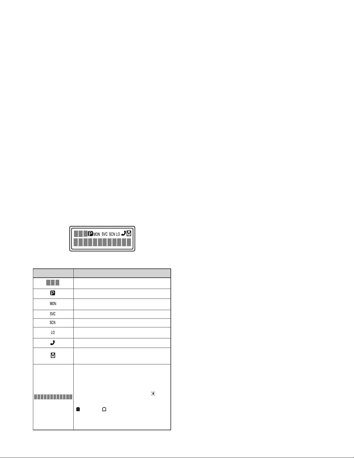
2) Sub LCD display
You can use 3-digit the display to display the channel number
or group number. It is useful when the main (12-digit) display
indicates, group or channel name or other functions.
3) Selective Call Alert LED
You can select whether or not the LED on the transceiver
flashes in an orange color when selective call was occurred.
4) PTT ID
PTT ID provides a DTMF or FFSK (DMS : Fleet-ID) ANI to
be sent with every time PTT (beginning of transmission, end
of transmission, or both).
You can program PTT ID “on” or “off” for each channel.
The contents of ID are programmed for each transceiver.
The timing that the transceiver sends ID is programmable.
BOT : DTMF ID (BOT)/FFSK ID is sent on beginning of
transmission.
EOT : DTMF ID (EOT)/FFSK ID is sent on end of
transmission.
Both : DTMF ID (BOT)/FFSK ID is sent on beginning of
transmission and DTMF ID (EOT)/FFSK ID is sent on end of
transmission.
5) Radio password
When the password is set in the transceiver, user can not
use the transceiver unless enter the correct password.
This code can be up to 6 digits from 0 to 9 and input with
the selector knob, and [Side 2] key.
6) Minimum Volume
The minimum volume is programmable (off (0) to 31). The
transceiver remains the minimum volume level however the
mechanical volume position is set to zero.
7) “TOT” Pre-Alert
The transceiver has “TOT” pre-alert timer. This parameter
selects the time at which the transceiver generates “TOT”
pre-alert tone before “TOT” is expired.
“TOT” will be expired when the selected time passes from
a TOT pre-alert tone.
8) “TOT” Re-Key Time
The transceiver has “TOT” re-key timer. This timer is the
time you can not transmit after “TOT” exceeded. After “TOT”
re-key time expired you can transmit again.
4. Details of Features
1) Time-out timer
The time-out timer can be programmed off or in 1 second
increments from 30 seconds to five minutes. If the transmitter
is keyed continuously for longer than the programmed time,
the transmitter is disabled and a warning tone sounds while
the PTT button is held down. The alert tone stops when the
PTT button is released.
8
9) “TOT” Reset Time
The transceiver has “TOT” reset timer. This timer is the
minimum wait time allowed during a transmission that will
reset the “TOT” count.
“TOT” reset time causes the “TOT” to continue even after
PTT is released unless the “TOT” reset timer has expired.
Page 9

OPERATING FEATURES
TK-3140
10) OST (Operator Selectable Tone)
The transceiver is capable to have “OST” function and 38
tone pair (QT/DQT) with max 10-digit name for each tone pair.
• “OST” Back Up
The transceiver is programmable the selected “OST” code
is memorized or not. If you set to Disable (no memorized), the
“OST” function always starts at “off”.
• Selectable No Tone
“TONE OFF” can be selected in the OST Select mode when
you select the “Selectable No Tone” option in the Operator
Selectable Tone window. When it is unchecked, the TONE
OFF setting is ignored.
11) Clear to Transpond
The transceiver waits the transpond of 5tone/2tone/DTMF
if channel is busy until channel open. This feature prevents
the interference to other party.
12) Battery Warning/Status
The battery warning function checks the battery voltage
level automatically. If the battery voltage drops to a
predetermined value, the operator will be notified.
The Battery Status function shows the current remaining
battery capacity in 4 different levels (High, Sufficient, Low and
Very low).
Unless the Battery Warning/Status function is set to OFF,
the low battery warning function is activated when the
transceiver detects the low battery voltage. The transceiver
either beeps, the “Lo” icon blinks, the red LED blinks or the
Very Low indicator (Battery) blinks, depending on the
transceiver’s settings.
Then more low voltage is detected during transmission,
the transceiver does not transmit and the warning tone beeps
while the PTT key is pressed.
Measurements given by this function should be used just
as a reference.
15) Com Port
This function selects the external serial port function at the
universal connector (TXD/RXD). PC programming is accepted,
regardless of this setting.
5. Option Signalling (DTMF/2tone)
Built-in DTMF decoder is available for option signalling.
Built-in 2-Tone decoder is available for option signalling.
It is possible to use individual call, group call, stun, kill. Stun
and kill are used with DTMF only.
Preset operation is triggered when matches with Option
Signaling
When Option Signaling matches on a Group Channel where
set to Yes, the Option Signaling display flashes and Option
Signaling is canceled. Settings after this will cause
“Transpond” or “Alert” to sound.
Setting the Selective Call Alert LED will make an orange
LED start flashing.
Mute or Unmute is triggered by the ID/QT/DQT/Carrier when
option signaling is a match (when Option Signal is deactivated
by a transmission).
AND/OR
Option Signaling match conditions can be selected with
AND/OR logic.
Alert/Transpond AF Mute Open
AND
match with DTMF.
by receiving the carrier.
Triggers at match with QT/ Triggers at match with QT/
DQT/ID+DTMF (2tone);Both
OR
Triggers only for match with
DTMF (2tone) : Opt QT/DQT/ID;Signaling
Even if set for OR, AF mute cannot be canceled just by a
In channels not set with QT/DQT, signaling is a match just
DQT/ID+DTMF (2tone);
Triggers only for match with
Both
13) Battery Save
Battery Saver becomes active when the squelch is closed.
The receiver circuit power is toggled ON and OFF to prolong
battery life, except in Scan mode.
The “ON” time is automatically selected by the signal
conditions.
The “OFF” time is selectable as [OFF], [Short](200ms),
[Med](400ms) and [Long](800ms).
14) Auto Light on
You can use the transceiver to turn on the backlight
automatically when a key is pressed.
You can turn off the back light by pressing the [Lamp] key
while the backlight is ON. You can manually turn on the light
at any time by pressing the [Lamp] key.
Auto Reset
When Option Signaling matches on a Group channel where
set to Yes, Option Signaling is canceled when it matches a
group channel set to Yes.
After Option Signaling is a match, Option Signaling can
automatically set to Reset after a specified time.
Stun/Kill
If the Stun code matches, a predetermined action will occur.
Whether option signalling is activated or not, when stun code
matches on any channel, the transceiver will become stun or kill.
While stun is active (“LOCK 2” appears), if the stun code +
“#” code is received, stun will disactive.
While kill is active (“ERROR” appears), the transceiver will
be disable all functions. The transceiver must be
reprogrammed by the FPU (KPG-74D (M2)) to operation again.
9
Page 10

TK-3140
OPERATING FEATURES
6. Alphanumeric Two-way Paging Function
(Digital Message System)
■ General
The Alphanumeric Two-way Paging Function (DMS) is a
Kenwood proprietary protocol. It enables a variety of paging
functions.
■ ID Construction
A radio unit ID is defined by a combination of 3-digit Fleet
and 4-digit ID numbers. Each radio unit must be assigned its
own Fleet and ID numbers.
■ Digital Message System [DMS]
●
Inter-fleet Call
Configure the transceiver to respond calls from stations that
have a different fleet number.
■ PTT ID
A pre-programmed unique ID can be sent at the beginning
of transmission and/or the end of transmission to identify which
radio unit is on air.
■ Selective Call (SELCALL)
This is a voice call to a particular individual or group of stations.
●
Example of call types;
[100][ALL ] : <Group Call>
All the units whose fleet number is “100” are called.
[100][1000] : <Individual Call>
The unit, whose the fleet number is “100” and ID number
is “1000”, is called.
[ALL][ALL ] : <Broadcast Call>
All the units are called.
[ALL][1000] : <Supervisor Call>
All ID “1000” are called regardless of their fleet number.
●
Unit ID Encode Block
This function limits the usable IDs using the Block function.
If Inter-fleet Call is enabled, block ID setting affects each
fleet group.
■ Status Message
Using a 2-digit number, you can send and receive a Status
message which may be decided in your talk group. Each Status
may be displayed with 16 alphanumeric characters if
programmed in the radio. A maximum of 15 received messages
can be stored in the stack memory, and it can be reviewed
after reception. If the message memory becomes full, the
oldest one will be erased. The stack memory will be cleared
by turning radio power off.
●
Automatic Status Response
If you pre-select a status number and leave the radio in the
Status Mode, it can automatically respond with the selected
status number upon request from the base station. (The
request function is initiated by serial control on the base
station (Optional).)
■ Short Message (Optional)
A maximum of 48 characters can be sent (External
equipment is required). Received Short Messages will be
displayed in the same manner as a Status Message. A
maximum of 15 received messages can be stored in the stack
memory. In the Stack Mode, 3-digit LCD indicates the received
Short Message as “Q1”~”Q15”.
■ Long Message
A maximum of 4096 characters can be sent (External
equipment is required). Received Long Message will not be
displayed or stacked in the radio memory but is output through
the COM (Data) port.
■ Emergency Function
Emergency status 99 will be sent at the beginning of each
emergency transmission.
●
Emergency Status response
“Alert” can be selected for the called radio unit’s response
to reception of status 99 which is used as an emergency
status.
■ Other Functions
●
Data TX with QT/DQT
Whether programmed QT/DQT is modulated or not with a
data transmission except for Selcall. A radio unit can receive
a data message regardless of QT/DQT if the receiving unit
is not scanning.
●
DMS Baud Rate
FFSK data baud rate setting. The same rate must be set as
a communication partner.
1200bps :
Data communication is made in 1200bps. The
communication area is much wider than 2400bps.
Recommended for repeater operation.
2400bps :
Data communication is made in 2400bps. The
communication area is narrower than 1200bps, but it will
decrease the data traffic. Data rate 2400bps may not work
properly depending on the repeater’s characteristic.
●
Inter-fleet call
●
Status/Short/Long Message on Data Group/Channel
Status/Short/Long Message transmission is made whether
on the Data Group/Channel.
10
Page 11

OPERATING FEATURES
●
Status/Short/Unit ID Message Serial Output
Whether a received Status/Short message or PTT ID is
outputed or not to serial port.
■ Parameters
●
GTC Count
Number of “Go To data Channel” messages to be sent
before transmitting a data message if it is being made on
Data Group/Channel. If a radio unit receives a GTC message,
it will move to the Data Group/Channel of the current Group.
Increase this item to make sure the called radio unit moves
to the Data Group/Channel.
●
Random Access (Contention)
When a channel is busy, radio unit will not transmit
(depending on its Busy Channel Lockout setting). As soon
as a channel is cleared, some transmissions may crash.
Random access is used to avoid this by employing a random
transmission sequence.
TK-3140
7. 5tone
When you select 5tone Model, you can set the following
options.
When you select Basic level features, only 1 frame 5tone
format can be programmed.
When you select Full level features, up to 3 frame 5tone
format can be programmed.
Enabling “Setting Level” on each menu, you can also use
“Encode/decode format”.
Using “Encode/decode format”, you can further program
the transceiver to run the script.
■ 5tone Standard
The selected 5tone Standard is used for 5tone encoding
and decoding.
Range:
ZVEI, CCIR, EEA, PZVEI, DZVEI, PCCIR, PDZVEI, ZVEI-2,
EIA, Natel, AP-369, Kenwood
●
Number of Retries
Number of Retries is the maximum number of retry
transmission when no acknowledgement is received in the
Maximum ACK Wait Time. Increase this item to improve
data communication reliability.
●
TX Busy Wait Time
TX Busy Wait Time is the maximum amount of time before
giving up the data transmission when the channel is busy.
Also, this timer affects if it expires during Random Access
period.
●
Maximum ACK Wait Time
Maximum ACK Wait Time is the maximum amount of time
to wait for an acknowledgement from the called radio unit.
It is used as an interval time of retries. It must be set greater
than the ACK Delay Time of the called radio unit.
●
ACK Delay Time
ACK Delay Time is the amount of time from the end of
receiving a data to the beginning of sending an
acknowledgement. It should be adjusted as the repeater’s
hang-up delay time. Also, it must be set less than the
Maximum ACK Wait Time of the calling radio unit.
●
TX Delay Time (RX Capture)
TX Delay Time is the amount of unmodulated transmission to
let the called unit stop scanning or exit its battery save mode.
It is used only when starting a data communication sequence.
●
Data TX Modulation Delay Time
Data TX Modulation Delay Time is the amount of time from
the beginning of transmission to the beginning of a data
modulation. It is used every time data is transmitted.
■ Monitor Function
You can select either QT/DQT or 5tone decoding to be
canceled when [Monitor] or [Monitor Momentary] key is
pressed.
When Monitor function is activated, “MON” icon appears.
When the transceiver is set up in “QT/DQT, cancels the
decoding in QT/DQT Decode.
The squelch is controlled by the signal carrier only.
When the transceiver is set up in “5tone”, cancels the
decoding in 5tone Decode.
The squelch is controlled by QT/DQT Decode only.
If QT/DQT code is programmed in QT/DQT Decode, incoming
signal must match the QT/DQT code to open the squelch.
■ Busy Channel Lockout
You can inhibit the transmission while the channel is busy.
You can program the following different conditions.
When the transceiver is set up in “Lockout 1”:
Do not transmit when the transceiver is receiving the carrier.
Transmit when the transceiver is not receiving the carrier.
When the transceiver is set up in “Lockout 2”:
Do not transmit when the transceiver is receiving the carrier
and QT/DQT code does not match.
Transmit when the transceiver is not receiving the carrier
or receiving the QT/DQT code matches.
■ Selectable Receive Digit
Select the check box to change Receive Code (maximum 8
digits) manually when receiving Decode Code. You cannot
select Selectable Receive Digit, Store Selcall Digit and Store
Status Digit at the same time.
For example, the transceiver receives 5tone code, #59401
when you have 4th and 5th digit checked in Selectable Receive
Digit menu. In this case, #01 is stored as Receive Code.
Press [Receive Entry] key to enter Receive Entry mode.
11
Page 12

TK-3140
OPERATING FEATURES
When you enter Receive Entry Mode, you can change the
Receive Code, #01.
You can receive the Receive Code after the modification.
■ Selectable Selcall Digit
Select the check box to change Selcall Code (maximum 8
digits) manually when transmitting Encode Code. You cannot
select Selectable Selcall Digit and Selectable Status Digit at
the same time.
For example, the transceiver receives 5tone code, #59401
when you have 4th and 5th digit checked in Selectable Selcall
Digit menu. In this case, #01 is stored as Selcall.
Press [Selcall Entry] key to enter Selcall Entry mode.
When you enter Selcall Entry Mode, you can change the
Selcall Code, #01.
You can transmit the Selcall after the modification.
■ Selectable Status Digit
Select the check box to change Status Code (maximum 8
digits) manually when transmitting Encode Code. You cannot
select Selectable Selcall Digit and Selectable Status Digit at
the same time.
For example, the transceiver receives 5tone code,
#5940167 when you have 6th and 7th digit checked in
Selectable Status Digit menu.
Press [Selcall Entry] key to enter Status Entry mode.
When you enter Status Entry Mode, you can change the
Status Code, #67.
You can transmit the Status code after the modification.
■ Automatic Close
It compares the selected digits of RX Address code in
Channel menu when the transceiver receives 5tone signalling.
If the selected digits matches to the received 5tone code, the
transceiver closes Monitor. You can select maximum 8 digits
of RX Address.
■ Copy from TX/RX Address
You can select to copy the digit to the memory when you
change the channel, using the selector knob.
Receive Digit in “RX Address” is copied when the channel
is changed. Selcall/Status Digit in “TX Address” is copied when
the channel is changed.
■ Encode Code
When “Special Setting” is disabled, you can select the
Encode Code to transmit when [Call 1-6] key is pressed.
You can select up to 3 codes to transmit 3-frame 5tone
code. The Encode Code is transmitted from left to right digit.
24 different Encode Codes are available.
When “Special Setting” is enabled, you can select the
Encode Format setting from #1 to #32.
You can select the Encode Format name, configured in
Encode Format menu.
12
■ Decode Code
When “Special Setting” is disabled, you can select the
Decode Code setting from #1 to #8.
The transceiver tries to decode the selected Decode Code
setting (maximum 8 different settings) at the same time. When
the code matches in “5tone Code” menu, the transceiver
operates as programmed in “Decode Code” menu.
When “Special Setting” is enabled, you can select the
Decode Format setting from #1 to #32.
You can select the Decode Format name, configured in
Decode Format menu.
You can program the 5-tone code you want to receive for
each channel. At the same time, you can be on stand-by for a
Single tone.
If the 5-tone code set in your transceiver matches a received
code, Monitor is activated and a beep sounds. You can display
the received 5-tone code on the LCD screen and transmit an
acknowledgement to the Base station. Furthermore, you can
activate the stun and kill features.
■ Selcall/Status List
You can program Selcall or Status Message when you select
the party from the List to make a 5tone selective call. Or you
want to display Selcall(Status) Code or Message when you
receive the call.
Maximum 8-digit can be programmed for the Code and 100
different Selcalls or Status are available for Selcall/Status List.
You can assign 16 alphanumeric characters to each
message.
■ Programmable Alert Tone
You can program the alert type from type 1 to type 8, when
the expected 5-tone is received.
You can program the number of times to repeat outputting
and frequency and duration for the Alert Tone.
When you select “Special Setting”, you can further
configure the beep tone type from No. 1 to No. 47, using the
Encode/Decode format.
■ Encode/Decode Format
You can use Encode/Decode Format script function when
you select “Feature Level”=FULL and “Special Setting”
=Enabled.
In order to write the Encode/Decode Format script, you
need the technical knowledge of 5tone signalling functions.
Of course, you can write the script to perform all the functions
that you can do with “Feature Level”=BASIC and FULL and
“Special Setting”=Disabled. (Menu driven method)
In addition, you can write the original script to control various
functions and signalling timing.
Refer to each function of Encode/Decode Format Code for
details. Sample scripts are also available in the KPG-74D (M2).
You can create 32 different types of Encode/Decode
Formats. You can assign a name up to 12 characters for each
Encode/Decode Format.
Page 13
OPERATING FEATURES / REALIGNMENT
TK-3140
8. Audible User Feedback Tones
The transceiver outputs various combinations of tones to
notify the user of the transceiver operating state. The main
tones are listed below.
■ Power on tone
This tone is output when the transceiver is turned on. (The
high tone is output for 500ms.)
■ Alert tone
This tone is output when the transceiver is TX inhibition for
TOT, battery warning and PLL unlocked. It is output until the
PTT button is released.
■ Group call tone
Sounds when a group call with the correct DTMF/2-tone
option signalling is received.
■ DMS signalling alert tone
Sounds when an individual call with the correct DMS
signalling is received.
■ Individual call tone
Sounds when an individual call with the correct DTMF/2tone option signalling is received.
■ Key press tone [A]
Sounds when a key is pressed. For toggle keys, sounds
when toggle function is turned on (key press tone [B] sounds
when it is turned off).
■ Key press tone [B]
Sounds when a key is pressed. For toggle keys, sounds
when the toggle function is turned off (key press tone [A]
sounds when it is turned on).
■ Key press tone [C]
Sounds when a key is pressed. Also sounds when storing
data, adding a DTMF code to memory, and when changing
test mode settings.
■ Key input error tone
Sounds when a key is pressed but that key cannot be used.
■ Roll over tone
Sounds at the smallest group/channel.
■ Transpond tone
Sounds when an individual call with the correct DTMF/2tone option signalling is received. For group calls, only the
group tone will sound, not the transpond tone.
REALIGNMENT
1. Modes
User mode
Panel test mode
PC mode
Firmware
programming mode
Clone mode
Self programming
mode
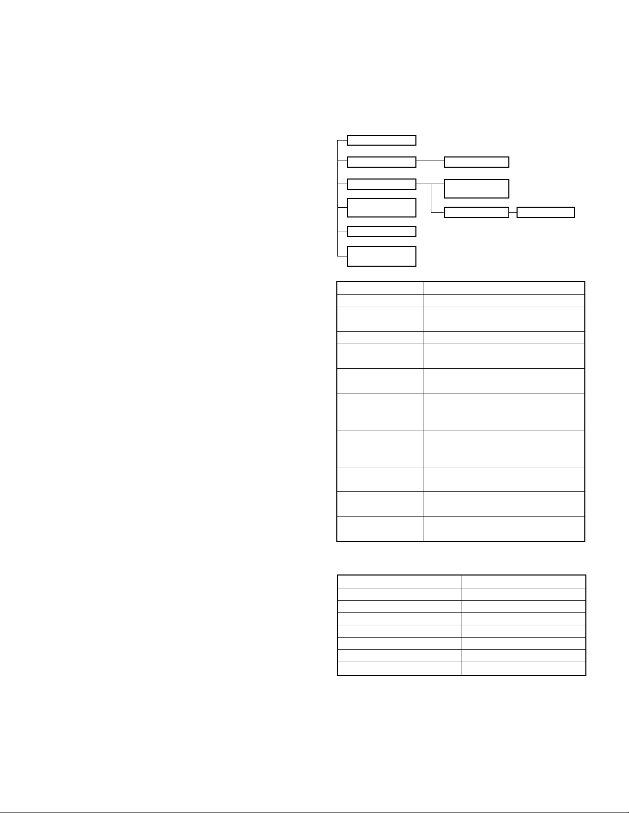
Mode Function
User mode For normal use.
Panel test mode Used by the dealer to check the
Panel tuning mode Used by the dealer to tune the radio.
PC mode Used for communication between the
Data program- Used to read and write frequency data
ming mode
PC test mode Used to check the radio using the PC.
PC tuning mode Used to check the radio using the PC.
Firmware program- Used when changing the main
ming mode program of the flash memory.
Clone mode Used to transfer programming data
Self programming Frequency, signalling and features
mode write to the radio.
Panel tuning mode
Data programming
mode
PC test mode
fundamental characteristics.
radio and PC (IBM compatible).
and other features to and from the radio.
This feature is included in the FPU.
See panel test.
This feature is included in the FPU.
See panel tuning.
from one radio to another.
PC tuning mode
2. How to Enter Each Mode
Mode Operation
User mode Power ON
Panel test mode [A]+Power ON
PC mode Received commands from PC
Panel tuning mode [Panel test mode]+[S]
Firmware programming mode
Clone mode [C]+Power ON
Self programming mode [Side 2]+Power ON
[S]+Power ON
3. Panel Test Mode
Setting method refer to ADJUSTMENT.
■ Pre alert tone
Sounds prior to the TOT TX inhibit activation. If TOT pre
alert is set, the tone sounds at the amount of time
programmed, before the TOT expires (TOT time–TOT pre alert
time = Pre alert tone sounding time).
4. Panel Tuning Mode
Setting method refer to ADJUSTMENT.
13
Page 14
TK-3140
REALIGNMENT
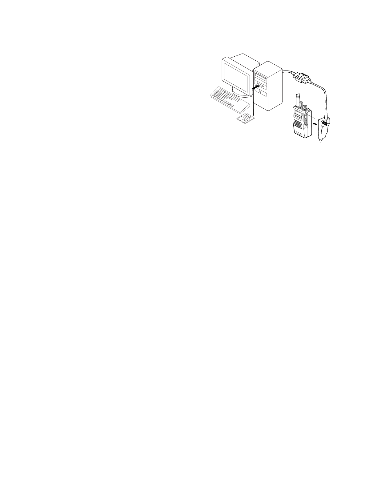
5. PC Mode
5-1. Preface
The TK-3140 transceiver is programmed by using a personal
computer, programming interface (KPG-36) and programming
software (KPG-74D (M2)).
The programming software can be used with an IBM PC or
compatible. Figure 1 shows the setup of an IBM PC for
programming.
5-2. Connection procedure
1. Connect the TK-3140 to the personal computer with the
interface cable.
2. When the POWER switch on, user mode can be entered
immediately. When PC sends command the radio enter
PC mode, and “PROGRAM” is displayed on the LCD.
When data transmitting from transceiver, the red LED is
blinking.
When data receiving to transceiver, the green LED is blinking.
Notes:
• The data stored in the personal computer must match
model type, when it is written into the flash memory.
• Change the TK-3140 to PC mode, then attach the interface
cable.
5-3. KPG-36 description
(PC programming interface cable: Option)
The KPG-36 is required to interface the TK-3140 to the
computer. It has a circuit in its D-subconnector (25-pin) case
that converts the RS-232C logic level to the TTL level.
The KPG-36 connects the universal connector of the TK3140 to the computers RS-232C serial port.
5-4. Programming software KPG-74D (M2) Description
The KPG-74D (M2) is the programming software for the
transceiver supplied on three 3.5” floppy disks. This software
runs under MS-Windows 95/98/Me/2000 on an IBM-PC or
compatible machine.
The data can be input to or read from the trnsceiver and
edited on the screen. The programmed or edited data can be
printed out. It is also possible to tune the transceiver.
We recommend that install the KPG-74D (M2) for example
to hard disk first then use it.
5-5. Programming with IBM PC
If data is transferred to the transceiver from an IBM PC
with the KPG-74D (M2), the destination data (basic radio
information) for each set can be modified. Normally, it is not
necessary to modify the destination data because their values
are determined automatically when the frequency range
(frequency type) is set.
The values should be modified only if necessary. Data can
be programmed into the flash memory in RS-232C format via
the universal connector.
14
IBM-PC
KPG-36
KPG-74D (M2)
Fig. 1
6. Firmware Programming Mode
6-1. Preface
Flash memory is mounted on the TK-3140. This allows the
TK-3140 to be upgraded when new features are released in
the future. (For details on how to obtain the firmware, contact
Customer Service.)
6-2. Connection procedure
Connect the TK-3140 to the personal computer (IBM PC or
compatible) with the interface cable (KPG-36). (Connection is
the same as in the PC Mode.)
6-3. Programming
1. Start up the firmware programming software (Fpro.exe).
2. Set the communications speed (normally, 57600 bps) and
communications port in the configuration item.
3. Set the firmware to be updated by File name item.
4. Turn the TK-3140 power ON with the [S] switch held down.
Hold the switch down until the display changes to “PROG
57600”. When “PROG 57600” appears, release your finger
from the switch.
5. Check the connection between the TK-3140 and the
personal computer, and make sure that the TK-3140 is in
the Program mode.
6. Press write button in the window. A window opens on the
display to indicate progress of writing. When the TK-3140
starts to receive data. the [P] icon is blinking.
7. If writing ends successfully. the LED on the TK-3140 lights
and the checksum is displayed.
8. If you want to continue programming other TK-3140s,
repeat steps 4 to 7.
Notes:
●
This mode cannot be entered if the Firmware Programming
mode is set to Disable in the Programming software (KPG74D (M2)).
●
When programming the firmware, it is recommend to copy
the data from the floppy disk to your hard disk before update
the radio firmware.
Directry copying from the floppy disk to the radio may not
work because the access speed is too slow.
Page 15
REALIGNMENT
TK-3140
6-4. Function
1. If you press the [Side 1] switch (top of left side) while
“PROG 57600” is displayed, the version is displayed. If
you press the [Side 1] switch again while the version is
displayed, “PROG 57600” is redisplayed.
2. If you press the [Side 2] switch (bottom of left side) while
“PROG 57600” is displayed, the display changes to “PROG
19200” to indicate that the write speed is low speed (19200
bps). If you press the [Side 2] switch again while “PROG
19200” is displayed, the display changes to “PROG 38400”,
and the write speed becomes the middle-speed mode
(38400 bps). If you press the [Side 2] switch again while
“PROG 38400” is displayed, the display returns to “PROG
57600”.
3. If you press the [Side 2] switch while the version is
displayed, the checksum is displayed. If you press the [Side
2] switch again while the checksum is displayed, the version
is redisplayed.
Note:
Normally, write in the high-speed mode.
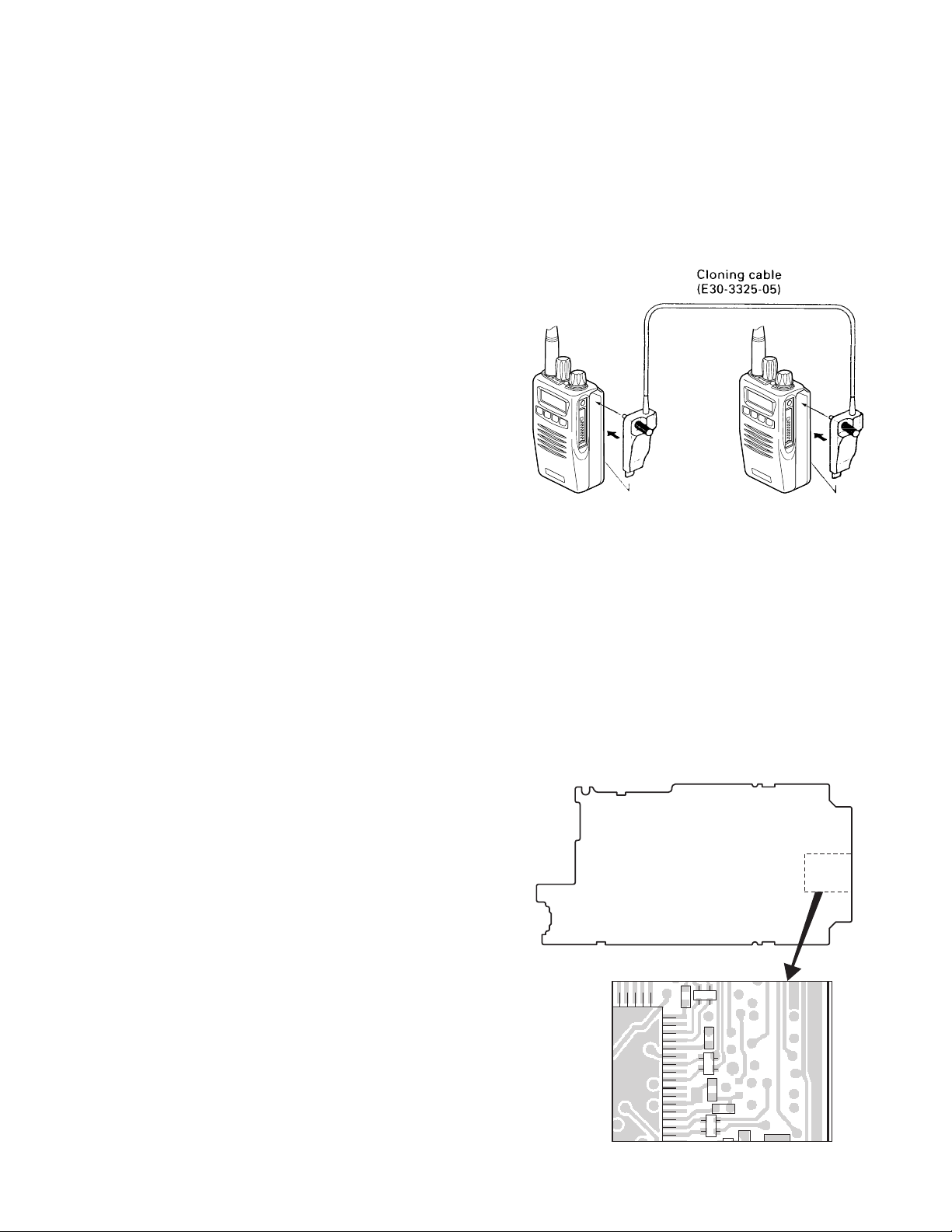
7. Clone Mode
Programming data can be transferred from one radio to
another by connecting them via their external universal
connectors. The operation is as follows (the transmit radio is
the master and the receive radio is a slave).
1. Turn the master TK-3140 power ON with the [C] key held
down. If the Data password is set to the TK-3140, the TK3140 displays “CLONE LOCK”. If the password is not set,
the TK-3140 displays “CLONE MODE”.
2. When you enter the correct password, and “CLONE
MODE” is displayed, the TK-3140 can be used as the
cloning master. The following describes how to enter the
password.
3. How to enter the password with the encoder;
If the encoder is rotated while “CLONE LOCK” is displayed,
numbers (0 to 9) are displayed flashing. When you press
the [C] key, the currently selected number is determined.
If you press the [Side 2] key after entering the password in
this procedure, “CLONE MODE” is displayed if the entered
password is correct. If the password is incorrect, “CLONE
LOCK” is redisplayed.
4. Power on the slave TK-3140.
5. Connect the cloning cable (No. E30-3325-05) to the
universal connectors on the master and slave.
6. Press the [C] key on the master while the master displays
“CLONE MODE”. The data of the master is sent to the
slave. While the slave is receiving the data, “PROGRAM”
is displayed. When cloning of data is completed, the master
displays “END”, and the slave automatically operates in
the User mode. The slave can then be operated by the
same program as the master.
7. The other slave can be continuously cloned. When the [C]
key on the master is pressed while the master displays
“END”, the master displays “CLONE MODE”. Carry out
the operation in step 4 to 6.
Note:
Only the same models can be cloned together.
Fig. 2
8. Self Programming Mode
Write mode for frequency data and signalling etc. Mainly
used by the person maintaining the user equipment.
8-1. Enter to the self programming mode
Delete R351 (Figure 3) in the TX-RX unit and turn the power
switch on while pressing the [Side 2] key. When enter the
self programming mode, “SELF PROG” is displayed.
Note :
This mode (self programming mode) cannot be set when it
has been disabled with the FPU.
TX-RX UNIT (A/3)
Component side
51
50
IC309
R351
Fig. 3
15
Page 16
TK-3140
REALIGNMENT
8-2. Channel Setting Mode
This is a mode for making channel settings with the panel
keys without using the FPU.
Pressing [Side 1] when [SELF PROG] is displayed, sets
Channel Setting Mode.
Select an item set with [C] and change the selection with
the encoder.
The data displayed with [B] is stored in the memory and
then proceeds to the next item. Pressing [C] proceeds to
the next item without storing it in the memory.
Press [Side 1] to set the display to [SELF PROG] and return
to reset (default) status.
●
Flow Chart
Self programming mode
[Side 1]
[Side 1]
[Side 1]
[Side 1]
[Side 1]
[Side 1]
[Side 1]
[Side 1]
[Side 1]
[Side 1]
[Side 1]
16
Channel setting mode
[B]
RX frequency
[B]/[C]
RX signalling
[B]/[C]
TX frequency
[B]/[C]
TX signalling
[B]/[C]
Scan delete/add
[B]/[C]
RF Power High/Low
[B]/[C]
Beat shift yes/no
[B]/[C]
Wide 5k/Wide 4k/Narrow
[B]/[C]
Compander
[B]/[C]
[Side 2]
[Side 2]
[Side 2]
[Side 2]
Items set in Channel Setting Mode are as follows.
Function settings
Channel select
Display Remarks
Channnel
or Group
RX Frequency RXF [Side 2] : Freq. On/Off switching
RX Signalling RXS [Side 2] : OFF/QT/DQT switching
TX Frequency TXF Key operation same as RX
TX Signalling TXS Key operation same as RX
Scan Delete/Add
SCN DEL/ADD
RF Power PWR HIGH/LOW
Beat Shift SFT YES/NO
Wide 5k/Wide 4k
w/s/n Wide 5k/Wide 4k/Narrow
/Narrow
Compander CMP ON/OFF
Channel selection Group selection
OFF
OFF QT
[Side 2]
OFF
OFF
[Side 2]
[C]
QT
[Side 2]
DQT N
[Side 2]
[Side 2]
DQT N
[Side 2]
8-3. Memory Reset Mode
This mode is used to clear data for functions that can be
set in Self Programming Mode or to return to reset values
(default).
Pressing [S] when [SELF PROG] is shown, sets the display
to [CLEAR NO?].
Turning the encoder alternately switches the display
between [CLEAR NO?] [CLEAR YES?].
Pressing [S] when [CLEAR YES?] is shown, clears the data
and sets the display to [ALL CLEAR].
Pressing [S] again, returns the display to [SELF PROG].
Pressing [S] when [CLEAR NO?] is shown, returns the
display to [SELF PROG] without resetting the data.
[A] : 5kHz/6.25kHz/1MHz step
switching
[A] : 1 step/Standard switching
[S] : DQT Normal/Invert swtiching
Frequencies
Signalling
DQT I
[S]
DQT I
[S]
Page 17
CIRCUIT DESCRIPTION
TK-3140
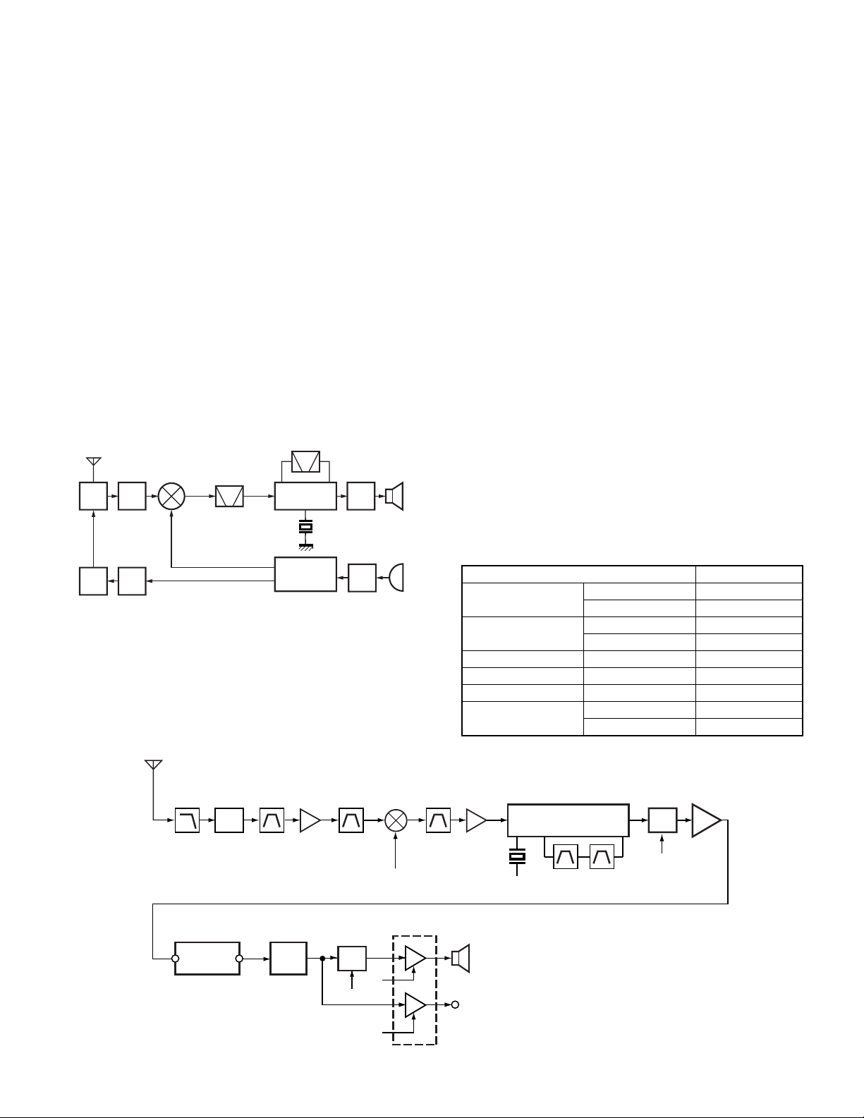
1. Overview
This transceiver is UHF/FM portable transceiver designed
to operate in the frequency range of 440 to 470MHz (E) and
400 to 430MHz (E3).
2. Circuit Configuration by Frequency
The receiver is a double-conversion superheterodyne with
a first intermediate frequency (IF) of 44.85MHz and a second
IF of 455kHz. Incoming signals from the antenna are mixed
with the local signal from the PLL to produce the first IF of
44.85MHz.
This is then mixed with the 44.395MHz second local
oscillator output to produce the 455kHz second IF. This is
detected to give the demodulated signal.
The transmit signal frequency is generated by the PLL VCO,
and modulated by the signal from the microphone. It is then
amplified and sent to the antenna.
TX/RX : 440~470MHz : E
400~430MHz : E3
ANT
1st MIX
SW
PA
RF
AMP
TX
AMP
395.15~425.15MHz : E
355.15~385.15MHz : E3
440~470MHz : E
400~430MHz : E3
ANT
AMP
MCF
44.85MHz
CF
455kHz
FM IF
SYSTEM
PLL
VCO
AMP
44.395MHz
MIC
AMP
AF
SP
MIC
Fig. 1 Frequency configuration
3. Receiver System
3-1. RF unit
An incoming RF signal from the antenna terminal is passed
through the antenna switch (D102, D103, D104. and D105
are off) and then the bandpass filter (L215,217). High pass
ANT
filter HPF (L219) the 1st image response improve. And the
bandpass filter is adjusted by a variable capacitor. The input
voltage to the variable capacitor is regulated by the voltage
output from the D/A converter (IC307). The signal is amplified
by RF amplifier Q207, and passed through the bandpass filter
(L209,210,211). The resulting signal is applied to the first mixer
(Q206), where it is mixed with the first local oscillator signal
output from the frequency synthesizer to produce the first IF
(44.85MHz).
3-2. IF unit
The first IF signal is passed through a four-pole monolithic
crystal filter (XF200) to remove a adjacent channel signal. The
filtered first IF signal is amplified by the first IF amplifier (Q205)
and then applied to the lF system IC (IC200). The IF system IC
provides a second mixer, second local oscillator, limiting
amplifier, quadrature detector and RSSI (Received Signal
Strength Indicator). The second mixer mixes the first IF signal
with the 44.395MHz of second local oscillator output (crystal
unit X200) and produces the second IF signal of 455kHz.
The second IF signal is passed through the ceramic filter
(CF200 : Wide, CF201 : Narrow) to more remove the adjacent
channel signal. The filtered second IF signal is amplified by
the limiting amplifier and demodulated by the quadrature
detector with ceramic discriminator (CD200). The demodulated
signal is routed to the audio circuit.
Center Frequency Nominal 455kHz
Band Width
Stop Band Attenuation
3dB Min. ±6.5kHz
50dB Max. ±15.5kHz
±18~±33kHz Min. 55.0dB
±100kHz Min. 50.0dB
Spurious Response 0.1~1.0MHz Min. 20.0dB
Ripple Within 455±6.5kHz Max. 2.0dB
Insertion Loss at 455 kHz Max. 4.0dB
Group Delay Time
Within 455±3.0kHz Max. 25.0µ sec
Within 455±5.0kHz Max. 50.0µ sec
Table 1 Ceramic filter (L72-0995-05): CF200
L110,111
L112
ANT
SW
D102,103
D104,105
IC501
23 20
AUDIO IC
L215,217
BPF
IC307
VOL
Q207
RF
AMP
L209,210
L211
Q308
SSW
BPF
SW
VC1
VC2
Q206
1st MIX
1st Local
OSC (PLL)
IC313
AF PA
XF200
MCF
Fig. 2 Receiver section
Q205
IF AMP
X200
INT.
SP
EXT.
SP
2nd local
OSC
IC200
MIX, DET, IF
CF200
CF201
: Wide
: Narrow
Q204
SW
DMDM
IC303 (1/2)
AF AMP
17
Page 18
TK-3140
CIRCUIT DESCRIPTION
Center Frequency Nominal 455kHz
Band Width
Stop Band Attenuation
6dB Min. ±4.5kHz
40dB Max. ±10.0kHz
±100kHz Min. 25.0dB
Ripple Within 455±3.0kHz Max. 1.5dB
Insertion Loss at 455 kHz Max. 6.0dB
Table 2 Ceramic filter (L72-0996-05): CF201
3-3. Wide/Narrow switching circuit
Wide and Narrow settings can be made for each channel
by switching the ceramic filters CF200 (Wide), CF201 (Narrow).
The WIDE (high level) and NARROW (low level) data is
output from IC311.
Regardless of NARROW or WIDE band selection, signals
always pass through the filter, CF200.
When the WIDE band is selected, Q201 is turned ON, then
D202 and D203 are turned OFF.
So, the signal does not pass through the filter CF201. When
the NARROW band is selected, Q201 is turned OFF, then D202
and D203 are turned ON. So, the signal passes through the
filters, CF200 and CF201.
Q202 turns on/off with the Wide/Narrow data and the IC200
detector output level is changed to maintain a constant output
level during wide or narrow signals.
3-4. Audio amplifier circuit
The demodulated signal from IC200 goes through the mute
switch (Q204) and is amplified by IC303 (1/2), high-pass filtered,
low-pass filtered, high-pass filtered, and de-emphasized by
IC501.
The signal then goes through an electronic volume control
(IC307), and an AF switch (Q308 is on), and is routed to audio
power amplifier (IC313), where it is amplified and output to
the internal speaker.
The audio mute signal (AM1) from the shift register
becomes Low in the standby and Q302, Q303 which are power
supply circuit for IC313 turn off. Also, IC501 is set to the power
down mode according to data from microprocessor, and the
AF signal is muted. When the audio is output, AM1 becomes
High to turn Q302, Q303 ON, and voltage is supplied to power
terminal VP of IC313. Also, IC501 is canceled out of the power
down mode.
The speaker is switched by the logic of speaker switching
terminal SSW on the universal connector. When SP-MIC is
not attached, the logic of SSW becomes High and SW (Q308)
is turned ON, and the AF signal is input to both amplifiers of
IC313.
When SP-MIC is attached, SSW is connected to GND at
inside of SP-MIC. For this reason, Q308 is turned OFF, and
the AF signal is input only to amplifier for EXT SP of IC313.
Change of INT/EXT SP refer to Fig. 4.
5R
IC200
MIXOUT
C221
IFIN
CF200
R255
R221
CD200
QUAD
IFOUT
AFOUT
Q201
D202 D203
R208
AFOUT
R210
R264
R256
CF201
R211
C206
R222
R213
Q202
5CNS
C210
R216
W/N
(IC311 pin14)
AM1 SSW VC1 VC2 SP
HH HLINT
HL LHEXT
LH LLMUTE
LL LLMUTE
AM1
SSW
SB
AF
Q305
Q302
Q308
SW
Q307
Q303
VC1
2
VC2
8
Fig. 4 Audio amplifier circuit
VP 5
INT.SP
EXT.SP
IC313
18
Fig. 3 Wide/Narrow switching circuit
Page 19

CIRCUIT DESCRIPTION
TK-3140
3-5. Squelch circuit
The output from IC200 goes to Wide/Narrow noise level
selector (Block A in Fig. 5) and enters to FM IC again. The
noise level selector is able to change amount of Wide and
Narrow noise component by Q903. When the Wide band is
selected, Q903 is turned ON, the noise pass through R916,
R917, TH902. When the Narrow band is selected, Q903 is
turned OFF, the noise pass through R914, R915, TH901. The
noise component passed through 2 band-pass filter one in
IC200 and IC201 (2/2). The output from IC201 (2/2) is amplified
by Q208 and rectified by D201 to produce a DC voltage
corresponding to the noise level. The DC voltage is sent to
the analog port of the CPU (IC309). And IC200 outputs a DC
voltage (RSSI) corresponding to the input of the IF amplifier.
The CPU reads the RSSI signal via pin 93.
IC309 determines whether to output sounds from the
speaker by comparing the input voltage of pin 91 and pin 93
with the preset value.
5R
R911R918
Q903
R915
R913
D902 D903
R914 TH901
R916
R912
TH902
R917
R919
R920
91
IC309
CPU
IF AMP
W/N
IC200 : FM IF IC
DET
A
R212
R910
C275
C207
The signal from microphone is amplified by IC502 and
limited by AGC circuit composed of D500, D501, Q502 and
Q504. IC501 on the small board is composed of high-pass
filter, low-pass filter and pre-emphasis/IDC circuit.
The signal passes through the D/A converter (IC307) for
the maximum deviation adjustment, and enters the summing
amplifier consisting of IC305 (1/2), and is mixed with the low
speed data from the CPU (IC309).
The output signal from the summing amplifier passes
through the D/A converter (IC307) again and goes to the VCO
modulation input.
The other output signal from the summing amplifier passes
through the D/A converter (IC307) again for the BAL
adjustment, and the buffer amplifier (IC302 2/2), and goes to
the TCXO modulation input.
EXT.
MIC
MIC
Q301
SW
Q305
MSW
MIC
IC502 IC501
3
AMP
AGC
D500,D501
Q502,Q504
AUDIO IC
7
D/A
IC305 (1/2)
LSD
OUT
SUM
AMP
IC307
I5 O5 I2 O2
IC307
IC307 IC302(2/2)
I1 O1
D/A
D/A
BUFF
AMP
VCO
Fig. 7 Microphone amplifier
X1
TCXO
C909
IC201
(2/2)
Q208
RSSI
BPF
BPF
AMP
AMP
12
7
NOISE
AMP
D201
DET
93
Fig. 5 Squelch circuit
SQ voltage
SQ close
SQ open
ANT inpot level
Preset
value
RSSI voltage
Preset value
ANT inpot level
Fig. 6 Squelch and RSSI voltage vs ANT input level
4. Transmitter System
4-1. Microphone amplifier
The signal from the internal microphone goes through the
mute switch (Q301).
When the SP-MIC is not attached, the microphone
switching terminal (MSW) on the universal connector becomes
High, and mute switch (Q301) is turned ON. When the SPMIC is attached, MSW is connected to GND at inside of SPMIC. For this reason, Q301 is turned OFF, the internal
microphone is muted, and only the input of the external
microphone is supplied to the microphone amplifier.
4-2. Drive and Final amplifier
The signal from the T/R switch (D101 is on) is amplified by
the pre-drive (Q100 and 101) drive amplifier (Q103) to
+15~17dBm.
The output of the drive amplifier is amplified by the RF
power amplifier (Q106) to 4.0W (1W when the power is low).
The RF power amplifier is MOS FET transistor. The output of
the RF power amplifier is then passed through the harmonic
filter (LPF) and antenna switch (D102,103 are on) and applied
to the antenna terminal.
From
T/R SW
(D101)
Q100
Pre-DRIVE
AMP
+B
REF
VOL
(IC307)
Q101 Q103 Q106
Pre-DRIVE
AMP
R119
R120
R123
DRIVE
AMP
IC100
(1/2)
RF
POWER AMP
VDD
IC100
(2/2)
VGG
D102,103
ANT
SW
Fig. 8 Drive and final amplifier and APC circuit
4-3. APC circuit
The APC circuit always monitors the current flowing through
the drive amplifier (Q103) and the RF power amplifier (Q106)
and keeps a constant current. The voltage drop at R119, R120
and R123 is caused by the current flowing through the RF
power amplifier and this voltage is applied to the differential
amplifier (IC100 1/2).
ANT
LPF
19
Page 20

TK-3140
CIRCUIT DESCRIPTION
IC100(2/2) compares the output voltage of IC100(1/2) with
the reference voltage from IC307, and the output of IC100(2/
2) controls the VGG of the RF power amplifier to make the
both voltages to same voltage.
The change of power high/low is carried out by the change
of the reference voltage. Q105,107 and 108 are turned on in
transmit and the APC circuit is active.
5. Frequency Synthesizer Unit
5-1. Frequency synthesizer
The frequency synthesizer consists of the TCXO (X1), VCO,
PLL IC(IC801) and buffer amplifiers.
The TCXO generates 16.8MHz. The frequency stability is
2.5ppm within the temperature range of –30 to +60˚C. The
frequency tuning and modulation of the TCXO are done to
apply a voltage to pin 1 of the TCXO. The output of the TCXO
is applied to pin 1 of the PLL IC.
The TK-3140’s VCO consists of 2VCO and covers a dual
range of the 395.15~425.15MHz, the 440~470MHz (E),
355.15~385.15MHz, 400~430MHz (E3). The VCO generates
395.15~425.15MHz (E), 355.15~385.15MHz (E3) for providing
to the first local signal in receive. The operating frequency is
generated by Q3 in transmit mode and Q2 in receive mode.
The oscillator frequency is controlled by applying the VCO
control voltage, obtained from the phase comparator (IC801)
to the variable capacitor diodes (D1 and D3 in transmit mode
and D2 and D4 in receive mode).
The T/R pin of IC312 goes “high” in receive mode causing
Q4, Q6 and Q3 to turn off, and Q2 turn on. The T/R pin goes
“low” in transmit mode.
The outputs from Q2 and Q3 are amplified by buffer
amplifier (Q5) come to the amplifiers.
The PLL IC consists of a prescaler, reference divider, phase
comparator, charge pump (The frequency step of the PLL
circuit is 5 or 6.25kHz). The input signal from the pins 1 and 10
of the PLL IC is divided down to the 5 or 6.25kHz and compared
at phase comparator. The pulsed output signal of the phase
comparator is applied to the charge pump and transformed
into DC signal in the loop filter (LPF). The DC signal is applied
to the CV of the VCO and locked to keep the VCO frequency
constant.
PLL data is output from DP (pin 73), CP (pin 74) and EP (pin
72) of the microprocessor (IC309). The data are input to the
PLL IC when the channel is changed or when transmission is
changed to reception and vice versa. A PLL lock condition is
always monitored by the pin 30 (UL) of the microprocessor.
When the PLL is unlocked, the UL goes low.
T/R
(TX : Low)
LPF
UL
CPU
IC309
T/R
VCO
DP,CP,EP
CV
IC801
PLL
8
Q8
BUFF
Q803
BUFF
To mixer
106
1
MB
TCXO
X1
SW
IC302
D101
SW
D100
FC
BAL
To
drive
amp
Fig. 9 PLL block diagram
6. Control Circuit
The control circuit consists of microprocessor (IC309) and
its peripheral circuits. It controls the TX-RX unit and transfers
data to and from the LCD ASSY. IC309 mainly performs the
following;
1) Switching between transmission and reception by PTT
signal input.
2) Reading system, group, frequency, and program data
from the memory circuit.
3) Sending frequency program data to the PLL.
4) Controlling squelch on/off by the DC voltage from the
squelch circuit.
5) Controlling the audio mute circuit by decode data input.
6) Transmitting tone and encode data.
6-1. Memory circuit
Memory circuit consists of the CPU (IC309) and a flash
memory (IC308). A flash memory has a capacity of 2M bits
and contains the transceiver control program for the CPU. It
also stores the data for transceiver channels and operating
parameter that are written by the FPU. This program can be
easily written from an external devices.
The EEPROM (IC310) stores the last channel data, the scan
on status, and other parameters.
●
Flash Memory
Note : The flash memory stores the data that is written by the
FPU (KPG-74D (M2)), and firmware program (User mode, Test
mode, Tuning mode, etc.). This data must be rewritten when
replacing the flash memory.
●
EEPROM
Note : The EEPROM stores tuning data (Deviation, Squelch,
etc.).
Realign the transceiver after replacing the EEPROM.
IC309
CPU
IC310
EEPROM
20
FLASH
IC308
Fig. 10 Memory circuit
Page 21

CIRCUIT DESCRIPTION
TK-3140
6-2. Low battery warning
The battery voltage is monitored by the microprocessor
(IC309 pin90 : BATT1). When the battery voltage falls below
the voltage set by the Low Battery Warning adjustment during
the transmission, the red LED blinks to notify the operator
that it is time to replace the battery (When the “On TX” option
(default setting) under the Battery Warning / status function
in the FPU is selected.). If the battery voltage falls even more
(NiCd, NiMH, Alkaline : approx. 5.8V, Li-ion: approx. 6.1V),
the transceiver does not transmit and the warning tone beeps
while the PTT switch is pressed.
Low battery warning
The red LED blinks during
the transmission.
The red LED blinks and
the warning tone beeps while
the PTT switch is pressed.
Battery condition
The battery voltage is low but
the transceiver is still usable.
The battery voltage is low and
the transceiver is not usable
to make calls.
6-3. Battery type detection
The transceiver automatically detects the battery type,
measuring the resistance between the S-terminal and +
terminal on the battery pack and changes the supplied voltage
to the S-terminal as below. The microprocessor then detects
the battery type.
Resistor value Battery type
1.8MΩ Li-ion 0.3~1.3V
560kΩ Ni-Cd 1.3~2.6V
220kΩ Ni-MH 2.6~5.0V
OPEN Battery case 0~0.3V
Input voltage of S-terminal
7. Signalling Circuit
7-1. Encode
●
Low-speed data (QT,DQT)
Low-speed data is output from pin 1 of the CPU. The signal
passes through a low-pass CR filter, and goes to the summing
amplifier (IC305 1/2). The signal is mixed with the audio signal
and goes to the VCO and TCXO (X1) modulation input after
passing through the D/A converter (IC307) for BAL adjustment.
●
High-speed data (5 tone, DTMF)
High-speed data (HSD) is output from pin 2 of the CPU.
The signal passes through a low-pass filter consisting of IC304,
and provides a TX HSD tone and a RX HSD tone. TX HSD
deviation making an adjustment by microprocessor is passed
through the D/A convertor (IC307), and then applied to the
audio processor (IC501).
The signal is mixed with the audio signal and goes to the
VCO and TCXO, the RX HSD tone is passed a summing
amplifier (IC305 1/2), the D/A converter (IC307) for audio
control, audio power amplifier and then to the speaker.
●
FFSK
FFSK signal is output from pin 7 of IC501. The signal passes
through the D/A converter (IC307) for the FFSK deviation
adjustment. and is routed to the VCO. When encoding FFSK,
the microphone input signal is muted.
LSD
OUT
1
IC309
CPU
HSD
OUT
I6
IC304 (1/2)
2
LPF
SUM
IC305 (1/2)
I3
O5
I2
I1
D/A (ADJ)
IC307
O6
AF AMP
O3
I5
O2
IC302 (2/2)
O1
BUFF
AMP
RX Audio
SUM
SUM
MIC IN
MD
MB
IC501
VCO
X1
TCXO
Fig. 13 Encode
21
Page 22

TK-3140
Q404
5RC
5TC
5R
5T
5CNS
IC402
CE
IC403
CE
IC401
IC404
Q405
RF power amp (Q103 and Q106)
+B
F400
SB
D405
ON/OFF
VOL
5C
14
VCC
RESET
INT
10
71
R740
IC400
IC309
CPU
R403
C425
CIRCUIT DESCRIPTION
7-2. Decode
●
Low-speed data (QT,DQT)
The demodulated signal from the IF IC (IC200) is amplified
by IC303 (1/2) and passes through a low-pass filter (IC306) to
remove audio components. The signal is input to pin 95 of the
CPU.
The CPU digitizes this signal, performs processing such as
DC restoration, and decodes the signal.
●
High-speed data (DTMF)
The DTMF input signal from the IF IC (IC200) is amplified
by IC303 (1/2) and goes to IC500, the DTMF decoder. The
decoded information is then processed by the CPU. During
transmission and standby, the DTMF IC is set to the power
down mode when the PD terminal is High. When the line is
busy, the PD terminal becomes Low, the power down mode
is canceled and decoding is carried out.
●
High-speed data (2 tone, 5 tone)
The demodulated signal from the IF IC (IC200) is amplified
by IC303 (1/2) and passes through an audio processor (IC501)
and amplifier IC201 (1/2) and comparator IC305 (2/2) to remove
a low-speed data. The CPU digitizes this signal, performs
processing such as DC restoration, and decodes the signal.
8. Power Supply Circuit
Battery +B is supplied via a 3A fuse from the battery terminal
connected to the TX-RX unit. After passing through the power
switch, power supply (SB) is applied to the three AVRs. IC401
supplies 5V (5M) to the control circuit, and IC403 supplies 5V
(5C) to common circuits. IC402 supplies to the TX circuit, the
RX circuit and common circuits of needless save mode. During
transmission, 5TC becomes Low and Q405 is turned ON to
supply 5V (5T) to the TX circuit. During reception, 5RC becomes
Low and Q404 is turned ON to supply 5V (5R) to the RX Circuit.
The power supply voltage monitor IC (IC404) monitors
power supply voltage (SB). If the voltage falls (less than 5V),
the VOUT port goes “LOW” level, the CPU INT port also goes
“LOW” level, and the CPU stops.
●
FFSK
The FFSK input signal from the IF IC is amplified by IC303
(1/ 2) and goes to pin 23 of IC501. The signal is demodulated
by FFSK demodulator in IC501. The demodulated data goes
to the CPU for processing.
COMPARATOR
95
11
IC305
LSD
IN
IC311
IC309
CPU
IC303
AMP
X501
3.58MHz
IC501
AF IC
IC306
LPF
IC500
DTMF
DECODE
OSCI
PD
DCK,SD,STD
Fig. 14 Decode
IC201
AMP
3
HSD
IN
Fig. 15 Power supply circuit
DT,CK,CE
22
Page 23

SEMICONDUCTOR DATA
Microprocesser : 30620M8A-2W6GP (TX-RX UNIT : IC309)
■ Pin function
Pin Port
No. Name
1 LSDO O Low speed data output.
2
HSDO
3 HSDI I High speed data input.
4
DSTB
5NC - NC
6 BYTE - +5V.
7 CNVSS - GND.
8 AFRDT I/O MODEM FFSK decode data input.
9 AFDAT O MODEM FFSK encode data output.
10 RESET - CPU reset.
11 XOUT - CPU clock.
12 VSS - GND.
13 XIN - CPU clock.
14 VCC - +5V
15 NC - NC
16 DTSTD I DTMF decoder data detect input.
17 AFTRD I MODEM FFSK encode data output timing
18 AFRTM I MODEM FFSK decode data Input timing
19 EEPDAT I/O EEPROM data input/output.
20 BEEP O Beep output.
21 SKEY I [S] Key input.
22 AKEY I [A] Key input.
23 BKEY I [B] Key input.
24 CKEY I [C] Key input.
25 AUX I [AUX] Key input.
26 PTT I [PTT] Key input.
27 SIDE2 I [Side 2] Key input.
28 SIDE1 I [Side 1] Key input.
29 SSW I Speaker Mic detect input.
30 UL I PLL unlock detect input.
31
DTMDAT
32 DTCLK O DTMF decoder clock output.
33 TXD O Serial interface (COM0) TXD0 (to MIC
34 RXD I Serial interface (COM0) RXD0 (to MIC
35 DAT O Common data output.
36 CLK O Common clock output.
37 RDY - Can not used.
38 ALE - Can not used.
39 HOLD - Can not used.
40 HLDA - Can not used.
41 BLCK - Can not used.
42 RD O Flash memory RD bus.
43 BHE - Can not used.
44 WR O Flash memory WR bus.
45 SAVE O Battery save output.
46 SELF I Self programming mode enable input.
47
CS/MODE
48 CSO O Flash memory chip enable.
49 A19 - Can not used.
I/O Function
O High speed data output.
O D/A converter data strobe output.
MODEM serial input/output.
pulse input.
pulse input.
I DTMF decoder data input.
connector).
connector).
O LCD driver chip select output.
Pin Port
No. Name
50~59
A18~A9 O Flash memory address bus.
60 VCC - +5V
61 A8 O Flash memory address bus.
62 VSS - GND.
63~70
A7~A0 O Flash memory address bus.
71 INT I Low voltage detection
72 EP O PLL IC Data Strobe output.
73 DP O PLL IC Data output.
74 CP O PLL IC Clock output.
75~78
EN4~1 I Rotary SW input 4~1.
79~86
D7~D0 I Flash memory data bus.
87 PF I SP-Mic PF switch input.
88 VOL I Volume level input.
89 BATT2 I Battery distinction input.
90 BATT1 I Battery voltage
91 ASQL I Squelch level input.
92 TEMP I Thermistor input.
93 RSSI I Received signal strength indicator input
94 AVSS - GND.
95 LSDI I Low speed data input.
96 VREF - +5V
97 AVCC - +5V
98 SFTSTB O Shift register data strobe output.
99 OE O Shift register output enable output.
100 AFDIR O MODEM DIR.
TK-3140
I/O Function
(RSSI).
23
Page 24

TK-3140
TX-RX UNIT (X57-6412-XX)
Ref. No.
IC100 MOS IC APC AMP
IC200 MOS IC IF IC
IC201 MOS IC AF AMP Filter
IC302 MOS IC AF AMP Filter
IC303 MOS IC AF AMP Filter
IC304 MOS IC AF AMP Filter
IC305 MOS IC AF AMP Filter
IC306 MOS IC AF AMP Filter
IC307 MOS IC Potential Meter
IC308 ROM IC Flash ROM
IC309 MPU MPU
IC310 ROM IC EEPROM
IC311,312 MOS IC Shift Register
IC313
IC400 MOS IC Detector
IC401 MOS IC 5M AVR
IC402 MOS IC 5CNS AVR
IC403 MOS IC 5C AVR
IC404 MOS IC Detector
IC500 MOS IC DTMF Decoder
IC501 MOS IC Base Band IC
IC502 MOS IC AF AMP, AGC
IC801 MOS IC PLL IC
IC901 MOS IC 5TC Buffer
Q100
Q101
Q103 FET TX drive AMP
Q104,105
Q106 FET TX Final AMP
Q107 FET APC Switch
Q108
Q201
Q202
Q203 FET AF detect switch
Q204 FET DM switch
Q205
Q206 FET Front-end 1st mixer
Q207 FET Front-end RF AMP
Q208
Q300
Q301 FET Mic mutte
Q302
Q303
Q304
Q305 FET Int/Ext switch
Q306
Use/Function
BI-POLAR IC
Q2 FET RX VCO oscillation
Q3 FET TX VCO oscillation
Q4 FET VCO switch
Q5
TRANSISTOR
Q6
TRANSISTOR
Q7
TRANSISTOR
Q8
TRANSISTOR
TRANSISTOR
TRANSISTOR
TRANSISTOR
TRANSISTOR
TRANSISTOR
TRANSISTOR
TRANSISTOR
TRANSISTOR
TRANSISTOR
TRANSISTOR
TRANSISTOR
TRANSISTOR
TRANSISTOR
COMPONENTS DESCRIPTION
Operation/Condition
AF Power AMP
Buffer AMP
VCO switch
Ripple filter
TX/RX common RF AMP
Pre-drive AMP
Pre-drive AMP
APC Switch
APC Switch
W/N Switch
W/N Switch
IF AMP
Noise AMP
Beat shift switch
AF AMP AVR switch
AF AMP AVR
LCD AVR
TX LED switch
Ref. No.
Q307 FET Int/Ext switch
Q308 FET Int/Ext switch
Q309
Q310
Q311
Q400 FET 5MS switch
Q401 FET 5MS switch
Q403
Q404 FET 5R switch
Q405
Q406 FET SAVE switch
Q500,506 FET MSK Switch
Q501 FET TX AF mute
Q502,504
Q505
Q507 FET AF filter Switch
Q803
Q901,902 FET HSD IN switch
Q903
D100,101 DIODE TX/RX RF switch
D102-105 DIODE ANT switch
D106
D200 DIODE SQL voltage charge
D201 DIODE SQL rectification
D202,203 DIODE W/N switch
D204-208
D209 DIODE DM charge/discharge switch
D300 DIODE AF AMP bias
D301 DIODE AF AMP protect
D302 DIODE Surge absorption
D303,304
D305
D306 DIODE Surge absorption
D307
D308
D309 LED TX red LED
D310 LED RX green LED
D402 DIODE Surge absorption
D403 DIODE 5MS protect switch
D405 DIODE 5M protect
D500 DIODE AGC protect
D501 DIODE AGC protect
D801 DIODE LD protect
D902,903 DIODE W/N Switch
Use/Function
TRANSISTOR
TRANSISTOR
TRANSISTOR
TRANSISTOR
TRANSISTOR
TRANSISTOR
TRANSISTOR
TRANSISTOR
TRANSISTOR
D1
Variable capacitance diode
D2
Variable capacitance diode
D3
Variable capacitance diode
D4
Variable capacitance diode
D5
Variable capacitance diode
D6 DIODE Ripple filter switch
ZENER DIODE
Variable capacitance diode
ZENER DIODE
ZENER DIODE
ZENER DIODE
ZENER DIODE
BUSY LED switch
LCD LED AVR switch
LCD LED AVR
5R switch
5T switch
AGC
Limiter Switch
f in RF AMP
W/N switch
TX VCO
RX VCO
TX VCO
RX VCO
TX VCO modulation
APC protect
BPF Tuning
Protect
AF AMP AVR
Protect
Mic input protect
Operation/Condition
24
Page 25

PARTS LIST
TK-3140
CAPACITORS
1 = Type ... ceramic, electrolytic, etc.
2 = Shape ... round, square, ect.
3 = Temp. coefficient
Temperature coefficient
1st Word
Color*
ppm/
Tolerance (More than 10pF)
Code
(%)
Voltage rating
1st word
Black Red Orange Yellow Green Blue Violet
C
0.25 0.5 2 5 10 20
2nd word
0
1
2
3
CC 45
1
1
2
LCPRSTU
0 -80 -150 -220
DGJKMXZP
BCDEF
A
1.0
1.25
10
12.5
100
125
1000
1250
TH 1H J220
3
4
5
4 = Voltage rating
5 = Value
6 = Tolerance
2.0
1.6
20
16
200
160
2000
1600
6
-330 -470 -750
+ 40
+ 80
- 40
- 20
3.15
2.5
31.5
25
315
250
3150
2500
CC45
+ 100
-0
G
4.0
40
400
4000
Color*
2nd Word HG
ppm/
Example : CC45TH = -470
No code
More than 10µF -10 +50
Less than 4.7µF-10 +75
H
J
5.0
6.3
50
63
500
630
5000
6300
Capacitor value
010 = 1pF
100 = 10pF
101 = 100pF
102 = 1000pF = 0.001µF
103 = 0.01µF
30 60
K
V
8.0
-
80
35
800
-
8000
-
22
JKL
120 250 500
60ppm/
(Less than 10pF)
Gode
(pF)
CDFGB
0.1 0.25 0.5 1 2
0 = 22pF
Multiplier
2nd number
1st number
Chip capacitors
(EX) C C 7 3 F S L 1 H
(Chip)(CH,RH<UJ,SL)
(EX) C K 7 3 F F 1 H
(Chip)(B,F)
RESISTORS
Chip resistor (Carbon)
(EX) R K 7 3 E B 2 B
(Chip)(B,F)
Carbon resistor (Nomal type)
(EX) R D 1 4 B B
1 = Type
2 = Shape
3 = Dimension
4 = Temp. coefficient
2C
000
000
000
000
J
7654321
Z
7654321
J
7654321
J
7654321
5 = Rating wattage
6 = Value
7 = Tolerance
Refer to the table above.
1 = Type
2 = Shape
3 = Dimension
4 = Temp. coefficient
5 = Voltage rating
6 = Value
7 = Tolerance
Dimension (Chip capacitors)
Dimension code L W T
Empty
A
B
C
D
E
F
G
H
Dimension
Dimension (Chip resistor)
Dimension code L W T
E
F
G
H
Rating wattage
Wattage
Code
1/16W
1J
1/10W
2A
1/8W
2B
5.6
4.5
4.5
4.5
3.2
3.0
2.0
1.6
1.0
W
3.2
2.0
1.6
1.0
Code
2C
2E
2H
L
0.5
0.5
0.5
0.5
0.4
0.2
0.3
0.2
0.05
0.2
0.3
0.2
0.05
Wattage
1/6W
1/4W
1/2W
5.0
3.2
2.0
1.25
2.5
1.6
1.25
0.8
0.5
1.6
1.25
0.8
0.5
Code
0.5
0.4
0.3
0.2
0.3
0.2
0.2
0.2
0.05
T
0.2
0.2
0.2
0.05
Wattage
3A
3D
Less than 2.0
Less than 2.0
Less than 2.0
Less than 1.25
Less than 1.5
Less than 1.25
Less than 1.25
Less than 1.0
0.5
0.5
0.35
1W
2W
0.05
1.0
1.0
0.1
0.05
25
Page 26

TK-3140
New Parts. indicates safety critical components.
∗
Parts without Parts No. are not supplied.
Les articles non mentionnes dans le Parts No. ne sont pas fournis.
Teile ohne Parts No. werden nicht geliefert.
TK-3140 (Y50-5642-XX)
TX-RX UNIT (X57-6412-XX)
Ref. No. Parts No. Description
11B∗ A02-3653-14 CABINET ASSY(4 KEYS)
23A∗ A10-4063-01 CHASSIS
Address
New
parts
TK-3140
PARTS LIST
L:
Scandinavia
Y:
PX (Far East, Hawaii)
Y:
AAFES (Europe)
Destination Destination
Ref. No.
F3BN79-2035-46
G1AN83-2005-46 PAN HEAD TAPTITE SCREW(UNIT)
60 2B R31-0617-05 VARIABLE RESISTOR(POWER SW/VOL)
Address
K:
New
parts
USA
T:
England
X:
Australia
P:
Canada
E:
Europe
M:
Other Areas
Parts No. Description
PAN HEAD TAPTITE SCREW(TERMINAL)
53B∗ B01-0694-03 ESCUTCHEON(BELT HOOK)
62CB09-0625-03 CAP ACCESSORY
72BB10-2700-02 FRONT GLASS
81AB38-0859-05 LCD ASSY
91C∗ B62-1479-00 INSTRUCTION MANUAL
10 3A ∗ B72-2106-04 MODEL NAME PLATE E
10 3A ∗ B72-2107-04 MODEL NAME PLATE E3
13 3B E04-0436-05 RF COAXIAL RECEPTACLE(SMA)
14 3A E23-1188-04 TERMINAL(ANT)
15 3A E23-1189-04 TERMINAL(BATT-)
16 2A E37-0978-05
17 3A ∗ E37-1007-05
18 3B E58-0440-05 SQUARE SOCKET(SP/MIC)
19 3A E72-0413-03 TERMINAL BLOCK(BATT)
20 2A ∗ F10-2415-04 SHIELDING PLATE(CPU)
21 1A F10-2416-03 SHIELDING PLATE(LCD)
22 2A ∗ F10-2444-04 SHIELDING PLATE(SP)
23 3B ∗ F15-1006-04 SHIELDING PLATE(CHASSIS)
24 1A F20-1192-04 INSULATING SHEET(LCD)
25 1B ∗ G10-1304-04 FIBROUS SHEET(CABINET)
26 3A G11-4046-14 SHEET(PTT)
27 2A G11-4050-04 SHEET(TCXO)
28 1A G11-4089-04 SHEET(LCD)
29 3A G11-4090-04 SHEET(FINAL FET)
30 1A ∗ G11-4174-04 SHEET(LCD)
33 1A,2A ∗ G11-4188-04 SHEET(A/3PCB,SHIELDING PLATE(LCD))
34 1B ∗ G11-4189-04 SHEET(UPPER SIDE OF CABINET)
35 1A ∗ G11-4190-04 SHEET(LOWER SIDE OF CABINET)
36 3A G13-1885-04 CUSHION(CHASSIS)
37 2B ∗ G53-1540-12 PACKING(4 KEYS)
38 3A ∗ G53-1547-04 PACKING(TERMINAL BLOCK)
39 3B ∗ G53-1560-02 PACKING(TOP)
40 1D H52-1816-02 ITEM CARTON CASE
45 2A J19-5430-03 HOLDER(VOL/ENC)
47 2A J21-8424-04 HARDWARE FIXTURE(CHASSIS)
48 2C ∗ J29-0701-05 BELT HOOK ACCESSORY
49 1B J30-1269-04 SPACER(VOL)
50 2B J82-0078-05 FPC(VOL/ENC)
51 3B J82-0079-05 FPC(UNIVERSAL)
55 1B K29-9131-03 KNOB(PTT)
56 1A K29-9132-03 KEY TOP(SW1,SW2)
57 1B K29-9133-03 KNOB(VOL)
58 1B K29-9134-03 KNOB(ENC)
A2CN08-0548-04 DRESSED SCREW ACCESSORY
B3BN14-0569-04 CIRCULAR NUT(VOL,ENC)
C3BN30-2604-46 PAN HEAD MACHINE SCREW(ANT)
D3AN30-2608-46
E3BN30-3006-45
LEAD WIRE WITH CONNECTOR(SW2,SP)
LEAD WIRE WITH CONNECTOR(SW1,PTT)
PAN HEAD MACHINE SCREW(CABINET)
PAN HEAD MACHINE SCREW(ESCUTCHEON)
61 2B S60-0415-05 ROTARY SWITCH(ENCODER)
62 1B T07-0732-05 SPEAKER
63 2D ∗ T90-0798-05 HELICAL ANTENNA E
63 2D ∗ T90-0800-05 HELICAL ANTENNA E3
64 2B T91-0630-05 MIC ELEMENT
TX-RX UNIT (X57-6412-XX) -71 : E -72 : E3
D309 B30-2156-05 LED(RED)
D310 B30-2157-05 LED(YELLOW)
C1 CK73HB1H471K CHIP C 470PF K
C2 CK73HB1H102K CHIP C 1000PF K
C4 CC73HCH1H100D CHIP C 10PF D
C5 CK73HB1H471K CHIP C 470PF K
C8 CK73HB1H102K CHIP C 1000PF K
C9 CC73HCH1H100D CHIP C 10PF D
C28 CC73HCH1H101J CHIP C 100PF J
C29 CK73HB1H102K CHIP C 1000PF K
C30 CC73HCH1H100D CHIP C 10PF D
C31 CC73HCH1H090D CHIP C 9.0PF D E
C31 CC73HCH1H200J CHIP C 20PF J E3
C32 CC73HCH1H060D CHIP C 6.0PF D
C33 CC73HCH1H150J CHIP C 15PF J E
C33 CC73HCH1H560J CHIP C 56PF J E3
C34 CC73HCH1H050C CHIP C 5.0PF C E
C34 CC73HCH1H100D CHIP C 10PF D E3
C36 CC73GCH1H030B CHIP C 3.0PF B E3
C36 CC73GCH1H3R5B CHIP C 3.5PF B E
C37 CC73GCH1H0R5B CHIP C 0.5PF B
C38 CC73GCH1H040B CHIP C 4.0PF B E
C38 CC73GCH1H050B CHIP C 5.0PF B E3
C39 CK73HB1H471K CHIP C 470PF K
C40 CC73GCH1H020B CHIP C 2.0PF B E3
C40 CC73GCH1H030B CHIP C 3.0PF B E
C41 CC73GCH1H040B CHIP C 4.0PF B E
C41 CC73GCH1H090B CHIP C 9.0PF B E3
C42 CC73GCH1H2R5B CHIP C 2.5PF B E3
C42 CC73GCH1H3R5B CHIP C 3.5PF B E
C43 CC73GCH1H0R5B CHIP C 0.5PF B
C44 CC73GCH1H040B CHIP C 4.0PF B
C45 CK73HB1H471K CHIP C 470PF K
C46 CC73HCH1H101J CHIP C 100PF J
C47 CC73GCH1H0R5B CHIP C 0.5PF B
C48,49 CK73HB1H102K CHIP C 1000PF K
C50 C92-0712-05 CHIP-TAN 22UF 6.3WV
C51 CC73HCH1H070D CHIP C 7.0PF D
C52 CK73HB1H102K CHIP C 1000PF K
C53 CC73HCH1H330J CHIP C 33PF J
C54-56 CK73HB1H471K CHIP C 470PF K
C57 CC73HCH1H070D CHIP C 7.0PF D
C60 CK73HB1H102K CHIP C 1000PF K
26
Page 27

PARTS LIST
Ref. No. Parts No. Description
C65 CC73HCH1H030C CHIP C 3.0PF C E
C65,66 CC73HCH1H010C CHIP C 1.0PF C E3
C66 CC73HCH1H020C CHIP C 2.0PF C E
C68 C92-0714-05 CHIP-TAN 4.7UF 6.3WV
C100-102 CK73HB1H471K CHIP C 470PF K
Address
New
parts
Destination Destination
TK-3140
TX-RX UNIT (X57-6412-XX)
Ref. No. Parts No. Description
C160 CK73HB1H102K CHIP C 1000PF K
C164 CC73GCH1H101J CHIP C 100PF J E3
C164 CC73GCH1H330G CHIP C 33PF G E
C200 CK73GB1A224K CHIP C 0.22UF K
C201 CK73HB1A104K CHIP C 0.10UF K
Address
New
parts
C103 CC73HCH1H070D CHIP C 7.0PF D E
C103 CC73HCH1H090D CHIP C 9.0PF D E3
C104,105 CK73HB1H471K CHIP C 470PF K
C106 CC73HCH1H060D CHIP C 6.0PF D
C108 CK73HB1A104K CHIP C 0.10UF K
C109 CC73HCH1H050C CHIP C 5.0PF C E
C109 CC73HCH1H080D CHIP C 8.0PF D E3
C110 CC73HCH1H130J CHIP C 13PF J
C111 CK73HB1H471K CHIP C 470PF K
C115 CK73HB1H471K CHIP C 470PF K
C116 CC73HCH1H100D CHIP C 10PF D E
C116 CC73HCH1H330J CHIP C 33PF J E3
C118 CK73HB1A104K CHIP C 0.10UF K
C119 CC73GCH1H270G CHIP C 27PF G E
C119 CC73GCH1H390J CHIP C 39PF J E3
C122 CK73HB1H471K CHIP C 470PF K
C123 C92-0788-05 CHIP-TAN 15UF 10WV
C124 CK73GB0J105K CHIP C 1.0UF K
C125 CK73HB1H102K CHIP C 1000PF K
C126,127 CK73HB1H471K CHIP C 470PF K
C128 CC73HCH1H101J CHIP C 100PF J
C129,130 CK73HB1H471K CHIP C 470PF K
C131 CC73GCH1H270G CHIP C 27PF G
C132 CK73HB1C103K CHIP C 0.010UF K
C133 ∗ CK73GB1A105K CHIP C 1.0UF K
C134 CK73HB1A104K CHIP C 0.10UF K
C135 CC73GCH1H200G CHIP C 20PF G
C136 CK73HB1H471K CHIP C 470PF K
C137 CK73HB1C103K CHIP C 0.010UF K
C139 CK73HB1H471K CHIP C 470PF K
C202 CK73HB1H221K CHIP C 220PF K
C203-205 CK73HB1A104K CHIP C 0.10UF K
C206 CK73HB1C103K CHIP C 0.010UF K
C207 CK73HB1H471K CHIP C 470PF K
C208,209 CK73HB1H221K CHIP C 220PF K
C210 CK73HB1A104K CHIP C 0.10UF K
C211 CK73HB1H102K CHIP C 1000PF K
C212 CC73HCH1H220J CHIP C 22PF J
C213 CC73HCH1H100D CHIP C 10PF D
C214 CK73HB1A104K CHIP C 0.10UF K
C215 C92-0773-05 CHIP-TAN 15UF 6.3WV
C216 CK73HB1A104K CHIP C 0.10UF K
C217 CK73HB1H221K CHIP C 220PF K
C218 CK73HB1A104K CHIP C 0.10UF K
C219 CK73HB1A333K CHIP C 0.033UF K
C220 CK73HB1A104K CHIP C 0.10UF K
C221 CC73HCH1H680J CHIP C 68PF J
C222 CK73HB1A104K CHIP C 0.10UF K
C223 CK73HB1C103K CHIP C 0.010UF K
C224 C92-0713-05 CHIP-TAN 10UF 6.3WV
C225 CK73HB1C103K CHIP C 0.010UF K
C227 CK73HB1A104K CHIP C 0.10UF K
C228,229 CK73HB1C103K CHIP C 0.010UF K
C230 CC73HCH1H060D CHIP C 6.0PF D
C231 CK73HB1C103K CHIP C 0.010UF K
C232 CK73HB1H471K CHIP C 470PF K
C233 CK73HB1C103K CHIP C 0.010UF K
C234 CK73HB1H471K CHIP C 470PF K
C235 CC73HCH1H060D CHIP C 6.0PF D
C236 CC73HCH1H020C CHIP C 2.0PF C
C143 CC73GCH1H100C CHIP C 10PF C E
C143 CC73GCH1H150G CHIP C 15PF G E3
C144 CC73GCH1H070B CHIP C 7.0PF B E
C144 CC73GCH1H080B CHIP C 8.0PF B E3
C146 CC73GCH1H270J CHIP C 27PF J
C147 CK73HB1H471K CHIP C 470PF K
C148 CC73HCH1H050C CHIP C 5.0PF C
C149 CC73HCH1H101J CHIP C 100PF J E
C149 CK73HB1H471K CHIP C 470PF K E3
C150 CC73HCH1H020C CHIP C 2.0PF C E
C150 CC73HCH1H070D CHIP C 7.0PF D E3
C151 CC73HCH1H010C CHIP C 1.0PF C E3
C151 CC73HCH1H1R5C CHIP C 1.5PF C E
C152 CC73HCH1H040C CHIP C 4.0PF C E
C152 CC73HCH1H060D CHIP C 6.0PF D E3
C153 CC73HCH1H020C CHIP C 2.0PF C
C154 CC73HCH1H130J CHIP C 13PF J E3
C154 CC73HCH1H150J CHIP C 15PF J E
C155 CC73HCH1H050C CHIP C 5.0PF C E
C155 CC73HCH1H080D CHIP C 8.0PF D E3
C156 CC73HCH1H020C CHIP C 2.0PF C
C157 CC73HCH1H010C CHIP C 1.0PF C E
C157 CC73HCH1H040C CHIP C 4.0PF C E3
C158 CC73HCH1H0R5C CHIP C 0.5PF C E3
C158 CC73HCH1H030C CHIP C 3.0PF C E
C237 CC73HCH1H180J CHIP C 18PF J E
C237 CC73HCH1H150J CHIP C 15PF J E3
C238 CC73HCH1H100D CHIP C 10PF D E
C238 CC73HCH1H110J CHIP C 11PF J E3
C239 CK73HB1H471K CHIP C 470PF K
C240 CC73HCH1HR75C CHIP C 0.75PF C E
C240 CC73HCH1H010C CHIP C 1.0PF C E3
C241 CC73HCH1H070D CHIP C 7.0PF D
C242 CK73HB1A104K CHIP C 0.10UF K
C243 CK73HB1H561K CHIP C 560PF K
C244 CC73GCH1H050B CHIP C 5.0PF B E
C244 CC73GCH1H030B CHIP C 3.0PF B E3
C245 CK73HB1H471K CHIP C 470PF K
C248 CC73HCH1H330J CHIP C 33PF J
C249 CC73HCH1H030C CHIP C 3.0PF C
C250 CK73HB1H471K CHIP C 470PF K
C251 CC73GCH1H020B CHIP C 2.0PF B E
C251 CC73GCH1H030B CHIP C 3.0PF B E3
C252 CC73HCH1H330J CHIP C 33PF J
C253 CK73HB1A104K CHIP C 0.10UF K
C255 CK73HB1A104K CHIP C 0.10UF K
C256 CC73HCH1H330J CHIP C 33PF J
C257-260 CK73HB1H471K CHIP C 470PF K
C261 CK73GB1H471K CHIP C 470PF K
C263 CC73HCH1H330J CHIP C 33PF J
27
Page 28

TK-3140
TX-RX UNIT (X57-6412-XX)
Ref. No. Parts No. Description
C264 CK73HB1H471K CHIP C 470PF K
C266 CK73HB1H471K CHIP C 470PF K
C267 CC73GCH1H030B CHIP C 3.0PF B
C268 CC73HCH1H330J CHIP C 33PF J
C269 CC73GCH1H030B CHIP C 3.0PF B E
Address
New
parts
PARTS LIST
Destination Destination
Ref. No. Parts No. Description
C345 CK73GB1A474K CHIP C 0.47UF K
C346 CC73HCH1H470J CHIP C 47PF J
C347 CK73HB1C103K CHIP C 0.010UF K
C348 CK73GB1A474K CHIP C 0.47UF K
C349 CK73HB1C153K CHIP C 0.015UF K
Address
New
parts
C269 CC73GCH1H040B CHIP C 4.0PF B E3
C270 CC73HCH1H030C CHIP C 3.0PF C
C274 CC73GCH1H030B CHIP C 3.0PF B E
C274 CC73GCH1H3R5B CHIP C 3.5PF B E3
C275 CK73HB1E472K CHIP C 4700PF K
C276 CK73HB1H471K CHIP C 470PF K
C277 CC73GCH1H030B CHIP C 3.0PF B E3
C277 CC73GCH1H3R5B CHIP C 3.5PF B E
C278-280 CK73HB1A104K CHIP C 0.10UF K
C281 CK73HB1H471K CHIP C 470PF K
C282 CK73HB1H102K CHIP C 1000PF K
C283,284 CK73HB1A104K CHIP C 0.10UF K
C285 CC73GCH1H0R5B CHIP C 0.5PF B E
C286 CC73GCH1H050B CHIP C 5.0PF B E
C286 CC73GCH1H4R5B CHIP C 4.5PF B E3
C288 CK73HB1H471K CHIP C 470PF K
C289 CC73GCH1H020B CHIP C 2.0PF B E
C289 CC73GCH1H030B CHIP C 3.0PF B E3
C290 CC73GCH1H1R5B CHIP C 1.5PF B E3
C290 CC73GCH1H3R5B CHIP C 3.5PF B E
C292 CC73HCH1H030C CHIP C 3.0PF C
C293 CC73GCH1H020B CHIP C 2.0PF B E
C293 CC73GCH1H1R5B CHIP C 1.5PF B E3
C294 CK73GB1H471K CHIP C 470PF K
C295 CK73HB1H471K CHIP C 470PF K
C298 CK73HB1H471K CHIP C 470PF K
C300 C92-0713-05 CHIP-TAN 10UF 6.3WV
C301 CK73HB1H471K CHIP C 470PF K
C304 CC73HCH1H220J CHIP C 22PF J
C310 CK73HB1C103K CHIP C 0.010UF K
C350 C92-0647-05 CHIP-TAN 3.3UF 4WV
C351 CK73HB1C103K CHIP C 0.010UF K
C352-354 CK73HB1A104K CHIP C 0.10UF K
C355 C92-0628-05 CHIP-TAN 10UF 10WV
C356 CC73HCH1H470J CHIP C 47PF J
C357,358 C92-0712-05 CHIP-TAN 22UF 6.3WV
C359 CC73HCH1H470J CHIP C 47PF J
C362 CC73HCH1H470J CHIP C 47PF J
C364 CC73HCH1H470J CHIP C 47PF J
C369 CC73HCH1H101J CHIP C 100PF J
C371 CC73HCH1H470J CHIP C 47PF J
C375 CC73HCH1H470J CHIP C 47PF J
C382 CK73HB1A104K CHIP C 0.10UF K
C383,384 CK73HB1H102K CHIP C 1000PF K
C386 CC73HCH1H470J CHIP C 47PF J
C388 CK73HB1H102K CHIP C 1000PF K
C389 CC73HCH1H470J CHIP C 47PF J
C390 CK73HB1A104K CHIP C 0.10UF K
C391,392 CK73HB1C103K CHIP C 0.010UF K
C394,395 CK73HB1A104K CHIP C 0.10UF K
C396 CK73HB1C103K CHIP C 0.010UF K
C397,398 CK73HB1A104K CHIP C 0.10UF K
C399 CK73HB1E562K CHIP C 5600PF K
C400 CK73HB1H471K CHIP C 470PF K
C402-405 CK73HB1H102K CHIP C 1000PF K
C408 CK73HB1H102K CHIP C 1000PF K
C410 CK73FB1A475K CHIP C 4.7UF K
C411 ∗ CK73GB1A105K CHIP C 1.0UF K
C413 C92-0713-05 CHIP-TAN 10UF 6.3WV
C415 CC73HCH1H101J CHIP C 100PF J
C311 CC73HCH1H101J CHIP C 100PF J
C312 C92-0713-05 CHIP-TAN 10UF 6.3WV
C313 CK73HB1A104K CHIP C 0.10UF K
C314 CK73HB1H471K CHIP C 470PF K
C315 C92-0713-05 CHIP-TAN 10UF 6.3WV
C316 CK73HB1A333K CHIP C 0.033UF K
C318 CK73HB1H221K CHIP C 220PF K
C319 CC73HCH1H101J CHIP C 100PF J
C320 CK73HB1A104K CHIP C 0.10UF K
C321 CK73HB1H271K CHIP C 270PF K
C322 CK73HB1H152K CHIP C 1500PF K
C323 CK73HB1H222K CHIP C 2200PF K
C325 CK73HB1C123K CHIP C 0.012UF K
C327 CK73HB1H681K CHIP C 680PF K
C328 CK73GB1C683K CHIP C 0.068UF K
C329 CK73GB0J105K CHIP C 1.0UF K
C330 CK73HB1A104K CHIP C 0.10UF K
C331 CK73HB1E682K CHIP C 6800PF K
C332 CK73HB1C103K CHIP C 0.010UF K
C333 CK73HB1H332K CHIP C 3300PF K
C334,335 CK73HB1C103K CHIP C 0.010UF K
C336,337 CC73HCH1H270J CHIP C 27PF J
C338 CC73HCH1H160J CHIP C 16PF J
C339-342 CK73HB1C103K CHIP C 0.010UF K
C344 C92-0713-05 CHIP-TAN 10UF 6.3WV
28
C416 C92-0713-05 CHIP-TAN 10UF 6.3WV
C417 CK73GB0J105K CHIP C 1.0UF K
C419 CK73HB1H102K CHIP C 1000PF K
C420 CC73HCH1H101J CHIP C 100PF J
C421 ∗ CK73GB1A105K CHIP C 1.0UF K
C422 CK73GB0J105K CHIP C 1.0UF K
C423 C92-0773-05 CHIP-TAN 15UF 6.3WV
C424 CC73HCH1H101J CHIP C 100PF J
C425 CK73HB1A104K CHIP C 0.10UF K
C426 CC73HCH1H101J CHIP C 100PF J
C431 CC73HCH1H101J CHIP C 100PF J
C500-503 CK73HB1A104K CHIP C 0.10UF K
C504 CK73GB1C104K CHIP C 0.10UF K
C506 CC73HCH1H220J CHIP C 22PF J
C507 CK73HB1A104K CHIP C 0.10UF K
C508 CK73HB1H821K CHIP C 820PF K
C509 CC73HCH1H220J CHIP C 22PF J
C510 CC73HCH1H820J CHIP C 82PF J
C511 CC73HCH1H680J CHIP C 68PF J
C512 CK73HB1A473K CHIP C 0.047UF K
C513,514 CK73HB1A104K CHIP C 0.10UF K
C515 CK73GB1H122K CHIP C 1200PF K
C516 C92-0714-05 CHIP-TAN 4.7UF 6.3WV
C517 CK73HB1A104K CHIP C 0.10UF K
C518,519 C92-0714-05 CHIP-TAN 4.7UF 6.3WV
Page 29

PARTS LIST
Ref. No. Parts No. Description
C520 CC73HCH1H120J CHIP C 12PF J
C522 CK73HB1A104K CHIP C 0.10UF K
C523 CK73HB1H271K CHIP C 270PF K
C524 CC73HCH1E181J CHIP C 180PF J
C525 CK73HB1H102K CHIP C 1000PF K
C526 CK73HB1C103K CHIP C 0.010UF K
C527 CK73HB1A104K CHIP C 0.10UF K
C531 CC73HCH1H120J CHIP C 12PF J
C537 CK73HB1A104K CHIP C 0.10UF K
C539,540 ∗ C92-0804-05 CHIP-TAN 1.5UF 16WV
C541 CK73HB1A104K CHIP C 0.10UF K
C542,543 CK73HB1H102K CHIP C 1000PF K
C544,545 CK73HB1A104K CHIP C 0.10UF K
C546 CC73HCH1H101J CHIP C 100PF J
C710 CC73GCH1H2R5B CHIP C 2.5PF B E
C720 C92-0714-05 CHIP-TAN 4.7UF 6.3WV
C730 ∗ CS77SJ0J2R2M CHIP-TAN 2.2UF 6.3WV
C730 C92-0800-05 CHIP-TAN 2.2UF 6.3WV
C801-803 CC73HCH1H101J CHIP C 100PF J
C805 CK73GB1C104K CHIP C 0.10UF K
C806 CK73HB1A104K CHIP C 0.10UF K
C807 C92-0773-05 CHIP-TAN 15UF 6.3WV
C809 CK73HB1H471K CHIP C 470PF K
C811 C92-0002-05 CHIP-TAN 0.22UF 35WV E
C811 C92-0502-05 CHIP-TAN 0.33UF 35WV E3
C812 ∗ C92-0804-05 CHIP-TAN 1.5UF 16WV
C813 C92-0002-05 CHIP-TAN 0.22UF 35WV E
C813 C92-0502-05 CHIP-TAN 0.33UF 35WV E3
C814 CC73GCH1H030B CHIP C 3.0PF B E
C814 CC73GCH1H3R5B CHIP C 3.5PF B E3
C815 CC73HCH1H101J CHIP C 100PF J
C817 CC73HCH1H100D CHIP C 10PF D
C818 CC73HCH1H220J CHIP C 22PF J
C819 CC73HCH1H100D CHIP C 10PF D
C820 CC73HCH1H220J CHIP C 22PF J
C821 CC73HCH1H100D CHIP C 10PF D
C822 CC73HCH1H220J CHIP C 22PF J
C823 CC73HCH1H100D CHIP C 10PF D
C824 CC73HCH1H220J CHIP C 22PF J
C825 CC73HCH1H100D CHIP C 10PF D
C826 CC73HCH1H220J CHIP C 22PF J
C827 CC73HCH1H100D CHIP C 10PF D
C828 CC73HCH1H220J CHIP C 22PF J
C841,842 CC73GCH1H471J CHIP C 470PF J
C843-848 CK73HB1H471K CHIP C 470PF K
C901 CK73HB1A104K CHIP C 0.10UF K
C902 CK73GB1A224K CHIP C 0.22UF K
C903 CC73HCH1H100D CHIP C 10PF D
C904,905 CC73HCH1H050C CHIP C 5.0PF C
C906 CK73HB1H102K CHIP C 1000PF K E
C907 CC73HCH1H101J CHIP C 100PF J
C908,909 CK73HB1H471K CHIP C 470PF K
C910,911 CK73HB1H102K CHIP C 1000PF K
TC1,2 C05-0384-05 CERAMIC TRIMMER CAP(10PF)
CN300 ∗ E40-6256-05 PIN ASSY SOCKET
CN301,302 E40-5856-05 FLAT CABLE CONNECTOR
CN303-306 E40-6092-05 PIN ASSY
CN400 E40-5856-05 FLAT CABLE CONNECTOR
CN500 ∗ E40-6257-05 PIN ASSY
Address
New
parts
Destination Destination
TK-3140
TX-RX UNIT (X57-6412-XX)
Ref. No. Parts No. Description
F400 F53-0190-05 FUSE(2.5A/32V)
CD200 L79-1779-05 TUNING COIL
CF200 L72-0995-05 CERAMIC FILTER
CF201 L72-0996-05 CERAMIC FILTER
L1 L40-4795-85 SMALL FIXED INDUCTOR(4.7UH)
L8 L40-1085-92 SMALL FIXED INDUCTOR(100NH) E
L8 L40-2785-92 SMALL FIXED INDUCTOR(270NH) E3
L9 L92-0163-05 BEADS CORE
L10 L40-1085-92 SMALL FIXED INDUCTOR(100NH) E
L10 L40-3391-86 SMALL FIXED INDUCTOR(3.3UH) E3
L11 L40-2785-92 SMALL FIXED INDUCTOR(270NH)
L12 L40-1085-92 SMALL FIXED INDUCTOR(100NH) E
L12 L40-3391-86 SMALL FIXED INDUCTOR(3.3UH) E3
L15 L40-2278-67 SMALL FIXED INDUCTOR(22NH) E
L15,16 L40-2778-67 SMALL FIXED INDUCTOR(27NH) E3
L16 L40-2778-67 SMALL FIXED INDUCTOR(27NH) E
L17,18 L41-2285-03 SMALL FIXED INDUCTOR
L19,20 L40-3391-86 SMALL FIXED INDUCTOR(3.3UH)
L21 L40-2275-92 SMALL FIXED INDUCTOR(22NH) E
L21 L40-2775-92 SMALL FIXED INDUCTOR(27NH) E3
L22 L92-0163-05 BEADS CORE
L23 L40-2275-92 SMALL FIXED INDUCTOR(22NH)
L100 L40-1875-92 SMALL FIXED INDUCTOR(18NH)
L101 L40-2275-92 SMALL FIXED INDUCTOR(22NH)
L102 L92-0162-05 BEADS CORE
L103 L40-1575-54 SMALL FIXED INDUCTOR(15NH)
L104 L92-0149-05 FERRITE CHIP
L106 L34-4602-05 AIR-CORE COIL
L107 L92-0149-05 FERRITE CHIP
L108 L40-2285-54 SMALL FIXED INDUCTOR(220NH)
L109 L34-4572-05 AIR-CORE COIL
L110-112 L34-4564-05 AIR-CORE COIL
L113 L40-1092-81 SMALL FIXED INDUCTOR
L114,115 L40-8265-57 SMALL FIXED INDUCTOR(8.2NH 5%)
L116 L40-1263-92 SMALL FIXED INDUCTOR(1.2NH) E
L116 L40-1563-92 SMALL FIXED INDUCTOR(1.5NH) E3
L201 L40-1091-86 SMALL FIXED INDUCTOR(1.0UH)
L202 ∗ L40-1591-86 SMALL FIXED INDUCTOR(1.5UH)
L203 L92-0163-05 BEADS CORE
L204 L40-1095-34 SMALL FIXED INDUCTOR(1UH)
L205 L40-1875-57 SMALL FIXED INDUCTOR(18.0NH 5%) E
L205,206 L40-1875-57 SMALL FIXED INDUCTOR(18.0NH 5%) E3
L206 L40-2275-57 SMALL FIXED INDUCTOR(22.0NH 5%) E
L207 L40-2775-92 SMALL FIXED INDUCTOR(27NH) E
L207 L40-3375-92 SMALL FIXED INDUCTOR(33NH) E3
L209-211 L41-1078-14 SMALL FIXED INDUCTOR E3
L209-211 L41-8268-14 SMALL FIXED INDUCTOR E
L212 L92-0163-05 BEADS CORE
L213 L41-2285-03 SMALL FIXED INDUCTOR
L215 L41-1078-14 SMALL FIXED INDUCTOR E3
L215 L41-8268-14 SMALL FIXED INDUCTOR E
L217 L41-1078-14 SMALL FIXED INDUCTOR E3
L217 L41-8268-14 SMALL FIXED INDUCTOR E
L219 L41-4778-03 SMALL FIXED INDUCTOR
L300-313 L92-0163-05 BEADS CORE
L314-317 L92-0408-05 FERRITE CHIP
L320 L92-0163-05 BEADS CORE
L400 L92-0149-05 FERRITE CHIP
L801 L92-0163-05 BEADS CORE
Address
New
parts
29
Page 30

TK-3140
TX-RX UNIT (X57-6412-XX)
Ref. No. Parts No. Description
L802 L92-0141-05 FERRITE CHIP
L805 L40-1875-92 SMALL FIXED INDUCTOR(18NH)
L807 L41-3369-16 SMALL FIXED INDUCTOR E3
L808 L92-0163-05 BEADS CORE
L901 L40-1275-92 SMALL FIXED INDUCTOR(12NH)
Address
New
parts
PARTS LIST
Destination Destination
Ref. No. Parts No. Description
R123 RK73EB2ER39K CHIP R 0.39 K 1/4W
R124 R92-1368-05 CHIP R 0 OHM
R125 RK73HB1J101J CHIP R 100 J 1/16W
R126 RK73HB1J273J CHIP R 27K J 1/16W E3
R126 RK73HB1J473J CHIP R 47K J 1/16W E
Address
New
parts
L902 L40-1875-57 SMALL FIXED INDUCTOR(18.0NH 5%) E
L903 L40-1085-92 SMALL FIXED INDUCTOR(100NH)
X1 L77-1871-05 TCXO(16.8MHZ)
X200 L77-1760-15 CRYSTAL RESONATOR(44.395MHZ)
X300 L77-1810-05 CRYSTAL RESONATOR(9.8304MHZ)
X500 L77-1517-05 CRYSTAL RESONATOR(3.6864MHZ)
X501 L78-0479-05 RESONATOR(3.58MHZ)
XF200 L71-0530-05 MCF(44.85MHZ)
CP2 RK75HA1J102J CHIP-COM 1.0K J 1/16W
CP300-313 RK75HA1J102J CHIP-COM 1.0K J 1/16W
CP314 RK75HA1J473J CHIP-COM 47K J 1/16W
CP315 RK75HA1J102J CHIP-COM 1.0K J 1/16W
CP316 RK75HA1J473J CHIP-COM 47K J 1/16W
CP317-320 RK75HA1J102J CHIP-COM 1.0K J 1/16W
CP322 RK75HA1J102J CHIP-COM 1.0K J 1/16W
CP323,324 RK75HA1J473J CHIP-COM 47K J 1/16W
CP326,327 RK75HA1J473J CHIP-COM 47K J 1/16W
CP400,401 RK75HA1J473J CHIP-COM 47K J 1/16W
R1 RK73HB1J101J CHIP R 100 J 1/16W
R13-15 RK73HB1J473J CHIP R 47K J 1/16W
R16 RK73HB1J181J CHIP R 180 J 1/16W
R17 RK73HB1J101J CHIP R 100 J 1/16W
R18 RK73HB1J151J CHIP R 150 J 1/16W
R19 RK73HB1J101J CHIP R 100 J 1/16W
R20 RK73HB1J104J CHIP R 100K J 1/16W
R21 RK73HB1J154J CHIP R 150K J 1/16W
R22 RK73HB1J472J CHIP R 4.7K J 1/16W
R23 RK73HB1J101J CHIP R 100 J 1/16W
R24 RK73HB1J102J CHIP R 1.0K J 1/16W
R25 RK73HB1J682J CHIP R 6.8K J 1/16W
R26 RK73HB1J103J CHIP R 10K J 1/16W
R27 RK73HB1J271J CHIP R 270 J 1/16W
R28 RK73HH1J333D CHIP R 33K D 1/16W
R29 RK73HH1J104D CHIP R 100K D 1/16W
R31 RK73HB1J470J CHIP R 47 J 1/16W
R33 R92-1368-05 CHIP R 0 OHM
R35 R92-1368-05 CHIP R 0 OHM
R100,101 RK73HB1J472J CHIP R 4.7K J 1/16W
R102 RK73HB1J473J CHIP R 47K J 1/16W
R103 RK73HB1J331J CHIP R 330 J 1/16W
R104 RK73HB1J220J CHIP R 22 J 1/16W
R105 RK73HB1J681J CHIP R 680 J 1/16W
R106 RK73HB1J152J CHIP R 1.5K J 1/16W
R107 RK73HB1J100J CHIP R 10 J 1/16W
R108,109 RK73HB1J331J CHIP R 330 J 1/16W
R111 RK73HB1J180J CHIP R 18 J 1/16W
R112 RK73HB1J331J CHIP R 330 J 1/16W
R114 RK73HB1J104J CHIP R 100K J 1/16W E3
R114 RK73HB1J124J CHIP R 120K J 1/16W E
R115 RK73HB1J473J CHIP R 47K J 1/16W
R116 RK73HB1J220J CHIP R 22 J 1/16W
R119,120 RK73EB2ER39K CHIP R 0.39 K 1/4W
R121 RK73HB1J473J CHIP R 47K J 1/16W
R122 R92-0670-05 CHIP R 0 OHM
R127-129 RK73HH1J154D CHIP R 150K D 1/16W
R131-133 RK73HH1J154D CHIP R 150K D 1/16W
R134 RK73HB1J103J CHIP R 10K J 1/16W
R136 RK73HB1J473J CHIP R 47K J 1/16W
R138 RK73HB1J102J CHIP R 1.0K J 1/16W
R139 RK73HH1J105D CHIP R 1M D 1/16W
R140 RK73HB1J222J CHIP R 2.2K J 1/16W
R142,143 RK73HB1J104J CHIP R 100K J 1/16W
R144 R92-0670-05 CHIP R 0 OHM E
R145,146 RK73HB1J271J CHIP R 270 J 1/16W
R147 R92-1252-05 CHIP R 0 OHM J 1/16W
R149 R92-1368-05 CHIP R 0 OHM
R151 R92-1368-05 CHIP R 0 OHM
R152 RK73HB1J4R7J CHIP R 4.7 J 1/16W
R200 RK73HB1J224J CHIP R 220K J 1/16W
R201 RK73HB1J104J CHIP R 100K J 1/16W
R202 RK73HB1J123J CHIP R 12K J 1/16W
R203 RK73HH1J823D CHIP R 82K D 1/16W
R204 RK73HH1J824D CHIP R 820K D 1/16W
R205 RK73HB1J334J CHIP R 330K J 1/16W
R206 RK73HB1J473J CHIP R 47K J 1/16W
R207 RK73HB1J154J CHIP R 150K J 1/16W
R208 RK73HB1J472J CHIP R 4.7K J 1/16W
R209 RK73HB1J103J CHIP R 10K J 1/16W
R210 RK73HB1J123J CHIP R 12K J 1/16W
R211 RK73HB1J223J CHIP R 22K J 1/16W
R212 RK73HB1J472J CHIP R 4.7K J 1/16W
R213 RK73HB1J123J CHIP R 12K J 1/16W
R215 RK73HB1J332J CHIP R 3.3K J 1/16W
R216 RK73HB1J472J CHIP R 4.7K J 1/16W
R217 RK73HB1J334J CHIP R 330K J 1/16W
R218 RK73HB1J123J CHIP R 12K J 1/16W
R219 RK73HB1J224J CHIP R 220K J 1/16W
R220 RK73HB1J332J CHIP R 3.3K J 1/16W
R221 ∗ RK73HH1J332D CHIP R 3.3K D 1/16W
R222 RK73HB1J220J CHIP R 22 J 1/16W
R223 RK73HB1J184J CHIP R 180K J 1/16W
R226 RK73HB1J221J CHIP R 220 J 1/16W
R227,228 RK73HB1J331J CHIP R 330 J 1/16W
R229 RK73HB1J472J CHIP R 4.7K J 1/16W
R230 R92-1368-05 CHIP R 0 OHM
R232 RK73HB1J472J CHIP R 4.7K J 1/16W E
R232 RK73HB1J102J CHIP R 1.0K J 1/16W E3
R233 RK73HB1J151J CHIP R 150 J 1/16W
R234 RK73HB1J104J CHIP R 100K J 1/16W
R235 RK73HB1J563J CHIP R 56K J 1/16W
R236 RK73HB1J104J CHIP R 100K J 1/16W
R237 RK73HB1J563J CHIP R 56K J 1/16W
R238 R92-1368-05 CHIP R 0 OHM
R239-241 RK73HB1J105J CHIP R 1.0M J 1/16W
R243 RK73HB1J221J CHIP R 220 J 1/16W
R244 RK73HB1J104J CHIP R 100K J 1/16W
R246 RK73HB1J104J CHIP R 100K J 1/16W
R247 RK73HB1J683J CHIP R 68K J 1/16W
R248,249 RK73HB1J105J CHIP R 1.0M J 1/16W
30
Page 31

PARTS LIST
Ref. No. Parts No. Description
R250 RK73HB1J102J CHIP R 1.0K J 1/16W
R252 RK73HB1J470J CHIP R 47 J 1/16W
R253 R92-1252-05 CHIP R 0 OHM J 1/16W
R254 RK73HB1J470J CHIP R 47 J 1/16W
R255 RK73HH1J272D CHIP R 2.7K D 1/16W
Address
New
parts
TK-3140
TX-RX UNIT (X57-6412-XX)
Destination Destination
Ref. No. Parts No. Description
R357 RK73HB1J471J CHIP R 470 J 1/16W
R358 R92-1368-05 CHIP R 0 OHM
R359 RK73HB1J153J CHIP R 15K J 1/16W
R360 RK73HB1J182J CHIP R 1.8K J 1/16W
R361 RK73HB1J102J CHIP R 1.0K J 1/16W
Address
New
parts
R256 RK73HB1J473J CHIP R 47K J 1/16W
R259 RK73HB1J684J CHIP R 680K J 1/16W
R260 RK73HB1J184J CHIP R 180K J 1/16W
R264 RK73HB1J181J CHIP R 180 J 1/16W
R265 RK73HB1J564J CHIP R 560K J 1/16W
R266 RK73HB1J272J CHIP R 2.7K J 1/16W
R267 RK73HB1J334J CHIP R 330K J 1/16W
R268 RK73HB1J221J CHIP R 220 J 1/16W
R270 R92-0670-05 CHIP R 0 OHM
R273 R92-1368-05 CHIP R 0 OHM
R276 R92-1368-05 CHIP R 0 OHM
R300,301 RK73HB1J104J CHIP R 100K J 1/16W
R302 RK73HB1J393J CHIP R 39K J 1/16W
R303 RK73HB1J684J CHIP R 680K J 1/16W
R304 RK73HB1J394J CHIP R 390K J 1/16W
R308 RK73HB1J332J CHIP R 3.3K J 1/16W
R309 R92-1368-05 CHIP R 0 OHM
R310 RK73HB1J473J CHIP R 47K J 1/16W
R311 RK73HB1J104J CHIP R 100K J 1/16W
R312 RK73HB1J224J CHIP R 220K J 1/16W
R313 R92-1368-05 CHIP R 0 OHM
R314 RK73HB1J101J CHIP R 100 J 1/16W
R315 RK73HH1J105D CHIP R 1M D 1/16W
R316 RK73HB1J104J CHIP R 100K J 1/16W
R317 RK73HB1J184J CHIP R 180K J 1/16W
R318 RK73HB1J393J CHIP R 39K J 1/16W E3
R318 RK73HB1J683J CHIP R 68K J 1/16W E
R319 RK73HB1J473J CHIP R 47K J 1/16W
R320 RK73HB1J563J CHIP R 56K J 1/16W E
R320 RK73HB1J683J CHIP R 68K J 1/16W E3
R362 RK73HB1J473J CHIP R 47K J 1/16W
R363 RK73HB1J124J CHIP R 120K J 1/16W
R364 RK73HB1J104J CHIP R 100K J 1/16W
R365 RK73HB1J473J CHIP R 47K J 1/16W
R366 RK73HB1J102J CHIP R 1.0K J 1/16W
R367 RK73HB1J103J CHIP R 10K J 1/16W
R368 RK73HB1J102J CHIP R 1.0K J 1/16W
R369 RK73HB1J563J CHIP R 56K J 1/16W
R370 RK73HB1J104J CHIP R 100K J 1/16W
R371 RK73HB1J272J CHIP R 2.7K J 1/16W
R372 R92-1368-05 CHIP R 0 OHM
R373 RK73HB1J124J CHIP R 120K J 1/16W
R374 RK73HB1J104J CHIP R 100K J 1/16W
R376 RK73HB1J103J CHIP R 10K J 1/16W
R377 RK73HB1J104J CHIP R 100K J 1/16W
R378 RK73HB1J101J CHIP R 100 J 1/16W
R379 RK73HB1J821J CHIP R 820 J 1/16W
R380,381 RK73HB1J101J CHIP R 100 J 1/16W
R382 RK73HB1J103J CHIP R 10K J 1/16W
R383 RK73HB1J101J CHIP R 100 J 1/16W
R384 RK73HB1J331J CHIP R 330 J 1/16W
R385 RK73HB1J470J CHIP R 47 J 1/16W
R386 RK73HB1J331J CHIP R 330 J 1/16W
R388 RK73HB1J474J CHIP R 470K J 1/16W
R389 RK73HB1J472J CHIP R 4.7K J 1/16W
R390 RK73HB1J821J CHIP R 820 J 1/16W
R391,392 RK73HB1J331J CHIP R 330 J 1/16W
R397,398 R92-1368-05 CHIP R 0 OHM
R400 RK73HB1J103J CHIP R 10K J 1/16W
R401,402 RK73HH1J474D CHIP R 470K D 1/16W
R321 RK73HB1J394J CHIP R 390K J 1/16W E
R321 RK73HB1J564J CHIP R 560K J 1/16W E3
R322 RK73HB1J154J CHIP R 150K J 1/16W
R323 RK73HB1J823J CHIP R 82K J 1/16W
R324 RK73HB1J474J CHIP R 470K J 1/16W
R325 ∗ RK73HB1J364J CHIP R 360K J 1/16W
R326 R92-1368-05 CHIP R 0 OHM
R327 RK73HB1J473J CHIP R 47K J 1/16W
R330 RK73HB1J184J CHIP R 180K J 1/16W
R333 RK73HB1J473J CHIP R 47K J 1/16W
R334 RK73HB1J184J CHIP R 180K J 1/16W
R336 RK73HB1J223J CHIP R 22K J 1/16W
R337,338 RK73HB1J473J CHIP R 47K J 1/16W
R339-341 RK73HB1J103J CHIP R 10K J 1/16W
R342 RK73HB1J223J CHIP R 22K J 1/16W
R343 RK73HB1J103J CHIP R 10K J 1/16W
R344,345 R92-1368-05 CHIP R 0 OHM
R346 RK73HB1J473J CHIP R 47K J 1/16W
R347 RK73HB1J102J CHIP R 1.0K J 1/16W
R348 RK73HB1J472J CHIP R 4.7K J 1/16W
R349,350 RK73HB1J473J CHIP R 47K J 1/16W
R351 R92-1368-05 CHIP R 0 OHM
R352,353 RK73HB1J102J CHIP R 1.0K J 1/16W
R354 R92-1368-05 CHIP R 0 OHM
R356 RK73HB1J473J CHIP R 47K J 1/16W
R403 RK73HB1J334J CHIP R 330K J 1/16W
R404 RK73HB1J105J CHIP R 1.0M J 1/16W
R405 R92-1252-05 CHIP R 0 OHM J 1/16W
R406 RK73HB1J103J CHIP R 10K J 1/16W
R407 RK73HB1J224J CHIP R 220K J 1/16W
R408 RK73HB1J103J CHIP R 10K J 1/16W
R410,411 R92-1368-05 CHIP R 0 OHM
R413 RK73HB1J105J CHIP R 1.0M J 1/16W
R414 RK73HB1J103J CHIP R 10K J 1/16W
R500 RK73HH1J105D CHIP R 1M D 1/16W
R501 RK73HB1J333J CHIP R 33K J 1/16W
R502 RK73HB1J334J CHIP R 330K J 1/16W
R503 RK73HB1J154J CHIP R 150K J 1/16W
R504 RK73HB1J184J CHIP R 180K J 1/16W
R505 R92-1368-05 CHIP R 0 OHM
R506 RK73HH1J105D CHIP R 1M D 1/16W
R507 RK73HB1J124J CHIP R 120K J 1/16W
R508 RK73HB1J224J CHIP R 220K J 1/16W
R509 R92-1368-05 CHIP R 0 OHM
R510 RK73HH1J105D CHIP R 1M D 1/16W
R511 RK73HB1J153J CHIP R 15K J 1/16W
R512 RK73HB1J124J CHIP R 120K J 1/16W
R513 RK73HB1J153J CHIP R 15K J 1/16W
R514 R92-1368-05 CHIP R 0 OHM
R515,516 RK73HB1J124J CHIP R 120K J 1/16W
31
Page 32

TK-3140
TX-RX UNIT (X57-6412-XX)
Ref. No. Parts No. Description
R517 RK73HB1J273J CHIP R 27K J 1/16W
R518 ∗ RK73HB1J114J CHIP R 110K J 1/16W
R519 RK73HB1J472J CHIP R 4.7K J 1/16W
R520,521 RK73HB1J394J CHIP R 390K J 1/16W
R522 RK73HB1J473J CHIP R 47K J 1/16W
R523 RK73HB1J684J CHIP R 680K J 1/16W
R524 RK73HB1J154J CHIP R 150K J 1/16W
R527 RK73HB1J474J CHIP R 470K J 1/16W
R528-534 RK73HB1J472J CHIP R 4.7K J 1/16W
R535 RK73HH1J105D CHIP R 1M D 1/16W
R536 RK73HB1J104J CHIP R 100K J 1/16W
R537 RK73HB1J103J CHIP R 10K J 1/16W
R538 RK73HB1J272J CHIP R 2.7K J 1/16W
R539 RK73HB1J102J CHIP R 1.0K J 1/16W
R540 R92-1368-05 CHIP R 0 OHM
R541 ∗ RK73HB1J114J CHIP R 110K J 1/16W
R542 RK73HB1J123J CHIP R 12K J 1/16W
R543,544 RK73HB1J472J CHIP R 4.7K J 1/16W
R545-547 R92-1368-05 CHIP R 0 OHM
R548 RK73HB1J184J CHIP R 180K J 1/16W
R549 RK73HB1J472J CHIP R 4.7K J 1/16W
R550 RK73HB1J153J CHIP R 15K J 1/16W
R603-611 RK73HB1J471J CHIP R 470 J 1/16W
R612,613 R92-1368-05 CHIP R 0 OHM
R614,615 RK73HB1J473J CHIP R 47K J 1/16W
R617,618 RK73HB1J473J CHIP R 47K J 1/16W
R619 R92-1368-05 CHIP R 0 OHM
R620 RK73HB1J473J CHIP R 47K J 1/16W
R621 R92-1368-05 CHIP R 0 OHM
R623 R92-1368-05 CHIP R 0 OHM
R740 RK73HB1J473J CHIP R 47K J 1/16W
R801 RK73HB1J102J CHIP R 1.0K J 1/16W
R806 RK73HB1J124J CHIP R 120K J 1/16W
R807 RK73HB1J100J CHIP R 10 J 1/16W
R809 R92-1368-05 CHIP R 0 OHM
R811 R92-1368-05 CHIP R 0 OHM
R812 RK73HB1J222J CHIP R 2.2K J 1/16W E
R812 RK73HB1J102J CHIP R 1.0K J 1/16W E3
R813 RK73HB1J102J CHIP R 1.0K J 1/16W
R814 R92-1368-05 CHIP R 0 OHM
R815 RK73HB1J103J CHIP R 10K J 1/16W
R817 RK73HB1J101J CHIP R 100 J 1/16W E3
R817 RK73HB1J102J CHIP R 1.0K J 1/16W E
R818 RK73HB1J154J CHIP R 150K J 1/16W
R819 RK73HB1J473J CHIP R 47K J 1/16W
R820 R92-1368-05 CHIP R 0 OHM
R824,825 RK73HB1J102J CHIP R 1.0K J 1/16W
R826 R92-1368-05 CHIP R 0 OHM
R901 RK73HB1J103J CHIP R 10K J 1/16W
R902,903 RK73HB1J473J CHIP R 47K J 1/16W
R904 RK73HB1J560J CHIP R 56 J 1/16W E
R905 R92-1368-05 CHIP R 0 OHM E3
R906-908 RK73HB1J472J CHIP R 4.7K J 1/16W
R909 R92-1368-05 CHIP R 0 OHM
R910,911 RK73HB1J103J CHIP R 10K J 1/16W
R912 RK73HB1J332J CHIP R 3.3K J 1/16W
R913 RK73HB1J103J CHIP R 10K J 1/16W
R914,915 RK73HB1J683J CHIP R 68K J 1/16W
R916 RK73HB1J823J CHIP R 82K J 1/16W
R917 RK73HB1J124J CHIP R 120K J 1/16W E3
Address
New
parts
PARTS LIST
Destination Destination
Ref. No. Parts No. Description
R917 RK73HB1J683J CHIP R 68K J 1/16W E
R918-920 RK73HB1J103J CHIP R 10K J 1/16W
S600-602 S70-0457-05 TACT SWITCH(PTT,SW1,SW2)
D1-4 ∗ 1SV325 VARIABLE CAPACITANCE DIODE
D5 1SV278 VARIABLE CAPACITANCE DIODE
D6 MA2S111 DIODE
D100,101 HSC277 DIODE
D102-105 HVC131 DIODE
D106 HZU5CLL ZENER DIODE
D200 HVC131 DIODE
D201 RB706F-40 DIODE
D202,203 DAN235E DIODE
D204-208 HVC369B VARIABLE CAPACITANCE DIODE
D209 MA2S111 DIODE
D300 RB706F-40 DIODE
D301 1SS373 DIODE
D302 DA221 DIODE
D303,304 015AZ6.8 ZENER DIODE
D305 015AZ2.4-X ZENER DIODE
D306 DA221 DIODE
D307 015AZ6.8 ZENER DIODE
D308 NNCD6.8G ZENER DIODE
D402 1SR154-400 DIODE
D403 MA2S111 DIODE
D405 RB521S-30 DIODE
D500,501 HSM88AS DIODE
D801 MA2S111 DIODE
D902,903 DAN235E DIODE
IC100 TA75W01FU MOS IC
IC200 TA31136FN MOS IC
IC201 TC75W51FU MOS IC
IC302-304 TC75W51FU MOS IC
IC305 ∗ TC75W51FK MOS IC
IC306 TC75W51FU MOS IC
IC307 M62364FP MOS IC
IC308 AT29C020-90TI ROM IC
IC308 W29C020C90 SRAM IC
IC309 ∗ 30620M8A-2W6GP MPU
IC310 AT2416N10SI2.5 ROM IC
IC311,312 BU4094BCFV MOS IC
IC313 TDA7053AT BI-POLAR IC
IC400 XC61CN4202NR MOS IC
IC401 ∗ XC6204B502MR MOS IC
IC402 XC62GR5012PR MOS IC
IC403 ∗ XC6204B502MR MOS IC
IC404 XC61CN5002NR MOS IC
IC500 LC73872M MOS IC
IC501 ∗ AK2346 MOS IC
IC502 TC75S51F MOS IC
IC801 LMX1511TMX MOS IC
IC901 ∗ TC75S51FE MOS IC
Q2,3 2SK508NV(K52) FET
Q4 2SJ347 FET
Q5 2SC5108(Y) TRANSISTOR
Q6 RN47A4 TRANSISTOR
Q7 2SC4617(S) TRANSISTOR
Q8 2SC5108(Y) TRANSISTOR
Q100 2SC5108(Y) TRANSISTOR
Address
New
parts
32
Page 33

Ref. No. Parts No. Description
Q101 2SC5192 TRANSISTOR
Q103 2SK2596 FET
Q104,105 DTC114EE DIGITAL TRANSISTOR
Q106 2SK3476 FET
Q107 2SK1824 FET
Q108 DTA144EE DIGITAL TRANSISTOR
Q201 DTC144EE DIGITAL TRANSISTOR
Q202 RN47A4 TRANSISTOR
Q203 2SK1824 FET
Q204 2SK1830 FET
Q205 2SC5108(Y) TRANSISTOR
Q206,207 3SK318 FET
Q208 2SC4617(S) TRANSISTOR
Q300 2SC4649(N,P) TRANSISTOR
Q301 2SJ347 FET
Q302 2SC4617(S) TRANSISTOR
Q303 2SB1132(Q,R) TRANSISTOR
Q304 2SC4617(S) TRANSISTOR
Q305 UPA672T FET
Q306 2SC4617(S) TRANSISTOR
Address
New
parts
TK-3140
PARTS LIST
TX-RX UNIT (X57-6412-XX)
Destination Destination
Ref. No. Parts No. Description
Address
New
parts
Q307 UPA672T FET
Q308 2SK1824 FET
Q309,310 2SC4617(S) TRANSISTOR
Q311 2SA1362(Y) TRANSISTOR
Q400 2SJ347 FET
Q401 2SK1830 FET
Q403 DTC144EE DIGITAL TRANSISTOR
Q404 2SJ347 FET
Q405 KTA2015(Y) TRANSISTOR
Q406 2SJ347 FET
Q500,501 2SJ243 FET
Q502 2SC4116(Y) TRANSISTOR
Q504 2SA1586(Y,GR) TRANSISTOR
Q505 DTA114EE DIGITAL TRANSISTOR
Q506 2SK1824 FET
Q507 2SJ243 FET
Q803 2SC5108(Y) TRANSISTOR
Q901 2SK1824 FET
Q902 2SJ243 FET
Q903 DTC144EE DIGITAL TRANSISTOR
TH1 ERTJ0EV104H THERMISTOR
TH200 ERTJ0EV104H THERMISTOR
TH300 TN10-3S154JT THERMISTOR
TH901,902 ERTJ0EV104H THERMISTOR
33
Page 34

TK-3140
EXPLODED VIEW
A
56
55
35
1
24
33
G
G
20
30
G
G
Gx2
G
G
Gx2
G
G
28
8
21
16
700
25x2
62
B
58
57
49
1
34
37
2
TX-RX UNIT (A/3)
27
TX-RX UNIT (B/3)
26
29
TX-RX UNIT (C/3)
16
36
3
2
D
17
D
702
47
36
38
10
23
22
G
45
C
13
14
23
51
19
F
E
15
50
61
60
C
B
18
5
E
B NUT :N14-0569-04
C M2.6x4 :N30-2604-46
D M2.6x8 :N30-2608-46
E M3x6 :N30-3006-45
F M2x3.5 :N79-2035-46
G M2x5 :N83-2005-46
64
7
39
Parts with the exploded numbers larger than 700 are not supplied.
34
Page 35

PACKING
TK-3140
1
9 Instruction manual
(B62-1479-00)
A Dressed screw accessory
(N08-0548-04)
C
6 Cap
(B09-0625-03)
D
40 Item carton case
(H52-1816-02)
48 Belt hook
(J29-0701-05)
2
63 Helical antenna
(T90-0798-05):E
(T90-0800-05):E3
703
3
Parts with the exploded numbers larger than 700 are not supplied.
35
Page 36

TK-3140
ADJUSTMENT
Test Equipment Required for Alignment
Test Equipment Major Specifications
1. Standard Signal Generator Frequency Range 400 to 512MHz
(SSG) Modulation Frequency modulation and external modulation.
Output –127dBm/0.1µV to greater than –47dBm/1mV
2. Power Meter Input Impedance 50Ω.
Operation Frequency 400 to 512MHz or more.
Measurement Range Vicinity of 10W
3. Deviation Meter Frequency Range 400 to 512MHz.
4. Digital Volt Meter Measuring Range 10mV to 10V DC
(DVM) Input Impedance High input impedance for minimum circuit loading.
5. Oscilloscope DC through 30MHz.
6. High Sensitivity Frequency Range 10Hz to 1000MHz.
Frequency Counter Frequency Stability 0.2ppm or less.
7. Ammeter 5A.
8. AF Volt Meter Frequency Range 50Hz to 10kHz.
(AF VTVM) Voltage Range 1mV to 10V.
9. Audio Generator (AG) Frequency Range 50Hz to 5kHz or more.
Output 0 to 1V.
10. Distortion Meter Capability 3% or less at 1kHz.
Input Level 50mV to 10Vrms.
11. Spectrum Analyzer Measuring Range DC to 1GHz or more
12. Tracking Generator Center frequency 50kHz to 600MHz
Output Voltage 100mV or more
13. 16Ω Dummy Load Approx. 16Ω, 3W.
14. Regulated Power Supply 5V to 10V, approx. 5A
Useful if ammeter equipped.
■ The following parts are required for adjustment
1. Antenna connector adapter
The antenna connector of this radio uses an SMA terminal.
Use an antenna connector adapter [SMA(f) – BNC(f)] for
adjustment. (The adapter is not provided as an option, so buy
a commercially-available one.)
Note
When the antenna connector adapter touches the knob,
draw out the knob to mount the connector.
2. Universal connector
Use the interface cable (KPG-36) for PC tuning or the lead
wire with plug (E30-3287-18) and screw (N08-0535-08) for
panel tuning. Connect the plug to the universal connector of
the radio and tighten the screw.
The lead wire with plug (E30-3287-18) and screw (N08-0535-
08) terminals are as follows. Numbers are universal connector
terminal numbers.
36
Caution
1. When connecting the plug to the universal connector of
the radio, a short circuit may occur. To provent this, be
sure to turn the radio POWER switch off.
2. Since the RX AF output is a BTL output, there is a DC
component. Isolate this with a capacitor or transformer as
shown in the figure.
3. Do not connct an instrument between red or black and
GND.
• Universal connector
14: SSW
1: SSW
12: SP–
3: SP–
10: EMC
5: EMC
8: PTT
7: PTT
6: NC
9: NC
4: 5M
11: 5M
2: RXD
13: RXD
13: SP+
2: SP+
11: MSW
4: MSW
9: ME
6: ME
7: PF
8: PF
5: E
10: E
3: TXD
12: TXD
1: NC
14: E
Page 37

ADJUSTMENT
TK-3140
• Panel tuning
SCREW
TUBE
BLU (7)
BRN (10)
RED (2)
BLK (3)
2: RED (RX AF OUTPUT)
3: BLACK (RX AF OUTPUT)
5: WHITE (MIC INPUT)
6: BROWN (MIC GND)
7: BLUE (PTT SW) GND → ON
8: YELLOW (PF SW)
10: BROWN (GND)
11: GREEN (5M)
PTT SWTo Radio
100µ 10V
+
16Ω
100µ 10V
WHT
(5)
BRN (6)
+
+
10µ 10V
AF Voltmeter
Audio generator
■ Removing the front panel
After removing the battery pack, knobs, and antenna,
remove the 2 screws from the back of the transceiver.
Lift the chassis away from the bottom part gently, then pull
out the chassis as shown below.
■ Connecting the PTT, MIC, SP, and SW2 cables
When connecting the PTT, MIC, SP and SW2 2-wire cables,
ensure that the color of each cable mates as shown in the
following diagram.
• PC tuning
Connect the wires to the PCB in the connector case of
interface cable.
For output the wires out of the connector case, need to
process the connector case.
KPG-36
Remove the
screw
PCB layout
16 Ω
Shield
Connector case
100 µ 10 V
+
100 µ 10 V
+
10 µ 10 V
+
AF voltmeter
Audio generator
PTT(WHITE)
SW1
PTT
GND
SW2
GND(BLUE)
SW1(RED)
MIC(WHITE)
CN303
CN304
SP(WHITE)
SW2(WHITE)
CN306
CN305
MIC(BLUE)
SP(BLUE)
■ How to assemble the antenna connector and its
terminal.
The antenna connector and its terminal are supplied as
separate parts.
When replacing the antenna connector and/or terminal,
assemble the parts prior to the replacement.
37
Page 38

TK-3140
ADJUSTMENT
1. Mount the antenna connector onto the chassis
➀.
• Double-sided adhesive tape is attached to the terminal; peel
off the tape cover ➁.
• Attach the terminal to the antenna connector as shown
below.
• Slide the antenna terminal along the adhesive cushion on
the chassis so that the adhesive part on the terminal is
firmly attached to the antenna connector ➂.
2. Remove the antenna connector from the chassis with its
terminal attached, then solder the center part of antenna
connector to its terminal
➃.
Do not use excessive solder on terminal.
TOP
2
Bottom
1
2. Gently rise up the connector lever in the direction of the
arrow with a fine regular screwdriver or tweezers.
(CN301, CN302, CN400)
Regular screwdriver
Flat cable
Lever
Repair Jig (Chassis)
Use jig (part No.: A10-4060-14) for repairing the TK-3140.
Place the TX-RX unit on the jig and fit it with screws.
The jig facilitates the voltage check and protects the final
amplifier FET when the voltage on the flow side of the TX-RX
unit is checked during repairs.
Battery Jig (W05-0909-00)
3
cushion
4
How to Remove the Cable
1. Gently draw out both sides of the connector lever uniformly
in the direction of the arrow with tweezers.
(CN303, CN304, CN305, CN306)
+ Terminal (Red)
– Terminal (Black)
Connect the power cable properly between the battery jig
installed in the transceiver and the power supply, and be sure
output voltage and the power supply polarity prior to switching
the power supply ON, otherwise over voltage and reverse
connection may damage the transceiver, or the power supply
or both.
When using the battery jig in user mode, the transceiver
assumes that a lithium-ion battery pack is attached to the
transceiver. In adjustment mode, battery type detection is
not performed. Refer to page 21 for details.
Note: When using the battery jig, you must measure the
voltage at the terminals of the battery jig. Otherwise, a slight
voltage drop may occur within the power cable, between the
power supply and the battery jig, especially while the
transceiver transmits.
SCHEMATIC DIAGRAM
S
R1
–
+
1.8M
C1
C2
100P/25V
C3
470P/25V
/25V
m
100
38
Tweezers
Power cable
+ Terminal
(Red)
Power
supply
– Terminal
(Black)
Page 39

ADJUSTMENT
TK-3140
Test Mode
■ Test mode operating features
This transceiver has a test mode.
[A] key and turn power on. Hold [A] key until test channel
No. and test signalling No. appears on LCD.
can be inhibited by programming. To exit test mode, switch
the power on again. The following functions are available in
test mode.
• Controls
Controls “SFT” appears “SFT” not appears
[PTT] Used when making a Used when making
transmission. a transmission.
[AUX] Unused Unused
[Side 1] Shift OFF. Monitor ON and OFF.
[Side 2]
[S] FFSK 1200bps Sets to the Tuning
[A] Shift OFF Shift ON.
[B] Compander function RF power HIGH and
[C]
[ENCODER] Changes channel. Changes channel.
Note: If a [S],[A],[B],[C] key is pressed during transmission,
the DTMF corresponding to the key that was pressed is sent.
• LCD indicator
“SCN” Unused
“
”Lights at Compander ON.
“LO” Lights at RF Power Low.
“P” Unused
“MON” Lights at moniter ON.
“SVC” Lights at beat shift ON.
“ ” Lights at FFSK 2400bps.
Lights the lamp for five
seconds. wide and narrow.
Lighting is extended for
a further five seconds by
pressing any key while
the lamp is lit.
and 2400bps mode.
ON and OFF. LOW.
Beat shift ON and OFF
Blinks at the low battery voltage warning.
To enter test mode, press
Test mode
Changes wide, semi
Changes signalling.
■ Frequency and signalling
The set has been adjusted for the frequencies shown in
the following table. When required. re-adjust them following
the adjustment procedure to obtain the frequencies you want
in actual operation.
Frequency (MHz)
Channel No.
1 460.05000 460.10000
2 440.05000 440.10000
3 469.95000 469.90000
4 460.00000 460.00000
5 460.20000 460.20000
6 460.40000 460.40000
7 479.95000 479.90000
8 ~ 16
Note
You must adjust the frequencies in all channels as shown
above, even though the channel frequencies in the 7 row are
below the specifications of the TK-3140.
Channel No.
1 420.05000 420.10000
2 400.05000 400.10000
3 429.95000 429.90000
4 420.00000 420.00000
5 420.20000 420.20000
6 420.40000 420.40000
7 449.95000 449.90000
8 - 16
Note
You must adjust the frequencies in all channels as shown
above, even though the channel frequencies in the 7 row are
below the specifications of the TK-3140.
RX TX
RX TX
E type
E3 type
• LED indicator
Red LED Lights during transmission.
Green LED Lights when there is a carrier.
• Sub LCD indicator
“SFT” Appears at Shift ON.
39
Page 40

TK-3140
ADJUSTMENT
Signalling
Signalling No. RX TX
1 None None
2 None 100Hz Square
3 QT 67.0Hz QT 67.0Hz
4 QT 151.4Hz QT 151.4Hz
5 QT 210.7Hz QT 210.7Hz
6 QT 250.3Hz QT 250.3Hz
7 DQT 023N DQT 023N
8 DQT 754I DQT 754I
9 DTMF DEC.(159D) DTMF ENC.(159D)
10 None DTMF tone #
11
12 Single Tone 1200Hz
13
14 FFSK(1:1 Pattern)
15 FFSK Code FFSK Code
16 FFSK Error Bit Check
Note
Signalling No.16 (FFSK Error Bit Check) appears only in Panel
Test mode.
• Preparations for tuning the transceiver
Before attempting to tune the transceiver, connect the unit
to a suitable power supply.
Whenever the transmitter is turned, the unit must be
connected to a suitable dummy load (i.e. power meter).
The speaker output connector must be terminated with a
16Ω dummy load and connected to an AC voltmeter and an
audio distortion meter or a SINAD measurement meter at all
times during tuning.
• Transceiver tuning
(To place transceiver in tuning mode)
Channel appears on LCD. Set channel according to tuning
requirements.
2Tone (321.7/928.1Hz)
5Tone DEC.(EIA #12345)
None
Single Tone 1200Hz
5Tone ENC.(EIA #12345)
LCD display (Tuning mode)
FREQ 1
Adjustment item Adjustment (1~256)
Panel Tuning Mode
TEST Ch
L 440.05000 440.10000
L2 450.05000 450.10000
C 460.05000 460.10000
H2 469.95000 469.90000
H 479.95000 479.90000
Note
You must adjust the frequencies in all test channels as
shown above, even though the test channel frequencies in
the H row are below the specifications of the TK-3140.
TEST Ch
L 400.05000 400.10000
L2 410.05000 410.10000
C 420.05000 420.10000
H2 429.95000 429.90000
H 440.05000 440.10000
Note
You must adjust the frequencies in all test channels as
shown above, even though the test channel frequencies in
the H row are below the specifications of the TK-3140.
RX frequency (MHz) TX frequency (MHz)
RX frequency (MHz) TX frequency (MHz)
E type
E3 type
LCD display (Test mode)
n
n: Narrow
channel No. Signalling No.
s: Wide 4k
w: Wide 5k
Press [S], now in tuning mode. Use [2 B] button to write
tuning data through tuning modes, and channel selector knob
to adjust tuning requirements (1 to 256 appears on LCD).
Use [C 3] button to select the adjustment item through
tuning modes. Use [A] button to adjust 3 or 5 point tuning,
and use [Side 2] button to switch between Wide 5k/Wide 4k/
Narrow.
40
11
Page 41

■ Tuning mode
TK-3140
ADJUSTMENT
5-point tuning ex.RF Power High
(5-point tuning)
(5-point tuning)
(3-point tuning)
(3-point tuning)
(3-point tuning)
(3-point tuning)
(3-point tuning)
(3-point tuning)
(5-point tuning)
(3-point tuning)
(3-point tuning)
(3-point tuning)
[A]
[A]
[A]
[A]
[A]
[A]
[A]
[A]
[A]
[A]
[A]
[A]
FREQ xxx
[C]
HPOW xxx
[C]
LPOW xxx
[C]
n BAL xxx
[C]
n MAX xxx
[C]
n QT xxx
[C]
n DQT xxx
[C]
n DTM1 xxx
[C]
n DTM2 xxx
[C]
n FFSK xxx
[C]
n TON1 xxx
[C]
n TON2 xxx
[C]
SENS xxx
[C]
n SQL xxx
[C]
n RSSI xxx
[C]
n SQLT xxx
[C]
HPOW xxx
3-point tuning ex.Max Deviation (Narrow)
n MAX xxx
[Side 2] [Side 2]
s BAL xxx w BAL xxx
[Side 2] [Side 2]
s MAX xxx w MAX xxx
[Side 2] [Side 2]
[Side 2] [Side 2]
[Side 2] [Side 2]
[Side 2] [Side 2]
[Side 2] [Side 2]
[Side 2] [Side 2]
[Side 2] [Side 2]
[Side 2] [Side 2]
[Side 2] [Side 2]
[Side 2] [Side 2]
s QT xxx w QT xxx
s DQT xxx w DQT xxx
s DTM1 xxx w DTM1 xxx
s DTM2 xxx w DTM2 xxx
s FFSK xxx w FFSK xxx
s TON1 xxx w TON1 xxx
s TON2 xxx w TON2 xxx
s SQL xxx w SQL xxx Squelch Level
[A]
(3-point tuning) (3-point tuning)
s RSSI xxx w RSSI xxx
[A] [A]
(3-point tuning) (3-point tuning)
s SQLT xxx w SQLT xxx
[A] [A]
(3-point tuning) (3-point tuning)
[Side 2]
[Side 2]
[Side 2]
[Side 2]
[Side 2]
[Side 2]
[Side 2]
[Side 2]
[Side 2]
[Side 2]
[A]
[Side 2]
[Side 2]
[C]
[C]
[A]
L HPOW xxx
[A]
nL MAX xxx
RSSI Level
Squelch Tight Level
[C]
[C]
[A]
L2 HPOW xxx
[A]
nC MAX xxx
[C]
[C]
[A]
C HPOW xxx
[A]
nH MAX xxx
[C]
[C]
[A]
H2 HPOW xxx
[C]
[A]
H HPOW xxx
[C]
BATT xxx
[C]
41
Page 42

TK-3140
ADJUSTMENT
Common Section
Item Condition
1. Setting 1)
2. VCO lock [Panel Test Mode] 4.1V (E)
voltage 1) CH-Sig:7-1 (E, E3) Power meter Panel ANT TX-RX TC2 4.2V (E3) ±0.1V
RX 2) CH-Sig:2-1 (E, E3) DVM TX-RX CV Check 0.6V or more
TX 3) CH-Sig :3-1 (E) TC1 3.5V (E) ±0.1V
BATT terminal voltage:7.5V
2) SSG Standard modulation
[Wide] MOD:1kHz, DEV:3kHz
[Semi wide] MOD:1kHz, DEV:2.4kHz
[Narrow] MOD:1kHz, DEV:1.5kHz
:7-1 (E3) 4.2V (E3)
PTT:ON
4) CH-Sig:2-1 (E, E3) Check 0.6V or more
PTT:ON
Test equipment
Transmitter Section [Panel Tuning Mode except when Panel TEST Mode is specified.]
Item Condition
1. Frequency 1) Adj item [FREQ] Power meter Panel ANT Panel Encoder Center frequency ± 100Hz
Adjust Adjust [∗∗∗] Am meter knob
PTT:ON
Test equipment
Measurement Adjustment
Unit Terminal Unit Parts Method
Measurement Adjustment
Unit Terminal Unit Parts Method
(Note:)After replacing the TCXO
(X1), align using KPG-74D (M2).
Specifications/
Remark
Specifications/
Remark
2.
Hight Power
Adjust Adjust [∗∗∗] knob 2.0A or less
3.
Hight Power
Check 1) CH-Sig:1-1 Check 3.7~4.3W
4. Low Power 1) Adj item [LPOW] Encoder 1.0W ±0.1W
Adjust Adjust [∗∗∗] knob 1.0A or less
5. Low Power [Panel Test Mode]
Check 1) CH-Sig:1-1 Check 0.5~1.5W
1) Adj item [HPOW] Encoder 4.0W ±0.1W
2) Adj item
[L HPOW] ➞ [L2 HPOW] ➞ [C HPOW] ➞ [H2 HPOW] ➞ [H HPOW]
Adjust [∗∗∗]
PTT:ON
[Panel Test Mode]
PTT:ON 2.0A or less
2) CH-Sig:2-1
PTT:ON
3) CH-Sig:3-1
PTT:ON
2) Adj item
[L LPOW] ➞ [L2 LPOW] ➞ [C LPOW] ➞ [H2 LPOW] ➞ [H LPOW]
Adjust [∗∗∗]
PTT:ON
Set low power (Push [B]) 1.2A or less
PTT:ON
2) CH-Sig:2-1
PTT:ON
3) CH-Sig:3-1
PTT:ON
42
Page 43

TK-3140
ADJUSTMENT
Transmitter Section [Panel Tuning Mode except when Panel TEST Mode is specified.]
Item Condition
6.
DQT Balance
Adjust Adjust [∗∗∗] Dev meter universal knob demodulation
[Narrow] LPF:3kHz Oscilloscope connector waves into
[Wide 4k] 3) Adj item [s BAL]
[Wide 5k] 4) Adj item [w BAL]
7. Max DEV 1) Adj item [n MAX] 2.10kHz ±50Hz
Adjust Adjust [∗∗∗] (According to
[Narrow] AG:1kHz / 100mV
[Wide 4k] 3) Adj item [s MAX] 3.45kHz ±50Hz
[Wide 5k] 4) Adj item [w MAX] 4.30kHz ±50Hz
8. MIC [Panel Test Mode] Check
Sensitivity 1) CH-Sig: 1-1
Check AG:1kHz / 8mV
9.
QT Deviation
Adjust Adjust [∗∗∗] universal knob
[Narrow] 2) Adj item
[Wide 4k] 3) Adj item [s QT]
[Wide 5k] 4) Adj item [w QT]
1) Adj item [n BAL] Power meter Panel ANT Panel Encoder Make the
HPF:OFF AG
2) Adj item AF VTVM
[nL BAL] ➞ [nC BAL] ➞ [nH BAL]
Adjust [∗∗∗]
PTT:ON
Adjust [∗∗∗]
PTT:ON
Adjust [∗∗∗]
PTT:ON
Dev meter filter
LPF:15kHz
HPF:OFF
2) Adj item
[nL MAX] ➞ [nC MAX] ➞ [nH MAX]
Adjust [∗∗∗]
PTT:ON
Adjust [∗∗∗] (According to
PTT:ON
Adjust [∗∗∗] (According to
PTT:ON the larger+,-)
LPF:15kHz
PTT:ON
1) Adj item [n QT] Panel ANT Panel Encoder
LPF:3kHz connector
HPF:OFF
[nL QT] ➞ [nC QT] ➞ [nH QT]
Adjust [∗∗∗]
PTT:ON
Adjust [∗∗∗]
PTT:ON
Adjust [∗∗∗]
PTT:ON
Test equipment
Measurement Adjustment
Unit Terminal Unit Parts Method
square waves.
the larger +,-)
the larger +,-)
0.35kHz
0.60kHz
0.75kHz
Specifications/
1.0~2.2kHz (Narrow)
1.8~3.0kHz (Wide 4k)
2.4~3.6kHz (Wide 5k)
±50Hz
±50Hz
±50Hz
Remark
43
Page 44

TK-3140
ADJUSTMENT
Transmitter Section [Panel Tuning Mode except when Panel TEST Mode is specified.]
Item Condition
10.DQT 1) Adj item [n DQT] Power meter Panel ANT Panel Encoder
Devition Adjust [∗∗∗] Dev meter universal knob
Adjust LPF:3kHz Oscilloscope connector
[Narrow] HPF:OFF AG
2) Adj item AF VTVM
[nL DQT] ➞ [nC DQT] ➞ [nH DQT]
Adjust [∗∗∗]
PTT:ON
[Wide 4k] 3) Adj item [s DQT]
Adjust [∗∗∗]
PTT:ON
[Wide 5k] 4) Adj item [w DQT]
Adjust [∗∗∗]
PTT:ON
11.DTMF1 ∗11)Adj item [n DTM1] ANT 1.25kHz ±0.1kHz
Deviation Remove the Panel tuning cable assembly from the universal connector
Adjust Adjust [∗∗∗]
[Narrow] LPF:15kHz
(The AF output is
automatically set
to the minimum
volume.
)
[Wide 4k] 2) Adj item [s DTM1]
[Wide 5k] 3) Adj item [w DTM1]
12.DTMF2 ∗11)Adj item [n DTM2] 1.25kHz ±0.1kHz
Deviation Adjust [∗∗∗]
Adjust LPF:15kHz
[Narrow] HPF:OFF
(The AF output is
automatically set
to the maximum
volume.
)
[Wide 4k] 3) Adj item [s DTM2]
[Wide 5k] 4) Adj item [w DTM2]
13.FFSK 1) Adj item [n FFSK]
Deviation Adjust [∗∗∗]
Adjust LPF:15kHz
[Narrow] HPF:OFF
[Wide 4k] 2) Adj item [s FFSK]
[Wide 5k] 3) Adj item [w FFSK]
44
HPF:OFF
PTT:ON
Adjust [∗∗∗]
PTT:ON
Adjust [∗∗∗]
PTT:ON
2) Adj item [nL DTM2] ➞ [nC DTM2] ➞ [nH DTM2]
Adjust [∗∗∗]
PTT:ON
Adjust [∗∗∗]
PTT:ON
Adjust [∗∗∗]
PTT:ON
PTT:ON
Adjust [∗∗∗]
PTT:ON
Adjust [∗∗∗]
PTT:ON
Test equipment
Measurement Adjustment
Unit Terminal Unit Parts Method
0.35kHz
0.60kHz
0.75kHz
2.0kHz
2.5kHz
2.0kHz
2.5kHz
1.5kHz
2.4kHz
3.0kHz
Specifications/
Remark
±50Hz
±50Hz
±50Hz
±0.1kHz
±0.1kHz
±0.1kHz
±0.1kHz
±0.1kHz
±0.1kHz
±0.1kHz
Page 45

TK-3140
ADJUSTMENT
Transmitter Section [Panel Tuning Mode except when Panel TEST Mode is specified.]
Item Condition
14.TONE1 ∗11)Adj item [n TON1] Power meter Panel ANT Panel Encoder
Deviation Adjust [∗∗∗] Dev meter universal knob
Adjust LPF:15kHz Oscilloscope connector
[Narrow] HPF:OFF AG
(The AF output is
automatically set
to the minimum
volume.
)
[Wide 4k] 2) Adj item [s TON1]
[Wide 5k] 3) Adj item [w TON1]
15.TONE2 ∗11)Adj item [n TON2]
Deviation Adjust [∗∗∗]
Adjust LPF:15kHz
[Narrow] HPF:OFF
(The AF output is
automatically set
to the maximum
volume.
)
[Wide 4k] 3) Adj item [s TON2]
[Wide 5k] 4) Adj item [w TON2]
16.BATT 1) Adj item [BATT] Power meter Panel ANT Panel Encoder
Detection Adjust [∗∗∗] DVM BATT knob
Writing PTT:ON terminal confirm that
17.BATT [Panel Test Mode] Check
Detection 1) CH-Sig:1-1
Check
PTT:ON AF VTVM
Adjust [∗∗∗]
PTT:ON
Adjust [∗∗∗]
PTT:ON
2) Adj item [nL TON2] ➞ [nC TON2] ➞ [nH TON2]
Adjust [∗∗∗]
PTT:ON
Adjust [∗∗∗]
PTT:ON
Adjust [∗∗∗]
PTT:ON
Use the battery jig. one predeter(Refer to page 38)
BATT terminal voltage: 7.2V (Li-ion)
PTT:ON
2)
BATT terminal voltage: 5.8V (Li-ion)
PTT:ON should not
Test equipment
Measurement Adjustment
Unit Terminal Unit Parts Method
1.25kHz
2.0kHz
2.5kHz
1.25kHz
2.0kHz
2.5kHz
After pressing
the PTT switch,
mined numeric
in the range 1
to 256 appears
and then press
[B] key. That
numeric will be
stored in memory.
Specifications/
±0.1kHz
±0.1kHz
±0.1Hz
±0.1kHz
±0.1kHz
±0.1Hz
BATT terminal
voltage:5.8V
The transceiver can
transmit without
causing the LED to
blink.
The transceiver
transmit.
Remark
∗1: In order to compensate the side-tone feedback to the PLL circuit, the transceiver has deviation adjustment values for Minimum Volume and
Maximum Volume in DTMF deviation/ Tone deviation adjustment mode.
45
Page 46

TK-3140
ADJUSTMENT
Receiver Section [Panel Tuning Mode except when Panel TEST Mode is specified.]
Item Condition
1. Sensitivity 1) Adj item [SENS] SSG Panel ANT Panel Encoder Adjust for Rotate the
Adjust Adjust [∗∗∗] AF VTVM Universal knob 12dB SINAD. encoder knob
2) Adj item Oscilloscope
[L SENS] ➞ [L2 SENS] the adjustment
➞ [C SENS] ➞ [H2 SENS] ➞ [H SENS] value starting
Adjust [∗∗∗] from "1" to
SSG OUT:–118dBm (0.28µV)
(MOD: 1kHz / ±1.5kHz) 12dB.
2. Sensitivity [Panel Test Mode]
Check 1) CH-Sig:1-1 Check 12dB SINAD or
SSG OUT more
Wide 5k:–118dBm (0.28µV)
(MOD:1kHz / ±3kHz)
Narrow:–118dBm (0.28µV)
(MOD:1kHz / ±1.5kHz)
3. Squelch 1) Adj item [n SQL] Encoder
(Preset) Adjust [∗∗∗] knob
Adjust
[Narrow] (MOD:1kHz / ±1.5kHz)
[Wide 4k] 3) Adj item [s SQL]
[Wide 5k] 5) Adj item [w SQL]
4. RSSI 1) Adj item [n RSSI] After input
Adjust Adjust [∗∗∗] signal from
[Narrow]
[Wide 4k] 3) Adj item [s RSSI] in memory.
[Wide 5k] 5) Adj item [w RSSI]
SSG OUT:–118dBm (0.28µV)
2) Adj item [nL SQL] ➞ [nC SQL] ➞ [nH SQL]
Adjust [∗∗∗]
Adjust [∗∗∗]
SSG OUT:–118dBm (0.28µV)
(MOD:1kHz / ±2.4kHz)
4) Adj item [sL SQL] ➞ [sC SQL] ➞ [sH SQL]
Adjust [∗∗∗]
Adjust [∗∗∗]
SSG OUT:–118dBm (0.28µV)
(MOD:1kHz / ±3.0kHz)
6) Adj item [wL SQL] ➞ [wC SQL] ➞ [wH SQL]
Adjust [∗∗∗]
SSG OUT:–118dBm (0.28µV)
(MOD:1kHz / ±1.5kHz) [B] key.
2) Adj item [nL RSSI] ➞ [nC RSSI] ➞ [nH RSSI] That numeric
Adjust [∗∗∗] will be stored
Adjust [∗∗∗]
SSG OUT:–118dBm (0.28µV)
(MOD:1kHz / ±2.4kHz)
4) Adj item [sL RSSI] ➞ [sC RSSI] ➞ [sH RSSI]
Adjust [∗∗∗]
Adjust [∗∗∗]
SSG OUT:–118dBm (0.28µV)
(MOD:1kHz / ±3.0kHz)
6) Adj item [wL RSSI] ➞ [wC RSSI] ➞ [wH RSSI]
Adjust [∗∗∗]
Test equipment
Measurement Adjustment
Unit Terminal Unit Parts Method
Connector
Adjust to point
of opening
squelch.
SSG,press
Specifications/
Remark
and increase
obtain SINAD
46
Page 47

TK-3140
ADJUSTMENT
Receiver Section [Panel Tuning Mode except when Panel TEST Mode is specified.]
Item Condition
5. Squelch [Panel Test Mode] SSG Panel ANT Panel Check Squelch must
(Preset) 1) CH-Sig:1-1 AF VTVM Universal be opened.
Check
6. Squelch 1) Adj item [n SQLT] Encoder
(Tight) Adjust [∗∗∗] knob of opening
Adjust
[Narrow] (MOD:1kHz / ±1.5kHz)
[Wide 4k] 3) Adj item [s SQLT]
[Wide 5k] 5) Adj item [w SQLT]
7. Squelch [Panel Test Mode] Check Squelch must
(Tight) 1) CH-Sig:1-1 be opened.
Check
SSG OUT:–118dBm (0.28µV)
MOD:1kHz / ±1.5kHz (Narrow)
1kHz / ±2.4kHz (Wide 4k)
1kHz / ±3.0kHz (Wide 5k)
2) SSG OUT:OFF Squelch must
SSG OUT:–113dBm (0.5µV)
2) Adj item
[nL SQLT] ➞ [nC SQLT] ➞ [nH SQLT]
Adjust [∗∗∗]
Adjust [∗∗∗]
SSG OUT:–113dBm (0.5µV)
(MOD:1kHz / ±2.4kHz)
4) Adj item
[sL SQLT] ➞ [sC SQLT] ➞ [sH SQLT]
Adjust [∗∗∗]
Adjust [∗∗∗]
SSG OUT:–113dBm (0.5µV)
(MOD:1kHz / ±3.0kHz)
6) Adj item
[wL SQLT] ➞ [wC SQLT] ➞ [wH SQLT]
Adjust [∗∗∗]
SSG OUT:–113dBm (0.5µV)
MOD:1kHz / ±1.5kHz (Narrow)
1kHz / ±2.4kHz (Wide 4k)
1kHz / ±3.0kHz (Wide 5k)
2) SSG OUT:OFF Squelch must
Test equipment
Oscilloscope connector
Measurement Adjustment
Unit Terminal Unit Parts Method
Adjust to point
squelch.
Specifications/
Remark
be closed.
be closed.
Adjustment points
TX-RX unit (X57-6412-XX) (A/3)
Foil side view
BPF
TC1
CV
TC2
ANT
47
Page 48

TK-3140
TERMINAL FUNCTION
CN No. Pin No.
Name
I/O Function
TX-RX UNIT (X57-6412-XX): TX-RX section
CN301 1 NC - Not used
2 RXD I Serial data input
3 TXD O Serial data output
45MO5V output
5E -GND
6NC-Not used
7PFIProgrammable function key input
8 PTT I External PTT input
9ME-External microphone ground
10 EMC I External microphone input
11 MSW I EXT/INT MIC switch input
12 SP- O BTL output + for external speaker
13 SP+ O BTL output – for external speaker
14 SSW I EXT/INT speaker switch input
CN302 1 NC - Not used
2 LEDK I Backlight LED control
3 LEDA O Backlight LED control
4 CKEY I C key input
5 BKEY I B key input
6 AKEY I A key input
7 SKEY I S key input
8 VEE - GND
9 SDO O Serial data outpuut for LCD
10 SID I Serial data input for LCD
11 SCLK O Clock data output for LCD
12 CS O LCD chip select output
13 VCC - 5V
14 GND - GND
CN303 PTT I PTT key input
SW1 I SIDE1 key input
CN304 SW2 I SIDE2 key input
GND - GND
CN305 SP+ O BTL output + for internal speaker
SP- O BTL output – for internal speaker
CN306 EMC+ O Internal microphone input
EMC- - Internal microphone ground
CN No. Pin No.
CN400 1
2
3 GND - GND
45M -5V
5 VOL I Volume level input for audio control
6 EN1 I Encoder pulse input
7 EN2 I Encoder pulse input
8 GND - GND
9 EN3 I Encoder pulse input
10 EN4 I Encoder pulse input
11 SB I
12 SB I
13 +B O Power output after power switch
14 +B O Power output after power switch
CN300, 1
500 2
3 GND - GND
4 TEST O Modem IC test register switching output
5
6
7
8
9 CLK O Modem IC serial clock output
10
11 NC - Not used
12
13 AFDIR O Modem IC serial data input/output control
14 5CNS O 5V (Non save)
15
16 SSW O EXT/INT speaker switch input
17 BEEP O Beep output
18 GND - GND
19 5C O 5V
20 GND - GND
21 MICI I MIC input
22 PTT O PTT key input (Not used)
23 ME - MIC ground
24 ME - MIC ground
25
26 GND - GND
27 TXAF O Audio output (TX)
28 RXAFI O Audio output (RX)
29 5RC - 5R control
30 HSDIN O HSD output (RX)
31
32 GND - GND
33
34
Name
I/O Function
S_DET
AUXKEY
DTMSD
DTMACK
AFDAT
AFRTM
AFTRD
EM TONE SWOEMERGENCY GROUND TONE control switch
AFRDT
MSK SW
LIMIT SW
TXHSD
RXAFO
DTMSTD
DTMPD
I Battery detect input
I AUX key input
Power input after passing through the fuse
Power input after passing through the fuse
I DTMF IC decoder data input
O DTMF IC decoder clock output
O Modem IC MSK encoder data output
I
Modem IC MSK decoder data input timing pulse input
I
Modem IC MSK encoder data output timing pulse input
I/O Modem IC serial data input/output
- Not used
O Audio modulation control switch
O HSD output (TX)
I Audio input (RX)
O DTMF IC data strobe output
O DTMF IC power down switch
48
Page 49

ABCDEFGHI
PC BOARD VIEWS
TK-3140
TX-RX UNIT (X57-6412-XX) (B/3),(C/3) Component Side View (J72-0856-19)
J72-0856-19
B/3
R529
R533
R528
R530
R534
Q505
R548
R531
R532
18
34
CN500
GND
5C
GND
MICI
PTT
ME
ME
TXHSD
GND
TXAF
RXAFI
5RC
HSDIN
RXAFO
GND
DTMSTD
DTMPD
BEEP
SSW
LIMITSW
5CNS
AFDIR
MSK SW
NC
AFRDT
CLK
EM TONE SW
AFTRD
AFRTM
AFDAT
TEST
GND
DTMACK
DTMSD
17
1
TX-RX UNIT
(X57-6412-XX)
.oN.feRsserddA
505QD6
1
2
3
4
5
6
S600
PTT
J72-0856-19
C/3
R510
R505
R514
X501
S601
SW1
Layer 1
Layer 2
Layer 3
Layer 4
Layer 5
Layer 6
S602
SW2
7
8
Component side
9
Foil side
10
11
12
DTA114EE
B
E
13
C
49
14
Page 50

ABCDEFGHI
1
TK-3140 PC BOARD VIEWS
TX-RX UNIT (X57-6412-XX) (B/3),(C/3) Foil Side View (J72-0856-19)
2
TX-RX UNIT
(X57-6412-XX)
3
4
5
6
7
.oN.feRsserddA
005CIE8
105CIF5
205CIG7
005QD6
105QH5
205QF9
405QF8
605QD7
705QD5
005DH9
105DH7
C501
R500
C543
X500
Q507
R549
Q500
C509
D
R501
R544
G
G
S
Q506
R506
R546
S
G
C502
D
S
D
C506
R550
R522
R508
C515
C522
C504
C513
C503
R502
C507
1
R545
+
R503
R511
C516
R504
C500
R507
C508
C512
R513
R509
C514
R512
C511
C517
C510
14
R518
R541
C541
13
24
R519
R542
C546
R537
R540
IC501
C537
C519
12
1
++
R515
R516
R536
J72-0856-19 B/3
C542
C523
R517
C520
C524
R527
C518
C527
5
1
IC502
34
R538
D501
R543
G
S
C525
R523
R520
R521
R535
C531
Q501
D
R524
C526
C545
10
11
12
13
+
R547
C540
C539
R539
C544
+
D500
8
Layer 1
Component side
IC500
Q504
Layer 2
Layer 3
Layer 4
9
Layer 5
Layer 6
78
Q502
Foil side
J72-0856-19
C/3
SW2 GND PTT SW1
2SA1586(Y,GR)
2SC4116(Y)
B
E
C
HSM88AS
2
1
2SJ243
2SK1824
3
D
G
TC75S51F AK2346
1
2
3
S
5
4
13
24
1
12
8
14
7
1
LC73872M
50
14
Page 51

ABCDEFGHI JKLMNOPQRS
TX-RX UNIT (X57-6412-XX) (B/3),(C/3) Component Side View + Foil Side View (J72-0856-19)
X500
J72-0856-19 B/3
C506
R502
C507
X501
R508
C515
C522
R506
R550
Q500
C509
Q507
R501
R522
D
Q506
S
G
R546
R549
D
C502
D
S
G
S
18
R544
G
34
GND
5C
GND
MICI
PTT
ME
ME
TXHSD
GND
TXAF
RXAFI
5RC
HSDIN
RXAFO
GND
DTMSTD
DTMPD
C543
Q501
R543
D
C525
R523
R520
R521
R524
R535
C531
C545
C544
G
S
C526
D501
D500
C542
C523
R517
C524
R527
C527
C520
5
IC502
C518
1
34
R538
+
R539
C540
C539
12
1
+
R547
R529
R533
R528
R530
++
R516
R536
IC501
C519
R515
C537
C546
R537
R519
R542
R540
Q504
Q502
13
R534
24
C541
Q505
R541
R548
R518
C517
14
R531
C510
R512
R532
R509
R504
C500
C511
R507
R510
R545
C514
R503
C508
C512
R513
R505
IC500
R514
+
C503
C516
C504
R511
C513
1
78
CN500
C501
R500
BEEP
SSW
LIMITSW
5CNS
AFDIR
MSK SW
NC
AFRDT
CLK
EM TONE SW
AFTRD
AFRTM
AFDAT
TEST
GND
DTMACK
DTMSD
PC BOARD VIEWS
TK-3140
1
TX-RX UNIT
(X57-6412-XX)
.oN.feRsserddA
005CIJ7
105CII5
205CIH6
005QK6
105QG4
205QI8
405QI7
505QI6
605QK6
705QK5
005DG8
105DG7
17
2
3
4
5
1
6
7
8
DTA114EE
2SA1586(Y,GR)
2SC4116(Y)
B
E
C
S600
PTT
HSM88AS
2
1
J72-0856-19
C/3
3
2SJ243
2SK1824
9
10
SW2GNDPTTSW1
S601
SW1
S602
SW2
11
● Connect 1 and 6.
Component side
TC75S51F AK2346
D
S
G
1
2
3
24
5
4
13
1
12
LC73872M
8
14
7
1
Layer 1
Layer 2
Layer 3
Layer 4
Layer 5
Layer 6
Foil side
12
13
51 52
14
Page 52

ABCDEFGHI JKLMNOPQRS
1
TK-3140
TX-RX UNIT
2
3
4
5
6
7
8
9
10
11
12
13
(X57-6412-XX)
.oN.feRsserddA
001CIH7
203CIM8
303CIM4
803CIO5
903CIO8
013CIP01
113CIN3
213CIP3
313CIF4
004CII5
104CIE6
204CIF01
304CIH6
109CII8
401QI6
501QH8
701QI7
801QH6
003QN01
103QI5
203QG6
303QG6
403QK01
503QI4
603QD01
703QH4
803QE4
903QE9
013QL9
113QL9
004QE6
104QI5
304QF01
404QG01
504QG9
604QH6
601DI7
003DM5
103DF7
203DJ3
303DI4
403DL4
503DG6
603DJ4
703DH5
803DI5
204DE01
504DE7
DTA144EE
DTC114EE
DTC144EE
2SA1362(Y)
2SC4617(S)
B
E
2SB1132(Q,R)
C
B
C
E
R384
D310
KTA2015(Y)
C
PC BOARD VIEWS
TX-RX UNIT (X57-6412-XX) (A/3) Component Side View (J72-0856-19)
R388
C375
BPF
D307
89
C355
R413
+
Q302
Q108
C345
CP401
C128
R131
C403
R129
R410
R407
R123
C422
R909
Q405
R411
2SJ347
R368
C421
R139
R134
C354
334
Q307
1
6
R357
1
34
D
Q406
8
1
C127
R127
R370
CN306
MIC
+
5
IC403
S
G
C139
IC100
R133
R132
R128
UPA672T
C352
1
6
Q305
4
R374
R377
–
Q301
C388
Q401
C907
+
C423
C820
C123
R140
R136
R142
S
Q107
D
G
45
R143
C136
Q105
R360
C424
R406
+
R138
R820
C122
R28
D
D
+
G
C125
R902
R901
TH1
L808
C344
S
G
S
C819
C124
R29
D303
Q104
C902
34
R364
D308
D106
1
5
D306
23
IC400
C118
R124
R903
IC901
R606
14
GND
R604
2SK1830
4
G
S
D
6
3
1
D309
BATT+
R379
C710
J72-0856-19 A/3
2SC4649(N,P)
E
B
C842
C
B
C400
L113
BATT–
Q309
Q306
D402
E
C349
R371
R367
C356
S
D
Q308
C348
CP327
C413
R404
D
S
G
Q400
C408
R401
R402
C410
CP400
C402
R400
C901
C431
R392
CP326
R391
F400
C411
R414
C845
L400
TC75S51FE
4
5
C353
G
+
5
1
C419
C841
C405
14
+B+BSBSBEN4
3
4
C416
1
16
1
C415
IC401
34
D405
IC402
+
3
C347
R358
D301
R356
CN400
EN3
GND
1
5
C844
C420
DA221
1
EN2
EN1
VOL5MGND
R405
B
C
E
R359
R362
Q403
2
IC313
Q303
R119
Q404
D305
C351
1
AUXKEY
S DET
S
G
D
C417
R366
3
C346
C404
R120
R408
L314
L315
L311
D302
R381
R380
L310
L309
R378
L308
R372
R383
L307
R385
C386
L312 L313
1
C425
C426
R403
4
R151
R609
R610
R611
R608
CN302
VCCCSSCLK
SID
SOD
VEE
SKEY
R607
R605
PTT
2SK1824
D
C359
R382
R613
AKEY
AT29C020-90TI BU4094BCFV
32
17
1
16
BKEY
CKEY
L306
CN303
LEDA
LEDK
1
NC
SW1
L305
1
CN301
14
SW2
+
C350
C910
L304
L320
MSW
R603
Q304
RXD
TXD
EMC
SSW
R612
NC
5M
E
NC
PF
PTT
ME
SP–
SP+
CN304
R363
+
C362
C364
C371
C389
C384
R369
C383
Q311
C911
CN305
SP
R361
GND
TH300
L317
D304
C215
+
C312
R373
XC6204B502MR
1
2
S
G
3
4
5
–
+
Q310
16
R309
L316
C390
C304
R303
8
C310
1
R310
R311 R312
R376
R319
R316
C313
8
1
R317
R386
9
1
R354
C314
IC303
45
R302
R304
D300
C396
C397
R318
C311
IC302
45
R390
C382
R389
C369
CV
R365
W29C020C90
17
32
CP305
CP300
CP301
R344
R345
R348
C340
L303
L302
R349
CP303
CP304
C335
L300
Q300
1
TA75W01FU
TC75W51FU
8
8
IC311
16
17
32
CP302
76
CP306
100
R346
R621
R347
C336
C338
16
5
4
1
89
1
CP308
CP307
R906
75
1
CP309 CP310 CP311
C342
X300
AT2416N10SI2.5
5
8
TDA7053AT 30620M8A-2W6GP XC61CN4202NR
51
CP319
R352
R353
R819
CP314
3
R350
100 1
R623
R351
CP320
R614
R615
CP322
CP323
CP324
50
L301
C341
CP318
TXD
R618
Layer 1
Layer 2
Layer 3
Layer 4
Layer 5
Layer 6
R619
RXD
+
R617
26
25
C357
C358
+
3
4
1
Component side
Foil side
2
9
16
1
1
IC312
89
IC308
CP312
CP313
IC309
R620
C337
C339
1
45
XC62GR5012PR
4
1
16
IC310
5
CP315
4
75
76
8
16
1
CP317
51
50
26
25
CP316
8
1
14
53
54
Page 53

ABCDEFGHI JKLMNOPQRS
TX-RX UNIT (X57-6412-XX) (A/3) Foil Side View (J72-0856-19)
C329
24
CF200
IC307
C395
DTC144EE
2SC4617(S)
2SC5108(Y)
B
E
2SC5192
4
3
R321
+
C315
C330
17
BEEP
SSW
LIMITSW
5CNS
AFDIR
MSK SW
NC
AFRDT
CLK
EM TONE SW
AFTRD
AFRTM
AFDAT
TEST
GND
DTMACK
DTMSD
1
C
2
R320
C318
R323
C391
8
1
IC305
45
R341
C332
CN300
RN47A4
5
1
C331
R907
R339
C334
R908
C394
R315
R313
C333
R340
R343
TXHSD
RXAFO
DTMSTD
DTMPD
4
1
1
R314
GND
GND
MICI
PTT
GND
TXAF
RXAFI
5RC
HSDIN
GND
ME
ME
R342
5C
3
C275
C399
R326
R912
D902
18
34
R397
R398
C908
R212
Q903
C207
R919
R913
R915
TH901
R914
TH902
R917
R916
R920
R918
C909
R308
R268
C284
R301
C301
R300
8
IC304
1
C322
R327
R333
C327
R325
C316
2SK508NV(K52)
S
D
R911
C320
Q201
R910
D903
R215
Q208
C300
+
D201
C730
R201
45
R202
R200
C321
R337
R338
R322
R324
1
C319
45
C398
G
12 13
R209
C204
C209
R217
C208
R267
C201
R266
C279
C283
C200
D200
G
D
S
G
D
S
R336
C392
IC306
2SJ347
2SK1830
R210
R216
C282
R203
Q902
Q901
8
C323
C206
C205
C220
R204
S
R208
R211
D203
R213
R206
R220
C255
C243
R259
TH200
C328
R330
G
R205
8
1
C325
D202
C202
R809
D
C217
IC201
R260
L1
R334
CF201
C203
R219
R207
45
C4
C253
C9
R825
R826
20
C8
1
R807
C809
+
L801
+
R813
R811
C811
R812
3SK318
3
C2
C803
C807
C806
2
X1
CP2
IC801
+
C812
C1
R1
C5
C801
C802
10 11
R801
R824
+
C813
1
4
C280
C210
C214
G
C216
R35
C30
Q803
L805
C903
C905
L901
C904
C906
C847
R806
C805
R815
R814
L802
2SK2596
+
D
Q203
R817
C814
C224
S
C60
R818
C815
C848
R904
D801
C212
L201
C213
IC200
D209
C218
R223
Q204
D1
C34
16
G
L11
L8
1
89
C222
2SJ243
2SK1824
D
S
D
G
D
D3
L17
R218
S
L16
C33
G
C66
C211
R221
C28
X200
C221
R255
R264
C31
C32
R18
C36
C278
R253
R222
C65
C233
R226
C219
34
C223
TC1
C44
L20
L12
D4
S
C228
C227
L202
Q205
C225
1
5
Q202
R256
+
C68
L15
C37
D5
C40
D
Q3
G
S
C47
C38
D
TC2
C43
S
C41
G
Q2
R16
D2
L10
LMX1511TMX
20
R227
C229
R265
CD200
R13
R14
R15
L19
C29
C39
R19
11
1
L9
C46
C42
L18
R20
D6
C48
C230
+
Q5
C53
R17
R33
C57
C50
C51
R21
Q6
5
C45
G
R22
L23
34
1
C52
XF200
Q8
R25
D
S
10
R229
D100
R100
C56
R31
C55
R26
C54
R27
L21
C49
R23
Q4
R24
L22
Q7
M62364FP
24
C232
R230
L902
R905
C235
L205 L206
C236
D101
C115
C164
C119
L116
R121
R126
R101
R122
C821
13
R228
C231
C240
C101
C817
R115
R116
L103
C238
G
S
D
C822
R114
Q103
R125
C126
1
C241
L115
L204
L203
C100
R149
C818
C244
L114
C110
R102
C109
L104
L903
R254
Q100
C160
R112
C116
S
Q106
S
12
BPF
R232
C237
C234
R233
C242
C239
1
4
R235
L207
C245
R234
C846
R104
C102
R103
R106
23
Q101
1
C106
R111
L101
R109
R108
L102
C824
C823
C132
C129
L107
C130
DG
C131
TC75W51FK
TC75W51FU
8
PC BOARD VIEWS
R238
C248
R239
C250
C281
R240
L211
C286
C289
C256
C295
R243
C259
4
R247
C261
C263
R273
C270
C267
C268
R270
R145
R146
C825
C828
C147
L108
C143
TA31136FN
16
D204
Q207
R246
C827
9
C293
D205
L213
R252
2
1
C290
C252
R244
C274
C154
C269
L209
C292
C260
C276
D102
L807
C144
L100
C103
C134
R250
23
4
C105
5
Q206
R237
C298
R105
C111
C133
C104
C108
C294
R236
D208
L106
C135
R107
1
C266
D206
C288
R276
C264
D207
C277
C137
4
R241
R248
L215
R249
C285
L217
C826
C249
C251
L210
C257
L212
C258
D403
C843
L219
R152
R147
C148
L109
D104
C158
D103
C149
C146
R144
XC61CN5002NR
8
+
R740
334
C720
D105
C151
L111
4
112
C150
L110
IC404
C153
3
1
C152
C155
C156
L112
C157
2
ANT
J72-0856-19 A/3
2SK3476
S
D
TK-3140
TX-RX UNIT
(X57-6412-XX)
.oN.feRsserddA
002CIH4
102CIE6
403CID7
503CIB5
603CID01
703CID4
404CIO7
108CIF8
2QI9
3QI8
4QJ9
5QJ8
6QJ9
7QJ01
8QJ7
001QL6
101QL6
301QK7
601QL01
102QD5
202QI5
302QG5
402QH5
502QI4
602QL4
702QN6
802QD6
308QG7
109QE9
209QE8
309QD5
1DH8
2DI01
3DH7
4DH01
5DI7
6DJ9
001DJ5
101DK5
201DN9
301DO9
401DO9
501DO8
002DD8
102DD7
202DE5
302DE5
402DN4
502DN5
602DM5
702DM7
802DM8
902DG5
304DO6
108DG9
209DC6
309DD6
Component side
Layer 1
G
Layer 2
Layer 3
Layer 4
S
Layer 5
Layer 6
Foil side
1
2
3
4
5
6
7
8
9
10
11
12
13
55
56
14
Page 54

ABCDEFGHI JKLMNOPQRS
1
3
4
5
1
TK-3140
2
3
4
5
6
7
8
9
10
TX-RX UNIT
(X57-6412-XX)
.oN.feRsserddA
001CIH7
002CIL4
102CIO6
203CIM8
303CIM4
403CIP7
503CIR5
603CIP01
703CIP4
803CIO5
903CIP8
013CIP01
113CIN3
213CIP3
313CIF4
004CII5
104CIE6
204CIF01
304CIH6
404CIE7
108CIN8
109CII8
2QK9
3QK8
4QJ9
5QJ8
6QJ9
7QJ01
8QJ7
001QH6
101QH6
301QI7
401QI6
501QH8
601QH01
701QI7
801QH6
102QP5
202QK5
302QM5
402QL5
502QK4
602QH4
702QF6
802QP6
003QN01
103QI5
203QG6
303QG6
403QK01
503QI4
603QD01
703QH4
803QE4
903QE9
013QL9
.oN.feRsserddA
001DJ5
101DI5
201DF9
301DE9
401DE9
501DE8
601DI7
002DP8
102DP7
202DO5
302DO5
402DF4
502DF5
602DG5
702DG7
802DG8
902DM5
003DM5
103DF7
203DJ3
303DI4
403DL4
503DG6
603DJ4
703DH5
803DI5
204DE01
304DE6
504DE7
108DM9
209DQ6
309DP6
R384
D310
PC BOARD VIEWS
TX-RX UNIT (
Component Side View + Foil Side View (J72-0856-19)
D309
BATT+
R379
C842
ANT
C710
J72-0856-19 A/3
X57-6412-XX) (A/3)
C349
R371
R367
C249
C353
C356
C251
S
G
C290
D
Q308
L210
C348
C720
+
CP327
C292
+
C413
C257
L212
R404
D
S
G
C400
L113
C157
C156
L112
BATT–
C152
Q309
C155
C153
Q306
Q400
IC404
C148
L400
C150
L110
D402
R401
C410
R400
C901
R392
R391
R402
112
CP400
C402
C431
D104
C845
CP326
D105
C411
C158
C149
C151
L111
C408
R740
D405
334
R414
C843
F400
D403
5
1
C405
L219
14
IC401
C419
C276
C841
R152
R147
+B+BSBSBEN4
D103
3
C146
4
C416
16
L209
C252
1
L213
C415
C258
34
C154
C827
L109
L807
R144
+
C144
C260
C274
C269
D102
C844
D205
C289
C347
2
R358
R244
R356
CN400
EN3
GND
1
IC402
5
C420
C293
C281
R246
R145
R146
D204
R240
R252
C267
EN2
C248
C256
C295
Q207
4
D301
C261
R273
C268
R270
EN1
VOL5MGND
L108
R405
R238
R239
C250
IC313
L211
B
R243
C
C259
E
R359
R362
C270
C828
C143
Q403
C375
C286
R241
Q303
D305
R247
R248
C351
D207
C263
L215
R249
C285
AUXKEY
S DET
L217
R119
C147
S
R276
D206
C277
1
C825
C137
D
C417
R388
BPF
R232
C354
R250
Q307
R233
6
R368
1
23
C294
R237
89
C288
C355
+
Q302
C264
C346
R366
C345
C404
R107
CP401
C111
C108
C266
D208
R410
R407
C826
R120
G
Q404
R408
C135
C422
R236
C403
R123
4
Q206
D307
R235
R234
C245
C298
R104
C421
L100
R103
R413
C103
R106
R105
D
Q406
Q108
Q101
1234
8
R139
C106
C104
L101
R134
1
C105
R108
L102
C128
R131
C127
C129
R129
R127
C132
C133
R411
R909
L107
L106
C130
C134
Q405
DG
C131
L903
C352
334
C237
C234
1
C239
C242
R370
R357
CN306
MIC
L207
C244
+
C846
R102
1
5
C102
IC403
34
Q100
S
G
C139
C160
R111
IC100
45
R109
C824
R133
R132
C823
R128
L104
S
Q106
S
R254
R377
C100
C123
L114
R112
Q105
1
Q305
R374
L203
R136
C109
D
C136
C116
C907
R140
Q103
6
4
–
+
C423
C820
C110
S
G
L204
C241
Q301
L206
C388
C240
Q401
C818
Q107
R143
C101
R149
C817
R115
R142
L103
R360
R101
C424
R406
R114
+
R138
L115
G
S
R820
D
C122
R28
R125
C126
R228
C238
D
D
C125
+
S
G
R902
R901
C119
TH1
R121
R126
C822
L808
C344
C235
S
G
L205
C236
C115
R116
C819
C124
R29
D303
C231
D101
C902
34
R122
C821
R364
IC400
D106
C164
L116
D308
R230
L902
R905
Q104
1
5
C232
23
R124
D306
IC901
R606
XF200
C118
R903
C49
14
GND
R604
1
4
R151
R608
TA75W01FU
TC75W51FK
TC75W51FU
8
L314
L315
L311
D302
C359
R381
R380
L310
L309
R382
R378
L308
R372
C230
R383
L307
R229
D100
R385
C386
L312 L313
C425
C426
R403
R100
C56
R31
L23
C55
R26
Q8
C54
R27
R25
C53
L21
R613
R609
R610
R611
R21
C45
R23
D
Q4
S
G
34
R24
CN302
Q6
5
1
L22
R22
Q7
VCCCSSCLK
SID
SOD
VEE
SKEY
AKEY
R607
R605
+
C52
PTT
C51
R20
C50
5
R33
C57
Q5
R17
BKEY
L306
CN303
CD200
L9
R14
C39
R19
C48
D6
CKEY
C42
L18
LEDA
1
R265
R13
C46
L19
LEDK
NC
R16
R227
C229
R15
D
S
C47
1
SW1
C29
L10
L305
C68
C37
C43
C41
4
Q205
D5
C40
1
C227
CN301
R253
14
+
G
D2
+
TDA7053AT
16
C910
X200
NC
RXD
TXD
5M
E
NC
C233
C228
PF
PTT
R226
ME
L202
EMC
MSW
SP–
C225
SP+
SSW
C219
1
34
5
Q202
R264
R256
C223
L15
C65
Q3
C44
L20
C38
R612
S
D
R603
G
L304
Q2
L320
TC2
L12
SW2
CN304
C350
R363
Q304
TC1
+
C362
C364
C278
C371
C389
C384
C221
R222
R18
D4
R369
C383
R255
C31
C32
C36
Q311
9
1
C911
CN305
SP
C211
R361
R221
L11
C28
L17
C66
C33
GND
TH300
R218
16
D304
C215
S
D1
L8
+
L16
R373
L317
C312
C34
D
D3
C212
L201
G
Q310
–
L316
C390
IC200
+
C218
Q204
C310
R310
R376
8
C304
R303
R223
R311 R312
TA31136FN
16
R319
C213
R316
+
C314
C313
R309
1
8
IC303
1
45
89
R302
R304
C222
D300
C396
D209
C60
C30
R818
C397
R318
C815
C311
R317
C848
8
IC302
1
45
C847
C382
R806
R390
R389
R365
C369
R386
C224
Q203
S
C814
R904
C805
C280
D
L805
R817
C905
C904
C906
R815
G
R35
9
C214
Q803
C903
L901
CV
D801
R814
L802
R354
C210
C216
CP305
CP300
CP301
R344
R345
C340
1
L303
10 11
R801
R348
R349
C1
CP303
CP304
C801
C802
C335
L300
L302
+
C813
R1
R824
Q300
XC61CN5002NR
8
IC311
CF200
16
17
CF201
32
CP302
X1
76
C2
C5
CP2
R825
C803
CP306
IC801
100
R346
R807
R621
C807
+
R347
C806
C336
R813
C338
+
R811
C812
R812
R207
75
4
C203
R906
C4
C9
1
C809
L801
3
89
1
CP308
CP307
R205
C217
R219
45
C253
R260
R826
20
C8
1
+
X300
C811
C325
IC201
C243
R259
C342
C328
R334
R330
1
D202
R211
C202
R809
R208
D203
R213
R206
CP309
R220
8
1
C220
C282
R203
Q902
Q901
C323
2SK3476
S
2
C255
TH200
R336
C392
D
1
IC312
89
12 13
IC308
R911
R210
R209
Q201
C206
R910
R216
C204
D903
C209
CP311
CP310
R215
CP312
C205
R217
C208
Q208
R267
C201
R266
C279
C283
D201
C200
C730
R201
R204
R202
IC309
R200
C321
D200
G
8
D
S
G
D
S
C337
IC306
R322
R338
R620
C339
R324
1
45
30620M8A-2W6GP
G
75
76
S
C329
16
IC307
16
C320
R398
Q903
R919
R915
TH901
TH902
R917
R920
CP315
CP313
C284
R301
C300
+
R300
IC304
45
R327
R337
1
C319
R325
IC310
C398
C316
45
C908
R914
R916
R268
C301
8
1
R333
R397
R212
R913
R918
51
C322
25
8
C207
C275
D902
CP317
R308
18
50
34
C327
26
R326
R912
C909
GND
5C
GND
MICI
PTT
ME
ME
TXHSD
GND
TXAF
RXAFI
5RC
HSDIN
RXAFO
GND
DTMSTD
DTMPD
CP316
R908
C394
1
C399
R342
R352
24
1
R314L1R315
R313
C333
R340
R623
R343
CP319
R353
R819
CP314
R350
51
100 1
C395
L301
R907
C391
R339
C334
CN300
R351
CP320
EM TONE SW
R614
R615
CP322
CP318
TXD
R618
CP323
CP324
50
C341
8
IC305
C331
R341
LIMITSW
MSK SW
DTMACK
R619
R320
C318
R323
1
45
C315
5CNS
AFDIR
AFRDT
AFTRD
AFRTM
AFDAT
DTMSD
RXD
R617
+
C332
BEEP
SSW
NC
CLK
TEST
GND
26
25
C357
R321
+
C330
17
1
C358
+
XC61CN4202NR
3
4
2
1
113QL9
004QE6
104QI5
304QF01
404QG01
504QG9
604QH6
308QM7
109QO9
209QO8
309QP5
1DL8
2DK01
3DL7
4DL01
5DK7
6DJ9
DTA144EE
DTC114EE
DTC144EE
2SA1362(Y)
2SC4617(S)
2SC5108(Y)
2SB1132(Q,R)
C
B
2SC5192
4
B
E
C
3
2
2SJ243
2SK1824
D
E
S
G
KTA2015(Y)
C
1
B
2SC4649(N,P)
C
E
B
LMX1511TMX XC6204B502MR
11
20
10
1
1
2
3
4
E
5
TC75S51FE
4
5
1
W29C020C90
17
32
3
RN47A4
5
1
4
3
1
AT2416N10SI2.5
5
8
16
DA221
1
1
2
3
4
2SK508NV(K52) 2SJ347
S
D
G
XC62GR5012PR
AT29C020-90TI
17
2SK1830
S
32
3SK318 2SK2596 UPA672T
2
G
16
D
1
3
4
BU4094BCFV
9
16
1
S
D
G
M62364FP
13
24
8
1
4
6
● Connect 1 and 6.
Component side
3
1
Layer 1
Layer 2
Layer 3
Layer 4
Layer 5
12
1
Layer 6
Foil side
58
11
12
13
57
14
Page 55

A B C D E F G IH
J K L M ON P Q SR
SCHEMATIC DIAGRAM
TX-RX UNIT(X57-6412-XX)(A/3)
R817
C848
C906
*
R904
*
C314
C813
*
470p
R814
R319
470p
*
L901
12n
C814
*
C903
10p
5p
C904
C905
CV
10k
R815
0
R398
47k
1
BATT
7.50V
C842
470p
C400
CN400
+B14
+B13
SB12
SB11
EN410
EN39
GND8
EN27
EN16
BATT
DET
VOL5
5M4
GND3
AUXKEY2
S_DET1
0
R411
0
R909
R410
220k
R407
2
AUX
KEY
F400
L400
C431
100p
470p
C841 470p
C405 1000p
C404 1000p
C402 1000p
C403 1000p
0
AUX
BATT2
3
7.49V
SURGE
ABSORPTION
D402
1SR154-400
CP400
47K*2
CP401
47k*2
R400
10k
C901 0.1u
5MS
PROTECT
SWITCH
T:4.98V
R:4.98V
EN1
EN2
EN3
EN4
VOL
BATT1
D403
C408
4.93V
5MS SWITCH
Q400
2SJ347
R404
1.0M
C843
MA2S111
470k(D)
R402
470k
1000p
5MS
470p
R401
(D)
T:0V
R:4.84V
Q403,404
5R SWITCH
7.49V
D405
RB521S-30
5M PROTECT
Q403
DTC144EE
C410
4.7u
2
VIN
NC
3
IC402
XC62GR5012PR
1
NC
2
VIN
3
CE4VSS
1u
C845
470p
C411
Q401
2SK1830
Q404
2SJ347
5CNS AVR
10k
R414
5MS SWITCH
5MS 5MS 5MS
5T SWITCH
0
KTA2015(Y)
T:4.73V
R405
R:0V
5R
C419
1
4
Q405
T:4.15V
R:0V
VOUT
VSS
VOUT
XC6204B502MR
1
2
3
1000p
DETECTOR
IC404
XC61CN5002NR
5
5T
C417
5M AVR
IC401
VIN
VOUT
VSS
CE4NC
5.00V
C844
470p
C416
10u 6.3
5CNS
C422
1u
T:4.28V
R:4.99V
1u
C421
C420
C5
C847
100
4.85V
C2
1000p
4.7u(-85)
10p
470p
470p
R824
1k
C805
0.1u
CP2
1k*2
R825 1k
C803 100p
C802 100p
C801 100p
L1
DET-2
C8
R826
1000p
0
C9
10p
D300
RB706F-40
AF AMP BIAS
11
12
13
14
15
16
17
18
19
20
R303
R304
R302
PLL IC
IC801
CLOCK
NC4
DATA
LE
FC
BISW
fOUT
OSCOUT
p
NC5
OSCIN
r
LMX1511TMX
C304
680k
390k
39k
LD PROTECT
fIN
NC3
LD
NC2
DO
VCC
VP
NC1
22p
C396
10
9
8
7
6
5
4
3
2
1
AF BUFFER
1
2
3
4
0.01u
IC303
TC75W51FU
VSS
AF AMP,FILTER
C390
0.1u
R403
4.98V7.25V
5M
5
C846
10u 6.3
C415
470p
5
47k
100p
R740
IC901
TC75S51FE
VDD
5TC BUFFER
R408
C413
1u
100p
10k
2
VIN
NC
3
XC61CN4202NR
DETECTOR
R413
34
2
VSS
1
1.0M
IC400
R406
1
2
3
330k
1
VOUT
VSS
4
5C AVR
IC403
XC6204B502MR
VIN
VSS
CE4NC
Q406
2SJ347
SAVE SWITCH
10k
10k
R901
47k
R902
R903
47k
C902
0.22u
VOUT
C425
R1
0.1u
C426
100p
5C
5.03V
5
C424
100p
C423
15u 6.3
UL
CP
DP
EP
X1
L77-1871-05
R35
1
0
C1
470p
2
5CNS 5CNS
VC
GND3OUT
16.8MHz
TCXO
4
VCC
C4
D801
MA2S111 R806
R801
4.93V
VDD
120k
1k
C806
R809
C809
470p
C807
0.1u
0
C811*C812
8
7
6
5
R811
L801
R807
15u 6.3
10
4.96V
R813
1k
0
R812
*
1.5u 16
TUNE
0
R309
C313
0.1u
R316
100k
TX-RX UNIT(X57-6412-XX)(B/3)
4
Q500,506
MSK SWITCH
C502 0.1u
C503 0.1u
C501 0.1u
R501 33k
R500 1M
Q507
AF
FILTER
SWITCH
R502 330k
5
Q500
2SJ243
X500 3,6864MHz
C506
R549
4.7k
R504
C500 0.1u
R506 1M
L77-1517-05
22p
C515 1200p
R509
180k
R503
150k
0.1u
C504
Q506
2SK1824
C509
R507
C508
R545
R546
0
0
22p
Q507
2SJ243
0
120k
820p
A
R512
R550
120k
6
L8
L10
X57-6412-XX
-71
-72EE3
100n
270n 3.3u
L12
100n
100n 22n
R544
4.7k
C543
1000p
A
R522
47k
1213
RDF/FD
SCLK
14
15
16
17
15k
18
R508
220k
19
20
82p
C510
21
22
23
68p
C511
24
RXAFI(25)
0.1u
C514
C516
4.7u 6.3
L15 L21 L116 L206 L209 L210 L211 L215 L217 L807 L902 R114
22n 1.2n
27n3.3u
1.5n27n
11
DI/O
DIR
10
TDATA
XOUT
9
TCLK
XIN
8
VDD
VSS
7
MOD
EXPOUT
6
RXAFIN
EXTLIMIN
5
LIMLV
RXAF
4
RXLPFO
TXINO
3
TXIN
RXINO
AGND
RXIN
TEST
AGNDIN
IC501 AK2346
BASE BAND IC
L207 R232
22n 8.2n 8.2n
27n
18n
33n
C520
2
1
C518 4.7u 6.3
8.2n
8.2n 8.2n
10n
10nNO10n
12p
A
C507
0.1u
R505 0
TCLK(9) TCLK(6)
DIR(14)
DI/O(11)
2.78V
R518
R519
R515
120k
R517
27k
R524
C526
R520
390k
0.01u
150k
R521
390k
R527
180p
C524
A
A
4.99V
C519 4.7u 6.3
R511
15k
15k
R513
R514
R510 1M
X501 3.58M
L78-0479-05
10n
3.3n NO10n
C512
470k
R516
C513
0
110k
4.7k
0.1u
18n
5CNS(14)
R541
R542
120k
R523
0.047u
110k
12k
A
5
1
2
3
4
5
6
7
120k
100k 27k
LIMITER SWITCH
R548
180k
C546
100p
C525 1000p
680k
C522 0.1u
C523 270p
R535
1M
C531
12p
-
VSS
+
VDD
IC502 TC75S51F
C527 0.1u
AF AMP,AGC
INPUT
VDD
NC3
NC1
EST
PD
STD
OSCO
ACK
OSCI
SD
NC2
VSS8LOAD
R126
R144
47k
0
NO
R528 4.7k
R529 4.7k
R530 4.7k
R531 4.7k
R532 4.7k
R533 4.7k
R534 4.7k
Q505
DTA114EE
R543 4.7k
R536
C537
100k
0.1u
AGC PROTECT
D500 HSM88AS
34
2
C544
0.1u
1
A
C545
0.1u
D501 HSM88AS
AGC PROTECT
14
13
IC500
LC73872M
12
DTMF DECODER
11
10
9
C517 0.1u
R318
R320 R917
R321
56k
68k
R812
390k
2.2k
560k 100
68k
4.7k
39k
1k
SDI/MSKO(9)
TX AF MUTE
Q501
2SJ243
C539
1.5u 16
16
C540
1.5u
5.03V
R817
1k
1k
TXMSK(4)
RCLK(5)
DIR(7)
SCLK(8)SCLK(13)
TEST(10)
C542
1000p
R537
10k
R540
R539
1k
Q502
2SC4116(Y)
Q504
2SA1586(Y,GR)
R538
2.7k
Q502,504
R904
56
NO
AGC
R905
C541
0.1u
0
68k
NO
120k
0
0
R547
C31
9p 15p
20p
C33
56p
CN500
10
11
12
13
14
15
16
17
18
19
20
21
22
23
24
25
26
27
28
29
30
31
32
33
34
C34
5p
3.5p(B)
10p 3p(B)
1
2
3
4
5
6
7
8
9
C36
DTMSD
DTMACK
GND
TEST
AFDAT
AFRTM
AFTRD
EM TONE SW
CLK
AFRDT
NC(OPTION)
MSK SW
AFDIR
5CNS
LIMITSW
SSW
BEEP
GND
5C
GND
MICI
PTT
ME
ME
TXHSD
GND
TXAF
RXAFI
5RC
HSDIN
RXAFO
GND
DTMSTD
DTMPD
4p(B)
3p(B)
5p(B)
2p(B)
CN300
1
2
3
4
5
6
7
8
9
10
11
12
13
14
15
16
17
18
19
20
21
22
23
24
25
26
27
28
29
30
31
32
33
34
C40C38
C42C41 C65
4p(B)
3.5p(B)
9p(B)
2.5p(B) 1.5p(B)
3p
1p
4
5
6
7
8
10
12
13
15
C103 C116
1p 9p
C109
10p
5p 1.5p7p
27p
33p
15p8p
Q901
2SK1824
HSDIN SWITCH
Q902
2SJ243
HSDIN SWITCH
C144C119
100p2p 10p
470p
8p39p
R310
R311
R312
LSD BUFFER
TO TCXO
47k
IC302
TC75W51FU
1
2
3
4
VSS
AF AMP,FILTER
C151
1p
VDD
C154 C157
C155
15p
5p 10p
6p 13p
100k
220k
C1507pC149C66 C143
2p
7p
8
7
6
5
C316
0.033u
HSD LPF
C322 1500p
R327
47k
47k
R333
680p
C327
1p
4p
R322
150k
R324
470k
R325
360k
C397
4.93V
C310
R337
C312
10u 6.3
R317
180k
R318
*
0.01u
C311
100p
1
C319
100p
2
3
4
0.1u
C398
0.1u
1
2
3
4
270p
C321
R338
47k
47k
3p
100p8p
R320
*
C318
220p
AF AMP,FILTER
IC305
TC75W51FK
R323
1
2
82k
3
4
VSS
R321
*
C391 0.01u
C315
LSD SUM
10u 6.3
5.03V
IC306
TC75W51FU
VSS
AF AMP,FILTER
VSS
IC304
TC75W51FU
AF AMP,FILTER
RESET
PTT PTTPTT
SSW SSW
5RC
SSW
DTCLK
DTSTD
DTMPD
C237
C238C158
18p
15p
11p0.5p
C392
8
VDD
C325
7
0.012u
6
R330
5
180k
C323
2200p
8
VDD
7
6
R300
5
R301
100k
C301
C244
C240C152 C164
0.75p4p 33p
5p
2p(B)
3p(B)
1p
3p(B)
LSD LPF
0.01u
4.99V
C251
VDD
HSD BPF
R334
180k
2.41V
100k
C300
470p
R907
4.7k
R908
4.7k
C394
8
4.99V
0.1u
7
6
5
22k
R336
C328
0.068u
C730
V REF
10u 6.3
C274 C285
3p
3.5p(B)
4p
C399
1M
R315
5600p
R314
100
R313
0
C337 27p
R347 1.0k
2.2u 6.3
C336 27p
C277
3p
0.5p
3.5p 3p(B)
4.5p(B)
NO
3p
7
5p
2SC5108(Y)
F IN RF AMP
L802
0
C338
CLK SHIFT
ON :2.86V
OFF:2.39V
5p(B)
T:2.85V
R:2.88V
C815
L805
18n
R818
150k
T:0.39V
Q803
R:0.46V
5C
SAVE
INT
5TC 5TC
5T
+B +B
CLK CLK
EVSS
5.00V
0
R326
M62364FP
1
VIN1
2
VOUT1
3
VOUT2
4
VIN2
5
VDD
R397
6
LD
7
0
CLK
8
DI
9
C320
VIN3
0.1u
10
VOUT3
11
VOUT4
12
VIN413VIN5
POTENTIAL METER
R308
3.3k
R339
C330
0.1u
X300
9.8304MHz
L77-1810-05
CLK SHIFT
ON :2.63V
OFF:0.84V
16p
Q300
2SC4649(N,P)
BEAT
SHIFT
SWITCH
C290C286
3.5p(B)
2p(B)
1.5p(B)
3p(B)
IC307
10k
4.7k
100p
C30
10p
VOUT8
VOUT7
RESET
VDAref
VOUT6
VOUT5
R348
C331
C332
C60
1000p
D1,3
TX VCO
D3
L8
*
C28
100P
L9
L10
*
C29
1000p
24
VIN8
23
22
21
VIN7
20
GND
19
18
17
DO
16
VIN6
15
14
DSTB
HSDI
R342
R340
22k
10k
C333
6800p
3300p
R341
R343
10k
10k
C334
0.01u
0.01u
XOUT
XIN
CLK SHIFT
ON :3.36V
OFF:0V
EEPROM
IC310
AT2416N10SI2.5
C340
0.01u
1
A0
2
R349
47k
A1
3
A2
4
GND5SDA
C811
C710C293C269 C289
0.22u35
2p(B)
2.5p
0.33u35 0.33u35
NO
D1
4.7u 6.3
D2,4
RX VCO
D2
C329
4.97V
VCC
TEST
SCL
0.22u35
1SV325
1SV325
C68
1SV325
1SV325
C813
D4
5.00V
C31
*
270n
L11
C33
*
L12
*
1u
C395
0.1u
8
7
6
C814
3.5p(B)
D5
TX VCO
MODULATION
L15
*
6p
C32
TC1
10p
C65
*
R13
47k
L16
27n
C34
15p
*
TC2
10p
C66
*
BATT2
BATT1
T:0.8V
R:0V(ON)
:3.2V(OFF)
R204
C906
1000p
NO
47k
R14
RX VCO
OSCILLATION
C36*(B)
2SK508NV(K52)
EN4
EN3
EN2
EN1
D7
D6
D5
D4
D3
D2
D1
D0
VOL
R203
820k(D)
-t
TH200
AUX
D5
D6,209,403,801
D100,101
(B)
C37
0.5p
D5
1SV278
2SK508NV(K52)
R15
47k
C38
*
(B)
Q2
5.01V
L300
82k(D)
100k
L18
220n
TX VCO
OSCILLATION
C40
*
C39
L17
220n
C41
*
C335
0.01u
(B)
470p
*
Q3
CP300
1k*2
CP301
1k*2
CP302
1k*2
CP303
1k*2
CP304
1k*2
CP305
1k*2
CP306
1k*2
R344
R345
R17
100
C45
470p
C42
(B)
C43
0.5p (B)
C46
L19
3.3u
R16
(B)
180
76
77
78
79
80
81
82
83
84
85
86
87
88
89
90
91
92
93
94
95
96
0
97
98
0
99
100
13
:1SV325
:MA2S111
:HVC131
C47
0.5p(B)
L20
3.3u
R18
150
4p
C44
(B)
VCO SWITCH
Q4
T:0V
2SJ347
R:4.19V
R19
100
C48
100p
1000p
75
CP
EN4
EN3
EN2
EN1
D7
D6
D5
D4
D3
D2
D1
D0
PF
VOL
BATT2
BATT1
ASQL
TEMP
RSSI
AVss
LSDI
VREF
AVcc
SFTSTB
OE
AFDIR
LSDO
HSDO2HSDI3DSTB4NC5BYTE6CNVSS7AFRDT (DI/O)8AFDAT9RESET10XOUT11VSS12XIN13VCC14NC15DTSTD16AFTRD17AFRTM18EEPDAT19BEEP20SKEY21AKEY22BKEY23CKEY24AUX
1
R346
47k
1.0k
R20
100k
Q6
RN47A4
VCO SWITCH
R906
4.7k
EPDPCP
1k*2
CP307
A0
EP
DP
INT
D106
D201,300 Q201,403,903
D202,203,902,903
D204-208:HSC277
BUFFER AMP
T:0.65V
R:0.75V
R24
CP308
Q5
2SC5108(Y)
C51
7p
L21
R21
150k
*
C49
R23
100
1000p
L22
RIPPLE FILTER
T:0V
R:4.82V
T/R
A2
1k*2
1k*2
CP309
5
10
R621
Q7
2SC4617(S)
D6
R22
4.7k
MA2S111
RIPPLE
FILTER
C50
SWITCH
A5A0A3A4A1
A6
A7
1k*2
CP310
61
62636465666768697071727374
A7A6A5A4A3A2A1
VSS
MPU
IC309
30620M8A-2W6GP
R620
0
C339
0.01u
BSHIFT
5CNS
5M
EVSS
CLK
OE
SFTSTB
ASQL ASQL
:HZU5CLL
:RB706F-40 :1SR154-400
:DAN235E
:HVC369B
:1SS373 :2SJ243 IC307:2SC4617(S)
T:3.88V
R:3.90V
CP311
60
A8
47k
22u 6.3
1k*2
VCC
T:1.75V
R:1.77V
C53
33p
C52
A8
A9
A9
7
D302,306
D303,304,307
D305
TX/RX COMMON RF AMP
2SC5108(Y)
R25
6.8k
R26
10k
1000p
A11
A10
A12
1k*2
1k*2
CP313
CP312
A12
A11
A10
CP314
6
R350
47k
Q8
R27
TH1
A13
CP315
A13
47k*2
T:1.21V
R:1.23V
270
R28
100k
A14
1k*2
A14
:DA221
:015AZ6.8
-t
C54
33k(D)
R29
A15
CP317
A15
470p
100k(D)
A16
1k*2
515253545556575859
A16
CS/MODE
SELF
SAVE
BLCK
HLDA
HOLD
DTCLK
DTMDAT
SIDE1
SIDE2
25
L23
R31
A17
A17
A18
A19
CSO
WR
BHE
ALE
RDY
CLK
DAT
RXD
TXD
SSW
PTT
CP316
RD
UL
47k*2
C57
7p
22n
T:4.80V
R:4.80V
47
C55
C56
50
49
48
47
46
45
44
43
42
41
40
39
38
37
36
35
34
33
32
31
30
29
28
27
26
R33
0
470p
470p
R819
TX/RX RF SWITCH
R100
4.7k
D100
R229
C232
470p
UL
R352 1.0k
CP319
1k*2
R351
CP320
1k*2
0
R619
47k
D310
D405
D100,101
R905
*
L902
*
HSC277
T:0V
R:2.80V
4.7k
C342
0
R614 47k
R615 47k
R618 47k
R230
CP322
1k*2
CP318
1k*2
0
0.01u
D101
HSC277
R623
R617 47k
C119
*
10p
C819
C212
22p
L201
1u
8
VDD
123
Q108
Q300D309
*
C122
470p
R216
R227
TX FINAL AMP
L116
R122
0
T:1.66V(H)
100
:1.00V(L)
R125
R:0V
47k
R126
R121
C126
*
1u
22p
C820
C124
R138
1k
D106
C123
15u 10
HZU5CLL
APC SWITCH
Q105
DTC114EE
C136
470p
XF200
C278
0.1u
44.85MHz
L71-0530-05
330
6p
C230
10p
C213
1
4.10V
2
3
4
C210
5
0.1u
6
C214
0.1u
7
8
4.7k
R219
220k
567
IC201
TC75W51FU
VSS
4
AF AMP,FILTER
C255
0.1u
R260
C253
180k
0.1u
:DTA144EE
:DTC144EE
:2SC4649(N,P):B30-2156-05
TX DRIVE AMP
T:2.44V
PRE-DRIVE AMP
R:0V
R102
47k
C238
*
2SC5108(Y)
R149
L206
*
C240
*
DATADATA
CLK
Q2,3
Q4,301,400,404,406
Q5,8,100,205,803
Q6,202
Q7,208,302,304,306,309,310D102-105,200
0
5R5R
SBSB
5M5M
C358
Q100
C241
5.01V
22u 6.3
*
7p
FLASH ROM
A3
A2
A1
A0
D0
D1
D2
D3
D4
D5
D6
D7
CSO
A10
RD
L302
15
R103
C102
C244
C357
330
470p
22u 6.3
C101
470p
T:0.92V
R:0V
R101
4.7k
C100
470p
L205
18n
C236
2p
6p
C235
A18
CSO
CS
WR
0
RD
RXD
TXD
R353
1.0k
CP323
47k*2
SIDE1
SIDE2
CP324
47k*2
SKEY
AKEY
BKEY
CKEY
L303
0
R354
:RB521S-30 :TC75W51FU:2SK1830
:HSM88AS
*
T:0.90V
18n
L100
R:0V
T:3.96V
R:0V
22
R104
AT29C020-90TI
or W29C020C90
17
A3
18
A2
19
A1
20
A0
21
IO0
22
IO1
23
IO2
24
GND
25
IO3
26
IO4
27
IO5
28
IO6
29
IO7
30
CE
31
A10
32
OE
1
2
3
4
5
6
7
8
1
2
3
4
5
6
7
8
PRE-DRIVE AMP
C103
680
R105
IC308
A4
A5
A6
A7
A12
A15
A16
NC
VCC
WE
A17
A14
A13
A8
A9
A11
C341
0.01u
SHIFT REGISTER
IC311
BU4094BCFV
STRB
DATA
CLK
LEDR
BSHIFT
LEDG
LCDBLT
DTMPD
LSW
VSS9QS
SHIFT REGISTER
IC312
BU4094BCFV
STRB
DATA
CLK
AM1
MSW
DSW
TEST
T/R
EMTON
DM
VSS NC
R106
1.5k
Q101
2SC5192
T:0.50V
R:0V
R107
C104
470p
16
A4
15
A5
14
A6
13
A7
12
A12
11
A15
10
A16
9
A18
8
7
WR
6
A17
5
A14
4
A13
3
A8
2
A9
1
A11
16
VDD
15
SOE
14
W/N
13
5TC
12
11
10
NC
16
VDD
15
SOE
14
5RC
13
12
11
10
NC
8
9
:2SK508NV(K52)
:2SJ347
:2SC5108(Y) Q204,401 Q505
:RN47A4
C106
18
6p
1000p
330
22n
R108
L101
10
C105
470p
L102
L301
4.96V
D200
HVC131
SQL
4
VOLTAGE
12
CHARGE
330
R109
T:4.18V
R:0V
T:0V
R:4.84V
W :4.54V
S-W:4.54V
N :0V
Q201
DTC144EE
W :0.36V
S-W:0.36V
N :0.31V
CF200
L72-0995-05
4.96V
SQL
RECTIFICATION
T:4.76V
R:0V
R200
220k
Q103
Q104,105
Q106
Q107,203,308,506,901
330
C109
R112
*
5T
R209
W/N SWITCH
C204
R208
W :4.54V
S-W:4.54V
N :0V
T:1.93V
R:1.93V
C282
1000p
D201
RB706F-40
R201
100k
C200
5M
AM
RSSIRSSI
V_REFV_REF
SPOUT
LCDBLT LCDBLT
LEDG LEDG
DET-2
C160
R111
Q103
2SK2596
L115
L114
8.2n
8.2n
13p
R116
T:0.89V(H)
:0.55V(L)
R:0V
10p C110
22p
C817
C818
C115
C111
C108
0.1u
220
R226
L202
1.5u
C227
0.1u
C228
T:0V
R:4.56V
10k
X200
44.395MHz
L77-1760-15
W :0V
S-W:0V
N :1.80V
12k
R210
CF201
0.1u
L72-0996-05
D202
DAN235E
W/N SWITCH
4.7k
R266
2.7k
R267
330k
C283
0.1u
Q208
2SC4617(S)
NOISE AMP
T:0.25V
R:0.25V
12k
220
R202
R268
C284
0.22u
HSD AMP
:2SC5192Q101 IC313
:2SK2596
:DTC114EE
:2SK3476
:2SK1824D301
R211
22
470p
470p
R124
0.01u
T:0.86V
R:0.86V
0.1u
R115
0
W :0.36V
22k
S-W:0.36V
N :0.31V
C206
0.01u
C279
C201
0.1u
C220
C116
*
R114
*
47k
APC SWITCH
C118
T:4.76V
R:0V
5RC
APC
R265
560k
Q205
2SC5108(Y)
IF AMP
C211
1000p
R218
12k
12k
R213
W/N SWITCH
D203
DAN235E
C216
0.1u
0.1u
0.1u
C164
*
15n
L103
L104
Q104
DTC114EE
0.1u
T:0V
R:0.71V
C229
0.01u
Q203
2SK1824
AF DETECT
SWITCH
C243
560p
R259
680k
Q106
2SK3476
10p
C821
C822
470p
C125
1000p
APC PROTECT
R119
C233
0.01u
L203
C231
INOUT
0.01u
IF IC
IC200
TA31136FN
MIXIN
OSCIN
GND
OSCOUT
MIXOUT
N-REC
VCC
N-DET
RSSI
IFIN
IFOUT
DEC
QUAD
FILOUT
FILIN9AFOUT
W/N
DM SWITCH
D209
DM CHARGE/
DISCHARGE SWITCH
C203
0.1u
R207
150k
C275
4700p
C207
470p
R212
4.7k
22p
C129
0.39
R228
330
R254
47
16
15
14
13
12
11
10
Q204
2SK1830
R910
DAN235E
C131
27p(G)
C130
470p
470p
C132
R120
0.39
C298
R253
0
C219
C221
68p
C218
0.1u
R205
W/N SWITCH
R911
Q903
10k
DTC144EE
D902
R912
STRIP LINE
C135
L106
2.5n
L107
T:6.96V(H)
7.24V(L)
R:0V
0.01u
R127
150k(D)
R123
0.39
R128
150k(D)
FRONT-END
470p
1ST MIXER
L903
100n
1u
T:0V
L204
R232
R:0.42V
*
C234
470p
C237
*
C225
0.01u
0.033u
CD200
L79-1779-05
C223
0.01u
C222
0.1u
330k
C217
220p
10k
R913
3.3k
R918
C909
Q303
Q305,307
Q311
Q500,501,507,902
R221
Q206
15u 6.3
R914
68k
R916
20p(G)
C134
C239
R255
2.7k(D)
3.3k(D)
C215
C202
R220
C908
10k
82k
10k
470p
C143
*
R129
C127
R132
R133
Q206
3SK318
C224
TH901
TH902
*
C137
0.1u
C133
R131
150k(D)
C128
100p
150k
470p
150k
150k
470p
CLK
DATA
RSSI
10u 6.3
R223
180k
D209
MA2S111
220p
R206
47k
3.3k
470p
R915
68k
-t
-t
R917
W/N SWITCHW/N SWITCH
(D)
(D)
(D)
R250
R233
R264
R256
L807
*
R144
*
0.01u
1u
180
47k
10p
C825
C826
10p
C823
C824
1
OUT1
2
IN1-
3
IN1+
4
VEE
BPF
T:0V
1.0k
R:4.70V
150
C242
W :4.82V
S-W:4.82V
N :0V
Q202
RN47A4
W/N SWITCH
22
R222
C205
0.1u
10k
R919
D903
DAN235E
10k
R920
:2SB1132(Q,R)
:UPA672T
:KTA2015(Y):NNCD6.8G
C146
27p
C144
*
T:1.58V
R:0V
22p
R145
22p
R140
2.2k
R134
10k
IC100
TA75W01FU
APC AMP
R234
0.1u
R235
C280
0.1u
R217
C208
220p
C209
R215
3.3k
270
VCC
OUT-B
IN2IN2+
C245
100k
T:0V
R:1.77V
56k
L108
330k
220p
R146
470p
220n
270
T:4.18V
R:0V
8
7
6
5
L207
*
D102
HVC131
D103
HVC131
D102,103
ANT SWITCH
C828
C147
470p
R236
T:0V
R:1.73V
470p
56k
R237
C139
R136
100k
Q504:1SV278
22p
C827
R139
470p
47k
R2760C294
4T
L109
T:0.79V
10p
R:0V
C148
1M
R142
100k
R238
0
R367
10k
R358
0
T:0V
R:4.88V(ON)
:0V(OFF)
47k
R356
D301
AF AMP
PROTECT
R361
1k
PROTECT
Q301
2SJ347
MIC MUTE
R357
470
L808
:2SC4116(Y)
:2SA1586(Y,GR)
:DTA114EE:015AZ2.4-X
C149
*
*
C150
C158
*
*
D104,105
ANT SWITCH
R147
0
5p
D105
D104
HVC131
Q108
DTA144EE
APC SWITCH
APC SWITCH
Q107
2SK1824
R820
D204
BPF TUNING
33p
C248
C293
L209
*
*
D204
HVC369B
L304
Q302
AF AMP AVR SWITCH
2SB1132(Q,R)
C347
0.01u
Q302
2SC4617(S)
R359
15k
C346
47p
C345
0.47u
R362
47k
C348
D301
0.47u
1SS373
D304
015AZ6.8
R364
100k
D303
R360
1.8k
015AZ6.8
L110
4T
C151
C152
*
R152
*
4.7
HVC131
0
R151
*
C249
3p
R239
1.0M
C250
470p
Q303
AF AMP AVR
Q303
D305
R366
1.0k
R370
100k
R:4.96V(I)
:0V(E)
D303,307
D307
PROTECT
015AZ6.8
0
10u 6.3
L111
L112
4T
4T
C153
C156
2p
2p
C157
C155
*
*
C154
R143
100k
C251
D305
AF AMP AVR
0.01u
015AZ2.4-X
C349 0.015u
R371 2.7k
C351
CP327
47k*2
R374
100k
UPA672T
C344
IC100
IC200
IC201,302,303,304,306
10
10u
C355
Q305
C353
0.1u
L113
1u
CS
SKEY
AKEY
BKEY
CKEY
T:0V
R:0V(I)
:1.60V(E)
C710
*
C720
L210
*
Q308
INT/EXT
SWITCH
2SK1824
C354
0.1u
Q308
C356
47p
R603
470
R605
470
R607
470
R609
470
R611
470
R613
4.7u 6.3
C290
*
L320
0
C257
470p
BPF TUNING
33p
C252
D205
HVC369B
C281
T:0V
R:1.60V(I)
:0V(E)
AF POWER AMP
1
2
3
4
5
6
7
8
INT/EXT SWITCH
:TA75W01FUQ502
:TA31136FN
:TC75W51FK
:M62364FP
R604
470
R606
470
R608
470
R610
470
R612
0
D205,206
C289
C292
*
3p
R240
1.0M
R241
470p
IC313
TDA7053AT
OUT1+
NC1
VC1
NC2
PGND1
OUT1-
VI<1>
VP
OUT2VI<2>
SGND
PGND2
VC29OUT2+
Q307
UPA672T
Q305.307
C352
0.1u
ANT
CN13
LCD ASSY(B38-0859-05)
CN302
GND14
VCC13
CS12
SCLK11
SID10
SOD9
VEE8
SKEY7
AKEY6
BKEY5
CKEY4
LEDA3
LEDK2
NC1
T:0V
R:4.64V
L212
C258
470p
220n
L213
C295
470p
33p
C256
L211
C286
*
*
D206
HVC369B
1.0M
C288
470p
L315
L317
L316
L314
16
15
NC4
14
13
12
11
NC3
47p
C375
10
R388
470k
R377
100k
R368
1.0k
LEDRLEDR
MEMEME
IC308D1-4 :B30-2157-05
IC309:2SA1362(Y)
IC310Q405D308
:AT29C020-90TI
or W29C020C90
:30620M8A-2W6GP
:AT2416N10SI2.5:3SK318
:BU4094BCFVIC311,312
FRONT-END RF AMP
Q207
3SK318
47
R252
T:0V
R:0.89V
R243
Q306
TX LED SWITCH
T:4.92V
R:0V
RXD
TXD
CP326
47k*2
220
C259
470p
D302
DA221
SURGE ABSORPTION
R363
120k
LCD AVR
Q304
2SC4617(S)
T:7.28V
R:7.49V(ON)
:7.51V(OFF)
2SC4617(S)
R391
330
R365
D309
TX RED LED
R244
100k
C260
470p
D302,306
5M
Q306
47k
IC400
IC401,403
IC402D500,501
T:0V
R:4.79V
R369
56k
BUSY LED SWITCH
2SC4617(S)
820
R379
D309
B30-2156-05
D310
RX GREEN LED
1.81V
R384
D310
R246
D306
DA221
Q309
T:0V
R:1.95V
100k
C261
470p
68k
R247
R372
Q309
T:0V
R:4.91V(ON)
:0V(OFF)
330
R392
B30-2157-05
:TDA7053AT
:XC61CN4202NR
:XC6204B502MR
:XC62GR5012PRIC305
:XC61CN5002NR
R273
0
L307
L308
0
R373
120k
TH300 150k
C350
3.3u 4
LCD LED AVR
LBLLGLR
2SA1362(Y)
Q310
2SC4617(S)
R386
330
330
C369
100p
Q310
LCD LED
AVR SWITCH
C276
470p
L215
C277
*
*
BPF TUNING
C911
C910
1000p
C384
C383
1000p
D308
NNCD6.8G
MIC INPUT PROTECT
L309
L310
L311
R376
10k
-t
L305
L306
Q311
LAMP
ON :5.08V
OFF:0V
R390
R389
4.7k
C263
D207
D207
1000p
L313
L312
1000p
R380 100
R381 100
820
IC500
IC501D402
IC502
IC801
IC901IC404
C270
3p
33p
R248
HVC369B
C264
C382
TK-3140
D208
BPF TUNING
C267
3p(B)
R249
1.0M
470p
C266
R:4.96V(I)
:0V(E)
R385 47
R383 100
R378 100
C359 47p
0.1u
SIDE1
:LC73872M
:AK2346
:TC75S51F
:LMX1511TMXQ206,207
:TC75S51FE
1.0M
470p
C362 47p
T:0V
R:4.98V
SIDE2
0
33p
C268
R270
C269
*
C285
*
D208
L217
HVC369B
*
C274
*
47n
L219
CN305
CN306
C388
C907
100p
1000p
CN301
14
SSW
13
SP+
12
SP-
11
MSW
10
EMC
9
47p
C386
10k
R382
C364 47p
C371 47p
C389 47p
CN303
PTT
SW1
SW2
GND
CN304
T:TX
R:RX
I:INTERNAL
E:EXT.SP MIC
W:WIDE5K
S-W:WIDE4K
N:NARROW
ME
8
PTT
7
PF
6
NC
5
E
4
5M
3
TXD
2
RXD
1
NC
TX-RX UNIT
(X57-6412-XX)
(C/3)
S600
PTT
S601
SW1
S602
SW2
Note : Component marked with a dot (●) are parts of layer1.
Page 56

TK-3140 TK-3140
BLOCK DIAGRAM
MIC
SP
CN301
SSW
SP+
SPMSW
EMC
ME
PTT
PF
NC
E
5M
TXD
RXD
UNIVERSAL CONNECTOR
NC
TX-RX UNIT (C/3)
X57-641
PTT
SW2
SW1
TOP PANEL
LCD ASSY
D307
015AZ6.8
PROTECT
Q301
SW
Q307
D301
1SS373
DISCHARGE
14
1
AM
PROTECT
PROTECT
D303
015AZ6.8
D308
NNCD6.8G
HSDIN (CN300 pin30)
IC201
TC75W51FU
AMP
DTMF IN
COMPA
RATOR
IC305
TC75W51FU
Q3052SJ347
UPA672T
SW
SWUPA672T
MICI
IC313
TDA7053AT
AF
PA
D302/306
DA221 X2
PROTECT
TC75W51FUIC303
BUFF
TV
AMP
HSDIN (IC309 pin3)
TX-RX UNIT (B/3) X57-641
HSDIN
IC501
AK2346
AUDIO
PROCESSOR
IC500
DTMF
DECODE
SD
STD
TEST AFRDT
AFDAT AFDIR
AFRTM CLK
AFTRD
IC502
TC75S51F
D500,501
HSM88AS
Q505
DTA114EE
SW
TXHSD
LPF
AGC
SW
AGC
Q502,Q504
2SC4116
2SA1586
LIMITSW
Q501
2SJ243
EMTONESW
SSW
RXAFI
RXAFO
MSWSW
Q507
2SJ243
SW
RX IN
5CNS
SW
SW
BEEP
X501
3.58MHz
Q506
2SK1824
Q500
2SJ243
X500
3.6864MHz
TXHSD
LC73872M
CLK
PD
DCK
RXAFI
Q308
2SK1824
SSW
MICI
015AZ6.8
PROTECT
SW
D304
Q302
Q303
D305
MIC
1
2
3
4
5
6
7
8
9
10
11
12
13
14
15
16
17
18
19
20
21
22
23
24
25
26
27
28
29
30
31
32
33
34
Q304
2SC4617(S)
TEMP
COMP
MSW
SSW
2SC4617(S)
2SB1132(Q,R)
015AZ2.4-X
AVR
AM
SB
Q310
AF
Q311
5R
M62364FP
MD
AF
TXAF
CN300CN500
DTMSD
DTMACK
GND
TEST
AFDAT
AFRTM
AFTRD
EM TONE SW
CLK
AFRDT
NC(OPTION)
MSK SW
AFDIR
5CNS
LIMITSW
SSW
BEEP
GND
5C
GND
MICI
PTT
ME
ME
TXHSD
GND
TXAF
RXAFI
5RC
HSDIN
RXAFO
GND
DTMSTD
DTMPD
5MS
2SC4617(S)
2SA1362(Y)
IC307
D/A
Q309
2SC4617(S)
SW
Q306
2SC4617(S)
SW
Q311
AVR
IC302
TC75W51FU
BUFF
AMP
FC
IC305
TC75W51FK
PC
SUM
LSDOUT
RXAFO
IC306
TC75W51FU
LPFLSDIN
RX IN
ASQL
TX-RX UNIT (A/3) X57-641
4Key.AUX key
BUSY
LG
TX
LR
BACK
LIGHT
LBL
Bias
D201
RB706F-40
NOISE
DET AMP
PROTECT5RC
D310
B30-2157-05
D309
B30-2156-05
IC304
TC75S01F
LPF
NOISE
Q208
2SC4617
D200
HVC131
5C
MB
HSDOUT
AT29C020-90TI
2SC4617(S)
RIPPLE
FILTER
X1
16.8MHz
TCXO
IC201
TC75W51FU
NOISE
AMP
IC308
Q7
T/R
DET
MD
VCO
LOOP
FILTER
PLL
DP
CP
EP
IC303
TC75W51FU
DET
AMP
NOISE
AMP
IC200
(TA31136FN)
CF200
455kHz
GF(w)
Q400,401
ENC
A0
A2
A3
A4
A5
A6
A7
A8
A9
A10
A11
A12
A13
A14
A15
A16
A17
A18
2SK508NV(K52)
1SV325 X4
TX D1,D2,RX D3,D4
1SV278
D5
2SJ347
Q4
RN47A4
Q6
BUFF
AMP
IC801
LMX1511TMX
UL
Q204
2SK1830
MUTE
DM
RF SW
D202
DAN235E
D0
D2
D3
D4
D5
D6
D7
WR
RD
CSO
5MS VOL
2SJ347
2SK1830
W/N
5TC
BSHIFT
IC311 BU4094BCFV
AM1
T/R
DM
5RC
X2
Q2,Q3
Q8
BUFF
AMP
2SC5108(Y)
Q803
2SC5108(Y)
DISCHARGE
CF201
455kHz RF SW
GF(N)
Q201
SW
DTC144EE
SW
X300
9.830MHz
30620M8A-2W6GP
MICROPROCESSOR
LEDG
LEDR
OUTPUT
EXPANDER
OUTPUT
EXPANDER
DSW
MSW
IC312
BU4094BCFV
D209
MA2S111
Q300
2SC4649
SW
IC309
LCDBLT
LSW
DTMPD
TEST
D100,101
SW
5T
AT2416N10SI2.5
EMTON
5R
DSW
LPF
TA31136FN
D203
DAN235E
BSHIFT
IC310
2
E PROM
VOL
RXD
ASQL
LSD1
DTMDAT
DTSTD
EN1
EN2
EN3
EN4
UL
SM
RSSI
PF
RDT
HSDI
AUXRXD
TEMP
INT
2SC5108(Y)HSC277X2
IC200
FM IF
SYSTEM
RSSI
Q100
DRIVE
5T
DTC114EE
SCL
SDA
AMP AMPAMP
Q104
Q108
DTA144EE
Q105
DTC114EE
IC404
XC61CN5002NR
INT
D403
MA2S111
PROTECT AVR
VDD
INT
RST
BATT1,BATT2
DSTB
TXD
LSDO
EP
5RC
5TC
HSDO
FCLR
DTCLK
AFMRDT
AFTRD
AFRTM
CP
EAF
OE
SAVE
AFDAT
AFRTD
AFSTB
BEEP
2SC5192
SB
5TC
Q101
DRIVE DRIVE FINALT/R
2SK2596
5M
IC400
XC61CN4202NR
Q406
2SJ347
IC901
TC75S51FE
BUFF
1/2 BIAS
2SK3476
RESET
DC SW
SAVE
5RC
Q106Q103
AMP
5T
DC
SW
CURR
DC
SW
DC
SW
DET
PROTECT
IC100
TA75W01FU
Q107
2SK1824
+B
5RC 5RC
Q205
2SC5108(Y)
IF AMP MCF
W/N
X200 CD200
XF200
44.85MHz
2SK1824
DET
MUTE
Q203
1st
MIX
SHIFT
44.395MHz 455kHz
Q202
RN47A4
IC401
XC6204B502MR
5C
Q404
2SJ347
DC SW
5R
DC SW
5T
Q405
KTA2015(Y)
5CNS
BUFF
IC304
TC75W51FU
D204,205,206
UHF
TV TV
Q206
3SK318
5RC
D405
RB521S-30
PROTECT
IC403
XC6204B502MR
AVR
XC62GR5012PR
SB
CE
IC402
AVR
CE
SB
5CNS
D207-208
UHF
HVC369B 2HVC369B 3
TUNE TUNE
Q207
3SK318
BPF
AMP
RF
5R
B
+
E3:400-430MHz
D102-105
HVC131 4
5T
BPF
SW
ANT
440-470MHzE:
D402
1SR154-400
PROTECT
LPF
FUSE
+
-
BATT
7.5V
63
64
Page 57

FM IF
SYSTEM
C154 C261
Q206
Q207
–118.0dBm
–119.0dBm
–116.0dBm
–100.5dBm –109.0dBm –112.0dBm –118.0dBm –104.5dBm 220mVrms
380mVrms
XF200
C229
Q205
C225
IC200
CN300 CN500
IC303
23 20
IC307IC501
DACAUDIO PROCESSOR
500mW
(BTL)
SPIC313
200mVrms 14mVrms
IC307
DAC
C522
7.6mVrms 7.4mVrms 183mVrms 53mVrms
MIC
IC305
Q101
+16dBm
C294
C295
RF (Center frequency)
IF1 (44.85MHz) IF2 (455kHz) AF (1kHz)
C500C504
C353
VCO
C53
PLL
Q8
C57
C68
AF (1kHz)
RF (Center frequency)
RXLO
D100
D101
+5dBm
C160
RF (Center frequency)
AF (1kHz)
IC307
DAC
RX
TX
Q100
+10dBm
C103
CN500 CN300
CN306
CN300 CN500
CN500 CN300
+37dBm
C146
4.0W
Q103
Q106
14 1 213
16
9
1516
37
IC501
AUDIO PROCESSOR
TK-3140 TK-3140
LEVEL DIAGRAM
To make measurements in the AF section, con-
nect the AC level meter. (ANT input : –53dBm,
1kHz FM, 1.5kHz DEV (Narrow).)
In the RF section, use a 1000pF coupling capaci-
tor. (The display shows the SSG input value re-
quired to obtain 12dB SINAD.)
AG is set to the MIC input becomes 1.5kHz DEV .
at 1kHz MOD. (Narrow)
To make measurements in the AF section, con-
nect the AC level meter.
In the RF section, use a 1000pF coupling capaci-
tor.
KSC-25 / KNB-24L / KNB-25A / KNB-26N
KSC-25 (RAPID CHARGER)
■ External View
■ Specifications
Charging current...........1200mA ±5% (KNB-25A, KNB-26N)
945mA ±5% (KNB-24L)
Charging time...............KNB-24L:Approx. 150minutes
KNB-25A:Approx. 60minutes
KNB-26N:Approx. 100minutes
Dimensions (Charger only) ....
Weight (Charger only) ....
105W x 55H x 135D (mm)
Approx. 170g
KNB-24L (Li-ion Battery Pack)
■ External View
■ Schematic Diagram
DISCHARGING TERMINALS
■ Specifications
Voltage ................7.4V (3.7V x 2)
Battery capacity...1400mAh
S
1.8M
KNB-25A (Ni-Cd Battery pack)
■ External View
■ Schematic Diagram
DISCHARGING TERMINALS
CHARGING TERMINALS
■ Specifications
Voltage ................7.2V (1.2V x 6)
Battery capacity...1200mAh
S
560k
S
T
S T
CHARGING TERMINALS
KNB-26N (Ni-MH Battery pack)
■ External View
■ Schematic Diagram
DISCHARGING TERMINALS
■ Specifications
Voltage ................7.2V (1.2V x 6)
Battery capacity...2000mAh
S
220k
S
T
CHARGING TERMINALS
65 66
Page 58

KBP-5 / KMC-25
TK-3140
KBP-5 BATTERY CASE
■ External View
AA alkaline battery x 6
KMC-25 (Speaker Microphone)
■ External View
■ Specifications
Microphone
Impedance ................................... 2kΩ
Sensitivity..................................... –65dB ±4.0dB at 1kHz
Speaker
Impedance ................................... 16Ω
Input ............................................. 0.5W
Maximum input ............................ 1.5W
Dimensions ...................................... 62W x 81H x 29D (mm)
Weight (With plug cord) ................... Approx. 0.17kg
■ Circuit Diagram
67
Page 59

TK-3140
SPECIFICATIONS
General
Frequency Range
RX, TX ..................................................................................... E : 440 to 470MHz
............................................................................................ E3 : 400 to 430MHz
Groups .................................................................................... Maximum 250
Channels ................................................................................. Maximum 250 (Case of 1 Group)
Channel Spacing
Wide 5k/Wide 4k/Narrow..................................................... E : 25kHz/20kHz/12.5kHz
Wide 5k/Narrow ................................................................... E3 : 25kHz/12.5kHz
PLL Channel Stepping............................................................. 5.0, 6.25kHz
Antenna Impedance ................................................................ 50Ω
Operating Voltage ................................................................... DC 7.5V ±20%
Battery Life (5-5-90 duty cycle with battery saver off) ............ Approx. 9 hours at 4W with KNB-24L battery
Temperature Range ................................................................ –30˚C to +60˚C (–22˚F to + 140˚F) when KNB-25A in use
Frequency Stability.................................................................. ±0.00025% (-30˚C to +60˚C)
Dimensions and Weight
With KNB-24L (1400mAh battery) ....................................... 4.13” (105mm) H x 2.21” (56mm) W x 1.16” (29.5mm) D 0.66lbs (300g)
With KNB-25A (1200mAh battery) ..................................... 4.13” (105mm) H x 2.21” (56mm) W x 1.41” (35.7mm) D 0.79lbs (360g)
With KNB-26N (2000mAh battery) ..................................... 4.13” (105mm) H x 2.21” (56mm) W x 1.41” (35.7mm) D 0.90lbs (410g)
(Dimensions not including protrusions)
Receiver (Measurements made per TIA/EIA-603, EN-086)
Sensitivity
EIA 12dB SINAD .................................................................. 0.28µV
EN 20dB SINAD .................................................................. –3dBµV
Adjacent Channel Selectivity
Wide 5k/Wide 4k/Narrow..................................................... E : 75dB/75dB/65dB
Wide 5k/Narrow ................................................................... E3 : 75dB/65dB
Intermodulation ....................................................................... 68dB
Spurious Response Rejection ................................................. 70dB
Audio Power Output ............................................................... 500mW at 16Ω less than 5% distortion
Channel Frequency Spread ..................................................... E, E3 : 30MHz
Approx. 8 hours at 4W with KNB-25A battery
Approx. 12 hours at 4W with KNB-26N battery
–10˚C to +60˚C (+14˚F to + 140˚F) when KNB-24L/KNB-26N in use
Transmitter (Measurements made per TIA/EIA-603, EN-086)
RF Power Output
Hi.......................................................................................... 4W
Low ...................................................................................... 1W
Spurious Emission .................................................................. –36dBm ≤ 1GHz, –30dBm > 1GHz
Modulation Limiting
Wide 5k................................................................................ ±5.0kHz at 25kHz
Wide 4k................................................................................ ±4.0kHz at 20kHz
Narrow ................................................................................. ±2.5kHz at 12.5kHz
FM Noise (EIA)
Wide 5k/Wide 4k/Narrow..................................................... E : 45dB/45dB/40dB
Wide 5k/Narrow ................................................................... E3 : 45dB/40dB
Microphone Impedance .......................................................... 600Ω
Modulation Distortion (EIA) ..................................................... Less than 3% at 1kHz
Channel Frequency Spread ..................................................... E, E3 : 30MHz
KENWOOD CORPORATION
14-6, Dogenzaka 1-chome, Shibuya-ku, Tokyo 150-8501, Japan
KENWOOD SERVICE CORPORATION
P.O. BOX 22745, 2201 East Dominguez Street, Long Beach, CA 90801-5745,
U.S.A.
KENWOOD ELECTRONICS CANADA INC.
6070 Kestrel Road, Mississauga, Ontario, Canada L5T 1S8
KENWOOD ELECTRONICS DEUTSCHLAND GMBH
Rembrücker Str. 15, 63150 Heusenstamm, Germany
KENWOOD ELECTRONICS BELGIUM N.V.
Leuvensesteenweg 248 J, 1800 Vilvoorde, Belgium
KENWOOD ELECTRONICS FRANCE S.A.
13, Boulevard Ney, 75018 Paris, France
KENWOOD ELECTRONICS U.K. LIMITED
KENWOOD House, Dwight Road, Watford, Herts., WD1 8EB United Kingdom
KENWOOD ELECTRONICS EUROPE B.V.
Amsterdamseweg 37, 1422 AC Uithoorn, The Netherlands
KENWOOD ELECTRONICS ITALIA S.p.A.
Via G. Sirtori, 7/9 20129 Milano, Italy
KENWOOD IBERICA S.A.
Bolivia, 239-08020 Barcelona, Spain
KENWOOD ELECTRONICS AUSTRALIA PTY. LTD.
(A.C.N. 001 499 074)
16 Giffnock Avenue, Centrecourt Estate, North Ryde, N.S.W. 2113, Australia
KENWOOD ELECTRONICS (HONG KONG) LTD.
Unit 3712-3724, Level 37, Tower one Metroplaza, 223 Hing Fong Road,
Kwai Fong, N.T., Hong Kong
KENWOOD ELECTRONICS TECHNOLOGIES(S) PTE LTD.
Sales Marketing Division
1 Ang Mo Kio Street 63, Singapore 569110
 Loading...