

Kenwood KVT-817-DVD, KVT-827-DVD, KVT-827-DVDY, KVT-837-DVD, KVT-847-DVD Service manual
...
MONITOR WITH DVD RECEIVER
KVT-817DVD/837DVD
KVT-827DVD/827DVDY
KVT-847DVD/867DVD
SERVICE MANUAL
TDF PANEL INFORMATION
MODEL TDF PANEL No. TDF NAME
KVT-817DVD/837DVD Y33-2330-60 TDF-817DVD
KVT-827DVD/827DVDY Y33-2330-60 TDF-817DVD
KVT-847DVD/867DVD Y33-2330-60 TDF-817DVD
© 2005-8 PRINTED IN JAPAN
B53-0314-00 (N) 1703
MODE M.CTRL
DIGI
TAL
DOLBY
SURROUND
OPEN/CLOSE
VOLUME
ATT DISP
Illustrations is KVT-817DVD
Remote controller
(A70-2072-05 : RC-DV601)
Size AAA battery
Not supplied
Plastic cabinet assy
(A02-2723-03)
Escutcheon
(B07-3159-02)
CS Auto
SCRN FNC AV OUT SELV.SEL V.OFF
MVFS
Mounting hardware
(J22-0054-14) x2
Mounting hardware assy
(J21-9823-03)
KVT-817DVD/837DVD/847DVD/867DVD only
DC cord
(E30-6481-15)
DC cord
(E30-6475-15)
WIDE TOUCH SCREEN CONTROL
MONITOR WITH DVD RECEIVER KVT-817DVD
OFF
SRC
Lever
(D10-4674-04) x2
KVT-827DVD/827DVDY only
Cord with plug
(E30-6483-05)
DC cord
(E30-6482-15)
Screw set
(N99-1753-05)
Cord with plug
(E30-6485-05)
Wire band
(J61-0620-05) x2
DC cord
(E30-6474-15)
Cleaning cloth
(W01-1620-05)
Cord with connector
(E30-4938-25)
Cord with pinplug
(E30-6491-15)
Screw set
(N99-1775-05)
Mounting hardware
(J21-9784-04) x2
Antena adaptor
(T90-0552-05)
This product uses Lead Free solder.

KVT-817DVD/827DVD/827DVDY
KVT-837DVD/847DVD/867DVD
NOTES ON ASSEMBLING THE MECHANISM
1. Fasten Scre w A so that the interval (a) will be about 5.2mm
and the interval (b) will be about 2.6mm. (The interval (a)
can be measured using a pair of vernier calipers or similar
tools.)
2. Turn B so that Position (c) will come at about the center of
interval (d).
3. Then, play the test disc and fine tune A or B so that the jitter
value would be minimized.
B
A
5.2mm
2.6mm
c
d
b
a
2

● Complete view
KVT-817DVD/827DVD/827DVDY
KVT-837DVD/847DVD/867DVD
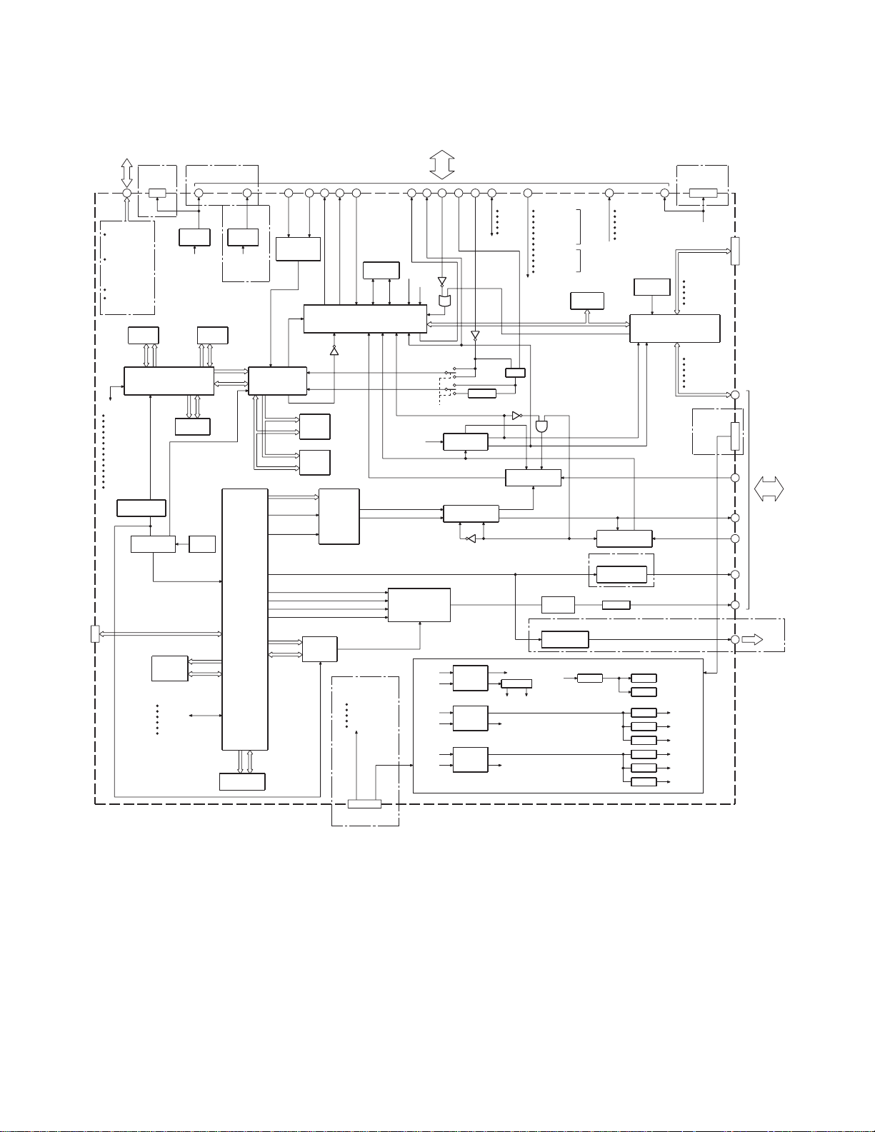
BLOCK DIAGRAM
(X35- )
TOUCH
LCD
(X16- )
SMALL
DISPLAY
REMOTE
CONTROL
RECEIVER
KEY
DVD
MECHA
SLIDE
MECHA
(X34- )
(X14- )
TOUCH
CONTROL
INVERTER
CIRCUIT
SRAM
SDRAM
FLASH
SDRAM
MOTOR
DRIVER
MPEG
DECODER
SH-3
u-COM
SYSCON SDRAM
CLOCK
GENERATOR
FLASH
CPLD
AUDIO
DAC
GRAPHIC
SPDIF
(X89- )
TIMING
CONTROLLER
CHROMA
GAMMA IC
RGB SW
VIDEO
ENCODER
COMPOSITE
SW
SW
TV
I/F
COMPOSITERGB
SW
NAVI
I/F
BOX
u-COM
AM/FM
TUNER
COMPOSITE
SW
I/F
LX-BUS
I/F
DSP
8ch DAC
DIR
ADC
AUDIO
INPUT SELECTOR
AUDIO
OUTPUT
POWER
AMP
AV OUTAV-IN
SP
OUTI/F
SELECTOR
PRE
OUT
3
KVT-817DVD/827DVD/827DVDY
KVT-837DVD/847DVD/867DVD
BLOCK DIAGRAM
● X14-955/956
to X16
2DIN ONLY 1DIN ONLY
to MECHA
/956)
from SYSCOM
LCD CONTROL
LCD CS
LCD DATA
LCD CLK
KEY CONTROL
KEY2
RESET
SRC
EJECT
REMO
LED R,G,B
1DIN ONLY
IC852 IC850
SDRAM
D(15:0) A(19:1) A(22:1) D(15:0)
IC800
SYSCOM
SH CLK
SH MREQ
SH SREQ
SH MDATA
SH SDATA
SH RESET
SH CON
SH STBY
SH INI
SH DACK
GR INT
GR REQ
TOUCH
13.5MHz
TOUCH EN
2 FREQUENCY
DIVIDING
IC640
CLOCK
GENERATOR
27MHz
ATAPI I/F
to DVD
MECHA
(X14-955
SH-3
A(12:4) D(31:0)
IC851
36.864MHz
27MHz
IC560
SDRAM
SYSCOM
BE RST
BE CLK
BE MREQ
BE SREQ
BE MDATA
BE SDATA
RL M+
RL M- EX M-
IC107
MOTOR
DRIVER
TMOTOR M
TMOTOR P
FROM
SRAM
X'TAL
27MHz
A(11:1)
D(15:0)
IC106
MOTOR
DRIVER
SMOTOR M
SMOTOR P
EX M+
PLL CLK
1.5
FREQUENCY
DIVIDING
PLL ON
1DIN ONLY
IC237
DCLK 9.6MHz
GRAPHIC RGB
IC700
A(24:1)
D(31:0)
GRAPHIC
MA(13:0)
MD(15:0)
MA(13:0)
MD(31:16)
IC601 IC652
MPEG
DECODER
A(21:0) D(7:0)
IC520
CCIR601(7:0)
VCLOCK
HSYNC
VSYNC
LA17
LA(1:0)
LD(3:0)
IC750
SDRAM
IC751
SDRAM
IC470
G-HD
G-VD
CDE
CPLD
FLASH
RGB
VCOM
CHROMA GAMMA IC
VIDEO
ENCODER
SPDIF
DATA1
BCLK
LRCLK
MCLK
1DIN ONLY
27MHz
to SYSCOM
ACC DET
REV DET
PRK DET
ILLUMI
REMO
to X35
IC101
E2PROM
1DIN
ONLY
2DIN
ONLY
from SYSCOM
HPOSI1,2,3,4,
NTSC PAL
PWM
MIRROR
LCD PON
IC104
POLS
IC239
1H DELAY
R-Y
to SH3
to SYSCOM
XDATA
BLK
VSY
T/C VD
T/C HD
4.43MHz
3.58MHz
B-Y
HSY
VMUTE
SW D MODE1,2,3
YDATA
AUTO DIMMER
X0
PH DET
X1
R SENS
Y0
SW A,B,C
KEY1
OPEN/CLOSE
KEY3
KEY4
SRC
REMO
EJECT
SCL
SDA
CK
D-FF
DELAY
NAVIL
CP
NTSC PAL
COMPOSITE
RGB
DVDRGB
DVDCOMP V DVDCOMP V
SYNC SEPA
IC650
LPF+6dB AMP
+DRIVER+MUTE
MUTE
IC830
HD
VD
IC240
RGB SW
DVDRGB
RGB SW VIDEO
IC654
VIDEO SW
2DIN ONLY
REG
BUFFER
MUTE
BU3.3V
+B
ACC
GCD
IC402
ADACML
ADACMC
ADACMD
ADACRST
2ch AUDIO DAC
+14.4V
PON
+14.4V
PON
+14.4V
PON SW3.3V
DC/DC
DC/DC
DC/DC
+8.5V
TRANCE
+7.5V
IC400
LPF
1DIN ONLY
OPT DRIVER
+14.4V
-7V+7V
POWER SUPPLY
IC105
RESET IC
MPU
SRAM
REG
REG
REG
REG
REG
REG
SYSCOM
SW5V
V5V
MECHA5V
SW2V
1.9V
1.8V
2DIN ONLY
to SUB PANEL
LED R
LED G
to ROM WRITER
RESET
M CLK
M DATA
S DATA
FROM VPP
to BOX MCU
M CLK
M REQ
S REQ
M DATA
S DATA
SYS ON
2DIN ONLY
+B
ACC
GCD
TV/NAVI RG
DOWNMIX
AUDIO
OPT
OUT
to X34
POWER SUPPLY
CONNECTOR
4

LX I/F
NV I/F
to TV TUN
to X14
ISO AMP
IC500
ISO AMP
IC405
IC413
AUDIO
IC414
SEL
SEL
AUDIO
R SW
IC400-402
G SW
B SW
SEL
VIDEO
IC416
VIDEO
SEL
IC406
IC415
SEL
VIDEO
6dB AMP
VIDEO SEL
IC408
75 DRIVER
DRIVER
6dB AMP
VIDEO SEL
75
IC407
SEL
VIDEO
IC404
FM AM F/E
FST
BUFF
RDS
IC251
DECODER
ADJUST
LEVEL
MUTE
MUTE
ADJUST
LEVEL
MUTE
ADJUST
LEVEL
IC151
ADJUST
LEVEL
TONE
EQ
ADC(2ch)
IC7
MUTE
DIR SEL
IC10
DSP
IC9
S/P DIF
DAC(8ch)
IC6
BASS
MANAGEMENT
IC12
LPF
IC2-4
REG
REG
REG REG
POWER
AMP
IC100
DC
MUTE AMP
IC200-202 PRE OUT
AV OUT
MUTE
AV IN1
ISO AMP
IC204
AV IN2
ISO AMP
IC203
R-CAM
SEP
IC403
SYNC
MCU
IC303
SW
REG
REG
REG
REG REG
REG
SW
LX CON
LX CLK
LX DATA M
LX DATA S
LX REQ S
LX MUTE
LX RST
LX REQ M
AUD Lch
AUD Rch
A GND
REMO
SYNC
G
A GND
R
AUD Lch
AUD Rch
TX
RX
B
TV DATA M
TV DATA S
TV REQ S
TV REQ M
COMP V
B
M RST
R
G
TV CLK
TV CON
TV Rch
A GND
TV Lch
COMP V
DVD Rch
DVD Lch
A GND
B
G
R
M REQ S
M REQ M
M DATA S
M DATA M
M RST
M CLK
M CON
REMO
8
MCU
32
2
MCU
3
3
3
6
MCU
3
6
MCU
3
DVD COMP
3
MCU
2
MCU
2
MCU
1
MCU
2
MCU
MCU
2
MCU
1
MCU
2
MCU
2
RDDA
RDCL
QUAL
MPX for RDS
MCU
S-METER
IF COUNT
SDA
SCL
RDS MUTE
QUALITY
4
MCU
PON AM
A OUT
3
MCU
ACIN0
(FRONT)
ACIN1
(REAR)
FRONT
HPF
(FRONT) (FRONT)
MUTE VOL
(FRONT)
(SUB-W)
ACIN2R
ACIN2L
(CENTER)
MUTE
(REAR)
REAR
(REAR)
HPF VOL
(REAR)
SUB
MAIN
2ZONE
2ZONE
(CEN
MUTE
/NF L
(NF)
LPF
VOLCENTER
SUB-W SUB) SUB)
(CEN
(FRONT)
PAOUT0
(REAR)
PAOUT1
LDOUT1
(REAR)
LDOUT0
(FRONT)
(CEN/NF)
LDOUT2L
(SUB/NF)
LDOUT2R
OUTPUT SEL
TUNE
AUX
CDCH
CD
MD
MAIN
INPUT SEL
SUB
AUX
VOL IN
SCL
SDA
S-MUTE
DCERR
MCU
4
5VDSPA8V
DSPD5V
3.3V
1.25V
3.3V
4
MCU
SVR
BEEP
MUTE
STBY
RR+ -
RL+ -
FR+ -
FL+ -
IC2VI
P.CON
SMALL
GND
BU
EXT.CONT
LINE MUTE
ATT. CO N
SP OUT
8
FRONT L
FRONT R
REAR L
REAR R
CENTER
SUB-W
R
V
L
MCU
MCU
R
L
V
R
L
V
V
MCU
2
BU
SW14V
PON SW14V
BU
A8V
SW14V
BU
V5V
BU
SW14V
DSPA8V
SW14V
BU
DSPD8V
DSPD5V
BU SW5V
BU5V PON
MCU
X89 (DSP)
POWER SUPPLY
POWER SUPPLY
5
● X34-355/381
BLOCK DIAGRAM
KVT-817DVD/827DVD/827DVDY
KVT-837DVD/847DVD/867DVD
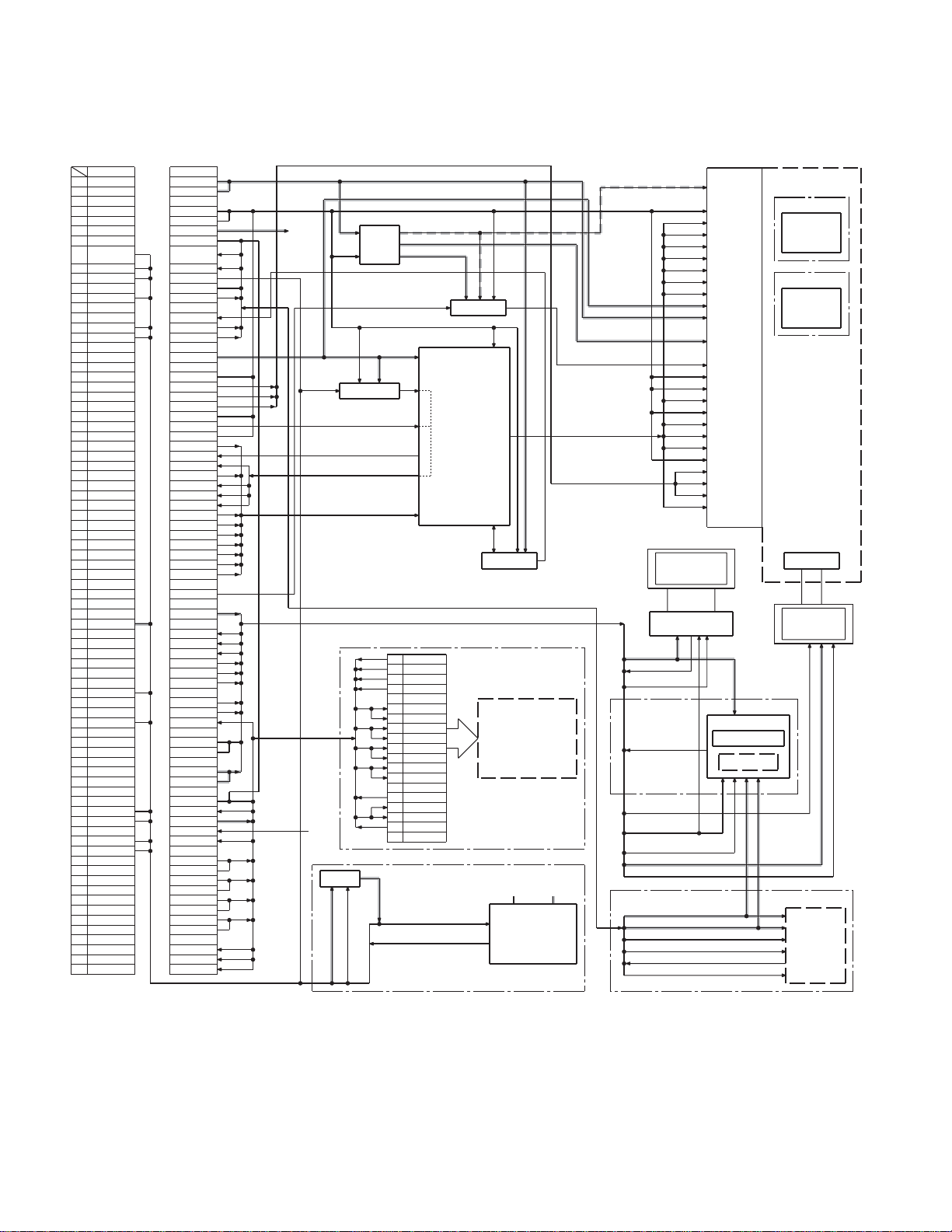
KVT-817DVD/827DVD/827DVDY
KVT-837DVD/847DVD/867DVD
BLOCK DIAGRAM
● X35-448/449
2DIN TYPE 1DIN TYPE
1
PON+5.0V
2
PON+5.0V
3
NC
4
VGND
5
VGND
6
SW+18.5V
7
DGND
8
EJECT
9
KEY3
10
KET4
11
LED GND
12
SI
13
NC
14
PLL CLK
15
LED G
16
LED R
17
NC
18
PON+3.3V
19
NC
20
VGND
21
VB
22
VG
23
VR
24
VGND
25
T/C HD
26
V GND
27
NTSC/PAL
28
PLL ON
29
POLS
30
MIRROR
31
VSY
32
HSY
33
BLK
34
MODE3
35
MODE2
36
MODE1
37
HPOS4
38
HPOS3
39
HPOS2
40
HPOS1
41
NC
42
VCOM
43
NC
44
PON+3.3V
45
BU+3.3V
46
NC
47
XDATA
48
YDATA
49
X0
50
X1
51
Y0
52
SRC
53
PWM
54
ENABLE
55
T/C VD
56
NC
57
BL GND
58
BL GND
59
NC
60
BL +8.5V
61
BL +8.5V
62
NC
63
NC
64
ESD GND
65
ESD GND
66
BL DET
67
RESET
68
REMO
69
70
71
72
73
74
75
76
77
78
79
80
PON+5.0V
PON+5.0V
NC
VGND
VGND
SW+18.5V
DGND
OPEN
CLOSE
NC
T/C VD
LED GND
BRINK
NC
PLL CLK
LED G
LED R
NC
PON+3.3V
NC
VGND
VB
VG
VR
VGND
T/C HD
V GND
NTSC/PAL
PLL ON
POLS
MIRROR
VSY
HSY
BLK
MODE3
MODE2
MODE1
HPOS4
HPOS3
HPOS2
HPOS1
NC
VCOM
NC
PON+3.3V
AUTO DIM
KEY1
XDATA
YDATA
X0
X1
Y0
NC
PWM
ENABLE
SW-D
NC
BL GND
BL GND
NC
BL +8.5V
BL +8.5V
NC
DGND
PH DET
SW+5.0V
BL DET
RSENS
NC
RI MRI MRI M+
RI M+
EX MEX MEX M+
EX M+
NC
SW-A
SW-B
SW-C
OPEN
IC302
POLS/HSY/VSY/BLK
MODE1/2/3/HPOS1/2/3/4
NTSC/PAL,MIRROR
OPEN
TR SW
BU3.3V
SI
VR/VG/VB
PON+5.0V
PON+3.3V
VGND
IC101
DC-DC
IC
VCOM
VGND
PON+3.3V
SI3.3V
PON-12.0V
PON+18.5V
PON+12.5V
IC203
COM AMP
IC301
TIMMING
CONTROLLER
PDOS/OSCI
IC303
SW-D
1
SW-C
2
SW-B
3
SW-A
4
NC
5
EX M+
6
EX M+
7
EX M-
8
EX M-
9
RI M+
10
RI M+
11
RI M-
12
RI M-
13
NC
14
RSENS
15
16
REF+5.0V
17
SW+5.0V
18
PH DET
19
NC
LED_G,LED R,SI3.3V
RESET,SRC,EJECT,KEY3
KEY4,REMO.ESD GND
PLL & LPF
1DIN ONLY
7 INCH
INDASH MECHA
2DIN ONLY
D GND PON+5.0V
SW PCB
PON-12.0V
VGND
PON+3.3V
PON+5.0V
PON+18.5V
V.COM
UPSD/CPV/ HDIR/CX/
STV1/STV2/STH1/STH2/
NGOE1/NGOE2/
NGOE3/CPH1
PON+5.0V
XDATA/YDATA
X0/X1/Y0
AUTO DIM/
KEY1
PWM/ENABLE
D.GND
LED GND
BL8.5V
BL GND
LED+8.5V(B)
LED+8.5V(R)/LED+8.5V(G)
LED GND
DGND
OPEN CLOSE/VOL+/VOLBRINK
VGL-12.0V
STV1
UPSD
U/D(UPSD)
CPV
NGOE3
OE3(NGOE3)
NGOE2
OE2(NGOE2)
NGOE1
OE1(NGOE1)
STV2
VDD1+3.3V
VDD2+5.0V
VGH+18.5V
CPH1
CPH(CPH1)
CX
HDIR
L/R(HDIR)
STH1
VB
VG
VR
STH2
TOUCH PANEL
X0/X1/
Y0/Y1
TOUCH PANEL
SWITCH CIRCUIT
IC401
AUTO DIMMER
NC
NC
VSS
STV1
CPV
STV2
NC
NC
VCOM
VSS
VSS
VSS
CX
STH1
VSS
VB
VG
VR
STH2
NC
1DIN ONLY
SW PCB B/3
2DIN ONLY
6.5 INCH
LCD
1DIN ONLY
7 INCH
LCD
0.5mm
30PIN
CFL
BACK LIGHT
INVERTER
1DIN ONLY
SW PCB
C/3
6
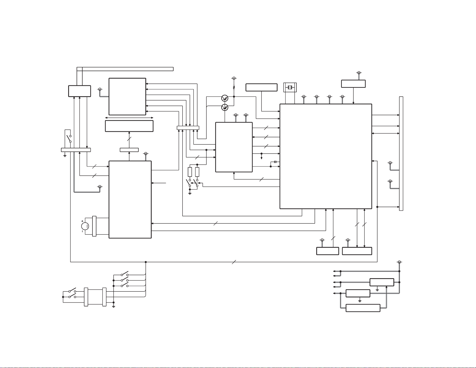
MOTOR
SPINDLE
PICK UP
OPTICAL
STEPPING MOTOR
2 PHASE
M
CONNECTOR
(18P,0.5PITCH)
(24P,0.5PITCH)
CONNECTOR
CONNECTOR
(10P,0.5PITCH)
(2P,PIN ASSY)
CONNECTOR
ACTUATER
DRIVER
IC2
PROCESSOR
FRONT END
APC TR
Q7,Q8
Q1,Q2
THERMISTER
RESET IC
IC4
EEPROM
IC11
FLASH ROM
IC3
(50P,0.5PITCH)
CONNECTOR
DISC CONTROLLER
OPTICAL
(4P,0.5PITCH)
CONNECTOR
3.3V REG.
IC10
A3.3V
D3.3V
D5V
A5V
IC9
1.5V REG.1.5V
VOLT AGE DET
IC8
IC5
MOTOR &
IC1
CN4
CN3
CN2
CN1 CN5
CN6
CN1
HALL BIAS
HALL SENSOR
U,V,W, COIL
DVD LD/CD LC
VC (2.2V)
MODE SW/GAIN SW
FO+-,TR+-
PD/VR DVD/VR CD
I/V OUT (DVD/CD)
4
3
7
P5V
P5V
DC MOTOR
LO/EJ
3PHASE
PWM
PWM*2
VHALF
8
A,B,C,
D,E,F,RF (P,N)
SCK,STDI
SEN
9
2
3
7
VHALF
A5V
ARF,NARF
FBAL
JLINE,TSTSG
FE,AS,REFNV,RFDIFO
OFTR,BDO,VREF2
VHALF (16.5V)
TRCRS
TE
DVDON/CDON
SEN
SCK,STDI
A3.3VA5V
A3.3V
DISC
A3.3VD5V 1.5VD3.3V
IOP- (AD)
TEMP DET (AD)
16.897849MHz
D3.3V
GAIN SW
PWM8,DRV.MUTE,LO.MTE,B
SPDRV,FODRV,TRDRV
MS,STEP A,STEP B
FG,EXCNT1
SDA,SCL
FADR0-FADR17,
NCE,NWE,NOE
FDT0-FDT7
D3.3V
2
D3.3V
821
S/P DIF
AUDIO OUT
CD-DA
ATAPI IF
D5V
P5V
DISC DET
6
A
B
D
E
C
D5V
LIM SW
FG
VREF,EC
PWM*2
SW A,B,C,D,E
LIM-SW
NRST
VR
FFC
3
● X37-107 (DVD mechanism)
BLOCK DIAGRAM
KVT-817DVD/827DVD/827DVDY
KVT-837DVD/847DVD/867DVD
7

KVT-817DVD/827DVD/827DVDY
KVT-837DVD/847DVD/867DVD
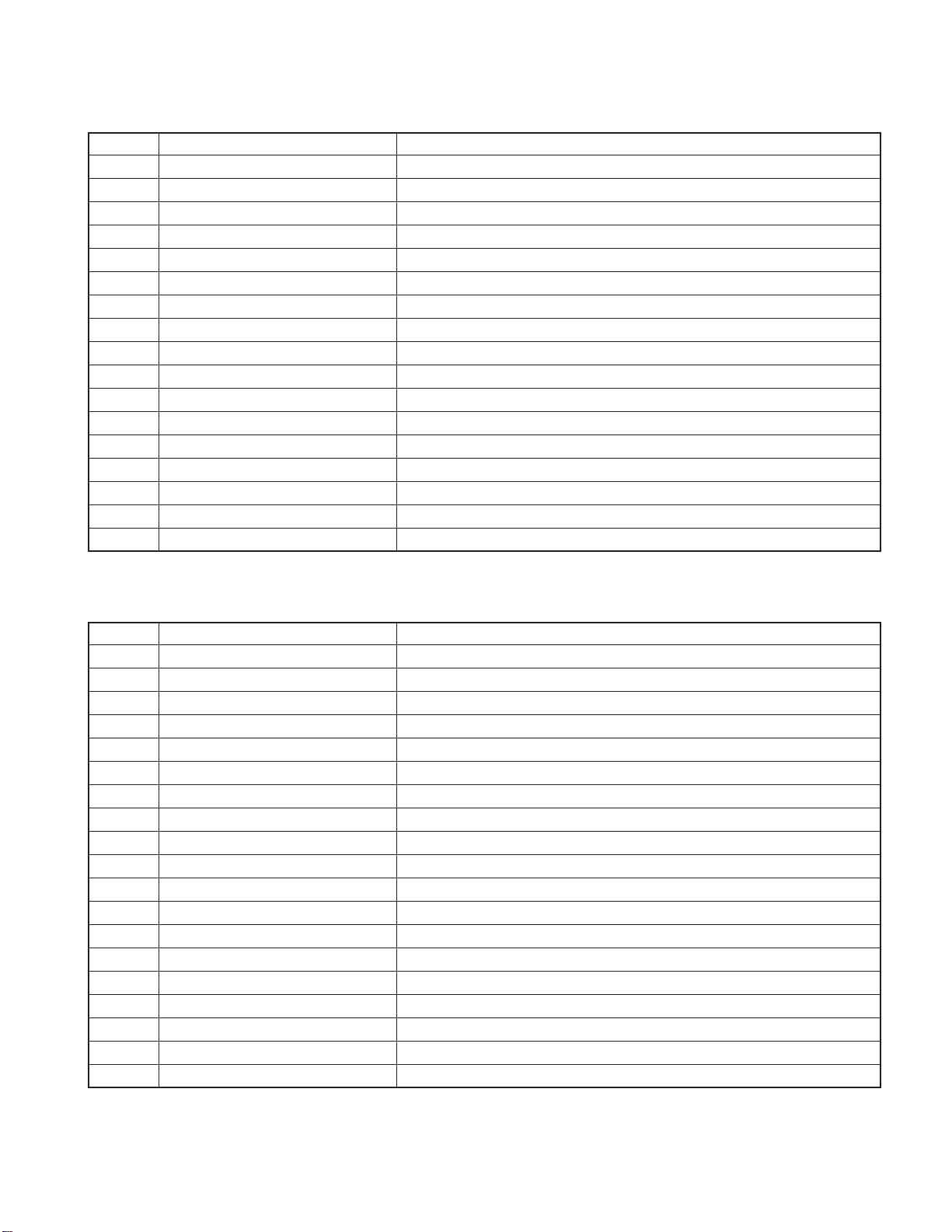
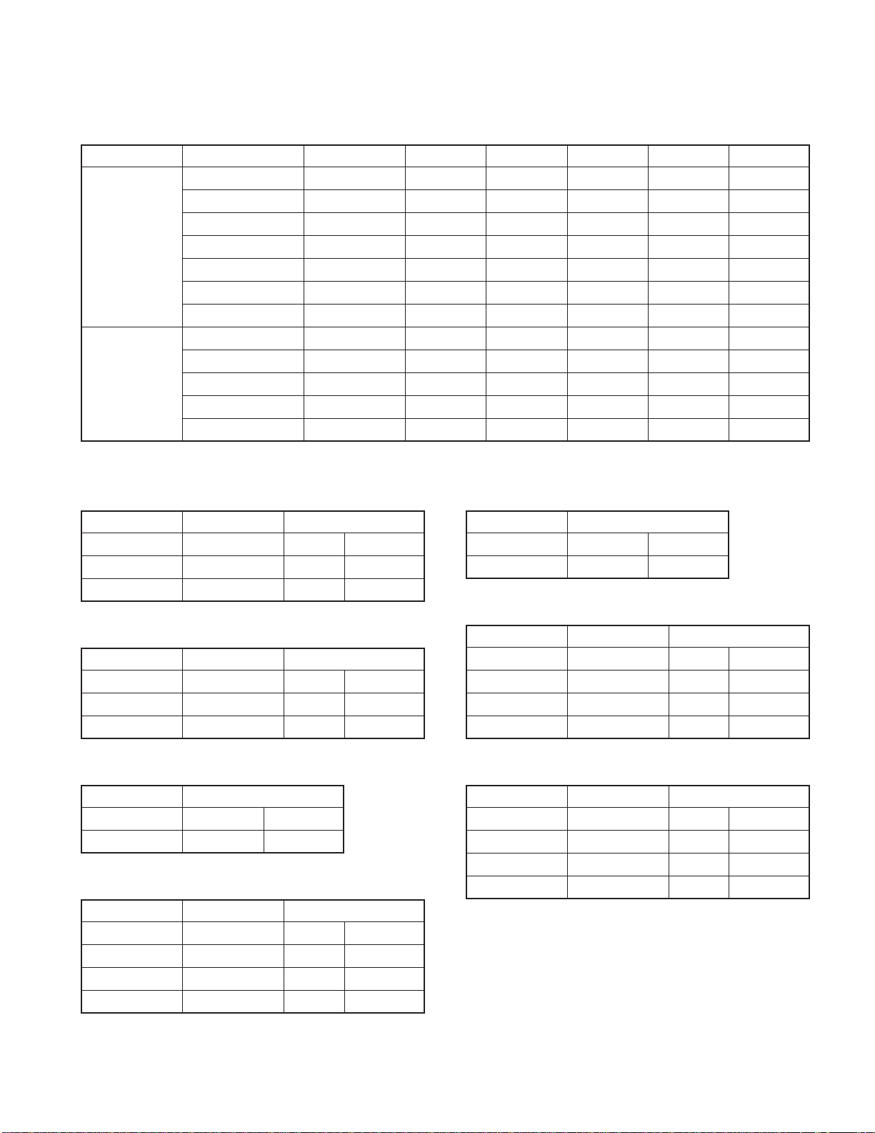
COMPONENTS DESCRIPTION
● VIDEO CONTROL UNIT (X14-955/956x-xx)
Ref. No. Application / Function Operation / Condition / Compatibility
IC1 DC-DC power supply IC For controlling BL8.5V and ±7V
IC2 DC-DC power supply IC For controlling SW6.5V and MECHA7.5V
IC3 DC-DC power supply IC For controlling SW3.3V and SW2.5V
IC9 Regulator IC 2V generation for IC601
IC80 Regulator IC Backup 3.3V generation
IC81 Regulator IC SW5V generation
IC82 Regulator IC V3.3V generation
IC101 E2PROM Memory for µ-com
IC103 Logic IC (AND) AND for remote controller and wired remote controller
IC104 µ-com IC For controlling the main unit
IC105 Resetting IC For resetting µ-com
IC106 Motor driver IC Sliding control of sliding mechanism
IC107 Motor driver IC Angle control of sliding mechanism
IC108 Logic IC (AND∗4) 3.3V → 5V conversion
IC237
IC238 Logic IC (Inverter) For blank signal reversal coming from X35
IC239 Color differentiation signal 1H-DELAY For delaying 1H color differential signals when PAL
IC240 RGB switch For switching RGB signals coming from DVD signal and X34
IC400 Ope amp IC For audio LPF
IC401 Regulator IC 5V generation for audio
IC402 Audio DAC For converting digital signals into analog signals
IC403 Logic IC (Inverter) SPDIF driver
IC470 CPLD Audio DAC control
IC500 Regulator 5V generation for DVD mechanism
IC520 FLASH ROM For MPEG decoder control program
IC560 SDRAM RAM for temporary storage of decoded signal
IC601 MPEG decoder IC for decoding MPEG encoded signal
IC640 Clock generator 27M, 36.864MHz clock generation
IC641 Logic IC (D-FF) 13.5MHz is generated by frequency dividing from 27MHz
IC650 LPF and Driving IC for video signal For RGB and composite signals of DVD
IC651 Regulator V5V generation
IC652 Video encoder Conversion of digital video signals into analog signals
IC654 Video switch For switching DVD composite signal and composite signal from X34
IC700 GRITT IC Graphic signal generation
IC701 Regulator IC700 1.8V generation
IC750,751 SDRAM GRITT-IC storage RAM
IC770 Logic IC (NOR) GRITT-IC video clock frequency dividing
IC771 Logic IC (D-FF∗4) GRITT-IC video clock frequency dividing
IC772 Logic IC (Inverter) GRITT-IC video clock frequency dividing
IC773 Logic IC (AND) GRITT-IC video clock frequency dividing
IC774 Logic IC (OR) GRITT-IC video clock frequency dividing
Signal processing IC for driving color
liquid crystal panel
RGB signal generation for liquid crystal
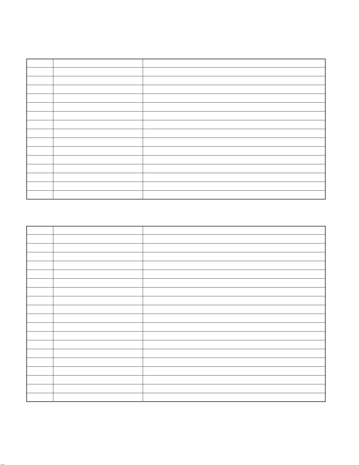
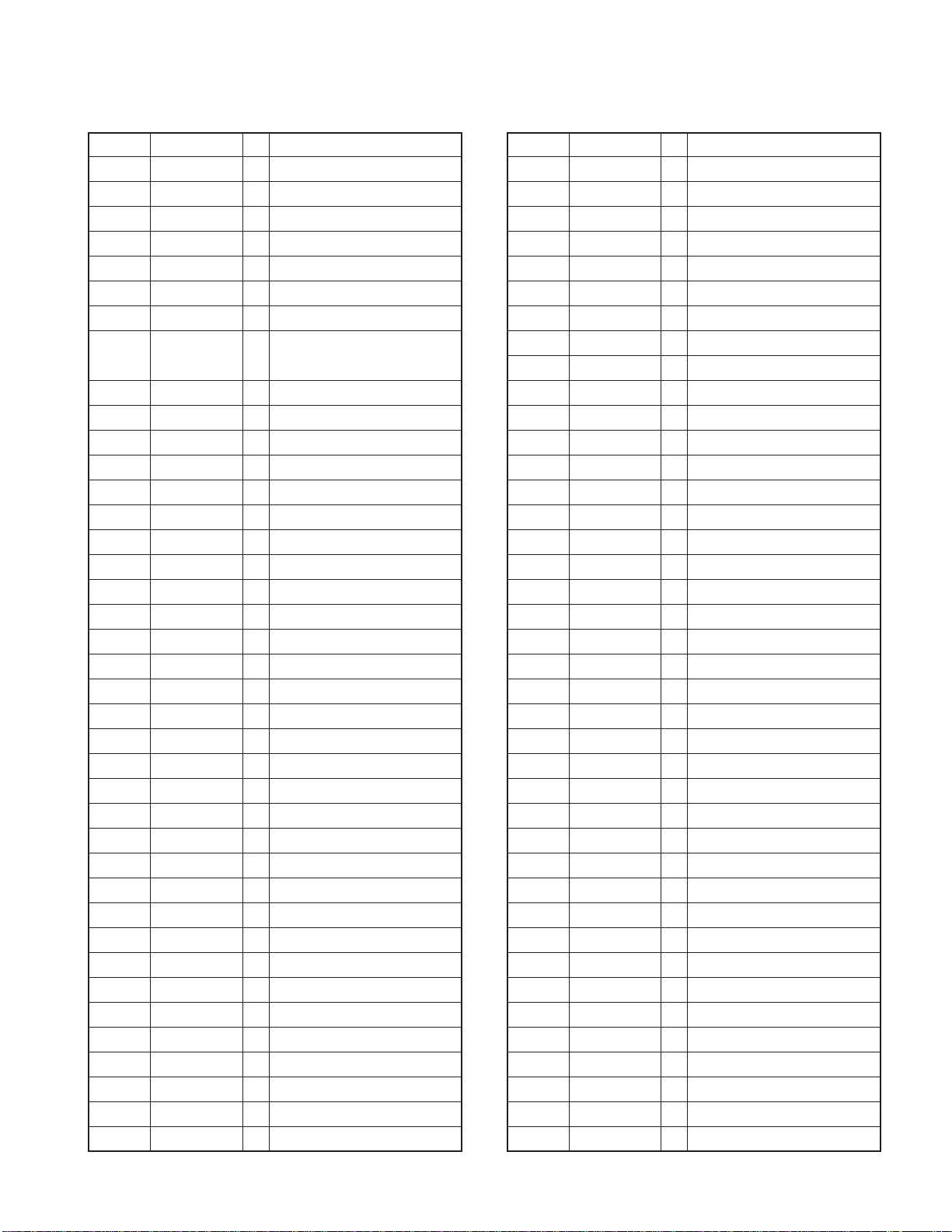
8

KVT-817DVD/827DVD/827DVDY
KVT-837DVD/847DVD/867DVD
COMPONENTS DESCRIPTION
Ref. No. Application / Function Operation / Condition / Compatibility
IC779 Logic IC (NAND) GRITT-IC video clock frequency dividing
IC781 Logic IC (Inverter) For reversing switching used for graphic signal and other signals
IC800 SH-3 µ -com For GRITT-IC control
IC801 Regulator IC800 1.9V generation
IC830
IC831 Logic IC (Inverter) For reversing GRITT-IC HD
IC832 Logic IC (D-FF) For GRITT-IC VD generation when using NAVI
IC833 Logic IC (D-FF) VD generation for µ-com input
IC834 Logic IC (Inverter∗3) For reversing IC830 output HD
IC835 Logic IC (Data selector∗4) For HD/VD selection for GRITT-IC (NAVI or otherwise)
IC836 Logic IC (AND) VD buffer for IC237/timing control
IC850 FLASH ROM For SH-3 µ-com program
IC851 SRAM SH-3 µ-com RAM
IC852 SDRAM SH-3 µ-com RAM
IC853 Logic IC (AND) For SRAM control
IC854 Logic IC (BUS SWITCH) SRAM control
IC855 Logic IC (Inverter) SRAM control
Q1 Small signal NPN transistor For ACC detection
Q2 PNP digital transistor For PARK detection
Q3 NPN digital transistor For SW 14.4V control
Q4 Small signal NPN transistor For DC-DC external oscillation frequency input clamp
Q5 Small signal PNP transistor For temperature compensation of DC-DC external oscillation frequency input clamp
Q6 FET For SW 14.4V control
Q9 NPN digital transistor For DC-DC oscillation frequency switching
Q13 FET For BL8.5V and ±7V generation
Q16 NPN digital transistor For DC-DC oscillation frequency switching
Q18 NPN digital transistor For MECHA7.5/5V switching
Q19 FET For SW6.5V/MECHA7.5V generation
Q20 NPN digital transistor For DC-DC oscillation frequency switching
Q22 FET For SW3.3V/SW2.5V generation
Q23 NPN digital transistor
Q24 Small signal NPN transistor For DC-DC external oscillation frequency input clamp
Q25 PNP digital transistor
Q26 Small signal NPN transistor For DC-DC external oscillation frequency input clamp
Q27 PNP digital transistor
Q80 NPN digital transistor For reduced/excess current detection circuit
Q81 Small signal NPN transistor For reduced/excess current detection circuit
Q82 Small signal PNP transistor For reduced/excess current detection circuit
Q83 Small signal NPN transistor For reduced/excess current detection circuit
Q84 PNP digital transistor For reduced/excess current detection circuit
Q85 Small signal NPN transistor For reduced/excess current detection circuit
Q86 Small signal PNP transistor For reduced/excess current detection circuit
Q87 PNP digital transistor For reduced/excess current detection circuit
PLL built-in synchronization separation IC
HD/VD generation from composite signal by synchronization separation
For REF voltage impulse at the time of DC-DC external oscillation frequency input stoppage
For REF voltage impulse at the time of DC-DC external oscillation frequency input stoppage
For REF voltage impulse at the time of DC-DC external oscillation frequency input stoppage
9

KVT-817DVD/827DVD/827DVDY
KVT-837DVD/847DVD/867DVD
COMPONENTS DESCRIPTION
Ref. No. Application / Function Operation / Condition / Compatibility
Q88
Q89~91 Small signal NPN transistor 8.5V regulation circuit for BU3.3V
Q92 Small signal PNP transistor 8.5V regulation circuit for BU3.3V
Q93 NPN digital transistor For reduced/excess current detection circuit
Q94 PNP digital transistor For SW14.4V control
Q95
Q101 NPN transistor For BLUE_LED control
Q102 PNP digital transistor For BLUE_LED control
Q103 NPN digital transistor For GREEN_LED control
Q104 PNP digital transistor For GREEN_LED control
Q105 NPN digital transistor For RED_LED control
Q106 PNP digital transistor For RED_LED control
Q107 PNP digital transistor For resetting
Q108 NPN digital transistor For resetting
Q109 Small signal PNP transistor For switching µ-com AD conversion reference voltage BU3.3V/SW3.3V
Q110 NPN digital transistor For switching µ-com AD conversion reference voltage BU3.3V/SW3.3V
Q111 Small signal PNP transistor For switching µ-com AD conversion reference voltage BU3.3V/SW3.3V
Q112,113 Small signal NPN transistor For switching µ-com AD conversion reference voltage BU3.3V/SW3.3V
Q114 PNP digital transistor For resetting
Q115 NPN digital transistor For setting to OV until setting is completed, immediately after resetting µ-com 20 pin
Q170,171 Small signal PNP transistor µ-com input voltage 5V → 3.3V conversion
Q172,173 Small signal NPN transistor µ-com input voltage 5V → 3.3V conversion
Q230 Small signal NPN transistor For input video signal clamp to IC237
Q231 Small signal NPN transistor For brightness signal input buffer to IC237
Q232 Small signal PNP transistor For color signal input buffer to IC237
Q233 NPN digital transistor For IC240 switching control
Q234 Small signal PNP transistor For switching at the time of chroma trap PAL
Q236 Small signal NPN transistor For IC237 3V generation
Q237 Small signal PNP transistor For IC237 3V generation
Q238,239 Small signal NPN transistor For IC237 7.5V generation (7.5V fluctuates a little.)
Q240 Small signal PNP transistor For IC237 7.5V generation (7.5V fluctuates a little.)
Q400,401 Small signal NPN transistor For audio signal muting
Q402 Small signal NPN transistor For audio signal muting control
Q403 NPN digital transistor For audio signal muting control
Q404,405 PNP digital transistor For audio signal muting control
Q650 PNP digital transistor Resetting 3.3V → 5V conversion for IC652
Q651 NPN digital transistor Resetting 3.3V → 5V conversion for IC652
Q652 NPN digital transistor For reversing RGB_SW
Q653 NPN digital transistor For DVD composite muting
Q700 Small signal PNP transistor For GRITT-IC video signal reference voltage generation
Q701 Small signal NPN transistor For GRITT-IC video signal reference voltage generation
PNP transistor for low-frequency power
amplification
NPN transistor for low-frequency
general amplification∗2
8.5V regulation circuit for BU3.3V
For SW14.4V control
10
KVT-817DVD/827DVD/827DVDY
KVT-837DVD/847DVD/867DVD
COMPONENTS DESCRIPTION
Ref. No. Application / Function Operation / Condition / Compatibility
Q771,772 Small signal NPN transistor For GRITT-IC video clock amp
Q830 PNP digital transistor NT/PAL control 3.3V → 5V conversion for IC830
Q831 NPN digital transistor NT/PAL control 3.3V → 5V conversion for IC830
Q901 NPN digital transistor For ILLUMI detection
Q902 NPN digital transistor For REVERSE detection
Q904 Small signal NPN transistor SW3.3V control for X16
Q905
Q906 NPN digital transistor SW5V control for X16
Q907 PNP digital transistor SW5V control for X16
Q908 NPN digital transistor SW5V control for X16
● SUB-CIRCUIT UNIT (X16-303/304x-xx)
Ref. No. Application / Function Operation / Condition / Compatibility
IC201 Remote controller light receptor section Remote controller light receptor section
Q101 For DSI signal switching DSI signal control
Q204 For LED switching Switching LED_Blue / LED Green on MINI_LCD
Q205 For LED switching Switching LED_Blue / LED Red on MINI_LCD
Q206 For LED switching Switching LED_Red /LED_Green
PNP transistor for medium power
amplification
SW3.3V control for X16
● ELECTRIC UNIT (X34-355/381x-xx)
Ref. No. Application / Function Operation / Condition / Compatibility
IC50 3-terminal regulator IC 8.4V for audio is generated from BU 14V
IC51 3-terminal regulator IC DSP audio 8.4V generation from BU 14V
IC52 Power supply conversion IC ±9.0V for 5V pre-out is generated from BU14V
IC53 3-terminal regulator IC DSP digital 5V generation from DSP digital 8V
IC54 3-terminal regulator IC 5V for video is generated from BU14V
IC100 Power IC Power amplifier for speaker output
IC150 Operational amplifier Audio mid-point electrical potential 3.3V, SVR voltage 6.8V buffer
IC151 Electrical volume and Selector IC Audio volume control, audio signal selection
IC200 Operational amplifier For 5V pre-out audio signal amplification (Front)
IC201 Operational amplifier For 5V pre-out audio signal amplification (Rear)
IC202 Operational amplifier For 5V pre-out audio signal amplification (Center, Sub-woofer)
IC203 Isolation amplifier IC For audio signal GND isolation (AVIN2)
IC204 Isolation amplifier IC For audio signal GND isolation (AVIN1)
IC251 RDS decoder IC For RDS signal processing and demodulation
IC300 Voltage detector For µ-com resetting voltage monitoring
IC301 Logic IC (NOR) Muting control for audio
IC303 Audio microcomputer For X34 board control
IC400 Video switch For video signal selection (R)
IC401 Video switch For video signal selection (G)
11

KVT-817DVD/827DVD/827DVDY
KVT-837DVD/847DVD/867DVD
COMPONENTS DESCRIPTION
Ref. No. Application / Function Operation / Condition / Compatibility
IC402 Video switch For video signal selection (B)
IC403 Synchronization separation IC For NT/PAL recognition, AVIN/Rear camera auto detection
IC404 Video switch Video signal selection (Synchronization separation)
IC405 Isolation amplifier IC For audio signal GND isolation (TV)
IC406,407 Video switch Video signal selection (For monitoring main unit)
IC408 Video switch Video signal selection (For AVOUT)
IC413 Logic IC (Multiplexer) For audio signal selection (For MAIN source)
IC414 Logic IC (Multiplexer) For audio signal selection (For 2-ZONE sources)
IC415 Video switch Video signal selection (For monitoring main unit)
IC416 Video switch Video signal selection (For AVOUT)
IC500 Isolation amplifier IC For audio signal GND isolation (LX)
IC501 Logic IC (Inverter) For reversing resetting signal
IC502 Logic IC (Buffer) Buffer for remote control signal for NAVI
Q1 For fan 11V power supply Comes ON when Q2 is ON
Q2 For fan 11V power supply Comes ON when Q3 is ON
Q3 For fan 11V power supply Comes ON when SW5V is ON
Q4 For fan 11V power supply For controlling output voltage
Q6 For ANT-CONT SW Comes on when TUNER source is selected
Q7 For P-CONT SW Goes OFF when STANDBY source is selected
Q8~11 For P-CONT circuit control Controlling P-CONT circuit
Q12 BU detection SW Comes ON power supply voltage is about 8.8V or more
Q13 For EXT-AMP control Control of external amplifier
Q14 For surge voltage detection Comes ON when Q15 is ON
Q15 For surge voltage detection Comes ON when power supply voltage is about 20V or more
Q50 For ±9V power supply Comes ON when Q51 is ON
Q51 For ±9V power supply Comes ON when SW14V is ON
Q52 SW 14V power supply SW Comes on at P-ON
Q53 For DSP digital 8V power supply
Q54 For BU 5V power supply
Q55 A8V power supply SW Comes ON when SW14V is ON
Q56 DSP analog 8V power supply SW Comes ON when SW14V is ON
Q57 For DSP digital 8V power supply
Q58 For BU 5V power supply
Q59 For A8V power supply BU 14V → 8V for audio is supplied
Q60 For DSP analog 8V power supply BU 14V → Supply DSP analog 8V
Q61 V5V power supply SW Comes ON when SW14V is ON
Q62 SW 5V power supply SW Comes ON at P-ON
Q63 For SW 5V power supply BU 5V → SW 5V is supplied
Q64 For V5V power supply BU 14V → 5V for video is supplied
Q65~70 For ±9V power supply
Q150
Q151 For SVR voltage reduction control Electric current control of SVR voltage reduction circuit
SVR6.8V, Audio 3.3V,
IC150 power supply SW
Comes ON when SW14V is ON
12
KVT-817DVD/827DVD/827DVDY
KVT-837DVD/847DVD/867DVD
COMPONENTS DESCRIPTION
Ref. No. Application / Function Operation / Condition / Compatibility
Q152
Q200 For audio muting Audio muting of pre-out front right channel
Q201 For audio muting Audio muting of pre-out front left channel
Q202 For audio muting Audio muting of pre-out rear left channel
Q203 For audio muting Muting at momentary power down, resetting, and audio mute timing
Q204 For audio muting Audio muting of pre-out rear right channel
Q205 For audio muting Audio muting of pre-out center channel
Q206 For audio muting Audio muting of pre-out sub-woofer channel
Q207 For audio muting Audio muting of AVOUT right channel
Q208 For audio muting Muting at momentary power down, resetting, and audio mute timing
Q209 For audio muting Audio muting of AVOUT left channel
Q250 AM power supply SW Comes ON when AM source is selected
Q252 For AM power supply Audio 8V is supplied when AM source is selected
Q403,404 Audio selector control SW Converts IC413 µ-com controlled terminal voltage: 5V → 8V
Q405,406 Audio selector control SW Converts IC414 µ-com controlled terminal voltage: 5V → 8V
Q500 For reversing resetting signal voltage Reverses signal in order to obtain resetting signal for TV tuner
Q800 MUTE 0 terminal control SW MUTE 0 audio muting control
SVR6.8V, Audio 3.3V, IC150 power supply
Power supply to IC150, voltage supply to Q151
● VIDEO UNIT (X35-448/449x-xx)
Ref. No. Application / Function Operation / Condition / Compatibility
IC1 Inverter control IC Control and drive of inverter circuit for backlight
IC101 DC/DC converter IC ±12V power supply for VCOM amp, -12.0V/+18.5V LCD power supply
IC203 VCOM amp VCOM signal amplification amp
IC300 Three states buffer Start pulse switching SW
IC301 Timing controller IC LCD module control
IC302 AND V.SYNC delay buffer
IC303 PLL LPF LPF for PLL control (VT voltage control)
IC401 Dimmer sensor IC Auto Dimmer detection sensor
Q1 Dimmer SW ON/OFF control signal of PWM and put on dimmer on backlight
Q2,3 Inverter driver Inverter circuit driving
Q5 5V AVR 5V power supply for inverter control IC
Q202,203 VCOM driver VCOM signal buffer
Q300 Switch For switching IC205
Q301 VCO For PLL oscillation
Q302,303 Buffer For PLL clock
Q501 Touch panel Y1 SW
Q502 Touch panel X0/Y1 SW Y1 SW: Comes ON when inputting to Y-axis and impresses voltage
Q503 Touch panel X1/Y0 SW X1 SW: Comes ON when detecting panel touch/X-axis input and impresses voltage
Q601 Switch OPEN/CLOSE key ILLUMI blinking switch
Y0 (X0) SW: Comes ON when inputting to Y (X)-axis and goes OFF when inputting X (Y)-axis
13
KVT-817DVD/827DVD/827DVDY
KVT-837DVD/847DVD/867DVD
COMPONENTS DESCRIPTION
● DAUGHTER UNIT (X89-274/279x-xx)
Ref. No. Application / Function Operation / Condition / Compatibility
IC2 OP amp For audio signal amplification (Center, Sub-woofer)
IC3 OP amp For audio signal amplification (Rear)
IC4 OP amp For audio signal amplification (Front)
IC5 3-terminal regulator 5V is output from 8V
IC6 Audio DAC D/A conversion of audio signal (Front, Rear, Center, Sub-woofer)
IC7 A/D converter A/D conversion of audio signal (Lch, Rch)
IC9 DSP Processing of computing for Dolby 5.1ch, dts etc.
IC10 DIR Conversion of S/PDIF format data to digital audio format
IC11 OP amp For audio signal amplification (Front)
IC12 Analog switch Switching audio signal (Sub-woofer) and A4V
IC18 Logic IC Inverter for generating clock
IC19 3-terminal regulator 1.25V his output from 3.3V
IC20,21 3-terminal regulator 3.3V is output from 5V
Q13 Digital transistor
Q14,15 Transistor for audio muting
Comes ON at the time of momentary power down, resetting, and in audio muting timing
Comes Mute at the time of momentary power down, resetting, and in audio muting timing
● DVD UNIT (X37-1070-00)
Ref. No. Application / Function Operation / Condition / Compatibility
IC1 RF signal processing IC RF signal processing
IC2 Driver Driver for motorists/pickup actuators
IC3 FLASH ROM FW maintenance for optical DISC control IC
IC4 µ-com built-in optical DISC control IC Optical DISC control in general/ATAPI interface
IC5 Voltage detection IC For reset of optical DISC control IC
IC8 Voltage detection IC For monitoring power supply voltage
IC9 S1.5V power supply IC S5V → S1.5V
IC10 S3.3V power supply IC S5V → S3.3V
IC11 EEPROM Data storage for optical DISC control IC
Q1 MOS-FET DVD laser diode ON/OFF control
Q2 MOS-FET CD laser diode ON/OFF control
Q7 APC transistor CD laser diode light emission amount control
Q8 APC transistor DVD laser diode light emission amount control
Q9 MOS-FET For CD laser diode protection
Q10 MOS-FET For DVD laser diode protection
Q11 Resistor built-in transistor LO-MUTE signal control
Q12 Resistor built-in transistor FG signal control
Q13 Resistor built-in transistor BMS signal control
Q14 Resistor built-in transistor DRMU signal control
14

KVT-817DVD/827DVD/827DVDY
KVT-837DVD/847DVD/867DVD
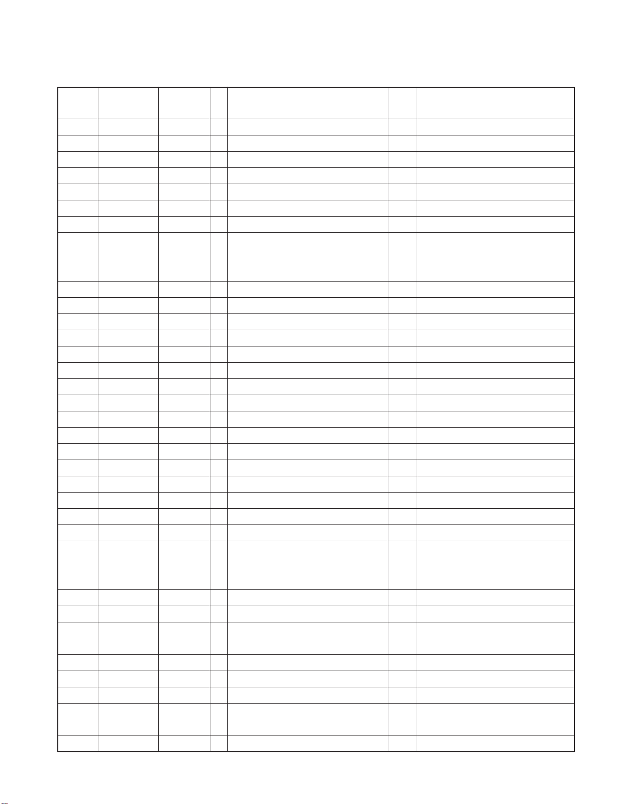
MICROCOMPUTER’S TERMINAL DESCRIPTION
● System Microcomputer: 703264YGJ501A (X14: IC104)
Pin No. Pin Name
1AVREF0
2AVSS
3,4 NC
5AVREF1
6 V_MUTE VIDEO O Video mute H: MUTE ON
7HD VIDEO I Graphic
7NC OOSD
8 FLMD0 µCOM I
9 VDD
10 REGC
11 VSS
12 X1 4.953MHz
13 X2
14 RESET µCOM I
15 XT1 32.768kHz
16 XT2
17 NC
18 VD VIDEO I (Graphic)
18 NC O OSD
19 BU_DET
20 DISK_DET
21 ACC_DET
22 MINI_SDATA PANEL I Data input from mini liquid crystal
23 NC O
24 MINI_CLKIN PANEL I Communication clock with mini liquid crystal
25 BE_MDATA B/E O Data output to B/E-IC
26 BE_SDATA B/E I Data input from B/E-IC
27 BE_CLK B/E I Communication clock with B/E-IC
28 BE_MREQ B/E O Request to B/E-IC
29 BE_SREQ B/E I Request from B/E-IC
30 REMO PANEL I Remote controller
31 S_MUTE VIDEO O Composite signal mute L: FULL GRAPHIC (OSD), H: OTHER
32 NC
33 EVSS
34 EVDD
35 SDA/E2P_SDA µCOM I/O Access with E2P
35
35
36 SCL/E2P_SCL µCOM I/O Access with E2P
36
SDA/ROM_COR_SDA
SDA/CHROMA_SDA_SDA
SCL/ROM_COR_SCL
Module (physical)
Power supply
DVD_MECHA
Power supply
µCOM I/O
Chroma γ I/O Access with chroma γ IC
µCOM I/O
I/O Application Processing Operation Description
I Back up detection H: Reduced electric power detection
I Disk detection L: Disc IN
IACC detection H: ACC reduced electric power detection
Access with E2P at coping with ROM correction
Access with E2P at coping with ROM correction
15

KVT-817DVD/827DVD/827DVDY
KVT-837DVD/847DVD/867DVD
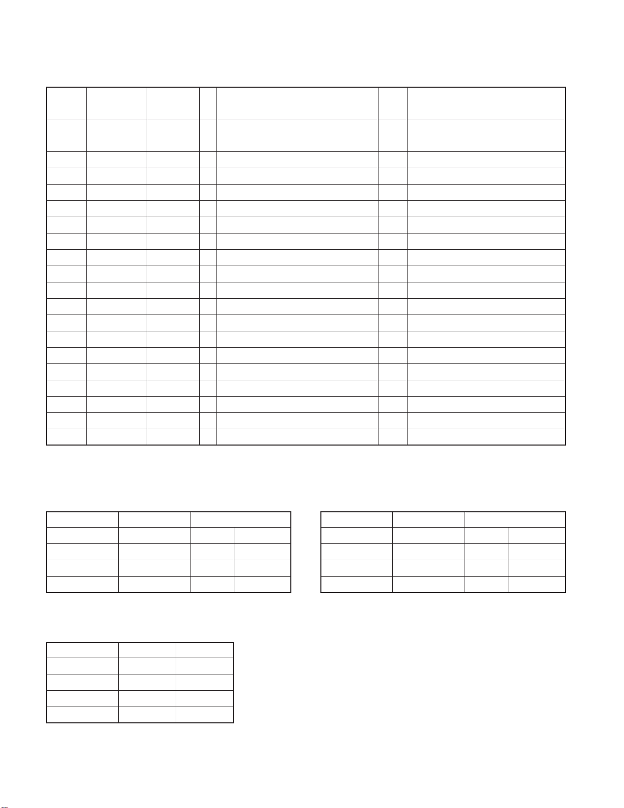
MICROCOMPUTER’S TERMINAL DESCRIPTION
Pin No. Pin Name
36
37 BE_RST B/E O B/E circuit reset L: RESET
38 POWER_DET
39 BL_DET INVERTER I Backlight abnormality detection H: Abnormality detection
40 B_PON
41,42 NC O
43 FSEL1
44 FSEL2
45 FSEL_SW
46 PON
47 MCNT
48 RGB_SW VIDEO O RGB signal switching L: DVD, H: OTHER
49 OSD_CS OSD O OSD-IC chip select (OSD)
50 OSD_DATA OSD O Data output to OSD-IC (OSD)
51 OSD_CLK OSD O Clock output to OSD-IC (OSD)
52 OSD_RST OSD O Resetting OSD-IC (OSD)
53 WRT_E2P µCOM I Used for E2P writing
54 POWER_PWM
55 JIG_EJ EXTRA I 2DIN
56 PWM INVERTER O Liquid crystal brightness control
57 STATUS0 JIG O For monitor mechanism endurance Jig
58 STATUS1 JIG O For monitor mechanism endurance Jig
59 PANEL_DET PANEL I Front panel attach/detach detection H: Detached, L: Attached 2DIN L-fixed
60 STATUS2 JIG O For monitor mechanism endurance Jig
61 SH_MDATA SH-3 O Data output to SH-3 µ-com (GRAPHIC)
62 SH_SDATA SH-3 I Data input from SH-3 µ-com (GRAPHIC) OSD is output
63,64 NC O
65 SYS_SREQ BOX I Request from BOX µ-com
66 SYS_MREQ BOX O Request to BOX µ-com
67 SYS_ON BOX O BOX µ-com ON/OFF control H: ON, L: OFF
68 SYS_SDATA BOX I Data input from BOX µ-com
69 SYS_MDATA BOX O Data output to BOX µ-com
70 SYS_CLK BOX O Communication clock with BOX µ-com 250kHz
71 MINI_CS/MINI_CS PANEL O Communication with mini liquid crystal
71
72
72
72
73
73
SCL/CHROMA_SCL
MINI_CS/FLASH_SDATA
MINI_MDATA/MINI_MDATA
MINI_MDATA/SUBLED_SW
MINI_MDATA/FLASH_MDATA
MINI_CLK/MINI_CLK
MINI_CLK/FLASH_CLK
Module (physical)
Chroma γ I/O Access with chroma γ IC
Power supply
Power supply
Power supply
Power supply
Power supply
Power supply
Power supply
Power supply
µCOM I For flash writing
PANEL O Communication with mini liquid crystal
PANEL O
µCOM O For flash writing
PANEL O Communication with mini liquid crystal
µCOM I For flash writing
I/O Application Processing Operation Description
I 8.5V over current detection H: Abnormality detection
O SW14 (BU SW)ON/OFF control H: ON
O DC-DC IC oscillation frequency switching
O DC-DC IC oscillation frequency switching
O Control at DC-DC IC FSEL switching Normal: H, At FSEL switching: L
OPower supply ON/OFF control H: ON
O
Motor driver voltage switching (MECHA7V) (1DIN)
O DC/DC-IC oscillation frequency control
Model without mini liquid crystal LED ON/OFF
H: 7V, L: 5V
PWM output.
At FSEL switching stopped. (Output L)
HI: ON
16

KVT-817DVD/827DVD/827DVDY
KVT-837DVD/847DVD/867DVD
MICROCOMPUTER’S TERMINAL DESCRIPTION
Pin No. Pin Name
74
74
75 SRC PANEL I Source key L: ON
76 EJECT PANEL I Eject key (1DIN) L: ON 2DIN HI-fixed input
77 MINI_PON PANEL O MINI liquid crystal Power supply control H: ON, L: OFF
78 DSI PANEL O DSI control (1DIN)
79 ILL_DET
80 PAK_DET
81 REV_DET
82~84 NC O
85 SH_INI SH-3 O (GRAPHIC)
86 SH_STBY SH-3 I (GRAPHIC)
87 SH_SREQ SH-3 I Request from SH-3 µ-com (GRAPHIC)
88 SH_MREQ SH-3 O Request to SH-3 µ-com (GRAPHIC)
89 SH_CON SH-3 O (GRAPHIC)
90 SH_RST SH-3 O SH-3 µ-com resetting (GRAPHIC)
91 TOUCH SH-3 I (GRAPHIC)
92 TOUCH_EN SH-3 O (GRAPHIC)
93 NAVI_L VIDEO O L: NAVI, H: OTHER
94~97 TYPE0~TYPE3 EXTRA I Destination setting Refer to destination setting
98 SUBLED_OFF Other X35 O 2DIN disc LED control (2DIN)
99 TMOTOR_M
99 TILT_UP
100 TMOTOR_P
100 TILT_DOWN
101 SMOTOR_M
102 SMOTOR_P
103 BVSS
104 BVDD
105 SW_A
106 SW_B
107 SW_C
108 SW_D
109 ENABLE INVERTER O Backlight ON/OFF control H: ON
110 FLMD1 µCOM I
111 Y0 Touch panel O Touch panel control (OSD)
112 X1 Touch panel O Touch panel control (OSD)
113 X0 Touch panel O Touch panel control (OSD)
114~117
118~120
121 MIRROR LCD O Rear monitor mirror control
OPEN_CLOSE/OPEN_CLOSE
OPEN_CLOSE/EJECT
HPOS1~HPOS4 LCD O Display position control
MODE1~MODE3 LCD O Aspect setting
Module (physical)
PANEL I OPEN_CLOSE key (1DIN) L: ON
PANEL I
Power supply
Power supply
Power supply
1DIN_MECHA
2DIN_MECHA
1DIN_MECHA
2DIN_MECHA
1DIN_MECHA
1DIN_MECHA
1DIN_MECHA
1DIN_MECHA
1DIN_MECHA
1DIN_MECHA
I/O Application Processing Operation Description
Tilt mechanism OPEN/CLOSE and eject (2DIN)
I ILLUMI detection H: Normal, L: Detect
IParking detection H: Normal, L: Detect
IReverse detection H: Normal, L: Detect
O Monitor mechanism tilt control (1DIN)
O Tilt mechanism control (2DIN)
O Monitor mechanism tilt control (1DIN)
O Tilt mechanism tilt control (2DIN)
O Monitor mechanism slide control (1DIN)
O Monitor mechanism slide control (1DIN)
I Monitor mechanism detection(1DIN) 2DIN is OUT
I (1DIN) 2DIN is OUT
I Monitor mechanism detection 2DIN is OUT
I Monitor mechanism detection 2DIN is OUT
L: ON
17

KVT-817DVD/827DVD/827DVDY
KVT-837DVD/847DVD/867DVD
MICROCOMPUTER’S TERMINAL DESCRIPTION
Pin No. Pin Name
122 ILL_R PANEL O Key ILLUMI red ON/OFF H: ON, L: OFF
123 ILL_G PANEL O Key ILLUMI green ON/OFF H: ON, L: OFF
124 ILL_B PANEL O Mini liquid crystal backlight blue ON/OFF H: ON, L: OFF
125 NTSC_PAL VIDEO O
126 LED_SW/SI Other X35 O
126 LED_SW/SI Other X35 O SI control (2DIN) H: Light turn ON, L: Light turned OFF
127 LCD_PON LCD O LCD power supply ON/OFF control H: ON
128~134
135 TL_DET
136 KEY1 PANEL I 4 key monitor mechanism section (1DIN)
137 KEY2 PANEL I 8 key attach/detach panel section (1DIN)
138 KEY3 PANEL I 6 key panel section (2DIN)
139 KEY4 PANEL I 6 key panel section (2DIN)
140 R_SENS
140 R_SENS
141 PH_DET
142 AUTO_DIM Other X35 I Auto dimmer input
143 YDATA Touch panel I Touch data input (OSD)
144 XDATA Touch panel I Touch data input (OSD)
NC O
Module (physical)
Power supply
1DIN_MECHA
2DIN_MECHA
1DIN_MECHA
I/O Application Processing Operation Description
LCD output signal NT/PAL identification output
LED blinking control at OPEN/CLOSE (1DIN)
I
Power supply reduced electric power detection
I Monitor mechanism tilt sensor (1DIN)
I Tilt mechanism tilt sensor (2DIN)
I Monitor mechanism slide detection (1DIN)
H: PAL, L: NTSC
H: Light turn ON, L: Light turned OFF
Destination setting of GRAPHIC model and OSD model
CLASSIFICATION CATEGORY MODEL NAME DESTINATION TYPE3 TYPE2 TYPE1 TYPE0
GRAPHIC 1DIN KVT-817DVD K 0 0 0 1
KVT-827DVD E 0 0 1 0
KVT-837DVD M 0 0 1 1
KVT-847DVD/867DVD V/X 0 1 0 0
2DIN DDX8017 K 1 0 0 1
DDX8027 E 1 0 1 0
DDX8037 M 1 0 1 1
DDX8047/8067 V/X 1 1 0 0
OSD 1DIN KVT-717DVD K 0 0 0 1
KVT-627DVD/727DVD E 0 0 1 0
KVT-737DVD M 0 0 1 1
KVT-747DVD/767DVD V/X 0 1 0 0
KVT-747DVD R 0 1 1 1
2DIN DDX7017 K 1 0 0 1
DDX6027 E 1 0 1 0
DDX7037 M 1 0 1 1
DDX7047/7067 V/X 1 1 0 0
DDX7047 R 1 1 1 1
18

KVT-817DVD/827DVD/827DVDY
KVT-837DVD/847DVD/867DVD
MICROCOMPUTER’S TERMINAL DESCRIPTION
● Graphic Microcomputer: 6417706F120DV (X14: IC800)
Pin No. Pin Name Module I/O Application Processing Operation Description
1 Vcc-RTC
2XTAL2 EXTRA O Built-in RTC crystal oscillator terminal NC
3 EXTAL2 EXTRA I Built-in RTC crystal oscillator terminal Pull-up to Vcc
4 Vss-RTC
5~10 D31~D26 EXTRA I/O Data bus
11 VssQ
12 D25 EXTRA I/O Data bus
13 VccQ
14~18 D24~D20 EXTRA I/O Data bus
19 Vss
20 D19 EXTRA I/O Data bus
21 Vcc
22~24 D18~D16 EXTRA I/O Data bus
25 VssQ
26 D15 EXTRA I/O Data bus
27 VccQ
28~36 D14~D6 EXTRA I/O Data bus
37 VssQ
38 D5 EXTRA I/O Data bus
39 VccQ
40~44 D4~D0 EXTRA I/O Data bus
45~48 A0~A3 EXTRA O Address bus
49 VssQ
50 A4 EXTRA O Address bus
51 VccQ
52~60 A5~A13 EXTRA O Address bus
61 VssQ
62 A14 EXTRA O Address bus
63 VccQ
64~70 A15~A21 EXTRA O Address bus
71 Vss
72 A22 EXTRA O Address bus
73 Vcc
74~76 A23~A25 EXTRA O Address bus
77 BS EXTRA O Bus cycle start signal
78 RD EXTRA O Lead strobe
79 WE0/DQMLL EXTRA O D7~D0 select signal /DQM (SDRAM)
80 WE1/DQMLU EXTRA O D15~D8 select signal /DQM (SDRAM)
81 WE2/DQMUL EXTRA O D23~D16 select signal /DQM (SDRAM)
Power supply
Power supply
Power supply
Power supply
Power supply
Power supply
Power supply
Power supply
Power supply
Power supply
Power supply
Power supply
Power supply
Power supply
Power supply
Power supply
-RTC power supply 1.9V
-
-
- I/O power supply 3.3V
-
- Internal power supply 1.9V
-
- I/O power supply 3.3V
-
- I/O power supply 3.3V
-
- I/O power supply 3.3V
-
- I/O power supply 3.3V
-
- Internal power supply 1.9V
19

KVT-817DVD/827DVD/827DVDY
KVT-837DVD/847DVD/867DVD
MICROCOMPUTER’S TERMINAL DESCRIPTION
Pin No. Pin Name Module I/O Application Processing Operation Description
82 WE3/DQMUU EXTRA O D31~D24 select signal /DQM (SDRAM)
83 RDWR EXTRA O Read/Write
84 VssQ
85 CS0 EXTRA O Chip select 0 (ROM) For ROM
86 VccQ
87 CS2 EXTRA O Chip select 2 (For DMA)
88 CS3 EXTRA O Chip select 3 (SDRAM) For SDRAM
89 CS4 EXTRA O Chip select 4 (SRAM) For SRAM
90 CS5 EXTRA O Chip select 5 (GRiTT: VRAM) For GRITT
91 CS6 EXTRA O Chip select 6 (GRiTT: Register) For GRITT
92 NC O
93 VssQ
94 NC O
95 VccQ
96 RAS EXTRA O Row address strobe
97 NC O NC
98 CAS EXTRA O Colum address strobe
99 NC O
100 CKE EXTRA O Clock enable
101 SHINI V850 I Resetting start identification H: Other than reset start, L: Reset start
102 BACK EXTRA O Bus acknowledge NC
103 BREQ EXTRA I Bus right request High level fixed.
104 R_WAIT GRITT I Hardware wait request
105 SH_DACK GRITT O DMA acknowledge
106,107
108 SHSTBY V850 O Power supply OFF permission
109 AUDATA0 H-UDI I/O AUDATA input/output
110 AUDATA1 H-UDI I/O AUDATA input/output
111 AUDATA2 H-UDI I/O AUDATA input/output
112 AUDATA3 H-UDI I/O AUDATA input/output
113 AUDSYN.C H-UDI O AUDSYNC output (H-UDI)
114 TDI H-UDI I Data input (H-UDI)
115 Vss
116 TCK H-UDI I Clock (H-UDI)
117 Vcc
118 TMS H-UDI I Mode select (H-UDI)
119 TRST H-UDI I Reset (H-UDI)
120 TDO H-UDI O Data output (H-UDI)
121 ASEBRKAK H-UDI O ASE break acknowledge (H-UDI)
NC O
Power supply
Power supply
Power supply
Power supply
Power supply
Power supply
-
- I/O power supply 3.3V
-
- I/O power supply 3.3V
H: Power supply OFF not permitted
L: Power supply OFF permitted
-
- Internal power supply 1.9V
20

KVT-817DVD/827DVD/827DVDY
KVT-837DVD/847DVD/867DVD
MICROCOMPUTER’S TERMINAL DESCRIPTION
Pin No. Pin Name Module I/O Application Processing Operation Description
122 ASEMD0 H-UDI I ASE mode (H-UDI)
123 Vcc-PLL1
124 CAP1
125 Vss-PLL1
126 Vss-PLL2
127 CAP2
128 Vcc-PLL2
129 MD1 EXTRA I Clock mode setting
130 Vss
131 XTAL EXTRA O Crystal oscillator terminal NC
132 EXTAL EXTRA I
133 NC O
134 SH_SREQ V850 O
135 SH_MREQ V850 I
136 NC O
137 VssQ
138 CKIO EXTRA O System clock output
139 VccQ
140,141
142 SH_SDATA V850 UART
143 NC O
144,145
146 SH_MDATA V850 UART
147 R_INT GRITT I Interruption request from graphic IC
148 Vss
149 RESETM EXTRA I Manual resetting request High level fixed
150 Vcc
151 TOUCH V850 O Touch off detection H: Touch OFF, L: Touch ON
152 TOUCH_EN V850 I Touch control enable
153 X1 X35 O Touch panel control
154 X0 X35 O Touch panel control
155 SHCON V850 I Graphic µ-com operation control H: Operation possible, L: Operation not possible
156 VssQ
157 NMI EXTRA I Non-maskable interruption Low level fixed
158 VccQ
159 AUDCK H-UDI I AUDCK input (H-UDI)
160 R_DREQ GRITT I DMA request
161 Y0 X35 O Touch panel control
162 NC I Low level fixed
163 MD0 EXTRA I Clock mode setting High level fixed
NC O
NC I
Power supply
Power supply
Power supply
Power supply
Power supply
Power supply
Power supply
Power supply
Power supply
Power supply
Power supply
Power supply
Power supply
- PLL1 power supply 1.9V
- PLL1 external capacity terminal 470pF
-
-
- PLL2 external capacity terminal 470pF
- PLL2 power supply 1.9V
-
External clock input / Crystal oscillator terminal
-
- I/O power supply 3.3V
-
- Internal power supply 1.9V
H: Touch control possible, L: Touch control not possible
-
- I/O power supply 3.3V
21

KVT-817DVD/827DVD/827DVDY
KVT-837DVD/847DVD/867DVD
MICROCOMPUTER’S TERMINAL DESCRIPTION
Pin No. Pin Name Module I/O Application Processing Operation Description
164 MD2 EXTRA I Clock mode setting Low level fixed
165 SH_RST V850 I
166 CA EXTRA I Hardware standby request High level fixed
167 MD3 EXTRA I CS0 space bus width designation Low level fixed
168 MD4 EXTRA I CS0 space bus width designation High level fixed
169 MD5 EXTRA I Endean setting Low level fixed
170 Avss
171 XDATA X35 I Touch panel input (X-direction)
172 YDATA X35 I Touch panel input (Y-direction)
173,174
175 Avcc
176 AVss
NC O
Power supply
Power supply
Power supply
-
-Power supply for analog 3.3V
-
● Audio Microcomputer: 703068YGJ128A (X34: IC303)
Pin No. Pin Name
1 DC_ERR IC2
2 LINE_MUTE DC-CN I LINE MUTE detection
3,4 NC NC I
5 PORTGND0 µCOM
6
7
8
9
10,11 NC O
12~14 NC NC O
15 NC O L: MUTE ON, H: MUTE OFF
16 NC O
17 NC NC O
18
19
20 MUTE_PRE MUTE O MUTE for PREOUT L: MUTE ON, H: Normal
AUDIO_SW1_A
AUDIO_SW1_B
AUDIO_SW2_A
AUDIO_SW2_B
EEPROM_WRT
MUTE_AVOUT
Module
(physical) Table
VI
Audio O
Audio O
Audio O
Audio O
EEPROM I Write detection at ROM correction
MUTE O MUTE for AVOUT L: MUTE ON, H: Normal
I/O Application
I DC offset detection Low at the detection
LX/NAVI1/SW3 (or TV) /
AVIN1 audio switching (For main)
LX/NAVI1/SW3 (or TV) /
AVIN1 audio switching (For main)
TV/AVIN1/AVIN2 audio switching (For sub)
TV/AVIN1/AVIN2 audio switching (For sub)
Truth Value
Processing Operation Description
Normal: 1.6V, TEL MUTE: 1V or lower,
NAVI MUTE: 2.5V or higher
q Refer to truth value table
q Refer to truth value table
w Refer to truth value table
w Refer to truth value table
When writing to E2PROM from outside,
Hi is input with a jig. (Common use SCL
and SDA will stop operation)
In other cases: Low (Pull-down)
22

KVT-817DVD/827DVD/827DVDY
KVT-837DVD/847DVD/867DVD
MICROCOMPUTER’S TERMINAL DESCRIPTION
Pin No. Pin Name
21 P_CON DC-CN O External amp power supply control On during STANDBY),
22 PORTVDD0 µCOM
23 EXT_CONT DC-CN O External amp control
24 ANT_CONT DC-CN O Power antenna control H: Antenna UP,
25 P_ON
26 PWIC_MUTE POWER-IC O POWER-IC MUTE control
27 PWIC_STBY POWER-IC O POWER-IC standby control H: POWER ON, L: POWER OFF
28 NC O
29
29 AUD_SDA IC2
30
30 AUD_SCL IC2
31 MUTE0 IC2
32 MUTE1 IC2
33 MUTE2 IC2
34 NAVI_FLAG IC2
35 MUTEC IC2
36 NC NC O
37 GND0 µCOM
38 CPUREG µCOM
39 VDD0 µCOM
40 RESET µCOM
41 MODE/VPP µCOM
42 FLASH_SI FLASH I Data input at flash write
42 SYS_MDATA to X14 I Data from system control µ-com
43 FLASH_SO FLASH O Data output at flash writing
43 SYS_SDATA to X14 O Data to system control µ-com
44 FLASH_CLK FLASH I CLK input at the flash writing
44 SYS_MCLK to X14 I Clock from system control µ-com
45 BU_DET DC-CN I Backup reduced electric power detection
46 DIR_CDTO
47 DIR_CDTI
EEPROM_SDA
EEPROM_SCL
Module
(physical) Table
Power supply
EEPROM I/O Data for EEPROM (ROM correction)
VI
EEPROM I/O Clock for EEPROM (ROM correction)
VI
VI
VI
VI
VI
VI
DSP BLOCK
DSP BLOCK
I/O Application
O
SW5V→SW14V power supply ON/OFF control
I/O Data for IC2
I/O Clock for IC2
O MUTE for IC2 VI OUT0 L: MUTE ON, H: MUTE OFF
O MUTE for IC2 VI OUT1 L: MUTE ON, H: MUTE OFF
O MUTE for IC2 VI OUT2 L: MUTE ON, H: MUTE OFF
Monitoring whether NAVI interruption is L: No NAVI interruption
O
taking place H: NAVI interruption in progress
O MUTE for IC2 VI MUXC L: MUTE ON, H: MUTE OFF
I Input data for DIR
O Output data for DIR
VI
VI
Truth Value
Processing Operation Description
Hi: During POWER ON (Does not come
Low: During STANDBY or POWER OFF
Hi at FMAM selection→Antenna UP
In other cases Low→Antenna DOWN
H: ON, L: Normal
L: MUTE ON (At POWER, ACC OFF,
STANDBY, momentary power down)
Low when 8.8V or higher. Hi when
reduced electric power (8.8V or lower)
23

KVT-817DVD/827DVD/827DVDY
KVT-837DVD/847DVD/867DVD
MICROCOMPUTER’S TERMINAL DESCRIPTION
Pin No. Pin Name
48 DIR_CCLK
49,50 NC NC O
51 ADC_RST
52 DIR_RST
53 DAC_RST
54 DSP_RST
55 DIR_CS
56 DAC_CS
57 DIR_ERRF
58 DSP_SS
59 ADC_MUTE
60 PORT/VDD1 µCOM
61 DAC_MUTE
62~64 NC NC O
65 BM_SW
66 DSP_INFO
67,68 NC NC O
69 SYS_ON to X14 I
70,71 XT2, XT1 µCOM
72 GND2 µCOM
73,74 X1, X2 µCOM
75,76 NC NC
77 LX_RST LX_M O Hard to resetting to slave unit H: Reset, L: Normal
78 LX_MUTE LX_M I Muting request from slave unit H: Mute ON, L: Mute OFF
79 LX_REQ_M LX_M O Communication request to slave unit
80 LX_CON LX_M O Startup requests to slave unit H: Slave unit ON, L: Slave unit OFF
81 LX_REQ_S LX_M I Communication request from slave unit
82 NC NC O
83 TV_SREQ TV I Request from TV unit
84 TUN_SDA FST I/O F/E I2C data input/output terminal
85 NC NC O
86 TUN_SCL FST I/O F/E I2C clock output terminal (MAX 400kHz)
87,88 NC NC O
89 PWIC_BEEP POWER-IC O Beep output
90 SYS_MREQ to X14 I Request from system control µ-com
91 SYS_SREQ to X14 O Request to system control µ-com
92 PORTGND1 µCOM
93 DAC_CLK
93 DSP_SCL
Module
(physical) Table
DSP BLOCK
DSP BLOCK
DSP BLOCK
DSP BLOCK
DSP BLOCK
DSP BLOCK
DSP BLOCK
DSP BLOCK
DSP BLOCK
DSP BLOCK
DSP BLOCK
DSP BLOCK
DSP BLOCK
DSP BLOCK
DSP BLOCK
I/O Application
O Data clock for DIR
O Resetting for AD L: Reset
O Resetting for DIR L: Reset
O Resetting for DAC L: Reset
O Resetting for DSP L: Reset
O Chip select for DIR L: Select
O Chip select for DAC L: Select
I S/PDIF Unlock H: Error, L: No Error
O Select for DSP L: Select
O MUTE for AD L: MUTE ON, H: MUTE OFF
O MUTE for DAC L: MUTE ON, H: MUTE OFF
O Bus management SW H: BM ON, L: BM OFF
I
ON/OFF control from system control µ-com
O Communication clock for DAC
O Communication clock for DSP
Truth Value
Processing Operation Description
H: Box unit ON, L: Box unit OFF
24
KVT-817DVD/827DVD/827DVDY
KVT-837DVD/847DVD/867DVD
MICROCOMPUTER’S TERMINAL DESCRIPTION
Pin No. Pin Name
94 DAC_DO
94 DSP_SO
95 DAC_DI
95 DSP_SI
96 FSEL_1
97 FSEL_2
98 NC NC O
99 VSYNC_SW2 Visual O Switching for monitoring whether there is !4
100 TYPE4 TYPE I u Refer to truth value table
101 TV_CON TV O Start up request to TV unit H: TV unit ON, L: TV unit OFF
102 PORTVDD2 µCOM
103 TV_CLK TV O Clock to TV unit
104 TV_MREQ TV O Request to TV unit
105 TV_MDATA TV O Data to TV unit
106 TV_SDATA TV I Data from TV unit
107 LX_DATA_S LX_M I Data from slave unit
108 LX_DATA_M LX_M O Data to slave unit
109 LX_CLK LX_M I/O LX BUS clock
110
111 NAVI1_RX NAVI I Data from navigation 1
112 NAVI1_TX NAVI O Data to navigation 1
113 VISUAL_SW4 Visual O TV/Rear view camera video switching !2 Refer to truth value table
114 RGB_SW Visual O TV/NAVI1/NAVI2 RGB video switching !0 Refer to truth value table
115 TV_JUDGE TV I TV tuner old/new identification H: Old, L: New
116 VSYNC_SW1 Visual O Switching for monitoring whether there is !4
117,118 NC O
119
120 VSYNC_DET Visual I
121
122
123
124
125 RDS_CLK RDS I RDS decoder CLK input
VISUAL_SW5_1
VISUAL_SW3_2
VISUAL_SW3_1
VISUAL_SW2_2
VISUAL_SW2_1
VISUAL_SW1_2
Module
(physical) Table
DSP BLOCK
DSP BLOCK
DSP BLOCK
DSP BLOCK
DSP BLOCK
DSP BLOCK
Visual O TV/AVIN1 video switching !3 Refer to truth value table
Visual O NAVI1/NAVI2/AVIN2 video switching !1 Refer to truth value table
Visual O NAVI1/NAVI2/AVIN1 video switching !1 Refer to truth value table
Visual O SW5 (or TV)/AVIN2/DVD video switching o Refer to truth value table
Visual O SW5 (or TV)/AVIN2/DVD video switching o Refer to truth value table
Visual O
I/O Application
ICommunication data for DAC
I Communication data for DSP
OCommunication data for DAC
O Communication data for DSP
OFrequency selection for DC/DC
OFrequency selection for DC/DC
NTSC/PAL identification COMP signal
AUTO detection COMP signal or not
NTSC/PAL identification COMP signal
AUTO detection COMP signal or not
Vertical synchronization signal detection
(For AVIN2 automatic detection)
AVIN2/SW5 (or TV)/
SW3 (or NAVI1) video switching
Truth Value
i Refer to truth value table
Processing Operation Description
25
KVT-817DVD/827DVD/827DVDY
KVT-837DVD/847DVD/867DVD
MICROCOMPUTER’S TERMINAL DESCRIPTION
Pin No. Pin Name
126
127
128 VDD1 µCOM
129 RDS_DATA RDS I RDS decoder DATA input
130 RDS_QUAL RDS I RDS decoder QUAL input SW5 (or TV)/AVIN1/DVD video switching
131 GND1 µCOM
132 P_ON_AM FST O AM power supply ON/OFF control H: ON (AM selected), L: Normal
133 RDS_AFS FST I/O Constant switching at noise detection
134 TYPE3 TYPE I Destination setting u Refer to truth value table
135 RDS_NOISE FST I FM noise detection
136
137
138 TYPE0 OEM I Destination setting u Refer to truth value table
139 TYPE1 OEM I Destination setting u Refer to truth value table
140 TYPE2 Type I Destination setting u Refer to truth value table
141 OEM_TYPE0 Type I OEM destination setting y Refer to truth value table
142 OEM_TYPE1 Type I OEM destination setting y Refer to truth value table
143 ADCVDD µCOM
144 ADCGND µCOM
VISUAL_SW1_1
VISUAL_SW5_2
TUN_SMETER
TUN_IFC_OUT
Module
(physical) Table
Visual O
Visual O TV/AVIN1 video switching !3 Refer to truth value table
FST I S-meter input
FST I F/E IFC OUT input terminal H: With station, L: Without station
I/O Application
AVIN2/SW5 (or TV)/
SW3 (or NAVI1) video switching
Truth Value
i Refer to truth value table
Processing Operation Description
q Audio Selector 1 (TC4052BFT)
AUDIO_SW1_A AUDIO_SW1_B Output
LLIN3 AVIN1
HLIN2 TV
LHIN1 AVIN2
HHIN0 LX
∗ Input is reversed by transistor before entering selector.
y Destination setting for OEM
Destination TYPE0 TYPE1
Marketing 0 0
OEM1 0 1
OEM2 1 0
EU Installation 1 1
26
w Audio Selector 2 (TC4052BFT)
AUDIO_SW2_A AUDIO_SW2_B Output
LLIN3 AVIN2
HLIN2 AVIN1
LHIN1 TV
HHIN0 Not used
∗ Input is reversed b y transistor before entering selector.
KVT-817DVD/827DVD/827DVDY
KVT-837DVD/847DVD/867DVD
MICROCOMPUTER’S TERMINAL DESCRIPTION
u TYPE4, TYPE3, TYPE2, TYPE1, TYPE0
Category Model Destination TYPE4 TYPE3 TYPE2 TYPE1 TYPE0
1DIN KVT-817DVD K Reserve 0 0 0 1
KVT-827DVD E Reserve 0 0 1 0
KVT-837DVD M Reserve 0 0 1 1
KVT-867DVD V Reserve 0 1 0 0
KVT-847DVD X Reserve 0 1 0 1
KVT-727DVD E2 Reserve 0 1 1 0
KVT-747DVD R Reserve 0 1 1 1
2DIN DDX8017 K Reserve 1 0 0 1
DDX8027 E Reserve 1 0 1 0
DDX8037 M Reserve 1 0 1 1
DDX8067 V Reserve 1 1 0 0
DDX8047 X Reserve 1 1 0 1
∗ Reserve terminal is pulled down.
i Video Selector 1 (MM1228XFBE)
VISUAL_SW1_1 VISUAL_SW1_2 Output
LLIN1 AVIN1
HLIN2 SW4
L/H H IN3
o Video Selector 2 (MM1228XFBE)
VISUAL_SW2_1 VISUAL_SW2_2 Output
LLIN1 AVIN1
HLIN2 SW5 (or TV)
L/H H IN3 DVD
!0 RGB_SW (MM1503 or MM1508)
RGB_SW Output
L IN1 NAVI
H IN2 TV
!1 Video Selector 3 (BA7652AF)
VISUAL_SW3_1 VISUAL_SW3_2 Output
LLIN1 NAVI
HLIN2 AVIN2
LHIN3 Not used
HHMUTE -
!2 Video Selector 4 (MM1503)
VISUAL_SW4 Output
L IN1 TV
H IN2 Rear view
SW3 (or NAVI)
!3 Video Selector 5 (BA7652AF)
VISUAL_SW5_1 VISUAL_SW5_2 Output
LLIN1 TV
HLIN2 AVIN2
LHIN3 Not used
HHMUTE -
!4 VSYNC Selector (BA7652AF)
VSYNC_SW1 VSYNC_SW2 Output
LLIN1 AVIN2
HLIN2 CAMERA
LHIN3 AVIN1
HHMUTE -
About muting of composite signal to X14
• Video Selector 1 is set to SW3 and Video Selector 3 is set
to MUTE. Mute timing is at full OSD.
27

KVT-817DVD/827DVD/827DVDY
KVT-837DVD/847DVD/867DVD
MICROCOMPUTER’S TERMINAL DESCRIPTION
● Disc Controller Microcomputer: MN103S71F (X37: IC4)
Pin No. Pin Name I/O Application
1 SW_2 I
2 SW_3 I Lo-START detection
3 CDON O CD-LD ON
4 VDD3 - VDD (3.3V)
5 VSS - VSS
6FGIMotor FG input
7 SW_4 I Lo-END detection
8,9 FADR17,18 O Address output to FLASH
10 FADR11 O Address output to FLASH
11 FADR9 O Address output to FLASH
12 VDD15 - VDD (1.5V)
13 FADR8 O Address output to FLASH
14,15 FADR13,14 O Address output to FLASH
16 NWE O Right signal output to FLASH
17,18 FADR16,15 O Address output to FLASH
19 DRAMVDD15 - DRAM power supply (1.5V)
20 DRAMVSS - VSS for DRAM
21 VSS - VSS
22 FADR12 O Address output to FLASH
23~30 FADR7~0 O Address output to FLASH
31 VSS - VSS
32 VDD3 - VDD (3.3V)
33~40 FDT0~7 I/O Data input/output with FLASH
41 NCE O
42 FADR10 O Address output to FLASH
43 NOE O Read signal output to FLASH
44 MMOD I Test mode switching signal
45 NRST I Reset input
46 VSS - VSS
47 SCLOCK I/O Dwire clock terminal
48 SDATA I/O Dwire data terminal
49 TxD/EXTRG0 I/O
50 RxD/EXTRG1 I/O
51 VDD3 - VDD (3.3V)
52 OSCI I
53 OSCO O
54 VSS - VSS
8cm Ej-STOP, Lo-START detection
Chip select signal output to FLASH
Serial transmission/
Dwire trigger terminal
Serial reception/
Dwire trigger terminal
Oscillation input (16.897849MHz)
Oscillation output (16.897849MHz)
Pin No. Pin Name I/O Application
55 OFS_TE O CD TE offset cancel output
56 DRV1 O Drive output for spindle drive
57 DRV2 O
58 DVDON O DVD-LD ON
59 STEP_A O Thread control output A
60 STEP_B O Thread control output B
61 Lo/Ej O Lo/Ej control terminal
62 LO.MUTE O Lo/Ej mute terminal
63 VSS - VSS
64 DRV.MUTE O Driver mute control
65 BMS O Spindle short brake control
66 LIM-SW I LIM-SW detection
67 Gain_SW O PDIC Gain switching
68 FEPCK O FEP clock output
69 FEPDT O FEP data output
70 FEPEN O FEP enable signal
71 DRAMVSS - VSS for DRAM
72 DRAMVDD15 - DRAM power supply (1.5V)
73 DRAMVDD33 - DRAM power supply (3.3V)
74 VDD3 - VDD (3.3V)
75 FG I Motor FG input
76 TX O Output for digital OUT
77 VDD15 - VDD (1.5V)
78 VSS - VSS
79 TSTSG O EQ calibration signal
80 VFOSHORT O Not used.
81 JLINE O J-line setting output
82 BDO I Dropout signal input
83 OFTR I Off-track signal input
84 AVSSD - VSS for analog
85 ROUT O MASH Rch audio output
86 LOUT O MASH Lch audio output
87 AVDDD - VDD (3.3V) for analog
88 VCOF I JFVCO control voltage
89 TRCRS I
90 AVDDC - VDD (3.3V) for analog
91 WBLIN I WBL input
92 CSLFLT I Not used
93 RFDIF I Not used
Focus balance adjustment output
Track loss generation signal input
28
KVT-817DVD/827DVD/827DVDY
KVT-837DVD/847DVD/867DVD
MICROCOMPUTER’S TERMINAL DESCRIPTION
Pin No. Pin Name I/O Application
94 AVSSC - VSS for analog
95 PLFLT2 I Condenser 2 for PLL
96 PLFLT1 I Condenser 1 for PLL
97 AVSSB - VSS for analog
98 ARF I Equivalent RF+ input
99 NARF I Equivalent RF- input
100 VHALF I Reference voltage 1.65V input
101 RV1 I
102 VREFH I Reference voltage 2.2V input
103 DSLF2 I Condenser 2 for DSL
104 DSLF1 I Condenser 1 for DSL
105 AVDDB - VDD (3.3V) for analog
106 JITOUT O For jitter monitor
107 AVDDA - VDD (3.3V) for analog
108 TECAPA I Not used
109 AD0 (FE) I FE input
110 AD2 (AS) I AS input
111 AD1 (TE) I TEph/TE3b input
112 AD3 (ENV) I RF envelop input
113
114 AD5 I Focus drive AD input
115 AD6 I Tracking drive AD input
116 AD7 (IOP) I
117
118 AVSSA - VSS for analog
119 PWM0 (FOD) O Focus drive output
120 PWM1 (TRD) O Tracking drive output
121 VSS - VSS
122 VDD3 - VDD (3.3V)
123 IDGT O Not used
124 DTRD O Not used
125 MONI0 O Internal monitor signal
126~130
131 SW_2∗3I
132 SW_1∗5I12cm Ej-STOP detection
133 DMARQ O DMA request output ATAPI host
134 NIOWR I ATAPI host write signal input
135 VDD3 - VDD (3.3V)
136 VSS - VSS
AD4 (RFDIFO)
AD8 (TEMP_DET)
MONI1~5 O Internal monitor signal
VREFH register for reference
current power supply
I Push-pull TE input
Laser diode current measurement
ITemperature monitoring input
8cm Ej-STOP, Lo-START detection
Pin No. Pin Name I/O Application
137 NIORD I ATAPI host read signal input
138 IORDY O Ready output to ATAPI host
139 NDMACK I
140 INTRQ O Interruption output to ATAPI host
141 NIOCS16 O Not used
142 DA1 I ATAPI host address signal input
143 NPDIAG I
144 DA0 I ATAPI host address signal input
145 VSS - VSS
146 VDD3 - VDD (3.3V)
147 DA2 I ATAPI host address signal input
148 NCS1FX I
149 NCS3FX I
150 NDASP O ATAPI drive active/slave
151 HDD15 I/O ATAPI data input/output
152 HDD0 I/O ATAPI data input/output
153 HDD14 I/O ATAPI data input/output
154 HDD1 I/O ATAPI data input/output
155 HDD13 I/O ATAPI data input/output
156 VDD3 - VDD (3.3V)
157 VDD15 - VDD (1.5V)
158 VSS - VSS
159 HDD2 I/O ATAPI data input/output
160 HDD12 I/O ATAPI data input/output
161 HDD3 I/O ATAPI data input/output
162 HDD11 I/O ATAPI data input/output
163 HDD4 I/O ATAPI data input/output
164 HDD10 I/O ATAPI data input/output
165 HDD5 I/O ATAPI data input/output
166 VSS - VSS
167 VDD3 - VDD (3.3V)
168 HDD9 I/O ATAPI data input/output
169 HDD6 I/O ATAPI data input/output
170 HDD8 I/O ATAPI data input/output
171 HDD7 I/O ATAPI data input/output
172 VDDH - 5V reference power supply
173 NRESET I ATAPI reset signal input
174 MASTER I ATAPI master/slave signal input
175 SCL O EEPROM clock output
176 SDA I/O EEPROM data input/output
ATAPI host DMA acknowledge input
Diagnosis from ATAPI slave to master
ATAPI host chip select signal input
ATAPI host chip select signal input
29

KVT-817DVD/827DVD/827DVDY
KVT-837DVD/847DVD/867DVD
TEST MODE
Operation Specifications
● Compatible Models for This Test Mode Specification
1Din GRA 1Din OSD 2Din GRA 2Din OSD M707
DSP Exist DSP Exist DSP None DSP Exist DSP None DSP None
K KVT-817DVD - KVT-717DVD DDX8017 DDX7017 KVT-M707
R- -KVT-747DVD - DDX7047 E KVT-827DVD KVT-727DVD KVT-627DVD DDX8027 DDX6027 KVT-M707
M KVT-837DVD - KVT-737DVD DDX8037 DDX7037 X KVT-847DVD - KVT-747DVD DDX8047 DDX7047 V KVT-867DVD - KVT-767DVD DDX8067 DDX7067 -
• Depending on Din/Display Types in the table below, test mode specifications may differ from model to model.
In this specification, categorizing by 1DIN/2DIN and Graphic/OSD, M707, DSP, and destinations (K/R/E/M/X/V).
Model Din Type DSP Display Type
KVT-8x7DVD 1DIN Exist Graphic
KVT-727DVD 1DIN Exist OSD
KVT-7x7/627DVD 1DIN None OSD
DDX80x7 2DIN Exist Graphic
DDX70x7/6027 2DIN None OSD
KVT-M707 1DIN None OSD
x: Different in accordance with the region code
● How to enter the test mode
There are two different ways to enter the test mode as shown
below.
1) While pressing [SRC key + ATT key] at the same time, reset
the unit.
2) Connect to Lx connector odd jigging for writing regions
(2DIN: When adjusting flicker)
Note1: The jig setting is arbitrary. Note that, how e ver, there
are functions according the setting SW. (Region/Serial/Security/CPPM)
Note2: In the test mode, power supply is cut off after 30
minutes. (This is for making the operation possible without
Security input even when the security is On.)
● Adjustment items
Items to be adjusted after writing on the EEPROM on which
regions have been written.
As for the details of the adjustments, ref er to each adjustment
item.
• Service Information/Serial Code writing
• Chroma adjustment
• Writing Touch Adjust values
• Screen position adjustment
• Writing Security Code (Other than K/R desinations)
30
● How to clear the Security Code
In adjusting K/R destination units, if the unit starts up with
Security ON, the Security Code can be cleared in the following manner. (Other than in Test Mode)
1)In the e Security ON condition, after resetting or turning
power ON after backup OFF, then the session star ts with
Security Code Input screen.
2)With the attached remote control in the Audio SW selected
condition, input the code with the following procedure.
Procedure 1: “K” input (Press Tenkey [5] 2 times)
Procedure 2: “C” input (Press Tenkey [2] 3 times)
Procedure 3: “A” input (Press Tenkey [2] once)
Procedure 4: “Q” input (Press Tenkey [7] 2 times)
Note: If a remote controller other than the attached is
used, Pressing Tenkey [7] twice will cause “R” to be input.
If a mistake is made during Procedure 1~4 above, input
other remote controller Key. Then, start inputting again
from Procedure 1.
3)Security Code is complete when the input screen for the
Security Code is cleared.
 Loading...