

Page 1
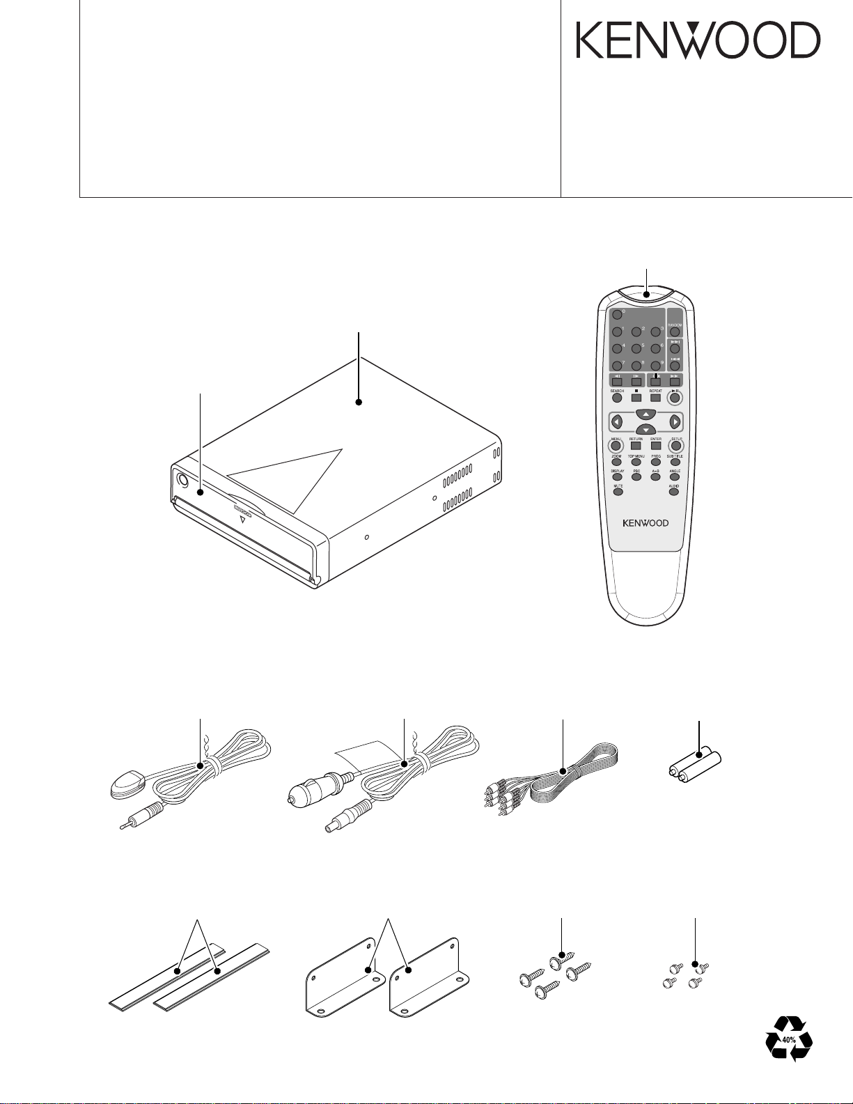
DVD PLAYER
KDV-S210P/S220P
/S230P/S240P
SERVICE MANUAL
Metallic cabinet
Panel assy
(A64-3526-08): KDV-S210P
(A64-3528-08): KDV-S220P
(A64-3529-08): KDV-S230P
(A64-3530-08): KDV-S240P
(A01-2845-08)
© 2004-5 PRINTED IN JAPAN
B53-0171-00 (N) 2703
Remote controller assy
(A70-2066-08)
Remote control sensor assy (6m)
(T95-0264-08)
Magic tape
(H30-0514-05)
x2
Cord with DC plug (2.4m)
(E03-0405-08)
Mounting hardware
(J22-0237-08)
x2
Cord with pinplug (3m)
(E30-6389-08)
Except KDV-S210P
Tapping screw
(N09-6274-08)
x4
RC-DV500
Size AAA battery
(Not supplied)
SEMS
(N09-6273-08)
x4
Page 2
2
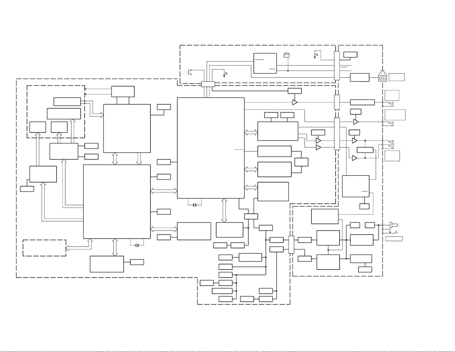
PROCESSOR
-DIGITAL SERVO CONTROL
DVD/CD DATA DECODING
SU6
SU1
SU3
MOTOR DRIVER
PWM
SU2
BTL
MOTOR DRIVER
HEAD AMPLIFIER
-GENERATING SERVO
-AUTO GAIN CONTROLLING
S+7V
MMVC
MVCC
DECODING & CORRECTING
-F/E CONTROL uP
-DATA BUFFERING
SVCC
-F/E PROGRAMING
FLASH MEMORY
3.3V
RFVCC
3.3V
VCC27
RFVCC
-DATA BUFFERING
DVD MPEG DECODING PROCESSOR
-MPEG DECODING
-B/E & SYSTEM CONTROL uP
U1
SU7
-B/E FRAME
SDRAM
-DVD/CD DATA
U34
CIRCUIT
LASER DRIVE
SQ4,5
U3
-F/E FRAME BUFFER
SDRAM 1Mx16BITS
-WORKING MEMORY
ACTUATOR &
BRUSHLESS
SY1
-F/E SYSTEM CLOCK
33.8688MHz
CERAMIC RESONATOR
CODE STORED
128kx8
-B/E SYSTEM CLOCK
CRYSTAL RESONATOR
27MHz
Y1
VCC27
-INCLUDING OVER
2ch AUDIO DAC
U35
DIGITAL FILTER
SAMPLING
U9
-RESETING
RESET IC
for U1
STORED
-SETUP & RESUME
EEPROM
INFORMATION
U2
U28
CODE STORED
-B/E PROGRAMING
FLASH ROM
VCC33
Q1
MMVC
MVCC
SVCC
3.3V
RFVCC
VCC33 AVCC
AVCC
RESET VCC
VCCA
S+7V
U5
REGULATOR
3.3V FIXED
SQ3
+7V
S7V
VCC
VCC
+7V
U23-1
U23-2
BUFFER
U27
POST LPF
-2nd ORDER
ACTIVE LPFx2
3.3V
CB5 CBP5
CBP7CB7
CB502 CBP502
CB3
CBD3
1MBITx8
BUFFER
4Mx16BITS
SERVO SIGNAL
RF AMPLITUDE
ERROR SIGNALS
INSERTION
DISC
SLIT
INDICATOR
EJECT SW
UD3
NAND GATES
POWER SW
INDICATOR
POWER
CBD1 CBP1
VCC
S7V
UP1
REGULATOR
SWITCHING
REGULATOR
SWITCHING
UP2
+B1
REGULATOR
5V
QP30
REGULATOR
QP40
28V
CIRCUIT
BU VCC
-GENERATING
TIMING
ON/OFF SW
DELAY CIRCUIT
VCC
RESET
REDUCING +B1
CIRCUIT
MUTE
-SENDING
DRIVING
-MUTE TR
+B1
ACTIVE LPFx2
LPF
-2nd ORDER
UP3-2
UP3-1
S7V
MUTE TR
QP4,5
UP4
VCC
75 Ohm
VIDEO
DRIVER
TRP1
PULSE TRANS
BU VCC
EYE INPUT
REMOTE
DC INPUT
ANALOG
OUT
AUDIO
VIDEO
OUT
COMPOSITE
DIGITAL
OUT
AUDIO
REMOTE
EYE
SPINDLE
MOTOR
to
SLEDGE
MOTOR
to
PICKUP HEAD
from SENSOR of
ACTUATOR COIL of
PICKUP HEAD
to
to CD LD
to DVD LD
+B
ERROR SIGNAL
INPUT
RF & SERVO
I/O
VPA
VM
PVCC
VCC
INTERFACE
COMMAND
DSP
CDLD DVDLD
DSP COMMAND
INTERFACE SIGNAL INPUT
RF & SERVO
CONTROL
LOADING
MECHANISM
OUTPUT
SERVO DRIVE SIGNAL
INTERFACE
FLUSH MEMORY
INTERFACE
SDRAM
AVDD5
INTERFACE
ATAPI
VDD 3.3
INTERFACE
SDRAM
INTERFACE
ATAPI
FLUSH MEMORY
EEPROM
RESET
DIGITAL AUDIO
VC25
INTERFACE
INTERFACE
INTERFACE
SPDIF OUT
SPDIF
UDAC
VIDEO DAC OUT
VC33
VCC
OUTPUT
SIGNAL
ERROR
RF & SERVO
RESET
HARDWARE
for F/E
INCLUDING
AUX4
AUX2
AUX7
VCC
VDD
VOUTR
VAA
VOUTL
VDD
ZRR
VCC
VCC
VCC
LED
RED
P DWN
P ON
+B DWN
LED
GREEN
IR
VSW
EN
VIN
VSW
EN
VIN
P ON
ZERO MUTE
VCC
V+ V+
CH-R
CH-L
VCC
+B DWN
P ON
IR
ZERO MUTE
SLOT-IN
LOADING MECHANISM
DISPLAY PCB POWER & OUTPUT PCB
COMBO PCB
TRAVERSE MECHANISM
KDV-S210P/S220P
/S230P/S240P
BLOCK DIAGRAM
Page 3
KDV-S210P/S220P
/S230P/S240P
COMPONENTS DESCRIPTION
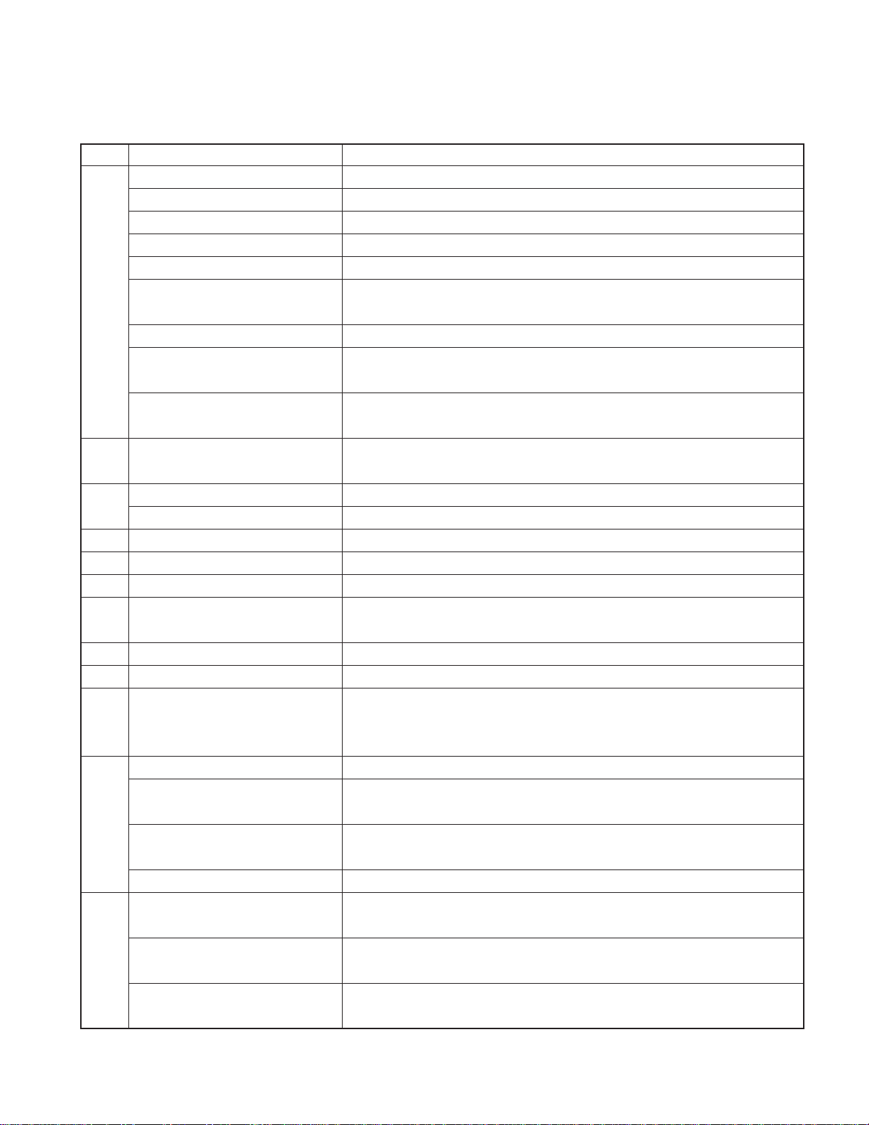
● COMBO PCB
Ref. No. Application / Function Operation / Condition / Compatibility
MPEG decoding control DVD MPEG images are decoded.
Dolby digital decoding control Outputs of Dolby digital audio are decoded.
LPCM audio decoding control LPCM audio of CD and DVD are decoded.
DVD navigation control DVD navigation is controlled.
ATAPI communication control ATAPI communication is control in order to control F/E.
U1
U2
U3
U5 3.3V regulator From No. 3 pin, VCC (5V) is input and from No. 2 pin, VCC33 (3.3V) is output.
U9 System reset control
U23 For audio post LPF CH1-side is Rch and CH2-side Lch. Constitutes a multiple feedback-type active LPF.
U27 SPDIF output, Pulse transformer driver
U28 B/E program memory Flash memory for storing B/E program memory.
U34 Program memory Flash memory for storing programs.
U35 Digital audio 2ch DAC
SU1
SU2 Feed motor driver
Built-in microcomputer for controlling
system and B/E system
Built-in video DAC Video DAC is built-in to output current for composite video output from No. 106 pin.
Digital audio DAC control output
Controls for keys and remote control
EEPROM for storing system setting
information and resume information
Frame buffer memory Decoding data buffer memory.
Program memory Memory for program control.
DVD/CD digital servo control Built-in DVD/CD digital servo equalizer and various timing generation circuit.
DVD/CD data decoding control
F/E section built-in system control
microcomputer
ATAPI communication control ATAPI communication control with B/E.
Pickup actuator driver
Motor driver for slot loading mechanism
System as a whole and B/E are controlled. 32bit RISC microcomputer is built-in.
Audio signals are output from No. 32 (TWS), 33 (TSD0), 39 (MCLK), and 40 (TBCK) pins. Also,
DAC system control is conducted using No. 160 (AUX0), 161 (AUX1), and 168 (AUX6) pins.
No. 162 pin is input for EJECT key. When receiving input, it is in L. No. 166 pin is for
remote control input. When receiving input, there will be pulse input.
EEPROM for storing system setting information and resume information.
Rising/Falling of VCC (5V) is detected by No. 5 pin, and L-reset output is made from No. 4 pin.
Inverters are connected in 3-step parallel connection for increased current capacity and
output to the pulse transformer.
Digital audio signal is input from No. 3 (TWS), 2 (TSD0), 16 (MCLK), and 1 (TBCK) pins.
Also, signals for DAC system control are input from No. 15 (AUX0), 14 (AUX1), and 13 (AUX6) pins.
Output for Lch analog audio is made from No. 7 pin and that for Rch is made from No. 8 pin.
Data generation from RF of DVD/CD, error correction and control over scramble analysis
and release.
F/E section 8bit microcomputer for system control.
Control signals for focus and tracking actuator signals of the pickup are received by No. 1 and
No. 26 pins respectively and currents are output from No. 13 and14 and No. 15 and 16 pins.
Control signals for the feed motor is received at No.6 pin and currents are output from
No. 11 and 12 pins.
Control signals for slot loading mechanism motor is received at No. 23 pin and currents
are output from No. 18 and 17 pins.
3
Page 4
KDV-S210P/S220P
/S230P/S240P
COMPONENTS DESCRIPTION
Ref. No. Application / Function Operation / Condition / Compatibility
SU3
SU6 amplifier control
SU7
SU8
SQ3 3.3V regulator VCC (5V) is input from No. 3 pin and 3.3V is output from No. 2 pin.
SQ4 Driver for LD-driving for CD
SQ5 Driver for LD-driving for DVD
Spindle motor driver
Spindle motor rotation detection Rotation FG output for controlling spindle motor is output from No. 27 pin.
DVD/CD servo error signal replay
Built-in DVD/CD laser APC circuit Built-in LD current control circuit for DVD/CD.
Frame buffer memory Memory for temporarily caching read data of DVD/CD.
System memory External microcomputer memory for F/E system control.
CH1-side CH1-side
Servo reference voltage generation Signal after dividing VC25 (2.5V) into 2.1V enters the positive phase and output from the
amplifier output terminal as buffer output.
CH2-side CH2-side
RFRP (mirror detection signal) RF bottom hold signal and its DC are input to reverse input and positive input respectively
generation amplifier for canceling DC fluctuation. These then can be used as mirror signals.
Timing is controlled by No. 18 pin control signal for the 3-phase brushless spindle motor, using
No. 1~6 pins Hall element input signals, while current outputs are made from No 20, 22 and 24 pins.
Generation of various servo signals from pick up signals.
CD’s LD current control signals output from SU6 are received at base and the current
amount for LD driving is controlled.
DVD’s LD current control signals output from SU6 are received at base and the current
amount for LD driving is controlled.
● THERMISTER PCB
Ref. No. Application / Function Operation / Condition / Compatibility
UT1 Inverter
UT2 Comparator
QT1 Switching TR
THT1
Temperature detection thermister for
thermal shutdown
Output from UT2 comparator is inverted. Input is made on No. 2 pin and output on No. 4
pin. Activ e L.
Signal from thermister is inverse input and reference voltage is input to positive-phase
input. Output from thermister is comparated and output from No . 4 pin. Active H.
UT1 output is received on the base and output is inverted when it is made. The output is
feedback into the positive-phase input at UT2 for containing the fluctuations in outputs.
Resistance value is low at low temperature and high at high temper ature.
● DISPLAY PCB
Ref. No. Application / Function Operation / Condition / Compatibility
UD3
Power supply ON/OFF delay circuit With +B_DWN of reduced voltage detection circuit and OR of /P_ON signal, /P_DWN
NOR gate IC signal is generated.
● POWER & OUTPUT PCB
Ref. No. Application / Function Operation / Condition / Compatibility
UP1
VCC (+5V) generation switching Power supply is input from No. 2 pin and switching output is made from No. 3 pin.
regulator IC Going via choke coil, it becomes VCC (+5V) power supply output.
4
Page 5

KDV-S210P/S220P
/S230P/S240P
COMPONENTS DESCRIPTION
Ref. No. Application / Function Operation / Condition / Compatibility
UP2 S7V generation switching regulator IC
UP3 Analog audio output LPF amplifier CH1-side is Rch and CH2-side is Lch. Constitutes non-inverse active LPF composition.
UP4
QP1 Mute circuit driving TR
QP2 Mute circuit switching TR When this TR comes ON, muting is ON and when it comes OFF, muting is OFF.
QP3 Mute circuit switching TR
QP4 Rch mute TR When base is H, Rch is muted.
QP5 Lch mute TR When base is H, Lch is muted.
QP8 Composite video output buffer driver TR When the input signal comes in on the base, output is made from the emitter.
QP9
QP10 Mute circuit switching TR
QP11 Mute circuit switching TR
QP12
QP15
QP20
QP21
QP22
QP30 BU_VCC (+5V) regulator driving TR
QP40 28V regulator drive TR
QP41
Composite video output 75Ω driver
amplifier IC
Power supply ON/OFF delay circuit SW TR
Power supply ON/OFF delay circuit SW TR
Reduced voltage detection switching
TR for resume operation
Power supply ON/OFF delay circuit SW TR
Power supply ON/OFF delay circuit SW TR
Power supply ON/OFF delay circuit SW TR
TR for comprising Darlington connection
Power supply is input from No. 2 pin and switching output is made from No. 3 pin.
Going via choke coil, it becomes S7V power supply output.
Input is made on No. 3 pin and output is made from No 6 pin.
When QP2 is ON, input is made to the emitter. Mute circuit driving power supply is output
from the collector.
This is a TR for switching QP2. Therefore, the logic is inverted and when the TR comes
ON, muting is OFF, and when the TR comes OFF, the muting is ON.
When this TR is ON, base current of QP21 is shut off. QP21 is OFF and switching power
supply is ON.
When Z_MUTE signal in the base of this TR is active, (H on no signal), QP1 is turned ON
and the mute circuit is driven.
/P_ON in the base becomes L when the power switch comes ON. Therefore, it is H when
the power is OFF. When this happens, QP3 is forced to go OFF and muting is driven.
On the base of this TR, power switch triggered /P_ON signal comes in. When this is L, and QP22
is turned ON, base current of QP20 is shut off. When QP20 is OFF, switching power supply is ON.
At the time of reduced +B1, base current is shut off and the circuit goes OFF.
When this TR is ON, switching power supply is OFF.
When this TR is ON, switching power supply is OFF.
When this TR is ON, base current at QP20 is shut off. This means QP20 is OFF and
switching power supply is ON.
Receives batter power supply (+B1) by the collector and outputs regulation voltage 28V
(+B1) from the emitter.
Receives battery current (+B) with collector and outputs regulated voltage 28V (+B1) from the
emitter. This is used to counter the surge current, and it is normally about +B- +B1 =1.4V.
Along with QP40, constitutes Darlington connection and works to enhance compound hfe.
5
Page 6

KDV-S210P/S220P
/S230P/S240P
MICROCOMPUTER’S TERMINAL DESCRIPTION
● B/E Microcomputer : ES6008 (COMBO PCB : U1)
Pin No. Pin Name I/O Application Processing Operation Description
1 VEE - I/O power supply (+3.3V) input
2~7 LA4~LA9 O Flash ROM address bus
8 VSS - Digital GND
9 VCC - Core power supply (+2.5V) input
10~16 LA10~LA16 O Flash ROM address bus
17 VSS - Digital GND
18 VEE - I/O power supply (+3.3V) input
19~21 LA17~LA19 O Flash ROM address bus
22,23 LA20,LA21 O Flash ROM address bus NC
24 /RESET I Chip reset input
25 TDMDX O NC
25 RSEL I ROM selection terminal Selected by 8bit ROM
26 VSS - Digital GND
27 VEE - I/O power supply (+3.3V) input
28 TDMDR I NC
29 TDMCLK I NC
30 TDMSF I NC
31 TDMTSC# O NC
32 TWS O Audio frame synchronization output
32 SEL_PLL2 I System and DSCK output clock selection [2] Selected by DCLK x 4
33 TSD0 O Audio serial data port 0
33 SEL_PLL0 I System and DSCK output clock selection [0] Selected by DCLK x 4
34 VSS - Digital GND
35 VCC - Core power supply (+2.5V) input
36 TSD1 O Audio serial data port 1 NC
36 SEL_PLL1 I System and DSCK output clock selection [1] Selected by DCLK x 4
37,38 TSD2,TSD3 O Audio serial data port 2,3 NC
39 MCLK O Audio master clock
40 TBCK O Audio bit clock output
41 SPDIF O SPDIF output
41 SEL_PLL3 I Clock source selection Selected by crystal oscillator
42 NC - NC
43 VSS - Digital GND
44 VCC - Core power supply (+2.5V) input
45 RSD I Audio input serial data NC
46 RWS I Audio input frame synch NC
47 RBCK I Audio input bit clock NC
48 NC - NC
49 XIN I Crystal input
6
Page 7

KDV-S210P/S220P
/S230P/S240P
MICROCOMPUTER’S TERMINAL DESCRIPTION
Pin No. Pin Name I/O Application Processing Operation Description
50 XOUT O Crystal output
51 AVEE - PLL analog power source (+3.3V) input
52 VSS - Digital GND
53~58 DMA0~DMA5 O DRAM address bus [0]~[5]
59 VEE - I/O power supply (+3.3V) input
60 VSS - Digital GND
61~66 DMA6~DMA11 O DRAM address bus [6]~[11]
67 VSS - Digital GND
68 VEE - I/O power supply (+3.3V) input
69 /DCAS O DRAM Column address strobe
70 /DOE O DRAM output enable Not used.
70 DSCK_EN O DRAM clock enable
71 /DWE O DRAM write enable
72 /DRAS O DRAM low address strobe
73,74 DMBS0,DMBS1 O SDRAM bank select 0,1
75 VEE - I/O power supply (+3.3V) input
76 VSS - Digital GND
77~82 DB0~DB5 I/O DRAM data bus [0]~[5]
83 VCC - Core power supply (+2.5V) input
84 VSS - Digital GND
85~90 DB6~DB11 I/O DRAM data bus [6]~[11]
91 VSS - Digital GND
92 VEE - I/O power supply (+3.3V) input
93~96 DB12~DB15 I/O DRAM data bus [12]~[15]
97 /DCS1 O SDRAM chip select [1] NC
98 VSS - Digital GND
99 VEE - I/O power supply (+3.3V) input
100 /DCS0 O SDRAM chip select [0]
101 DQM O DATA input/output mask
102 DSCS O SDRAM clock output
103 VSS - Digital GND
104 VEE - I/O power supply (+3.3V) input
105 DCLK I PLL 27MHz clock input NC
106 YUV0 O YUV0 pixel output data Not used.
106 CAMIN2 I Camera input 2 Not used.
106 UDAC O U video DAC output Output for composite video out
107 YUV1 O YUV1 pixel output data Not used.
107 VREF I Video DAC reference voltage input
108 YUV2 O YUV2 pixel output data NC
108 CDAC O Video DAC output NC
7
Page 8

KDV-S210P/S220P
/S230P/S240P
MICROCOMPUTER’S TERMINAL DESCRIPTION
Pin No. Pin Name I/O Application Processing Operation Description
109 YUV3 O YUV3 pixel output data Not used.
109 COMP I Compensation input
110 YUV4 O YUV4 pixel output data Not used.
110 RSET I DAC current adjust input
111 ADVEE - Video DAC analog power supply input
112 VSS - Digital GND
113 YUV5 O YUV5 pixel output data NC
113 YDAC O Y video DAC output NC
114 YUV6 O YUV6 pixel output data NC
114 VDAC O V video DAC output NC
115 YUV7 O YUV7 pixel output data NC
115 CAMIN3 I Camera YUV input 3 NC
116 PCLK2XSCN I/O 27MHz video output pixel clock NC
116 CAMIN4 I Camera YUV input 4 NC
117 PCLKQSCN O 13.5MHz video outout pixel clock NC
117 CAMIN5 I Camera YUV input 5 NC
118 /YSYNC I/O Vertical synchronization NC
118 CAMIN6 I Camera YUV input 6 NC
119 /HSYNC I/O Horizontal synchronization NC
119 CAMIN7 I Camera YUV input 7 NC
120 VSS - Digital GND
121 VCC - Core power supply (+2.5V) input
122 HD0 I/O Host data I/O [0] HD8
122 DCI [0] I/O DVD channel data I/O [0] Not used.
122 EAUX1 [0] I/O AUX1 data I/O [0] Not used.
123 HD1 I/O Host data I/O [1] HD9
123 DCI [1] I/O DVD channel data I/O [1] Not used.
123 EAUX1 [1] I/O AUX1 data I/O [1] Not used.
124 HD2 I/O Host data I/O [2] HD10
124 DCI [2] I/O DVD channel data I/O [2] Not used.
124 EAUX1 [2] I/O AUX1 data I/O [2] Not used.
125 HD3 I/O Host data I/O [3] HD11
125 DCI [3] I/O DVD channel data I/O [3] Not used.
125 EAUX1 [3] I/O AUX1 data I/O [3] Not used.
126 HD4 I/O Host data I/O [4] HD12
126 DCI [4] I/O DVD channel data I/O [4] Not used.
126 EAUX1 [4] I/O AUX1 data I/O [4] Not used.
127 HD5 I/O Host data I/O [5] HD13
127 DCI [5] I/O DVD channel data I/O [5] Not used.
127 EAUX1 [5] I/O AUX1 data I/O [5] Not used.
8
Page 9

KDV-S210P/S220P
/S230P/S240P
MICROCOMPUTER’S TERMINAL DESCRIPTION
Pin No. Pin Name I/O Application Processing Operation Description
128 HD6 I/O Host data I/O [6] HD14
128 DCI [6] I/O DVD channel data I/O [6] Not used.
128 EAUX1 [6] I/O AUX1 data I/O [6] Not used.
129 VSS - Digital GND
130 VEE - I/O power supply (+3.3V) input
131 HD7 I/O Host data I/O [7] HD15
131 DCI [7] I/O DVD channel data I/O [7] Not used.
131 EAUX1 [7] I/O AUX1 data I/O [7] Not used.
131 VFD_DIN I VFD data input Not used.
132 HD8 I/O Host data I/O [8] HD0
132 /DCI_FDS I/O DVD input sector start Not used.
132 EAUX2 [0] I/O AUX2 data I/O [0] Not used.
132 VFD_CLK I VFD clock input Not used.
133 HD9 I/O Host data I/O [9] HD1
133 EAUX2 [1] I/O AUX2 data I/O [1] Not used.
133 SQSQ I Sub code Q data Not used.
134 HD10 I/O Host data I/O [10] HD2
134 EAUX2 [2] I/O AUX2 data I/O [2] Not used.
134 SQSK I Sub code Q clock Not used.
135 HD11 I/O Host data I/O [11] HD3
135 EAUX2 [3] I/O AUX2 data I/O [3] Not used.
135 IRQ O IRQ output Not used.
136 HD12 I/O Host data I/O [12] HD4
136 EAUX2 [4] I/O AUX2 data I/O [4] Not used.
136 C2PO I C2PO error correction flag input from CD-ROM Not used.
137 HD13 I/O Host data I/O [13] HD5
137 EAUX2 [5] I/O AUX2 data I/O [5] Not used.
137 SP I 16550 UART serial port input Not used.
138 VSS - Digital GND
139 VCC - Core power supply (+2.5V) input
140 HD14 I/O Host data I/O [14] HD6
140 EAUX2 [6] I/O AUX2 data I/O [6] Not used.
140 SQSI I Sub code Q synch Not used.
141 HD15 I/O Host data I/O [15] HD7
141 EAUX2 [7] I/O AUX2 data I/O [7] Not used.
141 IR I IR remote control input Not used.
142 /HWRQ O Host write request NC
142 /DCI_REQ O DVD control interface request NC
142 EAUX4 [0] I/O AUX4 data I/O 5 NC
143 /HRRQ O Host read request NC
9
Page 10

KDV-S210P/S220P
/S230P/S240P
MICROCOMPUTER’S TERMINAL DESCRIPTION
Pin No. Pin Name I/O Application Processing Operation Description
143 EAUX4 [1] I/O AUX4 data I/O 4 NC
144 HIRQ I/O Host interrupt
144 /DCL_ERR I/O DVD channel data error Not used.
144 EAUX4 [0] I/O AUX4 data I/O 0 Not used.
145 /HRST O Host reset
145 EAUX3 [5] I/O AUX3 data I/O 5 Not used.
146 HIORDY I Host I/O ready
146 EAUX3 [3] I/O AUX3 data I/O 3 Not used.
147 VSS - Digital GND
148 VEE - I/O power supply (+3.3V) input
149 /HWR I/O Host write request
149 DCI_CLK I/O DVD channel data clock Not used.
149 EAUX4 [5] I/O AUX4 data I/O 5 Not used.
150 /HRD O Host read request
150 /DCI_ACK O DVD channel data valid Not used.
150 EAUX4 [6] I/O AUX4 data I/O 6 Not used.
151 /HIOCS16 I Device 16-bit data transfer
151 CAMCLK I Camera port pixel clock input Not used.
151 EAUX3 [4] I/O AUX3 data I/O 4 Not used.
152 /HCS1FX O Host select 1
152 EAUX3 [7] I/O AUX3 data I/O 7 Not used.
153 /HCS3FX O Host select 3
153 EAUX3 [6] I/O AUX3 data I/O 6 Not used.
154 HA0 I/O Host address bus 0
154 EAUX4 [2] I/O AUX4 data I/O 2 Not used.
155 HA1 I/O Host address bus 1
155 EAUX4 [3] I/O AUX4 data I/O 3 Not used.
156 VSS - Digital GND
157 VEE - I/O power supply (+3.3V) input
158 HA2 I/O Host address bus 2
158 EAUX4 [4] I/O AUX4 data I/O 4 Not used.
159 VEE - I/O power supply (+3.3V) input
160,161 AUX0,AUX1 I/O Accessory port 0,1 NC
162 AUX2 I Accessory port 2 EJECT key input
162 /IOW O I/O write strobe Not used.
163 VSS - Digital GND
164 VEE - I/O power supply (+3.3V) input
165 AUX3 I/O Accessory port 3 NC
165 /IOR O I/O read strobe NC
166 AUX4 I Accessory port 4 IR remote control input
10
Page 11
KDV-S210P/S220P
/S230P/S240P
MICROCOMPUTER’S TERMINAL DESCRIPTION
Pin No. Pin Name I/O Application Processing Operation Description
167,168 AUX5,AUX6 I/O Accessory port 5,6 NC
169 AUX7 I Accessory port 7 Power down detection
170 /LOE O Device output enable
171 VSS - Digital GND
172 VCC - Core power supply (+2.5V) input
173~175 /LCS0~/LCS2 O Chip select 0~2 NC
176 /LCS3 O Chip select 3
177 VSS - Digital GND
178~182 LD0~LD4 I/O Flash ROM device data bus [0]~[4]
183 VEE - I/O power supply (+3.3V) input
184 VSS - Digital GND
185~191 LD5~LD11 I/O Flash ROM device data bus [5]~[11]
192 VSS - Digital GND
193 VEE - I/O power supply (+3.3V) input
194~197 LD12~LD15 I/O Flash ROM device data bus [12]~[15]
198 /LWRLL O Device low bite write enable NC
199 /LWRHL O Device high bite write enable NC
200 VSS - Digital GND
201 VEE - I/O power supply (+3.3V) input
202 CAMIN0 I Camera YUV0 NC
203 CAMIN1 I Camera YUV1 NC
204~207 LA0~LA3 O Flash ROM address bus
208 VSS - Digital GND
● F/E Microcomputer : M5705 (COMBO PCB : SU1)
Pin No. Pin Name I/O Application Processing Operation Description
1AVSS_DS - Data slicer port analog ground 2 XSRFIN I Analog RF signal input after passing through equalizer 3 XSIPIN I Data slicer inverse input 4AVDD5_DS - Data slicer port analog +5V power supply 5 XSDSSLV O Slice level output 6 XSRSLINT I Analog data slicer reference current setting input 7 VDD - Digital +3.3V power supply input 8 XSAWRC O Control putout for widening VCO range 9 XSRFGC O Loading motor control signal L : Eject, H : Loading, Vref : Stop
10 XSEFGC O NC 11 XSFOCUS O Focus actuator control DA output 12 XSTRACK O Tracking actuator control DA output 13 XSSLEG O Feed motor control DA output 14 AVDD5_DA - DAC analog +5V power supply input -
11
Page 12

KDV-S210P/S220P
/S230P/S240P
MICROCOMPUTER’S TERMINAL DESCRIPTION
Pin No. Pin Name I/O Application Processing Operation Description
15 XSMOTOR O Disc motor control DA output 16 AVSS_DA - DAC analog ground 17 XSRFRPLP I NC 18 XSTELP I Tracking error signal AD input after passing through LPF 19 XSVREF2 I 2.1V reference voltage input 20 XSRFRPLP I Mirror signal AD input 21 XSTEXI I Tracking-zero cross signal AD input 22 AVSS_AD - ADC analog ground 23 XSTEI I Tracking error signal AD input 24 XSFEI I Focus error signal AD input 25 XSCEI I Center error signal AD input 26 AVDD5_AD - ADC analog +5V power supply input 27 XSSBAD - Sub-beam add (SBAD) signal AD input 28 GND - Digital ground 29 XSDFCT I Defect detection signal input 30 XSCSJ O Head amplifier control register chip selection output 31 XSCLK O Head amplifier control register communication clock output 32 XSDATA I/O Head amplifier control register communication data input/output 33 XSLDC O Actuator feed/loading driver mute output L : Driver mute
34 XSFGIN I Disc motor FG signal input 35 XSSPDON O Disc motor driver mute signal output L : Driver mute
36~39
40 XMP1_7 I SLOT_IN_DET sensor input DISC detection : H
41 XMP1_6 I HOMESW input
42 GND - Digital ground 43 NC - - 44 XMP1_4 I OUTSW sensor input Disc eject : L
45 XMP1_3 I INSW input Disc insert : L
46 XMFSCSJ I Flash memory chip selection output 47 XMP1_2 I LED lighting up output NC
48 XGPIO2 O SLDC (Laser SW) output L : Laser lights up.
49 XMP1_1 I EJECT SW input NC
50 XHRSTJ I ATAPI HRST input L : Reset
51 XGPIO1 O NC 52 XGPIO0 O Disc motor driver SB (short brake) control output NC
53 XCRSTJ I Chip reset input L : Reset
54 XMPSENJ O Flash memory program store enable output 55 VDD - Digital +3.3V power supply input 56 XMALE O NC 57 XMP1_0 O Flash memory address path output [16] -
XSFLAG3~XSFLAG0
O Servo control block monitor output -
Pick internal circumference detection : L
12
Page 13

KDV-S210P/S220P
/S230P/S240P
MICROCOMPUTER’S TERMINAL DESCRIPTION
Pin No. Pin Name I/O Application Processing Operation Description
58 VDD - Digital +3.3V power supply input 59 XOSC1 I Main clock inverter input 60 XOSC2 O Main clock inverter output 61 GND - Digital ground 62~69 XMD0~XMD7 I/O Flash memory data bus input/output [0]~[7] 70 XMCSJ I/O XMP3_1 NC
71 XMRDJ I/O XMP3_0 NC
72 XMWRJ O Flash memory write strobe output 73 XMINT1J I/O XMP3_7 NC
74,75 XMA11,XMA10 I/O Flash memory address bus input/output [11],[10] 76 VDD - Digital +3.3V power supply input 77~86 XMA9~XMA0 I/O Flash memory address bus input/output [9]~[0] 87 XMA12 I/O Flash memory address bus input/output [12] 88 GND - Digital ground 89~91 XMA13~XMA15 I/O Flash memory address bus input/output [13]~[15] -
92 XHDASPJ I F/E master/slave switching input
93 XHCS3J I ATA control block task file register control input 94 XHCS1J I ATA command block task file register control input 95 XHA2 I Host address input [2] 96 XHA0 I Host address input [0] 97 XHPDIAGJ I/O Passod Diagnostics signal input/output NC
98 XHA1 I Host address input [1] 99 XHCS16J O ATAPI 16bits data selection output 100 XHINT O ATAPI host interrupt request output 101 XHDACKJ I ATAPI DMA acknowledge input 102 XHIORDY O ATAPI I/O channel ready output 103 XHIORJ I ATAPI host I/O read input 104 XHIOWJ I ATAPI host I/O write input 105 XHDRQ O DMA request input 106 XHD15 I/O ATAPI host data bus input/output [15] 107 XHD0 I/O ATAPI host data bus input/output [0] 108 XHD14 I/O ATAPI host data bus input/output [14] 109 XHD1 I/O ATAPI host data bus input/output [1] 110 GND - Digital ground 111 XHD13 I/O ATAPI host data bus input/output [13] 112 XHD2 I/O ATAPI host data bus input/output [2] 113 XHD12 I/O ATAPI host data bus input/output [12] 114 XHD3 I/O ATAPI host data bus input/output [3] 115 VDD - Digital +3.3V power supply input -
This terminal is not referenced by the
firm. It is master-fixed at the firm.
13
Page 14

KDV-S210P/S220P
/S230P/S240P
MICROCOMPUTER’S TERMINAL DESCRIPTION
Pin No. Pin Name I/O Application Processing Operation Description
116 XHD11 I/O ATAPI host data bus input/output [11] 117 XHD4 I/O ATAPI host data bus input/output [4] 118 XHD10 I/O ATAPI host data bus input/output [10] 119 XHD5 I/O ATAPI host data bus input/output [5] 120 XHD9 I/O ATAPI host data bus input/output [9] 121 XHD6 I/O ATAPI host data bus input/output [6] 122,123 XHD8,XHD7 I/O ATAPI host data bus input/output [8],[7] 124 XRD15 I/O SDRAM data bus input/output [15] 125 XRD0 I/O SDRAM data bus input/output [0] 126 XRD14 I/O SDRAM data bus input/output [14] 127 XRD1 I/O SDRAM data bus input/output [1] 128 XRD13 I/O SDRAM data bus input/output [13] 129 XRD2 I/O SDRAM data bus input/output [2] 130 GND - Digital ground 131 XRD12 I/O SDRAM data bus input/output [12] 132 XRD3 I/O SDRAM data bus input/output [3] 133 XRD11 I/O SDRAM data bus input/output [11] 134 XRD4 I/O SDRAM data bus input/output [4] 135 XRD10 I/O SDRAM data bus input/output [10] 136 XRD5 I/O SDRAM data bus input/output [5] 137 XRD9 I/O SDRAM data bus input/output [9] 138 GND - Digital ground 139 XRD6 I/O SDRAM data bus input/output [6] 140,141 XRD8,XRD7 I/O SDRAM data bus input/output [8],[7] 142 XRWEJ O SDRAM write output 143 XRSDCLK O SDRAM clock output 144 XRRASJ O SDRAM RAW address output 145 XRCASJ O SDRAM COLUMN address output 146 VDD - Digital +3.3V power supply input 147 XROEJ - SDRAM memory output enable output 148,149 XRA9,XRA8 I/O SDRAM address bus input/output [9],[8] 150 VDD - Digital +3.3V power supply input 151,152 XRA11,XRA10 I/O SDRAM address bus input/output [11],[10] 153 XRA7 I/O SDRAM address bus input/output [7] 154 GND - Digital ground 155~157 XRA6~XRA4 I/O SDRAM address bus input/output [6]~[4] 158~161 XRA0~XRA3 I/O SDRAM address bus input/output [0]~[3] 162 VDD - Digital +3.3V power supply input 163 XTPLCK O PLCK test output NC
164 XTSLRF O SLRF (slice RF) test output -
14
Page 15

KDV-S210P/S220P
/S230P/S240P
MICROCOMPUTER’S TERMINAL DESCRIPTION
Pin No. Pin Name I/O Application Processing Operation Description
165 GND - Digital ground 166 XSPDIREF I PLL phase detector reference current generation input 167 XSFDIREF I PLL frequency detector reference current generation input 168 AVDD5_PL - Data PLL analog +5V input 169 XSPLLFTR2 I Data PLL loop filter pin #2 170 AVSS_PL - PLL analog GND 171 XSFDO O PLL frequency detector charged pump circuit output terminal 172 XSFTROPI I PLL loop filter OP circuit input terminal 173 XSVR_PLL I PLL reference voltage input 174 XSPDOFTR2 I PLL phase detector filter pin #1 175 XSVREFO O PLL reference voltage output 176 XSAWRCVCO I AWRC VCO input pin -
TEST MODE
In the test mode, it is possible to confirm on the controlling
firm ware version number on each of F/E (disc servo control
section) and B/E (system control and MPEG replay) systems.
■ How to use the Test Mode
Turn on power supply (Use the power switch) and immediately after turning power on, use the remote controller to input
the following, without inserting a disc.
RETURN
↓
PROGRAM
↓
RANDOM
Each time input is made, the screen shows a hand mark (which
means the input is not effective) b ut continue pressing the ke ys.
Then, the each firm’s version will be displa y on the bottom two
lines of the screen.
Line 1 : B/E firm version number
Line 2 : F/E firm version number
The display will soon disappear. During display, other operations can be conducted.
15
Page 16

A B C D E
B37
B36
B
KDV-S210P/S220P
/S230P/S240P
1
2
3
4
5
PC BOARD (COMPONENT SIDE VIEW)
SR86
SC59
SR83
SR87
SC60
SR84
SD1
SR44
SC33
SR41
SR37
SC31
SR39
SR35
SR33
STC13
STC14
SC41
SR78
COMBO PCB
B500
SL5
SL6
SD7SD8
SQ4SQ5
EBEB
SL7
SC44
STC1
SR4
SC7
SC554
SC11
SC12
SC14
SR9
SC13
SR10
SR12SC15
SR13SC17
SR11SC16
SR14SC22
SR15SC21
SR16SC20
SR17SC19
SR18SC18
SR97SC23
SR20
SC24
SR21
SR19
SR22
SR24
SR23
SR26
SC25
SR29
SC26
SC27
SD2
SR27
SBC6
FB501
STC12
B4
SR109
SC81
85
SR110
SU8
SR113
1
SC84
SR100
SR82
SR101
SC82
SR85
SR2
J3
SR3
SBC3
SR70
SR69
SR72
SR71
SR65
SC9
SR66
SR5
SR6
SR67
SR68
SC8
SR8
176 133
1
FB500
B1
SC83
SR112
SR108
SR111
SR114
SC72
SC71
SC54
SR103
SR92
SR25
SC67
SR91
SR90
SR89
SC74
SBC9
4
SC64
SC63
SC61
SU1
44
45 88
SR1
SR31
SL1
SC29
SC28
SR32
SY1
SC500
SD3
SC30
SR74
SR75
SR77
31
45
SC76
SU9
THERMISTER PCB
RT7
RT8
RT20
RT5
CT1
QT1
EB
RT9 RT2
54
13
THT1
CBT10
13
BCT1
UT1
SC46
RT6
54
UT2
13
CT3
RT4
SD5
SL2
SR46
SR48
STC6
SD6
SC42
SBC13
SBC14
SC34
SR42
SR40
SC32
SR36
SR34
STC8
SC45
STC5
SR47
SR49
SR43
1
CB5
STC15
STC16
SC77
SC80
SC79
SBC2
SC552
33
SU6
48
SC56 SC57 SC55
SC53 SBC1
SR88
STC2
STC4
SR102
SR106
132
89
SC553
4
SR104
SC52
SRN14
SC551
SR94
SR105
SR95
SC550
1732
6449
SR93
SR96
SC78
SC75
SC603
SC602
21
SJ2
SR98
SR99
1
CB7
G
R39
R38
O
B3
B2
I
B50
U5
F
D22
SC58
SC70
SC68
SC66
SC65
SC69
SC600
SC601
16
D21
SC62
1
SBC17
21
40
SRN10
SR117
SU4
SRN13
SRN3
SRN5
SBC5
SBC4
20
1
SRN12
SRN4
B61
SR73
B40
SRN11
R14
R32
B38B35
L501
28
B34
54
B12
U3
105
156
B45
85
27
1
R19
104
157
U2
6
SC100
SC102
SR201
SR50
SR54
SR55
SR200
7
SC39
SC38
STC101
SC37
SQ3
SC36
SR56
SC43
SBC12
SR58
SR57
11
SR38
SJ4 SJ3
OG I
STC100
SC50
SR120
SR121
SR51
SL3
SR52
SR53
43
SR79
STC11
SLED1
SBC30
SL4
SC47
SBC7
SC48
STC10
STC9
14
R4
R5
25
B30
R34
R219
R37
B39
C5
48
CB3
16
16
Page 17

JIHGF
9
KDV-S210P/S220P
/S230P/S240P
1
THERMISTER PCB
Ref. No. Address
UT1 2B
UT2 2B
QT1 2B
COMBO PCB
Ref. No. Address
U1 5F
U2 6E
U3 4E
U5 2F
U9 5G
U23 4H
U27 3F
U28 6F
U35 5H
SU1 5C
SU6 3D
SU8 3C
Q1 4F
SQ3 6C
SQ4 2B
SQ5 3B
2
3
4
5
C222
14
8
RN9
RN11
U1
B33
12
CB502
C512
B14
Q1
BE
53
B10
52
D4
CB600
B31
D500
BC651
BC650
R167
Q26
Q27
B62
R165
R174
FB3
R3R301
54
U9
13
C227
BE
BE
BE
R176
R353
Y1
R43
Q25
R173
R50
C59
R171R170
D2
D501
D7
C226
D6
D5
FB8
C268
BC750
BC653
BC701
C14
1
8
FB6
BC652
R511
U35
C267
C505
R28
C192
C190
Q13
C213
C188
R27
R510
R535
5
8
R24 C191 R20
16
9
C266
R29
U23
BE
C258
R152
R508
R45
R46
R162
BE
Q22
R156
C219
R159
R509
C504
4
C184
R534
1
R22
R21
C185
C259
8
U5
FB505
B50
1
U27
7
27
RN8
RN10
B36
B37
1
4
7 208
B32
CB10
136
24
1
R600
R33
R216
25
U28
48
CB4
FB7
1
C273
C274
6
1
14
U4
7
8
Refer to the schematic diagram for the values
7
of resistors and capacitors.
17
Page 18

K L M N O
B
B
0
KDV-S210P/S220P
/S230P/S240P
1
PC BOARD (FOIL SIDE VIEW)
COMBO PCB
C223 C216
R15
2
BC609
BC608
C230
R178
C232
R179
FB2
R523
B
RFOUT
B
24 1
F
D
A
C
E
PD
SCN2
C252
L19
R172
R166
R522
C251
R322
GNDD2
3
R524
C228
R312
R310
B16
B23
D/A
LA5
LA3
LA4
LA4
LA12
LA16
LA9
B28
LD1
LD3
LA11
R298
R9
FB5
B25
LD0
LD2
BYTE
R31
R40
R299
LD10
B41
R35
B22
B15
B24
B18
B7
FB1
B6
LOE#
R292
C247
B27
LCE#
R326
LD13
R307
R306
R295
C246
R308
R311
B11
R296
R423
R212
R213
LD11
R701
R700
R431
LD12
LD14
B59
CB601
R11
R10
26
SU7
C4
SRN6
50
SBC18
SBC8
SRN7
SRN8
SRN9
SRN2SRN1
SC4
SC5
SC6
SC3
21
1420
U34
29
30
1324
GNDD3
3-3V
R604
R603
R41C58
R313
R13
R149
R602
R601
4
R12
5
6
7
C15
C269
BC654
BC655
BC656
BC700
C250
FB4
R44
C248
C249
R6
R332
BC611
BC610
R304
R354
BC702
ZD700
L500
C63
R330
R331
LA8
SR550
L502
L503
R334
FB504
R7
R8
R42
RST#
R52
C2
D1
B13
C1
R335
R1 R2
B8
B26
B20
B19
B9
R36
R26
LA18
LA19
WR#
LD7
B29
B21
R503
LA6
LD9
LA5
LA7
LA17
LA15
B17
LD8
LA1
R381R382
LA2
LA6
LA10
LA13
LA14
13
SC1
SC2
5
RF
25
1
S
S
18
Page 19

B501
5
B503
SC49
BC613
BC612
THERMISTER PCB
CT2
RT3
RT1
COMBO PCB
Ref. No. Address
U34 6O
SU2 5R
SU3 6Q
SU7 4O
TSRQP
KDV-S210P/S220P
/S230P/S240P
1
2
GNDD2
RFVCC
SR107
SC73
B5
BCT2
3
RF 0
GNDD
PLLVCC
SBC11
GPIO1
SR7
SC10
MIRR1
SCEI
SB
SR60
SR300
SC101
XSPLLFTR2
SBC19
SBC15
SBC10
SBC16
XSFGIN
XSPDON
SLDC
HRSTJ
SR59
SR62
1
SBC20
SBC21
SC51
SR118
DGND
SR64
SR63
XTSLRF
XTPCLK
XSDFCT
XTEI
XFEI
SSBAD
SC40
SBC500
14
SR45
SFOCUS
STRACK
SSLEG
SMOTOR
SQ1
EB
BC606
BC607
S1
BC604
TR+
BC605
TR-
15
28
MRDJ1
PSEN1
SU2
SR81
SR80
FO-
SJ5
R100
14
1
FO+
BC602
BC603
4
5
6
MVCC
SR551
SBC100
SU3
SCN1
BC600
2815
BC601
FM+
FM-
115
Refer to the schematic diagram for the values
7
of resistors and capacitors.
19
Page 20

U V W X Y
KDV-S210P/S220P
/S230P/S240P
1
PC BOARD (COMPONENT SIDE VIEW)
POWER & OUTPUT PCB
DISPLAY PCB
DD2
DD1
ZDD1
BCD6
CD8
UD2
UD3
1
LD1
44
UD1
1
BCD1
RD2
BCD3
1
CD7
CD6 CD5
YD1
RD12
RD1
RD13
18
177
6
RD14
RD11
1
BCD4
14
RD5
DD4
DD3
BCD30
RD31
CD2
RD10
BCP4
RP51
BCP20
QP12QP22
RP17
FBP8
BCP8
RP53
BE
RP18
BE
EPP2
RP47
EPR1
JKP1
RP79
JKP2
RP90
ZDP7
RP52
CP70
RP67
DP10
RD6
CP30
CD3
QP14
QP13
RP49
FBP6
RP44
FBP12
RP48
RP69
RP70
BCP2
JKP3JKP4JKP5
CP10
DP11
BE
EB
ZDP20
FBP9
FBP3
BCP5
QP11
BEBE
RP7
ZDP3
DP4
BCP3
FP1
BPC40
8
CBD3
2
3
RD30
BCD2
28
2939
40
RD20
BCD5
8
5
UD4
1
4
4
5
6
1
7
8
5
CBD1
7
FBP7
RP20
CP11
ZDP4
FBP10
RP81
RP10
BE
CP3
CP2
QP3
QP41
RP76
RP74
RP12
EB
QP7
ZDP6
RP41
RP42
RP72
RP11
BCP6
BCP7
BCP44
RP16
RP15
DP7
FBP11
BCP49
BCP48
TRP1
EB
QP20
EB
QP21
EB
QP9
RP80
DP3
BCP51
BE
QP40
BCP30
CP71
RP27
BE BE
QP4 QP6
EB
QP5
RP23
DP8
ZDP21
DP6
BCP41
RP66
RP14
CP21
CP23
CBP502
DP2
CP9
RP71
RP28
RP65
QP30
CP20
UP3
CP15
BCP47
CP22
8
1
FBP20
DP1
BCP50
ZDP40
BCP42
CP19
RP31
CP41
4
5
CP40
RP24
UP4
5
CP7
RP4
CP8
UP2
BCP52
8
1
CP6
LP3
BE
RP39
BCP27
RP6
RP5
5
4
BCP53
UP1
1
8
1124
8
CP4
RP1
CP5
RP25
RP26
RP60
CP16
RP43
RP110
RP34
RP21
QP1
RP101
RP30
RP32
RP29
5
4
ZDP30
ZDP5
BCP22
RP22
RP100
RP36RP35
QP8
RP38
RP37
RP40
BE
BCP12
RP3
RP2
BCP32 RP91
RP61
BCP45
DISPLAY PCB
Ref. No. Address
UD3 6U
BCP17
CP18
RP33
BCP21
POWER &
OUTPUT PCB
BCP23
BCP20
Ref. No. Address
UP1 5X
UP2 5X
UP3 2X
CP17
EB
BCP26
RP13
CBP7
18
RP46
FBP15
BEBE
DP12
QP10
RP19
QP2
ZDP2
BCP25
RP9
RP8
UP4 3X
QP1 4X
QP2 4X
QP3 4W
QP4 2X
QP5 3X
QP8 3X
QP9 4X
QP10 4X
QP11 4W
QP12 4W
QP15 7X
QP20 4X
QP21 4X
LP2
QP22 4W
QP30 7X
QP40 6X
BCP13
14
BCP15
LP1
ZDP1
BCP9
RP45
EB
CBP1
QP15
15
RP50
BCP43
BCP31
CBP5
BCP11
DP5
QP41 6W
Refer to the schematic
diagram for the values of
resistors and capacitors.
20
Page 21

ADACABAAZ
KDV-S210P/S220P
/S230P/S240P
PC BOARD (FOIL SIDE VIEW)
POWER & OUTPUT PCB
EJECT SW
SWD2
1
DISPLAY PCB
2
3
LEDD2
4
5
6
POWER SW
SWD1
LEDD1
Refer to the schematic
diagram for the v alues of
resistors and capacitors.
7
21
Page 22

A B C D E
0
S
1
KDV-S210P/S220P
/S230P/S240P
1
(CHASISS GND)
SPNDLE
MOTOR
2
LOADING
MOTOR
DISC
3
SENSOR
SLOT
SENSOR
SCN1
FM+
H3+
H2+
H1+
LOAD+
LOAD-
DISC EJECT
INSW
GNDD
DISC IN
OUT SW
SLOT IN DET
GNDD
COMBO PCB
1
FM-
2
SW
3
4
SW
5
H+
6
H-
7
H3-
8
9
H2-
10
11
H1-
12
13
A1
14
A2
15
A3
SJ2
1
2
SJ3
1
2
3
4
SJ4
1
2
3
SR38
120
SR51
91
SR52
11
12
26
6
5
4
3
2
1
24
22
20
17
18
4.7K
SR57
5.1V
SR551
SR53
47K
3.3V
0
45
91
47K
SR58
44
40
SVCC
MOTOR DRIVER
SU3
1
2
3
4
5
6
SR62 0
5.1V
41
SR78 10K
SC100 0.1
SC101 0.1
SC41
SC40 0.1
0.1
SR60 0
5.1V
0.1
SBC500
49
SC37SC38
1000P
1000P1000P
SC39
STC100
29
10
12
13
14
+
100u16
H1+
2
H1-
3
H2+
4
H2-
5
H3+
6
H3-
7
GSW
FIN
8
GND
9
CP1
CP2
11
VG
CNF
SB
VCC
FG3
RNF1
RNF1
RNF2
ECR
281
27
FG
SR200
26
VH
25
VM
24
A1
23
22
A2
30
FIN
21
20
A3
SR201
10K 0.01
19
18
PS
EC
VM
35
17
15
16
15
0.1
SBC100
120
SR54 1
SR55 1
SC102
7.0V
STC101
7.0V
SC36
0.1
100u16
S+7V
MMVC
SC31 0.1
PICK DRIVER
MOTOR DRIVER
SU2
SR39
33
SR43
10K
13
14
SR34 33K
SC32 100P
SR40 12K
SR42 3.3K
SC34 4700P
5.1V
26
24
22
20
34
SR56
33
+
11
19
13
SR36 0
SR46 1
SR48 1
1
VINFC
2
CFCERR1
3
CFCERR2
4
VINSL+
5
VINSL-
6
VOSL
7
VNFFC
29
GND
8
VCC
9
PVCC1
10
PGND
11
VOSL-
11
12
VOSL+
12
13
VOFC-
14
VOFC+
STBY
BIAS
VINTK
CTKERR1
CTKERR2
VINLD
PREGND
GND
PVCC2
VNFTK
PGND
VOLD-
VOLD+
VOTK-
VOTK+
28
27
26
25
24
23
22
30
21
20
19
18
17
16
15
SBC1
0.1
SC552
4
STC12
10
SD7
10
SD8
22u16
STC13
SC59
STC14
100u16
SC60
+
SR86
5.1K
+
SR87
1K
100u16
1000P
1000P
+
24
SC603 10P
SC602 10P
SC601 10P
SC600
10P
11
12
13
22
14
15
16
SCN2
TR-
TR+
FO-
FO+
PD(MONITOR)
VCC
VR
GND
LD(DVD)
5
OPTICAL
PICKUP
6
LD(CD)
GND(NC)
GND
RFOUT
VCC
VS(VCC)
GND
VR
PD
C
B
A
D
F
E
24
23
22
21
20
19
18
17
16
15
14
13
12
11
10
9
8
7
6
5
4
3
2
1
16
15
13
14
21
SR99 1.2K
SR98 470
23
12
13
14
11
15
16
0.1
SC78
SC550
+
100u16
SC75
SR83
TP31
SQ4
5.1V
SL6
SR84
TP32
SQ5
SL7
+
0.1
SC551
100u16
SC58
680P
SC62 0.1
SC65 680P
SC66 680P
SC68 680P
SC69 680P
SC70 100P
SR93 1.2K
SR94 1.2K
1
2
3
4
5
6
7
8
9
10
11
12
13
14
15
16
SR95 11K
DVDFRP
DVDRFN
PD1
PD2
A2
B2
C2
D2
CP
CN
D
C
B
A
F
E
CDTE
181920
17
SR96 11K
SC52 0.1
64636261605958
ATOP
CDRF
CDRFDC
VC12NCVNB
21
SR105 0
SC55 0.1
ATON
DVDPD
DVDLD
22
SR104 0
22
21
5.1V
AIP
AIN
CDPD
232425
SR102 0
SR106 0
23
100u16
+
VPA
CDLD
24
DVD/CD SERVO
HEAD AMPLIFIER
LDON
SR103 1.5K
0
10K
SR85
SC54
680P
575655545352515049
SIGO
SU6
VC
26
+
SC80 0.1
SC79 0.1
STC15 47u16
SR101
0
SR108
8.2K
SR112
STC16 47u16
0.1
SC82
SC57 0.1
SR88 8.2K
BYP
VCI
27
+
SBC2 0.1
SU8
1
2
3
4
SC53 0.1
RX
DIN
VPB
282930
1OUT
1IN-
1IN+
GND
SC56 0.1
DIP
FNP
MIRRMPMB
31
SC77 1000P
SC76 4700P
VCC
2OUT
2IN-
2IN+
FNN
32
8
7
6
5
VNA
SDEN
SDATA
SCLK
MEVO
MLPF
FDCHG
5.1V
SC83
HOLD1
LCP
LCN
CE
FE
TE
MEI
MEV
TPH
DFT
PI
MIN
0.1
SC8
SR1
SR11
SC84
48
47
46
45
44
43
42
41
40
39
38
37
36
35
34
33
0.47
7
COMBO PCB (1/7)
22
Page 23

JIHGF
33V
144
76
VNA
V
KDV-S210P/S220P
/S230P/S240P
47u16
160
160
XRA2
SVCC
10K
SR3
SR2
3.3K
+
0.1
SC10
151
156
155
XRA5
155
XRA6
152
153
154
153
152
GND
XRA7
151
XRA10
150
XRA11
149
149
XRA8
VDD 3.3
148
148
147
XRA9
XROEJ
146
VDD 3.3
145
XRCASJ
159
159
158
XRA1
158
157
XRA0
157
156
XRA4
SU1
MVCC
RFVCC
5.1V
IVER
RIVER
STBY
BIAS
INTK
ERR1
ERR2
VINLD
EGND
GND
VCC2
NFTK
PGND
OLDOLD+
OTKOTK+
28
27
26
25
24
23
22
30
21
20
19
18
17
16
15
33K
SR33
SR35
SD2
22K
SR37
33K
SR41 SC33
0 100P
SR44 0
0.1
SBC14
18
17
SR47 1
SR49 1
0.1
SBC13
16
15
33
12
9
5.1V
5.1V
MEI
SC61 33P
SC63 33P
SC64 33P
SR89 33
48
SR90 33
47
SR91 33
46
SC67 0.047
45
44
43
CE
42
FE
41
TE
SR92 0
40
SC71 1000P
39
SC72 0.1
38
37
36
PI
35
34
SC74
33
160P
2
30
32
31
25
24
23
21
29
27
49
SDEN
SDATA
SCLK
MEV
MEVO
MLPF
HOLD1
LCP
LCN
TPH
DFT
MIN
5.1V
RFVCC
SC554
+
SBC16
100u16
TP4
SBC19 0.1
2
20
21
23
24
25
27
0.1
9
11
12
13
15
19
SC27 0.1
SR29 5.1K
0.1
SBC10
0.047
SC18
SR21
SR23 1.6K
TP7
33
TP8
SC19
SC24
PLLVCC
SR4
SC7
1.2K
0.047
SC9 560P
0.1
SC14SC13
0.1
0.1
SC12 47P
SR6 SR5
10K 5.1K
SC11
TP3
STC1
SR7
+
220u16
100K
SR8
SC8
56K
0.1
STC2
TP1
TP2
161
5.1V
176
175
174
173
172
171
170
169
168
167
166
165
164
163
162
161
4.7K
SR10
XSVREFO
XSVR PLL
XSPDOFTR1
XSAWRCVCO
1
3.3V
TP10
TP11
TP12
TP20
TP13
TP9
2
3
4
5
6
7
8
9
10
11
12
13
14
15
16
17
18
19
20
21
22
23
24
25
26
27
28
29
30
31
32
33
34
35
36
37
38
39
40
41
42
43
44
AVSS DS
XSRFIN
XSIPIN
AVDD5 DS
XSDSSLV
XSRSLINT
VDD
XSAWRC
XSRFGC
XSEFGC
XSFOCUS
XSTRACK
XSSLEG
AVDD5 DA
XSMOTOR
AVSS DA
XSRFRPLP
XSTELP
XSVREF2
XSRFRP
XSTEXI
AVSS AD
XSTEI
XSFEI
XSCEI
AVDD5 AD
XSSBAD
GND
XSDFCT
XSCSJ
XSCLK
XSDATA
XSLDC
XSFGIN
XSSPDON
XSFLAG3
XSFLAG2
XSFLAG1
XSFLAG0
XMP1-7
XMP1-6
GND
XMP1-5
XMP1-4
SC15 1000P
SR12 20K
SR13
SC17
51K
6800P
TP5
SR15 3.3K
TP6
SR16 3.3K
SR17 3.3K
SR18 10K
470P
470P
SC21
0.0470.1
SC20
SC23 0.1
SR20 47K
SR19 0
SR24 0
SR26 0SR25 4.7K
SC25
SC26
1000P
1000P
SR27 0
29
30
31
32
33
34
35
TP14 TP15
40
41
44
XSFTROPI
XSFDO
AVSS PL
XSPLLFTR2
AVDD5 PL
XSFDIREF
GND
VDD 3.3
XTSLRF
XTPLCK
XSPDIREF
DVD/CD DATA DECODING
XRA3
SC83
0.1
SC81 33P
SR109 56K
SR110 10K
SR113
470K
0.47
SC84
SR111
XMP1-3
XMFSCSJ
XMP1-2
XGPIO2
XMP1-1
XHRSTJ
XGPIO1
XGPIO0
XCRSTJ
XMPSENJ
VDD 3.3
XMALE
XMP1-0
VDD 3.3
51
SR31
SR1
10
10K
TP19
TP17
52
TP16
535455
10
SR300
46
3.3V
54
45
4647484950
45
49
48
0
20
48
TP18
565758
57
SC28
59
12P
XOSC1
SR32 100K
33.8688MHz
SY1
SC30
60
12P
XOCS2
GND
61
62
XMD0
XMD1
636465
62
XMD2
XMD3
6667686970
6563666968
64
XMD4
XMD5
67
XMD6
XMD7
XMCSJ
XMRDJ
71
XMWRJ
XMINT1J
72
737475
72
SBC21 0.1
XMA11
XMA10
75
74
COMBO PCB (2/7)
23
Page 24

K L M N O
.
7
148
72
KDV-S210P/S220P
/S230P/S240P
148
147
XRA9
XMWRJ
XMINT1J
737475
72
SBC21 0.1
XROEJ
146
VDD 3.3
XMA11
74
145
143
144
143
142
XRCASJ
XRRASJ
XRSDCLK
XMA10
VDD 3.3
XMA9
XMA8
7677787980
3.3V
78
75
77
SRN14
XRWEJ
XMA7
79
18
16
17
15
141
140
141
140
139
XRD8
XRD7
XMA6
XMA5
XMA4
81
82
838485
81
808283
139
138
XRD6
XMA3
137
GND
XMA2
137
136
XRD9
XMA1
868788
136
135
135
134
XRD5
XRD10
XRD3
XRD12
XRD2
XRD13
XRD1
XRD14
XRD0
XRD15
XHD7
XHD8
XHD6
XHD9
XHD5
XHD10
XHD4
XHD11
VDD 3.3
XHD3
XHD12
XHD2
XHD13
XHD1
XHD14
XHD0
XHD15
XHDRQJ
XHIOWJ
XHIORJ
XHIORDYJ
XHDACKJ
XHINTJ
XHCS16J
XHPDIAGJ
XHA0
XHA2
XHCS1J
XHCS3J
XHDASPJ
XMA15
XMA14
XMA13
XMA0
XMA12
868485
87
134
133
XRD4
GND
GND
XHA1
GND
SBC20
0.1
SC553
100u16
133
XRD11
+
VCC
SDRAM
SU7
1
VCC
2
DQ0
125
3
DQ1
127
4
VSSQ
5
DQ2
129
6
DQ3
132
7
VCCQ
8
134
DQ4
9
136
DQ5
10
VSSQ
11
139
DQ6
12
141
DQ7
13
VCCQ
14
132
132
131
131
130
129
129
128
128
127
127
126
126
125
125
124
124
123
123
122
122
121
121
120
120
119
119
118
118
117
117
116
116
115
3.3V
114
114
113
113
112
112
111
111
110
109
109
108
108
107
107
106
106
105
105
104
104
103
103
102
102
101
101
100
100
99
99
98
98
97
97
96
96
95
95
94
94
93
93
92
92
91
91
90
90
89
89
3.3V
15
16
17
18
151
152
158
159
160
161
SBC18 0.1
SBC17 0.1
109
108
107
106
123
122
121
120
119
118
117
116
114
113
112
111
15
16
17
18
19
20
21
22
23
24
25
SBC8 0.1
SRN10
100
SRN11
100
SRN12
100
SRN13
100
LDQM
WE
CAS
RAS
CS
A11
A10
A0
A1
A2
A3
VCC
VSS
DQ15
DQ14
VSSQ
DQ13
DQ12
VCCQ
DQ11
DQ10
VSSQ
DQ9
DQ8
VCCQ
UDQM
CLK
CKE
VSS
R431 0
50
49
48
47
46
45
44
43
42
41
40
39
38
37
NC
36
35
34
33
NC
32
A9
31
A8
30
A7
29
A6
28
A5
27
A4
26
SRN9
10K
133
128
132
131
SRN6
10K
141
122
140
123
SRN7
10K
137
124
136
125
SRN8
10K
135
126
134
127
3.3V
3.3V
124
126
128
131
133
135
137
140
143
SR117
0
SR73
2.2K
148
149
153
155
156
157
57
91
87
5
79
A7
6
80
A6
7
81
A5
8
82
A4
9
83
A3
10
84
A2
11
85
A1
12
86
A0
13
62
DQ0
0.1
SBC3
105
104
103
102
SC1
10P
SC2
100
98
96
95 158
10P
10P
SC6
SC5
SC4
SR118
SR121 0
432
1
A12
A15
A16
U34
FLASH MEMORY
128kx8
DQ1
DQ2
GND
15
1617181920
14
63
64
0.1
SBC4
92
SRN1
10K
SRN3
33
SRN5
10P
47
10P
10K
NC
SBC5
DQ3
65
101
94
93
0.1
323130
VDD
DQ4
DQ5
0.1
SBC6
10P
SC3
97
SVCC
RESETVCC
5.1V
72
NC
WE
29
90
A14
28
89
A13
27
78
A8
26
77
A9
25
74
A11
24
54
OE
23
75
A10
22
46
CE
21
SRN4
33
R423
10K
15199
152
153
SRN2
10K
149
150
146
144
155
154
69
DQ7
DQ6
686766
FB2
D22 D21
FB1
2.7uH
3.3V
2.6V
3.3V
2.6V
3.3V
VCC
2.7uH
C252 470P
2.6V
L19
2.7uH
C251 470P
B11 0.1
0.1
B6
R322 75
C247 0
R296 2
B12
10u25
122
123
124
125
126
127
128
131
132
133
134
135
136
137
140
141
144
146
149
150
151
152
153
154
155
158
B15
B59
B24
+
0.1
0.1
0.1
C246 0.1
COMBO PCB (3/7)
24
5.1V
Page 25

TSRQP
6V
Q
0
0
2
6
6
7
B6
KDV-S210P/S220P
/S230P/S240P
BC601
1000P
1000P
BC602
BC600
R322 75
C247 0.1
R296 270
B12
10u25
122
123
124
125
126
127
128
B15
131
132
133
134
135
136
137
0.1
B59
140
141
144
146
B24
149
150
151
152
153
154
155
158
3.3V
B22
104
VC33
105
CLK
106
YUVO/CAMYUV2
107
YUV1/VREF
C246 0.1
108
YUV2/CDAC
109
YUV3/COMP
110
YUV4/RSET
111
AVCC(VDAC)
+
112
AVSS(VDAC)
113
YUV5/YDAC
114
YUV6/VDAC
115
YUV7 CAMYUV3
116
PCLK2 XSCN/CAMYUV4
117
PCLK QSCN/CAMYUV5/AUX3(2)
118
VSSCN/CAMYUV6/EAUX3(1)
119
HSSCN/CAMYUV7/EAUX3(0)
120
VSS
121
VC25
122
HD0/DCI(0)/EAUX1(0)
123
HD1/DCI(1)/EAUX1(1)
124
HD2/DCI(2)/EAUX1(2)
125
HD3/DCI(3)/EAUX1(3)
126
HD4/DCI(4)/EAUX1(4)
127
HD5/DCI(5)/EAUX1(5)
128
HD6/DCI(6)/EAUX1(6)
129
VSS
0.1
130
VC33
131
HD7/DCI(7)/EAUX1(7)
132
HD8/DCI FDS/EAUX2(0)
133
HD9/EAUX2(1)
134
HD10/EAUX2(2)
135
HD11/EAUX2(3)
136
HD12/EAUX2(4)
137
HD13/EAUX2(5)
138
VSS
0.1
139
VC25
140
HD14/EAUX2(6)
141
HD15/EAUX2(7)
142
HWRQ/DCI REQ/EAUX4(1)
143
HRDQ/EAUX4(0)
144
HIRQ/DCI ERR/EAUX4(7)
145
HRST/EAUX3(5)
146
HIORDY/EAUX3(3)
147
VSS
0.1
148
VC33
149
HWR/DCI CLK/EAUX4(5)
150
HRD/DCI ACK/EAUX4(6)
151
HIOCS16/CAMPCLK/EAUX3(4)
152
HCS1FX/EAUX3(7)
153
HCS3FX/EAUX3(6)
154
HA0/EAUX4(2)
155
HA1/EAUX4(3)
156
VSS
B27 0.1
B18 0.1
71
72
73
69
RN11
33 10
69
DWE
DCAS
DRAS0
DSCK/DOE
DBANK0/DRAS1
B16
0.1
VSS
74
3.3V
R313 0
VC33
DBANK1/DRAS2
101
102
100
DB8
868788
DB7
85
DB6
VSS
2.6V
VC25
82
DB5
81
DB4
80
DB3
79
DB2
78
DB1
77
DB0
0
L501
R32 33
R292 33
33
R19
103
102
101
100999897969594939291908988878685848382818079787776757473727170
VSS
DQM
DSCK
DCS0
VC33
VSS
DCS1
96
DB15
959493
DB13
DB14
DB12
B280.1
0.1
VC33
VSS
90
DB11
89
DB10
DB9
U1
DVD MPEG DECODING PROSESSOR
VC33
HA2/EAUX4(4)
VC33
AUX0
AUX1
AUX2
VSS
VC33
AUX3
AUX4
AUX5
AUX6
AUX7
LOE
VSS
VC25
LCS0
LCS1
LCS2
LCS3
VSS
LD0
LD1
LD2
LD3
LD4
VC33
VSS
LD5
LD6
LD7
LD8
LD9
LD10
161
158
159
157
162
160
SDA
163
165
166
164
167
B25
0.1
162
165
SCL
SDA
SCL
166
171
168
169
168
172
170
173
175
176
174
B7
0.1
2.6V
170
169
176
181
182
178
179
180
183
185
186
188
189
177
178
179
180
184
B23
181
182
185
190
187
188
189
190
186
187
2.6V
L19
2.7uH
C251 470P
B11 0.1
1000P
1000P
1000P
0.1
VC33
193
VC33
194
BC604
VSS
LD12
195
194
LD13
196
195
1000P
BC605
656663
DMA11
DMA10
LD14
197
196
BC606
64
DMA9
LD15
R600
BC603
70
R295 33
6867666564636261605958
LD11
VSS
191
192
191
1000P
RN10
DMA8
LWRLL
198
0
198
BC607
LWRHL
199
1000P
62
DMA7
VSS
200
10u25
B21 0.10.1
1000P
BC608
61
DMA6
B32
+
RN9
10
VSS
1000P
BC609
VC33
VC33
201
3.3V
BC610
58
57
57
DAM5
DAM4
CAMYUV0
CAMYUV1
202
203
1000P
B29B17
LA0
204
204
0.1
BC611
1000P
BC612
3.3V
565554
SPDIF/SEL PLL3
TSD1/SEL PLL1
TSD0/SEL PLL0
TWS/SEL PLL2
TDMDX/RSEL
LA1
LA2
205
206
207
205
206
1000P
555653
DMA2
DAM3
AVSS(PLL)
AVCC(PLL)
NC/APLL
NC/CAMVS
TDMTSC
TDMCLK
LA3
VSS
208
207
1000P
BC613
54
53
DAM1
X OUT
X IN
RBCK
RWS
RSD
VC25
VSS
TBCK
MCLK
TSD3
TSD2
VC25
VSS
TDMFS
TDMDR
VC33
VSS
RESET
LA21
LA20
LA19
LA18
LA17
VC33
VSS
LA16
LA15
LA14
LA13
LA12
LA11
LA10
VC25
VSS
LA9
LA8
LA7
LA6
LA5
LA4
VC33
BC650
RN8
DMA0
B19 0.1
1000P
10
B10
10u25
1000P
BC655
2.
52
51
L5
50
0
49
48
R304
47
L5
46
0
45
44
43
42
4.7K
R299
41
40
R5
39
38
33
37
36
35
34
33
32
31
30
29
28
27
26
25
24
23
22
R2
21
R3
20
R3
19
18
17
R40
16
15
14
13
12
11
10
9
B9
8
7
6
5
4
3
2
1
+
2.
3.3V
COMBO PCB (4/7)
25
Page 26

U V W X Y
T
T
K
)
5
503
4
BCT
KDV-S210P/S220P
/S230P/S240P
BC650
RN8
LL)
LL)
UT
IN
LL
CK
S
SD
25
SS
VS
L3
CK
LK
D3
D2
LL1
25
SS
L0
L2
SC
FS
LK
DR
33
SS
EL
ET
21
20
19
18
17
33
SS
16
15
14
13
12
11
10
25
SS
A9
A8
A7
A6
A5
A4
33
B19 0.1
1000P
10
B10
10u25
52
51
50
49
48
47
46
45
44
43
42
41
40
39
38
37
36
35
34
33
32
31
30
29
28
27
26
25
24
23
22
21
20
19
18
17
16
15
14
13
12
11
10
9
8
7
6
5
4
3
2
1
+
1000P
BC655
2.6V
L502
0
L503
0
R299
R52
33
R26 4.7K
R36 4.7K
R37 4.7K
R40
B9
2.6V
R304
4.7K
Q1
100K
L500
2.7uH
33
19
4.7K
16
15
14
13
12
10
0.1
R9
0
B8
32
B26
21
20
11
7
6
5
4
3
2
C248
27P
Y1
C249
27P
2.6V
40
39
R3
4.7K
0.1
R1 4.7K
R6 4.7K
3.3V
0.1
R7 4.7K
27MHz
2.6V
B20
0.1
2.6V
3.3V
B30
+
100u16
2200P
R46 33
0.1
C266
B4
220u16
RT20 33
3.3V
3.3V5.1V
+
R524
+
0
B501
C216
7.0V
0.1
UT1 :
3
R172
BUFF
2200P
FB504
B500+B
U27
(2/6
47K
FB
220u16
5.1
:UT2
0.1
SC50
STC11
100u16
39
SDA
SCL
168
+
C267
10u16
FB501
+
FB500
B1
220u16
QT1 :
RT9 22K
UT1
RT6
5
10K
10K
RT7
2
4
3
RT5
CT1
RT1
4.7K
0.01
22
5
4
2
VCC
VCC33
RESETVCC
SC42
SL2
SL3
+
0.1
STC5
220u16
5.1V
+
STC9
220u16
B13 0.1
FB5
B14
2.7uH
10u25
VCC33
SDRAM 64MBIT
U3
10u25
DQ15
VSSQ
DQ14
DQ13
VCCQ
DQ12
VSSQ
DQ10
VCCQ
DQMH
+
VSS
DQ11
DQ9
DQ8
VSS
CLK
CKE
A11
VSS
B37
54
53
96
52
51
95
50
94
49
48
93
47
90
46
45
89
44
88
43
3.3V
42
87
41
40
NC
39
R14
33
38
102
37
70
36
NC
35
66
34
A9
A8
A7
A6
A5
A4
0.1
64
33
63
32
62
31
61
30
58
29
57
28
0.1
B38
1
VCC
77
78
79
80
81
+
82
85
86
101
71
69
72
100
73
74
65
53
54
55
56
B34
2
DQ0
3
3.3V
VCCQ
4
DQ1
5
DQ2
6
VSSQ
7
DQ3
8
DQ4
9
VCCQ
10
DQ5
11
DQ6
12
VSSQ
13
DQ7
14
VCC
15
DQML
16
WE
17
CAS
18
RAS
19
CS
R310
20
BA0
0
21
BA1
22
A10
23
A0
24
A1
25
A2
26
A3
27
VCC
+
B40
10u25
B36
0.1
B33
0.1
5.1V
D2
R50
R43 4.7K
5.0V
5.0V
C59
ZD700
1u50
SCL
SDA
R219 0
∗
U28
1
5.1V
R33
A15
2
A14
3
A13
4
A12
5
A11
6
A10
7
A9
8
A8
9
NC
10
NC
0
11
WE
12
RST
13
VPP
14
WP#
15
BY#
16
A18
17
A17
18
A7
19
A6
20
A5
21
A4
22
A3
23
A2
24
A1
16
15
14
13
12
11
10
7
198
21
20
6
5
4
0.1
3
2
207
206
A16
BYTE
GND
DQ15/A-1
DQ7
DQ14
DQ6
DQ13
DQ5
DQ12
DQ4
VCC
DQ11
DQ3
DQ10
DQ2
DQ9
DQ1
DQ8
DQ0
GND
48
19
R35
47
0
46
R381 0
45
204
44
187
43
196
42
186
41
195
40
185
39
194
38
182
37
5.1V
36
191
35
181
34
190
33
180
32
189
31
179
30
188
29
178
28
OE
CE
A0
170
27
R213 0
26
176
25
205
FLUSH ROM 1MBITx8
RST
10K
U9
4
GND
OUT
GND
5
VCC
+
BC701
1000P
1000P
BC700
2S13
4
S2
GND
WC
SCL
SDA
658
7
R4 1K
R5 1K
SERIAL EEPROM
166
R326
4.7K
162
R700
169
168
R701 4.7K
168
165
R503 33
1
10K
NC
BC702
S0
VCC
5.1V
3
2
1
1000P
U2
R10 4.7K
R11 33
SC47
B39
STC6
0.1
R15
1000P
5.1V
+
470u16
SL4
0
C504
C5
SC43
SC48
47u16
C258
10u16
+
C259
10u16
+
1000P
MVCC
1
1
+
R20
11K
C185
1000P
R511
4.7K
C505
47u16
R24
11K
C190
1000P
40
33
32
1
2
3
4
5
6
1
2
3
0.1
SBC12
10u25
STC10
4.7K
R508
R534
R509
R535
+
R334 33
R335 33
R332 33
3.4V
5.1V
CB3
VCC
IR
GNDD
VFD CLK
VFD CS
VFD DATA
CB10
VCC
TEMP
GNDD
3.3K
R21
3.3K
3.3K
R27
3.3K
+
4.7K
SVCC
SBC7
U23
(1/2)
SR82
0.1
2
R22
11K
5
6
R28
11K
1
2
3
4
5
6
7
8
PLLVCC
C184
150P
R510
4.7K
C188
150P
U35
3.3
SC44
SL5
V+
83
U23
(2/2)
4
V-
BCK IN
D IN
LRC IN
D GND
VDD
VAA
V OUT L
V OUT R
C14
C268
RFVCC
7.0V
0.1
SC46
470P
5.1V
1
0.1
SC51
SC49
7.0V
C192
R13
1
0
R12
0
7
2CH AUDIO DAC
ZRL/NA
ZRR/ZRA
VCOM
A GND
2.7uH
+
0.1
C15
47u16
2.7uH
+
BC750
0.1
C269
47u16
1000P
THERMISTER PCB
CBT10
VCC 1
2TEMP
GNDD 3
S+7V
R100
0
0.1
SC45
SQ3
IN
GND
+
0.1
C191
10u16
R156
100
POST LPF
R29
100
16
SCKI
15
ML
14
MC
13
MD
12
11
10
9
FB8
FB6
QT1
MMVC
STC8
OUT
C223
R331 33
R330 33
B5 0.1
RT8
3.3V AVR
R42 33
10K
COMBO PCB (5/7), THERMISTER PCB (1/2)
26
Page 27

V
POWER & OUTPUT PCB
D
D
CT1
RT5
BCP11
2
+
C
C
R
C
ADACABAAZ
KDV-S210P/S220P
/S230P/S240P
+5VA
CBP1
BU VCC
1
+B DWN
GND P
CBP5
VCC
GNDD
S7V
CBP7
GND A
GND A
Z MUTE
GND V
GND V
CVC
CBP502
COAXIAL
2
EN
3
4
5
IR
5.1V
1
2
3
NC
7.0V
4
MUTE
DRV
QP10
4.7K
RP19
10K
RP50
QP15
FR
8
7
6
5
FL
4
BCP47
0
3
2
1
RP37
QP8
RP36
33
82
RP35
1
BCP48
2
NC
1000P
QP3
910
RP45
RP69
3.9K
RP61
10K
RP38
180
2.7uH
FBP15
1K
0.1
BCP26
BCP27
100u16
+
BCP25 0.1
FB3
2.7uH
U27
(1/6)
14
+
172
0.1
C232
C222
10u16
ADJ
R39
11 10
R178
OUTIN
0
U27
(5/6)
U27
(6/6)
1213
C512
0
33u16
+
CB502
12COAXIAL
GNDD
CB7
1
CVC
2
GNDV
3
GNDV
4
Z MUTE
5
FL
6
GNDA
7
GNDA
8
FR
3.3V5.0V
+
B2
B3 0.1
100u16
U27
R522
(2/6)
34
R172
47K
470
BUFF
216
2200P
3.3V AVR
FB505
U5
B50 0.1
FB504
RP9
QP11
5.1V
47u16
BCP31
QP1
8.2K
RP10
10K
0V
RP39
+
QP2
ZDP5
430
0.1
BCP32
RP13
2.2K
ZDP3
8.8V
CP21
0.47u50
RP40
CP22
1000u6.3
5V AVR
QP30
ZDP30
RP91
10K
BCP30
100u50
13.2V4.8V
+
5.1V
LP1
100uH
CP6
0.01
ZDP1
DP3
+
47K
RP8
CP11
470u50
RP7
47K
DP4
+
680K
RP81
CP10
100u50
+
0
+
CP23
(BOTTOM VIEW)
UP4
8
BUF IN
72
VCC
6
OUT
OUT SAG
+
22u16
75 VIDEO DRIVER
RP46
RP22
BUF OUT
STBY
GND
CP9
LP2
100uH 4
0
5.6K
BCP20
1
3
IN
45
5.2V
13.2V
0.01
ZDP2
47u16
+
7.0V
3
4
UP1
BS1SYNC
V IN
12.8V
COMP
VSW
GND
SWITCHING
REGULATOR
UP2
1
BS
2
V IN
3
VSW
GND
4.7K
RP21
CP17
10u16
+
RP100
RP101 22K
RP30
CP18
10u16
+
RP41
160
RP42
130
8
72
EN
6
5
FB
SYNC
EN
COMP
FB
RP60 RP24
1K
RP26
22K
11K
1K
1K
RP31
560P
CP41
SWITCHING
REGULATOR
DP1
CP5
0.022
RP2
7.5K
8
DP2
7
CP8
0.022
6
CP7 100P
RP6
24K
5
RP5
5.1K
CP16
560P
UP3 (2/2)
1K
CP19
560P
UP3
(1/2)
3
2
0V
RP1
10K
CP4 100P
RP3
24K
RP4
10K
BCP12
470u16
LPF
560P
CP40
LPF
1
4
RP29
V-
2.2K
RP32 11K
BCP15
10u50
BCP53
+
5
6
+
1000u16
+
BCP52
0.1
7.0
V+
8
RP
2.2
FBP20
BCP13
7
1
B
7.0V
B500
UT1 :
QT1 :
22K
RT1
22
4.7K
0.01
220u16
4
2
5.1V
+
0.1
B503
TC7S04FU
TA75S393F
:UT2
KTC8050SD
UT2
35
1
0.1
BCT2
BCT1
+
100u16
RT2 22K
RT3 10K
THT1
CT2 0.1
RT4 2.2K
CB5
1
2
3
4
CT3 1000P
VCC
GNDD
GNDD
S7V
U1 : ES6008
U2 AT24C01A-10SI:
TC0C209:
U5U3AZ1085S:
U9
BD4743G:
U23
BA4558F
:
74HC04
U27
:
U28
:
∗∗∗∗∗∗∗
U34 D6A022A: 2SB1132SQ4,5
: PCM1742U35
SU1 M5705:
BA5954FPSU2 :
BD6670FMSU3 :
SU6 SP3721A:
TC0C207
:SU7
SU8 TL3472
:
COMBO PCB (6/7), THERMISTER PCB (2/2), POWER & OUTPUT PCB (1/2), DISPLAY PCB (1/2)
D2,21,22
SD2,7,8
RLS4148N
:
RLZ6.8BZD700 :
2SC2412K:Q1
AS1117
:SQ3
:
CBD3
VCC
GNDD
VFD-CLK
VFD-CS
VFD-DATA
AUX1
AUX0
CBD1
BU VCC 1
+B DWN32
P ON
GNDP 4
DISPLAY PCB
LEDD1 LEDD2
POWER
INDICATOR
1
IR
2
3
4
5
6
7
8
IR
5
RD30
33
RD31
33
CD3
0.1
UD3
(2/4)
5
6
UD3(4/4)
11
12
DISC INSERTION
SLIT INDICATOR
1K
RD5
LEDD1
SWD1
POWER SW
UD3(3/4)
8
4
9
47K
RD2
2
13
3
4.8V
14
7
10
UD3
(1/4)
1
RD6
LEDD2
150
BCD30 1000P
BCD6 1000P
ZDD1
0.1
BCD4
DD4
DD3
DD1
DD2
CD2 0.1
SWD2
EJECT
KEY
27
UD
DD
ZD
LE
LE
Page 28

KDV-S210P/S220P
470u16
BCP53
/S230P/S240P
DP11
G
OR
RP1
10K
00P
BCP15
10u50
P4
K
P
+
F
2/2)
5
6
LPF
RP29
2.2K
32 11K
+
1000u16
+
BCP52
0.1
V+
8
7
RP25
2.2K
BCP11
FBP20
QP21
0.1
BCP13
CP20
10u16
+
BCP21 47u16
RP34 5.6K
0.1
CP15
10u16
+
100u16
BCP22 0.1
+
BCP51
2200u35
9.1V
RP76
1K
0V 0V
10K
RP65
BCP23
+
+
RP33
4.7K
BCP50 0.1
10K
RP74
13.2V
QP41
28V
AVR
BCP8
1000u50
QP9
RP79
20K
0V
RP23
MUTE
RP27
RP28 10K
DP5
QP40
+
QP20
1K
QP5
QP4
1K
ZDP40
QP12
1.0V7.0V
RP43
RP110
BCP1
RP72
1K
0V
RP80
100
2W
100
2W
4700u35
1K
0.7V
RP17
1K
0.7V
TRP1
2
+
BCP9 0.015
ZDP20
ZDP21
RP11
0
RP14
3.3K
DP7
DP8
RP66
3.3K
RP12
0
F2
F1
0V
QP22
FBP7
FBP9
FBP3
43
61
BCP2
CP70
CP71
CP2
CP3
LP3
+
100u16
22u50
47u50
560P
560P
RP20
75
BCP6
RP70
47K
+
DP6
RP71
47K
+
0V
1000P
BCP3
0.1
RP18
FBP10
FBP11
47K
RP67
RP90
100
AIAHAGAFAE
1
FP1
250V
FBP12
DP10
CP30
FBP8
0
FBP6
1000P
GNDP
VCCO
5.1V
BCP43
0
BCP42
0
BCP40
0
BCP41
0
1000P
BCD20
IRI
JKP1
1
2
3
DC INPUT
EPP1
EPP2
JKP2
1
2
3
REMOTE EYE
INPUT
2SC2412K
2SC4061K
2SB1132
2
2SD1664
3
2SA1037K
BCP44
0
BCP45
0
AUDIO LO
AUDIO RO
CVCO
ZDP4
ZDP6
COAXIAL+
COAXIAL-
BCP5
1000P
JKP3
L
ANALOG
AUDIO OUT
R
JKP4
VIDEO OUT
JKP5
DIGITAL OUT
TC7S04FU
4
BA4558F
5
UD3 : 74HC02
RLS4148NDD1-4 :
ZDD1 RLZ5.1B:
LEDD1 : B30-1552-05
B30-1544-05LEDD2 :
COMBO PCB (7/7), POWER & OUTPUT PCB (2/2), DISPLAY PCB (2/2), EXTERNAL IR SENSOR ASSY (1/1)
28
UP1,2
ZA3020
:
UP3
BA4558F
:
UP4
BD7600FV
:
2SA1037QP1
:
QP2-5,9,10,12,15,20-22
2SC2412K
:
QP8
KTA1504SY
:
QP11
2SD1781K
:
2SD1664QP30 :
2SC5161QP40 :
2SC4061K:QP41
VIDEO LINE
SIGNAL LINE
GND LINE
B LINE
EXTERNAL IR SENSOR ASSY
U33
1
VCC
2
GND
3
OUT
C9
RR1
47u10
33
DP1-4,6-8::
DP5,10,11
ZDP3
ZDP4,6
ZDP5
ZDP20,21
ZDP30
ZDP40
J33
+
RLS4148N
1N5408
SR560ZDP1,2 :
::RLZ7.5B
RLZ3.6B
: RLZ8.2B
RLZ5.1B
:
RLZ5.6B
:
PTZ27B:
PHONE
PLUG
KDV-S210P/S220P/S230P/S240P
TA75S393F
CAUTION : For continued safety, replace safety
critical components only with manufacturer’s recommended parts (refer to parts list).
Indicates safety critical components. To reduce the risk of electric shock, leakage-current or
resistance measurements shall be carried out
(exposed parts are acceptably insulated from the
supply circuit) before the appliance is returned to
the customer.
• DC voltages are as measured with a high
impedance voltmeter. Values may vary slightly
due to variations between individual instruments or/and units.
6
7
Page 29

KDV-S210P/S220P
EXPLODED VIEW (DVD MECHANISM)
BA
/S230P/S240P
A
M1.7x1.5
B
φ2x4
C
1
:
N09-6275-08
:
N39-1715-46
:
N86-2004-46
C
801
C
802
VM1
5
LED1
B
808
3
5
LED2
A
2
2
6
VS1
4
A
A
A
6
6
6
7
3
PH2
B
PH1
809
Parts with the exploded numbers larger than 700 are not supplied.
29
Page 30

KDV-S210P/S220P
/S230P/S240P
231
EXPLODED VIEW (UNIT)
224
DC
G
G
Ax4
227
211
224
227
222
210
FC1
217
213
212
726x2
K
Dx2
H
JKP1
Gx2
216
221
K
H
JKP2
732
732
732
E
216
VME1
H
JKP5
JKP4
201
E
Dx2
732
Cx2
H
204
L
L
G
L
DC1
1
RM1
SIZE AAA
BATTERY
(Not Supplied)
Bx4
M4x5
A
M5x20
B
M2.6x6
C
M3x6
D
φ2.6x6
E
φ2.6x4
F
φ2.6x5
G
φ2.6x6
H
2
φ2x4
J
φ2x8
K
φ3x8
L
: N09-6273-08
: N09-6274-08
: N35-2606-46
: N35-3006-46
: N84-2606-41
: N86-2604-46
: N86-2605-41
: N86-2606-46
: N89-2004-45
: N89-2008-46
: N89-3008-41
JKP3
215
214
G
L
L
G
30
709
G
733
F
G
G
217
219
220
G
229
J
733
219
G
J
G
212
F
G
202
G
709
220
G
203
G
3
PA1
220
206
Parts with the exploded numbers larger than 700 are not supplied.
Page 31

PARTS LIST
✽ New parts
Parts without Parts No. are not supplied.
Les articles non mentionnes dans le Parts No. ne sont pas fournis.
Teile ohne Parts No. werden nicht geliefert.
A
Ref. No.
N
d
d
Parts No. Description
e
w
KDV-S210P/S220P/S230P/S240P
201 1D✽A01-2845-08 METALLIC CABINET
202 3D
203 3C
204 2D
PA1 3C
✽
A10-5188-08 CHASSIS (BOTTOM CASE)
✽
A22-3062-08 SUB PANEL ASSY
✽
A84-0376-08 REAR PANEL
✽
A64-3526-08 PANEL ASSY K
Desti-
nation
A
Ref. No.
F3CN86-2604-46
G1DN86-2605-41
H2DN86-2606-46
J3CN89-2004-45
K1DN89-2008-46
L2DN89-3008-41
N
d
d
Parts No. Description
e
w
KDV-S210P/S220P
/S230P/S240P
Destination
BINDING HEAD TAPTITE SCREW
BINDING HEAD TAPTITE SCREW
BINDING HEAD TAPTITE SCREW
BINDING HEAD TAPTITE SCREW
BINDING HEAD TAPTITE SCREW
BINDING HEAD TAPTITE SCREW
PA1 3C
PA1 3C
PA1 3C
RM1 1C
-
-
-
-
206 3C
VME1 1D
210 1C
211 1C
212 2C
213 2C
214 3D
215 2C
216 1D
217 2C
DC1 1C
FC1 2C
219 3C
220 3C
221 2D
222 1C
-
- H25-0333-04
- H25-0334-04
- H25-1132-04 PROTECTION BAG KMR
- H25-1132-04
-
- H25-1158-04
-
-
-
224 1C H30-0514-05 MA GIC TAPE (VELCRO)
227 1C
229 3C✽K24-4200-08 KNOB (POWER)
✽
A64-3528-08 PANEL ASSY E
✽
A64-3529-08 PANEL ASSY M
✽
A64-3530-08 PANEL ASSY R
✽
A70-2066-08
✽
B64-2805-00
✽
B64-2855-00
✽
B64-2855-00
✽
B64-2856-00
✽
B64-2865-00
✽
B43-1526-08 BADGE
✽
D40-1199-08 DVD MECHANISM ASSY
✽
E29-2030-08 LEAD PLATE
✽
E30-6389-08 CORD WITH PINPLUG (3m) EMR
✽
E39-0687-08 WIRING HARNESS (6P. 130)
✽
E39-0688-08 WIRING HARNESS (4P. 100)
✽
E39-0689-08 WIRING HARNESS (8P. 80)
✽
E39-0690-08 WIRING HARNESS (2P. 80)
✽
E39-0691-08 WIRING HARNESS (3P. 290)
✽
E39-0692-08 WIRING HARNESS (5P. 180)
✽
E03-0405-08 CORD WITH DC PLUG (2.4m)
✽
E39-0693-08 FLAT CABLE
✽
G02-1510-08 FLAT SPRING
✽
G13-1285-08 CUSHION
✽
G13-1286-08 CUSHION
✽
G13-1287-08 CUSHION
✽
H10-4907-08
✽
H25-1139-04 PROTECTION BAG (50X75X.05)
✽
H54-3182-08 ITEM CARTON CASE K
✽
H54-3184-08 ITEM CARTON CASE E
✽
H54-3185-08 ITEM CARTON CASE M
✽
H54-3196-08 ITEM CARTON CASE R
✽
J22-0237-08
REMOTE CONTROLLER ASS (RC-DV500)
INSTRUCTI.MANUAL (ENG.FRE.SPA)
INSTR.MANUAL (ENG.FRE.SPA.POR)
INSTRUCTI.MANUAL (GER.DUT.ITA)
INSTRUCTI.MANUAL (ENG.KOR.CRO)
INSTRUCTI.MANUAL (ENG.SPA.POR)
POLYSTYRENE FOAMED FIXTURE
PROTECTION BAG (120X100X.05)
PROTECTION BAG (105X250X.05)
PROTECTION BAG (FOR S220P)
PROTECTION BAG (210X350X.05)
MOUNTING HARDWARE (BRACKET)
K
E
E
M
R
E
231 1C✽T95-0264-08
REMOTE CONTOL SENSOR ASSY (6m)
COMBO PCB / THERMISTER PCB UNIT
B1 C90-2837-05 ELECTRO 220UF 16WV
B2 C90-5248-05 ELECTRO 100UF 10WV
B3 CK73GB1H104K CHIP C 0.10UF K
B4 C90-2837-05 ELECTRO 220UF 16WV
B5-9 CK73GB1H104K CHIP C 0.10UF K
B10 C90-5316-05 ELECTRO 10UF 16WV
B11 CK73GB1H104K CHIP C 0.10UF K
B12 C90-5316-05 ELECTRO 10UF 16WV
B13 CK73GB1H104K CHIP C 0.10UF K
B14 C90-5316-05 ELECTRO 10UF 16WV
B15-30 CK73GB1H104K CHIP C 0.10UF K
B32,33 C90-5316-05 ELECTRO 10UF 16WV
B34 CK73GB1H104K CHIP C 0.10UF K
B36-38 CK73GB1H104K CHIP C 0.10UF K
B40 C90-5316-05 ELECTRO 10UF 16WV
B50,59 CK73GB1H104K CHIP C 0.10UF K
B500 C90-2837-05 ELECTRO 220UF 16WV
B501,503 CK73GB1H104K CHIP C 0.10UF K
BCT1 C90-2564-05 ELECTRO 100UF 16WV
BCT2 CK73GB1H104K CHIP C 0.10UF K
BC39 CK73GB1H102K CHIP C 1000PF K
BC600-613
BC650 CK73GB1H102K CHIP C 1000PF K
BC655 CK73GB1H102K CHIP C 1000PF K
BC700-702
BC750 CK73GB1H102K CHIP C 1000PF K
C5 CK73GB1H102K CHIP C 1000PF K
C14 C90-5291-05 ELECTRO 47UF 16WV
C15 CK73GB1H104K CHIP C 0.10UF K
C59 C90-5308-05 ELECTRO 1.0UF 50WV
C184 CC73GCH1H151J CHIP C 150PF J
C185 CK73GB1H102K CHIP C 1000PF K
C188 CC73GCH1H151J CHIP C 150PF J
C190 CK73GB1H102K CHIP C 1000PF K
C191 CK73GB1H104K CHIP C 0.10UF K
C192 C90-5316-05 ELECTRO 10UF 16WV
C216 CK73GB1H222K CHIP C 2200PF K
C222 C90-5316-05 ELECTRO 10UF 16WV
C223 CK73GB1H222K CHIP C 2200PF K
C232 CK73GB1H104K CHIP C 0.10UF K
CK73GB1H102K CHIP C 1000PF K
CK73GB1H102K CHIP C 1000PF K
A1C
B1C
C2DN35-2606-46
D1DN35-3006-46
E1D
K : KDV-S210P E : KDV-S220P M : KDV-S230P R : KDV-S240P
(E : Europe K : North America R : Latin America M : Other Areas)
✽
N09-6273-08
✽
N09-6274-08 TAPPING SCREW (M5X20)
✽
N84-2606-41 PAN HEAD TAPTITE SCREW
SEMS (MACHINE SCREW) (M4X5)
BINDING HEAD MACHINE SCREW
BINDING HEAD MACHINE SCREW
C246,247 CK73GB1H104K CHIP C 0.10UF K
C248,249
C251,252 CC73GCH1H471J CHIP C 470PF J
C258,259 C90-5316-05 ELECTRO 10UF 16WV
C266 CK73GB1H104K CHIP C 0.10UF K
✽
C93-1372-08 CHIP C 27PF C
Indicates safety critical components.
31
Page 32

KDV-S210P/S220P
/S230P/S240P
PARTS LIST
✽ New parts
Parts without Parts No. are not supplied.
Les articles non mentionnes dans le Parts No. ne sont pas fournis.
Teile ohne Parts No. werden nicht geliefert.
A
Ref. No.
C267 C90-5316-05 ELECTRO 10UF 16WV
C268 C90-5291-05 ELECTRO 47UF 16WV
C269 CK73GB1H104K CHIP C 0.10UF K
C504,505 C90-5291-05 ELECTRO 47UF 16WV
C512 CE04NW1A330M ELECTRO 33UF 10WV
N
d
d
Parts No. Description
e
w
Destination
COMBO PCB / THERMISTER PCB UNIT
A
Ref. No.
SC75 CK73GB1H104K CHIP C 0.10UF K
SC76 CK73GB1H472K CHIP C 4700PF K
SC77 CK73GB1H102K CHIP C 1000PF K
SC81 CC73GCH1H330J CHIP C 33PF J
SC82,83 CK73GB1H104K CHIP C 0.10UF K
N
d
d
Parts No. Description
e
w
Destination
CT1 CK73GB1H103K CHIP C 0.010UF K
CT2 CK73GB1H104K CHIP C 0.10UF K
CT3 CK73GB1H102K CHIP C 1000PF K
SBC1-8 CK73GB1H104K CHIP C 0.10UF K
SBC10 CK73GB1H104K CHIP C 0.10UF K
SBC12-14 CK73GB1H104K CHIP C 0.10UF K
SBC16-21 CK73GB1H104K CHIP C 0.10UF K
SBC100 CK73GB1H104K CHIP C 0.10UF K
SBC500 CK73GB1H104K CHIP C 0.10UF K
SC1-6 CC73GCH1H100C CHIP C 10PF C
SC7 CK73GB1H473K CHIP C 0.047UF K
SC8 CK73GB1H104K CHIP C 0.10UF K
SC9 CK73GB1H561K CHIP C 560PF K
SC10,11 CK73GB1H104K CHIP C 0.10UF K
SC12 CC73GCH1H470J CHIP C 47PF J
SC13,14 CK73GB1H104K CHIP C 0.10UF K
SC15 CK73GB1H102K CHIP C 1000PF K
SC17 CK73GB1H682K CHIP C 6800PF K
SC18,19 CK73GB1H473K CHIP C 0.047UF K
SC20,21 CC73GCH1H471J CHIP C 470PF J
SC23,24 CK73GB1H104K CHIP C 0.10UF K
SC25,26 CK73GB1H102K CHIP C 1000PF K
SC27 CK73GB1H104K CHIP C 0.10UF K
SC28 CC73GCH1H120G CHIP C 12PF G
SC30 CC73GCH1H120G CHIP C 12PF G
SC31 CK73GB1H104K CHIP C 0.10UF K
SC32,33 CC73GCH1H101J CHIP C 100PF J
SC34 CK73GB1H472K CHIP C 4700PF K
SC36 CK73GB1H104K CHIP C 0.10UF K
SC37-39 CK73GB1H102K CHIP C 1000PF K
SC84 CK73GB1A474K CHIP C 0.47UF K
SC100,101
SC102 CK73GB1H103K CHIP C 0.010UF K
SC550-554
SC600-603
SC7880 CK73GB1H104K CHIP C 0.10UF K
STC1 C90-2837-05 ELECTRO 220UF 16WV
STC2 CE04CW0J470M ELECTRO 47UF 6.3WV
STC5 C90-2837-05 ELECTRO 220UF 16WV
STC6 C90-5294-05 ELECTRO 470UF 16WV
STC8 C90-5248-05 ELECTRO 100UF 10WV
STC9 C90-2837-05 ELECTRO 220UF 16WV
STC10 C90-5316-05 ELECTRO 10UF 16WV
STC11 C90-5248-05 ELECTRO 100UF 10WV
STC12 C90-5248-05 ELECTRO 100UF 10WV
STC13 CE04NW1C220M ELECTRO 22UF 16WV
STC14 C90-5248-05 ELECTRO 100UF 10WV
STC15,16 CE04CW0J470M ELECTRO 47UF 6.3WV
STC100 C90-5248-05 ELECTRO 100UF 10WV
STC101 C90-5248-05 ELECTRO 100UF 10WV
CB3 E40-3264-05 PIN ASSY
CB5 E40-3301-05 PIN ASSY
CB7 E40-3305-05 PIN ASSY
CBT10 E40-3247-05 PIN ASSY
CB10 E40-3261-05 PIN ASSY
CB502 E40-3299-05 PIN ASSY
SCN1 E40-9941-05 FLAT CABLE CONNECTOR
SCN2 E40-5891-05 FLAT CABLE CONNECTOR
SJ2 E40-3260-05 PIN ASSY
SJ3 E40-3262-05 PIN ASSY
CK73GB1H104K CHIP C 0.10UF K
C90-5248-05 ELECTRO 100UF 10WV
CC73GCH1H100C CHIP C 10PF C
SC40-42 CK73GB1H104K CHIP C 0.10UF K
SC43 CK73GB1A105K CHIP C 1.0UF K
SC44 CC73GCH1H471J CHIP C 470PF J
SC45-47 CK73GB1H104K CHIP C 0.10UF K
SC48,49 CK73GB1A105K CHIP C 1.0UF K
SC50-53 CK73GB1H104K CHIP C 0.10UF K
SC54 CK73GB1H681K CHIP C 680PF K
SC55-57 CK73GB1H104K CHIP C 0.10UF K
SC58 CK73GB1H681K CHIP C 680PF K
SC59,60 CK73GB1H102K CHIP C 1000PF K
SC61 CC73GCH1H330J CHIP C 33PF J
SC62 CK73GB1H104K CHIP C 0.10UF K
SC63,64 CC73GCH1H330J CHIP C 33PF J
SC65,66 CK73GB1H681K CHIP C 680PF K
SC67 CK73GB1H473K CHIP C 0.047UF K
SC68,69 CK73GB1H681K CHIP C 680PF K
SC70 CC73GCH1H101J CHIP C 100PF J
SC71 CK73GB1H102K CHIP C 1000PF K
SC72 CK73GB1H104K CHIP C 0.10UF K
SC74
K : KDV-S210P E : KDV-S220P M : KDV-S230P R : KDV-S240P
(E : Europe K : North America R : Latin America M : Other Areas)
✽
C93-1373-08 CHIP C 160PF J
32
SJ4 E40-3261-05 PIN ASSY
✽
FB1-3
FB5,6
FB8
FB500,501
FB504,505
L19
L500
SL2-7
SY1
Y1
L501-503 R92-2052-05 CHIP R 0 OHM J 1/10W
R1 RK73GB2A472J CHIP R 4.7K J 1/10W
R3 RK73GB2A472J CHIP R 4.7K J 1/10W
R4,5 RK73GB2A102J CHIP R 1.0K J 1/10W
R6,7 RK73GB2A472J CHIP R 4.7K J 1/10W
R9 R92-1252-05 CHIP R 0 OHM J 1/16W
R10 RK73GB2A472J CHIP R 4.7K J 1/10W
R11 RK73GB2A330J CHIP R 33 J 1/10W
L92-0602-08 CHIP FERRITE
✽
L92-0602-08 CHIP FERRITE
✽
L92-0602-08 CHIP FERRITE
✽
L92-0603-08 CHIP FERRITE
✽
L92-0603-08 CHIP FERRITE
✽
L92-0602-08 CHIP FERRITE
✽
L92-0602-08 CHIP FERRITE
✽
L92-0603-08 CHIP FERRITE
✽
L78-1201-08 RESONATOR
✽
L77-2900-08 CRYSTAL RESONATOR
Indicates safety critical components.
Page 33

PARTS LIST
✽ New parts
Parts without Parts No. are not supplied.
Les articles non mentionnes dans le Parts No. ne sont pas fournis.
Teile ohne Parts No. werden nicht geliefert.
A
Ref. No.
R12,13 R92-1252-05 CHIP R 0 OHM J 1/16W
R14 RK73GB2A330J CHIP R 33 J 1/10W
R15 R92-2053-05 CHIP R 0 J 1/8W
R19 RK73GB2A330J CHIP R 33 J 1/10W
R20 RK73GB2A113J CHIP R 11K J 1/10W
N
d
d
Parts No. Description
e
w
Desti-
nation
KDV-S210P/S220P
/S230P/S240P
COMBO PCB / THERMISTER PCB UNIT
A
Ref. No.
RT1 RK73GB2A220J CHIP R 22 J 1/10W
RT2 RK73GB2A223J CHIP R 22K J 1/10W
RT3 RK73GB2A103J CHIP R 10K J 1/10W
RT4 RK73GB2A222J CHIP R 2.2K J 1/10W
RT5 RK73GB2A472J CHIP R 4.7K J 1/10W
N
d
d
Parts No. Description
e
w
Destination
R21 RK73GB2A332J CHIP R 3.3K J 1/10W
R22 RK73GB2A113J CHIP R 11K J 1/10W
R24 RK73GB2A113J CHIP R 11K J 1/10W
R26 RK73GB2A472J CHIP R 4.7K J 1/10W
R27 RK73GB2A332J CHIP R 3.3K J 1/10W
R28 RK73GB2A113J CHIP R 11K J 1/10W
R29 RK73GB2A101J CHIP R 100 J 1/10W
R32 RK73GB2A330J CHIP R 33 J 1/10W
R33 R92-1252-05 CHIP R 0 OHM J 1/16W
R35 R92-1252-05 CHIP R 0 OHM J 1/16W
R36,37 RK73GB2A472J CHIP R 4.7K J 1/10W
R39 R92-1252-05 CHIP R 0 OHM J 1/16W
R40 RK73GB2A472J CHIP R 4.7K J 1/10W
R42 RK73GB2A330J CHIP R 33 J 1/10W
R43 RK73GB2A472J CHIP R 4.7K J 1/10W
R46 RK73GB2A330J CHIP R 33 J 1/10W
R50 RK73GB2A103J CHIP R 10K J 1/10W
R52 RK73GB2A330J CHIP R 33 J 1/10W
R100 R92-2053-05 CHIP R 0 J 1/8W
R156 RK73GB2A101J CHIP R 100 J 1/10W
R172 RK73GB2A473J CHIP R 47K J 1/10W
R178 R92-1252-05 CHIP R 0 OHM J 1/16W
R213 R92-1252-05 CHIP R 0 OHM J 1/16W
R219 R92-1252-05 CHIP R 0 OHM J 1/16W
R292 RK73GB2A330J CHIP R 33 J 1/10W
R295 RK73GB2A330J CHIP R 33 J 1/10W
R296 RK73GB2A271J CHIP R 270 J 1/10W
R299 RK73GB2A472J CHIP R 4.7K J 1/10W
R304 RK73GB2A104J CHIP R 100K J 1/10W
R310 R92-1252-05 CHIP R 0 OHM J 1/16W
RT6-8 RK73GB2A103J CHIP R 10K J 1/10W
RT9 RK73GB2A223J CHIP R 22K J 1/10W
RT20 RK73GB2A330J CHIP R 33 J 1/10W
SRN1,2 RK74GB1J103J CHIP-COM 10K J 1/16W
SR1 RK73GB2A103J CHIP R 1 0K J 1/10W
SR2 RK73GB2A332J CHIP R 3.3K J 1/10W
SR3 RK73GB2A103J CHIP R 1 0K J 1/10W
SR4 RK73GB2A122J CHIP R 1.2K J 1/10W
SRN5 RK74GB1J470J CHIP-COM 47 J 1/16W
SR5 RK73GB2A103J CHIP R 1 0K J 1/10W
SRN6-9 RK74GB1J103J CHIP-COM 10K J 1/16W
SR6 RK73GB2A512J CHIP R 5.1K J 1/10W
SR7 RK73GB2A104J CHIP R 100K J 1/10W
SR8 RK73GB2A563J CHIP R 5 6K J 1/10W
SRN10-13 RK74GB1J101J CHIP-COM 100 J 1/16W
SR10 RK73GB2A472J CHIP R 4.7K J 1/10W
SR12 RK73GB2A203J CHIP R 20K J 1/10W
SR13 RK73GB2A513J CHIP R 51K J 1/10W
SR15-17 RK73GB2A332J CHIP R 3.3K J 1/10W
SR18 RK73GB2A103J CHIP R 10K J 1/10W
SR19 R92-1252-05 CHIP R 0 OHM J 1/16W
SR20 RK73GB2A473J CHIP R 47K J 1/10W
SR21 RK73GB2A330J CHIP R 33 J 1/10W
SR23 RK73GB2A162J CHIP R 1.6K J 1/10W
SR24 R92-1252-05 CHIP R 0 OHM J 1/16W
SR25 RK73GB2A472J CHIP R 4.7K J 1/10W
SR26,27 R92-1252-05 CHIP R 0 OHM J 1/16W
SR29 RK73GB2A512J CHIP R 5.1K J 1/10W
SR31 RK73GB2A100J CHIP R 10 J 1/10W
SR32 RK73GB2A104J CHIP R 100K J 1/10W
R313 R92-1252-05 CHIP R 0 OHM J 1/16W
R322 RK73GB2A750J CHIP R 75 J 1/10W
R326 RK73GB2A472J CHIP R 4.7K J 1/10W
R330-332 RK73GB2A330J CHIP R 33 J 1/10W
R334,335 RK73GB2A330J CHIP R 33 J 1/10W
R381 R92-1252-05 CHIP R 0 OHM J 1/16W
R423 RK73GB2A103J CHIP R 10K J 1/10W
R431 R92-1252-05 CHIP R 0 OHM J 1/16W
R503 RK73GB2A330J CHIP R 33 J 1/10W
R508-511 RK73GB2A472J CHIP R 4.7K J 1/10W
R522 RK73GB2A471J CHIP R 470 J 1/10W
R524 R92-1252-05 CHIP R 0 OHM J 1/16W
R534,535 RK73GB2A332J CHIP R 3.3K J 1/10W
R600 R92-1252-05 CHIP R 0 OHM J 1/16W
R700 RK73GB2A103J CHIP R 10K J 1/10W
R701 RK73GB2A472J CHIP R 4.7K J 1/10W
RN3,4 RK74GB1J330J CHIP-COM 33 J 1/16W
RN8-10
RN11 RK74GB1J330J CHIP-COM 33 J 1/16W
RN14 RK74GB1J330J CHIP-COM 33 J 1/16W
K : KDV-S210P E : KDV-S220P M : KDV-S230P R : KDV-S240P
(E : Europe K : North America R : Latin America M : Other Areas)
✽
R90-1548-08 MULTIPLE RESISTOR
SR33,34 RK73GB2A333J CHIP R 33K J 1/10W
SR35 RK73GB2A223J CHIP R 22K J 1/10W
SR36 R92-1252-05 CHIP R 0 OHM J 1/16W
SR37 RK73GB2A333J CHIP R 33K J 1/10W
SR38 RK73GB2A121J CHIP R 120 J 1/10W
SR39 RK73GB2A330J CHIP R 33 J 1/10W
SR40 RK73GB2A123J CHIP R 12K J 1/10W
SR41 R92-1252-05 CHIP R 0 OHM J 1/16W
SR42 RK73GB2A332J CHIP R 3.3K J 1/10W
SR43 RK73GB2A103J CHIP R 10K J 1/10W
SR44 R92-1252-05 CHIP R 0 OHM J 1/16W
SR46-49 RK73FB2A1R0J CHIP R 1.0 J 1/10W
SR51 RK73GB2A910J CHIP R 91 J 1/10W
SR52 RK73GB2A472J CHIP R 4.7K J 1/10W
SR53 RK73GB2A910J CHIP R 91 J 1/10W
SR54,55 RK73FB2A1R0J CHIP R 1.0 J 1/10W
SR56 RK73GB2A330J CHIP R 33 J 1/10W
SR57,58 RK73GB2A473J CHIP R 47K J 1/10W
SR60 R92-1252-05 CHIP R 0 OHM J 1/16W
SR62 R92-1252-05 CHIP R 0 OHM J 1/16W
Indicates safety critical components.
33
Page 34

KDV-S210P/S220P
/S230P/S240P
PARTS LIST
✽ New parts
Parts without Parts No. are not supplied.
Les articles non mentionnes dans le Parts No. ne sont pas fournis.
Teile ohne Parts No. werden nicht geliefert.
A
Ref. No.
SR73 RK73GB2A222J CHIP R 2.2K J 1/10W
SR78 RK73GB2A103J CHIP R 10K J 1/10W
SR82 RK73FB2A3R3J CHIP R 3.3 J 1/10W
SR83,84 RK73GB2A100J CHIP R 10 J 1/10W
SR85 RK73GB2A103J CHIP R 10K J 1/10W
SR86 RK73GB2A512J CHIP R 5.1K J 1/10W
SR87 RK73GB2A102J CHIP R 1.0K J 1/10W
SR88
SR89-91 RK73GB2A330J CHIP R 33 J 1/10W
SR92 R92-1252-05 CHIP R 0 OHM J 1/16W
SR93,94 RK73GB2A122J CHIP R 1.2K J 1/10W
SR95,96 RK73GB2A113J CHIP R 11K J 1/10W
SR98 RK73GB2A471J CHIP R 470 J 1/10W
SR99 RK73GB2A122J CHIP R 1.2K J 1/10W
SR101,106
SR108 RK73GB2A152J CHIP R 1.5K J 1/10W
SR109 RK73GB2A563J CHIP R 56K J 1/10W
SR110 RK73GB2A103J CHIP R 10K J 1/10W
SR111 R92-1252-05 CHIP R 0 OHM J 1/16W
SR112
SR113 RK73GB2A474J CHIP R 470K J 1/10W
SR117 R92-1252-05 CHIP R 0 OHM J 1/16W
SR118 RK73GB2A103J CHIP R 10K J 1/10W
SR121 R92-1252-05 CHIP R 0 OHM J 1/16W
SR200 RK73GB2A121J CHIP R 120 J 1/10W
SR201 RK73GB2A103J CHIP R 10K J 1/10W
SR300 RK73GB2A100J CHIP R 10 J 1/10W
SR551 R92-1252-05 CHIP R 0 OHM J 1/16W
D2
D21,22
Q1 2SC2412K TRANSISTOR
QT1
SD2
SD7,8
SQ3
SQ4,5 2SB1132 TRANSISTOR
SU1
SU2
SU3
SU6 SP3721A ANALOGUE IC
SU7
SU8
THT1
U1
U2
U3
U5
U9
U23 BA4558F IC(OP AMP X2)
U27 74HC04 MOS-IC
U28
U34
U35 PCM1742 MOS-IC
UT1 TC7S04FU MOS-IC
K : KDV-S210P E : KDV-S220P M : KDV-S230P R : KDV-S240P
(E : Europe K : North America R : Latin America M : Other Areas)
N
d
d
Parts No. Description
e
w
✽
R92-5044-08 CHIP R 8.2K
R92-1252-05 CHIP R 0 OHM J 1/16W
✽
R92-5044-08 CHIP R 8.2K
✽
RLS4148N DIODE
✽
RLS4148N DIODE
✽
KTC8050SD TRANSISTOR
✽
RLS4148N DIODE
✽
RLS4148N DIODE
✽
AS1117 TRANSISTOR
✽
M5705 MICROCONTROLLER IC
✽
BA5954FP ANALOGUE IC
✽
BD6670FM ANALOGUE IC
✽
TC0C207 DRAM IC
✽
TL3472 ANALOGUE IC
✽
PTFL04BG222Q THERMISTOR
✽
ES6008 MICROCONTROLLER IC
✽
AT24C01A-10SI ROM IC
✽
TC0C209 DRAM IC
✽
AZ1085S TRANSISTOR
✽
BD4743G ANALOGUE IC
✽ ✽✽✽✽✽✽✽
✽
D6A022A CUSTOM IC
CUSTOM IC
34
Destination
COMBO PCB / THERMISTER PCB UNIT
A
Ref. No.
UT2 TA75S393F IC
ZD700
N
d
d
Parts No. Description
e
w
✽
RLZ6.8B ZENER DIODE
DISPLAY PCB / POWER & OUTPUT PCB UNIT
LED1 B30-1552-05 LED
LED2 B30-1544-05 LED
BCP1
BCP2 C90-2683-05 ELECTRO 100UF 16WV
BCP3 CK73GB1H104K CHIP C 0.10UF K
BCD4 CK73GB1H104K CHIP C 0.10UF K
BCP5,6 CK73GB1H102K CHIP C 1000PF K
BCD6 CK73GB1H102K CHIP C 1000PF K
BCP8 C90-5681-05 ELECTRO 1000UF 35WV
BCP9
BCP11 CK73GB1H104K CHIP C 0.10UF K
BCP12 C90-2686-05 ELECTRO 470UF 16WV
BCP13 CK73GB1H104K CHIP C 0.10UF K
BCP15 C90-2687-05 ELECTRO 1000UF 16WV
BCD20 CK73GB1H102K CHIP C 1000PF K
BCP20,21 C90-2682-05 ELECTRO 47UF 16WV
BCP22 CK73GB1H104K CHIP C 0.10UF K
BCP23
BCP25 CK73GB1H104K CHIP C 0.10UF K
BCP26
BCP27 CK73GB1H104K CHIP C 0.10UF K
BCD30 CK73GB1H102K CHIP C 1000PF K
BCP30 C90-2725-05 ELECTRO 100UF 50WV
BCP31 C90-2682-05 ELECTRO 47UF 16WV
BCP32 CK73GB1H104K CHIP C 0.10UF K
BCP48 CK73GB1H102K CHIP C 1000PF K
BCP50 CK73GB1H104K CHIP C 0.10UF K
BCP51 C90-2711-05 ELECTRO 2200UF 35WV
BCP52 CK73GB1H104K CHIP C 0.10UF K
BCP53 C90-2721-05 ELECTRO 10UF 50WV
CD2,3 CK73GB1H104K CHIP C 0.10UF K
CP2,3 CC73GCH1H561J CHIP C 560PF J
CP4 CC73GCH1H101J CHIP C 100PF J
CP5 CK73GB1H223K CHIP C 0.022UF K
CP6 CK73GB1H103K CHIP C 0.010UF K
CP7 CC73GCH1H101J CHIP C 100PF J
CP8 CK73GB1H223K CHIP C 0.022UF K
CP9 CK73GB1H103K CHIP C 0.010UF K
CP10 C90-2725-05 ELECTRO 100UF 50WV
CP11
CP15 C90-2759-05 ELECTRO 10UF 16WV
CP16 CC73GCH1H561J CHIP C 560PF J
CP17,18 C90-2759-05 ELECTRO 10UF 16WV
CP19 CC73GCH1H561J CHIP C 560PF J
CP20 C90-2759-05 ELECTRO 10UF 16WV
CP21 CE04DW1HR47M ELECTRO 0.47UF 50WV
CP22 C90-2676-05 ELECTRO 1000UF 10WV
CP23 C90-2680-05 ELECTRO 22UF 16WV
CP30 CK73GB1H102K CHIP C 1000PF K
CP40 CC73GCH1H561J CHIP C 560PF J
CP41 CC73GCH1H561J CHIP C 560PF J
✽
C90-6707-08 ELECTRO 4700UF 35WV
✽
C94-0229-08 CHIP C 0.015UF Z
✽
CE04AW1C101M LL-ELEC 100UF 16WV
✽
CE04AW1C101M LL-ELEC 100UF 16WV
✽
C90-5633-05 ELECTRO 470UF 35WV
Indicates safety critical components.
Destination
Page 35

PARTS LIST
✽ New parts
Parts without Parts No. are not supplied.
Les articles non mentionnes dans le Parts No. ne sont pas fournis.
Teile ohne Parts No. werden nicht geliefert.
A
Ref. No.
CP70 C90-2722-05 ELECTRO 22UF 50WV
CP71 C90-2724-05 ELECTRO 47UF 50WV
CBD1 E40-3249-05 PIN ASSY
CBP1 E40-3249-05 PIN ASSY
CBD3 E40-3250-05 PIN ASSY
CBP5 E40-3239-05 PIN ASSY
CBP7 E40-3243-05 PIN ASSY
CBP502 E40-3237-05 PIN ASSY
JKP1
JKP2
JKP3
JKP4
JKP5
FP1 F06-3027-05 FUSE (3A)
FCL1 J13-0075-05 FUSE CLIP
FBP3
FBP6-12
FBP15
FBP20
LP1,2
LP3
TRP1
N
d
d
Parts No. Description
e
w
✽
E03-0406-08 DC JACK
✽
E11-0644-08 MINIATURE PHONE JACK
✽
E63-0907-08 PIN JACK
✽
E63-0908-08 PIN JACK
✽
E63-0909-08 PIN JACK
✽
L92-0604-08 FERRITE CORE
✽
L92-0604-08 FERRITE CORE
✽
L92-0602-08 CHIP FERRITE
✽
L92-0604-08 FERRITE CORE
✽
L33-2226-08 SMALL FIXED INDUCTOR
✽
L33-2227-08 CHOKE COIL
✽
L13-0502-08 PULSE TRANSFORMER
Desti-
nation
KDV-S210P/S220P
/S230P/S240P
DISPLAY PCB / POWER & OUTPUT PCB UNIT
A
Ref. No.
RP30,31 RK73GB2A102J CHIP R 1.0K J 1/10W
RP32 RK73GB2A113J CHIP R 11K J 1/10W
RP33 RK73GB2A472J CHIP R 4.7K J 1/10W
RP34 RK73GB2A562J CHIP R 5.6K J 1/10W
RP35 RK73GB2A820J CHIP R 82 J 1/10W
RP36 RK73GB2A330J CHIP R 33 J 1/10W
RP37 RK73GB2A102J CHIP R 1.0K J 1/10W
RP38 RK73GB2A181J CHIP R 180 J 1/10W
RP39 RK73GB2A431J CHIP R 430 J 1/10W
RP40 R92-1252-05 CHIP R 0 OHM J 1/16W
RP41
RP42 RK73GB2A131J CHIP R 130 J 1/10W
RP43 RS14NB3D101J
RP45 RK73GB2A911J CHIP R 910 J 1/10W
RP46 R92-2053-05 CHIP R 0 J 1/8W
RP50 RK73GB2A103J CHIP R 10K J 1/10W
RP60 RK73GB2A102J CHIP R 1.0K J 1/10W
RP61 RK73GB2A103J CHIP R 10K J 1/10W
RP65 RK73GB2A103J CHIP R 10K J 1/10W
RP66 RK73GB2A332J CHIP R 3.3K J 1/10W
RP67 R92-1252-05 CHIP R 0 OHM J 1/16W
RP69 RK73GB2A392J CHIP R 3.9K J 1/10W
RP70 RK73GB2A473J CHIP R 47K J 1/10W
RP71 RK73GB2A473J CHIP R 47K J 1/10W
RP72 RK73GB2A102J CHIP R 1.0K J 1/10W
N
d
d
Parts No. Description
e
w
✽
RK73GB2A161J CHIP R 160 J 1/10W
METAL RESISTOR
100 2W
Destination
BCP40-45 R92-1252-05 CHIP R 0 OHM J 1/16W
BCP47 R92-1252-05 CHIP R 0 OHM J 1/16W
RD2 RK73GB2A473J CHIP R 47K J 1/10W
RD5 RK73GB2A102J CHIP R 1.0K J 1/10W
RD6 RK73GB2A151J CHIP R 150 J 1/10W
RD30,31 RK73GB2A330J CHIP R 33 J 1/10W
RP1 RK73GB2A103J CHIP R 10K J 1/10W
RP2 RK73GB2A752J CHIP R 7.5K J 1/10W
RP3 RK73GB2A243J CHIP R 24K J 1/10W
RP4 RK73GB2A103J CHIP R 10K J 1/10W
RP5 RK73GB2A512J CHIP R 5.1K J 1/10W
RP6 RK73GB2A243J CHIP R 24K J 1/10W
RP7,8 RK73GB2A473J CHIP R 47K J 1/10W
RP9 RK73GB2A822J CHIP R 8.2K J 1/10W
RP10 RK73GB2A103J CHIP R 10K J 1/10W
RP11,12 R92-1252-05 CHIP R 0 OHM J 1/16W
RP13 RK73GB2A222J CHIP R 2.2K J 1/10W
RP14 RK73GB2A332J CHIP R 3.3K J 1/10W
RP17 RK73GB2A102J CHIP R 1.0K J 1/10W
RP18 RK73GB2A473J CHIP R 47K J 1/10W
RP19 RK73GB2A472J CHIP R 4.7K J 1/10W
RP20 RK73GB2A750J CHIP R 75 J 1/10W
RP21 RK73GB2A472J CHIP R 4.7K J 1/10W
RP22 RK73GB2A562J CHIP R 5.6K J 1/10W
RP23,24 RK73GB2A102J CHIP R 1.0K J 1/10W
RP25 RK73GB2A222J CHIP R 2.2K J 1/10W
RP26 RK73GB2A113J CHIP R 11K J 1/10W
RP27 RK73GB2A102J CHIP R 1.0K J 1/10W
RP28 RK73GB2A103J CHIP R 10K J 1/10W
RP29 RK73GB2A222J CHIP R 2.2K J 1/10W
K : KDV-S210P E : KDV-S220P M : KDV-S230P R : KDV-S240P
(E : Europe K : North America R : Latin America M : Other Areas)
RP74 RK73GB2A103J CHIP R 10K J 1/10W
RP76 RK73GB2A102J CHIP R 1.0K J 1/10W
RP79 RK73GB2A203J CHIP R 20K J 1/10W
RP80 RK73GB2A102J CHIP R 1.0K J 1/10W
RP81 RK73GB2A684J CHIP R 680K J 1/10W
RP90 RK73GB2A101J CHIP R 100 J 1/10W
RP91 RK73GB2A103J CHIP R 10K J 1/10W
RP100 RK73GB2A223J CHIP R 22K J 1/10W
RP101 RK73GB2A223J CHIP R 22K J 1/10W
RP110 RS14NB3D101J
SWD1
SWD2
DD1-4
DP1-4
DP5
DP6-8
DP10,11
QP1 2SA1037K TRANSISTOR
QP2-5 2SC2412K TRANSISTOR
QP8
QP9,10 2SC2412K TRANSISTOR
QP11
QP12 2SC2412K TRANSISTOR
QP15 2SC2412K TRANSISTOR
QP20-22 2SC2412K TRANSISTOR
QP30 2SD1664 TRANSISTOR
QP40
QP41 2SC4061K TRANSISTOR
UD3
✽
S68-0897-08 PUSH SWITCH
✽
S70-0928-08 TACT SWITCH
✽
RLS4148N DIODE
✽
RLS4148N DIODE
✽
1N5408 DIODE
✽
RLS4148N DIODE
✽
1N5408 DIODE
✽
KTA1504SY TRANSISTOR
✽
2SD1781K TRANSISTOR
✽
2SC5161 TRANSISTOR
✽
74HC02 MOS-IC
METAL RESISTOR
Indicates safety critical components.
100 2W
35
Page 36

KDV-S210P/S220P
/S230P/S240P
✽ New parts
Parts without Parts No. are not supplied.
Les articles non mentionnes dans le Parts No. ne sont pas fournis.
Teile ohne Parts No. werden nicht geliefert.
A
Ref. No.
UP1,2
UP3 BA4558F IC (OP AMP X2)
UP4
ZDD1
ZDP1,2
ZDP3 RLZ7.5B ZENER DIODE
ZDP4 RLZ3.6B ZENER DIODE
ZDP5
ZDP6 RLZ3.6B ZENER DIODE
ZDP20,21
N
d
d
Parts No. Description
e
w
✽
ZA3020 ANALOGUE IC
✽
BD7600FV ANALOGUE IC
✽
RLZ5.1B ZENER DIODE
✽
SR560 ZENER DIODE
✽
RLZ8.2B ZENER DIODE
✽
RLZ5.1B ZENER DIODE
PARTS LIST
DISPLAY PCB / POWER & OUTPUT PCB UNIT
Desti-
nation
Ref. No.
31BD16-0804-08 LOADING BELT-L
42B
52AG01-4359-08 SPRING (ROLLER)
62A
73A
A2A
B2AN39-1715-46 SCREW
C1AN86-2004-46 SCREW
A
d
d
N
Parts No. Description
e
w
✽
D40-1200-08 TRAVERS ASSY
✽
J02-1209-08 INSULATOR (DAMPER)
✽
J22-0265-08
✽
N09-6275-08 STEPPED SCREW
MOUNTING HARDWARE ASSY (BASE)
Destination
ZDP30
ZDP40
✽
RLZ5.6B ZENER DIODE
✽
PTZ27B ZENER DIODE
DVD MECHANISM ASSY (D40-1199-08)
LED1,2 2A GL4800 LED
22AD14-0829-08 ROLLER ASSY
K : KDV-S210P E : KDV-S220P M : KDV-S230P R : KDV-S240P
(E : Europe K : North America R : Latin America M : Other Areas)
SPECIFICATIONS
DVD Section
D/A Converter ............................................. 8 Level ∆Σ, 24bit
Wow & Flutter.................................. Below Measurable Limit
Frequency Response .....
Total Harmonic Distortion (1kHz) ................................ 0.02%
Signal to Noise Ratio................................................... 106dB
Dynamic range .............................................................. 90dB
MP3 Decode ......... Compliant with MPEG-1/2 Audio Layer-3
DISC Format .............. DVD-VIDEO/VIDEO-CD/CD-DA/MP3
Output
Composite Video Output Level...........................1Vp-p (75Ω)
17Hz~44kHz (DVD 96kHz Sampling)
VS1 2B S64-0065-08 SWITCH
VM1 2B T42-1148-08 MOTOR ASSY (LO)
PH1,2 3A PT4800BC PHOT O TRANSISTOR
Indicates safety critical components.
Audio 2ch Output Level ........................1.2V/10kΩ (DVD/CD)
Coaxial Digital Audio Interface Output Level .......... 0.5V/75Ω
General
Operating V oltage.......................................14.4V (11V~16V)
Current Consumption ........................................................ 2A
Dimensions (W x H x D)....................... 194 x 54 x 245 (mm)
Weight .........................................................................1.85kg
KENWOOD follows a policy of continuous advancements in
development. For this reason specifications may be changed
without notice.
KENWOOD CORPORATION
2967-3, Ishikawa-machi, Hachioji-shi, Tokyo, 192-8525 Japan
KENWOOD USA CORPORATION
P.O. Box 22745, 2201 East Dominguez Street, Long Beach, CA 90801-5745, U.S.A.
KENWOOD ELECTRONICS CANADA INC.
6070 Kestrel Road, Mississauga, Ontario, Canada L5T 1S8
KENWOOD ELECTRONICS LATIN AMERICA S.A.
P.O. Box 55-2791 Paitilla, Plaza Credicorp Bank Panama,
Piso 9, Oficina 901, Calle 50, Panama, Rep. de Panama
KENWOOD ELECTRONICS BRASIL LTDA.
Alameda Ministro Rocha Azevedo No. 456,
Edificio Jaú, 10o Andar, Cerqueira César, Cep 0140-001,
São Paulo-SP-Brasil
KENWOOD ELECTRONICS UK LIMITED
Kenwood House, Dwight Road, Watford, Herts, WD18 9EB, United Kingdom
KENWOOD ELECTRONICS DEUTSCHLAND GMBH
Rembrücker-Str. 15, 63150 Heusenstamm, Germany
KENWOOD ELECTRONICS FRANCE S.A.
13, Boulevard Ney, 75018 Paris, France
KENWOOD ELECTRONICS BELGIUM N.V.
Leuvensesteenweg 248 J, 1800 Vilvoorde, Belgium
KENWOOD ELECTRONICS ITALIA S.p.A.
Via G. Sirtori 7/9, 20129 Milano, Italy
KENWOOD IBÉRICA S.A.
Bolivia, 239-08020 Barcelona, Spain
KENWOOD ELECTRONICS AUSTRALIA PTY. LTD. (A.C.N. 001 499 074)
16 Giffnock Avenue, Centrecourt Estate, North Ryde,
N.S.W. 2113, Australia
KENWOOD ELECTRONICS (HONG KONG) LTD.
Unit 3712-3724, Level 37, Tower 1, Metroplaza, 223 Hing Fong Road, Kwai Fong, N.T.,
Hong Kong
KENWOOD ELECTRONICS GULF FZE
P.O. Box 61318, Jebel Ali, Dubai, U.A.E.
KENWOOD ELECTRONICS (THAILAND) CO., LTD.
956 Udom Vidhya Building (Olympia) Rama IV Road, Silom, Bangrak, Bangkok 10500 Thailand
KENWOOD ELECTRONICS SINGAPORE PTE. LTD.
1 Genting Lane, #07-00, Kenwood Building, Singapore, 349544
KENWOOD ELECTRONICS (MALAYSIA) SDN BHD
#4.01 Level 4, Wisma Academy Lot 4A, Jalan 19/1, 46300 Petaling Jaya, Selangor Darul Ehsan,
Malaysia
 Loading...