Kenwood KD-CC-471-FM Service Manual
CD AUTO CHANGER
KDC-C47 1FM
KDC-C52 1FM
© 2004-3 PRINTED IN JAPAN
SERVICE MANUAL
When transporting these models, always attach CAUTION CARD and STEPPED SCREW (for transportation).
KDC-C521FM
B53-0152-00 (N) 2703
KDC-C471FM
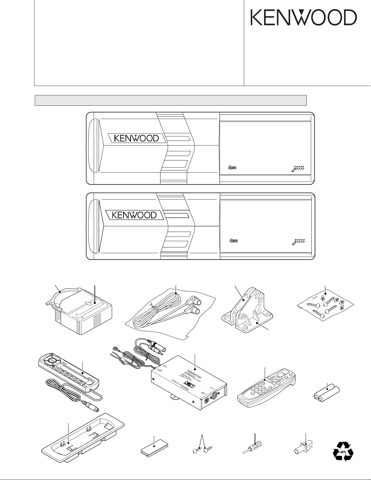
Holder assy
Tray
(J99-0614-01)
(J19-5146-02) : KDC-C521FM
(J19-5149-02) : KDC-C471FM
Cord with plug (5m)
(E30-4711-05)
COMPACT DISC AUTO CHANGER KDC-C521FM
NEW ANTI VIBRATION MECHANISM
COMPACT
CD-R/RW
DIGITAL AUDIO
COMPACT DISC AUTO CHANGER KDC-C471FM
NEW ANTI VIBRATION MECHANISM
COMPACT
CD-R/RW
DIGITAL AUDIO
Bracket
(J19-5018-03) : KDC-C521FM
(J19-5020-03) : KDC-C471FM
1BIT 4D/A CONVER
10
1BIT 4D/A CONVERTER
6
Bracket
(J19-5019-03) : KDC-C521FM
(J19-5021-03) : KDC-C471FM
DISC
DISC
Screw set
(N99-1645-15)
Control unit
(Display unit)
Unit holder
(J19-7009-08)
Velcro
(W01-1633-08)
RF Modulator
Screw
(N99-1755-08) x2
Remote controller assy
(A70-2051-05) (RC-535) : KDC-C521FM
(A70-2052-05) (RC-525) : KDC-C471FM
Size AAA battery
(Not supplied)
Except KDC-C471FM (K type)
Antenna adaptor
(T90-0512-05)
(E type only) (E type only)
Antenna adaptor
(T90-0521-05)
2
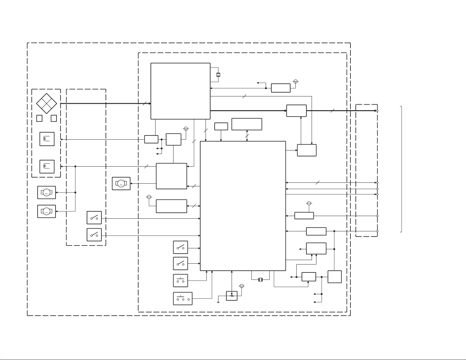
SW5V
LIM SW
L.P.S.
EJ SW
ARM SW
12.5MHz
X2
SPINDLE/LO-EJ
SLED
LOE SW
TR COIL
FO COIL
BTL
EEPROM
&TEXT DECODER
APC
SA5V
Q1
S8V
SYSTEM u-COM
IC7
IC1
RF AMP&SARVO DSP
16.93MHz
X1
P-ON
Q10
Q15,16
Q20
BU. DET
IC8
7
13
4
5
8
2
IC5
MG SW
8V AVR
S8V
S-RAM
24
C
2
BU14V
CH RST
AUDIO
OUT
5
5VREG
IC4
DA5V
S8V
3
HOT
IC9
RESET
7V/9V
5V
Q21,22
M5V1
M5V2
SW5V
S3
S2
S1
SW5V
M
M
&DC MOTOR
DRIVER
ELEVATOR
M
AVR
SA5V
Q9
&D/A CONVERTER
&SCF
MUTE
0bit
Q6,7
MUTE
Q4,5,8
SD5V
FE
A
D
B
PD
M5V2
AVR
CH-MUTE
CH-CON
5L I/F
IC11
COMM SW
S4
to
HEAD
UNIT
ASSY (X13)
(X32)
(X13)
(X92)
PICKUP
KDC-C471FM/C521FM
BLOCK DIAGRAM
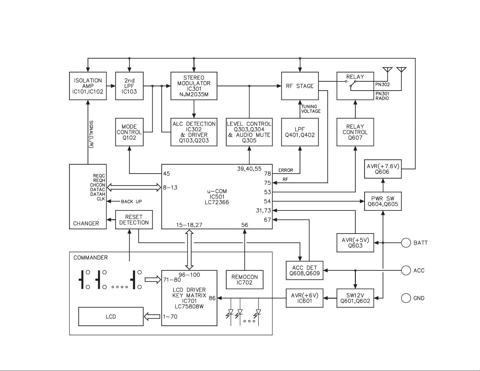
(FM MODULATOR)
BLOCK DIAGRAM
KDC-C471FM/C521FM
3
KDC-C471FM/C521FM
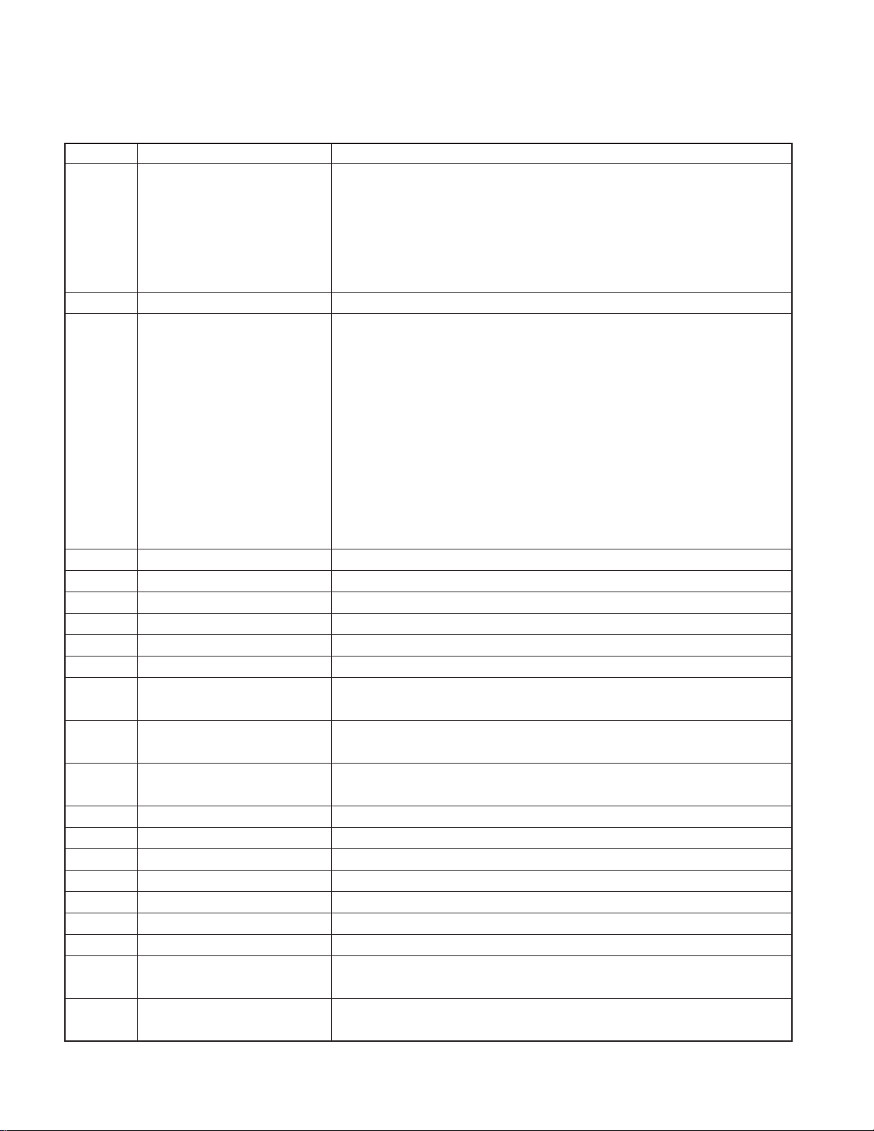
COMPONENTS DESCRIPTION
● CD PLAYER UNIT (X32-5470-01)
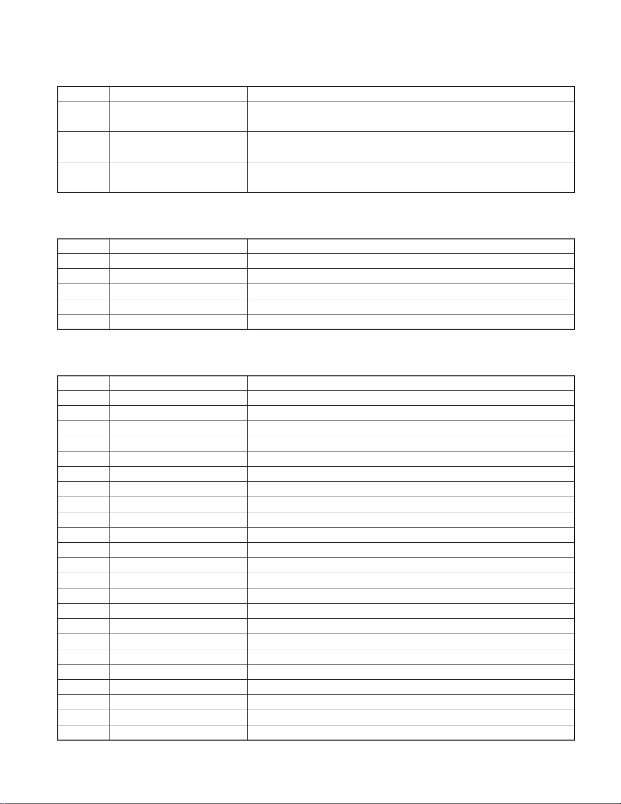
Ref. No. Application / Function Operation / Condition / Compatibility
RF amplifier built in digital servo and data processor IC. Focusing, tracking, sled and
spindle servo processing. Detection of dropout, anti-shock, track crossing and off-track
IC1 Servo IC
IC4 +5V AVR Analogue output circuit power supply for D/A converter.
IC5 Motor driver 1. Input selection.
IC7 Mechanism µ-COM Mechanism and servo control.
IC8 EEPROM LPS data back-up memory.
IC9 Reset IC When BU 5V voltage is less than 3.0V, IC outputs “Lo”.
Q1 APC Laser diode auto power control.
Q4 0 bit mute (L CH.) When 0 bit mute is activated, an emitter goes “Hi”, and Q4 outputs “Hi”.
Q5 0 bit mute (R CH.) When 0 bit mute is activated, an emitter goes “Hi”, and Q5 outputs “Hi”.
Q6 Mute SW (L CH.)
Q7 Mute SW (R CH.)
Q8 A mute drive
Q9 Servo 5V AVR Q9 is combined with IC5’s pin 26 and 27, and works as a driver of AVR.
Q10 P-ON 5V SW While base goes “Lo”, P-ON 5V is supplied to the microprocessor peripheral circuits.
Q11 Reset SW When System Reset has activated, a base goes “Hi”, and Q11 is turned on.
Q13 CH CON SW While CH CON or CH-CON2 mode is selected, a base goes “Hi”, and Q13 is turned on.
Q14 CH MUTE SW When MUTE REQUEST to H/U is outputted, a base goes “Lo”, and Q14 is turned on.
Q16 SRV 8V AVR Q16 is combined with Q15 (X92-), and works as a pre-driver of AVR.
Q17,18 SRV 8V AVR SW When Q18's base goes “Hi”, Q17 is turned on, and SVR 8V AVR is working.
Q19 7/9V SW
Q20 BU DETECTION SW
conditions.
Automatic adjustment (focusing, tracking, gain, offset and balance) operations.
Digital signal processing (DSP, PLL, sub-codes, CD-TEXT decode, CIRC error
correction, audio data interpolaration) operations.
Focusing coil, tracking coil, spindle motor and sled motor driver.
VO1~VO4 and VOL outputs ON/OFF function.
While MUTE1 goes “Hi”, VO1 outputs are turned on.
While MUTE2 goes “Hi”, VO2~VO4 and VOL outputs are turned on.
VIN1 amplifier function (input selection and VREF selection)
While VIN SW terminal goes “Lo”, IC pin 15, 16 and 17 inputs are selected.
While VIN SW terminal goes “Hi”, IC pin 15, 18 and 19 inputs are selected.
2. VREF selection.
While VIN SW terminal goes “Lo”, internal VREF (2.5V typical) is selected.
While VIN SW terminal goes “Hi”, external VREF (IC pin 30 input) is selected.
When 0 bit mute or A mute drive is activated, a base goes “Hi”, and L channel audio
signal is muted.
When 0 bit mute or A mute drive is activated, a base goes “Hi”, and R channel audio
signal is muted.
When audio mute of IC7 is activated, a base goes “Lo”, and audio mute drive signal is
outputted.
When a base goes “Hi”, Q19 is turned on, and SVR 8V AVR is outputting +7V.
When a base goes “Lo”, Q19 is turned off, and SVR 8V AVR is outputting +8.5V.
While BACKUP is applied, a base goes “Hi”, and Q20 is turned on.
When momentary power down has detected, a base goes “Lo”, and Q20 is turned off.
4
KDC-C471FM/C521FM
COMPONENTS DESCRIPTION
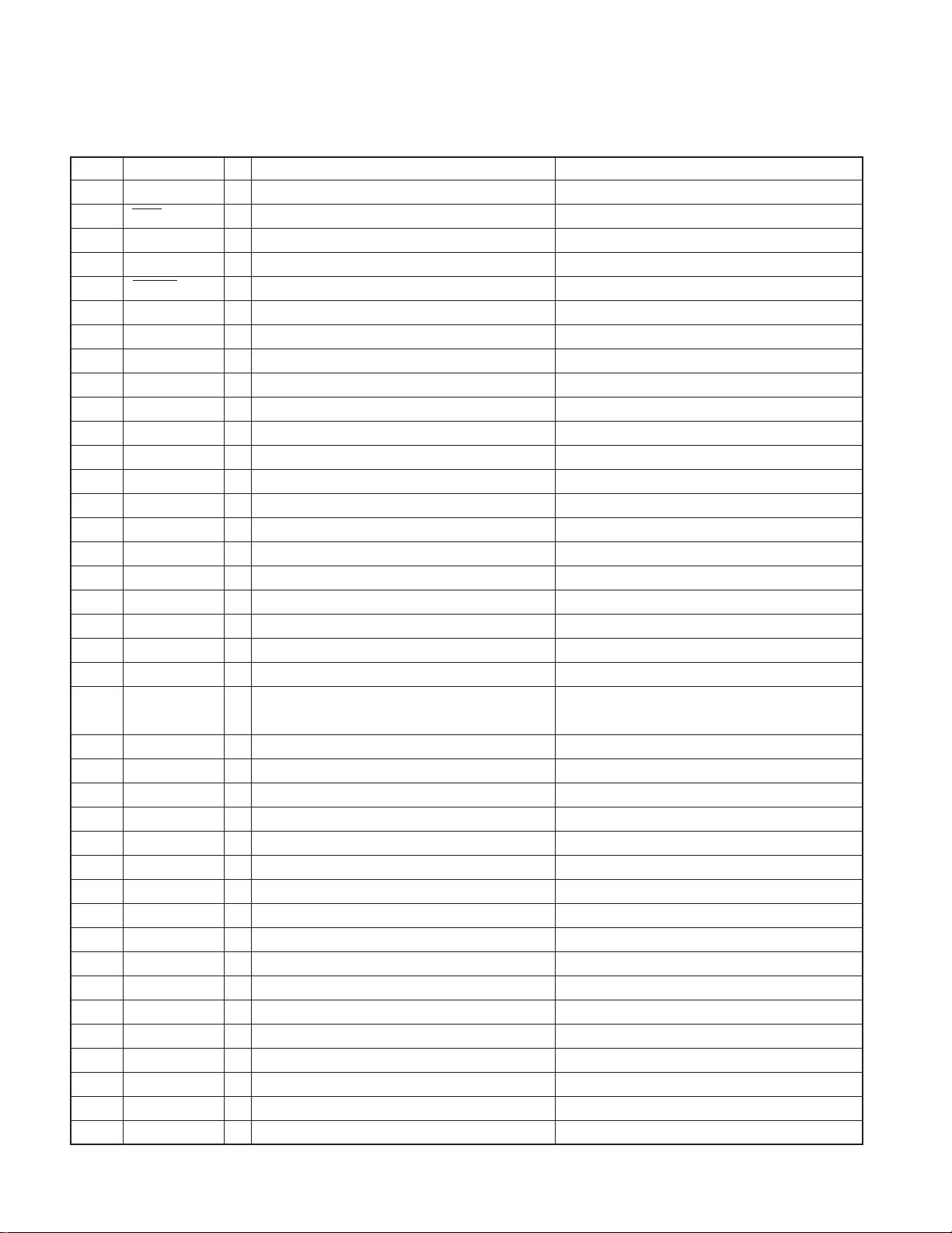
Ref. No. Application / Function Operation / Condition / Compatibility
Q21,22 BU 5V AVR
Q30 Eccentric disc SW
Q31 VIN SW
● CONTROL UNIT
Ref. No. Application / Function Operation / Condition / Compatibility
IC701 LCD Driver with Key-matrix
IC702 Remote Control Light Sensor
Q701 LED ON/OFF SW
Q702 Key-matrix Permission SW
Q703 Remote Control ON/OFF SW
While BACKUP is applied, AVR outputs +5V.
Q21 and Q22 are inverted Darlington connection.
When an eccentric disc is detected, Q30 is turned on, and a preceding beam is made to
be delayed.
While spindle servo or disc loading/eject mode is selected, a base goes “Hi”, and Q31 is
turned on.
● FM MODULATOR UNIT
Ref. No. Application / Function Operation / Condition / Compatibility
IC101,102 GND Isolation AMP
IC103 Low Pass Filter
IC301 FM Stereo Modulator
IC302 1/2 Vcc Driver, ALC Detection Amp
IC501 System µcom
IC601 6V AVR
Q102 L/R Mixer SW D.cont off : L, D.cont on : H
Q103,203 ALC Control SW
Q301 Composite Buffer
Q303,304 Level Control SW LEVEL 1/2 : L, LEVEL 3/4 : H, LEVEL 2/4 : L, LEVEL 1/3 : H
Q305 Audio Mute Power on : L, Power off : H
Q351 Temperature compensation
Q401,402 PLL Low Pass Filter
Q411 RF Amp
Q501 Changer Reset SW
Q502 Reset SW
Q601,602 Display Unit Power SW
Q603 Backup 5V AVR
Q604,605 Power SW
Q606 8V AVR
Q607 Relay Driver
Q608 ACC Detection
Q609 Hold Detection
5
KDC-C471FM/C521FM
MICROCOMPUTER’S TERMINAL DESCRIPTION
● MECHANISM MICROCOMPUTER : 784214AGC-165 (X32 : IC7)
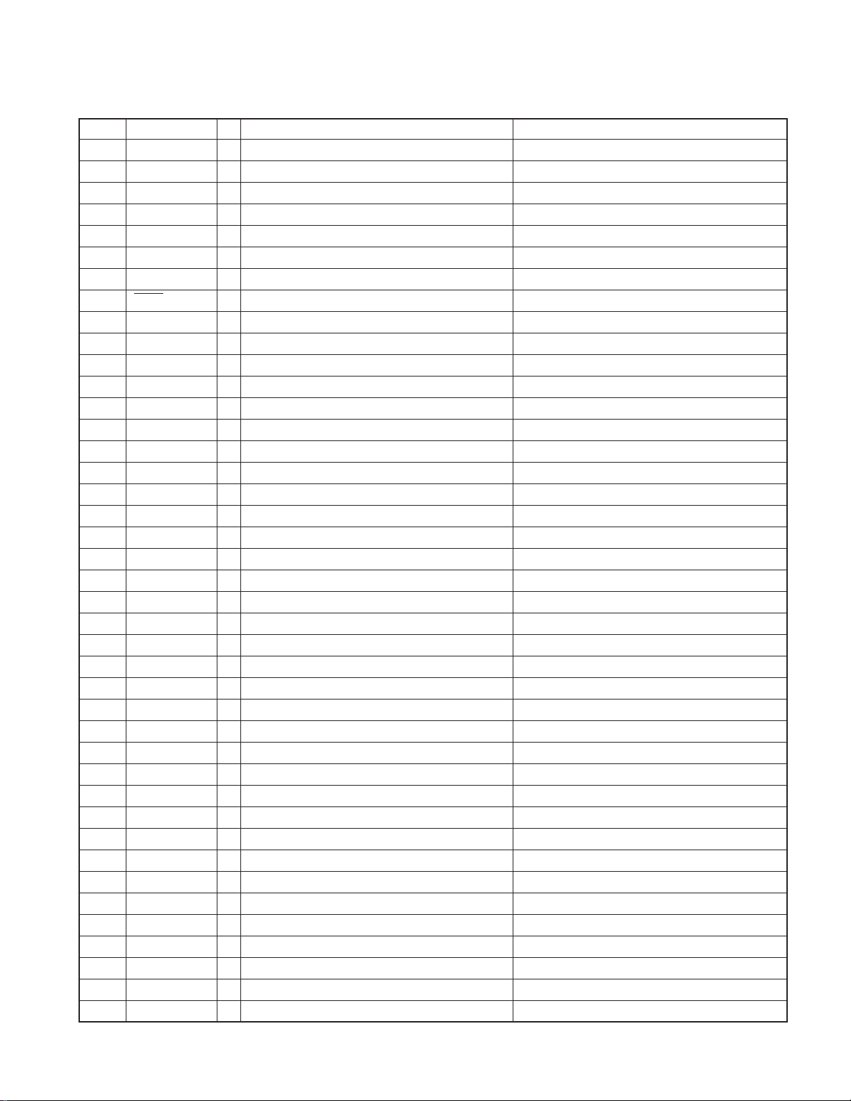
Pin No. Pin Name I/O Description Processing Operation
1 NOR/RW O CD-DA/CD-RW Switching Not used (N.C.)
2 TSTB O CD-TEXT parameter strobe
3 P-CON O P-CON output Not used (N.C.)
4 FOK I Focus OK input “Hi” : Focus OK
5XTALEN O Servo IC oscillation stop control “Hi” : Oscillation stop
6 RST O Servo IC reset terminal “Lo” : Reset
7SAO O Servo IC command/parameter setting terminal
8 SSTB O
9 VDD - Positive power supply connection terminal Connected to D 5V lines
10 X2 - Main clock resonator connection terminal 2
11 X1 I Main clock resonator connection terminal 1
12 VSS - Ground connection terminal Connected to GND lines
13 XT2 - Sub clock resonator connection terminal 2 Not used (N.C.)
14 XT1 I Sub clock resonator connection terminal 1 Not used (connected to GND lines)
15 RESET I System reset input “Lo” : System reset
16 FOGUP I Vibration detect input “Hi” : Vibration detect
17 MGSW I Magazine switch input “Hi” : Magazine in
18 EJSW I Eject switch input “Hi” : Eject switch ON
19 COMMSW I 5-line communication old/new switch input “Hi” : New communication, “Lo” : Old communication
20 PACK I Text data pack synchronous signal input “Hi”→“Lo” : The head of the pack data
21 CH-CON I Changer control input “Hi” : Standby mode, “Lo” : Operation mode
22 BUDET I Momentary power down detection input
23 AVDD 24 AVREF0 I A/D converter reference voltage input Connected to PON 5V lines
25 HOT I Rise in temperature detection input
26 LPS I LPS Mechanical deck position detection input
27 LOESW I Loading complete switch input “Lo” : Loading complete
28 LIMSW I Limit switch input “Lo” : Pickup most inner position
29 TOFF I Tracking OFF mode terminal Not used (pull down to GND lines)
30 ADJSEL I Servo automatic adjustment ON/OFF terminal Not used (pull down to GND lines)
31 TBANK I Tracking gain switching mode terminal Not used (pull down to GND lines)
32 SIM2 I Destination input 2 Not used (pull down to GND lines)
33 AVSS - A/D, D/A converter ground connection terminal Connected to GND lines
34 LPSCO O LPS A/D converter reference power control output Not used (N.C.)
35 AMUTE O Audio mute output “Lo” : Audio mute ON
36 AVREF1 I D/A converter reference voltage input Connected to D 5V lines
37 SDI I Servo IC communication serial data input
38 SDO O Servo IC communication serial data output
39 SCK O Servo IC communication serial clock output
Servo IC command/parameter setting strobe terminal
A/D converter positive power supply connection terminal
“Hi” : Parameter setting, “Lo” : Address resister setting
“Hi”→“Lo” : Serial data latch
“Hi” : When momentary power down detected or
BU OFF “Lo” : BU ON
Connected to D 5V lines
6
KDC-C471FM/C521FM
MICROCOMPUTER’S TERMINAL DESCRIPTION
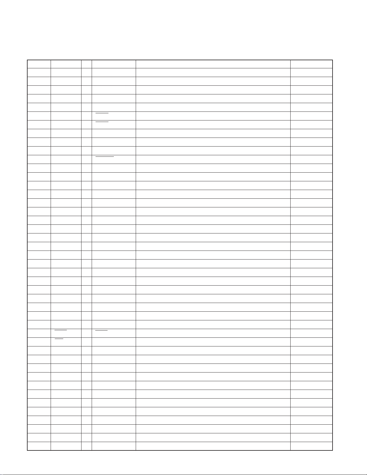
Pin No. Pin Name I/O Description Processing Operation
40 DATAH I Data input from H/U
41 DATAC O Data output from the changer
42 HCLK I/O Communication clock input/output with H/U
43 RECQC O Communication request to H/U “Lo” : Communication requested
44 CHMUTE O Audio mute request to H/U “Lo” : Audio mute requested
45 TSI I Text data input from servo IC
46 TSO O Text data output to servo IC
47 TSCK O Text data clock to servo IC
48~55 A0~A7 O Address setting terminal for S RAM
56~63 D0~D7 I/O Data input/output terminal with S RAM
64~68 A8~A12 O Address setting terminal for S RAM
69~71 A13~A15 O Chip enable setting terminal for S RAM Not used (pull down to GND lines)
72 VSS - Ground connection terminal Connected to GND lines
73 A16 O Chip enable setting terminal for S RAM Not used (pull down to GND lines)
74 A17 O Chip enable setting terminal for S RAM
75 RAMOK O Pickup check judging terminal for production Not used (N.C.)
76 ELVADJ I Mechanism deck ascent/descent position terminal Not used (pull up to D 5V lines)
77 RD O Read-out to S RAM control output
78 WR O Write to S RAM control output
79 WAIT I Waiting time insertion input when accessing S RAM Not used (pull down to GND lines)
80 ASTB O Chip selection to S RAM Not used (N.C.)
81 VDD - Positive power supply connection terminal Connected to D 5V lines
82 PUSEL I Pickup type select terminal Pull up to D 5V lines
83 REQH I Communication request from H/U “Lo” : Communication requested
84 SPLO+ O Spindle/Loading control terminal
85 SPLO- O Spindle/Loading control terminal
86 ELV+ O Mechanism deck ascent/descent terminal
87 ELV- O Mechanism deck ascent/descent terminal
88 SIM1 I Destination input 1
89 SEARCH O Search mode output Not used (N.C.)
90 TEST1 I Test mode terminal 1 for test mode Not used (pull down to GND lines)
91 TEST2 I Test mode terminal 2 for test mode Not used (pull down to GND lines)
92 8/7V O Motor driver IC power voltage control output “Hi” : 7V, “Lo” : 8.5V
93 EEPWR I EEPROM write mode terminal for production Not used (pull down to GND lines)
94 TEST/VPP I Flash ROM program mode terminal Not used (connected to GND lines)
95 SRVSEL I
96 SLNSA I Sled non-sensitive area ON/OFF terminal Not used (pull down to GND lines)
97 SDA I/O Data input/output with EEPROM
98 SCL O Clock output to EEPROM
99 PON O PON output “Lo” : AVR & LPS POWER ON
100 ARMSW I Arm switch input “Hi” : Arm switch ON
Servo active mode terminal (no mechanism movement)
“Lo” : adapted for CD-TEXT, “Hi” : not adapted for CD-TEXT
Not used (pull down to GND lines)
7
KDC-C471FM/C521FM
MICROCOMPUTER’S TERMINAL DESCRIPTION
● SYSTEM MICROCOMPUTER : LC72366-9B63 (FM MODULATOR UNIT : IC501)
Pin No. Pin Name I/O Terminal name Description
1 XIN I X IN X_tal 2 TEST2 - GND Ground connection terminal 3~5 PG3~1 O NC Not used (pull down to GND lines.) L
6 PG0 I GND Connected to GND lines. 7 PF3 O NC Not used (open) L
8 PF2 I REQC CD-Changer REQC (Active “Low”) 9 PF1 O REQH CD-Changer REQH (Active “Low”) H
10 PF0 O CHCON CD-Changer ON L
11 SI2 I CH_DATA_C CD-Changer DATA in 12 SO2 O CH_DATA_H CD-Changer DATA out L
13 SCK2 O CH_CLK CD-Changer DATA SCK (Active “Low”) H
14 PE0 O NC Not used (open) L
15 PD3 O LCD DATA out LCD Driver DATA out L
16 PD2 O LCD CLK LCD Driver CLK out L
17 PD1 O LCD RESET LCD Driver RESET out L
18 PD0 O LCD CE LCD Driver CE out L
19~26 PC3~PB0 O NC Not used (open) L
27 PA3 I LCD DATA in LCD Driver DATA in 28~30 PA2~0 I NC Not used (pull down to GND lines.) 31 VDD - Vdd 5V 32 PQ0 O NC Not used (open) L
33~44 PP3~PN0 O GAIN12~1 Modulation output switching L
45 PM3 O SEP-ATT When it has GAIN5 output, “Hi” output L
46~52 PM2~PL0 O NC Not used (open) L
53 PK3 O RELAY Antenna relay control output terminal L
54 PK2 O P-on P_ON L
55 PK1 O MUTE Mute output terminal for the Tuner frequency change L
56 INT0 I REMOCON Remote controller signal input
57~60 PJ3~0 O NC Not used (open) L
61~66 PI1~PH0 I NC Not used (pull down to GND lines.) 67 HOLD I HOLD ACC detection (Operation in HOLD “Low”) L
68 SNS I Vdd Vdd 69 LCTR I NC Not used (pull down to GND lines.) 70 HCTR I NC Not used (pull down to GND lines.) 71 EO3 O NC Not used (open) Hi-Z
72 SUBPD O NC Not used (open) Hi-Z
73 VDD - Vdd Vdd 74 AMIN I NC Not used (pull down to GND lines.) 75 FMIN I VCO in VCO input 76 VSS - Vss Vss 77 EO2 O NC Not used (open) Hi-Z
78 EO1 O Error out Phase Detector Error output Hi-Z
79 TEST1 - NC Not used (pull down to GND lines.) 80 XOUT O X-out X-tal
8
Operation in HOLD
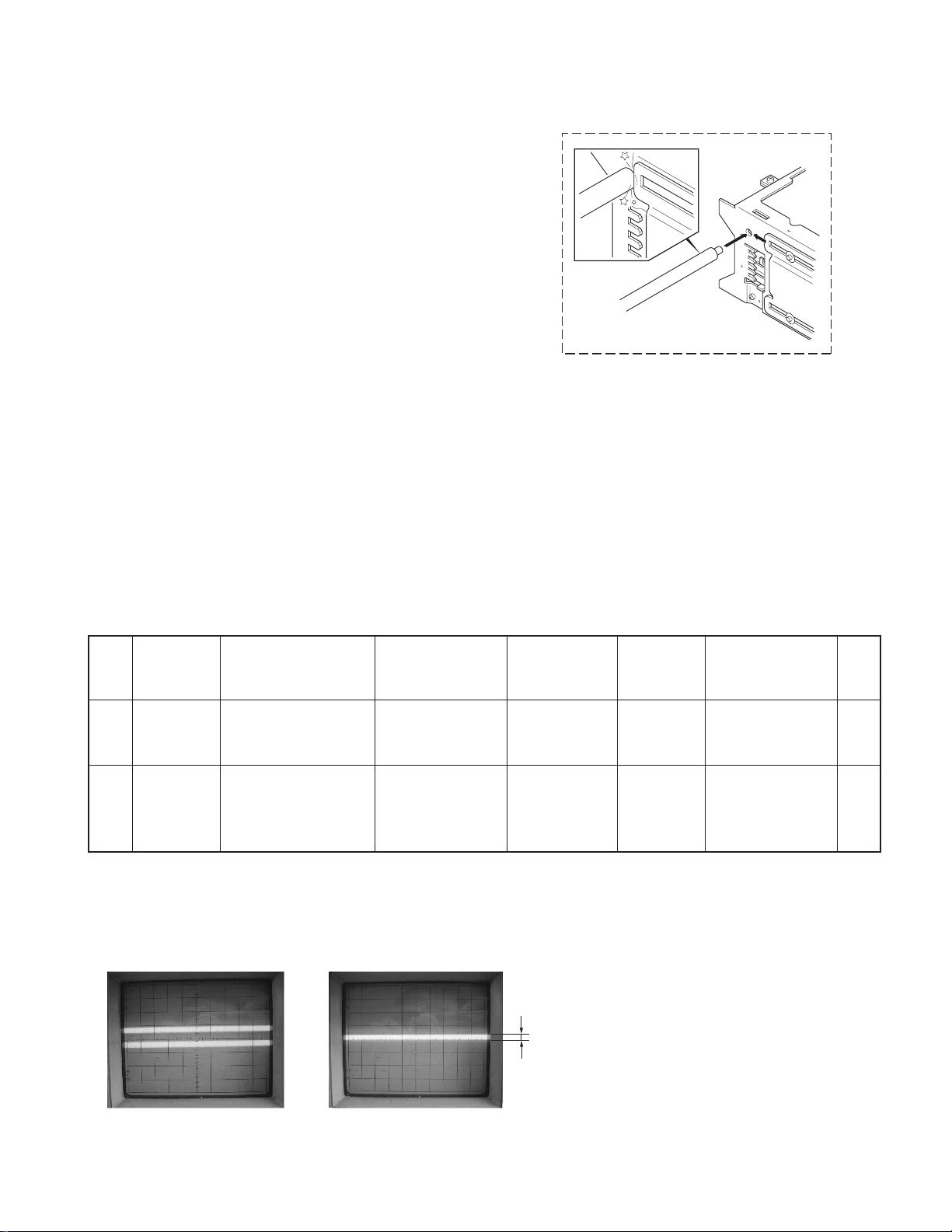
ADJUSTMENT
● L.P.S. initial position adjustment procedure
1. Connect the changer to the HEAD UNIT (H/U).
2. While holding the magazine eject button of the changer,
press the reset button of the H/U.
3. After about 3 seconds, release the magazine eject button.
4. Press the SRC button of the H/U to enter the CD-CH mode,
and the H/U's display section indicates “E-88”.
5. Move the mechanism deck to around the 1st stage by pressing the DISC- or DISC+ button.
6. Insert the adjustment tool (W05-0635-00) into the tool hole
on the changer mechanism.
7. Then press the DISC+ button to move the mechanism deck
until the mechanism's slider hits the adjustment tool.
8. When the motor locks (stops), press the REPEAT key of
the H/U.
When the REPEAT key is pressed, the mechanism moves
automatically to the 1st stage and the initial position adjustment completes. (The data is written in the EEPROM at
this time.)
KDC-C471FM/C521FM
W05-0635-00
● Caution : Note on IC8 (EEPROM)
Be sure to use the W05-0869-00 when replacing the
EEPROM. IC8 stores the digital ser vo data of the pickup
servo.
Therefore, if the EEPROM does not store servo data, ERROR76 (E-76) will indicate the H/U’ s display section at the
moment CD is played.
Instrument :
SSG, OSC (5MHz), AC VOLTMETER, PWR SUPPLY, H/UNIT, CD-CH
RECEIVER
No. ITEM INPUT SETTINGS OUTPUT SETTINGS (MODULATOR)
FREQ
L/R Balance CD-CH cignal off
1
2
(Scope Setting Condition for L/R BAL. Adj.)
1. VOLTAGE RANGE : 5mV
2. TIME/DIV : 50µs
Adj. (Tr No.29 or Pause)
Moduration
level Adj.
1. Ref.FM 1kHz 80dBµV Connect a
Stereo, CD-CH Tr No.1 AC voltmeter 88.3MHz VR302
2. D.Cont Off MOD Lv:2 to Receiver PreOut
Connect a
Oscilloscope 88.3MHz VR301 Min Level (a)
to Q301 Base.
Adjusted to be
min level point
ALIGNMENT
POINTS
* After Adj. The glue is applied to VR301, VR302.
ALIGN FOR FIG.
Difference between
FM and a CD-CH
level is adjusted to
(-0.5±1.0dB).
(Before Adj.) (After Adj.)
Fig. (a)
9
A B C D E
KDC-C471FM/C521FM
1
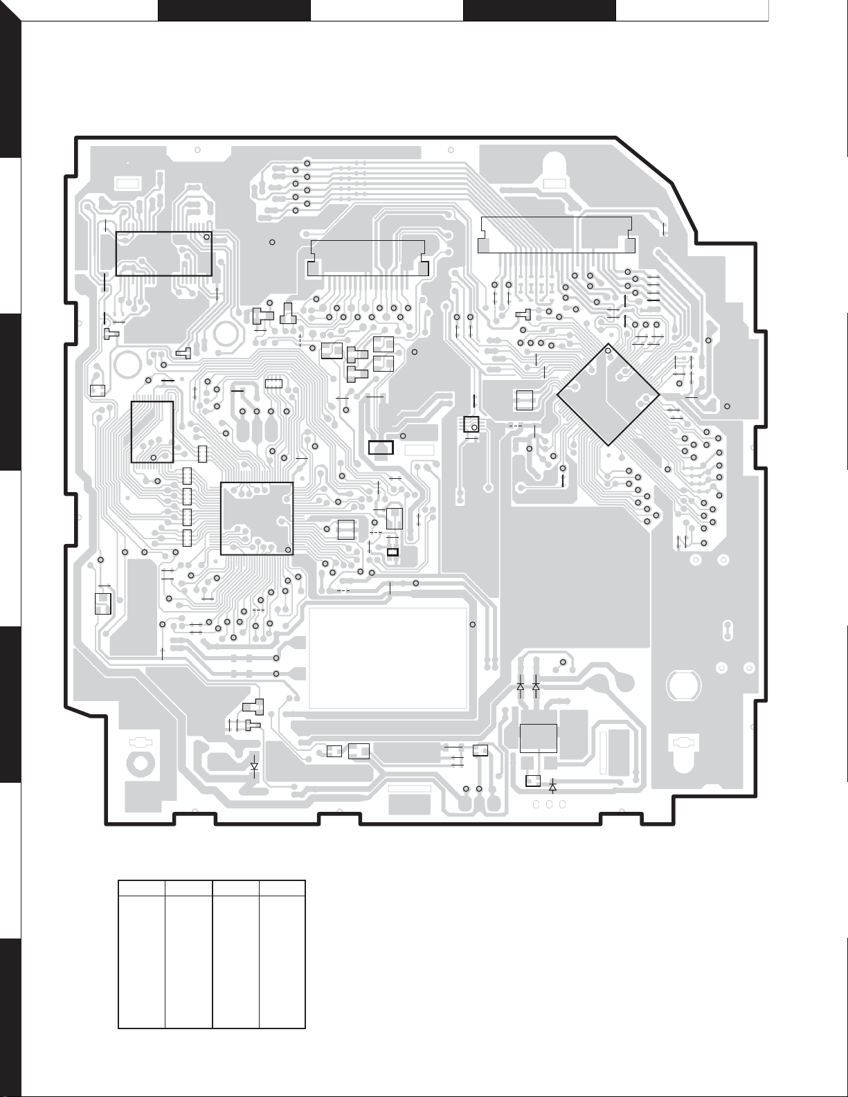
PC BOARD (COMPONENT SIDE VIEW)
CD PLAYER UNIT X32-5470-01 (J74-1527-01)
F+
T+
T-
F-
SP-
SP+
SL-
SGND
REQH
D3
R102
GND
TBANK
IC7
SRVSEL
TEST1
SEARCH
SL+
CP3
LPS
TOFF
SCL
FVPP
W5
SLNSA
ELV-
EEPRW
ELV+
D15
PCON
AMUTE
W2
FDTI
ADJSEL
C70
25
1
PON
SDA
HOT
X1
NOR/RW
/TSTB
16
FCLK
FDTO
EB
Q8
D22
R99
CHRST
PACK
D21
/CHCON
FRESET
X2
FVDD
W6
CN2
LCH
CHMUTE
CHCON
C52
C69
W7
C68
EB
EB
Q7
IC4
R97
M5V1
RCH
OGI
R106
Q11
BE
21
34
C72
Q6
1
CHRST
DA5V
R96
IC9
BU14
DAGND
R206
M5V2
Rch Lch
R54
5
IC6
8
LIMSW
R53
R145
C22
4
1
MGND
23
LOESW
R73
STB
SD5V
R72
18
2
R69
1
IC5
D24
821
R123
R105
CP6
CP12
SPLOD-
RAMOK
R122
3619
R162
TSCK
TSI
TSO
SO
CP10
50 26
CP11
51
CP5
75
76 100
WR
R134
ELV+
SIM1
ELV-
C71
AVREF
TEST2
R68
R70
R67
D23
COMMSW
R139
/CE1
3
Q31
BE
IC11
128722
/OE
SPLOD+
BE
Q20
BUDET
R76
EJSW
R126
R127
PUSEL
ELVADJ
R133
4
D7
5
C61
R77
D12
D11
Q18
EB
EB
Q17
R78
R79
C63
BU14
Q16
EB
SRV8
A0
W4
D10
Q22
D16
X1
C17
Q21
BE
CN1
VREF
RST
FOK
SCK
SO
C15
C16
25
26
ARMSW
D9
BE
F
E
SI
HOLD
R146
R4
1
A
TX
IOP-
VCC
LD
PD
IOP+
50
B
R5
R7
100
1
IC1
51
TBC
LZM
PLCK
C4
LOCK
C3
R59
C5
C
D
3TE
TE
RZM
TZC
C6
TEVCA
FZC
MIRR
R11
R12
R13
R14
FE
C9
76
75
FBAL
RFCK
R152
C7
RF
C11
DACO
A3T
R87
C10
TSTB
PACK
R16
TSI
C8
TBAL
R84
C19
SA5V
ARF
TSCK
TSO
MGSW
SAGND
ASY
EFM
MD
SD
TD
FD
D8
6
7
X32-5470-01
Ref. No. Address
IC1 3D
IC4 3C
IC5 2B
IC7 4B
IC9 4C
Q6 3C
Q7 3C
Q8 3C
Ref. No. Address
Q11 4C
Q16 5D
Q17 5C
Q18 5C
Q20 4A
Q21 5D
Q22 5D
Q31 3A
Refer to the schematic diagram for the values of resistors and capacitors.
10
JIHGF
KDC-C471FM/C521FM
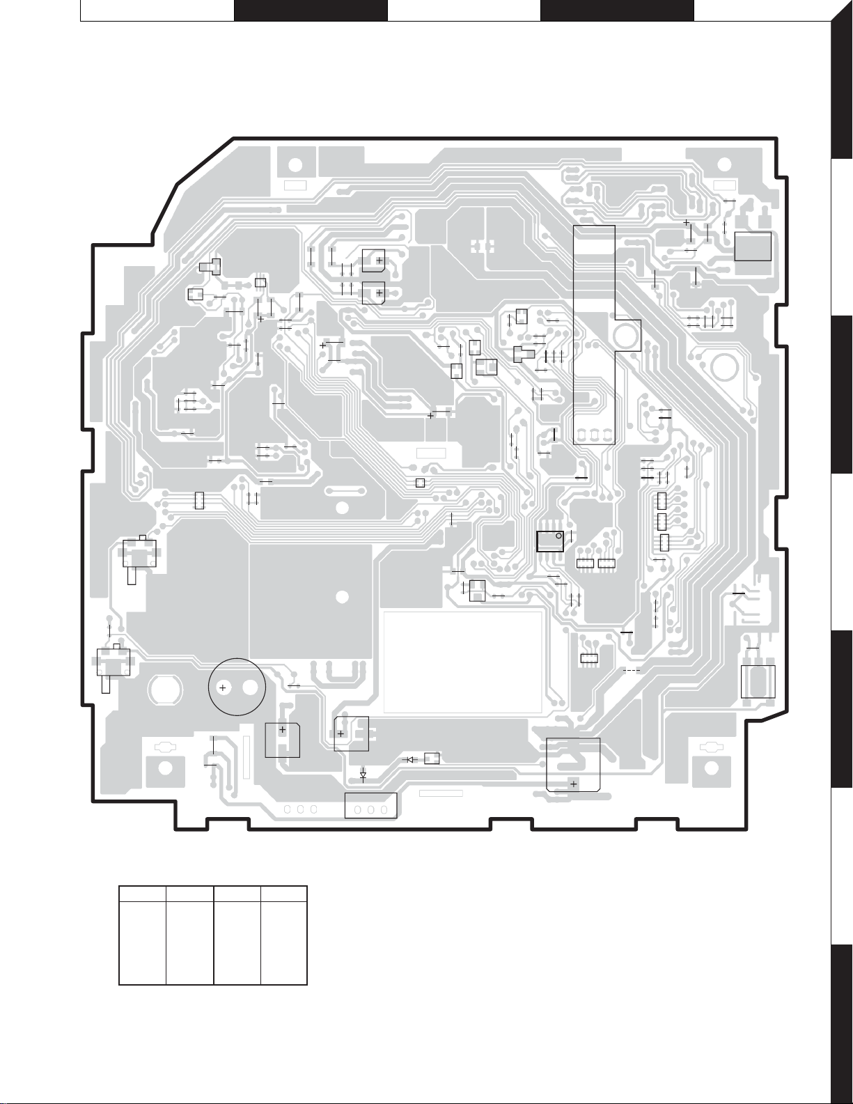
PC BOARD (FOIL SIDE VIEW)
CD PLAYER UNIT X32-5470-01 (J74-1527-01)
R60
C48
C49
R58
R57
C46
C47
R85
D1
R120
EB
C23
Q30
C205
C13
R19
R18
C12
C204
C200
CP16
S1
S3
R15
R20
C2
C206
C202
C201
L2
R9
R10
C75
Q1
R8
C14
C203
R82
R205
C24
R93
R61
C300
C301
CP9
R144
EB
Q13
C34
R95
C85
Q5
R100
BE
EB
Q4
Q10
EB
R81
R80
R121
Q14
R147
R83
EB
D4
IC8
R129
R75
R154
R98
R101
R107
R108
R148
R74
R153
TH1
R149
14
85
R150
R125
R155
C67
CP17
CP1
L.P.S
R156
CP15
C73
R143
R141
R157
W3
R17
R111
R110
CP8
R135
R142
R190
R138
R137
R136
CP7
R161
R140
CP14
C55
R22
C56
R26
R21
R25
R71
C192
C21
1
EB
2
Q9
R191
3
4
R114
R86
S2
X32-5470-01
Ref. No. Address
IC8 4H
Q1 2G
Q4 3H
Q5 3H
Q9 2J
C60
R124
Ref. No. Address
Q10 4H
Q13 3H
Q14 3H
Q19 5H
Q30 2F
C59
C62
C64
D14
BE
D5
Q15
Q19
BE
Refer to the schematic diagram for the values of resistors and capacitors.
5
6
7
11
 Loading...