Kenwood KDC-C20V Service Manual
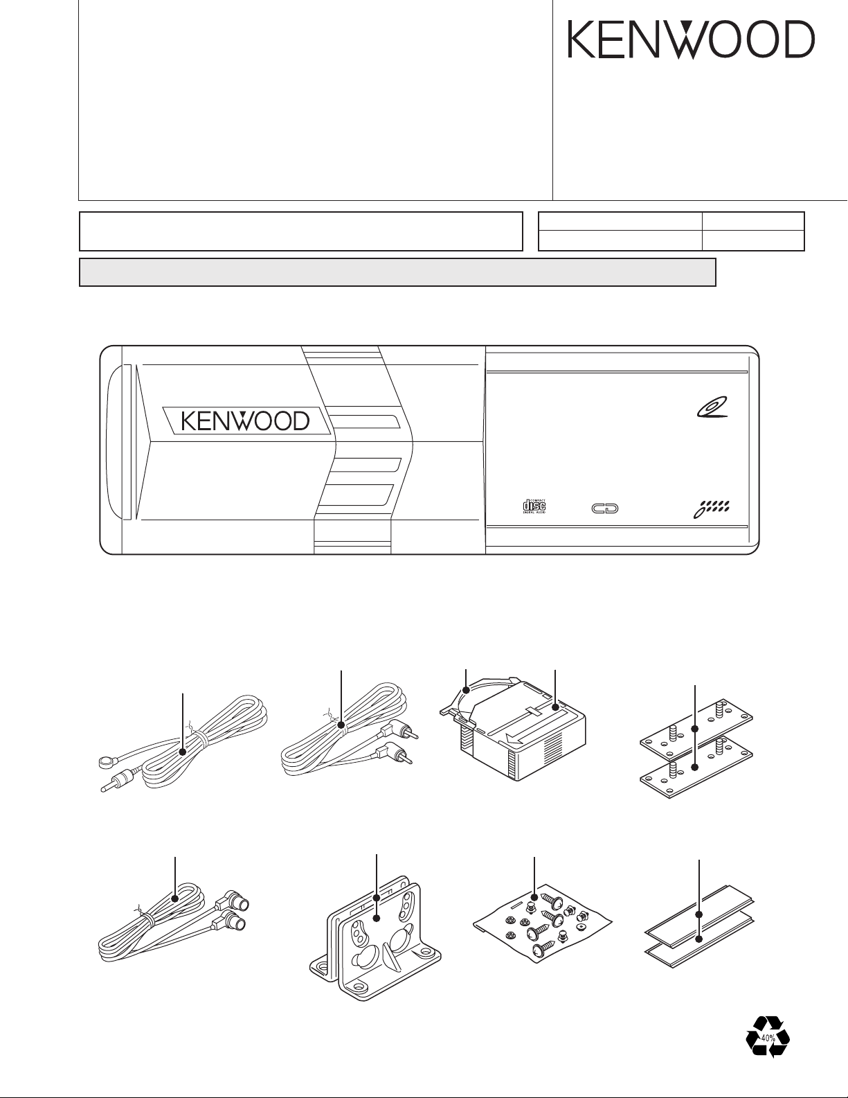
VIDEO CD/CD AUTO CHANGER
KDC-C20V
SERVICE MANUAL
© 2001-4 PRINTED IN JAPAN
B51-7786-00(S) 510
The MECHANISM OPERATION is the same as model KDC-C710.
Please refer to the service manual of model KDC-C710 (B51-7104-00).
When transporting these models, always attach CAUTION CARD and STEPPED SCREW (for transportation).
COMPACT DISC AUTO CHANGER KDC-C20V
NEW ANTI VIBRA
Service jig
For initial position setting
DISC NAME PRESET
10
CD-R/RW
TION MECHANISM
TEXT
VIDEO CD
DISC
Parts No.
W05-0635-00
REMOTE
CONTROLLER
ASSY
(A70-0876-05)
CORD WITH PLUG
(E30-4291-05)
AUDIO CORD
(E30-4586-05)
BRACKET x 2
(J19-4712-23)
TRAY
(J99-0612-01)
HOLDER ASSY
(J19-5074-02)
SCREW SET
(N99-1628-15)
MOUNTING
HARDWARE ASSY x 2
(J21-9588-04)
ADHESIVE TAPE x 2
(J69-0506-04)
KDC-C20V
SW5V
LIM SW
L.P.S
EJ SW
ARM SW
12.5MHz
X2
SPINDLE/LO-EJ
SLED
LOE SW
TR COIL
FO COIL
BTL
EEPROM
&TEXT DECODER
APC
SA5V
Q1
S8V
IC7
IC1
RF AMP&SERVO DSP
16.93MHz
X1
P-ON
Q10
Q15-19
Q20
BU. DET
IC8
7
13
4
5
8
2
IC5
MG SW
8V AVR
S8V
S-RAM
24
C
BU14V
CH RST
AUDIO
OUT
6
5V REG
IC4
DA5V
S8V
HOT
IC9,Q11
RST
7V/9V
5V
Q21,22
BU5V1
BU5V2
SW5V
S3
S2
S1
SW5V
M
M
&DC MOTOR
DRIVER
ELEVATOR
M
AVR
SA5V
Q9
&D/A CONVERTER
&SCF
BUFFER
IC6
SD5V
FE
A
D
B
PD
BU5V2
AVR
CH-MUTE
CHCON
VIDEO OUT
IC11
COMM SW
S4
SYSTEM u-COM
IC11
NTSC/PAL SW
S1
8.38MHz
X1
Q17
RST
BU5V
u-COM
DECODER
IC12
27MHz
X2
GENERETOR
IC19
CLOCK
IC13
DIR
5
IC17,18
LEVEL SHIFT
728
D-RAM
IC9
IC15
VIDEO SW
DAC
IC6
4
IC7
L.P.F. MUTE
Q15,16,18
3
A8V REG
IC1,Q1-3
BU14V
A5V REG
IC2
A5V
BU5V REG
BU14V
Q13,14
BU5V
DATAH
REQH
DATAC
CHCLK
REQC
IC5
5V SW. REG 3.3V REG
IC4
S5V
S3.3V
MONITOR
AUDIO
SW
IC10,
A8V
MPEG
ASSY (X13- )
(X32- )
(X35- )
(X92- )
PICKUP
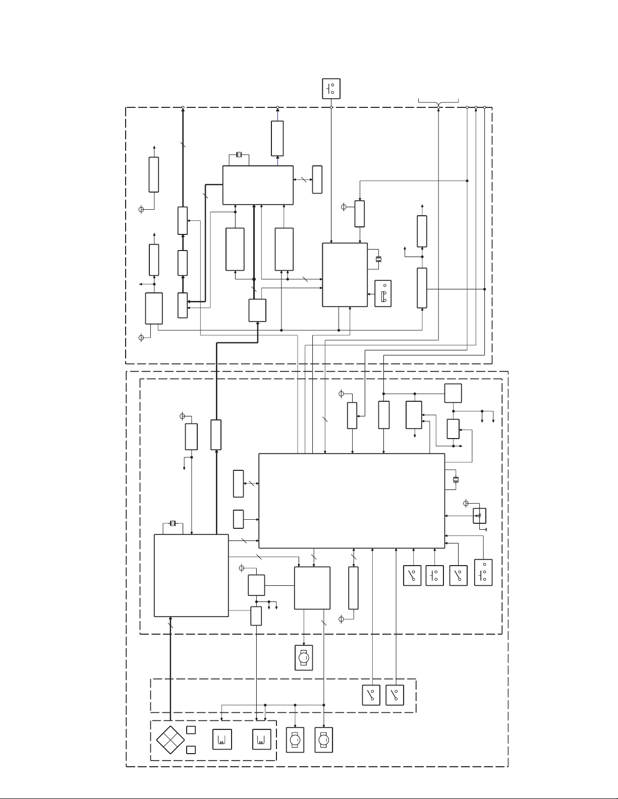
BLOCK DIAGRAM
2
KDC-C20V
COMPONENT DESCRIPTION
● CD PLAYER UNIT(X32-4960-00)
Ref.No. Component Name Application/Function Operation/Condition/Compatibility
RF amplifier built in digital servo and data processor IC. Focusing,
tracking, sled and spindle servo processing. Detection of dropout, antishock, track crossing and off-track conditions.
IC1 UPD63711AGC Servo IC Automatic adjustment(focusing, tracking, gain, offset and
balance)operations. Digital signal processing(DSP, PLL, sub-codes,
CD-TEXT decode, CIRC error correction, audio data
interpolaration)operations.
IC4 KIA78L05F +5V AVR Analogue output circuit power supply for D/A converter
Focusing coil, tracking coil, spindle motor and sled motor driver.
VO1-VO4 and VOL outputs ON/OFF function.
While MUTE1 goes "Hi", VO1 outputs are turned on.
While MUTE2 goes "Hi", VO2-VO4 and VOL outputs are turned on.
VIN1 amplifier function(input selection and VREF selection)
IC5 LA6576 4 Ch Motor driver 1. Input selection.
While VIN SW terminal goes "Lo", IC pin 15, 16 and 17 inputs are selected.
While VIN SW terminal goes "Hi", IC pin 15, 18 and 19 inputs are selected.
2. VREF selection.
While VIN SW terminal goes "Lo", internal VREF(2.5V typical) is selected.
While VIN SW terminal goes "Hi", external VREF(IC pin 30 input) is selected.
IC6 TC7WHC04FU Inverter Digital data buffer
IC7 UPD784214GC098 Mechanism MI-COM. Mechanism and servo control
IC8 W05-0870-00 EEPROM Digital servo and LPS data back-up memory
IC9 S-80830ANNP Reset IC When BU 5V voltage is less than 3.0V, IC outputs "Lo".
IC11 LC3564BT-70 S RAM CD-TEXT data memory
Q1 MCH6101 APC Laser diode auto power control
Q9 2SB1202 Servo 5V AVR
Q10 2SB1295 P-ON 5V SW
Q11 DTC124EK Reset SW
Q13 DTC124EUA CH CON SW
Q14 DTA143EUA CH MUTE SW
Q16 2SC4081 SRV 8V AVR Q16 is combined with Q15(X92-), and works as a pre-driver of AVR.
Q17 DTA143EK
Q18 DTC124EUA
Q19 DTC124EUA 7/9V SW When a base goes "Lo", Q19 is turned off, and SVR 8V AVR is
Q20 DTC124EK BU DETECTION SW When momentary power down has detected, a base goes "Lo", and
Q21 2SB1202
Q22 2SC4081 Q21 and Q22 are inverted Darlington connection.
Q30 DTC114YUA Eccentric disc SW
Q31 DTC124EUA VIN SW
SRV 8V AVR SW
BU 5V AVR
Q9 is combined with IC5's pin 26 and 27 , and works as a driver of AVR.
While base goes "Lo", P-ON 5V is supplied to the microprocessor
peripheral circuits.
When System Reset has activated, a base goes "Hi", and Q11 is turned on.
While CH CON or CH-CON2 mode is selected, a base goes "Hi", and
Q13 is turned on.
When MUTE REQUEST to H/U is outputted, a base goes "Lo", and
Q14 is turned on.
When Q18's base goes "Hi", Q17 is turned on, and SVR 8V AVR is working.
When a base goes "Hi", Q19 is turned on, and SVR 8V AVR is outputting +7V.
outputting +8.5V.
While BACKUP is applied, a base goes "Hi", and Q20 is turned on.
Q20 is turned off.
While BACKUP is applied, AVR outputs +5V.
When an eccentric disc is detected, Q30 is turned on, and a preceding
beam is made to be delayed.
While spindle servo or disc loading/eject mode is selected, a base
goes "Hi", and Q31 is turned on.
3
KDC-C20V
COMPONENT DESCRIPTION
● VIDEO UNIT(X35-4190-00)
Ref.No. Component Name Application/Function Operation/Condition/Compatibility
IC1 M5237ML AVR IC IC is combined with Q1, and it works as the error detection, the driver.
IC2 TA78L05F A. 5V AVR For D/A converter and Clock generator power supply
IC4 L88M33T D. 3.3V AVR For MPEG decoder power supply
IC5 LM2674-5.0 D. 5V AVR Output voltage 5V. A DC/DC Converter built-in the ON/OFF function.
IC6 AK4351 D/A converter
IC7 NJM4565MD OP. AMP. Low pass filter
IC9 MSM514260CP-60 D RAM 4M bit D RAM for MPEG data
IC10 PST9137NR Reset IC When BU 5V voltage is less than 3.7V, IC outputs "Lo".
IC11 UPD78011FGC573 MPEG MI-COM.
IC12 UPD61012GC-8EU MPEG decoder
IC13 CS8412-IS
IC15 MM128XFBE Video SW Video buffer buit-in 3 input select function
IC17 TC7WT126FU Buffer Signal transfer between 3.3V and 5V signals
IC18 TC7WT126FU Buffer Signal transfer between 3.3V and 5V signals
IC19 TC9246F Clock generator
Q1 2SB1184 A. 8V AVR
Q2 DTA124EUA
Q3 DTC144EUA When Q3's base goes "Hi", A.8V AVR outputs +8V.
Q4 DTA124EUA Emphasis SW Q4's base goes "Lo" during Emphasis ON.
Q5 2SA1576A
Q9 2SC4081 Video amp. 3 dB buffer
Q10 2SA1576A
Q13 2SB1184
Q14 2SC4081 Q13 and Q14 are inverted Darlington connection.
Q15 DTC343TK Audio mute SW(L Ch) When a base goes "Hi", Audio mute is activated.
Q16 DTC343TK Audio mute SW(R Ch) When a base goes "Hi", Audio mute is activated.
Q17 DTC124EUA Reset SW When Q17's base goes "Hi", MI-COM. reset is activated.
Q18 DTA144EUA Audio mute driver When Q18's base goes "Lo", Audio mute signal is outputted.
Digital Interface Receiver
A. 8V AVR SW
BU 5V AVR
Digital data decoder
A.8V AVR on/off control
While BACKUP is applied, AVR outputs +5V.
4
KDC-C20V
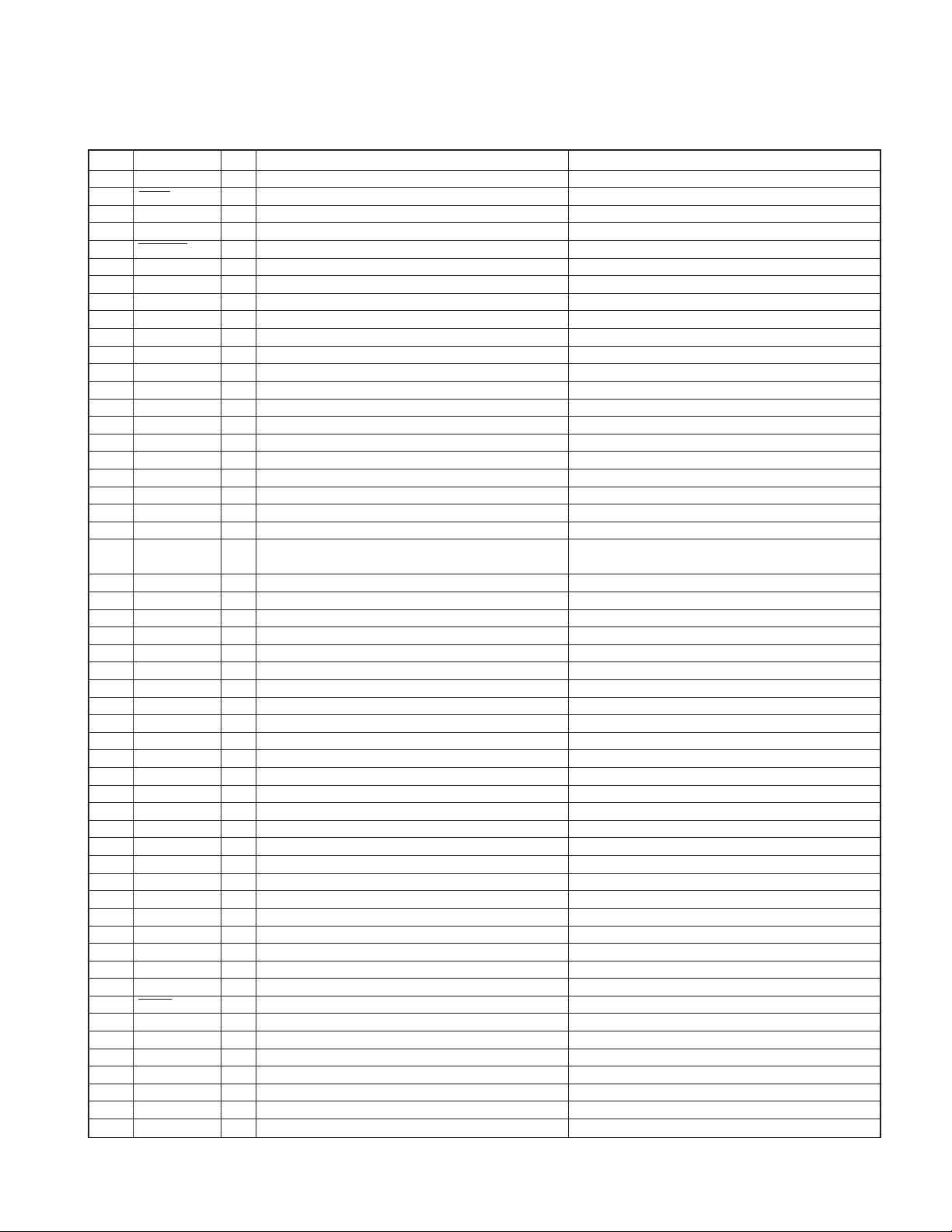
MICROCOMPUTER'S DESCRIPTION
● IC7 (CD PLAYER UNIT: X32-4960-00)
Pin No.
48-55 A0-A7 O Address setting terminal for S-RAM
56-63 D0-D7 I/O Data input/output terminal with S-RAM
64-68 A8-A12 O Address setting terminal for S-RAM
69-71 A13-A15 O Chip enable setting terminal for S-RAM Not used(pull down to GND lines)
Pin Name I/O Description Processing Operation
1 NOR/RW O CD-DA/CD-RW Switching Not used(N.C.)
2
TSTB
3 P-CON O P-CON output "Hi": POWER ON
4 FOK I Focus OK input "Hi" : Focus OK
5
XTALEN
6 RST O Servo IC & D.R.I.V.E. IC reset terminal "Lo" : Reset
7 SAO O Servo IC command/parameter setting
8 SSTB O Servo IC command/parameter setting strobe "Hi"→"Lo" : Serial data latch
9 VDD - Positive power supply connection terminal Connected to D 5V lines.
10 X2 - Main clock resonator connection terminal 2
11 X1 I Main clock resonator connection terminal 1
12 VSS - Ground connection terminal Connected to GND lines.
13 XT2 - Sub clock resonator connection terminal 2 Not used(N.C.)
14 XT1 I Sub clock resonator connection terminal 1 Not used(connected to GND lines)
15 RESET I System reset "Lo" : System reset
16 FOGUP I Vibration detect input "Hi" : Vibration detect
17 MGSW I Magazine switch "Hi" : Magazine in
18 EJSW I Eject switch "Hi" : Eject switch ON
19 COMMSW I 5-line communication old/new switch
20 PACK I Text data pack synchronous signal "Hi"→"Lo" : The head of the pack data
21 CH-CON I Changer control input "Hi" : Standby, "Lo" : Operation
22 BUDET I Momentary power down detection input
23 AVDD -
24 AVREF0 I A/D converter reference voltage input Connected to PON 5V lines.
25 HOT I Rise in temperature detection
26 LPS I LPS Mechanical deck position detection
27 LOESW I Loading completion switch input "Lo" : Loading completed
28 LIMSW I Limit switch input "Lo" : Pickup most inner position
29 TOFF I Tracking OFF mode Not used(pull down to GND lines)
30 ADJSEL I Servo automatic adjustment ON/OFF terminal Not used(pull down to GND lines)
31 TBANK I Tracking gain switching mode Not used(pull down to GND lines)
32 SIM2 I Destination input 2 "Lo": CD changer, "Hi": Video changer
33 AVSS - A/D converter ground connection terminal Connected to GND lines.
34 LPSCO O LPS A/D converter reference power control Not used(N.C.)
35 AMUTE O Audio mute "Lo" : Audio mute ON
36 AVREF1 I D/A converter reference voltage input Connected to D 5V lines.
37 SDI I Servo IC communication serial data input
38 SDO O Servo IC communication serial data output
39 SCK O Servo IC communication serial clock output
40 DATAH I Data input from H/U
41 DATAC O Data output from the changer
42 HCLK I/O Communication clock input/output with H/U
43 RECQC O Communication request to H/U "Lo" : Communication requested
44 CHMUTE O Audio mute request to H/U "Lo" : Audio mute requested
45 TSI I Text data input from servo IC
46 TSO O Text data output to servo IC
47
TSCK
72 VSS - Ground connection terminal Connected to GND lines.
73 A16 O Chip enable setting terminal for S-RAM Not used(pull down to GND lines)
74 A17 O Chip enable setting terminal for S-RAM
O CD-TEXT parameter strobe
O D.R.I.V.E. IC oscillation stop control "Hi" : Oscillation stop
"Hi" : Parameter setting, "Lo" : Address resister setting
"Hi" : New communication, "Lo" : Old communication
"Hi" : When momentary power down detected or BU OFF
"Lo" : BU ON
A/D converter positive power supply connection terminal
O Text data clock to servo IC
Connected to D 5V lines.
4V or less: Not detection, 4V or greater: Temp. detection
5
KDC-C20V
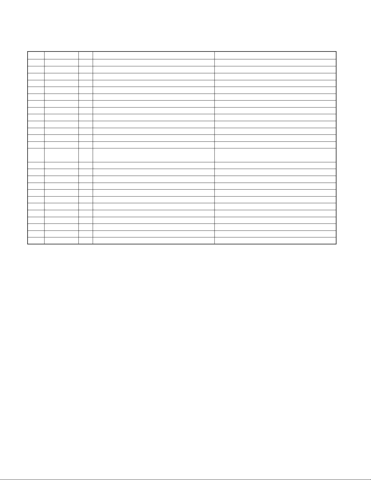
MICROCOMPUTER'S DESCRIPTION
Pin No.
Pin Name I/O Description Processing Operation
75 RAMOK O Pickup check judging terminal for production Not used(N.C.)
76 ELVADJ I Mechanism deck ascent/descent position Not used(pull up to D 5V lines)
77 RD O Read-out to S-RAM control output
78 WR O Write to S-RAM control output
79 WAIT I Wait time insertion when accessing S-RAM Not used(pull down to GND lines)
80 ASTB O Chip selection to S-RAM Not used(N.C.)
81 VDD - Positive power supply connection terminal Connected to D 5V lines.
82 PUSEL I Pickup type select Not used(pull down to GND lines)
83 REQH I Communication request from H/U "Lo" : Communication requested
84 SPLO+ O Spindle/Loading control terminal
85 SPLO- O Spindle/Loading control terminal
86 ELV+ O Mechanism deck ascent/descent terminal
87 ELV- O Mechanism deck ascent/descent terminal
88 SIM1 I Destination input 1
89 SEARCH O Search mode output Not used(N.C.)
90 TEST1 I Test mode terminal 1 Not used(pull down to GND lines)
91 TEST2 I Test mode terminal 2 Not used(pull down to GND lines)
92 8/7V O
93 EEPWR I EEPROM write mode terminal for production Not used(pull down to GND lines)
94 TEST/VPP I Flash ROM program mode Not used(connected to GND lines)
95 SRVSEL I Servo active mode (no mechanism movement) Not used(pull down to GND lines)
96 SLNSA I Sled non-sensitive area ON/OFF terminal Not used(pull down to GND lines)
97 SDA I/O Data input/output with EEPROM
98 SCL O Clock output to EEPROM
99 PON O PON output "Lo" : AVR & LPS POWER ON
100 ARMSW I Arm switch input "Hi" : Arm switch ON
Mechanism movement driver IC power voltage control
"Lo" : adapted for CD-TEXT, "Hi" : not adapted for
CD-TEXT
"Hi" : 7V, "Lo" : 8.5V
6
KDC-C20V
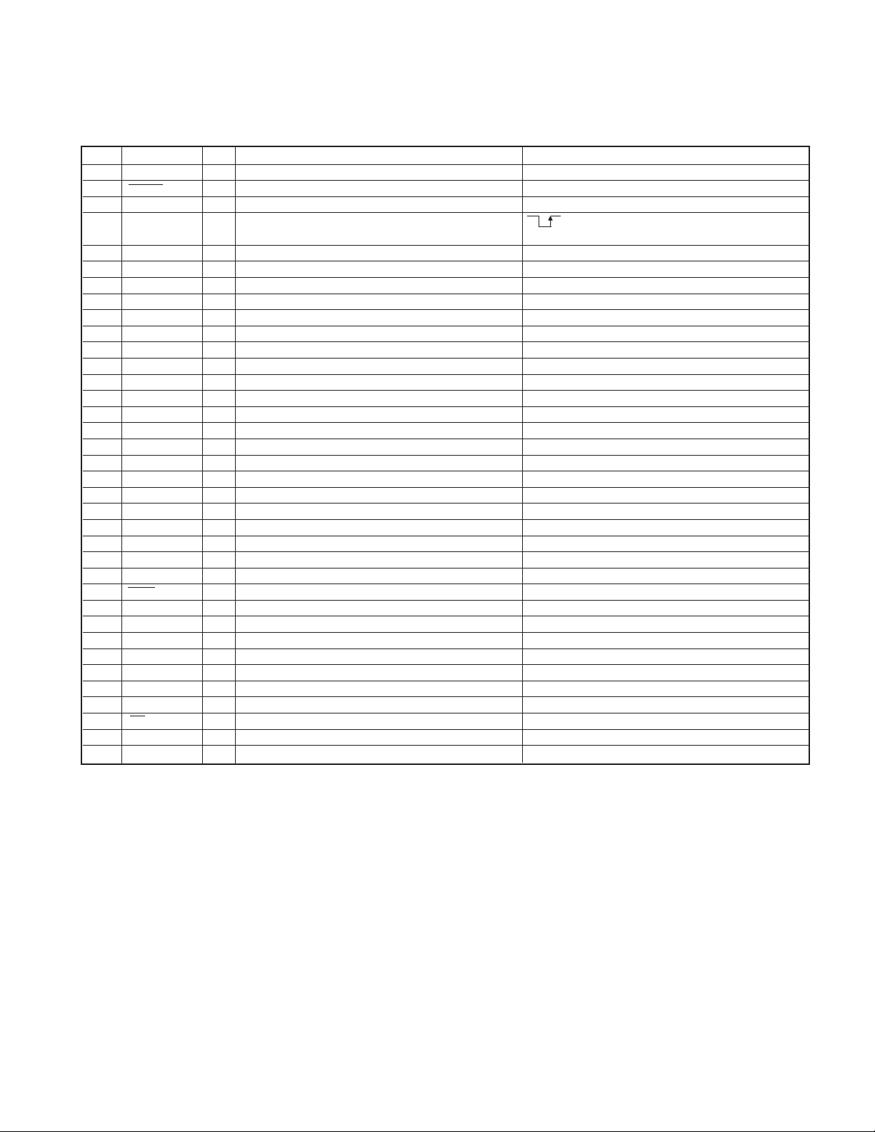
MICROCOMPUTER'S DESCRIPTION
● IC11 (VIDEO UNIT: X35-4190-00)
Pin No.
10-23 NC O Not used(N.C.)
27-34 NC O Not used(N.C.)
38,39 NC O Not used(N.C.)
47-50 NC O Not used(N.C.)
62-64 NC O Not used(N.C.)
Pin Name I/O Description Processing Operation
1 FLAG I CD error flag input "Hi": Error, "Lo": Normal
2
NTSC/PAL
3 CH/BOX I CH/BOX select terminal "Hi": CH mode, "Lo": Box mode
4 AUDIO SW I Audio monitor control input
5 P ON O P ON output "Hi" : MI-COM. peripheral circuits are activated.
6-8 NC O Not used(N.C.)
9 VSS - Ground connection terminal Connected to GND lines.
24 VSS - Ground connection terminal Connected to GND lines.
25 NC O Not used(N.C.)
26 TEST OUT O Test output Not used(N.C.)
35 RESET I System reset "Lo" : Reset
36 INT I Interrupt input from MPEG decoder
37 P CON I P CON input "Hi" : Power on mode
40 VDD - Positive power supply connection terminal Connected to BU 5V lines.
41 X2 - Main clock resonator connection terminal 2
42 X1 I Main clock resonator connection terminal 1
43 IC - Test mode terminal Not used(connected to GND lines)
44 XT2 - Sub clock resonator connection terminal 2 Not used(N.C.)
45 XT1 I Sub clock resonator connection terminal 1 Not used(connected to BU 5V lines)
46 AVSS - A/D converter ground connection terminal Connected to GND lines.
51
RESET OUT
52
VCD/CDDA
53 RSW I Audio mode setting terminal Not used(pull down to GND lines)
54 LSW I Audio mode setting terminal Not used(pull down to GND lines)
55 AVDD 56 AVREF I A/D converter reference voltage input terminal Not used(connected to GND lines)
57 SI I Serial data input from MPEG decoder
58 SO O Serial data output to MPEG decoder
59 CLK O Clock output to MPEG decoder
60
CS
61 READY I Data ready input from MPEG decoder
I Video output mode select terminal "Hi": PAL, "Lo": NTSC
: Multiple audio mode changes during VCD
playing.
O MPEG decoder reset output "Lo": Reset
I VCD/CD-DA detection input "Lo": VCD, "Hi": CD-DA
A/D converter positive power supply connection terminal
O Chip selection output to MPEG decoder
Connected to BU 5V lines.
7
 Loading...