

Kenwood KCABT-100 Service manual
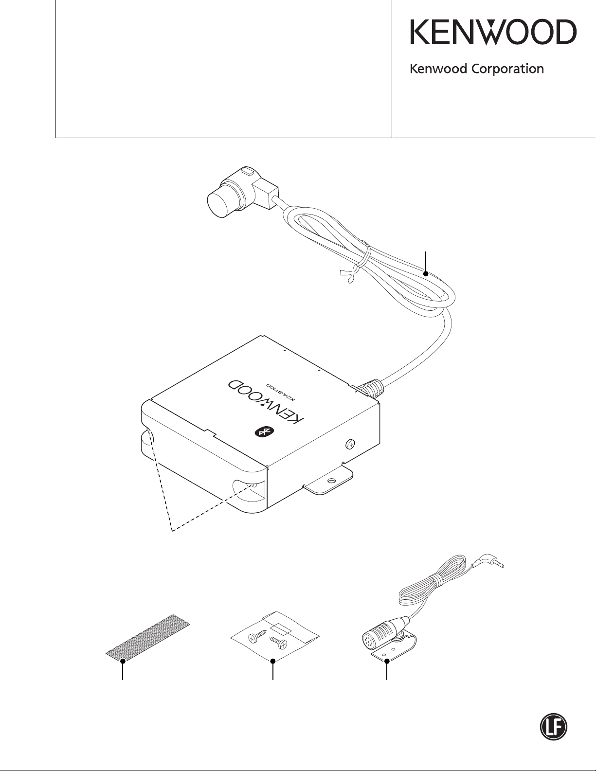
Bluetooth HANDS FREE BOX
KCA-BT100
SERVICE MANUAL
© 2006-11 PRINTED IN JAPAN
B53-0472-00 (N) 955
Cord with DIN connector
(E30-6645-05)
5L I/F
Bluetooth
About removing the 2 hexagonal head screws :
“TORX T8 Screwdriver” is necessary.
TO
IC
M
IT
UN
HEAD
TO
Bluetooth Hands Free Box
Magic tape
(H30-0600-04)
Screw set
(N99-1789-05)
Microphone (3m)
(W01-1676-05)
This product uses Lead Free solder.
KCA-BT100
BLOCK DIAGRAM
ROM CORRECTION
(NOT USED)
E2PROM
BU5V
L1
CHIP
ANTENNA
2.45GHz
2
CLK1
DATAH1
DATAC1
REQH1
REQC1
BOOT E
RESETP
RF TEST
IC6
A1 IC7
SS2
BOOT E
RESETP
SW3.3V
IC2
CLK1
DATAH1
5
DATAC1
REQH1
REQC1
MAIN
u-COM
TXD
RTS
3.3V
5V
5V
3.3V
22
TXD
RTS
BLUETOOTH
RF MODULE
SYSTEM u-COM
(LX-BUS u-COM)
BUDET
CHCON0
BU5V
RXD
RXD
22
CTS
IC5
CTS
BCLK
RELAY2
MUTE1
DX
DR
FS
CHCON2
RESET
D0
D15
A0
A18 A18
PON
PON2
CHCON1
RSTN
MUTEN
BEEP
RESET
BU5V
DX
4
DR
FS
BCLK
CODEC
SW3.3V
CLK2
DATAH2
DATAC2
CHCON1
REQH2
REQC2
CLK0
DATAH0
DATAC0
REQH0
REQC0
BU5V
16
19
PCM
5
5
MUTEN
IC8IC3
RSTN
IC4
RESET
IC
D15
J1
D0
FLASH
A0
ROM
SW5V
CONT1
CONT4
CONT2
CONT3
SELECTOR
BU5V
A8V
SW5V
SW3.3V
IC13
BPF
Q13IC11
Q3
CHCON
Q5
BU DET
Q6,16
BU5V
Q9,10
A8V
IC10
5V SW REG
IC9
3.3V REG
CH
(LX-BUS I/F)
BU
Lch2
AGND2
Rch2
MUTE2
CLK2
DATAH2
DATAC2
REQH2
REQC2
CHCON2
RESET2
J2
MIC INPUT
CN1
H/U
(LX-BUS I/F)
BU
GND
Lch0
AGND0
Rch0
MUTE0
CLK0
DATAH0
DATAC0
REQH0
REQC0
CHCON0
RESET0
COMPONENTS DESCRIPTION
● PROCESSOR UNIT (X32-5852-70)
Ref. No. Application / Function Operation / Condition / Compatibility
IC2 System µ-COM (LX-BUS µ-COM)
IC3 Main µ-COM
IC4 Reset IC Detection voltage is 3.5V
IC5 5V → 3.3V Conversion Level conversion from 5V to 3.3V
IC6 3.5V → 5V Conversion Level conversion from 3.3V to 5V
IC7 PCM Codec
IC8 Flash Memory
IC9 3.3V REG
IC10 5V REG
IC11 Analog SW Switches 5L-signal output and hands-free signal output.
IC12 MIC Input AMP Amplifies MIC input.
IC13 BPF Amplifies audio reference circuit signal and hands-free signal.
Q1 SW5V SW Vb=L: SW5V ON, Vb=H: SW5V OFF
Q2 Reset CONT Vb=H: It resets IC2 and IC3
2
KCA-BT100
COMPONENTS DESCRIPTION
Ref. No. Application / Function Operation / Condition / Compatibility
Q3 Changer CONT Vc=L: Head unit is used, Vc=H: Head unit is not used
Q5 BU DET BU ON: Vc=L, BU OFF: Vc=H
Q6 BU5V AVR Q16’s Vb=H: 5V ON
Q7,8 Analog SW CONT
Q9,10 A8V AVR Q9’s Vb=H: 8V ON
Q11 Analog SW CONT
Q12 SW14V IC3’s pin21=H: 14V ON
Q13 Audio GND SW
Q15 LX-BUS Mute Buffer IC3’s pin25=L: Vc=H, IC3’s pin25=H: Vc=L
Q16 BU5V AVR Q16’s Vb=H: 5V ON
Controls switching of IC11 and Q13
IC2’s pin22=H: Changer audio signal, IC2’s pin22=L: Hands-free audio signal
Controls switching of IC11 and Q13
IC2’s pin22=H: Changer audio signal, IC2’s pin22=L: Hands-free audio signal
Changer or Hands-free GND select SW
IC2’s pin22=H: Changer GND, IC2’s pin22=L: Hands-free GND
MICROCOMPUTER’S TERMINAL DESCRIPTION
● SYSTEM µ-COM: IC2 on X32- (PROCESSOR UNIT)
Pin No. Pin Name I/O Application Processing / Operation / Description
1~3 NC - Not used
4AVSS - A/D reference GND
5 P130 - GND
6 REQH1 O Communication request to CH1 L: Communication request is found
7AVREF1 - D/A reference voltage input
8DATAC1IData input from CH1
9DATAH1 O Data output to CH1
10 HCLK1 I/O Clock output to CH1
11 DATAH0 I Data input from head unit
12 DATAC0 O Data output to head unit
13 HCLK0 I/O Clock input from head unit
14 REQC0 O Communication request to head unit L: Communication request is found
15 REQH2 O Communication request to CH2 L: Communication request is found
16 DATAC2 I Data input from CH2
17 DATAH2 O Data output to CH2
18 HCLK2 I/O CH2 clock output
19 CHCONO1 O CH1 control output H: CH1 control request
20 CHCONO2 O CH2 control output H: CH2 control request
21 NC - Not used
22 RELA Y2 O Relay control H: CH2, L: CH1
23~32 NC - Not used
33 VSS1 - GND
34~59 NC - Not used
3
KCA-BT100
MICROCOMPUTER’S TERMINAL DESCRIPTION
Pin No. Pin Name I/O Application Processing / Operation / Description
60 RESET I Reset input L: Reset
61 REQH0 I Communication request input from head unit L: Communication request is found
62 BUDET I Detection input of momentary power down H: Detection of momentary power down
63 PO2 - GND
64 REQC2 I Communication request input from CH2 L: Communication request is found
65 REQC1 I Communication request input from CH1 L: Communication request is found
66 CHCON1 I Changer control input from head unit L: Changer control request
67 VSS0 - GND
68 VDD1 - Power supply voltage
69 X2 - Resonator connection
70 X1 I Resonator connection
71 IC - Internal connection
72 NC - Not used
73 CHCON2 I CH2 control input from head unit L: CH2 control request
74 AVDD0 - A/D anolog power supply voltage
75 AVREF0 - A/D reference voltage input
76~80 NC - Not used
● MAIN µ-COM: IC3 on X32- (PROCESSOR UNIT)
Pin No. Pin Name I/O Application Processing / Operation / Description
1,2 NC - Not used L fixed
3 LX DATA S O Data to master unit Pull-up (B.U.)
4 LX DATA M I Data from master unit
5 LX CLK I LX-BUS clock Pull-up (B.U.)
6 BYTE - External data bus switching input Connects to GND
7 CNVSS - Processor mode switching input Pull-down (GND)
8,9 NC - Not used L fixed
10 RESET I Forced reset from master unit L: Reset
11 XOUT O Main clock output
12 VSS - Power supply input Connects to GND
13 XIN I Main clock input
14 VCC1 - Power supply input Connects to B.U.5V
15 NMI I NMI interruption input Pull-up (B.U.)
16 PON2 O Circumference power supply control (5V) L: ON
17 LX CON I Start-up request from master unit H: Slave unit ON, L: Slave unit OFF
18 LX REQ M I Communication request from master unit
19 MUTEN I/O Codec mute L: Mute
20 RSTN O Codec reset L: Reset
21 PON O Circumference power supply control (A8V) H: ON
22 BEEP O Beep output 2kHz
23 BOOT E I Test mode input L: Test mode
24 RESET P I/O Module reset output L: Reset
4

KCA-BT100
MICROCOMPUTER’S TERMINAL DESCRIPTION
Pin No. Pin Name I/O Application Processing / Operation / Description
25 LX MUTE O Mute request to master unit L: Mute ON, H: Mute OFF
26 LX REQ S O Communication request to master unit Pull-down (GND)
27 ROM SCL I/O E2PROM clock for ROM correction Pull-up (B.U.)
28 ROM SDA O E2PROM data for ROM correction Pull-up (B.U.)
29 MCU RXD O Not used (Terminal for flash ROM writing) L fixed
30 MCU TXD O Not used (Terminal for flash ROM writing) L fixed
31 MCU CLK O Not used (Terminal for flash ROM writing) L fixed
32 SCIF0 RTS I Bluetooth module transmission control input
33 SCIF0 RXD O Bluetooth module data output
34 SCIF0 TXD I Bluetooth module data input
35 NC - Not used L fixed
36 SCIF0 CTS O Bluetooth module transmission control output
37 NC I Not used Pull-up (B.U.)
38 NC - Not used
39 NC I Not used Pull-up (B.U.)
40 NC - Not used
41 NC I Not used Pull-up (B.U.)
42 RD O External memory reading permission L: Reading
43 NC - Not used
44 WR O External memory writing permission L: Writing
45 NC O Not used Pull-up (B.U.)
46 DISP SEL I Switch for 2006’s models with 14-SEG display
47 A18 O External bus address Address output
48 CS O Flash ROM chip enable L: Selected
49 A17 O External bus address Address output
50 NC - Not used Open
51~59 A16~A8 O External bus address Address output
60 VCC2 - Power supply input Connects to B.U.5V
61 A7 O External bus address Address output
62 VSS - Power supply input Connects to GND
63~69 A6~A0 O External bus address Address output
70 NC - Not used Open
71~86 D15~D0 I/O External bus data Data input/output
87 FLASH RST O Flash ROM reset L: Reset
88 FLASH RY I Flash ROM ready input L: Busy (During writing)
89~93 NC - Not used L fixed
94 AVSS - Analog power supply input Connects to GND
95 NC - Not used L fixed
96 VREF - Reference voltage input Connects to GND
97 AVCC - Analog power supply input Connects to B.U.5V
98,99 NC - Not used L fixed
100 ROM WR I ROM correction writing mode input L: ROM correction writing mode
L: 2006’s models with 14-SEG display
H: Others condition (Default)
5
 Loading...