MONITOR WITH DVD RECEIVER
DDX6019/6029
/6029Y/6039
SERVICE MANUAL
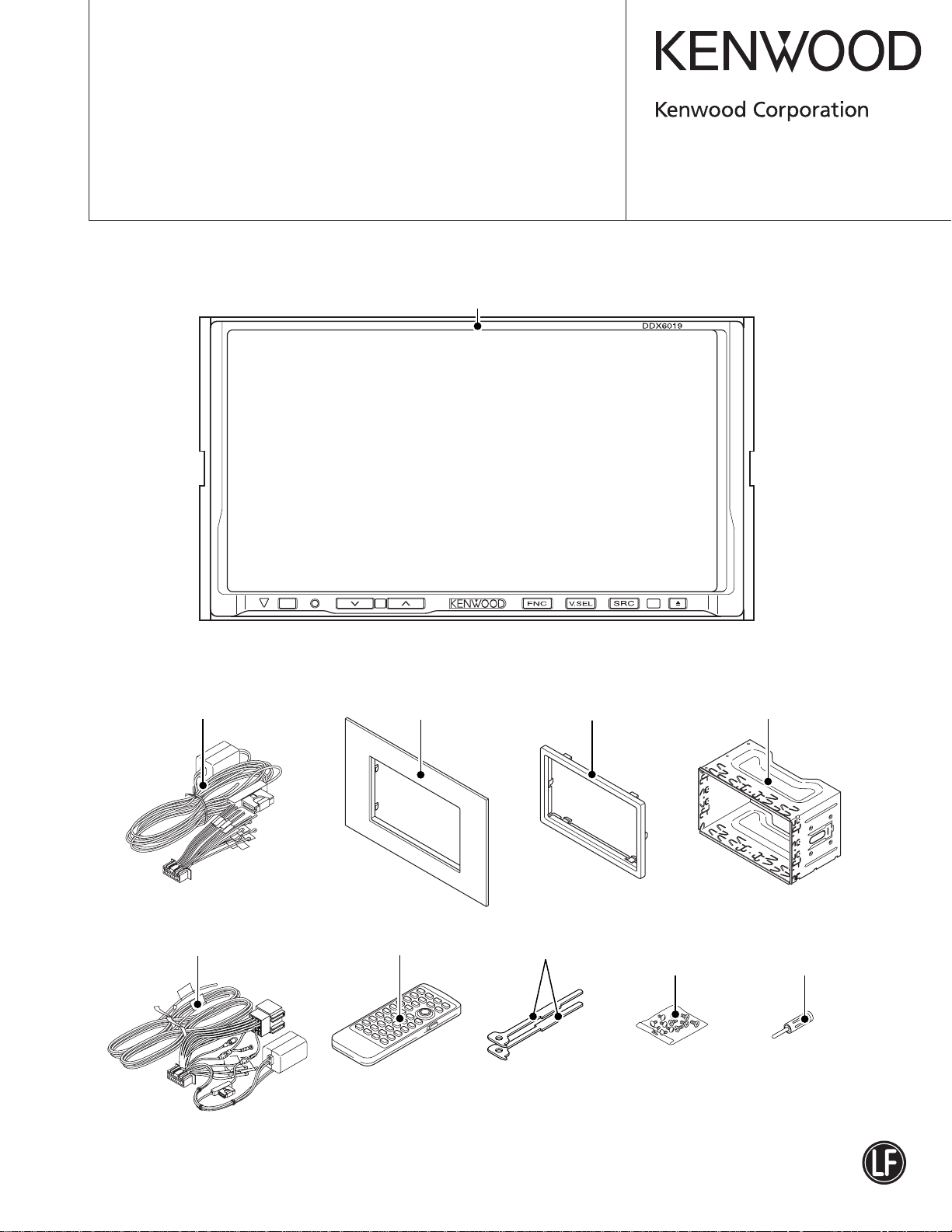
Panel assy
(A64-)*
MONITOR WITH DVD RECEIVER
© 2006-3 PRINTED IN JAPAN
B53-0390-00 (N) 960
ATT
DC cord (DDX6019/6039)
(E30-6530-05)
DC cord (DDX6029/6029Y)
(E30-6531-05)
Escutcheon
(B07-3172-12)
Remote controller assy
(A70-2077-05)
Escutcheon
(B07-3173-01)
Lever
(D10-4674-04) x 2
Screw set
(DDX6019/6039)
(N99-1776-05)
Mounting hardware
(J22-0498-03)
1
Antenna adaptor
(DDX6029/6029Y)
(T90-0552-05)
* Refer to the parts list.
RC-DV430
This product uses Lead Free solder.
2
LX-BUS
IC700
AMP
ISO
ANT.
FM/AM
FM/AM
SEL
AUDIO
IC203
SEL
IC202
AUDIO
MUTE
MUTE
MUTE
MUTE
FR
PRE
RE
PRE
PRE
SW
AUDIO
u-COM
IC101
SUPPLY
POWER
PWIC
EXTERNAL
DC CN
MUTE
AOUT
AV
E2PROM
IC301
RDS
IC251
FAN(R)
FLASH
MECHA.
DVS-7600
TV-BOX
AV IN
NAVI
ISO
AMP
IC702
SEL
IC804
V SYNC
V OUT
SEL
IC801
V IN
SEL
IC802
RGB
SEL
IC805
SYNCHRO
SEPARATOR
IC815
MOTOR
DRIVER
IC704
AV OUT
IC810
AV
VOUT
MECHA
TILT
IC201
u-COM
SYS
IC304
PDIF
S/
REMO
TOUCH PANEL & HARD KEY
E2PROM
SI
INVERTER
CHROMA
TIMING
CONTROLLER
IC3
6.95
TMD
LCD
EGA
VCOMDRIVER
IC103
IC302
IC102
OSDFROM
IC101
VMUTE 3
CAM.
BACK
MOLEX
15A
DVD
INCH
E2PROM
A
V
AUDIO (ANALOG)
CONTROL DATA
AUDIO (DIGITAL)
VISUAL (VIDEO)
VISUAL (RGB)
INPUT
SEL
AMP
ISO
AMP
ISO
&
SEL
AUX
CDCH
MD
CD
TUNER
MUXB
MUXC
AC IN 3
VOL IN
A.MUTE
E-VOL
TUNER
LX
NAVI
TV-BOX
A.SEL
RDS
AUTO SW
VIN SELECTOR/VOUT/SELECTOR/RGB SELECTOR
VSYNC DET
VOUTSEL
RGB SW
DRV
6dB AMP
MUTE
PWIC
AV IN
AV IN2
BACK CAMERA
AV IN
TV
DVD
TV-SECAM
AV IN
BACK CAMERA
NAVI SYNC
TV
DVD
VINSEL
DET
REMO
POWER
EXTERNALTILT MECHA
DVD-MECHA
COMMUNICATION
VCO
VSY
HSY
RGB OUT
V IN
OSD RGB
RGB IN
VCO
VSY
HSY
CHROMA
TIMING
TOUCH PANEL
SI
E2PROM
E2PROM
OUT
VOL
ROM CORR
VSYNC
INVERTER,
CONTROLLER
V. MUTE
ROM CORR
u-COM
75
OSD
MONITOR UNIT (X35-467)
OSD UNIT (X34-439) (A/2)
AUDIO UNIT (X14-974)
V. SELECTOR
(X34-439) (B/2)
UNIT
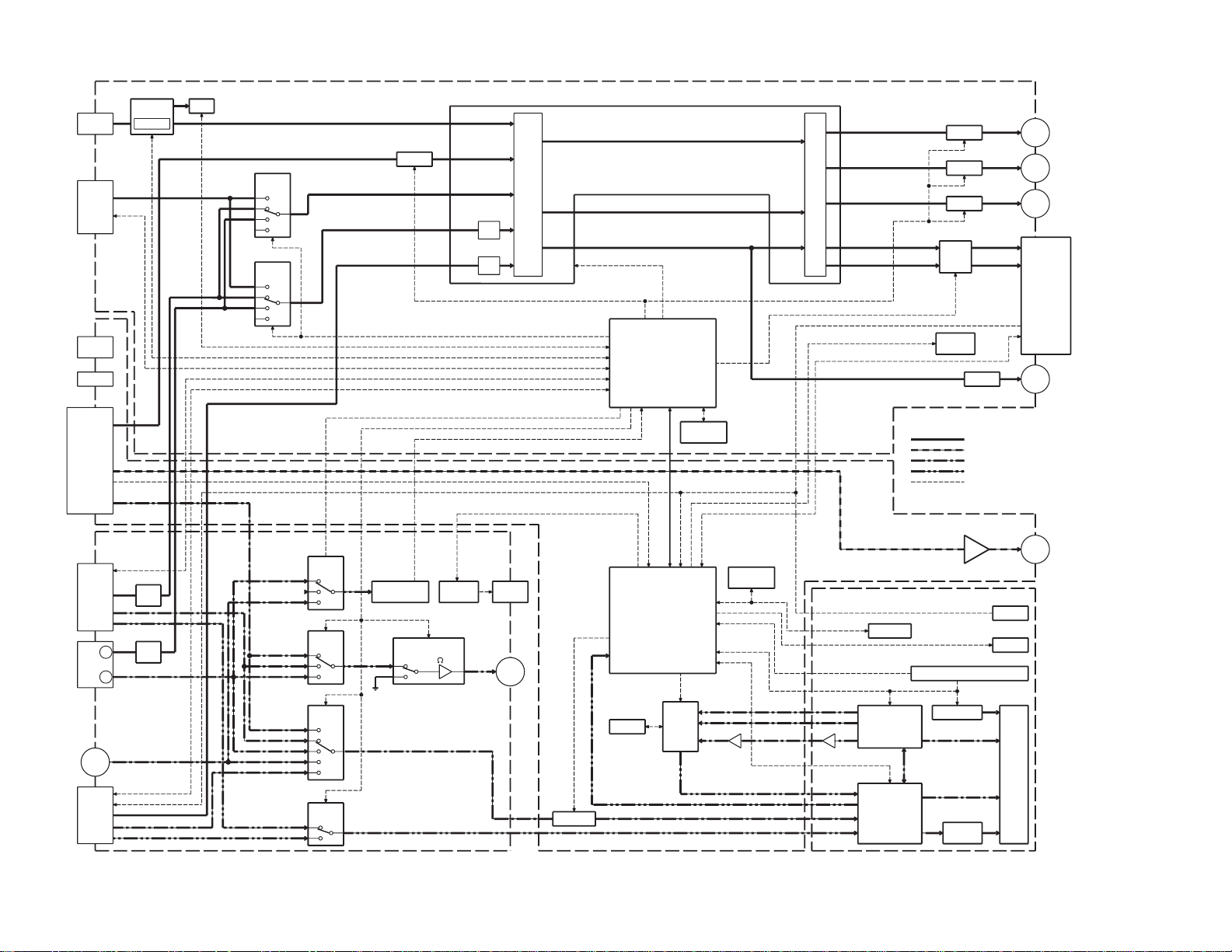
DDX6019/6029/6029Y/6039
● Complete view
BLOCK DIAGRAM
● DVD unit (X37-1150)
DISC
SPINDLE
MOTOR
HALL BIAS
U.V.W COIL
LIM-SW
P5V
LO/EJ
DC MOTOR
LOADING SW
UNIT
A
B
HALL SENSOR
CN1 :
4PIN
VPU1
A3.3V
OPTICAL PICKUP
A5V
2 PHASE
STEPPING MOTOR
3PHASE
PWM
MOTOR &
ACTUATOR
DRIVER
4
PWMx2
IC2
CN3 :
18PIN 10PIN
8
3
M
CN5 :
4PIN
PWMx2
VREF,EC
DVD LD/CD LD
VC(2.2V)
IMON/VR
I/V OUT(DVD/CD)
THERMISTER
FO+/-,TR+/-
CN2 :
P5V
VHALF
FG
C
D
E
CN11 :
30PIN
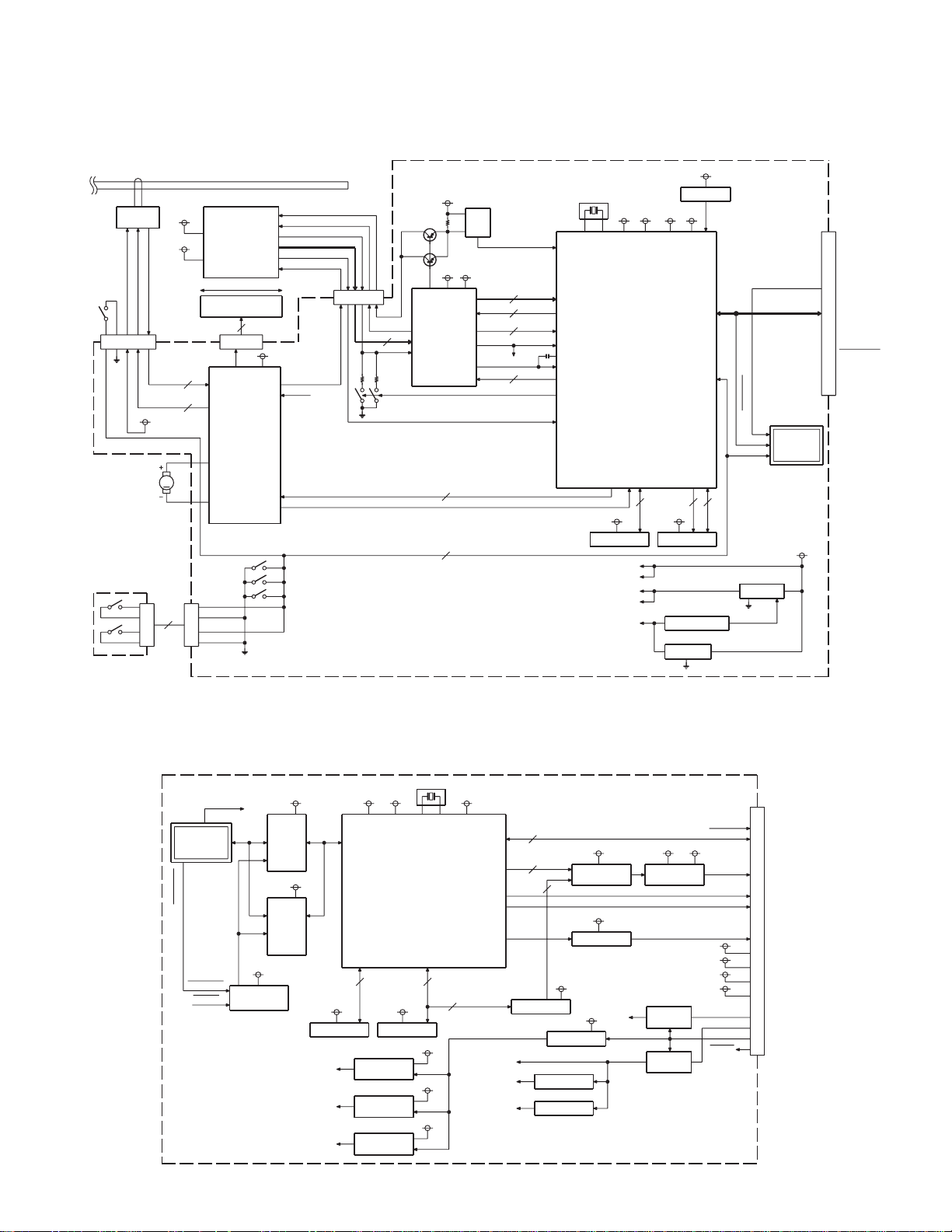
DDX6019/6029/6029Y/6039
BLOCK DIAGRAM
DVD UNIT (X37-1150-00)
Q1,2
9
Q7,8
APC
Tr
IC1
FRONT-END
PROCESSOR
A,B,C,D,E,F,
RF,FE1,FE2
SEN,SCK,STDI
A3.3V
A5V
9
6
IC65
IOP
DET
A3.3V
2
3
7
VHALF
3
16.897849MHz
IC4
LOP-(AD)
ARF,NARF
FBAL,JLINE,
TSTSG
FE,AS,RFENV,RFDIFO
OFTR,BDO,VREF2
VHALF(1.65V)
TRCRS
TE
SEN,SCK,STDI
DVDON/
CDON
TEMP
DET
S5V A3.3V 1.5VS3.3V
OPTICAL DISC
CONTROLLER
FG,EXCNT1
SDA,SCL
PWM8,DRV,MUTE,LO,MTE,
SPDRV,FODRV,TRDRV
BMS,STEP A,STEP B
28
IC11
IC3
FLASH ROMEEPROM
A5V
S5V
A3.3V
S3.3V
IC8
1.5V VOLTAGE DET
IC9
S3.3V
IC5
RESET IC
SW A,B,C,D,E
LIM-SW
FADR0-FADR17,
21
S3.3VS3.3V
1.5V REG
NRST
ATAPI IF
DISC DET
NCE,NWE,NOE
FDT0-FDT7
BUS OPEN
ATAPI IF
IC10
3.3V REG
ON/OFF
to
2/2 SHEET
S5V
CN10 :
40PIN
BUS OPEN
DISC DET
from
2/2 SHEET
BUS OPEN
BUS OPEN
BE RST
BUS SW CONTROL
D5V
LOGIC
IC48
BUS-SW
IC42
BUS-SW
IC56
D5V
D5V
ATAPI IFATAPI IF
IC51
BE3.3V
BE2V
IC30
D3.3V
SDRAM
4V
BE3.3V
BE2V BE3.3V
AV DECODER
38
IC50
FLASH ROM
IC54
3.3V REG
IC52
2.0V REG
IC46
4.0V REG
D3.3V
27.00MHz
(MPEG)
33
D5V
M3.3V
D5V
BE CLK
BE REQ
A VEE
BE DAT
SYS REQ
SYS DAT
MCLK
BCLK
LRCK
SDT
5
POWER ON/OFF CONTROL
IC57-60
LOGIC
AD8V
AD5V
AD4V
5
4
DAC
IC40
IC53
AD5V
IC12
2ch DAC ACTIVE-LPF
4
4V
IC47
VIDEO-AMP
CONTROL
BE3.3V
M3.3V
IC56
LOGIC
5.0V REG
OP-AMP
5LINE-BUS (KW PROTOCOL)
IC41
Q17
D3.3V
Q18
AD8V AD4V
AUDIO OUT
S/P DIF
VIDEO OUT (COMPOSIT)
P5V
S5V
D5V
M3.3V
SW
BE RST
SW
CN9 :
50PIN
DISC DET
Lch/Rch
A MUTE
VOUT
D3.3V
A8V
BE PON
3

DDX6019/6029/6029Y/6039
COMPONENTS DESCRIPTION
● RECEIVER UNIT (X14-974x-xx)
Ref. No Application / Function Operation / Condition / Compatibility
IC1 Logic IC (NOR x 4) Hard MUTE DRIVER
IC5 3 terminal regulator Audio8V, Tuner8V generating
IC101 100 pin µ-com Primarily, audio board control
IC104 Voltage detector µ-com reset voltage (4.2V) monitoring
IC105 Logic IC (inverter) Reverse reset from X34
IC201 Electronic volume IC Audio volume control and audio signal selection
IC202 Logic IC (multi plexer) Audio signal selection (Sub)
IC203 Logic IC (multi plexer) Audio signal selection (Main)
IC204 Logic IC (AND) DVD_MUTE 3.3V→5V conversion
IC251 RDS decoder IC For RDS signal processing and demodulating
IC301 Power IC Power amplifier for speaker output
IC401 Isolation amplifier IC For audio signal GND isolation (LX-CH)
Q1 Transistor Parking detection circuit
Q2 Transistor Reverse detection circuit
Q3 Transistor ILLMI detection circuit
Q4 Transistor ACC detection circuit
Q14,16 Transistor Bu detection circuit
Q18~21 Transistor P_CON output circuit
Q22,23 Transistor ANT_CON output circuit
Q24 Transistor EXT_CONT output circuit
Q25 Transistor Generating Bu5V
Q26 Transistor Bu5V circuit
Q27,28 Transistor SW5V circuit
Q29 Transistor SW14V circuit
Q30 FET SW14V circuit
Q31,32,34 Transistor Hard MUTE circuit
Q42~44 Transistor
Q45 T r ansistor Audio8V, Tuner8V generating
Q101~103 Transistor µ-com reset circuit
Q201 Transistor Audio SEL circuit (ASEL4)
Q202 Transistor Audio SEL circuit (ASEL3)
Q203 Transistor Audio SEL circuit (ASEL2)
Q204 Transistor Audio SEL circuit (ASEL1)
Q205,206 Transistor DVD_MUTE
Q207 Transistor DVD_MUTE circuit
Q253,255 Transistor On when AM (Tuner8V)
Q301 Transistor Pre-Out Mute (FL)
Q302 Transistor Pre-Out Mute circuit (Front, Rear)
Q303 Transistor Pre-Out Mute (FR)
4

DDX6019/6029/6029Y/6039
COMPONENTS DESCRIPTION
Ref. No Application / Function Operation / Condition / Compatibility
Q304 Transistor Pre-Out Mute (RL)
Q305 Transistor Pre-Out Mute (RR)
Q306 Transistor Pre-Out Mute (SUB L)
Q307 Transistor Pre-Out Mute circuit (SUB)
Q308 Transistor Pre-Out Mute (SUB R)
Q309 Transistor Pre-Out Mute (AV-OUT L)
Q310 Transistor Pre-Out Mute circuit (AV-OUT)
Q311 Transistor Pre-Out Mute (AV-OUT R)
● ELECTRIC UNIT (X34-439x-xx)
Ref. No Application / Function Operation / Condition / Compatibility
IC1,2 DC-DC control IC DC-DC circuit control/drive
IC3 5.0V 3 terminal regulator Power supply for S5.0V
IC4 5.0V 5 terminal regulator Power supply for D5.0V
IC5 3.3V 5 terminal regulator Power supply for D3.3V
IC60 3.3V 3 terminal regulator Power supply for BU3.3V
IC101 OSD ROM ROM for OSD display
IC102 OSD IC IC for OSD display
IC210 Inverter For amplifying clock for OSD
IC211 AND HSYNC delay
IC301 AND 3.3V→5.0V conversion
IC302 E2PROM Nonvolatile memory
IC303 RESET IC For SYSCOM reset
IC304 SYS µCOM System control
IC305 AND Remote control and wired remote control
IC401 OR Buffer for SPDIF
IC600 DC-DC control IC DC-DC circuit control/drive
IC601 Schmitt trigger inverter Remote control waveform shaping
IC603 AND VSYNC delay
IC700 ISO AMP For TV_R, TV_L
IC702 ISO AMP For AVIN1_R, AVIN1_L
IC703 AND Buffer for NAVI_REMO
IC704 Motor driver For tilt mechanism
IC801 SW for AVOUT Selection of TV, AVIN1, DVDIN
IC802 SW for VIN Selection of TV, AVIN1, DVDIN, BCAME, NAVISYNC
IC804 SW for sync separation Selection of BCAME, AVIN1/AVIN2
IC805 Video SW Selection of TV R/G/B, NAVI R/G/B
IC810 Driver 75Ω driver and 6dB amplifier
IC812 5.0V 3 terminal regulator Power supply for SW5.0V
5

DDX6019/6029/6029Y/6039
COMPONENTS DESCRIPTION
Ref. No Application / Function Operation / Condition / Compatibility
IC815 Sync separation IC Sync separation
Q3,5 Short detection circuit For SW5.0V
Q7,8 Short detection circuit For SW8.5V
Q60,61 SW For SW3.3V
Q101 Emitter follower Current amplification and buffer for OSD_R signal
Q102 Emitter follower Current amplification and buffer for OSD_G signal
Q103 Emitter follower Current amplification and buffer for OSD_B signal
Q105,106 Emitter follower Current amplification and buffer for X35_VIN
Q301 SW For X34_RST
Q302 SW For KEY_RESET
Q307,308 SW For SI
Q404 Emitter follower Current amplification and buffer for DVS_DVDIN
Q600,601 Short detection circuit For BL9.0V
Q602,603 SW For KEY_ILL
Q800 Emitter follower Current amplification and buffer for ROUT
Q801 Emitter follower Current amplification and buffer for GOUT
Q802 Emitter follower Current amplification and buffer for BOUT
Q803 Emitter follower Current amplification and buffer for VIN
Q804 MUTE circuit For ROUT
Q805 MUTE circuit For GOUT
Q806 MUTE circuit For BOUT
Q807 MUTE circuit Reverse
● VIDEO UNIT (X35-467x-xx)
Ref. No Application / Function Operation / Condition / Compatibility
IC1 AND IC3 VSYNC input signal buffer
IC2 NOT HSY signal reverse
IC3 Timing controller LCD drive timing control IC
IC4 LPF PLL circuit
IC5 Flip-flop HSY, VSY phase matching circuit
IC6 3 state buffer HSY, VSY phase matching circuit
IC7 NAND 2/3 divided circuit
IC8 NOR 2/3 divided circuit
IC9 2-in-1 flip-flop 2/3 divided circuit
IC11 NOT 2/3 divided circuit
IC12 AND 2/3 divided circuit
IC13 OR 2/3 divided circuit
IC14 NOT 2/3 divided circuit
IC100 One shot Timing matching
6

DDX6019/6029/6029Y/6039
COMPONENTS DESCRIPTION
Ref. No Application / Function Operation / Condition / Compatibility
IC101 OR IC103 video switching signal line
IC102 NOT Makes the signal negative
IC103 Chroma γ IC Chroma decoder, γ correction video signal processing IC
IC104 AND IC103 VMUTE signal line
IC106 NOT Reversing video mask signal from IC3
IC200 5V regulator Video system 5V generation
IC201 3.3V regulator Video system 3.3V generation
IC202 DC/DC, Charge pump Power supply generation for LCD
IC204 Inverter IC For inverter transformer drive
IC205 E2PROM Saving γ adjustment value, etc.
IC207 5V regulator IC202 power supply
Q1 Oscillating circuit PLL circuit
Q2 For Reversing HSY, VSY phase matching circuit
Q3~6 Buffer 2/3 divided circuit
Q100 Buffer Composite signal line
Q102 Mute C. SYNC line
Q103 Buffer B signal line
Q104 Buffer G signal line
Q105 Buffer R signal line
Q106 Buffer VCOM signal line
Q107 For reversing Switching NTSC/PAL *For 2-71 destination only
Q208 5V AVR IC204 5V power supply generation
Q210 For reversing IC204 PWM signal line
Q215 Switching FET Full bridge construction with Q216
Q216 Switching FET Full bridge construction with Q215
Q217~220 Switching Touch panel I/F
Q221 For reversing Touch panel I/F
● DVD UNIT (X37-1150-00)
Ref. No Application / Function Operation / Condition / Compatibility
IC1 RF signal processing IC RF signal processing
IC2 Driver Driver for each motor / pick-up actuator
IC3 FLASH ROM Maintaining FW for optical disc control IC
IC4 Optical disc control IC in µ-com Optical disc general control / ATAPI interface
IC5 Voltage detection IC For resetting optical disc control IC
IC8 Voltage detection IC For power supply voltage monitoring
IC9 Power supply IC for S1.5V S5V→S1.5V
IC10 Power supply IC for S3.3V S5V→S3.3V
IC11 EEPROM Maintaining data for optical disc control IC
7

DDX6019/6029/6029Y/6039
COMPONENTS DESCRIPTION
Ref. No Application / Function Operation / Condition / Compatibility
IC12 2ch D/A converter Convert audio digital signal to analog signal
IC30 DVD processor MPEG decoder function processor (AV decoder)
IC40 Power supply IC for A5V A8V→ A5V
IC41 OP-AMP (with 2 circuits) For analog audio signal active LPF
IC42 20bit BUS-SW FE portion's ATAPI connection destination switching
IC46 Power supply IC for video AMP D5V→4V
IC47 Video AMP 6dB amplifier with LPF
IC48 8bit BUS-SW FE portion’s ATAPI connection destination switching
IC50 FLASH ROM FW maintaining for DVD processor
IC51 SDRAM IC SDRAM for DVD processor
IC52 Power supply IC for BE2V M3.3V→BE2V
IC53 OP-AMP (with 1 circuit) Buffer for analog audio reference potential
IC54 Power supply IC for BE3.3V D5V→BE3.3V
IC56 CMOS logic IC FE portion's ATAPI connection destination switching control
IC57~61 CMOS logic IC D/A converter control
IC62 CMOS logic IC BE-PON signal output level assurance
IC65 Rail-to-rail OP-AMP Buffer for IOP value detection
Q1 MOS-FET Laser diode for DVD ON/OFF control
Q2 MOS-FET Laser diode for CD ON/OFF control
Q7 Transistor for APC Laser diode for CD brightness volume control
Q8 Transistor for APC Laser diode for DVD brightness volume control
Q9 MOS-FET For protection of laser diode for CD
Q10 MOS-FET For protection of laser diode for DVD
Q11 Transistor with resistance included LO-MUTE signal control
Q12 Transistor with resistance included FG signal control
Q13 Transistor with resistance included BMS signal control
Q14 Transistor with resistance included DRMU signal control
Q16 J-FET For stabilizing analog audio reference potential
Q17 MOS-FET D3.3V switching control 1
Q18 Transistor A8V switching control 1
Q19 Transistor with resistance included A8V switching control 2
Q20 Transistor with resistance included D3.3V switching control 2
Q21 Pch MOSFET Buffer for IOP value detection
Q22 Transistor with resistance included Power supply ON/OFF control for high-frequency superposition
8
DDX6019/6029/6029Y/6039
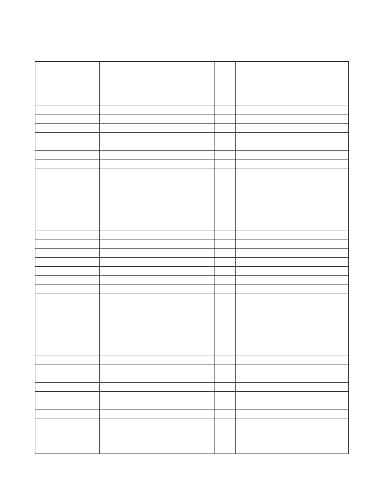
MICROCOMPUTER’S TERMINAL DESCRIPTION
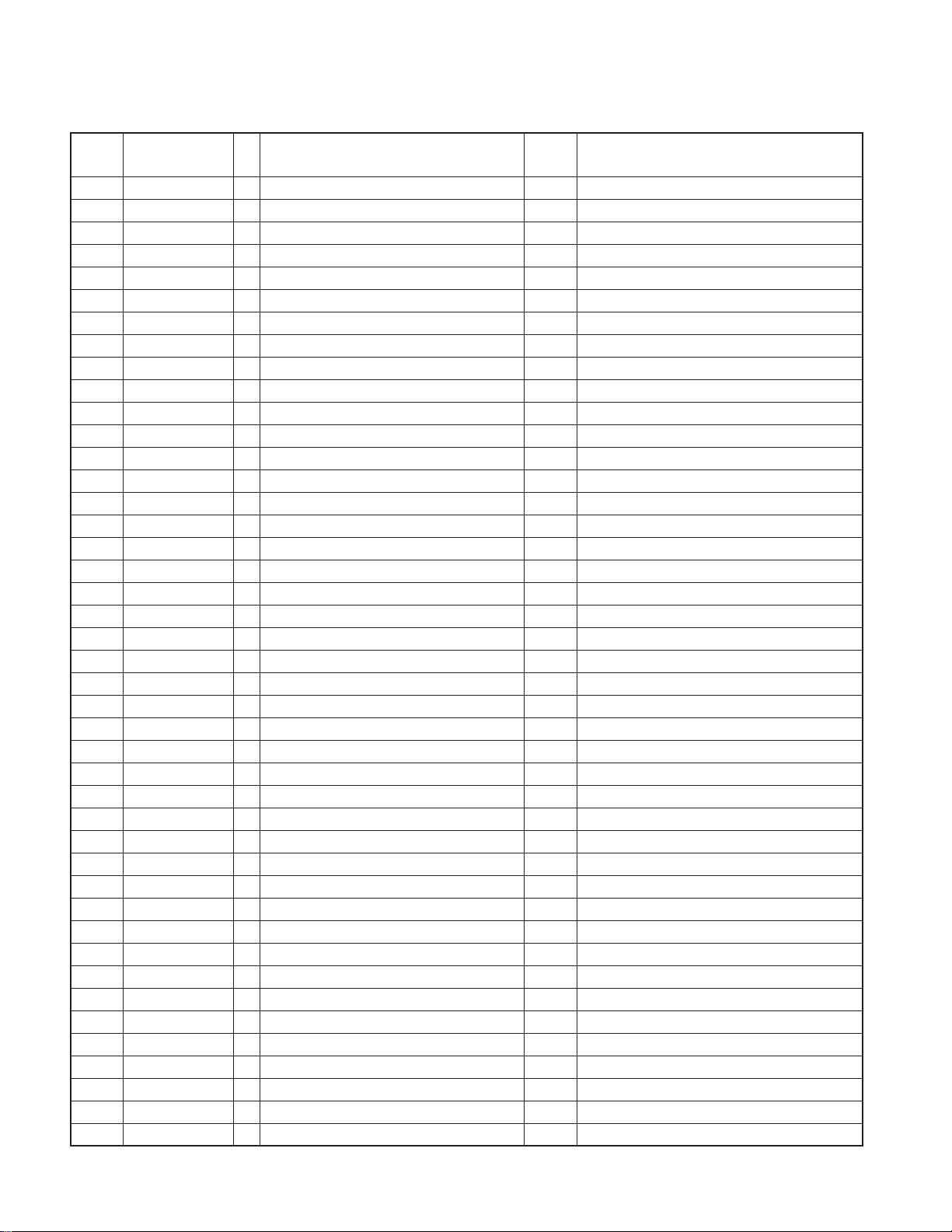
● SYSTEM MICROCOMPUTER: 703266YGJ504A (X34: IC304)
Pin No. Pin Name I/O Application
1AVREF0
2AVSS
3 VMUTE3 O MUTE to free-run timing controller H: When FULL OSD, L: When EXCEPT
4 VMUTE2 O Switching chroma input SYNC H: When FULL OSD, L: EXCEPT
5AVREF1
6 PWM O DIM_PWM output timing count Duty100%: Brightness MAX, 150Hz
7 HSY I Backlight (BRIGHT) brightness adjustment
8 FLMD0
9 VDD
10 REGC
11 VSS
12 X1
13 X2
14 RESET
15 XT1
16 XT2
17 OSD_RST O Reset to OSD-IC L: RESET
18 VSY I PWM output trigger
19 SRC I Source KEY detection L: SOURCE pressed
20 DRST O NC L fixed
21 OSD_CS O Chip select to OSD-IC
22~24 NC O NC LOW is fixed at L
25 DVS_SYS_DATA O Data output to DVS-7600
26 DVS_BE_DATA I Data input from DVS-7600
27 DVS_BE_CLK I Clock input from DVS-7600
28,29 NC O NC L fixed
30 REMO I Remote control data input
31 NC O NC L fixed
32 NC O NC L fixed
33 EVSS
34 EVDD
35
35
36
36
37 REG_F- O SWReg external sync Pulse output. Reversed phase of REG_F+
38 REG_F+ O SWReg external sync Pulse output
39 NC O NC L fixed
40 CRM_CS O Chroma IC control (RB5P0090)
S_SDA/
S_ROM_CORR data input/output address
S_SDA/E2P_SDA
S_SCL/
S_ROM_CORR clock output address
S_SCL/E2P_SCL
ROM correction E2PROM communication
I/O
O Chroma IC adjustment E2PROM control E2PROM communication
ROM correction E2PROM communication
O
O Chroma IC adjustment E2PROM control E2PROM communication
Truth
value table
r
r
Processing Operation Description
Normally: PMW CLK for control
Chroma adjustment mode: RGB timing detection
Please refer to the truth value table for slave
Please refer to the truth value table for slave
9
DDX6019/6029/6029Y/6039
MICROCOMPUTER’S TERMINAL DESCRIPTION
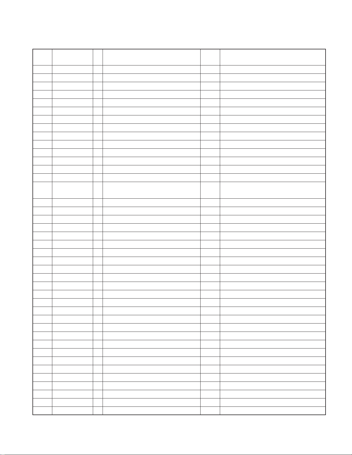
Pin No. Pin Name I/O Application
41 CRM_SDA O Chroma IC control (RB5P0090)
42 CRM_SCL O Chroma IC control (RB5P0090)
43~47 NC O NC L fixed
48 DAC_MUTE O MUTE control to audio µ-com H: MUTE OFF, L: MUTE ON
48 NC O NC LOW is fixed at L
49 NC O NC L fixed
50 OSD_DATA O Data to OSD-IC
51 OSD_CLK O Clock to OSD-IC
52~58 NC O NC L fixed
59 SYS_SREQ I AUDIO_COM communication request input
60~63 NC O NC L fixed
64 SYS_MUTE O When ACC_OFF, MUTE DRIVER control H: MUTE ON
65 A_PON I A_PON (Input from Audio)
66 SYS_ON O AUDIO_COM communication control output H: Start up request to AUDIO µ-com
67 SYS_MREQ O AUDIO_COM communication request output
68 SYS_SDATA I AUDIO_COM communication data input
69 SYS_MDATA O AUDIO_COM communication data output
70 SYS_M_CLK O AUDIO_COM communication clock output
71
72
73 S_FLASH_CLK I For flash writing ROM writer communication
74 BL DET O Not used (backlight error detection) LOW fixed
75 S_BU_DET I BU detection H: BU reduced voltage detection
76 NC O NC LOW is fixed at L
77 ACC_DET I ACC detection L: ACC ON detection
78 ILLUMI I ILL detection L: Illumi ON
79 PARKING I Parking detection H: Parking ON
80 REVERSE I Reverse detection L: Reverse ON
81 NC O NC L fixed
82 PON O Power supply control output H: PON
83 POWER_DET I Power supply error detection L: SW14V short
84 MCNT O
85~87 NC O NC L fixed
88 S_TYPE0 I Destination determination K,R,E,M,X,V q Refer to the truth value table
89 S_TYPE1 I Destination determination K,R,E,M,X,V q Refer to the truth value table
90 S_TYPE2 I Destination determination K,R,E,M,X,V q Refer to the truth value table
91 S_WRT_E2P I Used when writing E2P H: When writing E2PROM
92 JIG_EJ I Forced mechanism open H: Open (for assuring)
93,94 NC O NC L fixed
95 NC O NC Fixed at L when LOW
96 DISC_DET I Disc detection L: Disc IN
97 NC O NC L fixed (LOW)
98 DVS_BE_REQ I DVS-7600 communication request input
S_FLASH_MDATA
S_FLASH_SDATA
IFor flash writing ROM writer communication
OFor flash writing ROM writer communication
Motor driver voltage switching tilt mechanism 8V
Truth
value table
Processing Operation Description
H: Mechanism speed down
10
DDX6019/6029/6029Y/6039
MICROCOMPUTER’S TERMINAL DESCRIPTION
Pin No. Pin Name I/O Application
99 DVS_SYS_REQ O DVS-7600 communication request output
100 NC O NC L fixed (LOW)
101 DVS_BE_PON O DVS-7600 power supply control H: PON (LOW)
102 DVS_BE_RST O DVS-7600 reset
103 BVSS
104 BVDD
105 TILT_M+ O
106 TILT_M- O
107~109
110 FLMD1 NC L fixed
111~114
115 NC O NC L fixed
116 BL ENA O Backlight ON/OFF H: Backlight ON, L: Backlight OFF
117 MONI_SEL O Monitor output switching H: NAVI, TV (SECAM), L: EXCEPT
118 VMUTE1 O
119 HPOS3 O HPOSI switching for each video source e Refer to the truth value table
120 NT/PAL O Sync separation IC control L: NTSC, H: PAL
121 HPOS2 O HPOSI switching for each video source e Refer to the truth value table
122 MODE3 O Screen mode switching w Refer to the truth value table
123 HPOS1 O HPOSI switching for each video source e Refer to the truth value table
124 MODE1 O Screen mode switching w Refer to the truth value table
125 MODE2 O Screen mode switching w Refer to the truth value table
126 MIRROR O Mirror MODE switching H: Mirror, L: Normal
127 HPOS4 O HPOSI switching for each video source e Refer to the truth value table
128 X1 O Touch panel X axis standard voltage control
129 TL_DET I SW8V reduced voltage detection H: Reduced voltage detection
130 TILT_POS I Reversed tilt mechanism position detection
131 NC O NC Low: L fixed
132 VR I Video input when adjusting chroma IC
133 VG I Video input when adjusting chroma IC
134 VB I Video input when adjusting chroma IC
135 VCOM I VCOM input when adjusting chroma IC
136 X0 O Touch panel X axis GND control
137 Y0 O Touch panel Y axis GND control
138 X_DATA I Touch panel voltage detection X direction voltage detection
139 Y_DATA I Touch panel voltage detection Y direction voltage detection
140 KEY4 I Monitor panel KEY 4 individual detection VOL→ATT→FNC→VSEL (priority order)
141 VOL+ I Monitor panel VOL+ KEY individual detection L: VOL+ pressed
142 OPEN/CLOSE I OPEN/CLOSE KEY detection L: OPEN/CLOSE pressed
143 KEY_ILL O Monitor panel KEY illumi control H: Monitor KEY illumi ON
144 SI O Security indicator control L: OFF, H: ON
NC O NC LOW is fixed at L
NC O NC LOW is fixed at L
Reversed tilt mechanism motor control + CLOSE
Reversed tilt mechanism motor control - OPEN
When switching video source,
when V_OFF screen MUTE
Truth
value table
t Refer to the truth value table
t Refer to the truth value table
Processing Operation Description
H: MUTE ON
11
DDX6019/6029/6029Y/6039
MICROCOMPUTER’S TERMINAL DESCRIPTION
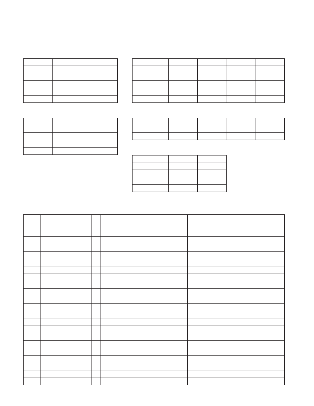
Truth value table
q Destination setting
Destination TYPE2 TYPE1 TYPE0
K001
E010
M011
V/X 1 0 0
R111
e Screen position
Monitor source HPOS1 HPOS2 HPOS3 HPOS4
FULL OSD 0 0 0 0
NTSC 0 1 0 0
PAL 0 0 1 0
SECAM 1 1 1 0
NAVI 0 1 0 0
w Screen mode
MODE MODE 1 MODE 2 MODE 3
FULL 0 0 0
NORMAL 1 0 0
WIDE 0 1 0
ZOOM 1 1 0
r E2PROM slave address
IC name Application A2 A1 A0
BR24C01AFV Normal use 0 0 0
BR24L02FV
t Reversed tilt motor driver
Mechanism operation
Stop 0 0
OPEN 0 1
CLOSE 1 0
Brake 1 1
ROM correction
TILT_M+ TILT_M+
110
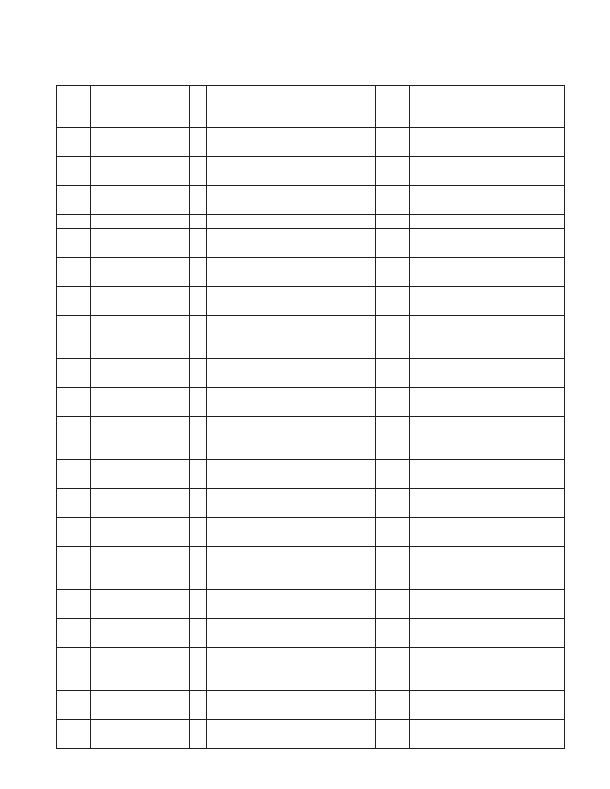
● AUDIO MICROCOMPUTER: 703030BYGCJ26 (X14: IC101)
Pin No. Pin Name I/O Application
1 TUN_TYPE0 I TUNER destination L fixed
2 TUN_SCL O F/E I2C clock output terminal
3NAV_RX I Navi control data input
4NAV_TX O Navi control data output
5 TUN_TYPE1 I TUNER destination L fixed
6 EVDD
7 EVSS
8 EXT_CON O EXT-CONT output
9NC O L fixed
10 VSYNC_DET I Video detection, NTSC/PAL determination NTSC: 50Hz, PAL: 60Hz
11 NC O L fixed
12 SYS_MDATA I SYS_COM communication data output
13 SYS_SDATA O SYS_COM communication data input
14 SYS_MCLK I SYS_COM communication clock input
15 NC O L fixed
16 AUTO_SW_2 O Video detection, NTSC/PAL determination
17 BEEP O BEEP When BEEP: Pulse output
18 IC/VPP
19 AUTO_SW O Video detection, NTSC/PAL determination H: AVIN, L: BACK CAMERA
20 TV_MC_REQ O Communication request to TV_COM
Truth
value table
Processing Operation Description
H: When AVIN2 (to ensure a port)
In practice, fixed to L (AVIN/BACK CAM)
12
DDX6019/6029/6029Y/6039
MICROCOMPUTER’S TERMINAL DESCRIPTION
Pin No. Pin Name I/O Application
21 TV_SC_CON O Start-up request to TV_COM
22 TV_JUDGE I TV-BOX new/old detection
23 VOUT_MUTE3 O V. OUT MUTE e Refer to the truth value table
24 VOUT_SEL1 O V. OUT selector (BA7649) e Refer to the truth value table
25 VOUT_SEL2 O V. OUT selector (BA7649) e Refer to the truth value table
26 VSEL1 O V. IN selector (BA7649) w Refer to the truth value table
27 VSEL2 O V. IN selector (BA7649) w Refer to the truth value table
28 VSEL3 O V. IN selector (BA7649) w Refer to the truth value table
29 RGB_MUTE O MUTE RGB except when NAVI or SECAM w Refer to the truth value table
30 RGB_SW O Switch NAVI/SECAM w Refer to the truth value table
31 RESET
32 XT1
33 XT2
34 REGC
35 X2
36 X1
37 VSS
38 VDD
39 CLKOUT
40 NC O L fixed
41 PWIC_STBY O PWIC standby H: POWER ON, L: POWER OFF
42 PWIC_MUTE O PWIC_FR MUTE L: MUTE ON
43 P_CON O P-CON control output
44 ANT_CON O P-ANT control output H: ANT UP, L: ANT DOWN
45 AM+B O AM power supply ON H: When AM, L: EXCEPT
46 PRE_MUTESW O PREout sub woofer MUTE H: MUTE OFF, L: MUTE ON
47 PRE_MUTER O PREout rear MUTE H: MUTE OFF, L: MUTE ON
48 PRE_MUTEF O PREout front MUTE H: MUTE OFF, L: MUTE ON
49 SYS_MREQ I SYS_COM communication request output
50 SYS_SREQ O Communication request to SYS_COM
51 LX_CON/LX_CON O Start-up request to slave unit
52 LX_REQ_M/LX_REQ_M O Communication request to the slave unit
53 LX_RST/LX_RST O Hardware-reset to slave unit
54 LX_MUTE/LX_MUTE I MUTE request from slave unit
55 BVDD
56 BVSS
57 AIN_SEL1 O For ASEL (LOW only) r Refer to the truth value table
58 AIN_SEL2 O For ASEL (LOW only) r Refer to the truth value table
59 AIN_SEL3 O For ASEL (LOW only) r Refer to the truth value table
60 AIN_SEL4 O For ASEL (LOW only) r Refer to the truth value table
61 AUD_MUTE0 O E-VOL front MUTE L: MUTE ON, H: MUTE OFF
62 AUD_MUTE1 O E-VOL rear MUTE L: MUTE ON, H: MUTE OFF
63 AUD_MUTE2 O E-VOL center, SWMUTE L: MUTE ON, H: MUTE OFF
Truth
value table
Processing Operation Description
L: When STANDBY or POWER OFF
H: EXCEPT
13
DDX6019/6029/6029Y/6039
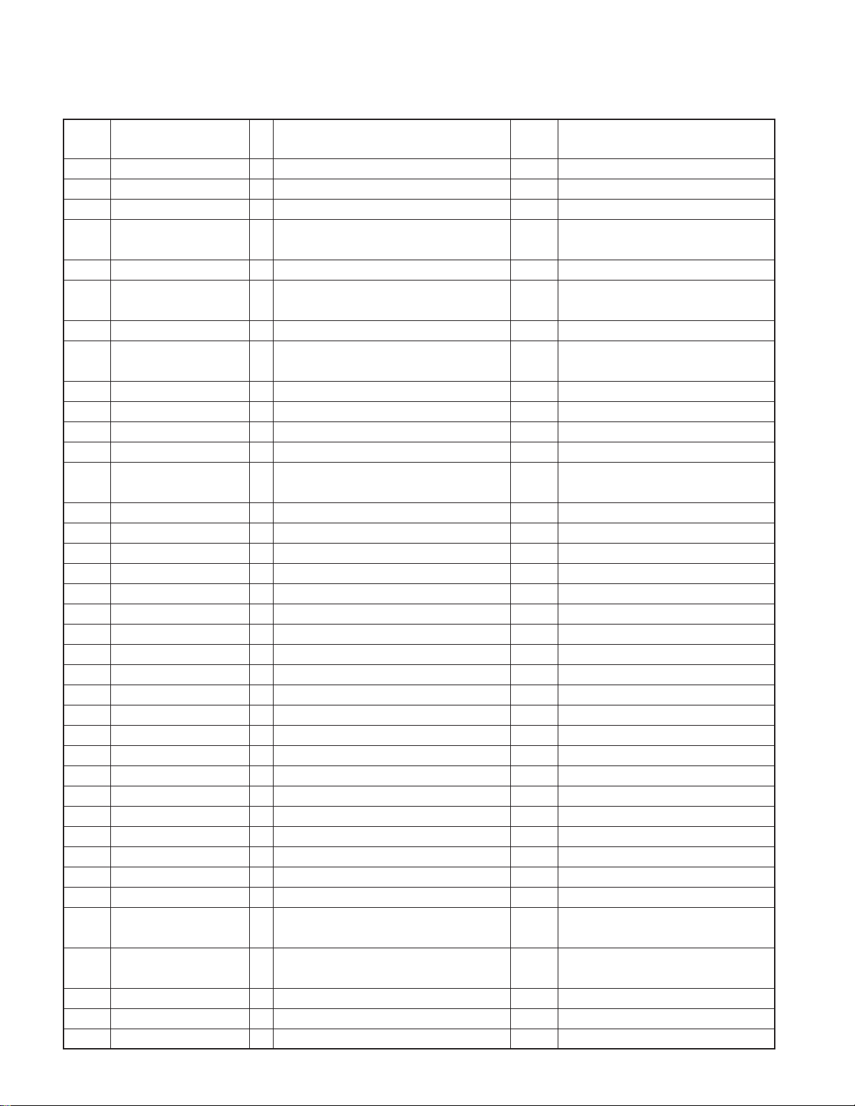
MICROCOMPUTER’S TERMINAL DESCRIPTION
Pin No. Pin Name I/O Application
64 AUD_MUTEA O E-VOL inputSEL_A MUTE L: MUTE ON, H: MUTE OFF
65 AUD_MUTEB O E-VOL inputSEL_B MUTE L: MUTE ON, H: MUTE OFF
66 AUD_MUTEC O E-VOL inputSEL_C MUTE L: MUTE ON, H: MUTE OFF
67
67 AUD_SDA/AUD_SDA I/O E-VOL data output
68
68 AUD_SCL/AUD_SCL O E-VOL clock output
69 A_PON O SW5V ON/OFF
70 NC O NC L fix ed
71 AVDD
72 AVSS
73 AVREF
74 LINE_MUTE I LINE-MUTE input detection
75 A_WRT_E2P I Used when writing E2PROM H: When writing E2PROM
76 A_TYPE0 I Destination determination q Refer to the truth value table
77 A_TYPE1 I Destination determination q Refer to the truth value table
78 A_TYPE2 I Destination determination q Refer to the truth value table
79 A_TYPE3 I Destination determination q Refer to the truth value table
80 PWIC_DCDET I SP_FR output DC offset detection L: When detected
81 TUN_SMET I S meter input
82 TUN_IFC I F/E IFC OUT input terminal H: Station found, L: Station not found
83 R_QUAL I RDS decoder QUAL input terminal
84 R_DATA I RDS decoder DATA input terminal
85 R_NOISE I FM noise detection terminal
86 R_AFS_H/R_AFS_H I/O Switching constant when noise detected
87 R_CLK/R_CLK I RDS decoder CLK input terminal
88 A_BU_DET I BU reduced voltage detection H: Reduced voltage detection
89 SYS_ON I SYS_COM communication control input H: Start up request from AUDIO µ-com
90 TV_SC_REQ I Communication request from TV_COM
91 M_MUTE I MUTE request from system µ-com L: MUTE request
92 LX_REQ_S/LX_REQ_S I Communication request from slave unit
92 LX_REQ_S/NC O Fixed to L only when CH
93 NC O L fixed
94
95
96
97
98
AUD_SDA/
A_RCORR_SDA data input/output
AUD_SCL/
A_RCORR_SCL clock input/output
TV_SC_DATA/
TV_SC_DATA
TV_MC_DATA/
S_TV_MC_DATA
TV_BP_CLK/TV_BP_CLK
LX_DATA_S/LX_DATA_M
LX_DATA_M/LX_DATA_M
ROM correction E2PROM communication
I/O
ROM correction E2PROM communication
O
IDATA input from TV_COM
ODATA output to TV_COM
O CLK output to TV_COM
I Data from slave unit
O Data to slave unit
Truth
value table
Processing Operation Description
H: Output only when in RESET sequence
L: Other output
Normal: 1.6V, TEL MUTE: 1V or lower,
NAVI MUTE: 2.5V or higher
14
DDX6019/6029/6029Y/6039
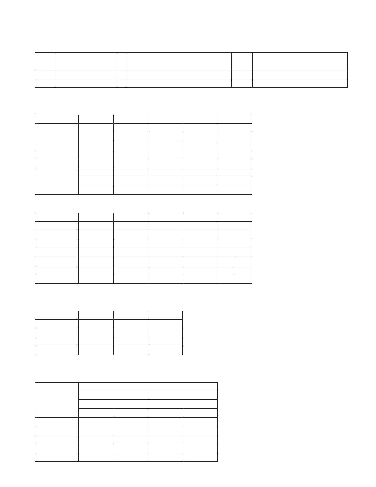
MICROCOMPUTER’S TERMINAL DESCRIPTION
Pin No. Pin Name I/O Application
99 LX_CLK/LX_CLK O LX BUS clock
100 TUN_SDA I/O F/E I2C data input/output terminal
Truth
value table
Truth value table
q Destination setting
Model Destination TYPE3 TYPE2 TYPE1 TYPE0
M0011
DDX-CH V/X 0 1 0 0
X0101
DDX6019 K 1 0 0 1
DDX6029/6029Y E 1 0 1 0
M1011
DDX6039 V/X 1 1 0 0
R1111
w AV selector control 1
Monitor source VSEL1 VSEL2 VSEL3 RGB_SW RGB_MUTE
TV (NTSC, PAL) 0 0 0 0 0
AVIN 0 1 000
DVD 1 0000
R CAMERA 1 1 0 0 0
NAVI ∗∗1111
TV (SECAM) 0 0 0 0 0 1
FULL OSD ∗∗∗00
∗: Don’t care
Processing Operation Description
e AV selector control 2
AV OUT source VOUT_SEL1 VOUT_SEL2
DVD 0 1 0
AVIN 1 0 0
TV 0 0 0
OFF ∗∗1
∗: Don’t care
r AV selector control 3: IC201 (IC2-6) input
IC203 IC202
MAIN SUB
ABAB
Monitor source AIN_SEL_1 AIN_SEL_2 AIN_SEL_3 AIN_SEL_4
TV 1 1 11
LX 0 1 ∗∗
AVIN2 (Not used) 1 0 1 0
AVIN1 0 0 0 0
∗: Don’t care (no LX on SUB)
VOUT_MUTE3
TC4052BFT
15
DDX6019/6029/6029Y/6039
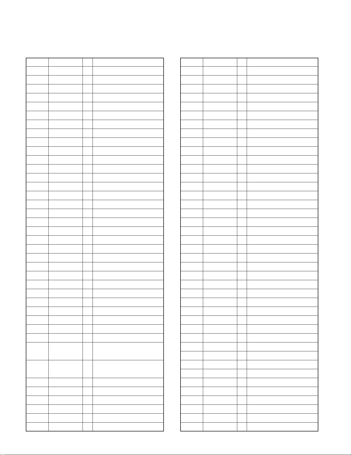
MICROCOMPUTER’S TERMINAL DESCRIPTION
● DISC CONTROLLER MICROCOMPUTER: MN103S71F (X37: IC4)
Pin No. Pin Name I/O Application
1 SW_2 I
2 SW_3 I Lo-START detection
3 CDON O CD-LD ON
4 VDD3 - VDD (3.3V)
5 VSS - VSS
6FGIMotor FG input
7 SW_4 I Lo-END detection
8,9 FADR17,18 O Address output to FLASH
10 FADR11 O Address output to FLASH
11 FADR9 O Address output to FLASH
12 VDD15 - VDD (1.5V)
13 FADR8 O Address output to FLASH
14,15 FADR13,14 O Address output to FLASH
16 NWE O Right signal output to FLASH
17,18 FADR16,15 O Address output to FLASH
19 DRAMVDD15 - DRAM power supply (1.5V)
20 DRAMVSS - VSS for DRAM
21 VSS - VSS
22 FADR12 O Address output to FLASH
23~30 FADR7~0 O Address output to FLASH
31 VSS - VSS
32 VDD3 - VDD (3.3V)
33~40 FDT0~7 I/O Data input/output with FLASH
41 NCE O
42 FADR10 O Address output to FLASH
43 NOE O Read signal output to FLASH
44 MMOD I Test mode switching signal
45 NRST I Reset input
46 VSS - VSS
47 SCLOCK I/O Dwire clock terminal
48 SDATA I/O Dwire data terminal
49 TxD/EXTRG0 I/O
50 RxD/EXTRG1 I/O
51 VDD3 - VDD (3.3V)
52 OSCI I
53 OSCO O
54 VSS - VSS
55 OFS_TE O CD TE offset cancel output
56 DRV1 O Drive output for spindle drive
8cm Ej-STOP, Lo-START detection
Chip select signal output to FLASH
Serial transmission/
Dwire trigger terminal
Serial reception/
Dwire trigger terminal
Oscillation input (16.897849MHz)
Oscillation output (16.897849MHz)
Pin No. Pin Name I/O Application
57 DRV2 O
58 DVDON O DVD-LD ON
59 STEP_A O Thread control output A
60 STEP_B O Thread control output B
61 Lo/Ej O Lo/Ej control terminal
62 LO.MUTE O Lo/Ej mute terminal
63 VSS - VSS
64 DRV.MUTE O Driver mute control
65 BMS O Spindle short brake control
66 LIM-SW I LIM-SW detection
67 Gain_SW O PDIC Gain switching
68 FEPCK O FEP clock output
69 FEPDT O FEP data output
70 FEPEN O FEP enable signal
71 DRAMVSS - VSS for DRAM
72 DRAMVDD15 - DRAM power supply (1.5V)
73 DRAMVDD33 - DRAM power supply (3.3V)
74 VDD3 - VDD (3.3V)
75 FG I Motor FG input
76 TX O Output for digital OUT
77 VDD15 - VDD (1.5V)
78 VSS - VSS
79 TSTSG O EQ calibration signal
80 VFOSHORT O Not used.
81 JLINE O J-line setting output
82 BDO I Dropout signal input
83 OFTR I Off-track signal input
84 AVSSD - VSS for analog
85 ROUT O MASH Rch audio output
86 LOUT O MASH Lch audio output
87 AVDDD - VDD (3.3V) for analog
88 VCOF I JFVCO control voltage
89 TRCRS I
90 AVDDC - VDD (3.3V) for analog
91 WBLIN I WBL input
92 CSLFLT I Not used
93 RFDIF I Not used
94 AVSSC - VSS for analog
95 PLFLT2 I Condenser 2 for PLL
96 PLFLT1 I Condenser 1 for PLL
97 AVSSB - VSS for analog
Focus balance adjustment output
Track loss generation signal input
16
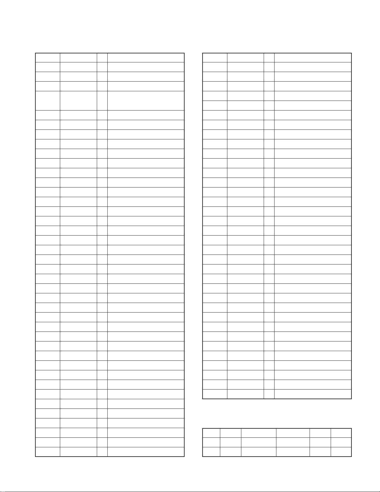
DDX6019/6029/6029Y/6039
MICROCOMPUTER’S TERMINAL DESCRIPTION
Pin No. Pin Name I/O Application
98 ARF I Equivalent RF+ input
99 NARF I Equivalent RF- input
100 VHALF I Reference voltage 1.65V input
101 RV1 I
102 VREFH I Reference voltage 2.2V input
103 DSLF2 I Condenser 2 for DSL
104 DSLF1 I Condenser 1 for DSL
105 AVDDB - VDD (3.3V) for analog
106 JITOUT O For jitter monitor
107 AVDDA - VDD (3.3V) for analog
108 TECAPA I Not used
109 AD0 (FE) I FE input
110 AD2 (AS) I AS input
111 AD1 (TE) I TEph/TE3b input
112 AD3 (ENV) I RF envelop input
113
114 AD5 I Focus drive AD input
115 AD6 I Tracking drive AD input
116 AD7 (IOP) I
117
118 AVSSA - VSS for analog
119 PWM0 (FOD) O Focus drive output
120 PWM1 (TRD) O Tracking drive output
121 VSS - VSS
122 VDD3 - VDD (3.3V)
123 IDGT O Not used
124 DTRD O Not used
125 MONI0 O Internal monitor signal
126~130
131 SW_2∗3I
132 SW_1∗5I12cm Ej-STOP detection
133 DMARQ O DMA request output ATAPI host
134 NIOWR I ATAPI host write signal input
135 VDD3 - VDD (3.3V)
136 VSS - VSS
137 NIORD I ATAPI host read signal input
138 IORDY O Ready output to ATAPI host
139 NDMACK I
140 INTRQ O Interruption output to ATAPI host
141 NIOCS16 O Not used
AD4 (RFDIFO)
AD8 (TEMP_DET)
MONI1~5 O Internal monitor signal
VREFH register for reference
current power supply
I Push-pull TE input
Laser diode current measurement
ITemperature monitoring input
8cm Ej-STOP, Lo-START detection
ATAPI host DMA acknowledge input
Pin No. Pin Name I/O Application
142 DA1 I ATAPI host address signal input
143 NPDIAG I
144 DA0 I ATAPI host address signal input
145 VSS - VSS
146 VDD3 - VDD (3.3V)
147 DA2 I ATAPI host address signal input
148 NCS1FX I
149 NCS3FX I
150 NDASP O ATAPI drive active/slave
151 HDD15 I/O ATAPI data input/output
152 HDD0 I/O ATAPI data input/output
153 HDD14 I/O ATAPI data input/output
154 HDD1 I/O ATAPI data input/output
155 HDD13 I/O ATAPI data input/output
156 VDD3 - VDD (3.3V)
157 VDD15 - VDD (1.5V)
158 VSS - VSS
159 HDD2 I/O ATAPI data input/output
160 HDD12 I/O ATAPI data input/output
161 HDD3 I/O ATAPI data input/output
162 HDD11 I/O ATAPI data input/output
163 HDD4 I/O ATAPI data input/output
164 HDD10 I/O ATAPI data input/output
165 HDD5 I/O ATAPI data input/output
166 VSS - VSS
167 VDD3 - VDD (3.3V)
168 HDD9 I/O ATAPI data input/output
169 HDD6 I/O ATAPI data input/output
170 HDD8 I/O ATAPI data input/output
171 HDD7 I/O ATAPI data input/output
172 VDDH - 5V reference power supply
173 NRESET I ATAPI reset signal input
174 MASTER I ATAPI master/slave signal input
175 SCL O EEPROM clock output
176 SDA I/O EEPROM data input/output
Diagnosis from ATAPI slave to master
ATAPI host chip select signal input
ATAPI host chip select signal input
Loading/Eject logic
Pin No.
Name Hi-Z (MUTE) Short-Brake CW CCW
62 DRV7 H L L L
61 DRV6 1.65 (Hi-z) 1.65 (Hi-z) 3.3 (Hi) 0 (Low)
17

DDX6019/6029/6029Y/6039
TEST MODE
Operation Specifications
● How to enter the test mode
There are following 2 ways to enter the test mode:
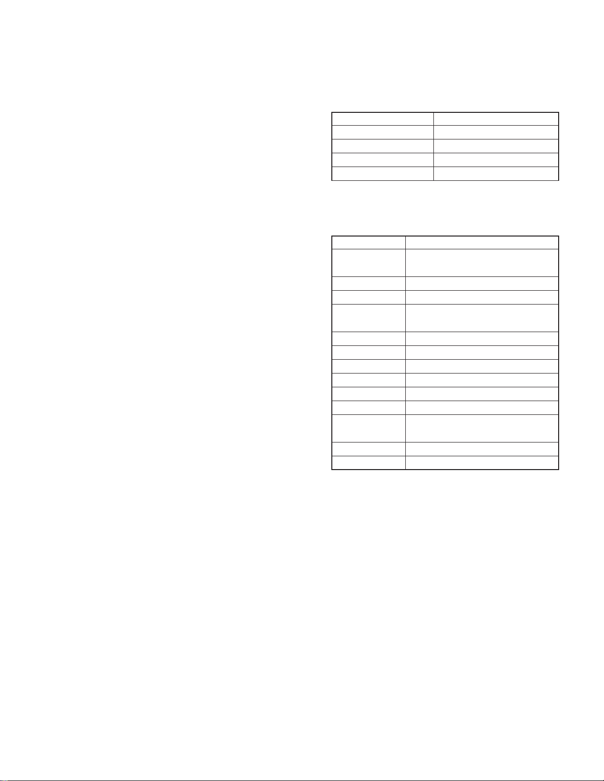
1. Press and hold the [SRC] and [ATT] keys and reset.
2. Connect region writing jig to Lx connector (when adjusting
flicker)
Notes:
Setting of the jig is optional. Ho we v er, note that the jig functions as setting SW (region/serial/security/CPPM).
Test mode is powered off in 30 minutes (to make it possib le
to operate without entering Security while Security ON).
While the jig is connected (after connection is recognized),
Key illumi blinks (flicker adjustment mode).
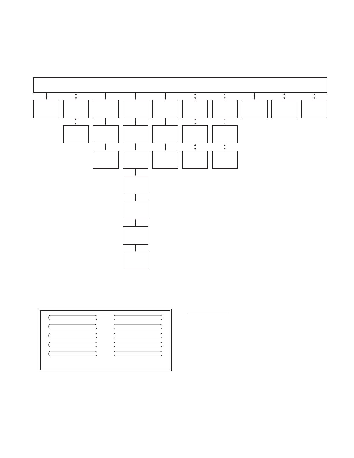
● Screen transition
By pressing each key on the Test Mode Main screen, move on
to the corresponding screen.
Test Mode Main Screen
Test Mode Main
Information
Service
Touch
Hposi
MECHA ADJ
● Information screen
Below is the contents displayed on the information screen.
• Serial No.
•Security Info (BLANK: Not written in E2PROM, ON/OFF:
Normal status (ON/OFF is security setting status), ERROR:
E2PROM writing error)
• DC Offset detection information
• System µ-Com Version / Rom Correction Version / Type
•Audio µ-Com Version / Rom Correction V ersion / Type / Span
(Tuner frequency span information)
• OSD Version
• Region Code
• B/E Version / F/E Version / Macrovision Version
• Tv Box Version / Rom Correction Version / Type
(Displayed only when Tv Tuner Box is connected. When the
previous model Tvtuner is connected, “– – – –” is displayed.)
Source
Set Up
Audio
Chroma Auto 1
Chroma Func
● TOUCH screen
• After Touch Position Control, save the memory into the
E2PROM.
• By 3 points input, memory from the system computer to
EEPROM
• E2PROM normal write or abnormal result will display on
the screen.
● HPOSI screen
• After Screen Position Adjustment, save the memory into
the E2PROM.
Adjust in the following order. Graphic → DVD → TV →
VIDEO → NAVI
• DVD wallpaper shall be fixed to NTSC.
• E2PROM normal write or abnormal result will display on
the screen.
• When adjusting DVD, TDV-540A (Title 3-Chapter 16) shall
be played.
After Disc Loading, press the remote control Tenkey 4 to
move on to Title 3-Chapter 16.
● SERVICE screen
• Below is the contents displayed on the service screen.
Power On time
DVD Play time (CD-DA/VCD/DVD-VIDEO/other) / Number
of DVD Eject times
DVD Mecha Error information
Dvd Mecha/Read/Hot Error: Detect/None
Dvd Other Error: Last Time (**h)
Dvd Other Error: Time Before Last (**h)
Number of Monitor Open times / Number of Monitor Close
times
E2PROM Chroma data information
DC Offset detection information
• Write Serial No.
By pressing the [Serial] key, the screen moves on to the
Serial No. input screen.
• E2PROM Chroma data clear
By pressing the [Clear] key, E2PROM’s Chroma data is
cleared.
• DC Offset data clear
By pressing the [Clear] key, E2PROM’s DC offset data is
cleared.
18
DDX6019/6029/6029Y/6039
TEST MODE
● Chroma Auto 1 screen
• After the auto adjustment for Chroma, save the memory
into the E2PROM.
Auto Adjustment items: RGB_Amplitude → Bright →
Ganma1 → Ganma2 → CONT_RGB2 → SUB_Bright_R
→ SUB_B right_B → COM_Amplitude
• E2PROM normal write or abnormal result will display on
the screen.
• EEPROM’ s Chroma data is not cleared b y writing region in.
EEPROM Chroma data is cleared by the [Clear] ke y on the
Service screen.
● Chroma Func screen
• After the Chroma adjustment, save the memory into the
E2PROM.
• Setting operation is done by the remote control.
• Chroma_IC adjustment screen (Item setup) → Write to
EEPROM
Setup items: Tint adjustment (00h~FFh)
Phase adjustment (00h~3Fh)
• E2PROM normal write or abnormal result will display on
the screen.
• EEPROM’ s Chroma data is not cleared b y writing region in.
EEPROM Chroma data is cleared by the [Clear] ke y on the
Service screen.
● MECHA ADJ screen
• After the panel mechanism position control, save the
memory into the E2PROM.
•Write the voltage value at when Full Open/Full Close into
E2PROM.
• E2PROM normal write or abnormal result will display on
the screen.
• In one of the conditions below , “NG” is displa y ed (when NG,
not written into E2PROM).
E2PROM writing-in error.
NG if the voltage acquiring value is 0.177V or higher when
Open.
NG if the voltage acquiring value is lower than 2.746V or
higher than 2.888V when Close.
● Source / Audio / Set Up screen
• Source / Audio Control / Set Up screens are same as when
in normal mode.
● Display
• Basically, dedicated screen when in Test Mode.
• Display Touch position (+). Howe v er, shall not be displayed
in Touch Adjust screen (under adjustment).
● Key
• [Tact] key specification is shown below.
Key Function
SRC/Vol Up/Vol Dw/Open (Eject)
ATTDriver for motor On
V.SEL
FNC As usual (no easy)
As usual
V.SEL+AVOUT (engaged with V.SEL)
● Remote control
• Carry out the following operations using NA-R300 (SW:
AUD) (other than the listed b low shall be operated normally).
Key code Item
Direct Chroma_IC adjustment mode ON/OFF
(writing-in)
Band (FM+) Video mode switching (NAVI/AVIN/DVD)
M/S (AM-) DVD audio/video confirmation switching
Execution Setup/cancel Chroma setting value
(Play/Pause)
Tenkey 5 Navi forced interruption
Tenkey 6 Call Screen adjustment screen
Tenkey 7 To the item before Chroma adjustment
Tenkey 8 Change the Chroma setup value (UP)
Tenkey 9 To the next Chroma adjustment item
Tenkey 0 Change the Chroma setup value (DW)
Tenkey 2 (Preset 2)
Tenkey 3 (Preset 3)
Tenkey 4 (Preset 4)
DC Offset detection test direct switching
(DVD source only)
Switching the V-IN (R-CAM) mirror mode
Direct switching for HPOSI DVD checking
● Screen maintenance section
• In Test Mode (including when the jig is connected), start up
in VIDEO screen → press the [FNC] k e y to move on to Test
Mode Main screen.
• Connect AVOUT to the V.SEL action to allow change
(AVOUT when in Graphic and NAVI can be any).
AVIN – (TV) – R_CAM – NAVI – D VD (the order can be any)
• Easy Control screen is skipped with [FNC] key.
• For the Reverse condition needs to be set ON when in the
test mode (RCAM is always available in V.SEL).
(When detecting Reverse, R-CAM interruption will occur as
is in normal mode).
• When VIDEO image is input and when video signal is
switched (NTSC ↔ PAL), OSD is not displayed. (OSD is
displayed when s witching V.SEL. However, the OSD is not
displayed in VIDEO mode.)
19
DDX6019/6029/6029Y/6039
TEST MODE
● Audio
• Default volume is Step 30.
• Bal/Fad setting is changed among Min ↔ Center ↔ Max by
each click.
• Line Mute default is On.
•Xover setting is changed between Min ↔ Max by each click.
•Tone setting is changed among Min ↔ Center ↔ Max by
each click.
• Default Tone (EQ) value is Flat.
• Default system Q is OFF.
• When there is Digital Out terminal, the setting should always be output on setting.
• Sub Woofer default is ON (same in the normal mode).
● Tuner
• When unable to access E2PROM, display “Error” (Tuner
screen).
• K3I forced switching among narrow/middle/wide.
Forced to narrow by pressing and holding Preset 4
: “∗∗∗.∗1MHz”
Forced to middle by pressing and holding Preset 5
: “∗∗∗.∗2MHz”
Forced to wide by pressing and holding Preset 6
: “∗∗∗.∗3MHz”
• Switch Tuner Span (K ↔ M) with [SRC] key + [V ol. Dw] key
+ Reset.
Span information is displayed on the Information screen.
● BEEP control
• Beep regardless of the destination.
(While in Standby source, beep cannot be output because
of PWIC restriction.)
● SI control
• Set SI default to On.
● AVIF
• AVIN Interruption default shall be On.
• NAVI interruption SP setting default is FRONT ALL.
•V-IN mirror mode switching is done by Remote Control
Tenkey 3.
• R-CAM Interruption default shall be On.
● SCREEN adjustment
• By pressing the remote control Tenkey 6 on each video
screen, each video screen’s SCREEN adjustment items are
displayed.
• The default is Center , and s witch among Full Do wn ↔ Center ↔ Full Up by each click.
• BRT default is MAX.
● TV tuner
• If the destination is E, set the TV2 default value to “Area 5
(Russia)”, “Ch 8 (191.25MHz)”. (When KTC-V500 is connected.)
• If the destination is E, set the TV2 default value to “Area 4
(Russia)”, “Ch 8 (191.25MHz)”. (When KTC-V300 is connected.)
(HPOSI adjustment mode shall be TV1.)
* If started up as above, even if the test mode is cancelled b y
ACC/Power OFF → ON, the setting values are maintained
(set to default by Reset).
● DVD
• CD media KTD-02A and DVD media TDV-540A/TTD-100
are used.
• If the test mode is started up with Disc loaded Panel Open
and in test mode, the disc is not ejected (same in normal
mode).
• Set region code at the position for the time code.
• When Loading, set to Title1-Chapter1 (Shown with ★ in the
table below)
• CDDA audio checking (KTD-02A)
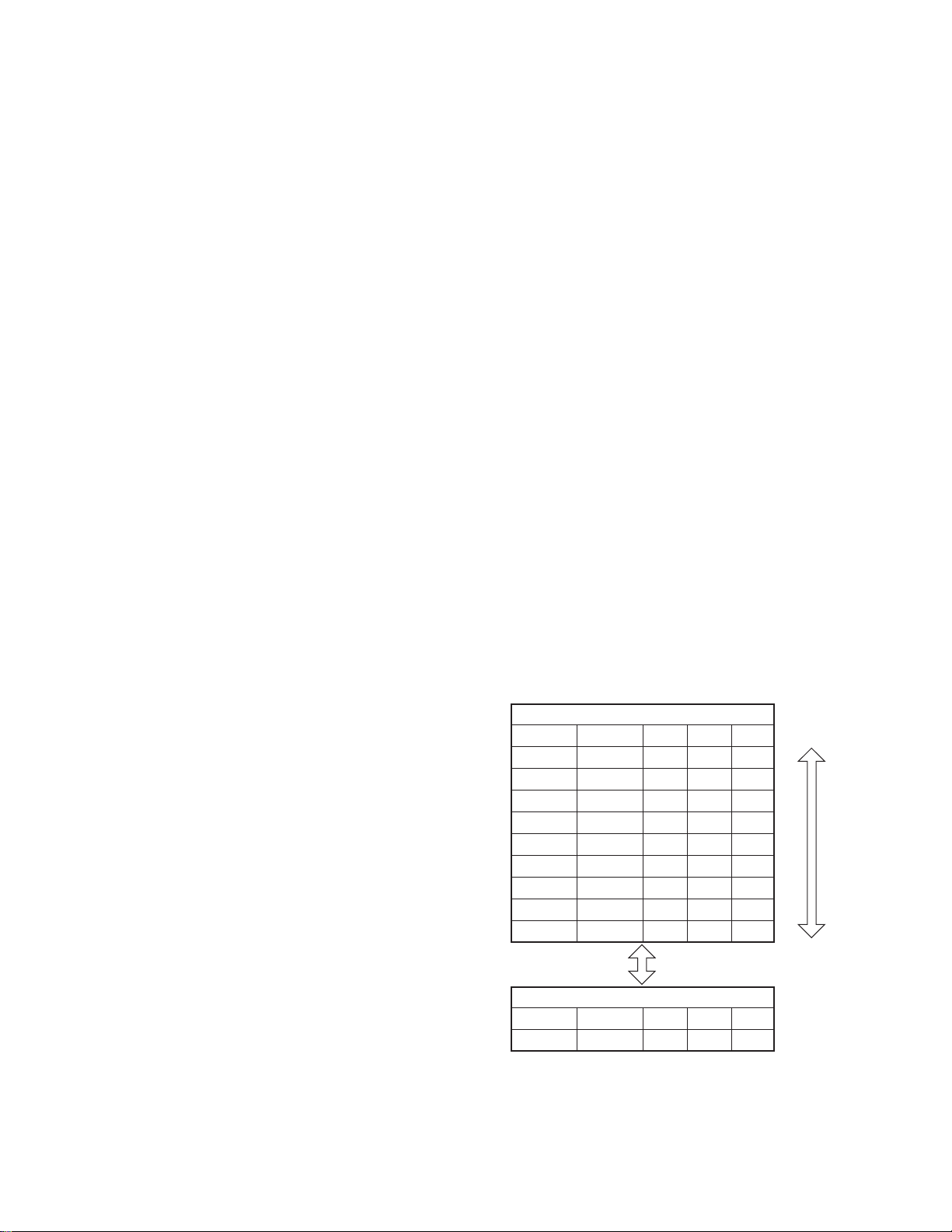
For CDDA audio checking
Track
★ 1-
915 10 11 12 13 14 -
9-
RDM
For CDDA audio checking
Track
28 -
Track
Up/Dw
20
DDX6019/6029/6029Y/6039
TEST MODE
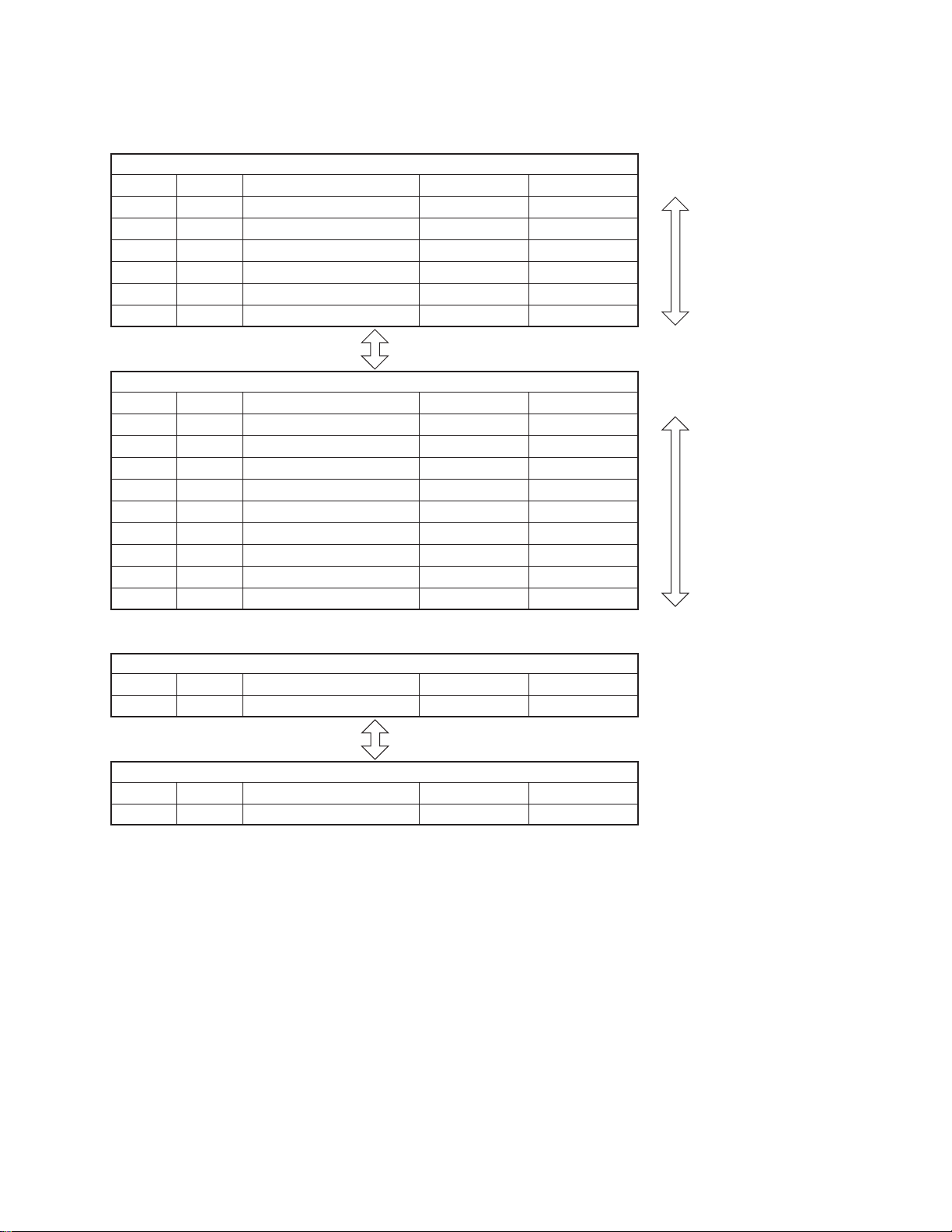
• DVD audio/video checking (TDV-540A)
For DVD video checking
Title Chapter
★ 11 AudioStream1
36Level AudioStream1
37S/N AudioStream1
317AM/PM noise AudioStream1
38Frequency characteristics AudioStream1
312Color bar measurement AudioStream1
DISC DW (M/S)
For DVD audio checking
Title Chapter
11 AudioStream1
411kHz 0dB PCM96k/24bit AudioStream3
4617Hz PCM96k/24bit AudioStream3
41644kHz PCM96k/24bit AudioStream3
42infinity PCM96k/24bit AudioStream3
43L PCM96k/24bi AudioStream3
44R PCM96k/24bit AudioStream3
411kHz 0dB Dolby AudioStream1
42infinity Dolby AudioStream1
Chapter
Up/Dw
Chapter
Up/Dw
• HPOSI video adjustment (TDV-540A)
For DVD video HPOSI checking
Title Chapter
★ 11 AudioStream1
TenKey 4 (Preset 4)
For DVD video HPOSI checking
Title Chapter
316Monoscope AudioStream1
● Flicker adjustment
Specification is as shown below (jig is connected to Lx or Tv).
1. Connect the jig to Lx or Tv and turn on the power to set
flicker adjustment to On.
The panel mechanism tilt position is started up as “2”.
Note: Setting of the jig is optional. However, note that the
jig functions as setting SW (region/serial/security/CPPM).
2. Screen mode is set to ZOOM and the screen shown is
VIDEO.
3. By turning the power off, flicker adjustment is set to Off.
● DC Offset
• DC Offset detection status (normal/error) clear.
By the Service information screen’s DC Offset information
[Clear] key, clear E2PROM’s DC Offset detection information.
• DC Offset detection information is displayed on the Information screen/Service information screen.
• While in the test mode, even if DC Offset is detected, it is
not written into E2PROM. → Even in the test mode, when
DC is detected, “Protect” is displayed (all CH Mute) as in
normal mode.
21

DDX6019/6029/6029Y/6039
TEST MODE
•Volume setting is changed to the setting values below by
pressing the remote control Tenkey 2 (Preset 2).
Source: DVD
Specified disc: KTD-02A
Specified Track: 15 (20Hz, 0dB)
DISC/TRACK shall be specified by hand.
Specified Vol: 29
• If Lx is connected, even if DC Offset is detected in the test
mode, LxCon should not be Off.
● Specification to set the driver for motor without
the slide mechanism
• With the condition when [ATT] key is pressed and hold, the
driver port for motor shall be On.
With the [ATT] key pressed and hold, and with the key on
once, the motor is ON to the reversed direction, and stopped
by key OFF.
By 2nd time key On, the motor is ON to the forward direction, stopped by key OFF, and then repeated thereafter.
● Backup Memory
• While in the test mode, the Backup Memory function (save
to the memory 30 mimutes after reset and then every 1
hour thereafter) is not active.
● E2PROM contents clear
• Clear the E2PROM contents which should not remain when
shipped.
If information clearing and mechanism initialization fail with
the following procedure, do not light the illumi for SI.
Clear with [SRC] key + [FNC] key + Reset.
DC Offset information
Retailer mode information
Memory function
Service Information
• If a jig is connected and the region is written in, the following contents should be cleared.
Serial No.
DC Offset information
Security code
Memory function
Touch correction
Retailer mode information
HPOSI data
Service Information
Mechanism position adjustment value
● Other
• Operate Illumi/Parking operation even if in the test mode
(same as when in normal mode).
(Input from extended connector shall be valid.)
• R-CAM Interruption default shall be On.
•Even in the status where the panel mechanism is Full Open,
Touch operation shall be available.
● About the retailer mode
• Retailer mode is turned On by [Eject] key + [Vol. Dw] + Reset.
• Retailer mode is turned Off by [SRC] key + Reset.
• Retailer mode ON/OFF status shall be saved into E2PR OM
memory.
• When started up in the retailer mode, both audio and video
start up as DVD source.
• While in the retailer mode, to prevent the disc to be stolen,
the [Eject] key shall be pressed and hold f or 10 seconds to
eject.
22
TEST MODE
Test Mode Screen Specifications
• If Graphic screen is displayed while in the test mode, the
test mode main screen is displayed.
Test Mode Main screen
DDX6019/6029/6029Y/6039
Information
sceen
Service
screen
*1
Writing in
Serial
screen
Touch
screen
Touch
adjustment
1~3 points
EEPROM
Write
OK/NG
Hposi
screen
OSD
adjustment
DVD
adjustment
TV
adjustment
VIDEO
adjustment
NAVI
adjustment
EEPROM
Write
OK/NG
MECHA
ADJ
screen
MECHA
adjustment
EEPROM
Write
OK/NG
Chroma
Auto
screen
Chroma
adjustment
EEPROM
Write
OK/NG
Chroma
Func
screen
Chroma
adjustment
*2
EEPROM
Write
OK/NG
Source
screen
*3
Set Up
screen
*3
Audio
screen
*3
*1: There are 2 pages in one screen (s witched with the [page]
key).
*2: 2 Items to be adjusted (refer to the oper ation specification
document for the detail).
*3: Same as in normal screen (other than the test mode).
● Test Mode Main screen
Test Mode Main
Information
Service
Touch
Hposi
MECHA ADJ
Source
Set Up
Audio
Chroma Auto 1
Chroma Func
Key specification
Information: Move on to Information screen.
Service: Move on to Service screen.
Touch: Move on to Touch screen.
Hposi: Move on to Hposi screen.
MECHA ADJ: Move on to MECHA ADJ screen.
Source: Move on to Source screen.
Set Up: Move on to Set Up screen.
Audio: Move on to Audio screen.
Chroma Auto 1: Move on to Chroma Auto screen.
Chroma Func:Move on to Chroma Func screen.
23

DDX6019/6029/6029Y/6039
TEST MODE
● Information screen
• Displays Serial No./each µ-com’s version information/region
code/each status, etc.
Serial:xxxxxxxx
System :V4.XXX
Audio :V4.XXX
OSD ROM :V2.01
B/E :V9.XX
F/E :V3.XX
TV BOX :V4.XXX
Span:–
ROM R––– Type:*
ROM R––– Type:* Span:–
Region:*
macrovision:1.00
ROM RXXX Type:*
Security:Off
DC Offset:None
Return
*4
*4: Displa yed only when Tv Tuner Box is connected. When
the previous model TV tuner is connected, “– – – –” is displayed.
Key specification
Return: Move on to Test Mode Main screen.
● Service screen
• Display and clear service information.
• Clear EEPROM Chroma data.
• Display and clear DC Offset detection information.
Page 1 screen
Init
Init
Init
Init
Init
Start
Page 2 screen
Init
Init
Init
Init
Start
Power On ∗∗∗ h
DVD Play
CDDA Play
VCD Play
Other Play
∗∗∗ h
∗∗∗ h
∗∗∗ h
∗∗∗ h
Page
Press the [Page] key
to switch the screen
DVD Eject ∗∗∗ time
DVD Mecha/Read/Hot Error
DVD Other Error Last
DVD Other Error Before
Mon. Open
Mon. Close
∗∗∗ time
∗∗∗ time
Page
Serial
Chroma
Ready
Clear
DCOffset
None
Clear
Return
Return
DVD error information
DVD Mecha/Read/Hot Error: When the error at the left is
detected, “DETECT” is displayed.
DVD Other Error Last: Display the latest (last) error information (refer to the error code table).
DVD Other Error Before: Display the error infor mation immediately before the latest (last) error (refer to the error code
table).
Key specification
Init: Select the item to be initialized.
■Start: By pressing and holding (for 1 sec. or longer) to
initialize the selected item's information.
Serial: Move on to the Serial No. manual input screen.
Clear (Chroma): Clear EEPROM Chroma data.
Clear(DC Offset): Clear EEPROM DC Offset information
data.
Page: Switch the Page 1 and Page 2 screens.
Return: Move on to Test Mode Main screen.
Adjustment procedure
Service Information
• Select the item to be initialized by pressing the [Init] key
(multiple items can be selected/selected items are highlighted).
• After selection is completed, press and hold the [Start] key
for 1 second or longer to initialize the displayed ser vice information.
Chroma
• Chroma information is normally displayed as Ready and
Clr OK/NG when EEPROM data is cleared.
•When clearing, if moved on to the Chroma adjustment
screen without resetting, the previous data is maintained.
Cleared data is reflected after resetting.
DC Offset
• DC Offset detection information is not detected when None,
and detected when Detect.
• Detection information is cleared by [Clear] key.
24

DDX6019/6029/6029Y/6039
∗∗∗∗∗∗∗∗
Clear
Cancel Enter
Cancel
1st point is being input
2nd point is being input
3rd point is being input
TEST MODE
Error code table
DVS-7600 error code
Code Error description
00 NO ERROR
03 DVD-Video REGION CODE ERROR
13 DVD-Video PARENTAL LEVEL ERROR
23 DVD DESCRAMBLE FAILED
04 READ ERROR
05 UNKNOWN DISC
15 UNKNOWN CD
25 UNKNOWN DVD
07 ROM ACCESS ERROR
17 RAM ACCESS ERROR
27 SDRAM ACCESS ERROR
37 MPEG DECODER ACCESS ERROR
47 ATAPI ASIC ACCESS ERROR
57 AUDIO D/A CONVERTOR ACCESS ERROR
67 FRONT-END COMMUNICATION ERROR
77 DRIVER ACCESS ERROR
09 MEDIA LOAD FAILED
19 MEDIA EJECT FAILED
29 REGION CODE SETUP FAILED
39 MECHA SETUP FAILED
99 MECHA ERROR
0D HOT ERROR
XX others (Reserved)
Writing screen for after entering the serial No.
Key specification
Clear: Clear the serial No. being input.
Cancel: Move on to Service screen.
Enter: Start serial No. writing (normal completion with “Write
OK” displayed, error with “Write NG” displayed).
If OK, press this key to move on to the Service screen.
If NG, go into the test mode again and repeat from the 1st
step.
● Touch screen
• Fine-adjust the fluctuation of Touch of each set.
Touch the 3 markers, and completed if the EEPROM OK
screen is displayed.
Touch being input
● Serial writing screen
• Write in the serial code for each set.
Serial No. input screen
Key specification
0~9: 10 Key for entering serial No.
Clear: Clear the serial No. being input.
Cancel: Move on to Service screen.
Clear
––––––––
1 2
4 5 6
7 8 9
0
Cancel
3
Key specification
Cancel:
1st point being input; Move on to Test Mode Main screen.
2nd point and thereafter being input; Move on while the 1st
point is being input.
25

DDX6019/6029/6029Y/6039
Hposi OK/NG
Return
MECHA Adjust
Return
Full Close AD : ∗∗∗H
Full Open AD : ∗∗∗H
1
MECHA Adjust
Return
1
Mecha Adjusting
TEST MODE
EEPROM writing-in completion OK/NG screen
Return
Write OK/NG
Key specification
Return: Move on to Test Mode Main screen.
Note: If NG, go into the test mode again and repeat from
the 1st step.
● Hposi screen
• Adjust each screen’s horizontal displa y position (ref er to the
separate sheet for more detail).
Each Hposi adjustment screen
EEPROM writing-in completion OK/NG screen
Key specification
Return: Move on to Test Mode Main screen.
Note: If NG, go into the test mode again and repeat from
the 1st step.
● MECHA ADJ screen
• After installing the mechanism position adjustment jig, adjust the panel mechanism position.
MECHA ADJ screen
Next
< <
< <
Adjustment item
Step value
Adjustment item
Step value
Cancel
> >
> >
Key specification
Next: To the next Hposi adjustment screen, or when in NAVI
screen, start EEPROM writing.
<<: Screen moves toward the left.
>>: Screen moves toward the right.
Cancel: Move on to Test Mode Main screen.
Note: The top row of the first adjustment screen (Graphic)
does not need to be adjusted.
Key specification
MECHA Adjust: Start mechanism position adjustment.
1: Set the mechanism position (Tilt) to “1”.
Return: Move on to Test Mode Main screen.
While in MECHA Adjust process
26
 Loading...