

Page 1

Model 6512
Programmable Electrometer
Instruction Manual
Contains Operating and Servicing Information
Page 2

W ARRANTY
Keithley Instruments, Inc. warrants this product to be free from defects in material and workmanship for a period of 1 year
from date of shipment.
Keithley Instruments, Inc. warrants the following items for 90 days from the date of shipment: probes, cables, rechargeable
batteries, diskettes, and documentation.
During the warranty period, we will, at our option, either repair or replace any product that proves to be defective.
To exercise this warranty, write or call your local Keithle y representative, or contact Keithle y headquarters in Cleveland, Ohio.
You will be given prompt assistance and return instructions. Send the product, transportation prepaid, to the indicated service
facility . Repairs will be made and the product returned, transportation prepaid. Repaired or replaced products are warranted for
the balance of the original warranty period, or at least 90 days.
LIMIT A TION OF W ARRANTY
This warranty does not apply to defects resulting from product modification without Keithley’s express written consent, or
misuse of any product or part. This warranty also does not apply to fuses, software, non-rechargeable batteries, damage from
battery leakage, or problems arising from normal wear or failure to follow instructions.
THIS WARRANTY IS IN LIEU OF ALL OTHER WARRANTIES, EXPRESSED OR IMPLIED, INCLUDING ANY
IMPLIED WARRANTY OF MERCHANTABILITY OR FITNESS FOR A PARTICULAR USE. THE REMEDIES PROVIDED HEREIN ARE BUYER’S SOLE AND EXCLUSIVE REMEDIES.
NEITHER KEITHLEY INSTRUMENTS, INC. NOR ANY OF ITS EMPLOYEES SHALL BE LIABLE FOR ANY DIRECT,
INDIRECT, SPECIAL, INCIDENTAL OR CONSEQUENTIAL DAMAGES ARISING OUT OF THE USE OF ITS
INSTRUMENTS AND SOFTWARE EVEN IF KEITHLEY INSTRUMENTS, INC., HAS BEEN ADVISED IN ADVANCE
OF THE POSSIBILITY OF SUCH DAMAGES. SUCH EXCLUDED DAMAGES SHALL INCLUDE, BUT ARE NOT LIMITED TO: COSTS OF REMOVAL AND INSTALLATION, LOSSES SUSTAINED AS THE RESULT OF INJURY TO ANY
PERSON, OR DAMAGE TO PROPERTY.
Keithley Instruments, Inc. • 28775 Aurora Road • Cleveland, OH 44139 • 440-248-0400 • Fax: 440-248-6168 • http://www.keithle y.com
BELGIUM: Keithley Instruments B.V.
CHINA: Keithley Instruments China
FRANCE: Keithley Instruments Sarl B.P. 60 • 3, allée des Garays • 91122 Palaiseau Cédex • 01 64 53 20 20 • Fax: 01 60 11 77 26
GERMANY: Keithley Instruments GmbH Landsberger Strasse 65 • D-82110 Germering • 089/84 93 07-40 • Fax: 089/84 93 07-34
GREAT BRITAIN: Keithley Instruments Ltd
INDIA: Keithley Instruments GmbH Flat 2B, WILOCRISSA • 14, Rest House Crescent • Bangalore 560 001 • 91-80-509-1320/21 • Fax: 91-80-509-1322
ITALY: Keithley Instruments s.r.l. Viale S. Gimignano, 38 • 20146 Milano • 02/48 30 30 08 • Fax: 02/48 30 22 74
NETHERLANDS: Keithley Instruments B.V. Postbus 559 • 4200 AN Gorinchem • 0183-635333 • Fax: 0183-630821
SWITZERLAND: Keithley Instruments SA Kriesbachstrasse 4 • 8600 Dübendorf • 01-821 94 44 • Fax: 01-820 30 81
TAIWAN: Keithley Instruments Taiwan 1 Fl. 85 Po Ai Street • Hsinchu, Taiwan, R.O.C. • 886-3572-9077• Fax: 886-3572-903
Bergensesteenweg 709 • B-1600 Sint-Pieters-Leeuw • 02/363 00 40 • Fax: 02/363 00 64
Y uan Chen Xin Building, Room 705 • 12 Yumin Road, Dew ai, Madian • Beijing 100029 • 8610-62022886 • Fax: 8610-62022892
The Minster • 58 Portman Road • Reading, Berkshire RG30 1EA • 0118-9 57 56 66 • Fax: 0118-9 59 64 69
10/99
Page 3

Model 6512 Programmable Electrometer
Instruction Manual
©1994, Keithley Instruments, Inc.
All rights reserved.
Cleveland, Ohio, U.S.A.
First Printing February 1994
Document Number: 6512-901-01 Rev. A
Page 4

Manual Print History
The print history shown below lists the printing dates of all Revisions and Addenda created for this manual. The
Revision Level letter increases alphabetically as the manual undergoes subsequent updates. Addenda, which are
released between Revisions, contain important change information that the user should incorporate immediately
into the manual. Addenda are numbered sequentially. When a new Revision is created, all Addenda associated
with the previous Revision of the manual are incorporated into the new Revision of the manual. Each new Revision includes a revised copy of this print history page.
Revision A (Document Number 6512-901-01)........................................................................... February 1994
All Keithley product names are trademarks or registered trademarks of Keithley Instruments, Inc.
Other brand and product names are trademarks or registered trademarks of their respective holders
Page 5

Safety Precautions
The following safety precautions should be observed before using
this product and any associated instrumentation. Although some instruments and accessories would normally be used with non-hazardous voltages, there are situations where hazardous conditions
may be present.
This product is intended for use by qualified personnel who recognize shock hazards and are familiar with the safety precautions required to avoid possible injury. Read the operating information
carefully before using the product.
The types of product users are:
Responsible body is the individual or group responsible for the use
and maintenance of equipment, for ensuring that the equipment is
operated within its specifications and operating limits, and for ensuring that operators are adequately trained.
Operators use the product for its intended function. They must be
trained in electrical safety procedures and proper use of the instrument. They must be protected from electric shock and contact with
hazardous live circuits.
Maintenance personnel perform routine procedures on the product
to keep it operating, for example, setting the line voltage or replacing consumable materials. Maintenance procedures are described in
the manual. The procedures explicitly state if the operator may perform them. Otherwise, they should be performed only by service
personnel.
Service personnel are trained to work on live circuits, and perform
safe installations and repairs of products. Only properly trained service personnel may perform installation and service procedures.
Users of this product must be protected from electric shock at all
times. The responsible body must ensure that users are prevented
access and/or insulated from every connection point. In some cases,
connections must be exposed to potential human contact. Product
users in these circumstances must be trained to protect themselves
from the risk of electric shock. If the circuit is capable of operating
at or above 1000 volts,
exposed.
As described in the International Electrotechnical Commission
(IEC) Standard IEC 664, digital multimeter measuring circuits
(e.g., Keithley Models 175A, 199, 2000, 2001, 2002, and 2010) are
Installation Category II. All other instruments’ signal terminals are
Installation Category I and must not be connected to mains.
Do not connect switching cards directly to unlimited power circuits.
They are intended to be used with impedance limited sources.
NEVER connect switching cards directly to AC mains. When connecting sources to switching cards, install protective devices to limit fault current and voltage to the card.
Before operating an instrument, make sure the line cord is connected to a properly grounded power receptacle. Inspect the connecting
cables, test leads, and jumpers for possible wear, cracks, or breaks
before each use.
For maximum safety, do not touch the product, test cables, or any
other instruments while power is applied to the circuit under test.
ALWAYS remove power from the entire test system and discharge
any capacitors before: connecting or disconnecting cables or jumpers, installing or removing switching cards, or making internal
changes, such as installing or removing jumpers.
no conductive part of the circuit may be
Exercise extreme caution when a shock hazard is present. Lethal
voltage may be present on cable connector jacks or test fixtures. The
American National Standards Institute (ANSI) states that a shock
hazard exists when voltage levels greater than 30V RMS, 42.4V
peak, or 60VDC are present.
pect that hazardous voltage is present in any unknown circuit before measuring.
A good safety practice is to ex-
Do not touch any object that could provide a current path to the
common side of the circuit under test or power line (earth) ground.
Always make measurements with dry hands while standing on a
dry, insulated surface capable of withstanding the voltage being
measured.
Page 6

The instrument and accessories must be used in accordance with its
specifications and operating instructions or the safety of the equipment may be impaired.
Do not exceed the maximum signal levels of the instruments and accessories, as defined in the specifications and operating information, and as shown on the instrument or test fixture panels, or
switching card.
When fuses are used in a product, replace with same type and rating
for continued protection against fire hazard.
Chassis connections must only be used as shield connections for
measuring circuits, NOT as safety earth ground connections.
If you are using a test fixture, keep the lid closed while power is applied to the device under test. Safe operation requires the use of a
lid interlock.
If a screw is present, connect it to safety earth ground using the
wire recommended in the user documentation.
!
The symbol on an instrument indicates that the user should refer to the operating instructions located in the manual.
The symbol on an instrument shows that it can source or measure 1000 volts or more, including the combined effect of normal
and common mode voltages. Use standard safety precautions to
avoid personal contact with these voltages.
The
WARNING heading in a manual explains dangers that might
result in personal injury or death. Alw ays read the associated infor mation very carefully before performing the indicated procedure.
CAUTION heading in a manual explains hazards that could
The
damage the instrument. Such damage may invalidate the warranty.
Instrumentation and accessories shall not be connected to humans.
Before performing any maintenance, disconnect the line cord and
all test cables.
To maintain protection from electric shock and fire, replacement
components in mains circuits, including the power transformer, test
leads, and input jacks, must be purchased from Keithley Instruments. Standard fuses, with applicable national safety approvals,
may be used if the rating and type are the same. Other components
that are not safety related may be purchased from other suppliers as
long as they are equivalent to the original component. (Note that selected parts should be purchased only through Keithley Instruments
to maintain accuracy and functionality of the product.) If you are
unsure about the applicability of a replacement component, call a
Keithley Instruments office for information.
To clean an instrument, use a damp cloth or mild, water based
cleaner. Clean the exterior of the instrument only. Do not apply
cleaner directly to the instrument or allow liquids to enter or spill
on the instrument. Products that consist of a circuit board with no
case or chassis (e.g., data acquisition board for installation into a
computer) should never require cleaning if handled according to instructions. If the board becomes contaminated and operation is affected, the board should be returned to the factory for proper
cleaning/servicing.
Rev.10/99
Page 7

Table of Contents
1 General Information
1.1 Introduction..........................................................................................................................................................1-1
1.2 Features ...............................................................................................................................................................1-1
1.3 Warranty information ..........................................................................................................................................1-1
1.4 Manual addenda ..................................................................................................................................................1-2
1.5 Safety symbols and terms ...................................................................................................................................1-2
1.6 Specifications ......................................................................................................................................................1-2
1.7 Unpacking and inspection ...................................................................................................................................1-2
1.7.1 Shipment contents .....................................................................................................................................1-2
1.7.2 Instruction manual .....................................................................................................................................1-2
1.7.3 Repacking for shipment ............................................................................................................................1-2
1.8 Getting started .....................................................................................................................................................1-2
1.8.1 Preparation for use ....................................................................................................................................1-2
1.8.2 Quick start procedure ................................................................................................................................1-3
1.9 Accessories ..........................................................................................................................................................1-3
2 Operation
2.1 Introduction .........................................................................................................................................................2-1
2.2 Power-up procedure ............................................................................................................................................2-1
2.3 Power-up self-test and display messages ............................................................................................................2-2
2.3.1 RAM memory test .....................................................................................................................................2-2
2.3.2 Self-test and firmware revision level ........................................................................................................2-2
2.4 Front panel familiarization ..................................................................................................................................2-2
2.4.1 Controls .....................................................................................................................................................2-2
2.4.2 Display and indicators ...............................................................................................................................2-5
2.4.3 Tilt bail ......................................................................................................................................................2-5
2.5 Front panel programs ..........................................................................................................................................2-5
2.5.1 IEEE-488 address ......................................................................................................................................2-6
2.5.2 Exponent mode (alpha or numeric) ...........................................................................................................2-6
2.5.3 Calibration .................................................................................................................................................2-6
2.6 Rear panel familiarization ...................................................................................................................................2-6
2.7 Basic measurement techniques ...........................................................................................................................2-8
2.7.1 Warm-up period ........................................................................................................................................2-8
2.7.2 Input connections ......................................................................................................................................2-8
2.7.3 Making voltage measurements ..................................................................................................................2-9
2.7.4 Guarded operation ...................................................................................................................................2-11
2.7.5 Making current measurements ................................................................................................................2-12
2.7.6 Making charge measurements .................................................................................................................2-14
2.7.7 Resistance measurements ........................................................................................................................2-16
2.7.8 Using the ohms function as a current source ..........................................................................................2-17
i
Page 8

2.8 Analog outputs .................................................................................................................................................. 2-18
2.8.1 2V analog output ..................................................................................................................................... 2-18
2.8.2 Preamp out .............................................................................................................................................. 2-19
2.9 Using external feedback ................................................................................................................................... 2-21
2.9.1 Electrometer input circuitry .................................................................................................................... 2-21
2.9.2 Shielded fixture construction .................................................................................................................. 2-22
2.9.3 External feedback procedure .................................................................................................................. 2-22
2.9.4 Non-standard coulombs ranges ............................................................................................................... 2-23
2.9.5 Logarithmic currents ............................................................................................................................... 2-23
2.9.6 Non-decade current gains ....................................................................................................................... 2-24
2.10 Using zero correct and baseline suppression .................................................................................................... 2-25
2.10.1 Zero correct and zero check .................................................................................................................... 2-25
2.10.2 Using suppression ................................................................................................................................... 2-25
2.11 Data storage ...................................................................................................................................................... 2-26
2.12 External triggering ............................................................................................................................................ 2-28
2.12.1 External trigger input .............................................................................................................................. 2-28
2.12.2 Meter complete output ............................................................................................................................ 2-29
2.12.3 Triggering example ................................................................................................................................. 2-29
2.13 Measurement considerations ............................................................................................................................ 2-30
2.13.1 Ground loops .......................................................................................................................................... 2-30
2.13.2 EIectrostatic interference ........................................................................................................................ 2-31
2.13.3 Thermal EMFs ........................................................................................................................................ 2-31
2.13.4 Electromagnetic interference (EMI)........................................................................................................ 2-31
2.13.5 Leakage resistance effects ...................................................................................................................... 2-32
2.13.6 Input capacitance effects ......................................................................................................................... 2-32
2.13.7 Source resistance .................................................................................................................................... 2-33
2.13.8 Source capacitance .................................................................................................................................. 2-34
2.14 Engineering units conversion ........................................................................................................................... 2-34
3 IEEE-488 Programming
3.1 Introduction ......................................................................................................................................................... 3-1
3.2 Device-dependent command programming ........................................................................................................ 3-1
3.2.1 Calibration value (A) ................................................................................................................................ 3-5
3.2.2 Reading mode (B) ..................................................................................................................................... 3-5
3.2.3 Zero check (C) .......................................................................................................................................... 3-6
3.2.4 Function (F) .............................................................................................................................................. 3-6
3.2.5 Data format (G) ......................................................................................................................................... 3-7
3.2.6 EOI and bus hold-off modes (K) .............................................................................................................. 3-8
3.2.7 Non-volatile memory storage (L) ............................................................................................................. 3-9
3.2.8 SRQ mask (M) and status byte format ..................................................................................................... 3-9
3.2.9 Baseline suppression (N) ........................................................................................................................ 3-12
3.2.10 Data store mode (Q) ................................................................................................................................ 3-13
3.2.11 Range (R) ................................................................................................................................................ 3-14
3.2.12 Trigger mode (T) .................................................................................................................................... 3-15
3.2.13 Status (U) ................................................................................................................................................ 3-16
3.2.14 Terminator (Y) ........................................................................................................................................3-20
3.2.15 Execute (X) ............................................................................................................................................. 3-20
3.2.16 Zero correct (Z) ....................................................................................................................................... 3-21
3.3 Bus connections ................................................................................................................................................ 3-22
3.4 Primary address ................................................................................................................................................ 3-22
3.5 Talk-only mode ................................................................................................................................................. 3-23
3.6 Front panel messages ........................................................................................................................................ 3-23
ii
Page 9

3.6.1 Bus error ..................................................................................................................................................3-24
3.6.2 Number error ...........................................................................................................................................3-24
3.6.3 Trigger overrun error ...............................................................................................................................3-24
3.7 Bus data transmission times ..............................................................................................................................3-24
4 Applications
4.1 Introduction .........................................................................................................................................................4-1
4.2 Low-level leakage current measurements ...........................................................................................................4-1
4.3 Diode characterization ........................................................................................................................................4-3
4.4 Capacitor leakage measurements ........................................................................................................................4-4
4.5 Capacitance measurement ...................................................................................................................................4-5
4.6 Insulation resistance measurements ....................................................................................................................4-5
4.6.1 Unguarded resistance measurements ........................................................................................................4-5
4.6.2 Guarded resistance measurements ............................................................................................................4-6
4.6.3 V/I resistance measurements with external voltage source .......................................................................4-6
4.7 High-impedance voltmeter ..................................................................................................................................4-9
4.8 Voltage coefficients of high-megohm resistors ..................................................................................................4-9
4.9 Static charge detection ......................................................................................................................................4-11
5 Performance Verification
5.1 Introduction .........................................................................................................................................................5-1
5.2 Environmental conditions ...................................................................................................................................5-1
5.3 Initial conditions .................................................................................................................................................5-1
5.4 Recommended test equipment ............................................................................................................................5-1
5.5 Verification procedures .......................................................................................................................................5-2
5.5.1 Input current verification ..........................................................................................................................5-2
5.5.2 Amps verification ......................................................................................................................................5-2
5.5.3 Coulombs verification ...............................................................................................................................5-3
5.5.4 Volts verification .......................................................................................................................................5-3
5.5.5 Ohms verification ......................................................................................................................................5-4
5.5.6 Input impedance verification ....................................................................................................................5-6
6 Theory of Operation
6.1 Introduction .........................................................................................................................................................6-1
6.2 Overall functional description .............................................................................................................................6-1
6.3 Input preamplifier ............................................................................................................................................... 6-2
6.3.1 Input stage .................................................................................................................................................6-3
6.3.2 Gain stage ..................................................................................................................................................6-4
6.3.3 Output stage ..............................................................................................................................................6-4
6.3.4 Ohms voltage source .................................................................................................................................6-5
6.3.5 Zero check .................................................................................................................................................6-5
6.4 Additional signal conditioning ............................................................................................................................6-6
6.4.1 Ranging amplifier .....................................................................................................................................6-6
6.4.2 Multiplexer and buffer amplifier ...............................................................................................................6-6
6.4.3 -2V reference source .................................................................................................................................6-7
6.5 A/D converter ......................................................................................................................................................6-7
6.6 Digital circuitry ...................................................................................................................................................6-9
6.6.1 Microcomputer ..........................................................................................................................................6-9
iii
Page 10

6.6.2 Memory elements ..................................................................................................................................... 6-9
6.6.3 Device selection ........................................................................................................................................ 6-9
6.6.4 IEEE-488 bus ............................................................................................................................................ 6-9
6.6.5 Input/output circuitry .............................................................................................................................. 6-10
6.6.6 Display circuitry ..................................................................................................................................... 6-10
6.7 Power supplies .................................................................................................................................................. 6-11
7 Maintenance
7.1 Introduction ......................................................................................................................................................... 7-1
7.2 Line voltage selection ......................................................................................................................................... 7-1
7.3 Line fuse replacement ......................................................................................................................................... 7-2
7.4 Calibration .......................................................................................................................................................... 7-2
7.4.1 Calibration cycle ....................................................................................................................................... 7-2
7.4.2 GUARD switch ......................................................................................................................................... 7-2
7.4.3 Calibration jumper .................................................................................................................................... 7-2
7.4.4 Required calibration equipment ................................................................................................................ 7-3
7.4.5 Environmental conditions ......................................................................................................................... 7-3
7.4.6 Calibration sequence ................................................................................................................................. 7-3
7.4.7 Input offset adjustment ............................................................................................................................. 7-3
7.4.8 Input current adjustment ........................................................................................................................... 7-4
7.4.9 Calibration program .................................................................................................................................. 7-4
7.4.10 Amps calibration ....................................................................................................................................... 7-4
7.4.11 Coulombs calibration ................................................................................................................................ 7-5
7.4.12 Volts calibration ........................................................................................................................................ 7-6
7.4.13 Ohms calibration ....................................................................................................................................... 7-7
7.4.14 Permanent storage of calibration constants .............................................................................................. 7-7
7.4.15 IEEE-488 bus digital calibration .............................................................................................................. 7-7
7.4.16 Additional calibration points .................................................................................................................... 7-8
7.5 Special handling of static-sensitive devices ....................................................................................................... 7-8
7.6 Disassembly instructions .................................................................................................................................... 7-9
7.7 Troubleshooting ................................................................................................................................................ 7-11
7.7.1 Recommended test equipment ................................................................................................................ 7-11
7.7.2 Power-up self-test ................................................................................................................................... 7-11
7.7.3 Self-diagnostic program .......................................................................................................................... 7-11
7.7.4 Power supply checks ............................................................................................................................... 7-13
7.7.5 Relay configuration ................................................................................................................................ 7-13
7.7.6 Ranging amplifier gain configuration ..................................................................................................... 7-14
7.7.7 A/D converter and display ...................................................................................................................... 7-14
7.7.8 Input and ranging amplifiers ................................................................................................................... 7-14
7.7.9 Digital circuitry ....................................................................................................................................... 7-14
7.7.10 Display board .......................................................................................................................................... 7-14
7.8 Input stage balancing procedure ....................................................................................................................... 7-17
7.9 Handling and cleaning precautions ................................................................................................................... 7-17
8 Replaceable Parts
8.1 Introduction ......................................................................................................................................................... 8-1
8.2 Parts list .............................................................................................................................................................. 8-1
8.3 Ordering information .......................................................................................................................................... 8-1
8.4 Factory service .................................................................................................................................................... 8-1
8.5 Component layout drawings and schematic diagrams ........................................................................................ 8-1
iv
Page 11

Appendices
A IEE-488 Bus Overview.......................................................................................................................................A-1
B General Bus Commands...................................................................................................................................... B-1
C Interface Function Codes .................................................................................................................................... C-1
D Example Programs..............................................................................................................................................D-1
E Model 617/6512 Software Compatibility ............................................................................................................E-1
v
Page 12

List of Illustrations
2 Operation
Figure 2-1 Model 6512 front panel ...............................................................................................................................2-3
Figure 2-2 Model 6512 rear panel ................................................................................................................................2-7
Figure 2-3 Input connector configuration .....................................................................................................................2-9
Figure 2-4 Connections for voltage measurements ....................................................................................................2-10
Figure 2-5 Meter loading considerations.....................................................................................................................2-10
Figure 2-6 Unguarded circuit.......................................................................................................................................2-11
Figure 2-7 Guarded circuit...........................................................................................................................................2-11
Figure 2-8 Guarded input connections ........................................................................................................................2-12
Figure 2-9 Current measurements................................................................................................................................2-13
Figure 2-10 Voltage burden considerations...................................................................................................................2-14
Figure 2-11 Coulombs connections...............................................................................................................................2-15
Figure 2-12 Resistance measurement connections........................................................................................................2-17
Figure 2-13 Typical 2V analog output connections.......................................................................................................2-19
Figure 2-14 Typical preamp out connections................................................................................................................2-20
Figure 2-15 Electrometer input circuitry (external feedback mode) .............................................................................2-21
Figure 2-16 Shielded fixture construction.....................................................................................................................2-22
Figure 2-17 “Transdiode” logarithmic current configuration........................................................................................2-24
Figure 2-18 Non-decade current gains...........................................................................................................................2-24
Figure 2-19 Equivalent input impedance with zero check enabled...............................................................................2-25
Figure 2-20 External trigger pulse specifications..........................................................................................................2-28
Figure 2-21 Meter complete pulse specifications..........................................................................................................2-29
Figure 2-22 External triggering example.......................................................................................................................2-30
Figure 2-23 Multiple ground points create a ground loop.............................................................................................2-30
Figure 2-24 Eliminating ground loops...........................................................................................................................2-30
Figure 2-25 Leakage resistance effects..........................................................................................................................2-32
Figure 2-26 Input capacitance effects............................................................................................................................2-32
Figure 2-27 Simplified model for source resistance and source capacitance................................................................2-33
3 IEEE-488 Programming
Figure 3-1 General data format......................................................................................................................................3-7
Figure 3-2 SRQ mask and status byte format..............................................................................................................3-10
Figure 3-3 U0 status word and default values .............................................................................................................3-17
Figure 3-4 U1 status (error condition) format..............................................................................................................3-18
Figure 3-5 U2 status (data condition) format...............................................................................................................3-19
Figure 3-6 IEEE-488 connector...................................................................................................................................3-22
Figure 3-7 IEEE-488 connections................................................................................................................................3-22
Figure 3-8 Model 6512 rear panel IEEE-488 connector..............................................................................................3-22
vii
Page 13

4 Applications
Figure 4-1 Leakage current measurement..................................................................................................................... 4-2
Figure 4-2 Diode characterization................................................................................................................................. 4-3
Figure 4-3 Diode curves................................................................................................................................................ 4-4
Figure 4-4 Capacitor leakage tests ................................................................................................................................ 4-4
Figure 4-5 Capacitor measurement ............................................................................................................................... 4-5
Figure 4-6 Insulation resistance measurement (unguarded).......................................................................................... 4-6
Figure 4-7 Insulation resistance measurement (guarded).............................................................................................. 4-7
Figure 4-8 Insulation resistance measurement using external voltage source .............................................................. 4-8
Figure 4-9 Measuring high-impedance gate-source voltage......................................................................................... 4-9
Figure 4-10 Configuration for voltage coefficient studies............................................................................................ 4-10
Figure 4-11 Faraday cup construction........................................................................................................................... 4-11
5 Performance V erification
Figure 5-1 Connections for amps and coulombs verification ....................................................................................... 5-3
Figure 5-2 Connections for volts verification ............................................................................................................... 5-4
Figure 5-3 Connections for ohms verification............................................................................................................... 5-5
Figure 5-4 Connections for input impedance verification............................................................................................. 5-6
6 Theory of Operation
Figure 6-1 Overall block diagram ................................................................................................................................. 6-2
Figure 6-2 Basic configuration of electrometer preamplifier........................................................................................6-2
Figure 6-3 Electrometer preamplifier configuration ..................................................................................................... 6-3
Figure 6-4 Simplified schematic of input stage............................................................................................................. 6-4
Figure 6-5 Gain stage .................................................................................................................................................... 6-4
Figure 6-6 Output stage configuration in volts and ohms............................................................................................. 6-4
Figure 6-7 Output stage configuration in amps and coulombs...................................................................................... 6-5
Figure 6-8 Ohms voltage source simplified schematic ................................................................................................. 6-5
Figure 6-9 Zero check configuration in volts and ohms................................................................................................ 6-6
Figure 6-10 Zero check configuration in amps and coulombs........................................................................................ 6-6
Figure 6-11 Simplified schematic of ranging amplifier.................................................................................................. 6-6
Figure 6-12 Multiplexer and buffer................................................................................................................................. 6-7
Figure 6-13 Multiplexer phases....................................................................................................................................... 6-7
Figure 6-14 -2V reference source.................................................................................................................................... 6-7
Figure 6-15 A/D converter.............................................................................................................................................. 6-8
7 Maintenance
Figure 7-1 Calibration jumper location......................................................................................................................... 7-3
Figure 7-2 Input offset and current adjustment locations.............................................................................................. 7-4
Figure 7-3 Connections for Model 6512 calibration..................................................................................................... 7-5
Figure 7-4 Connections for external voltage source...................................................................................................... 7-6
Figure 7-5 Exploded view........................................................................................................................................... 7-10
A IEEE-488 Bus Overview
Figure A-1 IEEE-488 bus configuration ....................................................................................................................... A-1
Figure A-2 IEEE-488 handshake sequence................................................................................................................... A-3
Figure A-3 Command groups........................................................................................................................................ A-6
viii
Page 14

List of Tables
2 Operation
Table 2-1 Front panel power-up default conditions .....................................................................................................2-1
Table 2-2 Display error messages ................................................................................................................................2-5
Table 2-3 Front panel program messages.....................................................................................................................2-5
Table 2-4 Typical display exponent values..................................................................................................................2-6
Table 2-5 Ohms function current output values.........................................................................................................2-18
Table 2-6 Typical 2V analog output values ............................................................................................................... 2-18
Table 2-7 Full-range PREAMP OUT values..............................................................................................................2-21
Table 2-8 Data store reading rates..............................................................................................................................2-27
Table 2-9 Voltage and percent error for various time constants ................................................................................2-33
Table 2-10 Minimum source resistance ....................................................................................................................... 2-33
Table 2-11 Equivalent voltage sensitivity of Model 6512 amps ranges.......................................................................2-34
Table 2-12 Engineering units conversion.....................................................................................................................2-34
3 IEEE-488 Programing
Table 3-1 Default conditions........................................................................................................................................3-2
Table 3-2 Device-dependent command summary........................................................................................................3-3
Table 3-3 Bus hold-off times........................................................................................................................................3-8
Table 3-4 Trigger to reading-ready times...................................................................................................................3-24
4 Applications
Table 4-1 Diode currents and voltages.........................................................................................................................4-3
5 Performance V erification
Table 5-1 Limits for amps verification.........................................................................................................................5-3
Table 5-2 Limits for volts verification .........................................................................................................................5-4
Table 5-3 Limits for ohms verification ........................................................................................................................ 5-5
6 Theory of Operation
Table 6-1 Memory mapping.........................................................................................................................................6-9
ix
Page 15

7 Maintenance
Table 7-1 Line voltage selection (50-60Hz) ................................................................................................................ 7-1
Table 7-2 Line fuse selection....................................................................................................................................... 7-2
Table 7-3 Model 6512 amps calibration summary ...................................................................................................... 7-5
Table 7-4 Model 6512 volts calibration....................................................................................................................... 7-6
Table 7-5 Model 6512 ohms calibration...................................................................................................................... 7-7
Table 7-6 Recommended troubleshooting equipment ............................................................................................... 7-11
Table 7-7 Diagnostic program phases........................................................................................................................ 7-12
Table 7-8 Power supply checks.................................................................................................................................. 7-13
Table 7-9 Relay configuration ................................................................................................................................... 7-13
Table 7-10 Ranging amplifier gains............................................................................................................................. 7-14
Table 7-11 A/D converter checks ................................................................................................................................ 7-15
Table 7-12 Preamplifier checks ................................................................................................................................... 7-15
Table 7-13 Ranging amplifier checks.......................................................................................................................... 7-16
Table 7-14 Digital circuitry checks.............................................................................................................................. 7-16
Table 7-15 Display board checks................................................................................................................................. 7-16
Table 7-16 Input stage balancing................................................................................................................................. 7-17
A IEEE-488 Bus Overview
Table A-1 IEEE-488 bus command summary............................................................................................................. A-4
B General Bus Commands
Table B-1 General bus commands................................................................................................................................B-1
Table B-2 Default conditions........................................................................................................................................B-2
C Interface Function Codes
Table C-1 Model 6512 interface function codes ..........................................................................................................C-1
E Model 617/6512 Software Compatibility
Table E-1 Model 617 commands not used by Model 6512..........................................................................................E-1
x
Page 16

1
General Information
1.1 Introduction
The Keithley Model 6512 Programmable Electrometer is a
highly sensitive instrument designed to measure voltage,
current, charge, and resistance. The measuring range of the
Model 6512 is between 10µV and 200V for voltage measurements, from 0.1fA and 20mA for current measurements,
between 0.1 Ω and 200G Ω for resistance measurements, and
in the range of 10fC and 20nC in the coulombs mode. Very
high input impedance and extremely low input offset current
allow accurate measurement in situations where many other
instruments would have detrimental ef fects on the circuit being measured. A 4 ½ -digit display and standard IEEE-488 interface allow easy access to instrument data.
1.2 Features
Some important Model 6512 features include:
• Ideal for low-current measurements—Current resolution of 0.1fA makes the Model 6512 ideal for very lowcurrent measurements.
• Baseline Suppression—One-button suppression of a
baseline reading is available from the front panel or
over the IEEE-488 bus.
• One-shot Triggering—A front panel control for trigger ing one-shot readings from the front panel is included.
• Selectable Guarding—A selectable driven cable guard
is included to minimize the effects of leakage resistance
and stray capacitance.
• Standard IEEE-488 Interface—The IEEE-488 interface
allows full bus programmable operation of the Model
6512.
• Analog Outputs—Both preamp and 2V full-range analog outputs are included on the rear panel.
• 100-Point Data Store—An internal buffer that can store
up to 100 readings is accessible from either the front
panel or over the IEEE-488 bus.
• Minimum and maximum data points can be stored and
are accessible from the front panel or over the IEEE488 bus.
•4 ½ -Digit Display—An easy-to-read front panel LED
display includes a 4 ½ -digit mantissa plus a two-digit
alpha or numeric exponent.
• Auto-ranging—Included for all functions and ranges.
• Digital Calibration—The instrument may be digitally
calibrated from the front panel or over the IEEE-488 bus.
• Zero Correct—A front panel zero correct control allows
you to cancel internal voltage offsets, optimizing accuracy .
1.3 W arranty information
W arranty information for your Model 6512 may be found inside the front cover of this manual. Should you need to use
the warranty , contact your K eithley representati v e or the factory for information on obtaining warranty service.
1-1
Page 17

General Information
1.4 Manual addenda
Information concerning improvements or changes to the instrument that occur after the printing of this manual will be
found on an addendum sheet included with this manual.
Please be sure that you read this information before attempting to operate or service your instrument.
1.5 Safety symbols and terms
The following safety symbols and terms are used in this
manual and found on the instrument:
The ! symbol on the instrument indicates that you should
refer to the operating instructions in this manual for further
details.
The WARNING heading as used in this manual explains
dangers that might result in personal injury or death. Alw ays
read the associated information very carefully before performing the indicated procedure.
The
CAUTION heading used in this manual explains haz-
ards that could damage the instrument. Such damage may invalidate the warranty.
• Model 6512 Programmable Electrometer
• Model 237-ALG-2 Triax Cable
• Model 6512 Instruction Manual
• Additional accessories as ordered
1.7.2 Instruction manual
If an additional instruction manual is required, order the
manual package (Keithley Part Number 6512-901-00). The
manual package includes an instruction manual and all pertinent addenda.
1.7.3 Repacking for shipment
Before shipping, the instrument should be carefully packed
in its original packing material or the equivalent.
If the instrument is to be returned to Keithley Instruments for
repair or calibration, include the following:
• Write ATTENTION REPAIR DEPARTMENT on the
shipping label.
• Include the warranty status of the instrument.
• Complete the service form at the back of this manual.
1.6 Specifications
Detailed Model 6512 specifications are located at the front of
this manual. Note that accuracy specifications assume that
the instrument has been properly zero corrected, as discussed
in Section 2.
1.7 Unpacking and inspection
The Model 6512 Programmable Electrometer was carefully
inspected before shipment. Upon receiving the instrument,
carefully unpack all items from the shipping carton and
check for any obvious signs of physical damage that might
have occurred during shipment. Report any damage to the
shipping agent at once. Retain the original packing material
in case shipment becomes necessary.
1.7.1 Shipment contents
The following items are included with every Model 6512
shipment:
1.8 Getting started
1.8.1 Preparation for use
Once the instrument is unpacked, it must be connected to an
appropriate power source as described below.
Line power
The Model 6512 is designed to operate from 105-125V or
210-250V power sources. (A factory configuration is available for 90-110V and 195-235V ranges. Contact applications
department for details.) The factory set range is marked on
the rear panel of the instrument. Note that the line plug is designed to mate with the supplied 3-wire power cord.
CAUTION
Do not attempt to operate the instrument on a supply voltage outside the indicated range, or instrument damage
might occur.
1-2
Page 18

General Information
Line voltage selection
The operating voltage of the instrument is internally selectable. Refer to Section 7 for the procedure to change or verify
the line voltage setting.
Line frequency
The Model 6512 may be operated from either 50 or 60Hz
power sources.
IEEE-488 primary address
If the Model 6512 is to be programmed over the IEEE-488
bus, it must be set to the correct primary address. The primary address is set to 27 at the factory, but it may be programmed from the front panel, as described in Section 3.
1.8.2 Quick start procedure
The Model 6512 Programmable Electrometer is a highly sophisticated instrument with many capabilities. Although
there are a number of complex aspects about the instrument,
you can use the following basic procedure to get your instrument up and running quickly. F or more detailed information,
you should consult the appropriate section of the manual.
Complete, detailed operation concerning Model 6512 front
panel operation may be found in Section 2. If you wish to
control these functions over the IEEE-488 bus, consult Section 3.
1. Carefully unpack your instrument, as described in paragraph 1.7.
2. Locate the power cord, and plug it into the rear panel
power jack. Plug the other end of the line cord into an
appropriate power source that uses a grounded outlet.
See Section 2 for more complete information.
3. Connect a suitable triaxial cable to the rear panel INPUT
jack. (See paragraph 1.9 below for recommended triaxial cables.) Make sure the rear panel V, Ω/ GUARD
switch is in the OFF position.
4. Press in on the front panel POWER switch to turn on the
power. The instrument will power up the auto-range
volts mode with zero check enabled.
5. Connect the input cable to the signal source to be measured. Remember that the Model 6512 measures DC
voltages up to 200V.
6. Disable zero check to make a measurement.
7. Take the reading from the display.
8. To change to a different measuring function, simply
press the desired function button. For example, to measure current, simply press the AMPS button.
1.9 Accessories
The following accessories are available for use with the
Model 6512.
INPUT cables
The triaxial cables listed below are recommended for making connections to the Model 6512 INPUT jack.
Model 237-ALG-2 Triax Cable—2m (6 ft.) of low-noise triax cable (SC-22) terminated with a 3-slot male triax connector on one end, and three alligator clips on the other end.
(This cable is supplied with the Model 6512.)
Model 7078-TRX-3 Triax Cable—A low-noise triax cable
0.9m (3 ft.) in length, terminated at both ends with 3-slot
male triax connectors. Also available in 3m (10 ft.) and 6m
(20 ft.) versions (Models 7078-TRX-10 and 7078-TRX-20
respectively).
SC-22 Triax Cable—Unterminated triax cable available in
custom lengths. Use with appropriate triax connector (such
as CS-631 described below) to construct complete cables.
IEEE-488 cables
Model 7007 IEEE-488 Cables—The Model 7007 cables are
shielded cables designed to connect the Model 6512 to the
IEEE-488 bus and are available in two similar versions. The
Model 7007-1 is 1m (3.3 ft.) in length, while the Model
7007-2 is 2m (6.6 ft.) long. Each cable is terminated with a
shielded IEEE-488 connector on each end, and each connector has two metric screws.
Model 7008 IEEE-488 Cables—The Model 7008 cables are
similar IEEE-488 cables available in three lengths. The
Model 7003-3 is 0.9m (3 ft.) in length, while the Models
7008-6 and Model 7008-13 are 1.8m (6 ft.) and 4m (13 ft.)
in length respectively. Each cable is terminated with an
IEEE-488 connector on each end, and each connector has
two metric screws.
1-3
Page 19

General Information
Trigger cables
The following cables are recommended for connecting the
Model 6512 METER COMPLETE OUTPUT and EXTERNAL TRIGGER INPUT jacks to other instruments for e xternal triggering:
Model 7051-2 BNC Cable—A 0.6m (2 ft.) BNC to BNC cable (RG-58C) with a 50 Ω characteristic impedance. Also
available in 1.5m (5 ft.) and 3.0m (10 ft.) lengths (Models
7051-5 and 7051-10 respectively).
Connectors and adapters
The following connectors and adapters are recommended for
use with the Model 6512:
• Model 237-TRX-T—3-slot male to dual female triax
tee adapter for use with Model 7078-TRX or other similar 3-slot triax cables.
• Model 6171—3-slot male to 2-lug female triax adapter.
Useful for connecting 2-slot triax cables to the Model
6512 INPUT jack.
Test fixtures
Models 6105 and 8008 Resistivity Chambers—The Models
6105 and 8008 are guarded test fixtures for measuring volume and surface resistivities. The units assure good electrostatic shielding and high insulation resistance. The complete
system requires the use of an external voltage source such as
the Model 230 as well as the Model 6512. Volume resistivity
up to 10
9
Ω -cm and surface resistivity up to 10
18
Ω can be
measured in accordance with ASTM test procedures. Sheet
samples 64 to 102mm (2 ½ × 4”) in diameter and up to
6.4mm ( ¼ ”) thickness can be accommodated. Excitation
voltages up to 1000V may be used.
Model 8006 Component Test Fixture—The Model 8006 is
specifically designed for making sensitive measurements on
standard package devices. Individual devices may be connected to one of eight device sockets, including axial, 4-, 8-,
10-, and 12-lead TO, and 28-pin DIPs. Instruments may be
connected using rear panel binding posts, BNC, or triax connectors.
Rack mount kits
• Model 7078-TRX-BNC—3-slot male triax to BNC
adapter. Allows connecting BNC cables to the Model
6512 INPUT jack.
• Model 7078-TRX-TBC—3-lug female triax bulkhead
connector with cap for assembly of custom panels and
interface connections.
• Model CAP-31—Protective cap/shield for the Model
6512 INPUT connector.
• Model CS-631—3-slot male triax cable mount connector for use with SC-22 low-noise triax cable. Useful for
making custom cables for connections to the Model
6512 INPUT jack.
Model 1019 Rack Mounting Kits—The Model 1019A kits
are fixed or stationary rack mounting kits intended for
mounting instruments in standard 19-inch racks. The Model
1019A-1 mounts a single Model 6512 or other similar instrument, while the Model 1019A-2 mounts two Model 6512s or
similar instruments in a side-by-side configuration. The
Models 1019S-1 and 1019S-2 are similar rack mounting kits
with a sliding mount configuration.
1-4
Page 20

2
Operation
2.1 Introduction
Operation of the Model 6512 may be divided into two general categories: front panel operation and IEEE-488 bus operation. This section contains information necessary to use
the instrument on a front-panel basis. Note that most of these
functions can also be programmed over the IEEE-488 bus, as
described in Section 3.
The following paragraphs contain a complete description of
Model 6512 front panel operation. First a complete description of each front and rear panel function is presented. Next
the complete procedure for each of the measuring functions
is presented. Finally, the analog output and guard functions
are described along with a method to apply external feedback.
2.2 Power-up procedure
Use the procedure below to connect the Model 6512 to line
power and power up the instrument.
1. Connect the female end of the power cord to the AC receptacle on the rear panel of the instrument. Connect the
other end of the cord to a grounded AC outlet.
Failure to use a grounded outlet may result in personal injury or death because
of electric shock.
CAUTION
Be sure that the power line voltage
agrees with the indicated range on the
rear panel of the instrument. Failure to
observe this precaution may result in instrument damage. If necessary, the line
voltage may be changed, as described in
Section 7.
2. Turn on the power by pressing in the front panel POWER switch. The switch will be at the inner most position
when the instrument is turned on.
3. The instrument will power up in the volts function, in
the auto-range mode and with zero check enabled, as indicated by the associated front panel LEDs. All other
LEDs will be off when the instrument is first turned on.
T able 2-1 summarizes front panel power -up default conditions.
Table 2-1
Front panel power-up default conditions
WARNING
The Model 6512 is equipped with 3-wire
power cord that contains a separate
ground wire and is designed to be used
with grounded outlets. When proper
connections are made, instrument chassis is connected to power line ground.
Mode Power-up status
Function
Range
Zero Check
Suppression
Trigger
Data Store
Volts
Auto-range
Enabled
Disabled
Continuous, External
Disabled
2-1
Page 21

Operation
2.3 Power-up self-test and
display messages
2.3.1 RAM memory test
RAM memory is automatically tested as part of the powerup procedure. If a RAM memory error occurs, the “rr” message will remain on the display. If the instrument was not
able to read the stored calibration constants and configuration, the decimal points in the two exponent digits will flash.
If such errors occur, the instrument may be partially or
completely inoperative. Refer to Section 7 for more complete details.
2.3.2 Self-test and firmware revision level
A power-up self-test may be run, and the firmware revision
level may be displayed by pressing and holding the TRIG
button when the unit is first turned on. During the test, all
front panel LEDs and the display segments will turn on as in
the example below:
ment), and problems develop, it should be
returned to Keithley Instruments for repair. See paragraph 1.7 for details on returning the instrument.
2.4 Front panel familiarization
The front panel layout of the Model 6512 is shown in Figure
2-1. The front panel may be divided into two sections: controls and display indicators. The following paragraphs describe each of these items in detail.
2.4.1 Controls
All front panel controls except POWER are momentary contact switches. Many control buttons include an annunciator
light to indicate the selected mode. Some buttons have a secondary function that is entered by pressing the SHIFT button
before pressing the desired button. All such buttons (except
ADJUST) are marked in yellow. The controls are color coded into functional groups for ease of operation.
--1.8.8.8.8.*.*.
The instrument will then display the software revision level
when TRIG is released, for example:
A.1
(The revision level of your unit may be different.)
The instrument will then enter the diagnostic mode, which is
used as an aid in troubleshooting problems within the instrument. See Section 7 for details. Note that the power must be
turned off to remove the instrument from the diagnostic
mode.
NOTE
If the instrument is still under warranty
(less than one year from the date of ship-
1 POWER
The POWER switch controls AC power to the instrument.
Pressing and releasing the switch once turns the power on.
Pressing and releasing the switch a second time turns the
power off. The correct positions for on or off are marked on
the front panel immediately above the POWER switch.
2 SHIFT
The SHIFT button adds a secondary function to some of the
other front panel controls, including VOLTS, TRIG, RECALL, and PROGRAM SELECT. Note that the shift function is entered by pressing SHIFT before the second button
rather than pressing the two simultaneously.
2-2
Page 22
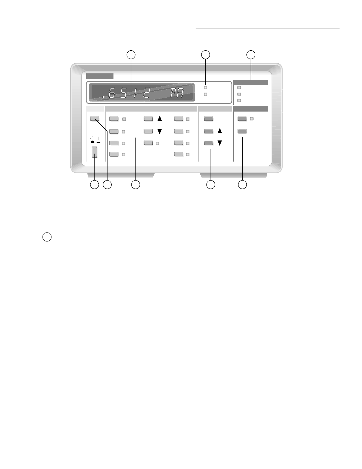
Operation
KEITHLEY
SHIFT
POWER
12 3
Figure 2-1
Model 6512 front panel
6
6512 PROGRAMMABLE ELECTROMETER
ELECTROMETER PROGRAM DATA STORE
VOLTS
OHMS
COUL
AMPS
RANGE
AUTO
MAX INPUT
250V
ZERO CHECK
ZERO CORRECT
SUPPRESS
TRIG SGL
7
METER
DATA
SELECT EXIT
ADJUST
4
8
STATUS
TALK
LISTEN
REMOTE
ON/OFF
RECALL EXIT
5
3 ELECTROMETER
The ELECTROMETER buttons control the measuring functions, selection of instrument ranges, and such items as zero
check, zero and suppression, and front panel triggering.
VOLTS—The VOLTS button places the instrument in
the DC volts measuring mode. When VOLTS is pressed,
the indicator next to the button turns on, showing that the
instrument is set for that mode. Note that the Model 6512
will be in this mode when it is first turned on. Pressing
SHIFT/VOLTS will place the instrument in the external
feedback mode, as described in paragraph 2.9.
OHMS—Pressing OHMS places the unit in the resistance measuring function. The indicator next to the
OHMS button will be illuminated when the instrument is
in this mode. Note that the instrument measures resistance using the constant-current method.
COUL—The Model 6512 may be set up to measure
charge by pressing the COUL button. The indicator next
to the COUL button will illuminate when the instrument
is set for this mode.
AMPS—Pressing AMPS switches the instrument to the
current-measuring function. The AMPS indicator will
turn on when the instrument is in this mode.
RANGE—These two buttons allow you to increment or
decrement the range the instrument uses. Pressing the ▲
button will move the instrument up one range each time
it is operated, while the ▼ button will move the instrument down range one increment each time it is pressed.
Note that pressing either of these buttons will cancel
auto-range if that mode was previously selected. The display mantissa will remain blank until the first reading is
ready to be displayed.
AUTO—The AUTO button places the instrument in the
auto-range mode. While in this mode, the Model 6512
will switch to the best range to measure the applied signal. Note that the instrument will be in the auto-range
mode when it is first turned on. Auto-ranging is a v ailable
for all functions and ranges. Auto-ranging may be cancelled either by pressing the AUTO button or one of the
two RANGE buttons.
2-3
Page 23

Operation
ZERO CHECK—The zero check mode is used in conjunction with the ZERO CORRECT control to cancel
any offsets within the instrument and is also used as a
standby mode. Pressing ZERO CHECK once will enable
this mode, as shown by the associated indicator light.
When zero check is enabled, the electrometer input circuit configuration changes (see paragraph 2.10). No
readings can be taken with zero check enabled. Pressing
ZERO CHECK a second time will disable this mode.
Zero check should be enabled when making connections
(except for coulombs) or when changing functions.
ZERO CORRECT—The zero correct mode works with
zero check to cancel electrometer offsets. If zero check is
enabled, pressing ZERO CORRECT will store a new of fset value that will be used to cancel any offset. If the
range is changed while zero correct is enabled, the stored
value will be scaled accordingly. Zero correct may be
cancelled by pressing the ZERO CORRECT button a
second time. More information on using zero correct
may be found in paragraph 2.10.
SUPPRESS—The suppress mode allows you to cancel
external offsets or to store a baseline value to be subtracted from subsequent readings. For example, if you applied 10V to the instrument and enabled suppress, that
value would then be subtracted from subsequent readings. Once suppress is enabled, the value is scaled when
the range is changed. Suppress may be disabled by pressing the SUPPRESS button a second time and is cancelled
if the function is changed.
TRIG—The TRIG button allows you to enter the oneshot trigger mode and trigger single readings from the
front panel. To enter the one-shot mode, press SHIFT
then TRIG. The SGL indicator light will show that the instrument is in the one-shot mode. Each time the TRIG
button is pressed, a single reading will be processed and
displayed. The displayed reading will flash when the
TRIG button is pressed. The one-shot trigger mode can
be cancelled by pressing SHIFT then TRIG a second
time. Additional information on triggering may be found
in paragraphs 2.12 and 3.2.12 in Sections 2 and 3.
4 PROGRAM
These keys allow access to Model 6512 front panel programs, which control the IEEE-488 primary address, set alpha or numeric exponent, and perform instrument calibration. Front panel programs are described in paragraph 2.5.
SELECT/EXIT—This button enters the program mode
to allow access to parameters described above. Pressing
SELECT repeatedly causes the instrument to scroll
through a program menu. To cancel the program mode,
press SHIFT and then SELECT/EXIT in that order. Note
that the program mode is also cancelled by pressing SELECT/EXIT after a program parameter change is made.
ADJUST—These two buttons set program parameters,
as described in paragraph 2.5.
5 DATA STORE
The two DATA STORE buttons control the internal 100reading data store mode of the instrument. Through these
two buttons, data storage may be enabled or disabled, the
storage rate may be selected, and readings may be recalled to
the front panel display. Paragraph 2.11 contains a complete
description of data store operation.
ON/OFF—This control enables or disables data store operation. In addition, reading rates can be selected by
holding the button in when first enabling data store.
When data store is enabled, the indicator light next to the
ON/OFF button will be on. Minimum and maximum values are stored and up-dated as long as the ON/OFF LED
is on.
RECALL/EXIT—This single button serves to recall
readings previously stored by data store. Pressing and
holding this button causes the instrument to scroll
through data store locations as indicated on the display.
Once the desired reading number is displayed, releasing
the button causes the actual reading to be displayed. To
exit the recall mode, press SHIFT then EXIT.
2-4
Page 24

Operation
2.4.2 Display and indicators
The operation of the 4 ½ digit display and various indicators
is described below. The display updates at about three readings per second in the continuous trigger mode.
6 Display
The Model 6512 has a display made up of a 4 ½ digit signed
mantissa as well as a two-digit signed exponent. The exponent can be represented either in scientific notation, or with
an alphanumeric subscript such as nA. The exponent display
mode can be changed with a front panel program, as described in paragraph 2.5. When scientific notation is used,
the decimal point remains fixed as in 1.9999, and the range
is indicated by the exponent. In addition, the display has a
number of front panel error messages that may occur during
operation; see Table 2-2.
Table 2-2
Display error messages
Message Description
OL Over-range input applied (- for nega-
tive value).
b Err Bus Error: Instrument programmed
while not in remote, or illegal command or option sent.
n Err Number Error: Calibration value out of
limits.
t Err Trigger Error: Instrument triggered
while processing reading from previous trigger.
8 STATUS indicators
These three indicators apply to operation of the Model 6512
over the IEEE-488 bus. The REMOTE indicator sho ws when
the instrument is in the IEEE-488 remote state, while the
TALK and LISTEN indicators show when the instrument is
in the talk and listen states respectively. See Section 3 for
more information on using the Model 6512 over the IEEE488 bus.
2.4.3 Tilt bail
The tilt bail, which is located on the bottom of the instrument, allows the front panel to be elevated to a convenient
viewing height. To extend the bail, rotate it out 90° from the
bottom cover and latch it into place. To retract the bail, pull
out until it unlatches, and rotate it against the bottom cover.
2.5 Front panel programs
The Model 6512 has three front panel programs that can be
used to set the primary address, set the display exponent
mode (alpha or numeric), or calibrate the instrument from
the front panel. To select a program, press PROGRAM SELECT button repeatedly while observing the display . The instrument will scroll through the available programs with
identifying messages, as shown in Table 2-3. When in the
program mode, the DATA STORE RECALL button is inoperative; the data store mode may be turned off, but not on.
The operation of the various programs is described in the following paragraphs. To exit a program, press SHIFT EXIT. If
a change was made, pressing SELECT alone will exit the
program.
7 METER and DATA indicators
The METER indicator identifies when the display is showing
a normal reading. The DATA LED indicates when the instrument is displaying DATA STORE information; a data store
reading is displayed when the DAT A LED is turned on. Usually, the display will sho w normal readings (METER on), but
the RECALL button will switch the display to the data store
mode.
Table 2-3
Front panel program messages
Message Program description
IEEE Displays/sets IEEE-488 primary
address.
dISP Sets numeric or alpha exponent.
CAL* Allows instrument calibration.
* Not normally accessible unless enabled. See paragraph 7.4.9.
2-5
Page 25

Operation
2.5.1 IEEE-488 address
Selection of the IEEE-488 address program is indicated by
the following message:
IEEE 27
Along with the message, the presently programmed IEEE488 address (the factory default value of 27 in this example)
will be displayed. To select a new address, use the ADJUST
keys. When the desired value is shown in the display, press
SHIFT then SELECT EXIT to return to normal operation (or
if a change was made, simply press SELECT). For complete
information on using the Model 6512 over the IEEE-488 bus,
refer to Section 3.
2.5.2 Exponent mode (alpha or numeric)
The display exponent of the Model 6512 can be operated in
either the alpha mode or the numeric mode. In the alpha
mode, the exponent is given in actual units such as mA. In
the numeric mode, the exponent is given in scientific notation. Table 2-4 gives typical examples, including units.
The display in the alpha mode appears as:
dISPm
Once the desired exponent mode is selected, press SHIFT
then SELECT EXIT to return to normal operation (or simply
PROGRAM SELECT if a change was made).
Table 2-4
Typical display exponent values
Engineering
Display
units
PA pA 10
nC nC 10
µA µA 10
mV mV 10
k Ω
M Ω
G Ω
k Ω
M Ω
G Ω
Scientific
notation Value
-12
A Picoamperes
-9
C Nanocoulombs
-6
A Microamperes
-3
V Millivolts
3
10
10
10
Ω
6
Ω
9
Ω
Kilo-ohms
Mega-ohms
Giga-ohms
To select the exponent program, scroll through the program
menu until the following message is displayed:
dISP
Use either of the ADJUST buttons to set the exponent to the
desired mode. In the numeric mode, the display might show:
dISP -3
2.5.3 Calibration
An advanced feature of the Model 6512 is its digital calibration program. The instrument can be calibrated from the
front panel or over the IEEE-488 bus. To use the front panel
calibration program, refer to the calibration procedures outlined in Section 7, paragraph 7.4.9.
2.6 Rear panel familiarization
The rear panel of the Model 6512 is shown in Figure 2-2.
2-6
Page 26

PEAK
500V
OFF
OFF
V, Ω GUARD
LO
250V PEAK
V, Ω GUARD
INPUT
INPUT
TRIAX
PREAMP
ON
GUARD
(FOLLOWS
INPUT)
DO NOT FLOAT INPUT LO
WITH PREAMP OUT COM
CONNECTED TO EARTH.
!
ON
10K
!
100
CAUTION:
ADDRESS ENTERED WITH
FRONT PANEL PROGRAM
6
PREAMP OUT
2V ANALOG OUTPUT
COM
!
IEEE 488 INTERFACE
SH1
AH1T5TE0L4LE0
SR1
RL0
PP0
PREAMP OUT
!
ANALOG OUTPUT
DC1C0E1
7
COM
2V
SLOWBLOW
1/8A 90-125V
1/16A 180-250V
LINE
FUSE
9
8
COMPLETE
10 11
IEEE COMMON
LINE VOLTAGE
SELECTED
(INTERNAL)
105-125V
210-250V
LINE RATING
50-60 HZ
15VA MAX
EXTERNAL
TRIGGER
INPUT
METER
OUTPUT
Operation
1
23
Figure 2-2
Model 6512 rear panel
1 INPUT
The INPUT connector is a 3-lug female triax connector to be
used for all electrometer signal inputs. Note that you should
not confuse a triaxial connector with the BNC type that is
used for the EXTERNAL TRIGGER and ELECTROMETER COMPLETE connections. Also, do not attempt to force
2-lug triaxial connector onto the INPUT connector. (See
paragraph 1.9 for details on 2-lug to 3-slot triax adapters.)
CAUTION
Do not float INPUT LO with preamp
out COM connected to earth (chassis
ground).
2 V, Ω GUARD Switch
4
5
3 IEEE-488 Connector
This connector is used to connect the instrument to the IEEE488 bus. IEEE-488 function codes are marked above the connector.
4 LINE FUSE
The LINE FUSE, which is accessible on the rear panel, provides protection for the AC power line output. For information on replacing this fuse, refer to Section 7.
5 AC Receptacle
Power is applied through the supplied power cord to the AC
receptacle. Note that the supply voltage is marked adjacent
to the receptacle.
The V, Ω GUARD switch adds capabilities for connecting a
guard voltage to the inner shield of the input cable. Guarding
is useful in the volts and ohms modes to speed up response
time and minimize the effects of leakage resistance and stray
capacitance. Note that guarded operation is not recommended in amps or coulombs modes. See paragraph 2.7.4 for more
information on guarded operation.
6 Chassis Ground
This jack is a 5-way binding post that is connected to instrument chassis ground. It is intended for use in situations requiring an accessible chassis ground terminal. A shorting
link is supplied and connected between the chassis ground
and COM terminals.
2-7
Page 27

Operation
7 PREAMP OUT
The PREAMP OUT jack provides a guard output for voltage
and resistance measurements. This output can also be used as
an inverting output or with external feedback when measuring current or charge. The PREAMP OUT has a maximum
output value of ±300V and uses a standard 5-way binding
post.
WARNING
Hazardous voltage may be present at
the PREAMP OUT, depending on the
input signal.
8 COM Terminal
The COM terminal is a 5-way binding post that provides a
low connection for both the 2V AN ALOG OUTPUT and the
PREAMP OUT . This terminal is also used for input lo w connection when in guarded mode; COM is internally connected
to input low through a 100 Ω
resistor.
CAUTION
2.7 Basic measurement techniques
The paragraphs below describe the basic procedures for using the Model 6512 to make voltage, resistance, charge, and
current measurements.
2.7.1 Warm-up period
The Model 6512 is usable immediately when it is first turned
on. However, the instrument must be allowed to warm up for
at least two hours to achieve rated accuracy.
NOTE
While rated accuracy is achieved after the
two-hour warm up period, input bias current may require additional time to be reduced to its optimum level. Allow two
more hours for input bias current to settle
to less than 10fA and eight hours for settling to less than 5fA. In sensitive applications, it is preferable for the unit to be left
on continuously.
Do not connect PREAMP OUT, COM,
or 2V ANALOG OUTPUT to earth
ground when floating the input.
9 2V ANALOG OUTPUT
The 2V ANALOG OUTPUT provides a scaled 0-2V output
from the electrometer (2V output for full range input). The
output uses a standard 5-way binding post and is inverting in
the volts and ohms modes.
10 METER COMPLETE OUTPUT
This BNC connector provides an output pulse when the
Model 6512 has completed a reading; it is useful for triggering other instrumentation.
11 EXTERNAL TRIGGER INPUT
This BNC connector can be used to apply external trigger
pulses to the Model 6512 to trigger the instrument to take one
or more readings, depending on the selected trigger mode.
2.7.2 Input connections
The rear panel INPUT connector is a Teflon-insulated, 3-lug
female triax connector intended for all input signals to the
Model 6512. As shown in Figure 2-3, the center terminal is
high, the inner ring or shield is low, and the outer shield is
connected to instrument chassis ground. In the guarded
mode, the inner shield is driven at guard potential, while the
outer shield is chassis ground.
NOTE
The INPUT connector must be kept clean to
maintain high input impedance. Place the
supplied rubber dust cap on the INPUT connector when the instrument is not in use.
2-8
Page 28

INPUT HI
INPUT HI
60Hz sine wave (10 seconds maximum
in mA ranges). Exceeding this value
may cause damage to the instrument.
Operation
INPUT LO
CHASSIS
GROUND
A. UNGUARDED
(V, Ω GUARD OFF)
GUARD
CHASSIS
GROUND
100Ω
COM
B. GUARDED
(V, Ω GUARD ON)
Figure 2-3
Input connector configuration
The supplied Model 237-ALG-2 cable is designed to mate with
the INPUT connector. The other end of the Model 237-ALG-2
is terminated with three alligator clips. Input high is color coded
in red, input low is colored black, and chassis ground is color
coded in green. Keep in mind that these connections are for the
unguarded mode. In the guarded mode, red is high, black is
guard, and green is chassis ground. The COM binding post provides a connection to input low through 100 Ω for use in the
guarded mode.
NOTE
It is recommended that zero check be enabled when connecting or disconnecting
input signals.
2.7.3 Making voltage measurements
The Model 6512 can be used to measure voltages in the
range of ±10µV to ±200V. In principle, the instrument operates much like an ordinary DMM, but its special characteristics allow it to make measurements in cases where an
ordinary DMM would be unable to perform well. In particular, the very high input resistance of 200T Ω (2 × 10
lows it to accurately measure voltage sources with high
internal resistances. In contrast, an ordinary DMM may have
an input resistance of only 10M Ω , resulting in inaccurate
measurements because of instrument loading.
Use the following procedure to make voltage measurements:
1. Turn on instrument po wer, and allo w the unit to warm up
for two hours to reach rated accuracy.
2. Check to see that the voltage function is selected by
pressing the VOLTS button. Use the auto-range mode,
or select the desired range with the ranging pushbuttons.
3. To achieve specified accuracy, especially on the lower
ranges, it is recommended that you zero the instrument.
To do so, first enable zero check, and then press the
ZERO CORRECT button. Correcting zero on the lo west
range of any function will correct all ranges because of
internal scaling.
14
Ω ) al-
WARNING
The maximum common-mode input voltage (the voltage between input low and
chassis ground) is 500V peak. Exceeding
this value may create a shock hazard.
CAUTION
Connecting PREAMP OUT, COM, or 2V
ANALOG OUTPUT to earth while floating the input may damage the instrument.
CAUTION
The maximum voltage between input
high and input low is 250V RMS, DC to
NOTE
The input circuit configuration changes
with zero check enabled. See paragraph
2.10.1 for details.
4. Connect the supplied Model 237-ALG-2 triaxial input
cable or other suitable triax cable to the rear panel INPUT jack. For sources with high output resistance, the
cable should be kept as short as possible to minimize cable capacitance.
5. If response time and leakage resistance are considerations, place the instrument in the guarded mode as described in paragraph 2.7.4.
6. Connect the other end of the cable to the voltage to be
measured, as shown in Figure 2-4. Disable zero check.
2-9
Page 29

Operation
A
B
7. Take the reading directly from the display. The exponent can be placed either in the alpha or numeric mode, as described
in paragraph 2.5.
Voltage measurement considerations
Two factors are of concern when making voltage measurements, especially for voltage sources with high output (source) resistances. For one thing, the loading effects of the measuring instrument come into play at the high resistance lev els in v olved. Secondly, the distributed capacitance of the source, the input cable, and the input circuit of the instrument itself are a factor when
making these measurements.
Figure 2-5 demonstrates how meter loading can affect measurement accuracy. Here, a voltage source with a value E
source resistance R
is connected to the input of the electrometer. The input resistance of the electrometer is R
S
. The percent
IN
error due to loading can be calculated as follows:
100R
S
ERROR
%
------------------------=
RSR
+
IN
Thus, to keep the error under 0.1%, the input resistance must be about 1000 times the value of the source resistance, R
that the Model 6512 input resistance is ≥ 200G Ω , but the cable resistance appears in parallel.
Figure 2-5
Meter loading considerations
INPUT
TRIAX CABLE
SOURCE
E
R
S
S
R
IN
METER
V
and a
S
. Note
S
ON
OFF
V, Ω GUARD
MODEL 6512
V
S
GND
Figure 2-4
Connections for voltage measurements
2-10
HI
LO
INPUT AMPLIFIER
PREAMP OUT
COM
At very high resistance levels, the very large time constants
created by even a minimal amount of capacitance can slow
down response time considerably. For example, measuring a
source with an internal resistance of 100GΩ would result in
an RC time constant of one second when measured through
a cable with a nominal capacitance of 10pF. If 1% accuracy
is required, a single measurement would require at least five
seconds. Note that typical input cables have unguarded capacitance (high to inner shield) of 120 to 150pF per meter.
Basically, there are two ways to minimize this problem: (1)
keep the input cable as short as possible, and (2) use guarding.
With the first method, there is a limit as to how short the cable
can be. Using guarding can reduce these effects and decrease
settling times by up to a factor of 1,000. The Model 6512 rear
Page 30

Operation
O
6512
PREAMP
Z
L
R
S
E
S
A=1
OV
Z
S
(
SHIELD)
E
O
panel V, Ω GUARD switch allows guarding to be easily applied to the input circuit; see paragraph 2.7.4 for details.
At low signal levels, noise may affect accuracy. Shielding of
the unknown voltage can reduce noise effects substantially.
When using shielding, the shield should normally be connected to input low , although connecting the shield to chassis
ground may yield better results in some cases.
2.7.4 Guarded operation
Guarding consists of using a conductor driven by a low-impedance source to totally surround the leads carrying a highimpedance signal. The output of this low-impedance source
is kept at the same potential as the signal itself, resulting in
drastically reduced leakage currents.
To approach the concept of guarding, let us first review the
unguarded circuit shown in Figure 2-6. The measured signal
is represented by the voltage source ES and the source resistance RS. Cable leakage impedance is represented by ZL.
The source resistance and leakage impedance form a voltage
divider that attenuates the source voltage as follows:
ZLE
S
---------------------=
E
O
ZLR
+
S
ES ZL
EO =
RS + ZL
R
Z
L
R
S
E
S
A. BASIC CONFIGURATION
E
O
S
E
S
B. EQUIVALENT CIRCUIT
Z
L
ty-gain amplifier with a high input impedance and low output
impedance is used. The input of the amplifier is connected to
the signal, while the output is used to drive the shield. Since
the amplifier has unity gain, the potential across ZL is typically <1mV, so no leakage current flows. Leakage between
the cable shield and ground may be considerable, but it is of
no consequence since that current is supplied by the low-impedance source, rather than by the signal itself.
Figure 2-7
Guarded circuit
When the rear panel V, Ω/ GUARD switch is placed in the
ON position, guard potential is placed on the inner shield of
the triaxial cable. The outer shield remains at chassis ground.
Thus, it is necessary to use the COM terminal for low signal
connections, as shown in Figure 2-8. For very critical measurements, a shielded, guarded enclosure should be used.
WARNING
Hazardous voltage (up to 300V) may be
present on the inner shield when V, Ω/
E
GUARD is on, depending on the input
signal. A safety shield, connected to chassis ground is recommended when making voltage measurements over 30V or
for guarded resistance measurements.
Figure 2-6
Unguarded circuit
The use of guarding is not recommended
NOTE
for the amps or coulombs functions.
Thus, to keep the error due to leakage resistance under 0.1%,
the leakage resistance must be at least 1,000 times the source
resistance value.
Guarding the circuit minimizes these effects by driving the
shield at signal potential, as shown in Figure 2-7. Here, a uni-
The PREAMP OUT terminal may be used for guarding in
the volts and ohms modes in a similar manner. In this mode,
2-11
Page 31

Operation
TRIAX CABLE
OFF
V, Ω GUARD
HI
LO
SAFETY SHIELD
Figure 2-8
Guarded input connections
INPUT
ON
MODEL 6512
HI
GUARD
GND
COM
PREAMP OUT
LO
COM
A. CONNECTIONS
V, Ω
GUARD
SWITCH
INPUT AMPLIFIER
100Ω
S
B. EQUIVALENT CIRCUIT (VOLTS MODE SHOWN)
HI
GUARD
GND
LO
WARNING: USE SAFETY SHIELD FOR SIGNALS
RANGING AMPLIFIER
S
HI
MEASURED
DEVICE
LO
GUARD
SAFETY SHIELD
ABOVE 30V (VOLTS) AND OHMS
TO A/D
CONVERTER
2V ANALOG
OUTPUT
the preamplifier acts as a unity-gain amplifier with low output impedance.
WARNING
Hazardous voltage (up to 300V) may be
present at the PREAMP OUT terminal,
depending on the input signal.
2.7.5 Making current measurements
The Model 6512 can resolve currents as low as 0.1fA
-16
(10
A), and measure as high as 20mA in 11 ranges. The
Model 6512 exhibits low input voltage b urden and extremely
low input offset current. The low voltage burden is achieved
because the Model 6512 measures current as a feedback type
picoammeter, rather than the shunt method used by many
DMMs.
CAUTION
Safe operation and good measurement
practice dictates the use of an external
resistor when necessary to limit currents
to less than 30mA.
NOTE
After measuring high voltage in volts, or
following an overload condition in ohms,
it may take a number of minutes for input
current to drop to within specified limits.
Input current can be verified by placing a
shielded cap on the INPUT jack and then
connecting a jumper between the COM
and chassis ground terminals. W ith the instrument on the 2pA range and zero check
disabled, allow the reading to settle until
the instrument is within specifications.
2-12
Page 32

Operation
To measure current with the Model 6512, use the following
procedure:
1. Turn on the po wer , and allo w the instrument to warm up
for at least two hours to obtain rated accuracy.
2. Select the current mode by pressing the AMPS b utton on
the front panel. Set the V, Ω/ GUARD switch to OFF.
3. T o achiev e rated accuracy , select the 2pA range, zero the
instrument by enabling zero check and then pressing the
ZERO CORRECT button. After zero correction, select
the desired range, or use auto-ranging if desired.
TRIAX CABLE
INPUT
OFF
ON
VΩ, GUARD
MODEL 6512
INPUT
AMPLIFIER
Z
INPUT
HI
I
S
LO
S
GND
F
PREAMP
OUT
COM
4. Connect a suitable triax cable to the rear panel INPUT
jack. Connect the other end of the circuit to be measured
as shown in Figure 2-9. Shielding will be required for
low-level measurements. Connect the shield to input
low.
5. Disable zero check, and allow the reading to settle.
6. Read the current value directly from the display . The e xponent may be placed either in the alpha or numeric
modes, as described in paragraph 2.5.
HI
I
S
MEASURED
CURRENT
SHIELD
BELOW 1µA
TO A/D
CONVERTER
2V ANALOG
OUTPUT
A. CONNECTIONS
RANGING
AMPLIFIER
B. EQUIVALENT CIRCUIT
LO
100Ω
RECOMMENDED
S
Figure 2-9
Current measurements
2-13
Page 33

Operation
Current measurement considerations
At very low lev els (in the picoampere range or below), noise
currents generated in the cable or from other sources can affect measurements. Currents generated by triboelectric effects are a primary cause of noise currents generated in
connecting cables. These currents are generated by charges
created at the junction between a conductor and an insulator
because of friction. Coaxial and triaxial cables are especially
prone to such noise currents, which are generated by cable
flexing. To minimize these effects, the cable should be tied
down firmly to minimize any flexing. Also, special lo w-noise
cable, constructed with graphite between the shield and insulator, is available to minimize these effects (see paragraph
1.9). However, even with low-noise cables, several tens of
femtoamps of noise currents can be generated by cable
movement.
SOURCE
R
E
S
I
S
METER
E
IN
(VOLTAGE
BURDEN)
Figure 2-10
Voltage burden considerations
2.7.6 Making charge measurements
I =
ES - E
IN
R
S
Voltage burden is frequently a consideration when making
current measurements. Ideally, the input voltage burden
should be zero for the instrument to have absolutely no effect
on the circuit it is measuring. If the voltage burden is too high,
its effects can degrade measurement accuracy considerably.
T o see ho w voltage b urden can upset measurement accurac y,
refer to Figure 2-10. A source, represented by E
with an out-
S
put resistance RS, is shown connected to the input of a picoammeter. The voltage burden is represented by a constant
voltage source at the input as EIN. If EIN were zero, the current as seen by the meter would simply be:
E
S
I
-------=
R
S
However, if EIN has a non-zero value, the current now becomes:
ESE
–
I
IN
-----------------------=
R
S
Note that the Model 6512 voltage burden is typically 1mV or
less. Additional considerations include source resistance and
capacitance, as discussed in paragraph 2.13.
The Model 6512 is equipped with three coulombs ranges to
resolve charges as low as 10fC (10
-14
C) and measure as high
as 20nC (20 × 10-9C). When the instrument is placed in one
of the coulombs ranges, an accurately known capacitor is
placed in the feedback loop of the amplifier so that the voltage developed is proportional to the integral of the input cur rent in accordance with the formula:
i dt
Q
S
------- -==
C
1
----
V
idsst
∫
∫
C
The voltage is scaled and displayed as charge.
NOTE
After measuring high voltages in volts, or
following an overload condition in ohms,
it may take a number of minutes for the input current to drop to within specified limits. Input current can be verified by placing
a shielded cap on the INPUT jack and then
connecting a jumper between the COM
and chassis ground terminals. W ith the instrument on the 2pA range and zero check
disabled, allow the reading to settle until
the instrument is within specifications.
2-14
Page 34

Operation
Normal charge measurements
Use the following procedure to measure charge with the
Model 6512:
1. Turn on the power, and allow a two-hour warm up period for rated accuracy.
2. Place the instrument in the coulombs mode by pressing
the COUL button. Set V, Ω/ GUARD to OFF.
3. To achieve rated accuracy, place the instrument on the
200pC range, and zero the instrument by enabling zero
check and then pressing the ZERO CORRECT button.
4. Select the desired range, or use auto-ranging, if desired.
5. Disable zero check. A small amount of zero check hop
(sudden change in the reading) may be observed when
TRIAX CABLE
INPUT
zero check is disabled. If desired, enable suppress to null
out any zero check hop, which typically will be in the
10-25 count range.
6. Connect the triax cable to the INPUT jack. Connect the
other end of the cable to the circuit being measured, as
shown in Figure 2-11. For low-level measurements,
shielding may be required.
NOTE
Do not connect the circuit to the instrument with zero check enabled.
7. Read the charge value from the display. The exponent
may be placed either in the alpha or numeric modes as
described in paragraph 2.5.
NOTE: LEAVE QS DISCONNECTED
UNTIL ZERO CHECK DISABLED
HI
Q
S
MEASURED
CHARGE
LO
Q
Figure 2-11
Coulombs connections
ON
OFF
V, Ω GUARD
S
MODEL 6512
HI
LO
GND
INPUT AMPLIFIER
C
F
1000pF
S
PREAMP
OUT
COM
A. CONNECTIONS
B. EQUIVALENT CIRCUIT
S
100Ω
SHIELD (OPTIONAL)
S
TO A/D
CONVERTER
2V ANALOG
OUTPUT
2-15
Page 35

Operation
Using the coulombs function to measure current
Note that the coulombs function can also be used to measure
current. The advantage of doing so is that noise in the measurement is substantially reduced because of the integrating
process. To measure current using the coulombs function,
proceed as follows:
1. Place the instrument in the coulombs function, and select the desired range, or use auto-ranging, if desired.
2. Enable zero check, and connect the current to be measured to the INPUT jack (see Figure 2-9).
3. Disable zero check, and note the charge measurement at
the end of a specific interval of time (for example, 10
seconds).
4. To determine the current, simply divide the measured
charge by the time in seconds. For example, if a charge
of 12nC is seen after a 10-second interval, the current is
12nC/10 = 1.2nA. (Using Data Store at a 10-second rate
can simplify the process.)
5. As an alternative to the abov e procedure, connect a chart
recorder to the 2V AN ALOG OUTPUT (paragraph 2.9),
and graph the measured charge. Since the current is given by I=dQ/dt, the current at any point is equal to the
slope of the graph at that point, after applying the appropriate scaling factor (100pC/V, 200pC range; 1nC/V,
2nC range; 10nC/V, 20nC range).
CAUTION
Connecting PREAMP OUT, COM, or
2V ANALOG OUTPUT to earth while
floating input may damage the instrument.
Charge measurement considerations
A primary consideration when making change measurements is the input offset current of the integrating amplifier.
Any such current is integrated along with the input signal
and reflected in the final reading. The Model 6512 has a max-
imum input offset current of 5 × 10
-15
A at 23°C. This value
doubles every 10°C. This input offset current translates into
a charge of 5 × 10
-15
C per second at a temperature of 23°C.
This value must be subtracted from the final reading to obtain the correct value.
When using an external voltage source, the input current
should be limited to less than 1mA by placing a resistor in series with the high input lead. The value of this resistor should
be at least: R=1000 × VS (in ohms) where V is the voltage
source value, or the compliance of the current being integrated.
2.7.7 Resistance measurements
The Model 6512 makes resistance measurements using the
constant-current method. (A current is forced through the
DUT, and the voltage across the DUT is measured.). The instrument can resolve resistances as low as 0.1Ω and measure
as high as 200GΩ.
To measure resistance with the Model 6512, use the following procedure:
1. Turn on the po wer, and allow a two-hour warm-up period for rated accuracy.
2. Press the OHMS button to select the ohms mode.
3. For maximum accuracy, place the instrument on the
2kΩ range, and zero the instrument by enabling zero
check and then pressing the ZERO CORRECT button.
4. Select the desired range, or use auto-ranging, if desired.
5. Connect the triax cable to the INPUT jack. Keep the cable
as short as possible to minimize the effects of cable capacitance. Connect the other end of the cable to the resistance to be measured, as shown in Figure 2-12. For
measurements above 1GΩ, it is recommended that you
use guarded connections, as described in paragraph 2.7.4.
6. Disable zero check, and allow the reading to settle.
7. T ake the reading from the display. The exponent may be
placed in either the alpha or numeric modes, as described in paragraph 2.5.
2-16
Page 36

TRIAX CABLE
Operation
INPUT
ON
OFF
V, Ω GUARD
R
X
MODEL 6512
INPUT
I
RX
HI
LO
GND
AMPLIFIER
S
INPUT
R
PREAMP
OUT
COM
A. CONNECTIONS
F
V
R
B. EQUIVALENT CIRCUIT
HI
LO
(RECOMMENDED ABOVE 100MΩ)
RANGING AMPLIFIER
S
100Ω
S
R
X
MEASURED
RESISTANCE
SHIELD
CONVERTER
TO A/D
2V ANALOG
OUTPUT
Figure 2-12
Resistance measurement connections
Resistance measurement considerations
When measuring high resistance values, there are two primary factors that can affect measurement accuracy and speed.
Any leakage resistance in the connecting cable or test fixture
can decrease the actual resistance seen by the instrument. Also, capacitance of the cable or input circuit can slow down
the response time considerably.
These two problems can be minimized by using guarding,
especially when measuring resistances above 1GΩ. Guarding is further discussed in paragraph 2.7.4. Noise pickup can
also be a problem, in which case the resistor must be shielded. Connect the shield to input low.
At low resistances, lead resistance can be a consideration.
Cancel the effects of lead resistance by shorting the ends of
the input leads and enabling suppress with zero check disabled. Leave suppress enabled for subsequent measurements.
2.7.8 Using the ohms function as a current source
The Model 6512 ohms function may also be used to generate
currents in decade values between 1nA and 100µA. To use
the instrument in this manner, simply connect the triax cable
to the INPUT jack, and connect the other end of the cable to
the circuit under test. Select the resistance range in accordance with the desired current (see Table 2-5). Note that current flows out from input high into input low . The test voltage
is less than 2V for all ranges 2GΩ and less, except when an
overload occurs, in which case the compliance voltage is
300V.
2-17
Page 37

Operation
Table 2-5
Ohms function current output values
Ranges Output current (±1.5%)
2kΩ, 20kΩ 100µA
200kΩ 10µA
2MΩ 1µA
20MΩ 100nA
200MΩ 10nA
2GΩ, 20GΩ, 200GΩ 1nA
2.8 Analog outputs
The Model 6512 has two analog outputs on the rear panel.
The 2V ANALOG OUTPUT provides a scaled 0-2V output
with a value of 2V corresponding to full-range input. The
PREAMP OUT is especially useful in situations requiring
buffering. These tw o analog outputs are discussed in the following paragraphs.
WARNING
When floating Input Low above 30V
RMS from earth ground, hazardous
voltage will be present at the analog outputs. Hazardous voltage may also be
present when measuring in ohms, or
when the input voltage exceeds 30V
RMS in the volts mode.
2.8.1 2V analog output
The 2V ANALOG OUTPUT provides a scaled 0-2V output
that is inverting in the volts and ohms modes. Connections
for using this output are shown in Figure 2-13. For a fullrange input, the output will be 2V ; typical examples are listed
in Table 2-6. The 2V ANALOG OUTPUT signal is not corrected during calibration. Gain errors of up to 3% may appear at this output, depending on function and range
selection.
Note that the output impedance is 10kΩ; to minimize the effects of loading, the input impedance of the device connected
to the 2V AN ALOG OUTPUT should be as high as possible.
For example, with a device with an input impedance of
10MΩ, the error due to loading will be approximately 0.1%.
Table 2-6
Typical 2V analog output values
Applied
Range
20pA 10.4pA 1.04V
2µA 1.65µA 1.65V
200mV 140mV 1.4V
200V 35V 0.35V
200kΩ 175kΩ 1.75V
20GΩ 9.5GΩ 0.95V
200pC 125pC 1.25V
20nC 19nC 1.9V
*Output values within ±3% of nominal value.
signal
Nominal 2V analog
output value*
2-18
CAUTION
Connecting PREAMP OUT, COM, or
2V ANALOG OUTPUT to earth while
floating the input may damage the instrument.
Page 38

Operation
LO
INPUT
OFF ON
V, Ω GUARD
MODEL 6512
COM
2V ANALOG OUT
RF =2MΩ (X10)
200kΩ (X1)
20kΩ (X0.1)
2kΩ (X0.01)
MODEL 1683
TEST LEAD KIT
A. CONNECTIONS
HI
MEASURING DEVICE
(EXAMPLE: CHART RECORDER)
INPUT FROM
PREAMP
200kΩ
S
MODEL 6512
Figure 2-13
Typical 2V analog output connections
2.8.2 Preamp out
The PREAMP OUT of the Model 6512 follows the signal amplitude applied to the INPUT terminal. Some possible uses for
PREAMP OUT include buffering of the input signal, as well as
for guarding in the volts and ohms modes. Connections and
equivalent circuits for the preamp output are sho wn in Figure 2-
14. Full-range outputs for various functions and ranges are listed in T able 2-7. Since the PREAMP OUT signal is not corrected during calibration, gain errors of up to 3% may appear at this
output, depending on function and range selection. For all volts
ranges, PREAMP OUTPUT accuracy is typically 5ppm.
WARNING
High voltage may be present between the
PREAMP OUT and COM terminals depending on the input signal (see Table 2-
10kΩ
100Ω
S
B. EQUIVALENT CIRCUIT
2V ANALOG OUTPUT
COM
INPUT RESISTANCE OF
RL =
MEASURING DEVICE
7). Open-circuit voltage of 300V is present
at PREAMP OUT in the ohms function.
CAUTION
Connecting PREAMP OUT, COM, or 2V
ANALOG OUTPUT to earth while floating input may damage the instrument.
Note that the PREAMP OUT output resistance is 100 Ω . The
output resistance appears between Input Low and Analog
Output Low to keep the resistor out of the loop when using
external feedback elements. To keep loading errors under
0.1%, the device connected to the PREAMP OUT should
have a minimum input impedance of 100k Ω
.
2-19
Page 39

Operation
PREAMP OUT
INPUT
OFF ON
V, Ω GUARD
MODEL 6512
HI
V
IN
LO
100Ω
S
GND
VOLTS
I
HI
R
X
LO
COM
V
OUT
PREAMP OUT
COM
S
V
OUT
PREAMP OUT
COM
= V
IN
R
= I R
A. CONNECTIONS
I
IN
L
X
Q
R
L
IN
MODEL 1683
TEST LEAD KIT
HI
LO
S
GND
HI
LO
S
HI
LO
MEASURING DEVICE
R
F
PREAMP OUT
AMPS
C
F
PREAMP OUT
100Ω
V
OUT
V
OUT
COM
= Q
COM
S
= -IINR
IN
C
F
F
R
L
R
L
S
GND
Figure 2-14
Typical preamp out connections
OHMS
100Ω
S
B. EQUIVALENT CIRCUITS
GND
100Ω
S
COULOMBS
2-20
Page 40

VIZ
FB
–=
Table 2-7
Full-range PREAMP OUT values
Full-range
Function Range
Volts 200mV
2V
20V
200V
Amps 2pA, 2nA, 2µA, 2mA
20pA, 20nA, 20µA, 20mA
200pA, 200nA, 200µA
Ohms* 2k Ω
20k Ω -2G Ω
20G
200G Ω
Coulombs 200pC
2nC
20nC
*W ARNING: Open-circuit voltage of 300V present at PREAMP OUT in ohms.
value
200mV
2V
20V
200V
200mV
2V
20V
200mV
2V
20V
200V
200mV
2V
20V
Operation
ohms). The maximum voltage span in external feedback
is
±20V.
2. The input impedance in the external feedback mode is
given by the relationship Z
IN
= Z
FB
/A
, where: Z
V
FB
is
the impedance of the external feedback network, and A
is the open-loop gain of the electrometer (typically
6
greater than 10
= 10M Ω || Z
). Note that the input impedance is Z
when zero check is enabled.
FB
IN
3. The voltage at the PREAMP OUT terminal is given by
the formula:
where Z
is the value of the feedback impedance.
FB
4. Any feedback elements should be housed in a suitable
shielded enclosure (see paragraph 2.9.2 below). Insulators connected to Input HI should be made of Teflon or
other high-quality insulating material and should be
thoroughly cleaned to maintain the high input impedance and low input current of the Model 6512. If these
insulators become contaminated, they can be cleaned
with methanol and then dried with clean, pressurized air.
C
FB
V
2.9 Using external feedback
The external feedback function provides a means to extend
the capabilities of the Model 6512 Electrometer to such uses
as logarithmic currents, non-decade current ranges, as well
as non-standard coulombs ranges. The following paragraphs
discuss the basic electrometer input circuitry and methods to
implement these functions.
2.9.1 Electrometer input circuitry
A simplified diagram of the electrometer input in the external
feedback mode is shown in Figure 2-15. An input current applied to the inverting (-) input of the op amp is nulled by a
current fed back through the internal feedback network made
up of R
pears at the PREAMP OUT, this internal network can be replaced by an external network connected between the
preamp output and Input HI connections. When using external feedback, the following factors must be taken into account:
and C
FB
. Because the output of the op amp ap-
FB
R
FB
ZERO CHECK
HIGH
INPUT
LOW
COM
PREAMP
OUT
OP AMP
100MΩ
S
100Ω
(CHASSIS)
TO RANGING
AMPLIFIER
Figure 2-15
Electrometer input circuitry (external feedback mode)
1. The maximum current value that can be supplied by the
preamp output is 20mA in amps (1mA in volts and
2-21
Page 41

Operation
2.9.2 Shielded fixture construction
Since shielding is so critical for proper operation of external
feedback, it is recommended that a shielded fixture similar to
the one shown in Figure 2-16 be used to house the feedback
element. The fixture is constructed of a commercially available shielded fixture modified with the standard BNC connectors replaced with triaxial female connectors. For
convenience, a banana jack can be mounted on the box to
make the necessary PREAMP OUT connection. Alternately,
a wire could be run through a rubber grommet mounted in a
hole in the side of the box. Note that input low is connected
to chassis ground within the shielded box. This connection
can be made by using a small solder lug secured with a
screw.
2.9.3 External feedback procedure
Use the following procedure to operate the Model 6512 in
the external feedback mode.
LO
SOLDER LUG
5
2
1. Connect the feedback element between the PREAMP
OUT terminal and the Input High terminal.
2. Place the instrument in the external feedback mode by
pressing the SHIFT then VOLTS buttons in that order.
The AMPS and V OLTS indicators will illuminate simultaneously in the external feedback mode.
3. The display will show the voltage measured at the output of the input preamplifier (PREAMP OUT). However, the “V” exponent will not appear as in the volts
mode. For example, with a 150mV output the display
will show:
150.00 m
(External feedback may be temporarily digitally calibrated as outlined in paragraph 7.4.16.)
4. The external feedback mode may be cancelled by pressing one of the four functions keys (VOLTS, OHMS,
COUL, or AMPS).
INPUT LOW (INNER SHIELD)
1
INPUT HIGH (CENTER CONDUCTOR)
2
4
TO 6512 INPUT JACK
TO PREAMP OUT
FEEDBACK
ELEMENT
HI
LO
GND
237-ALG-2
CABLE
ITEM DESCRIPTION MFR. PART NUMBER
1 SHIELDED FIXTURE POMONA #2390
2 FEMALE TRIAXIAL KEITHLEY 7078-TRX-TBC
3 BANANA JACK KEITHLEY BJ-9-2
4 TRIAXIAL CABLE KEITHLEY 237-ALG-2
5 TRIAXIAL CABLE KEITHLEY 7078-TRX-3
Figure 2-16
Shielded fixture construction
SHIELDED
FIXTURE
PARTS LIST
FROM SIGNAL
HI
FEEDBACK ELEMENT
3
A. CONSTRUCTION
PREAMP OUT
7078-TRX-3
CABLE
B. EQUIVALENT CIRCUIT
HI
LO
GND
S
6512 INPUT AMP
TO RANGING
AMP AND A/D
2-22
Page 42

Operation
2.9.4 Non-standard coulombs ranges
In its standard form, the Model 6512 has three coulombs
ranges allowing it to measure charge between 10fC and
20nC. Different charge measurement ranges can be used by
placing an external feedback capacitor between the
PREAMP OUT and Input HI and then placing the instrument
in the external feedback mode.
Charge is related to capacitance and voltage by the formula:
Q = CV, where Q is the charge in coulombs, C is the capacitance in farads, and V is the v oltage in volts. The Model 6512
display will read charge directly in units determined by the
value of C. For example, a 1µF capacitor will result in a displayed reading of 1µC/V.
In practice, the feedback capacitor should be greater than
100pF for feedback stability and of suitable dielectric material to ensure low leakage and low dielectric absorption.
Polystyrene, polypropylene, and Teflon dielectric capacitors
are examples of capacitor types with these desirable characteristics. The capacitor should be mounted in a shielded fixture like the one in Figure 2-16.
To discharge the external feedback capacitor, enable zero
check. The discharge time constant will be given by: τ =
(10M Ω ) (C
). Allow five time constants for discharge to
FB
within 1% of final value.
2.9.5 Logarithmic currents
The use of a diode junction in the external feedback path permits a logarithmic current-to-voltage conversion. This relationship for a junction diode is given by the equation:
V = mkT/q ln(I/I
where: q = unit of charge (1.6022 × 10
k = Boltzmann’s constant (1.3806 × 10
T = temperature (K).
The limitations in this equation center on the factors I
and R
. I
is the extrapolated current for V
B
O
proportional constant, m, accounts for the different character
current conduction (recombination and diffusion mechanisms) within the junction, typically varying between 1 and
2. Finally, R
constitutes the ohmic bulk resistance of the di-
B
) + IR
O
B
-19
)
. An empirical
O
-23
)
, m,
O
ode junction material. I
and R
O
limit the usefulness of the
B
junction diode at low and high currents respectively. The factor m introduces non-linearities between those two extremes.
Because of these limitations, most diodes have a limited
range of logarithmic behavior.
A solution to these constraints is to use a transistor configured as a “transdiode” in the feedback path, as shown in Figure 2-17. Analyzing the transistor in this configuration leads
to the relationship:
V = kT/q[ln(I/I
where h
is the current gain of the transistor.
FE
From this equation, proper selection of Q
device with high current gain (h
) - ln(h
O
/(1 + h
FE
), which is maintained
FE
))]
FE
would require a
1
over a wide range of emitter currents. Suitable devices for
this application include Analog Devices AD812 and Precision Monolithics MAT-01. Use the enclosure in Figure 2-16
to shield the device.
Frequency compensation/stabilization is accomplished by
adding a feedback capacitor, C
. The value of this capacitor
FB
depends on the particular transistor being used and the maximum current level expected. Compensation at maximum
current is required because the dynamic impedance will be
minimum at this point. It should be noted that the response
speed at lower currents will be compromised due to the increasing dynamic impedance, which is given by the following formula:
Z
dV
-------- kT==
dI
/qI = 0.026/I (@ 25°C)
Using the above transistors, a minimum RC time constant of
100µsec at maximum input current would be used. At I
IN
(max) of 100µA, this value would correspond to 0.4µF. Note
that at 100nA, this value would increase the RC response
time constant to 100msec. A minimum capacitance of 100pF
is recommended.
Although the input signal to this particular circuit is assumed
to be a current, conversion to voltage input could be performed by placing a shunt resistor across the input. However ,
the nominal voltage burden of 1mV must be considered as an
error signal that must be taken into account.
2-23
Page 43

Operation
MODEL 6512
INPUT
10MΩ
PREAMP
OUT
HI
LO
100Ω
(CHASSIS)
CURRENT
INPUT
COM
Q1
Figure 2-17
“Transdiode” logarithmic current configuration
Further processing of the current response can be achieved
by using the suppress feature. For example, suppress could
be enabled with a reference input current applied. For all
subsequent currents, the natural logarithm of the ratio of the
measured current to the suppressed current would then be
displayed:
V
I
DISP
))
O
= V
SUPPRESS
= kT/q (ln (I
= 0.26/I (ln (I
kT/q (ln (I
/I
READ
SUPPRESS
/I
READ
SUPPRESS
READ
))
/I
) - ln (I
O
)) @ 25°C
SUPPRESS
NOTE
The circuit topology of Figure 2-17 works
for positive input currents only. For bipolar input signals, an external offset bias
must be applied, or use a PNP transistor
for Q
.
1
ZERO
CHECK
S
TO RANGING
AMPLIFIER
OP AMP
S
NOTE: PRESS SHIFT VOLTS TO ENTER
EXTERNAL FEEDBACK MODE
2.9.6 Non-decade current gains
The Model 6512 electrometer input uses internal decade resistance feedback networks for the current ranges. In some
applications, non-decade current gains may be desirable. As
shown in Figure 2-18, an external feedback resistor , R
be used to serve this purpose. Limitations on the magnitude
of the feedback current require that the value of R
/
er than 10
Note that external feedback can be temporarily calibrated
over a range of ±12% using the calibration program with the
calibration jumper in the disable position. See paragraph
7.4.16 in Section 7.
2
Ω .
be great-
FB
FB
, can
2-24
CURRENT
INPUT
Figure 2-18
Non-decade current gains
INPUT
HI
LO
PREAMP
OUT
COM
R
FB
10MΩ
100Ω
(CHASSIS)
ZERO
CHECK
OP AMP
S
NOTE: PRESS SHIFT VOLTS TO ENTER
EXTERNAL FEEDBACK MODE
RANGING
AMPLIFIER
Page 44

2.10 Using zero correct and
CIN = 20pF
10MΩ
INPUT
C
IN
Z
F
CIN = 20pF
INPUT
C
IN
VOLTAGE
AMPS
CIN = 20pF
10MΩ
INPUT
C
IN
1000pF
COULOMBS
10MΩ
INPUT
C
IN
Z
F
I
N
900kΩ
OHMSCIN = 20pF
10MΩ
100Ω (mA)
100kΩ || 1000pF (µA)
100MΩ || 220pF (nA)
100GΩ || 5pF (pA)
ZF =
100kΩ || 1000pF (ALL kΩ, 2MΩ)
100MΩ || 22pF (20MΩ, 200MΩ,
ALL GΩ)
ZF =
baseline suppression
The Model 6512 has zero correction and baseline suppression modes that allow the cancellation of any internal offsets,
or the storage of a baseline value that can be subtracted from
subsequent readings.
2.10.1 Zero correct and zero check
The ZERO CORRECT and ZER O CHECK b uttons work together to cancel any internal offsets that might reduce accuracy. Note that the specifications listed for the instrument at
the front of this manual assume that the instrument has been
zeroed; use the following procedure to zero the instrument.
Note that the instrument should be zero corrected on the
range to be used, or on the lowest range of the function being
used.
Operation
Figure 2-19
Equivalent input impedance with zero check enabled
Proceed as follows to zero correct the instrument:
1. With the zero correct mode off, press the ZERO
CHECK button. Be sure the ZERO CHECK light is on.
In this mode, the input signal is disconnected from the
input amplifier, and the input circuit is configured. as
shown in Figure 2-19. The internal preamplifier is configured to measure its own offset when zero check is enabled.
2. Press the ZERO CORRECT button to zero the instrument. Note that if zero check is not enabled, the zeroing
process will not take place. The previously stored zero
parameter will be used instead.
3. To take readings, press ZERO CHECK to disable the
zero check mode.
4. Readings can now be taken in the normal manner. Note
that the instrument will remain zeroed even if the instrument is moved uprange.
5. For maximum accuracy, the zero correction process
should be repeated every 24 hours when the ambient
temperature changes by more than 1°C, or when the
function is changed.
NOTES:
1. Leave zero check enabled when connecting or disconnecting input signals (except for the coulombs function), or when changing functions.
2. Zero will automatically be scaled when the instrument is
moved uprange.
3. Do not move the instrument down range after zero correction. Re-zero the instrument after moving down range.
2.10.2 Using suppression
The suppression mode allows a stored offset v alue to be subtracted from subsequent readings. When the SUPPRESS
button is pressed, the instrument will trigger a conversion
and internally store the displayed value as a baseline. The
SUPPRESS LED will illuminate to indicate that the suppression mode is enabled. All subsequent readings will be the
difference between the suppressed value and the actual signal level.
2-25
Page 45

Operation
The baseline maintains its absolute value regardless of range.
For example, if a 1V signal is suppressed on the 2V range, it
will remain at 1V on the 20V and 200V ranges. Only one
reading for the presently selected function can be suppressed; the value will be lost if the function is changed.
The suppressed readings can be as small as the resolution of
the instrument will allow , or as lar ge as full range. Some typical examples include:
Suppressed Applied Displayed
Reading Signal Value
+10.500V +18.600V +8.100V
+2.556nA +1.8000nA -0.7560nA
-12.600mA +4.500mA +17.100mA
To use suppression, perform the following steps:
1. Cancel suppress if presently enabled.
2. Select a range and function that is consistent with the anticipated measurement.
3. Connect the signal to be suppressed to the instrument input.
WARNING
With suppress enabled, the voltage on
the input terminals may be significantly
larger than the displayed value. For example, if a 150VDC baseline is stored,
an applied voltage of +175V will result
in a displayed value of only +25V.
NOTES:
1. Using suppress reduces the dynamic range of the measurement. For example, if the suppressed value is
100mV on the 200mV range, an input voltage of 100mV
or more will over-range the instrument even though input voltages up to 199.99mV are normally within the capabilities of the 200mV range. If the instrument is in the
auto-range mode, it will move up range, if necessary.
2. Setting the range lower than the suppressed value will
over-range the display; the instrument will display the
“OL” message under these conditions.
3. To store a new baseline, suppress must first be disabled
and then enabled once again. The new value will be
stored with the first triggered conversion.
4. Do not move the instrument down range when using
suppress.
2.11 Data storage
The Model 6512 has an internal 100-point data store mode
that can be used to log a series of readings. The fill rate of the
data store buffer can be set to specific interv als by a parameter that is entered when the storage mode is first enabled. Alternatively, a special one-shot trigger mode can be used to
control the fill rate from the front panel. Once data is stored,
readings can be easily recalled from the front panel.
Minimum and maximum values can also be retained for future recall. As long as data store is enabled, maximum and
minimum values are updated with each reading conversion.
4. Press the SUPPRESS button. The triggered reading will
be stored at that point.
5. Disconnect the suppressed signal from the input, and
connect the signal to be measured in its place. Subsequent readings will be the difference between the suppressed value and the applied signal.
6. To return the instrument to the normal mode, press the
SUPPRESS button. The SUPPRESS light will go off,
and the instrument will be taken out of the suppression
mode. The previously stored suppressed value will be
cancelled.
2-26
Enter the data storage mode as follows:
1. Press and hold the DATA STORE ON/OFF button. The
instrument will then scroll through the various reading
rates that are listed in Table 2-8. In addition to the continuous rate, which stores readings at the conversion rate
(about three readings per second), five additional intervals from one reading per second to one reading per
hour are available. A special trigger mode allows you to
control the interval with the TRIG button. During the
rate selection process, the display will appear as follows:
r=3
In this example, the rate parameter is 3, indicating a 1
rdg/min interval.
Page 46

Operation
Table 2-8
Data store reading rates
r Value Rate
0
1
2
3
4
5
6
2. To select the desired interval, simply release the ON/
OFF button when the desired rate appears in the display .
The Model 6512 will then begin storing readings at the
selected rate. If you selected the triggered mode, one
reading will be stored in memory each time the front
panel TRIG button is pushed.
(For rapid starts, the rate can be pre-selected by pressing
ON/OFF, releasing the button when the selected rate is
displayed, and then turning off data store. Storage will
then begin at the pre-selected rate the next time the ON/
OFF button is pressed.)
3. When data store memory is full (after all 100 readings
have been stored), the instrument will stop logging data,
and the DAT A LED will flash to indicate that memory is
full.
4. Readings can be recalled any time (even if the instrument is still logging) by pressing and holding the RECALL button. Holding the RECALL button in causes
the reading memory location number to be displayed.
Releasing the RECALL button causes the reading at that
location to be displayed. The first data point to be displayed will be the last reading stored. For example, if
reading #65 was the last point, the display will show:
5. The second and third points will be the high and low
data points. For example, for the high value, the display
will show:
Similarly, the display will show the following for the
low data point:
Conversion Rate (every 360msec)
One Reading Per Second
One Reading Every 10 seconds
One Reading Per Minute
One Reading Every 10 Minutes
One Reading Per Hour
One reading Per Front Panel Trigger
n=65
n=HI
n=Lo
6. Following these three points, the remaining data points
will be displayed, beginning with the first one stored.
The memory location will increment from 1 to the maximum point stored. For example, the tenth reading appears as:
n=10
7. T o continue recalling readings, use the RECALL b utton
to scroll reading memory locations. Scrolling becomes
more rapid if the RECALL button is held in. Release the
button when the desired data point is displayed.
8. The recall mode can be cancelled simply by pressing
SHIFT RECALL. The instrument will then return to the
normal display mode. As long as data store is not disabled and then re-enabled, readings are retained within
memory. You can return to the recall mode at any time to
review data.
9. To cancel data store operation, press the ON/OFF button. The ON/OFF LED will turn off, indicating that data
store is disabled. Data is retained until data store is enabled once again. Thus, you can still recall data even after data store is turned off.
Data Store Operating Notes:
1. Data logging continues at the selected rate during recall
until all 100 locations have been filled. Logging stops
when all 100 locations are full, as indicated by the flashing DATA indicator.
2. The data store trigger mode should not be confused with
the front panel trigger mode. The data store trigger mode
is enabled by entering the special trigger parameter
(r=6) at the beginning of the data storage process, while
the front panel trigger mode is entered by pressing
SHIFT TRIG.
3. If the instrument is placed in the front panel one-shot
trigger mode, display readings will be triggered at the
data store rate interval except when r=0. For e xample, if
the instrument is set up for 10 minute intervals, one
reading will be triggered and displayed every 10 minutes. When r=0, a single reading is stored each time an
appropriate trigger is received (for example, GET in the
T3 trigger mode, as described in Section 3).
4. The data store rate can be used to control the data output
rate in the IEEE- 488 talk-only mode. To use the Model
6512 in this manner, place the instrument in the talkonly mode (see Section 3). Now enter the data storage
mode, and select the desired interval as described above.
2-27
Page 47

Operation
The instrument will then output readings over the IEEE488 bus at the selected rate.
5. The storage rate in r=0 and r=1 may be affected if the instrument is in auto-range and a range change occurs.
Typically, it takes about 350msec per range change.
Minimum/maximum operation
Minimum/Maximum operation is essentially separate from
data store except for the fact that both are enabled or disabled
by the ON/OFF button. Thus, the minimum and maximum
data points are continuously updated with each triggered
conversion as long as the ON/OFF LED is on. Note that only
range, not function, is indicated when reading maximum and
minimum values. Maximum and minimum values can be obtained during the recall process, as indicated in step 4 above.
2.12 External triggering
The Model 6512 has two BNC connectors on the rear panel
associated with instrument triggering. The EXTERNAL
TRIGGER INPUT allows the instrument to be triggered by
other devices, while the METER COMPLETE OUTPUT allows the instrument to trigger other devices.
2.12.1 External trigger input
The Model 6512 may be triggered on a continuous or oneshot basis. For each of these modes, the trigger stimulus will
depend on the selected trigger mode, which is further described in Section 3. In a continuous trigger mode, the instrument takes a continuous series of readings. A trigger
stimulus in continuous aborts a reading in progress and triggers a new series of readings. In a one-shot mode, only a single reading is taken each time the instrument is triggered.
ternal trigger mode, it will be triggered to take readings while
in either a continuous or one-shot mode when the negativegoing edge of the external trigger pulse occurs.
TRIGGERS ON
LEADING EDGE
TTL HIGH
(2V-5V)
TTL LOW
(≤0.8V)
10µs
MINIMUM
Figure 2-20
External trigger pulse specifications
To use the external triggering, proceed as follows:
1. Connect the external trigger source to the rear panel
BNC EXTERNAL TRIGGER INPUT connector. The
shield (outer) part of the connector is connected to digital common. Since an internal pull-up resistor is included, a mechanical switch may be used. Note, however,
that de-bouncing circuitry will probably be required to
avoid improper triggering.
2. Place the instrument in the one-shot trigger mode by
pressing SHIFT and then TRlG in that order . The instrument will indicate that it is in the one-shot mode by illuminating the SGL indicator.
3. To trigger the instrument, apply a pulse to the EXTERNAL TRIGGER INPUT. The instrument will process a
single reading each time the pulse is applied. Note that
the instrument may also be triggered by pressing TRIG.
4. To return the instrument to the continuous mode, press
the SHIFT and TRIG buttons in sequence.
The EXTERNAL TRIGGER INPUT requires a falling-edge
pulse at TTL logic levels, as shown in Figure 2-20. The low
logic level should be between 0-0.8V, and the high level
should be 2-5V. The minimum pulse width for reliable triggering is approximately 10µsec. Connections to the rear panel EXTERNAL TRIGGER INPUT jack should be made with
a standard BNC coaxial cable. If the instrument is in the ex-
2-28
NOTES:
1. External triggering can be used to control the fill rate in
the data store mode. See paragraph 2.11 for details.
2. The Model 6512 must be in the appropriate trigger mode
to respond to external triggering (the unit will be in this
mode upon power-up). See Section 3 for details on programming trigger modes.
Page 48

Operation
3. If a trigger overrun occurs (the instrument is triggered
while processing a reading from a previous trigger), it
will ignore the trigger and display the following:
t Err
2.12.2 Meter complete output
The Model 6512 has an available output pulse that can be used
to trigger other instrumentation. A single TTL-compatible
negative-going pulse with a minimum duration of 10µsec (see
Figure 2-21) will appear at the METER COMPLETE OUTPUT jack each time the instrument completes a reading. To
use the METER COMPLETE OUTPUT , proceed as follo ws:
1. Connect the Model 6512 to the instrument to be triggered
with a suitable shielded cable. Use a standard BNC coaxial cable to make the connection to the Model 6512.
CAUTION
Do not exceed 30V RMS between the
METER COMPLETE common (outer
ring) and chassis ground, or instrument
damage may occur.
2. Select the desired function, range, trigger mode, and
other operating parameters, as desired.
3. In a continuous trigger mode, the instrument will output
pulses at the conversion rate; each pulse will occur after
the Model 6512 has completed a conversion (about every 360msec).
4. In a one-shot trigger mode, the Model 6512 will output
a pulse once each time it is triggered after it completes
the reading conversion.
10µs
MINIMUM
BEGIN NEXT
CONVERSION
READING
LS TTL HIGH
(3.4V TYPICAL)
LS TTL LOW
(0.25V TYPICAL)
DONE
2.12.3 T riggering example
As an example of using both the external trigger input and
the meter complete output, assume that the Model 6512 is to
be used in conjunction with a Keithley Model 7001 Switch
System to allow the Model 6512 to measure a number of different signals, which are to be switched by the scanner. Using appropriate scanner cards, the Model 7001 can switch up
to 80 2-pole channels.
By connecting the triggering inputs of the two instruments
together, a complete automatic measurement sequence could
be performed. Data obtained from each measurement point
could be stored by the data store mode of the Model 6512.
Alternatively, the Model 6512 could be connected through
the IEEE-488 bus to a printer, which w ould print out the data
for each point as it is measured.
Once the Model 7001 is programmed for its scan sequence,
the measurement procedure is set to begin. When the Model
7001 closes the selected channel, it triggers the Model 6512
to take a reading. When the Model 6512 finishes the reading,
it triggers the Model 7001 to scan to the next channel. The
process repeats until all channels have been scanned.
T o use the Model 6512 with the Model 7001, proceed as follows:
1. Connect the Model 6512 to the Model 7001 as shown in
Figure 2-22. Use shielded cables with BNC connectors.
The Model 6512 METER COMPLETE OUTPUT jack
should be connected to the Model 7001 EXTERNAL
TRIGGER input jack. The Model 6512 EXTERNAL
TRIGGER INPUT should be connected to the Model
7001 CHANNEL READY output. Additional connections, which are not shown on the diagram, will also be
necessary to apply signal inputs to the scanner cards, as
well as for the signal lines between the scanner and the
Model 6512.
2. Place the Model 6512 in the one-shot trigger mode by
pressing the SHIFT and TRIG buttons, in that order.
3. Install the desired scanner cards and make the required
input and output signal connections.
4. Program the Model 7001 scan list and trigger modes as required. See the Model 7001 Instruction Manual for details.
5. If data storage is required, enter the data storage mode
as described in paragraph 2.11.
Figure 2-21
Meter complete pulse specifications
2-29
Page 49

Operation
MODEL 6512
MODEL 7001
CHANNEL
READY
Figure 2-22
External triggering example
6. Begin the measurement sequence by pressing the Model
7001 STEP button. The Model 7001 will close the first
channel and trigger the Model 6512 to take a reading.
When the Model 6512 completes the reading, it will
trigger the Model 7001 to go to the next channel. The
process repeats until all programmed channels have
been scanned.
2.13 Measurement considerations
The Model 6512 is a highly sensitive instrument that can
measure extremely low signal lev els. At these lo w signal levels, a number of factors can affect a measurement. Some considerations when making measurements with the Model
6512 are discussed in the following paragraphs.
2.13.1 Ground loops
Ground loops that occur in multiple-instrument test set-ups
can create error signals that cause erratic or erroneous measurements. The configuration shown in Figure 2-23 introduces errors in two ways. Large ground currents flowing in one
of the wires will encounter small resistances, either in the
wires, or at the connecting points. This small resistance results in voltage drops that can affect the measurement. Even
if the ground loop currents are small, magnetic flux cutting
across the large loops formed by the ground leads can induce
sufficient voltages to disturb sensitive measurements.
EXTERNAL
TRIGGER
METER
COMPLETE
OUTPUT
SIGNAL LEADS
INSTRUMENT
A
TYPICAL GROUND LOOP
CAUSES CURRENT FLOW
IN A SIGNAL LEAD
POWER LINE GROUND
EXTERNAL
TRIGGER
INPUT
INSTRUMENT
B
INSTRUMENT
Figure 2-23
Multiple ground points create a ground loop
T o prev ent ground loops, instruments should be connected to
ground at only a single point, as shown in Figure 2-24. Note
that only a single instrument is connected directly to power
line ground. Experimentation is the best way to determine an
acceptable arrangement. For this purpose, measuring instruments should be placed on their lowest ranges. The configuration that results in the lowest noise signal is the one that
should be used.
INSTRUMENT
A
POWER LINE GROUND
INSTRUMENT
B
INSTRUMENT
Figure 2-24
Eliminating ground loops
C
C
2-30
Page 50

Operation
2.13.2 EIectrostatic interference
Electrostatic interference occurs when an electrically
charged object is brought near an uncharged object, thus inducing a charge on the previously uncharged object. Usually,
effects of such electrostatic action are not noticeable because
low impedance levels allow the induced charge to dissipate
quickly. Ho we ver, the high impedance levels of many Model
6512 Electrometer measurements do not allow these charges
to decay rapidly, and erroneous or unstable readings may result. These erroneous or unstable readings may be caused in
the following ways:
1. DC electrostatic field can cause undetected errors or
noise in the reading.
2. AC electrostatic fields can cause errors by driving the input preamplifier into saturation, or through rectification
that produces DC errors.
Electrostatic interference is first recognizable when hand or
body movements near the experiment cause fluctuations in
the reading. Pick-up from AC fields can also be detected by
observing the electrometer preamp output on an oscilloscope. Line frequency signals on the output are an indication
that electrostatic interference is present.
Means of minimizing electrostatic interference include:
1. Shielding. Possibilities include: a shielded room, a
shielded booth, shielding the sensitive circuit, and using
shielded cable. The shield should always be connected
to a solid connector that is connected to signal low. If
circuit low is floated above ground, observe safety precautions, and avoid touching the shield. Meshed screen
or loosely braided cable could be inadequate for high
impedances, or in strong fields. Note, however, that
shielding can increase capacitance in the measuring circuit, possibly slowing down response time.
2. Reduction of electrostatic fields. Moving power lines or other sources away from the experiment reduces the amount of
electrostatic interference seen in the measurement.
2.13.3 Thermal EMFs
Thermal EMFs are small electric potentials generated by differences in temperature at the junction of two dissimilar metals. Although thermal EMFs are most troublesome with lo wvoltage signals, they can also affect measurements made at
higher levels in extreme cases.
Low-thermal connections should be used whenever thermal
EMFs are known to be a problem. Crimped copper-to-copper
connections should be used to minimize these effects. Make
certain that all connecting surfaces are kept clean and free of
oxides, since copper-to-copper oxide junctions generate
much higher thermal EMFs than do pure copper-to-copper
connections.
2.13.4 Electromagnetic interference (EMI)
The electromagnetic interference characteristics of the Model 6512 Electrometer comply with the electromagnetic compatibility (EMC) requirements of the European Union as
denoted by the CE mark. However, it is still possible for sensitive measurements to be affected by external sources. In
these instances, special precautions may be required in the
measurement setup.
Sources of EMI include:
• radio and television broadcast transmitters
• communications transmitters, including cellular phones
and handheld radios
• devices incorporating microprocessors and high speed
digital circuits
• impulse sources as in the case of arcing in high-voltage
environments
The effect on instrument performance can be considerable if
enough of the unwanted signal is present. The effects of EMI
can be seen as an unusually large offset, or , in the case of impulse sources, erratic variations in the displayed reading.
The instrument and experiment should be kept as far away as
possible from any EMI sources. Additional shielding of the
instrument, experiment, and test leads will often reduce EMI
to an acceptable level. In extreme cases, a specially constructed screen room may be required to sufficiently attenuate the troublesome signal.
External filtering of the input signal path may be required. In
some cases, a simple one-pole filter may be sufficient. In
more difficult situations, multiple notch or band-stop filters,
tuned to the offending frequency range, may be required.
Connecting multiple capacitors of widely different values in
parallel will maintain a low impedance across a wide frequency range. Such filtering, howev er , may ha ve detrimental
effects (such as increased response time) on the measurement.
2.13.5 Leakage resistance effects
At normal resistance levels, the effects of leakage resistance
are seldom seen because any leakage resistance present is
generally much higher than the resistance levels encountered
2-31
Page 51

Operation
in the circuit under test. At the high resistance le vels of man y
Model 6512 measurements, however, leakage resistance can
have a detrimental effect on the measurement. Such leakage
resistance can occur in the circuit under test (on PC boards,
for example), in the connecting cable, or even at the electrometer input itself, especially if the input connector is not
kept clean.
T o see how leakage resistance can affect measurement accuracy, let us review the equivalent circuit in Figure 2-25. E
and RS are the source voltage and source resistance respectively. The leakage resistance is represented by RL, while the
voltage, as seen by the electrometer, is VM.
R
S
VM =
V
M
ES R
RS + R
L
L
E
SR
L
Figure 2-25
Leakage resistance effects
and make sure that the circuit under test and connectors are
kept free of contamination.
Even with these steps, howev er , there is a limit as to how high
the leakage resistance can be. In those cases, guarded input
connections should be used, as described in paragraph 2.7.4.
2.13.6 Input capacitance effects
S
Virtually any circuit has at least some small amount of distributed capacitance that can slow do wn the response time of
high-impedance measurements. Even if the circuit itself has
minimal capacitance, cable or instrument input capacitance
effects can be noticeable.
As an example, assume that the Model 6512 is being used to
measure the value of a high-impedance voltage source, as
shown in Figure 2-26. The source and source resistance are
represented by ES and RS, the input capacitance is CIN, and
the voltage measured by the electrometer is VM.
R
S
E
S
C
V
IN
M
RS and RL form a voltage divider that attenuates the input
signal in accordance with the formula:
ESE
---------------------=
RSR
+
L
L
V
M
Thus, if RL has a value of 100GΩ, and RS is 10GΩ, the actual voltage measured by the electrometer with a 10V source
would be:
10 100GΩ×
------------------------------------------- -=
V
M
10GΩ 100GΩ+
VM = 9.09V
Thus, we see that the effects of leakage resistance can be substantial, resulting in an error of more than 9% in this case.
Certain steps can be taken to ensure that the effects of leakage resistance are minimal. The most obvious remedy to ensure that the leakage resistance itself is as high as possible.
Use only good quality triaxial cable for signal connections,
A. CIRCUIT
0.632 E
S
RSC
IN
B. EXPONENTIAL RESPONSE
Figure 2-26
Input capacitance effects
When ES is first applied, the voltage across the capacitance
(and thus, at the electrometer input) does not instantaneously
rise to its final value. Instead, the capacitance charges exponentially in accordance with the following formula:
t–
--------
V
MES
=
RC
1e
–
Note that RS is given in megohms, C is in microfarads, while
t is in seconds.
2-32
Page 52

Operation
TO RANGING
AMPLIFIER
E
NOISE
E
OS
E
S
C
S
C
F
R
F
Because of the charging of CIN, the electrometer follows the
exponential curve shown in Figure 2-26B. At the end of one
time constant (RSCIN), the voltage will reach approximately
63% of its final value. At the end of two time constants
(2RSCIN), the voltage will reach about 86% of its final value,
and so on. Generally, at least fiv e time constants should be allowed for better than 1% accuracy.
The amount of time that must be allowed will, of course, depend on the relative values of RS and CIN. For example,
when measuring a voltage with a source resistance of 10GΩ
with an input capacitance of 100pF, a time constant of one
second results. Thus, at least five seconds must be allowed to
achieve a better than 1% accuracy figure. Table 2-9 summarizes voltage values and percentage error values for ten different time constants (τ = R
SCIN
).
Table 2-9
Voltage and percent error for various time constants
Time
constant* V
τ
2τ
3τ
4τ
5τ
6τ
7τ
*τ = RSC
IN
M
0.632E
0.86E
S
0.95E
S
0.982E
0.993E
0.9975E
0.999E
S
S
S
S
%Error
37%
14%
5%
1.8%
0.674%
0.25%
S
0.09%
The most obvious method to minimize the slowing effects of
input capacitance is to minimize the amount of capacitance
in the circuit. Using low-capacitance cable and keeping the
cable as short as possible are two ways to do so. However,
there is a limit to the amount of capacitance reduction that
can be achieved. In those cases, especially where high impedance levels are involved, guarded operation (see paragraph 2.7.4) may be necessary.
Thus, if RS has a value of 10MΩ, and CIN has a value of
100pF, the half-power point will be 159Hz.
2.13.7 Source resistance
As shown in Table 2-10, a minimum value of source resistance is recommended for each AMPS range. The reason for
this limitation can be understood by examining Figure 2-27.
CS and CF do not affect low-frequency noise and drift and
can be ignored for the purposes of this discussion.
Figure 2-27
Simplified model for source resistance and source capacitance
Table 2-10
Minimum source resistance
Minimum source
Range
All pA
All nA
All µA
All mA
Input amplifier noise (E
the output can be calculated as follows:
resistance
100GΩ
100MΩ
100kΩ
100Ω
) and offset (EOS) appearing at
NOISE
While input capacitance does increase rise-time, it can help
to filter out some noise present at the input by effectively reducing electrometer bandwidth. If we assume that all input
capacitance is lumped into a single element, the half-power
(-3dB) point of the circuit in Figure 2-26A will be:
f
3dB–
------------------------- -=
2πR
1
SCIN
OutputE
NOISE
InputE
NOISE
1
×=
Thus, it is clear that, as long as RS >> RF, Output E
put E
Output E
× Input E
. However, as RS decreases in value relative to RF,
NOISE
increases. When RF = RS, Output E
NOISE
, and the same relationship applies for EOS.
NOISE
R
F
-------+
R
S
NOISE
NOISE
= In-
= 2
2-33
Page 53

Operation
The Model 6512 will typically show insignificant degradation in displayed performance with the noise gain of 2 resulting from allowing RS = RF. Typical amplifier Input E
NOISE
is about 9µV p-p over a bandwidth of 0.1-10Hz. Amplifier
EOS can be nulled by using suppress. The temperature coefficient of E
is <30µV/°C, and these values can be used
OS
with the above equation to determine expected displayed
noise/drift given any source resistance. Note also that the
values given in Table 2-10 for minimum source resistance
also represent the value of R
on that range.
F
2.13.8 Source capacitance
In amps, the Model 6512 is designed to accommodate up to
10,000pF input capacitance (C
will preclude problems in most test setups and allow extremely long input cable lengths without inducing instability
or oscillations.
Increasing source capacitance beyond this level may increase noise and induce instrument instability. Again referring to Figure 2-27, the noise gain of the measurement circuit
can be found as follows:
OutputE
NOISE
where,
Z
-----------------------------------------------=
F
Z
-----------------------------------------------=
S
Note that as f ➞ 0, the above equation reduces to the low-frequency equation discussed in paragraph 2.13.7.
The frequency range of interest is from 0.1 to 10Hz, which is
the noise bandwidth of the A/D converter. The value of CF is
5pF for pA ranges, 22pF for nA ranges, and 1,000pF for µA
ranges. Also, since the noise factor is given in volts, current
must be converted to volts. Table 2-11 summarizes equivalent voltage sensitivity of Model 6512 amps ranges.
in Figure 2-27). This limit
S
InputE
NOISE
R
F
2πfRFC
()
2πfRSC
()
F
R
S
S
×=
2
1+
2
1+
1
Z
F
------ -+
Z
S
Table 2-11
Equivalent voltage sensitivity of Model 6512 amps ranges
Equivalent voltage
sensitivity (µV/
Range
2pA, 2nA, 2µA, 2mA
20pA, 20nA, 20µA, 20mA
200pA, 200nA, 200µA
count)
10µV
100µV
1mV
In general, as CS becomes larger, the noise gain increases. An
application where CS may be greater than 10,000pF is leakage measurement of capacitors. In this case, Input E
NOISE
must include the effects of the voltage source (ES) used to
bias the capacitor (any noise in the source voltage will increase the input noise).
When measuring leakage currents on capacitors larger than
10,000pF, stability and noise performance can be maintained
by connecting a resistor in series with the capacitor under test.
The value of this resistor should be about 1MΩ. For lar ge capacitor values (>1µF), the value of the series limiting resistor
can be made lower in order to improve settling times; however, values below 10kΩ are not generally recommended.
This resistor is not critical in terms of tolerance or stability.
Any carbon composition resistor will prove adequate.
2.14 Engineering units conversion
The Model 6512 is a highly sensitive instrument with wideranging measurement capabilities. In the amps mode, for example, the unit can detect currents as low as 0.1fA (10
At the other extreme, resistances up to 200GΩ can be measured. The instrument can display its reading either in engineering units (such a mA) or in scientific notation (such as
10-3A). Table 2-12 lists engineering units and their equivalent scientific notation values.
-16
A).
2-34
Page 54

Table 2-12
Engineering units conversion
Symbol Prefix Exponent
Operation
f
p
n
µ
m
k
M
G
femtopiconanomicromillikilomegagiga-
10
10
10
10
10
10
10
10
-15
-12
-9
-6
-3
3
6
9
2-35
Page 55

3
IEEE-488 Programming
3.1 Introduction
This section contains detailed information on programming
Model 6512 operating modes over the IEEE-488 bus. For additional bus information, refer to the following sections of
the Appendix:
• IEEE-488 bus overview: Appendix A
• General bus commands: Appendix B
• Interface function codes: Appendix C
• Example computer programs: Appendix D
• Compatibility with Model 617 Electrometer: Appendix E
3.2 Device-dependent command
programming
IEEE-488 device-dependent commands are used with the
Model 6512 to control various operating modes such as function, range, trigger mode, and data format. Each command is
made up of a single ASCII letter followed by a number representing an option of that command. For example, a command to control the measuring function (Volts, Ohms, Amps,
Coul) is programmed by sending an ASCII “F” followed by
a number representing the function option.
Multiple commands
the command string. Commands sent without the execute
character will not be executed at that time, but they will be
retained within an internal command buffer for execution at
the time the X character is received. If any errors occur, the
instrument will display appropriate front panel error messages and generate an SRQ if programmed to do so.
Electrometer commands
Commands that directly affect the electrometer section (F , R,
C, Z, N, T, and A) will trigger a reading when the command
is executed. These bus commands affect the Model 6512
much like the front panel controls.
Order of command execution
Note that commands are not necessarily executed in the order received; instead, they will be e xecuted in the same order
as they appear in the status word:
Function (F); Range (R); Zero Check (C); Zero Correct (Z);
Suppress (N); Trigger (T); Reading Mode (B); Data Storage
(Q); SRQ Mode (M); EOI and Bus Hold-off (K); and Terminator (Y).
Thus to force a particular command sequence, you would
follow each command with the execute character, as in the
example string, C1XZ1XC0X, which can be used to zero
correct the instrument.
A number of commands may be grouped together in one
string. A command string is usually terminated with an
ASCII “X” character, which tells the instrument to execute
3-1
Page 56

IEEE-488 Programming
Valid command strings
Device-dependent commands can be sent either one at a
time, or in groups of several commands within a single
string. Some examples of valid command strings include:
F0X Single command string.
F0K1R0X Multiple command string.
T6 X Spaces are ignored.
Typical invalid command strings include:
H1X Invalid command, as H is not one of the instrument
commands.
F9X Invalid command option because 9 is not an option of
the F command.
If an illegal command (IDDC), illegal command option (IDDCO), is sent, or if a command string is sent with REN false,
the string will be ignored, and an appropriate error message
will be displayed.
Default conditions
Command default conditions are summarized in Table 3-1.
Device-dependent command summary
Device-dependent commands that control the Model 6512
are listed in T able 3-2. These commands are covered in detail
in the following paragraphs.
NOTE
REN must be true when sending devicedependent commands to the instrument, or
it will ignore the command and display a
bus error message.
Controller programs
Refer to Appendix D for e xample programs that can be used
to send commands to the Model 6512.
Table 3-1
Default conditions
Default
Mode
Function
Range
Zero check
Zero correct
Suppression
Trigger
Data format
Data store
SRQ mode
EOI and bus hold-off
Terminator
* Instrument status on power-up or after receiving DCL or SDC.
value Status*
F0
R0
C1
Z0
N0
T6
G0
Q7
M00
K0
Y<CR><LF>
Volts
Auto-range
Enabled
Disabled
Disabled
Continuous, external
Prefix, no suffix
Disabled
Disabled
Both disabled
<CR><LF>
3-2
Page 57

IEEE-488 Programming
Table 3-2
Device-dependent command summary
Mode Command Description Paragraph
Calibration
Value
Reading
Mode
Zero Check C0
Function F0
Data Format G0
EOI and Bus
Hold-off
Store
Calibration
SRQ M0
Baseline
SuppressionN0N1
Data Store Q0
A+nnn.nn
or
An.nnnE+n
B0
B1
B2
B3
C1
F1
F2
F3
F4
G1
G2
K0
K1
K2
K3
L1 Store Calibration Constants in NVRAM 3.2.7
M1
M2
M8
M16
M32
Q1
Q2
Q3
Q4
Q5
Q6
Q7
Calibrate Function and Range 3.2.1
Electrometer
Buffer Reading
Maximum Reading
Minimum Reading
Zero Check Off
Zero Check On
Volts
Amps
Ohms
Coulombs
External Feedback
Reading with Prefix (NDCV-1.23456E+00)
Reading without Prefix (-1.23456E+00)
Reading with Prefix and Buffer Suffix (if in B1)
(NDCV-1.234556E+00,012)
Enable both EOI and Bus Hold-off on X
Disable EOI, Enable Bus Hold-off on X
Enable EOI, Disable Bus Hold-off on X
Disable both EOI and Bus Hold-off on X
Disable SRQ
Reading Overflow
Buffer Full
Reading Done
Ready
Error
Suppression Disabled
Suppression Enabled
Conversion Rate
One Reading Per Second
One Reading Every 10 Seconds
One Reading Per Minute
One Reading Every 10 Minutes
One Reading Per Hour
Trigger Mode
Disabled
3.2.2
3.2.3
3.2.4
3.2.5
3.2.6
3.2.8
3.2.9
3.2.10
3-3
Page 58

IEEE-488 Programming
Table 3-2
Device-dependent command summary (cont.)
Mode Command Description Paragraph
Range
Volts Amps Ohms Coul. Feedback
R0
R1
R2
R3
R4
R5
R6
R7
R8
R9
R10
R11
R12
Trigger Mode T0
T1
T2
T3
T4
T5
T6
T7
Status W ord U0
U1
U2
Execute X Execute other device-dependent commands 3.2.14
Terminator Y<LF CR>
Y<CR LF>
Y<ASCII>
YX
Zero
Correct
Z0
Z1
Auto Auto Auto Auto Auto
200mV 2pA 2k Ω
2V 20pA 20k Ω
20V 200pA 200k Ω
200V 2nA 2M Ω
200V 20nA 20M Ω
200V 200nA 200M Ω
200V 2µA 2G Ω
200V 20µA 20G Ω
200V 200µA 200G Ω
200V 2mA 200G Ω
200V 20mA 200G Ω
Cancel auto-ranging for all functions.
Continuous, Triggered by Talk
One-shot, Triggered by Talk
Continuous, Triggered by GET
One-shot, Triggered by GET
Continuous, Triggered by X
One-shot, Triggered by X
Continuous, Triggered by External Trigger
One-shot, Triggered by External Trigger
Send Status Word: 6512FRRCZNT0BG0QMMKYY
Send Error Conditions
Send Data Conditions
Terminator = <LF> <CR>
Terminator = <CR> <LF>
Terminator = ASCII character (except A-Z)
No terminator
Zero Correct Disabled
Zero Correct Enabled
200pC 200mV
2nC 2V
20nC 20V
20nC 20V
20nC 20V
20nC 20V
20nC 20V
20nC 20V
20nC 20V
20nC 20V
20nC 20V
External
3.2.11
3.2.12
3.2.13
3.2.15
3.2.16
3-4
Page 59

3.2.1 Calibration value (A)
IEEE-488 Programming
Purpose
Format
Description
Programming The proper calibration signal must be connected to the instrument before attempting calibration.
Note
Examples A1.9X Value = 1.9.
To send calibration values to the instrument when digitally calibrating the unit.
Ann.nnn
An.nnnE+n
One advanced feature of the Model 6512 is its digital calibration capabilities. Instead of the
more difficult method of adjusting a number of potentiometers, the user need only apply an appropriate calibration signal and send the calibration value over the bus.
If the calibration value is outside the allowed range (±6% of nominal v alue), a number error will
occur, as indicated by the following message:
n Err
Once all functions and ranges have been calibrated, permanent storage of calibration parameters
must be performed, as described in paragraph 3.2.7.
See Section 7 for complete details on calibrating the instrument, either from the front panel or
over the bus.
A1.9E-3X Value = 0.0019
3.2.2 Reading mode (B)
Purpose To control the source of the data sent over the IEEE-488 bus.
Format B0 Electrometer reading
Default Upon power-up, or after a DCL or SDC command, the instrument will be in the B0 (electrom-
Description The reading mode command parameters allow the selection of the source of data that is trans-
B1 Data store reading
B2 Maximum reading
B3 Minimum reading
eter) mode.
mitted over the IEEE-488 bus. Through this command, you hav e a choice of data from the electrometer, data store reading, or minimum and maximum values. Note that the commands
associated with data store are always available; however the suffix of the reading string will
show 000 if data store is disabled, as in NDCV+1.2345E+00,000. Minimum/maximum values
returned will be the last values stored, unless these parameters are requested after a DCL, in
which case unusable readings will be returned.
When in B0, normal electrometer readings will be sent. In a continuous trigger mode, readings
will be updated at the conversion rate (one reading e v ery 360msec). In B1, readings will be taken from consecutive data store locations, beginning with the oldest reading and progressing to
the newest reading until all readings currently stored have been read. Once all readings have
been requested, the unit will cycle back and begin again. These readings may be accessed even
if data store is still taking place.
3-5
Page 60

IEEE-488 Programming
Programming See paragraph 3.2.10 for a complete description of data storage.
Note
Examples B1X Select data store reading.
3.2.3 Zero check (C)
Purpose To zero check the instrument as an aid in nulling offsets.
Format C0 Zero check off
Default Upon power-up, or after receiving a DCL or SDC command, zero check will be enabled (C1).
While data store is enabled, the maximum (most positive) and minimum (most negative) readings may also be requested by sending the B2 or B3 commands. Note that the maximum and
minimum values are updated at the maximum reading rate while data store is enabled.
B3X Select minimum reading.
B0X Choose electrometer reading.
C1 Zero check on
Description The zero check command works together with the zero correct command to cancel any internal
Programming 1. In general, zero check should be enabled when changing input connections (except
Notes
Examples C0X Disable zero check.
3.2.4 Function (F)
Purpose To program the operating function of the instrument.
Format F0 Volts
Default Upon power-up, or after receiving a DCL or SDC command, the instrument will be in the F0
offsets that might upset accuracy. See paragraph 3.2.16 for a complete description of the zero
correction process.
for the coulombs function).
2. After sending a zero correct command, the instrument will be ready for a new command on
reading done.
C1X Enable zero check.
F1 Amps
F2 Ohms
F3 Coulombs
F4 External Feedback
(volts) function.
3-6
Description The function command and its options allow you to select the type of measurement made by the
Model 6512, and they perform essentially the same operations as the front panel function keys.
The parameter options associated with the function command set the instrument to measure
voltage, current, resistance, charge, or external feedback.
Programming When the instrument responds to a function command, it will be ready to take a reading once
Note
Examples F1X Select amps function.
the input circuitry is properly configured.
F3X Switch to coulombs function.
Page 61

3.2.5 Data format (G)
Purpose To control the format of the data the instrument sends over the IEEE-488 bus.
Format G0 Reading with prefix (NDCV-1.23456E+00)
Default Upon power-up, or after a DCL or SDC command, the instrument will be in the G0 (reading with
Description Through the use of the G command, the format of the data the instrument sends over the bus may
Programming 1. The B command affects the source of the data. See paragraph 3.2.2 for complete details.
Notes
IEEE-488 Programming
G1 Reading without prefix (-1.23456E+00)
G2 Reading with prefix and suffix (NDCV-1.23456E+00,001)
prefix) mode.
be controlled. Figure 3-1 further clarifies the general data format. Note that the prefix identifies
a normal or overflow reading as well as the measuring function. The mantissa is always 5 ½ digits,
although the most significant digit will assume a value of 2 under overload conditions.
2. In the G2 mode, the suffix will always return 000 if the instrument is in the electrometer
reading mode (B0).
Examples G2X Prefix and suffix mode.
G0X Prefix only mode.
N=NORMAL
O=OVERFLOW
NDCV ± 1.23456 E + 02, 011 <CR LF>
DCV=VOLTS
DCA=AMPS
OHM=OHMS
DCC=COULOMBS
DCX=EXTERNAL
FEEDBACK
Figure 3-1
General data format
MANTISSA
(5 1/2 DIGITS)
EXPONENT TERMINATOR
DATA STORE
LOCATION
(B1, G2 ONLY)
3-7
Page 62

IEEE-488 Programming
3.2.6 EOI and bus hold-off modes (K)
Purpose To program EOI and bus hold-off modes.
Format K0 Send EOI with last byte; hold off bus until commands processed on X
K1 Do not send EOI with last byte; hold off bus until commands processed on X
K2 Send EOI with last byte; do not hold off bus on X
K3 Send no EOI with last byte; do not hold off bus on X
Default Upon power-up, or after receiving a DCL or SDC command, the K0 mode will be enabled (both
EOI and bus hold-off enabled).
Description The K command allows control over whether or not the instrument sends the EOI command at
the end of its data string, and whether or not bus activity is held off (through the NRFD line)
until all commands sent to the instrument are internally processed once the instrument receives
the X character.
The EOI line on the IEEE-488 bus provides a method to positively identify the last byte in a
multi-byte transfer sequence. Keep in mind that some controllers rely on EOI to terminate their
input sequences. In this case, suppressing EOI with the K command may cause the controller
input sequence to hang up unless other terminator sequences are used.
The bus hold-off mode allows the instrument to temporarily hold up bus operation when it receives the X character until it processes all commands sent in the command string. The purpose
of the hold-off is to ensure that the front end FETs and relays are properly configured before
taking a reading. Keep in mind that all bus operation will cease–not just acti vity associated with
the Model 6512. The advantage of this mode is that no bus commands will be missed while the
instrument is processing commands previously received.
The hold-off period depends on the commands being processed. Table 3-3 lists hold-off times
for a number of different commands. Since NRFD hold-off is employed, the handshake sequence for the X character is completed.
Table 3-3
Bus hold-off times
Commands Bus held off on X until:
L
F, R, C
Z, N
All others
NVRAM storage completed (13msec)
6512 front end configured (20msec)
Value taken (360msec)
When X is recognized
3-8
NOTE: NRFD will be held off until each byte is recognized (1-60msec in continuous trigger
mode; 1msec in one-shot trigger mode).
Page 63

Examples K1X EOI disabled, hold-off enabled.
K3X Both EOI and hold-off disabled.
3.2.7 Non-volatile memory storage (L)
Purpose To store calibration constants in NVRAM.
Format L1
Description The Model 6512 uses non-volatile (NV) RAM to store calibration parameters. Once the instru-
ment has been calibrated, as described in the last paragraph, the NVRAM storage command
should be sent to permanently store these parameters. This procedure is performed by sending
the following sequence: L1X. NVRAM storage will take place when the instrument receiv es this
command over the bus. Note that NVRAM storage may be disabled by changing the position of
a calibration jumper, as described in Section 7. If the jumper is in the enabled position, all calibration must be properly done, or calibration of all functions and ranges will be affected.
IEEE-488 Programming
Programming Do not perform the programming example below unless actual NVRAM storage is desired. Un-
Note
Example L1X Perform non-volatile RAM storage.
less proper calibrating parameters have been previously programmed, inadvertent use of this
command could affect instrument accuracy.
3.2.8 SRQ mask (M) and status byte format
Purpose To control which instrument conditions will cause the unit to generate an SRQ (Service Re-
quest).
Format M0 SRQ disabled
M1 Reading overflow
M2 Data store memory full (100 readings)
M8 Reading done
M16 Ready to accept bus commands
M32 Error
Default Upon power-up, or after receiving a DCL or SDC command, SRQ will be disabled (M0).
Description The SRQ command controls which of a number of conditions within the Model 6512 will cause
the instrument to request service from the controller by asserting SRQ. Once an SRQ is generated, the status byte can be checked to determine if the Model 6512 was the instrument that asserted SRQ, and, if so, what conditions caused it to do so. Note that additional data and error
conditions can be checked by using the U1 and U2 commands, as described in paragraph 3.2.13.
SRQ Mask The Model 6512 uses an internal mask to determine which conditions will cause an SRQ to be
generated. Figure 3-2 shows the general format of this mask, which is made up of eight bits. The
SRQ mask has the same general format as the status byte (described below) except for the fact
that bit 6 is not used in the SRQ mask.
3-9
Page 64

IEEE-488 Programming
BIT
POSITION
VALUE
B7 B6 B5 B4 B3 B2 B1 B0
0 1/0 1/0 1/0 1/0 0 1/0 1/0
DECIMAL
WEIGHTING
1=RQS BY 6512
(STATUS BYTE ONLY)
1=READY FOR NEW COMMAND
128 64 32 16 8 4 2 1
1=ERROR
1=DATA STORE FULL
1=READING DONE
1=READING
OVERFLOW
Figure 3-2
SRQ mask and status byte format
SRQ can be programmed by sending the ASCII letter “M” follo wed by a decimal number to set
the appropriate bit in the SRQ mask. Note that the instrument may be programmed for more than
one set of conditions simultaneously. To do so, simply add up the decimal bit values for the required SRQ conditions. For example, to enable SRQ under reading overflo w and buf fer full conditions, send M3X.
Status Byte The status byte contains information relating to data and error conditions within the instrument.
The general format of the status byte (which is obtained by using serial polling) is also shown
in Figure 3-2. Note that the various bits correspond to the bits in the SRQ mask as described
above.
The bits in the status (serial poll) byte have the following meanings:
Reading Overflow (Bit 0)—Set when an over-range input is applied to the instrument. Cleared
when a non-overflowed reading is available.
Data Store Full (Bit 1)—Set when all 100 readings in the data store buffer have been stored.
Cleared by reading a stored reading over the bus (B1X).
Reading Done (Bit 3)—Set when the Model 6512 has completed the present reading conversion.
Cleared by requesting a reading over the bus.
Ready (Bit 4)—Set when the instrument has processed all previously received commands and
is ready to accept additional commands over the bus. Cleared when processing commands.
Error (Bit 5)—Set when an error condition occurs, as described above. Cleared by reading the
error word with the U1 command.
RQS (Bit 6)—Set if the Model 6512 has asserted SRQ. Cleared by serial polling the instrument.
Bits 2 and 7 are not used, and are always set to 0.
Bit 6 provides a means for you to determine if SRQ was asserted by the Model 6512. If this bit is
set, service was requested by the instrument. Bit 5 flags a Model 6512 error condition, which can
be further checked with the U1 command. If this bit is set, one of the following errors has occurred:
3-10
Page 65

IEEE-488 Programming
1. An illegal device dependent command (IDDC) or illegal device dependent command option (IDDCO) was transmitted.
2. The instrument was programmed when not in remote.
3. A trigger overrun has occurred (the instrument was triggered while processing a reading
from a previous trigger).
4. A number error has occurred (a calibration value was out of limits).
Keep in mind that you can program the instrument to assert SRQ under any of these conditions
simply by setting bit 5 in the SRQ mask (M32X). Paragraph 3.2.13 describes how to use the U1
command to obtain information on the type of error from the instrument. The U1 command is
used to clear the error bit and restore operation of SRQ on error after the error byte is read.
Programming
Notes
Examples M3X SRQ on reading overflow and data store full.
1. Note that the status byte should be read to clear the SRQ line once the instrument has
generated an SRQ. All bits in the status byte will be latched when the SRQ is generated. Bit
6 (RQS) will be cleared when the status byte is read.
2. Even with SRQ disabled, the status byte can be read to determine appropriate instrument
conditions. In this case, bits 0, 1, 3, and 4 will be continuously updated to reflect current
instrument status; however, bit 5 (the error bit) will latch and remain so until the U1 status
word (paragraph 3.2.13) is read, even if no SRQ occurs.
3. See Appendix D for an example program that demonstrates SRQ and serial polling.
M40X SRQ on reading done and on error.
M32X SRQ on error only.
3-11
Page 66

IEEE-488 Programming
3.2.9 Baseline suppression (N)
Purpose To enable or disable baseline suppression.
Format N0 Disable suppression
N1 Enable suppression
Default Upon power-up, or after receiving a DCL or SDC command, suppression will be disabled (N0).
Description The baseline suppression mode allows a stored offset value to be subtracted from subsequent
readings. When the suppression mode is enabled with the appropriate command, the instrument
will internally store the baseline value with the next triggered conversion. All subsequent readings will be the difference between the stored baseline value and the actual signal le vel. For example, if 100mV is stored as a baseline, that value will be subtracted from the following
readings. See paragraph 2.10.2 for a complete description.
To use baseline suppression, perform the following steps:
1. Cancel baseline suppression by sending N0X if already enabled.
2. Select a range and function consistent with the expected measurement.
3. Connect the signal to be used as a baseline to the instrument input.
WARNING
The voltage present on the input terminals may be larger than
the displayed value. For example, if a 150VDC baseline is stored,
an applied voltage of +175V will result in a displayed reading of
only +25V.
4. Enable baseline suppression by sending N1X over the bus. The baseline will be stored when
the command is executed.
5. Disconnect the baseline signal from the instrument, and connect the signal to be measured
in its place. Subsequent readings will be the difference between the baseline and the applied
signal.
Programming 1. Baseline suppression reduces the dynamic range of the measurement. For example, if the
Notes stored baseline value is 100mV on the 200mV range, an input voltage of 100mV or more
would over-range the instrument e ven though v oltages up to 199.99mV are normally within
the capabilities of the 200mV range. If the instrument is in the auto-range mode, it will
move up range if necessary.
2. Setting the range lower than the stored baseline value will over-range the instrument.
3. Accurate control over when the baseline is actually stored may be achieved by placing the
instrument in a one-shot trigger mode. Once the desired baseline value is connected to the
instrument, the baseline can be stored by sending N1X.
4. Function changes cancel baseline suppress. Refer to paragraph 2.10.2 for details concerning
suppress.
3-12
Examples N1X Enable suppress.
N0X Disable suppress.
Page 67

3.2.10 Data store mode (Q)
Purpose To control the data store rates and trigger mode.
Format Q0 Conversion rate (one reading every 360msec)
Default Upon power-up, or after receiving a DCL or SDC, data store is disabled (Q7).
Description The data store commands enter the data storage mode and allow you to store up to 100 readings
IEEE-488 Programming
Q1 One reading per second
Q2 One reading every 10 seconds
Q3 One reading per minute
Q4 One reading every 10 minutes
Q5 One reading per hour
Q6 Trigger mode (TRIG button)
Q7 Data store disabled
within the internal memory of the Model 6512. By entering an appropriate parameter, readings
may be stored at one of six intervals between the conv ersion rate and one reading per hour . Either
during or after the storage process, readings, including maximum and minimum values, may be
recalled by using the B command as described in paragraph 3.2.2.
Once the unit has stored all 100 readings, it will stop data storage until another Q command is
sent to enable data store once again. Note that the instrument may be programmed to generate
an SRQ when memory is full, as described in paragraph 3.2.8.
In addition to the various rates, data store can be used at a rate determined by the TRIG button
(Q6 mode). When in this mode, one reading will be stored in memory each time TRIG b utton is
operated.
Programming 1. To use data store on a one-shot basis with other trigger sources, place the instrument
Notes in the Q0 mode, and select the desired one-shot trigger mode (paragraph 3.2.12).
2. In Q0 and Q1, the storage rate may be decreased if the instrument is in auto-range and a
range change occurs.
3. See Appendix D for an example program that demonstrates data store operation.
Examples Q1X Enable data store, one per second rate.
Q7X Disable data store.
3-13
Page 68

IEEE-488 Programming
3.2.11 Range (R)
Purpose To select the measurement range.
Format Volts Amps Ohms Coul. External Feedback
R0 Auto Auto Auto Auto Auto
R1 200mV 2pA 2kΩ 200pC 200mV
R2 2V 20pA 20kΩ 2nC 2V
R3 20V 200pA 200kΩ 20nC 20V
R4 200V 2nA 2MΩ 20nC 20V
R5 200V 20nA 20MΩ 20nC 20V
R6 200V 200nA 200MΩ 20nC 20V
R7 200V 2µA 2GΩ 20nC 20V
R8 200V 20µA 20GΩ 20nC 20V
R9 200V 200µA 200GΩ 20nC 20V
R10 200V 2mA 200GΩ 20nC 20V
R11 200V 20mA 200GΩ 20nC 20V
R12 Cancel auto-ranging for all functions.
Default Upon power up, or after receiving a DCL or SDC command, the instrument will be in the R0
(auto-range) mode.
Description The range command gives you control over the measurement sensitivity of the instrument. This
command, and its options, perform essentially the same functions as the front panel AUTO and
▲ and ▼ range buttons.
________________________________________________________
Programming 1. The instrument will be ready to take a reading after the range is set up when respond-
Notes ing to a range command.
2. When auto-range is disabled (R12), the instrument will stay on its present range.
Examples R12X Disable auto-range.
R3X Choose 200pA range (in amps).
R0X Enable auto-range.
3-14
Page 69

3.2.12 T rigger mode (T)
Purpose T o control the source that triggers readings as well as whether the instrument operates in the con-
Format T0 Continuous Mode, Triggered by Talk
Default Upon power-up, or after the instrument receives a DCL or SDC command, the T6 (continuous
Description Triggering provides a stimulus to begin a reading conversion within the instrument. Triggering
IEEE-488 Programming
tinuous or one-shot trigger mode.
T1 One-shot Mode, Triggered by Talk
T2 Continuous Mode, Triggered by GET
T3 One-shot Mode, Triggered by GET
T4 Continuous Mode, Triggered by X
T5 One-shot Mode, Triggered by X
T6 Continuous Mode, Triggered with External Trigger
T7 One-shot Mode, Triggered with External Trigger
mode, external trigger) mode will be enabled.
may be done in two basic ways: in a continuous trigger mode, a single trigger stimulus is used
to restart a continuous series of readings. In a one-shot mode, a single reading will be processed
each time the appropriate trigger stimulus is given.
The trigger modes are paired according to the type of stimulus that is used to trigger the instrument. In the T0 and T1 modes, triggering is performed by addressing the Model 6512 to talk. In
the T2 and T3 modes, the IEEE-488 multiline GET command performs the trigger function. The
instrument execute (X) character provides the trigger stimulus in the T4 and T5 modes, while a
trigger pulse applied to the rear panel EXTERNAL TRIGGER INPUT, triggers the instrument
in the T6 and T7 modes.
Programming 1. A trigger stimulus will abort the present reading con version and immediately begin another .
Notes 2. The front panel TRIG button will trigger the instrument regardless of the selected trigger
mode, unless LLO is in effect.
3. Serial polling addresses the instrument to talk. This talk command will trigger the instrument in the T0 and T1 modes.
3-15
Page 70

IEEE-488 Programming
3.2.13 Status (U)
Purpose To request status, error, and data conditions from the instrument.
Format U0 Send status word
Description The status commands allow access to information concerning instrument operating modes that
Status Word When the command sequence U0X is transmitted, the instrument will transmit the status word
U1 Send instrument error conditions
U2 Send instrument data conditions
are controlled by other device-dependent commands such as F (function) and R (range). Additional parameters of the status command allow data and error conditions to be accessed.
instead of its normal data string the next time it is addressed to talk. The status word will be
transmitted only once each time the U0 command is given. To make sure that correct status is
transmitted, the status word should be requested as soon as possible after the command is transmitted.
The format of U0 status is shown in Figure 3-3. Note that the letters correspond to modes programmed by the respective device-dependent commands. The default values in the status word
(upon power up or after a DCL or SDC command) are also shown in Figure 3-3.
3-16
Page 71

IEEE-488 Programming
D
DEFAULT: 0 00 1 0 0 6 0 0 0 0 7 00 0 = :
6512 F RR C Z N T 0 B G 0 Q MM K YY <CR LF>
MODEL NUMBER PREFIX
FUNCTION
0=VOLTS
1=AMPS
2=OHMS
3=COULOMBS
4=XFDBK
RANGE
Volts Amps Ohms Coulombs XFDBK
00 = Auto Auto Auto Auto Auto
01 = 200mV 2 pA 2kΩ 200pC 200mV
02 = 2 V 20 pA 20kΩ 2nC 2 V
03 = 20 V 200 pA 200kΩ 20nC 20 V
04 = 200 V 2nA 2MΩ 20nC 20 V
05 = 200 V 20 nA 20MΩ 20nC 20 V
06 = 200 V 200 nA 200MΩ 20nC 20 V
07 = 200 V 2µA 2GΩ 20nC 20 V
08 = 200 V 20 µA 20GΩ 20nC 20 V
09 = 200 V 200 µA 200GΩ 20nC 20 V
10 = 200 V 2mA 200GΩ 20nC 20 V
11 = 200 V 20mA 200GΩ 20nC 20 V
12 = Auto off for all functions
ZERO CHECK
0 = OFF
1 = ON
ZERO CORRECT
0 = OFF
1 = ON
SUPPRESS
0 = OFF
1 = ON
TRIGGER
0 = CONTINUOUS, TALK
1 = ONE-SHOT, TALK
2 = CONTINUOUS, GET
3 = ONE-SHOT, GET
4 = CONTINUOUS, EXTERNAL
5 = ONE-SHOT, X
6 = CONTINUOUS, EXTERNAL
7 = ONE-SHOT, EXTERNAL
TERMINATOR
ASCII
= : CR LF
: = LF CR
EOI; BUS HOLD-OFF
0 = 1 EOI + HOLD-OFF
1 = NO EOI + HOLD-OFF
2 = EOI + NO HOLD-OFF
3 = NO EOI + NO HOLD-OFF
SRQ
00 = DISABLED
01 = READING OVERFLOW
02 = DATA STORE FULL
08 = READING DONE
16 = READY FOR COMMAN
32 = ERROR
DATA STORE
0 = CONVERSION RATE
1 = 1 RDG/SEC
2 = 1 RDG/10 SEC
3 = 1 RDG/MIN
4 = 1 RDG/10 MIN
5 = 1 RDG/HR
6 = TRIG BUTTON
7 = DISABLED
ALWAYS 0
DATA PREFIX
0 = PREFIX, NO SUFFIX
1 = NO PREFIX OR SUFFIX
2 = PREFIX AND SUFFIX (IF B1
READING MODE
0 = ELECTROMETER
1 = DATA STORE
2 = MAXIMUM
3 = MINIMUM
ALWAYS 0
Figure 3-3
U0 status word and default values
3-17
Page 72

IEEE-488 Programming
Error The U1 command allows access to Model 6512 error conditions in a similar manner. Once the sequence
Conditions U1X is sent, the instrument will transmit the error conditions with the format shown in Figure 3-4 the
Note that all returned values except for those associated with the terminator correspond to the programmed numeric values. For example, if the instrument is presently on the R3 range, the R bytes in the
status word will correspond to an ASCII 03. The returned terminator characters are derived by ORing
the actual terminator byte values with 30H. For example, a <CR> character has a decimal value of 13,
which equals 0DH. ORing this value with 30H yields 3DH, or 6110, which prints out as an ASCII equal
sign (=). This terminator conversion step is necessary to convert the standard terminators into displayable form, as they will not normally print out on a computer CRT.
next time it is addressed to talk in the normal manner. The error condition word will be sent only once
each time the U1 command is transmitted. Note that the error condition wor id actually a string of ASCII
characters representing binary bit positions. An error condition is also flagged in the status (serial poll)
byte, and the instrument can be programmed to generate an SRQ when an error condition occurs. (See
paragraph 3.2.8). Note that all bits in the error condition (U1) word and the status byte error bit will be
cleared when the U1 word is read. In addition, SRQ operation will be restored after an error condition by
reading U1.
6512 0/1 0/1 0/1 0 0/1 0/1 000 <CR LF>
MODEL
NUMBER
PREFIX
1 = IDDC
1 = IDDCO
1 = NO REMOTE
1 = TRIGGER OVERRUN
1 = NUMBER ERROR
ALWAYS
ZEROES
TERMINATOR
(DEFAULT
SHOWN)
Figure 3-4
U1 status (error condition) format
The various bits in the error condition word are described as follows:
IDDC—Set when an illegal device dependent command (IDDC) such as H1X is received (“H” is ille-
gal).
IDDCO—Set when an illegal device-dependent command option (IDDCO) such as T9X is recei ved (“9”
is illegal).
No Remote—Set when a programming command is received when REN is false.
NOTE
3-18
The complete command string will be ignored if an IDDC, IDDCO or No Remote
error occurs.
Page 73

IEEE-488 Programming
Trigger Overrun—Set when a trigger is recei ved when the instrument is still processing a reading from a previous trigger.
Number Error—Set when an out-of-range calibration value is received.
Data In a similar manner, the U2X sequence allows access to instrument data conditions. When this command is
Conditions transmitted, the instrument will transmit the data condition word shown in Figure 3-5 the next time it is ad-
dressed to talk. This information will be transmitted only once each time the command is received. As with
the U1 error word, the U2 word is made up of ASCII characters representing binary values. Unlike the U1
error word, howev er , the U2 data condition word will not be cleared when read; thus, instrument status in the
U2 word is always current.
6512 0/1 0 0/1 0/1 0/1 0000 <CR LF>
MODEL
NUMBER
PREFIX
1 = DATA
STORE FULL
Z (ZERO CORRECT)
0 = OFF
1 = ON
N (SUPPRESS)
0 = OFF
1 = ON
1 = TEMPORARY CALIBRATION
ALWAYS
ZEROES
TERMINATOR
(DEFAULT
VALUES
SHOWN)
Figure 3-5
U2 status (data condition) format
The various bits in the data condition word include:
Data Store Full—Set when all 100 readings have been stored in the data store memory . Cleared by requesting
a data store reading over the bus.
Z and N—Represents the same information as the corresponding zero correct (Z) and suppress (N) bytes in
the U0 status word.
T emporary Calibration—Set when new calibration parameters not yet stored in NVRAM hav e been received,
or if power-up recall of NVRAM data was in error. Cleared when NVRAM storage is performed.
Programming See Appendix D for an example program that can be used to request the status, error, and data
Note conditions words from the instrument.
Examples U0X Request status word.
U1X Request error word.
3-19
Page 74

IEEE-488 Programming
3.2.14 T erminator (Y)
Purpose To program the terminator character(s) the Model 6512 adds to the end of its reading and status
Format Y<LF> <CR> <LF> <CR> (two terminator characters)
Default Upon power-up, or after a DCL or SDC command, the terminator sequence is <CR> <LF>.
Description The terminator sequence that marks the end of the instrument’s data string or status word can
Programming 1. Capital letters A through Z cannot be used as terminator characters.
Notes 2. Programming non-standard terminators may cause the controller input sequence to hang up.
Examples Y@X Program @ character as terminator.
strings.
Y<CR> <LF> <CR> <LF> (two terminator characters)
Y<ASCII> ASCII character (except A-Z)
YX No terminator
be programmed by sending the Y command followed by an appropriate ASCII character. The
default terminator sequence is the commonly used carriage return, line feed (<CR> <LF>) sequence (<CR>=ASCII 13; <LF>=ASCII 10).
YX Disable terminator.
3.2.15 Execute (X)
Purpose To instruct the Model 6512 to execute device-dependent commands.
Format X
Description The execute command is implemented by sending an ASCII “X” over the bus. Its purpose is to
Programming Command strings sent without the execute character will be stored within an internal command
Note buffer for later e xecution. When the X character is finally transmitted, the stored commands will
Examples F0X Select DC volts function.
direct the Model 6512 to execute other device-dependent commands such as F (function) or R
(range). Usually, the e xecute character is the last byte in the command string (a number of commands may be grouped together into one string); however, there may be certain circumstances
where it is desirable to send a command string at one time, and then send the execute character
later on.
be executed, assuming that all commands in the previous string were valid.
X Execute previous commands.
3-20
Page 75

3.2.16 Zero correct (Z)
Purpose To zero correct the instrument, nulling any internal offsets that might affect accuracy.
Format Z0 Zero correct off
Z1 Zero correct on
Default Upon power-up, or after receiving a DCL or SDC command, zero correct will be disabled (Z0).
Description The zero correct and zero check commands work together to cancel any internal offsets that
might upset accuracy. If the instrument is placed in the zero correct mode with zero check enabled, it will store a new offset value to be used for subsequent readings. If the instrument is
zero corrected with zero check disabled, the previously stored zero value will be used instead.
Note that the specifications at the front of this manual assume that the instrument has been properly zeroed.
Use the following procedure to zero the instrument:
1. With zero correct off, place the instrument in zero check by sending C1X.
2. Zero correct the instrument by sending Z1X.
3. Disable zero check by sending C0X. Readings can then be taken in the usual manner.
IEEE-488 Programming
Programming After sending a zero check command, the instrument will be ready for a new command when
Note the front end is set up.
Examples Z1X Zero correct instrument.
Z0X Disable zero correct.
C1XZ1C0X Perform complete correction.
3-21
Page 76

IEEE-488 Programming
3.3 Bus connections
The Model 6512 is to be connected to the IEEE-488 bus
through a cable equipped with standard IEEE-488 connectors, an example of which is shown in Figure 3-6. The connector is designed to be stacked to allow a number of parallel
connections. Two metric screws are located on each connector to ensure that connections remain secure.
Figure 3-6
IEEE-488 connector
Connect the Model 6512 to the cable as follows:
1. With the power off, line up the connector on the cable
with the connector on the rear panel of the instrument.
See Figure 3-8 for connector location.
2. Tighten the screws securely, but do not overtighten
them.
3. Add additional connectors from other instruments, as
required.
4. Make sure the other end of the cable is properly connected to the controller.
NOTE
The IEEE-488 bus is limited to a maximum of 15 devices, including the controller. Also, the maximum cable length is
limited to 20 meters, or 2 meters times the
number of devices, which ever is less.
Failure to heed these limits may result in
erratic bus operation.
A typical connecting scheme for the bus is shown in Figure
3-7. Each cable normally has the standard connector on each
end. These connectors are designed to be stacked to allow a
number of parallel connections on one instrument.
NOTE
To avoid possible damage, it is recommended that you stack no more than three
connectors on any one instrument.
INSTRUMENTINSTRUMENTINSTRUMENT
CONTROLLER
Figure 3-7
IEEE-488 connections
SH1
AH1T5TE0L4LE0
SR1
RL0
PP0DC1
DT1C0E1
Figure 3-8
Model 6512 rear panel IEEE-488 connector
3.4 Primary address
The Model 6512 must receive a listen command before is
will respond to addressed commands. Similarly, the unit
must receive a talk command before it will transmit its data.
The Model 6512 is shipped from the factory with a programmed primary address of 27. Until you become more familiar with your instrument, it is recommended that you
leave the address at this value because the e xample programs
included in Appendix D of this manual assume that address.
The primary address may be set to any value between 0 and
30 as long as address conflicts with other instruments are
avoided. Note that controllers are also given a primary address, so you must be careful not to use that address either.
Most frequently, controller addresses are set to 0 or 21, but
you should consult the controller’s instruction manual for de-
3-22
Page 77

tails. Whatever primary address you choose, you must make
certain that it corresponds with the value specified as part of
the controller’s programming language.
IEEE-488 Programming
1. Press the PROGRAM SELECT button so that the following message is displayed:
To check the present primary address, or to change to a new
one, use the following sequence:
1. Press the PROGRAM SELECT button, and note that the
following message is displayed:
IEEE 27
2. This message indicates that the IEEE address program is
selected, along with the presently programmed value (in
this case, the default value of 27 is being displayed).
3. Using one of the ADJUST buttons, scroll the displayed
address to the desired value from 0 to 30 (the display
will show special values for the talk-only mode, as described in the next paragraph).
4. Exit the program by pressing SHIFT then SELECT EXIT. The new address is now in effect, and it will remain
programmed even if the power is turned off.
NOTE
Each device on the bus must hav e a unique
primary address. Failure to observe this
precaution will result in improper bus operation.
IEEE 27
2. Press the up arrow ADJUST button repeatedly until the
desired talk-only parameter (40 or 41) is shown.
3. To exit the program, press SHIFT then SELECT EXIT.
The unit is now programmed for the talk-only mode, and
it will remain programmed in this manner even if the
power is turned off.
Selecting the data output rate
The data output rate in the talk-only mode can be selected as
follows:
1. Press and hold the DATA STORE ON/OFF button until
the desired rate is displayed, as indicated below.
Displayed r Value/data output rate
_______________________________________
r=0 Conversion Rate (Every 360msec)
r=1 One reading per second
r=2 One reading every 10 seconds
r=3 One reading per minute
r=4 One reading every 10 minutes
r=5 One reading per hour
r=6 One reading each time TRIG is pressed
3.5 T alk-only mode
The Model 6512 may be placed into the talk-only mode and
be used with a listen-only device such as a printer. When in
this mode, the instrument will ignore commands given over
the bus and merely output data as requested by the listening
device. When the instrument is in the talk-only mode, the
front panel TALK LED will turn on.
The instrument can be placed in the talk-only mode by entering one of the following parameters in the primary address
program:
40 Talk-only mode with prefix on data string
(Example: NDCV-1.2345E-01)
41 T alk-only mode without prefix on data string
(Example: -1.2345E-01)
To place the instrument in the talk-only mode, perform the
following steps:
2. Press the PROGRAM SELECT button until the IEEE
program message is displayed, and then release the button. Select the desired IEEE-488 talk-only parameter
(40 or 41) using an ADJUST button.
3. Press SELECT EXIT to return to normal operation. The
instrument will then enter the talk-only mode and output
readings over the IEEE-488 bus at the selected interv al.
3.6 Front panel messages
The Model 6512 has a number of front panel messages associated with IEEE-488 programming. These messages are intended to inform you of certain conditions that occur when
sending device-dependent commands to the instrument.
The following paragraphs describe the front panel error messages associated with IEEE-488 programming.
3-23
Page 78

IEEE-488 Programming
3.6.1 Bus error
A bus error will occur if the instrument receives a de vice-dependent command when it is not in remote, or if an illegal device-dependent command (IDDC) or illegal devicedependent command option (IDDCO) is sent to the instrument. Under these conditions, the complete command string
will be rejected, and the following message will be displayed:
b Err
In addition, the error bit and pertinent bits in the U1 word
will be set (paragraphs 3.2.13 and 3.2.16), and the instrument
can be programmed to generate an SRQ under these conditions (paragraph 3.2.13).
No Remote error
A no remote error can occur when a command is sent to the
instrument when the REN line is false. Note that the state of
REN is only tested when the X character is received.
3.6.3 T rigger overrun error
A trigger overrun error occurs when the instrument receives
a trigger while it is still processing a reading from a previous
trigger. Note that only the overrun triggers are ignored and
will have no effect on the instrument except to generate the
message below . When a trigger o verrun occurs, the following
front panel message will be displayed for approximately one
second:
t Err
3.7 Bus data transmission times
A primary consideration is the length of time it takes to obtain a reading once the instrument is triggered to make a conversion. The length of time will vary somewhat depending
on the selected function and trigger mode. Table 3-4 gives
typical times.
Table 3-4
Trigger to reading-ready times
IDDC error
An IDDC error can occur when an invalid command such as
H1X is transmitted (this command is invalid because the instrument has no command associated with that letter).
IDDCO error
Similarly, an IDDCO error occurs when an invalid option is
sent with a valid command. For example, the command T9X
has an invalid option because instrument has no such trigger
mode.
3.6.2 Number error
A number error occurs when an out of range calibration command (A) value is sent to the instrument. Under these conditions, the instrument will display the following error
message:
n Err
The command string will be accepted, but the calibration value will remain unchanged.
Configuration
2V, 20V, 200V
200mV
Time
(msec)
365
780
Error (1% of
step input)
0.01
0.1
20nA, 200nA, 20µA,
200µA, 20mA
20pA, 200pA
2nA, 2µA, 2mA
2pA
2nC, 20nC
200pC
20kΩ-200GΩ
2kΩ
NOTES:
1. Conditions: Input is on range, and times may depend on controller
used.
2. Preamp settling time (to 12%) is 2 seconds on preamp ranges (2, 20,
200pA), and must be taken into account by the user.
3. Volt time/error also applies to external feedback.
365
365
780
780
365
780
365
780
0.01
2
55
0.1
2
25
0.01
0.1
0.01
0.1
3-24
Page 79

4
Applications
4.1 Introduction
Applications for the Model 6512 are many and varied and
will depend on your needs. Basically, the Model 6512 can be
used to make many of the same measurements in the range
of ordinary DMMs; however, special characteristics such as
high input resistance and high sensitivity give the instrument
much better capabilities than those of the ordinary DMM.
For example, the typical input resistance for an ordinary
DMM is on the order of 10M Ω . In contrast, the Model 6512
has an input resistance of greater than 200T Ω (2 × 10
The Model 6512 can detect currents as low as 0.1fA
-16
(10
A), while a typical DMM might be limited to current
measurements in the µA range.
In this section, we will discuss some possible applications
for the Model 6512 Electrometer. K eep in mind that these examples are only representative of what is possible with this
highly sophisticated instrument, and by no means exhaust
the possible uses for the unit.
14
Ω ).
An example of a situation requiring low current measurement is shown in Figure 4-1. In this example, the gate leakage current of a JFET is to be measured. Although the de vice
manufacturer may specify the current value, it is often desirable to verify the specification for a particular sample of the
device. Also, the specified leakage current might be at a
higher voltage than required. For example, the specified
leakage current might be 1nA with an applied voltage of
25V, while that figure might be much less at an operating value of 10V.
This application requires the use of an external voltage source
such as the Model 230 shown in the figure. The voltage source
can be programmed to the desired value or values, and the
leakage current could be measured for each voltage. In this
manner, leakage current characterization studies could be performed with a minimum of effort.
As shown in Figure 4-1, a shielded test fixture should be used
to keep the measurement quiet and stable. A good quality
low-noise triax cable should be used to connect the current
input to the instrument.
4.2 Low-level leakage current
measurements
Many devices exhibit lo w-lev el leakage currents that may require measurement. Typically, such leakage currents might
lie in the nA (10
range. The Model 6512 is an ideal instrument for such current measurements because it can detect currents as low as
0.1fA.
-9
A), pA (10
-12
A) or even the fA (10
-15
A)
Forward and reverse diode currents could be measured in a similar manner. The forward leakage current (measured with the
voltage source set to less than 0.6V) can be measured using the
Model 6512 without regard to input voltage burden. High-capacitance diodes such as zener devices will present no problem,
since the Model 6512 is unaffected by stray capacitance up to
0.01µF .
4-1
Page 80

Applications
TRIAX CABLE
FET
I
L
UNDER
TEST
SHIELDED
TEST FIXTURE
OFF
VΩ, GUARD
COMMON
HI
INPUT
LO
ON
MODEL 6512
OUTPUT
Figure 4-1
Leakage current measurement
MODEL 230 VOLTAGE SOURCE
TEST FIXTURE
I
L
HI
LO
A. CONNECTIONS
6512 PREAMP
HI
LO
GND
COMMON
OUTPUT
B. EQUIVALENT CIRCUIT
A/D CONVERTER
230 VOLTAGE
SOURCE
4-2
Page 81

Applications
4.3 Diode characterization
When the Model 6512 is placed in the ohms mode, constant
current values between 1nA and 100µA are av ailable at the INPUT jack high and low terminals, as shown in Table 4-1. (Input
high sources the current.) These currents can be used to plot the
I-V (current-voltage) characteristics over a substantial range.
Table 4-1
Diode currents and voltages
Diode
Range
2k Ω , 20k Ω
200k Ω
2M Ω
20M Ω
200M Ω
2G Ω , 20G Ω , 200G Ω
current Diode voltage (V)*
-6
-9
-6
-6
) (R)
) (R)
-9
-9
) (R)
) (R)
) (R)
) (R)
100µA
10µA
1µA
100nA
10nA
1nA
V = (100 × 10
V = (10 × 10
V = (1 × 10
V = (100 × 10
V = (10 × 10
V = (1 × 10
*R = displayed resistance.
Figure 4-2 shows the basic circuit configuration for using the
Model 6512 in this manner. A decade current, I, is forced
through the diode under test. The current will develop a forward voltage drop, V
, across the diode. The voltage across the
F
diode can be calculated by multiplying the displayed resistance by the test current (see Table 4-1). For example, assume
that a resistance reading of 50k Ω is measured with the instrument on the 200k Ω range. The voltage across the diode is:
V
= 10µA × 50k Ω = 0.5V
F
Figure 4-3 shows several examples for typical diodes. The
curves were drawn from data obtained in the manner described.
WARNING
Up to 300V may be present between the
high and low terminals in ohms.
Figure 4-1
Diode characterization
INPUT
ON
OFF
V, Ω GUARD
SHIELDED FIXTURE
TRIAX CABLE
6512 SET TO OHMS
I
HI
V
F
LO
A. CONNECTIONS
HI
LO
GND
B. EQUIVALENT CIRCUIT
6512 PREAMP
S
HI
LO
SHIELDED
TEST FIXTURE
V
I
DIODE
V
F
UNDER
TEST
TO A/D
4-3
Page 82

Applications
100µA
10µA
DIODE
CURRENT
(I)
1µA
100nA
10nA
1nA
1N914
1N4148
1N4006
1N765
0.1 0.2 0.3 0.4 0.5
V
F
0.6
Figure 4-2
Diode curves
4.4 Capacitor leakage measurements
An important parameter associated with capacitors is their
leakage currents. Once the leakage current is known, the insulation resistance can be calculated. Ideally, a capacitor
should have no leakage current, and thus infinite leakage resistance. However, capacitors, like all practical devices, are
not ideal, so these parameters can become important, especially to circuit design and component engineers. The
amount of leakage current in a given capacitor depends on its
dielectric as well as the applied voltage. Ceramic dielectric
capacitors typically have leakage currents in the nA to pA
range, while polystyrene and polyester dielectric devices exhibit much lower leakage currents–generally in the fA range.
(These values are for test voltages in the 100V range).
The basic configuration for this test is shown in Figure 4-4.
A Model 230 Voltage Source is used to impress a voltage
across the capacitor, C. The resulting leakage current is then
measured by the Model 6512.
SHIELD
R
HI
230
VOLTAGE
SOURCE
LO
RECOMMENDED R VALUES: < 100pF-10nF 1MΩ
I
L
C
HI
I
M
LO
10nA-1µF 100kΩ
6512
ELECTROMETER
IN AMPS
Figure 4-3
Capacitor leakage tests
The resistor R is necessary to limit current to a safe value in case
the capacitor is shorted, and it also helps to reduce noise. Typically a value of about 1M Ω should be used, although that value
can be decreased for larger capacitor values. However, values
under 10k Ω are not recommended. (Refer to paragraph 2.13.8.)
At the start of the test, the Model 6512 should be placed in
the amps mode and on the 20mA range. The Model 230 Voltage Source is then programmed to the desired voltage, and its
output is turned on. Once the required soak time has passed,
the Model 6512 can be placed on the proper current range to
make the current measurement. (The soak time is the period
necessary to fully charge the capacitor; typically 10RC.)
Once the test is completed, the voltage source should be
turned off to allow the capacitor to discharge.
The leakage current can be directly read from the Model
6512 display during the test procedure. If the leakage resistance value is required instead, the value can be calculated
from the source voltage and the measured current.
This basic procedure could be used to test a number of capacitors on an automated basis. A test fixture that holds a number of capacitors could be constructed, and a Keithley Model
7001 or Model 7002 Switch System, equipped with appropriate scanner cards, could be used to select among the various devices to be tested. For a higher degree of automation,
the switch system, voltage source, and Model 6512 could be
controlled from a computer via the IEEE-488 bus. In this
way , measurements that would otherwise be tedious and time
consuming could be conducted on a more routine basis.
4-4
Page 83

C
2nC
100V
-------------- - 20pF==
Applications
4.5 Capacitance measurement
The coulombs function of the Model 6512 provides a quick
and easy method of measuring capacitance values of capacitors, cables, and connectors. It is especially useful in cases of
cables and connectors because of the very small values of
charge that can be measured.
The basic method involv es using a Model 230 voltage source
to apply a step voltage across the capacitor, as shown in Figure 4-5. Since charge is to be measured, the Model 6512
should be in the coulombs function to make the measurement. Just prior to turning on the voltage source, zero check
should be disabled and the charge suppressed. Then, turn on
the voltage source and note the final charge value.
SHIELD
2
1
C
C
Q
M
10nF-1µF 100kΩ
∆Q
-------- -=
∆V
HI
ELECTROMETER
IN COULOMBS
LO
6512
R
HI
230
VOLTAGE
SOURCE
LO
RECOMMENDED R VALUES: < 100pF-10nF 1MΩ
V
V
STEP
VOLTAGE
Figure 4-4
Capacitor measurement
The capacitance can then be computed as follows:
As an example of the above procedure, assume that an unknown capacitor is to be measured. If the step voltage is 100V,
and a Q value of 2nC is obtained, the capacitance value is:
4.6 Insulation resistance measurements
At the moderate impedance levels of many circuits, insulation resistance is seldom a consideration, as it is generally
many orders of magnitude above the highest impedance encountered in the remainder of the circuit. At very high impedance levels, however, insulation resistance can be a
consideration, since it can lower effective circuit impedance
considerably. Since typical insulation resistances run in the
range of 10
ment range of ordinary instruments. The high resistance
measurement range of the Model 6512, however, gives it capabilities to measure such high resistances.
4.6.1 Unguarded resistance measurements
A typical test configuration for making unguarded insulation
resistance measurements is shown in Figure 4-6. The constant-current method is used, and insulation resistances up to
200G Ω can be measured using the Model 6512 ohms function. As the term implies, the test current through the unknown resistance is kept constant, while the voltage
developed across the test resistance will, of course, depend
on the value of the insulation resistance. The Model 6512
measures the generated voltage and calculates the resistance
value accordingly . The lo w compliance voltage of the Model
6512 (<2V on 2G Ω range and lower, except <300V during
overload) keeps error due to voltage coefficient small.
10
16
- 10
Ω , their values lie above the measure-
where:
∆ Q = Q
∆ V = V
(final charge) - Q
2
(step voltage) - V
2
(initial charge, assumed to be 0)
1
(initial voltage, assumed to be 0)
1
4-5
Page 84

Applications
INPUT
OFF
ON
VΩ, GUARD
6512 SET TO OHMS, VΩ, GUARD OFF
TEST FIXTURE
HI
I
R
X
LO
TRIAX CABLE
A. CONNECTIONS
6512 PREAMP
I
HI
LO
GND
HI
SHIELDED TEST FIXTURE
R
V
RX =
LO
I
V
I
R
X
INSULATION
RESISTANCE
TO A/D
B. EQUIVALENT CIRCUIT
Figure 4-5
Insulation resistance measurement (unguarded)
4.6.2 Guarded resistance measurements
For resistance measurements above 10
er than three feet, guarded measurements are recommended,
as shown in Figure 4-7. In this case, the rear panel V, Ω
GUARD switch is used to apply a guard signal to the inner
shield of the connecting triax cable. The guard is carried
through to the inner shield of the test fixture. The inner shield
must be insulated from the outer shield, which is a safety
shield. Incidentally, a shielded fixture is recommended for
both unguarded and guarded resistance measurements above
7
10
Ω if stable readings are to be expected (in the unguarded
mode, the shield should be connected to input low).
8
Ω , or for cables long-
Since the inner shield carries the guard signal, the COM terminal acts as circuit LO.
4.6.3 V/I resistance measurements with external
voltage source
With the constant-current method discussed abov e, the Model 6512 can make measurements as high as 200G Ω . However, the insulation resistance of such materials as polyethylene
may lie above this range. By using the Model 6512 along
with an external voltage source to make resistance measurements in the constant-voltage mode, measurement range can
be extended up to 10
constant-voltage method will be faster.
16
Ω . Also, for a given resistance, the
4-6
Page 85

INPUT
OFF
ON
VΩ, GUARD
COM
TRIAX CABLE
SAFETY
SHIELD
R
X
UNKNOWN
RESISTANCE
SIGNAL
GUARD
Applications
6512 SET TO OHMS, VΩ, GUARD ON
SAFETY SHIELD
I
R
X
SIGNAL
GUARD
Figure 4-6
Insulation resistance measurement (guarded)
WARNING: SAFETY SHIELD RECOMMENDED FOR GUARDED
RESISTANCE MEASUREMENTS ABOVE 30GΩ. UP
TO 300V MAY BE PRESENT ON GUARD.
A. CONNECTIONS
COM
LO
6512 PREAMP
I
HI
GUARD
GND
B. EQUIVALENT CIRCUIT
R
V
A/D CONVERTER
A typical configuration for using the Model 6512 to make
V/I resistance measurements is shown in Figure 4-8. Here,
an external Model 230 Voltage Source is used to force a current, I, through the unknown resistance, R. The insulation resistance can then be calculated as follows:
V
R
----=
I
I is the current through the resistance as measured by the
Model 6512, and V is the programmed Model 230 voltage.
For example, assume that the applied voltage is 100V, and
the measured current is 1pA. The resistance is calculated as
follows:
100V
-------------- -
R
1pA
1014Ω==
Since the Model 230 voltage source can be adjusted over a
wide range of values (up to ±101V), this configuration can be
used for voltage coefficient studies, as described later in this
section.
Note that COM is connected to input LO through 100 Ω and
appears in series with the resistor under test. This resistance
is below the resolution of the instrument for measurements
above 2M Ω .
In addition to the measurement of insulation resistances, this
basic method can be used to measure unwanted leakage resistances. For example, leakage resistance between PC board
traces and connectors can be made with either of the two
methods described above, depending on the resistance values
involved.
4-7
Page 86

Applications
COMMON
INPUT
ON
OFF
V, Ω GUARD
OUTPUT
MODEL 6512
TRIAX CABLE
HI
I
R
X
LO
UNKNOWN
RESISTANCE
SHIELDED
TEST FIXTURE
MODEL 230 VOLTAGE SOURCE
TEST FIXTURE
HI
R
X
LO
B. EQUIVALENT CIRCUIT
Figure 4-7
Insulation resistance measurement using external voltage source
A. CONNECTIONS
6512 PREAMP
HI
LO
GND
COMMON
OUTPUT
A/D CONVERTER
230 VOLTAGE
SOURCE
4-8
Page 87

Applications
ERROR
100MΩ
100MΩ
200TΩ+
----------------------------------------------
100×=
% % = 0.00005% error
100 R1R
1
–()
R1V∆()
-----------------------------------
Voltage Coefficient (%/V) =
4.7 High-impedance voltmeter
The input resistance of the Model 6512 in the volts mode is
greater than 200TΩ. Because of this high value, the Model
6512 can be used to make voltage measurements in high-impedance circuits with a minimum of loading effects on the
circuit.
Consider the situation where a circuit designer must measure
the gate-to-source voltage of a precision JFET amplifier that
has a gate impedance of 100MΩ. Further assume that the required accuracy of this measurement is 1%.
The setup for this measurement is shown in Figure 4-9. The
gate-source voltage is represented by VGS, while the effective gate impedance is represented as RS. The input resistance of the voltmeter is given as RIN.
METER
HI
R
IN
A. MEASUREMENT
CONFIGURATION
LO
V
GS
Figure 4-8
Measuring high-impedance gate-source voltage
The percent error due to voltmeter loading in this circuit can
be given as:
%%
ERROR
METER
HI
R
IN
LO
B. EQUIVALENT CIRCUIT
R
S
------------------------
RSR
+
100×=
IN
R
S
100MΩ
V
GS
Such a large error would not be tolerable in this case because
of the 1% accuracy requirement. However, since the Model
6512 has an input resistance of 200TΩ, its error in this example would be:
Note that this error term is so small as to be insignificant as it
would be dominated by the instruments’s accurac y specification.
Thus, the input impedance of the Model 6512 would be more
than adequate for this situation, because the error due to
meter loading is substantially better than the required 1%
value stated earlier . In addition, the 4½ digit resolution of the
instrument allows the designer sufficient precision to make
use of the high input impedance.
4.8 Voltage coefficients of
high-megohm resistors
High-megohm resistors (above 109Ω) often exhibit a change
in resistance with applied voltage. This resistance change is
characterized as the voltage coefficient. The Model 6512 can
be used in conjunction with a Model 230 Voltage Source to
determine the voltage coefficient of such resistors.
The basic configuration for making voltage coefficient measurements is shown in Figure 4-10. The voltage, VS, is applied to the resistor under test by the voltage source of the
instrument. The current is measured by the electrometer input of the Model 6512. The resulting current can then be
used to calculate the resistance.
Two resistance readings at two different voltage values will
be required to calculate the voltage coefficient. The voltage
coefficient in %/V can then be calculated as follows:
Suppose, for example, a typical DMM with a 10MΩ input
resistance were used to make this measurement. The error
because of meter loading would be:
100MΩ
ERROR
% % = 91% error
----------------------------------------------
100MΩ 10MΩ+
100×=
Even if a DMM with an input resistance of 1GΩ (109Ω) were
used, the error would still be:
100MΩ
ERROR
% % = 9.1% error
-----------------------------------------
100MΩ 1
100×=
GΩ+
where:
R1 is the resistance with the first applied voltage.
R2 is the resistance with the second applied voltage.
∆V is the difference between the two applied voltages.
4-9
Page 88

Applications
As an example, assume that the following values are obtained:
R1 = 1.01 × 10¹⁰Ω
R2 = 1 × 10¹⁰Ω
∆V = 5V
TRIAX CABLE
INPUT
ON
OFF
V, Ω GUARD
MODEL 6512
COMMON
OUTPUT
The resulting voltage coefficient is:
8
×()
Voltage Coefficient (%/V) =
100 1 10
--------------------------------- -
110105()×
Note that the voltage coefficient of a particular device may
apply only across the selected voltage range, and may, in
fact, vary with different voltage increments in the same approximate range.
HI
I
HIGH
R
X
MEGOHM
RESISTOR
LO
SHIELDED
TEST FIXTURE
MODEL 230 VOLTAGE SOURCE
TEST FIXTURE
HIGH
MEGOHM
RESISTOR
R
X
Figure 4-9
Configuration for voltage coefficient studies
A. CONNECTIONS
6512 PREAMP
HI
LO
V
HI
LO
GND
COMMON
S
OUTPUT
B. EQUIVALENT CIRCUIT
A/D CONVERTER
230 VOLTAGE
SOURCE
4-10
Page 89

Applications
LO
TOP VIEW
SIDE
VIEW
INNER
CYLINDER
BNC
CONNECTOR
INSULATORS
(TEFLON OR CERAMIC)
OUTER
CYLINDER
4.9 Static charge detection
Electrostatic charge is a deficiency or excess of electrons on
an ungrounded surface. Such charges are usually generated
on poor conductors of electricity such as plastics, synthetic
fibers, and paper during handling or processing of these materials. Once these charges accumulate, they do not dissipate
readily because of the excellent insulating characteristics of
the materials involved.
Static charge build-up can be a problem with integrated circuits, especially with those of the CMOS variety. While
these devices, which operate at high impedance levels, often
have static protection built in, it is best to properly protect
them during transit or storage. For that reason, such ICs are
usually shipped and stored in anti-static tubes.
A primary consideration, then, is the degree of static protection afforded by the anti-static tube. A comparison among
various tubes can be set up to test the variations in charge
build-up as a particular IC slides the length of the tube. The
charge value will, of course, be measured by the Model 6512
being operated in the coulombs function.
To perform the test, connect the Model 6512 to the Faraday
cup using a suitable shielded cable, such as Model 4801
BNC cable. A Model 7078-TRX-BNC triax-to- BNC adapter
will be required to make the connection. W ith the instrument
in the coulombs mode, place a typical IC in the tube to be
tested; allow it to slide the full length of the tube and fall into
the Faraday cup. The amount of charge built up during the
test will then be registered on the Model 6512.
The test can be repeated with other tubes, as required. In order
for the test to be valid, all tubes should be the same length, and
the same IC should be used in every case. The tube that gener ates the smallest static charge as seen on the electrometer is the
one with the best anti-static characteristics. The amount of
charge seen during this test will depend on many factors, including the type of tube material, tube length, the IC used, as
well as the relative humidity. Typical values might be in the
0.5-1nC range for a good anti-static tube, while one without
anti-static protection might generate 10 times that amount.
To perform this test, a test fixture called a Faraday cup will
be necessary. Such a fixture can be easily constructed from
two cans, as shown in Figure 4-11. For example, the outer
can could be a one-gallon paint can, while the inner cylinder
could be one of slightly smaller diameter, such as a quart
paint can. The two cans must be insulated from one another.
Although the type of insulator is not all that critical, ceramic
or Teflon insulators can be used.
For conv enience, a BNC connector could be mounted on the
outside can. The outer, or shield connection will, of course,
be connected to the outer can, while the inner conductor
should be connected to the inner can.
Figure 4-10
Faraday cup construction
4-11
Page 90

5
Performance V erification
5.1 Introduction
The procedures outlined in this section may be used to verify
that the instrument is operating within the limits stated in the
specifications at the front of this manual. Performance verification may be performed when the instrument is first received to ensure that no damage or misadjustment has
occurred during shipment. Verification may also be performed whenever there is a question of instrument accuracy,
or following calibration, if desired.
WARNING
The procedures in this section are intended only for qualified service personnel. Some of the procedures may expose
you to hazardous voltages. Do not perform these tests unless you are qualified
to do so.
NOTE
If the instrument is still under warranty
(less than one year from the date of shipment), and its performance falls outside
the specified range, contact your Keithley
representative or the factory to determine
the correct course of action.
5.3 Initial conditions
The Model 6512 must be turned on and allowed to warm up
for at least two hours before beginning the verification procedures. If the instrument has been subjected to extremes of
temperature (outside the range specified in paragraph 5.2),
additional time should be allowed for internal temperatures
to reach normal operating temperature. Typically, it takes
one additional hour to stabilize a unit that is 10°C (18°F) outside the specified temperature range.
NOTE
While rated accuracy is achieved after the
two-hour warm up period, input bias current may require additional time to settle
to its optimum level. Allow two hours for
input bias current to settle to less than
10fA and eight hours to less than 5fA. It is
preferable in sensitive applications to
leave the unit on continuously.
5.4 Recommended test equipment
The following equipment is needed to verify all measuring
functions of the Model 6512:
• Keithley Model 263 Calibrator/Source (source volts,
ohms, amps, and coulombs).
5.2 Environmental conditions
All measurements should be made at 18-28°C (65-82°F) and
at less than 70% relative humidity unless otherwise noted.
• Fluke 343A DC Calibrator (190V; ±0.002%).
• 2-slot triax cable (supplied with Model 263).
5-1
Page 91

Performance Verification
• Keithley Model 6171 3-slot male to 2-lug female triax
adapter.
• Single banana cable.
• Keithley Model CAP-31 protective cap/shield for INPUT connector.
5.5 V erification procedures
The following paragraphs contain procedures for verifying instrument accuracy with each of the four measuring functions:
volts, ohms, amps and coulombs using a Model 263 Calibrator/Source. Using the Model 263 to verify Model 6512 simplifies the procedure and eliminates tedious characterization
procedures and the need to build a special test fixture.
These procedures are intended for use only by qualified personnel using accurate and reliable test equipment. If the instrument is out of specifications, refer to Section 7 for
calibration procedures, unless the unit is still under warranty .
WARNING
The maximum common-mode voltage
(voltage between input low and chassis
ground) is 500V. Exceeding this value
may cause a breakdown in insulation,
creating a shock hazard. Some of the
procedures in this section may expose
you to dangerous voltages. Use standard
safety precautions when such dangerous voltages are encountered.
high volts or ohms. Place the V, Ω
GUARD switch in the OFF position unless otherwise noted.
5.5.1 Input current verification
Perform input current verification as follows:
NOTE
The following procedure must be performed
at an ambient temperature of 23°C ±1°C.
1. Disconnect all cables from the Model 6512 input.
2. Place the CAP-31 input cap on the INPUT connector.
3. Select the amps function, 2pA range, enable zero check,
and then enable zero correct.
4. Connect a jumper between the rear panel COM and
chassis ground terminals.
5. Disable zero check, and allow one minute for the reading to stabilize.
6. Verify that the reading is 50 counts or less (within
50fA). Enable zero check.
7. Remove the jumper connected between the COM and
chassis ground terminals.
5.5.2 Amps verification
Connect the Model 6512 to the Model 263, as shown in Figure 5-1, and perform amps verification as follows:
5-2
CAUTION
The maximum voltage between the high
and low input terminals is 250V (10 seconds maximum on the mA ranges). Instrument damage may occur if this
value is exceeded.
NOTE
Verify performance in the order listed: input current, amps, coulombs, volts, and
ohms. Input current may remain high for
several minutes following measurement of
1. Enable Model 6512 zero check, and select the 20mA
range. Do not use auto-range.
2. Check that the display reads 0.000 ±1 count. If not, enable zero correct.
3. Using the AMPS (acti v e) current source mode, program
the Model 263 to output 19.0000mA to the Model 6512.
4. Disable zero check, and verify that the reading on the
Model 6512 is within the limits in Table 5-1.
5. Using Table 5-1 as a guide, repeat steps 1 through 4 for
the 2mA through 2nA current ranges.
6. Using the AMPS V/R (passive) current source mode of
the Model 263, repeat steps 1 through 4 for the 200pA
through 2pA ranges.
Page 92

L
C
Performance Verification
* Reading limits shown include Model 6512 and Model 263 accuracy specifications.
5.5.3 Coulombs verification
Connect the Model 6512 to the Model 263 as shown in Figure 5-1, and perform coulombs verification as follows:
4. Program the Model 263 to output 1.90000nC, and press
OUTPUT
2-S
TRIAX
OPERATE to source charge to the Model 6512.
5. Verify that the Model 6512 reading is between 1.8943
and 1.9057nC.
MODEL 263
Figure 5-1
Connections for amps and coulombs verification
Table 5-1
Limits for amps verification
6512
range
20mA
2mA
200µA
20µA
2µA
200nA
20nA
2nA
200pA
20pA
2pA
263
function
AMPS
AMPS
AMPS
AMPS
AMPS
AMPS
AMPS
AMPS
AMPS V/R
AMPS V/R
AMPS V/R
263
output
19.000mA
1.90000mA
190.000µA
19.0000µA
1.90000µA
190.000nA
19.0000nA
1.90000nA
190.000pA
19.0000pA
1.90000pA
Allowable reading
(1 Year, 18°C-28°C)
18.978 - 19.022mA
1.8973 - 1.9027mA
189.76 - 190.24µA
18.976 - 19.024µA
1.8973 - 1.9027µA
189.59 - 190.41nA
18.965 - 19.035nA
1.8962 - 1.9038nA
187.45 - 192.55pA
18.770 - 19.230pA
1.8811 - 1.9189pA
1. Using the COUL (active) charge source of the Model
263, select the 2nC range.
2. Place the Model 263 in the coulombs function, and perform zero correction by enabling zero check and zero
correct in that order.
3. Disable zero check on the Model 6512.
5.5.4 Volts verification
NOTE
Current and charge verification must be
performed before volts verification.
Connect the Model 6512 and 190V calibration source to the
Model 263, as shown in Figure 5-2, and perform volts verification as follows:
1. On the Model 6512, enable zero check, and select the
200mV range.
2. Check to see that the display reads 000.00 ±1 count. If
not, enable zero correct.
3. Program the Model 263 to output 190.000mV.
4. Disable zero check, and verify that the reading on the
Model 6512 is within the limits listed in Table 5-2.
5. Using Table 5-2 as a guide, repeat steps 1 through 4 for
the 2V and 20V ranges.
6. Set the Model 6512 to the 200V range.
7. Set the external calibration source to output 190.000V to
the Model 263.
8. Source 190.000V to the Model 6512 by pressing SHIFT
VOLTS on the Model 263.
9. Verify that the reading on the Model 6512 is within the
limits listed in the table.
5-3
Page 93

Performance Verification
10. Enable zero check on the Model 263, and turn off the external calibration (190V) source.
5-4
Page 94

Performance Verification
DUAL BANANA CABLE
DC CALIBRATOR
EXTERNAL CALIBRATOR SOURCE
Figure 5-2
Connections for volts verification
HI
CHASSIS
LO
Table 5-2
Limits for volts verification
6512
range
200mV
2V
20V
200V
263
output
190.000mV
1.90000V
19.0000V
190.000V
EXT INPUT
COMMON
MODEL 263
2-SLOT
TRIAX
CABLE
Allowable reading
(1 year, 18°-28°C)
189.91 to 190.09mV
1.8993 to 1.9007V
18.993 to 19.007V
189.86 to 190.14V
6171 3-SLOT MALE TO
2-LUG FEMALE TRIAX
V, Ω GUARD
OFF
ADAPTER
MODEL 6512
* The 200mV, 2V , and 20V ranges allowable readings include Model 263 error. The 200V range reading is based solely on Model 6512 accuracy specifications.
5.5.5 Ohms verification
Connect the Model 6512 to the Model 263, as shown in Figure 5-3, and perform ohms verification as follows:
NOTE
Charge and current verification must be performed before resistance verification.
1. Set the Model 6512 to the 2k Ω range.
2. Zero correct the Model 6512 by enabling zero check and zero correct in that order.
3. Set the Model 263 to the 1k Ω range, and while in OPERATE, press ZERO to source zero ohms to the Model 6512.
4. Release zero check on the Model 6512, and allow the reading to settle.
5. On the Model 6512, press SUPPRESS to cancel offset and test lead resistance.
6. On the Model 263, source the 1k Ω resistor to the Model 6512. The actual value of the output resistance is displayed on the
Model 263.
7. Record the Model 263 reading in Table 5-3.
8. Calculate the Model 6512 reading limit using the formula in the table.
9. Verify that the reading on the Model 6512 is within the limits calculated in step 8.
10. Referring to Table 5-3, repeat the basic procedure in steps 3 through 9 for the 20k Ω range.
5-5
Page 95

Performance Verification
11. For the remaining Model 6512 ranges, repeat steps 6
through 9 by sourcing the appropriate resistance to the
electrometer. Note that guard must be enabled on both
the Models 6512 and 263 when verifying the G Ω ranges. Also, note that COM of the Model 6512 must be connected to COMMON of the Model 263 (see Figure 5-3).
5-6
Page 96

Figure 5-3
COMMON
MODEL 263
BA
OUTPUT
Connections for ohms verification
Table 5-3
Limits for ohms verification
Performance Verification
Calculated limit
6512
range
2k Ω
20k Ω
200k Ω
2M Ω
20M Ω
200M Ω
2G Ω
20G Ω
200G Ω
* Includes Model 263 error.
263 output
(nominal)
1k Ω
10k Ω
100k Ω
1M Ω
10M Ω
100M Ω
1G Ω
10G Ω
100G Ω
6512 & 263
guard
Off
Off
Off
Off
Off
Off
On
On
On
Equipment
error* Limit
(____ × 0.16%) + 0.0004k Ω = ____
(____ × 0.13%) + 0.001k Ω = ____
(____ × 0.23%) + 0.01k Ω
= ____
(____ × 0.225%) + 0.0001M Ω = ____
(____ × 0.2125%) + 0.001M Ω = ____
(____ × 0.23%) + 0.01M Ω = ____
(____ × 1.4%) + 0.0001G Ω = ____
(____ × 1.275%) + 0.001G Ω = ____
(____ × 1.1%) + 0.01G Ω = ____
Allowable 6512 reading
(1 year, 18°-28°C)263 reading
263 Reading ± Limit
263 Reading ± Limit
263 Reading ± Limit
263 Reading ± Limit
263 Reading ± Limit
263 Reading ± Limit
263 Reading ± Limit
263 Reading ± Limit
263 Reading ± Limit
5-7
Page 97

Performance Verification
C
R
5.5.6 Input impedance verification
Perform this test to verify that the input impedance of the
Model 6512 is greater than 200T Ω :
1. Connect the DC calibrator, Model 263, and the Model
6512 together as shown in Figure 5-4.
2. Place the Model 6512 in the volts function, select the
20V range, and enable ZERO CHECK. Verify that the
display shows 0.000V ±1 count. If not, enable ZERO
CORRECT.
3. Enable GUARD on both the Models 6512 and 263.
4. On the Model 263, select the 200G Ω range, and press
ZERO to source zero ohms. Make sure the Model 263 is
in OPERATE.
5. Set the DC calibrator to output 19.000V.
6. On the Model 6512, disable ZERO CHECK, and note
the reading.
7. Enable ZERO CHECK on the Model 6512, and press
ZERO on the Model 263 to select the 100G Ω
8. Disable ZERO CHECK on the Model 6512. After waiting a few seconds for settling, note the reading on the
Model 263.
9. Compare the reading obtained in step 8 with that noted
in step 6. The two readings should be within 10 counts
(10mV) of one another.
resistor.
SHORTING LINK
COMMON
BANANA CABLE
DISCONNECTED
OUTPUT
MODEL 263
(GUARD ON)
Figure 5-4
Connections for input impedance verification
T
D
5-8
Page 98

6
Theory of Operation
6.1 Introduction
This section contains an overall functional description of the
Model 6512 in block diagram form, as well as details of the
various sections of the instrument. Information concerning
the electrometer section, mother board circuitry, IEEE-488
interface, power supplies, and display circuitry is included.
Information is arranged to provide a description of each of
the functional blocks within the instrument. Many of these
descriptions include simplified schematics and block diagrams. Detailed schematic diagrams and component layout
drawings for the various circuit boards are located at the end
of Section 8.
6.2 Overall functional description
A simplified block diagram of the Model 6512 is shown in
Figure 6-1. The instrument may be divided into three discrete
sections: analog, digital, and power supplies. The analog and
digital sections are electrically isolated from one another by
using opto-isolators for control and communications. Separate power supplies for the various analog and digital sections ensure proper isolation. Because of these isolation
techniques, the analog low connection may be floated up to
±500V above chassis ground, while digital common may be
floated up to ±30V above ground.
The analog section consists of the input stage, output stage,
ranging amplifier, A/D converter, and feedback and switch-
ing elements. The input stage is a proprietary FET amplifier
designed for high input impedance (200T Ω ) and low input
offset current (less than 5fA). The output stage provides further amplification, thus allowing the preamp output to go as
high as ±210V, depending on the selected range and function. Further control of the input and output stages is provided by the feedback and switching elements, which set gain
and transfer function according to the selected range and
measuring function. In addition, zero check and zero correct
provide a conv enient means to zero the instrument, allowing
cancellation of internal offsets.
The ranging amplifier conditions the output stage signal into
a 0-2V signal for the A/D converter. The A/D converter uses
both charge balance and single-slope conv ersion techniques.
The heart of the digital section is the 146805E2 CMOS processor that supervises the entire operation of the instrument.
Additional digital circuits include the display made up of a 4
1/2 digit mantissa and a 2-digit alpha or numeric exponent, the
IEEE-488 interface, and the front panel switch matrix. The
switch matrix decodes front panel switch closure information
that controls instrument operation from the front panel.
Because of the diversity of circuitry within the Model 6512,
a number of power supply voltages are required. The analog
section requires ±5V (input stage) and ±210V and ±24V supplies (output stage). Additional supplies include a separate
+5V and -9.1V supply for A/D circuits, and a separate +5V
supply for digital circuitry.
6-1
Page 99

Theory of Operation
I
N
HI
I
N
LO
GND
FEEDBACK
ELEMENTS,
SWITCHES
INPUT
STAGE
OUTPUT
STAGE
RANGING
AMPLIFIER
ANALOG
CONVERTER
A/D
ANALOG DIGITAL
±5 ±210 ±24 +5 +5
-9.1
POWER SUPPLY
Figure 6-1
Overall block diagram
6.3 Input preamplifier
The input preamplifier provides the high input impedance and
high output voltage capability necessary for the volts and ohms
functions, and the low input impedance and high current output
capability needed for the amps and coulombs functions.
A simplified block diagram of the input preamplifier is
shown in Figure 6-2. The circuit is essentially made up of
three sections: an input stage, which provides the necessary
input impedance functions, a gain stage, which provides the
needed amplification, and an output stage, which supplies
the required voltage or current drive capability. Additional
feedback and switching elements configure the amplifier according to the selected range and measuring function.
µP DISPLAY
SIGNAL
INPUT
FRONT
PANEL
BUTTONS
INPUT
STAGE
(Q308)
DIGITAL
IEEE-488
INTERFACE
FEEDBACK
AND
SWITCHING
GAIN
STAGE
(U309)
OUTPUT
STAGE
(Q301,
Q302,-Q307)
Figure 6-2
Basic configuration of electrometer preamplifier
OUTPUT TO
RANGING
AMPLIFIER
6-2
Page 100

Figure 6-3
Electrometer preamplifier configuration
Theory of Operation
The exact configuration of the input preamplifier will depend
on the measuring function. Figure 6-3 shows circuit configuration for the four measuring functions. In the volts function, the circuit is set up as a high-input impedance (2 ×
14
10
Ω ), unity gain, non-inverting buffer amplifier. In the
ohms function, a bootstrapped reference is placed in series
with a range resistor (R
through the measured resistance (R
) that drives a constant current
F
). The reference has a
X
value of 10V, 1V or 0.1V, depending on the selected range.
The voltage developed across the unkno wn resistance is proportional to its value.
In the amps and coulombs modes, the circuit is configured as
a feedback type current-to-voltage converter. In the amps
mode, the feedback element is a resistor, with the value dependent on the selected range. In the coulombs mode, the
feedback element is a capacitor.
V
= V
OUT
IN
6.3.1 Input stage
A simplified schematic of the input stage is shown in Figure
6-4. The primary purpose of this stage is to provide low leakage characteristics of the input preamplifier.
Stage operation centers around a dual JFET , Q308. Resistors
R314, R342, R351 and R352 provide a means to balance the
circuit with help of jumper W303. Depending on circuit offset, jumper W303 should be placed in one of three positions:
A, B, or C.
Signal input is applied to the gate of the left JFET section
through R334. The characteristics of the right JFET section
remain constant since its V
cause of the variation in the characteristics of Q308A, the
current through R335 varies, developing a proportional output signal that is applied to the next stage.
R
F
voltage stays constant. Be-
GS
A. VOLTS
C. AMPS
R
=
R
V
VR = 10V, 1V
or 0.1V
V
OUT
IF =
X
x V
R
F
-Q
=
OUT
V
IN
C
F
OUT
V
R
R
F
I
F
V
OUT
V
IN
R
F
I
IN
V
OUT
= -IIN R
V
OUT
F
R
X
B. OHMS
Q
IN
D. COULOMBS
V
OUT
CF = 1000pF
6-3
 Loading...