

Page 1
Instruction Manual
Model 619
Electrometer/Multimeter
01981, Keithley Instruments, Inc.
Cleveland, Ohio, U.S.A.
Page 2
SPECIFICATIONS
VOLTS TEMPERATURE
MAXIMUM t YR.. 23’ *ST &WC a 2860°C
RANGE
2Oh” 199.999XlO~ 0.01 %f25 0.00*%+30
2: z
200 v 199.999 0.02% + 10 0.002%+ 0.3
INPUT CAPACITANCE: Less than or equal to 2OpF. INPUT CAPACITANCE: Less than or equal to 2OpF.
INPUT RESISTANCE: Greater than or equal to 2OTi,. INPUT RESISTANCE: Greater than or equal to 2OTi,.
NMRR: Greater than 55dS (greater than SWS with FILTER). NMRR: Greater than 55dS (greater than SWS with FILTER).
CMRR: Greater than 1OOdS (greater than l25dS with FILTER). CMRR: Greater than 1OOdS (greater than l25dS with FILTER).
ANALOG SETTLING TIME ItoO.l% of final value, unfiltered): Lessthan ANALOG SETTLING TIME ItoO.l% of final value, unfiltered): Lessthan
5ms. 5ms.
REAOINQ * I%rdg + OO”“ts, * wrdg + EO”“b,,~C
1.99999 0.01 x7+,0 0.002%+ 3
19,999s 0.02% + 10 o.oo*%+ 0.3
AMPS AMPS
f.lAxlM”M 1 VR.. 23-*vc f.lAxlM”M 1 VR.. 23-*vc 019% * 2.a.wc 019% * 2.a.wc ANALOG ANALOG
RANOE READINO *,%rdg+co”“ts, *,%rdg+oO”“ts,,~C RANOE READINO *,%rdg+co”“ts, *,%rdg+oO”“ts,,~C
2 “A 1.99999x 10Q 2 “A 1.99999x 10Q 0.35% +a 0.35% +a
20 nA 19.9999x
20 nA 19.9999x
200 nPi 100.999 x lcr9 200 nPi 100.999 x lcr9 0.15% +26 0.15% +26 O.O1%C30 O.O1%C30
2 &A 1.99999x10-~ 2 &A 1.99999x10-~
20 +A 19.9999 x 10⁶ 20 +A 19.9999 x 10⁶
200 PA 199.999 x 10⁸ 200 “A 199.999 x 10⁸
2nlA 1.99999x lo-3
2nlA 1.99999x lo-3
20rnA 19.9999 x 10~3 0.15% + to cm,%+ 3
20rnA 19.9999 x 10~3 0.15% + to cm,%+ 3
INPUT VOLTAGE DROP: Less than ImV st full-scale except less than 0.6”
ANALOG SETTLING TIME Ito 0.1% of final value, unfllteredl: 2nA
NMRR: 2nA through 2+&n: 70dS; ZO,,A through ZA: 5EdS.
1.99999 0.15%125 0.01%+20
1.99999 0.15%125 0.01%+20
2A
2A
on 2A range.
through 2pA: 50ms; 20+A through 2A: 5ms.
OHMS TEMPERATwtE
MAXlMUM
RANOE READlNG
2 k0 1.99999x10³
20 k0 19.9999x10³
200 k” 199.999x101
aA* 1.99999 x 106
*ml* 19.9999x10⁶
200M” 199.999x10⁵
2 GO 1.99999x 10⁹
20 0” 19.9999x10⁹
200 GO 199.999x10⁹
2 m 1.99999 x 10’2
OHMS CURRENT SOURCES: 2k0. 20kk ,OO&
ANALOG OUTPUT: Analog output voltage level is ths product of ths Ohms
current source and the resistance being measured.
ANALOG SE’ITLING TIMES:
To 0.1% of final value, unfiltered, with
less than lOOpF input cspacitsnce: 20Mn: 20ms.
To 10% of final value, unfiltered,
using 6191 Guarded Input Adapter
with less than IpF unguarded input ZOOGD: 15s
cap.acitance:
ACCURACY ACCURACY COEFFICIENT COEFFICIENT FULL SCALE FULL SCALE
lo-9
lo-9
ACCVRAC”
1 YR.. 23~*5%
* I%dc! + Cc.““uL,
ACCVRACV COEFFIUENT
TEMPERATURE TEMPERATURE
lN”ERTlNO lN”ERTlNO
0”TP”T 0”TP”T
0.02% + 30 0.02% + 30 0.2v 0.2v
0.35% +35 0.35% +35
0.15?6+,0 0.15?6+,0 o.ol%+ 3 o.ol%+ 3 2.0” 2.0”
0.15%+25 0.15%+25 ml%+30 ml%+30 0.2” 0.2”
0.15% + 10 0.15% + 10 o.ot%+ 3 o.ot%+ 3 2.0” 2.0”
0.1536+25 0.0,%+30
0.1536+25 0.0,%+30
0.2 % +25
0.2 sb+,o
o.w%+25
0.15%+10
0.35% + 25
0.35% + 10
0.36% + 10
I %flO
4 %flO
10 %+I0
zookn, ztvl*: rpA,
ZOMO, 2GO: IOnA.
20GO through 2To: lOOpA.
o.w?&+ 3 o.w?&+ 3 2.w 2.w
2k0 through 2Mn: 5ms.
ZOOMII 200ms.
2Gn: 150ms.
ZOGO: 1.5s.
2Tn: 150s.
0.2v 0.2v
0.2”
0.2”
2.w
2.w
None
None
IEEE-488 BUS IMPLEMENTATION
IRequlres installado” of Model 5193,:
Mu,t,,,ne Commands: DCL, LLO, SDC, GET.
Uniline Commands: IFC. REN. EOI. SRCl. ATN. Compatible with
IEEE-488-1978 standard.
PROGRAMMABLE PARAMETERS:
Front Panel Controls: Function, Range, Filter, Zero Check, Zero Correct.,
Baseline Stare, Baseline Suppress.
Internal Parameters: SKI Response. Trigger Modes, Binary or ASCII
Data Formsts. number of readings to be stored. dats terminators,
reading rates, integration period.
ADDRESS MODES: TALK DNLV and ADDRESSABLE.
READING RATES
GENERAL
DISPLAY: Numeric: 0.56” LED digits, 4%.digit mantissa @ 6.2rdgis
(5%.digits @ 2.4 rdg/s in high resolution mode), 2 digit wponent, decimal
point, signed exponent and mantissa.
OVERRANGE INDICATION: Display reads OFLO.
MAXIMVM ALLOWABLE INPUT: 250” rms DC to SOHz sinswave.
INPUT CURRENT ,18=‘-28°C,: Less than 0.4pA.
EXTERNAL TRIGGER: TTL compatible EXTWNAL TRIGGER and ELEC-
TROMETER COMPLETE.
INPUT CONNECTORS 16194 Electrometer rear panel,: 2A range: 5-w”
binding posts. All other functions and ranges via Teflon” insulated ttisxial
connector.
OUTPUT CONNECTORS: Analog: Amphenol Series SO (MicrophoneI.
6194 Electrometer rear panel. IEEE: Amphenol or Cinch Series 57. 6193
IEEE Interface rear panel. SNC lchassis isolated) connecfions for EXTERNAL TRIGGER and ELECTROMETER COMPLETE,
MAXIMUM ALLOWABLE COMMON MODE VOLTAGES:
Input LO IChannel A) to line ground: 250” rms, DC to 60Hz sinewsve.
Input LO IChannel SI to line ground: 250” rms, DC to 60Hr sinewave.
Input LO IChannel A, to Input LO IChannel 61: 250” m,s, DC to SOHz
sinewave.
WARMUP: 1 hour to rated sccuracy.
POWER: 90-110, 105-125, 180-220 ar210-250”. 50 or 60Hz ,intemal switch
selected). 75W max., 100WA max. (intsmsllv fan cooled).
ENVIRONMENTAL LIMITS: Operstlng: On-50°C, up to 35OC at 70% non
condsnsina R.H. Storage: -2OOC to 70°C.
DIMENSIOk, WEIGH6 432mm wide x 127mm high x 406mm deep
(17” x 5” x V.7’~. stackable enclosure. Net weight, S.Skg 122 Ibs.1 with
Chsnnel S Electrometer module and IEEE-488 lntsfface module.
ACCESSORIES SUPPLIED: One Model 6194 Electrometer Module and one
Model 6011 input Cable.
ACCESSORIES AVAILASLE:
Model 1OlgA: 5%” Universal Fixed Rack Mounting Kit
Model 10195: Universal Slide Rack Mounting Kit
Model 6011: Trisxisl Input Cable. lm (3 ft.)
Model 6191: Guarded input Adapter
Model 6193: IEEE-488 Interface
Model 6194: Electrometer Module
Model 6195: Maintenance Kit
Model 7008-3: IEEE-488 Cable 13 ft.,
Made, 7009.6: IEEE-488 Cable 16 ft.,
Page 3
TABLE OF CONTENTS
Paragraph
1.1
1.2
1.3
1.4
1.5
1.6
1.7
2.1
2.2
2.3
2.4
2.5
2.6
2.7
2.8
2.9
2.9.1
2.9.2
2.9.3
2.9.4
2.9.5
2.9.6
2.9.7
2 9.8
2 9.9
2.9.10
7.10
:2.10.1
2.10.2
2.10.3
2.11
2.12
2.13
2.14
2.14.1
2.14.2
2.15
2.16
2.17
2.18
2.19
2.20
2.21
2.22
2.23
2.24
2.25
2.26
2.27
2.28
2.29
2.30
Title
SECTION 1. GENERAL INFORMATION
Introduction .............................................................
Features ................................................................
Warrantylnformation .....................................................
ManualAddenda .........................................................
Safety Symbols and Terms ................................................
Unpackingandfnspection .................................................
Specifications ............................................................
SECTION 2. OPERATION
Introduction ..................................................
PreparationforUse ............................................
Pre-power Up Programming ....................................
Powerup..~ ..................................................
BeeperSelection ..............................................
TAlk Only Mode/Addressable Mode Selection
.....................
Reading Rate Selection ........................................
Operating Instructions .........................................
FrontPanelFunctions ..........................................
Annunciator and Display Group ...............................
Function Selector Group .....................................
DualChannel ...............................................
Volts, Amps and Ohms. ......................................
Range Selection ............................................
zero Controls ...............................................
Baseline Controls. ...........................................
......................................................
Filter
Resolution .................................................
Current Ranges, Common Input ...............................
ExternalFeedbackUse.. .......................................
ExternalTrigger .............................................
Charge ....................................................
Logarithmic Currents ........................................
Non-Decade Current Gains .....................................
System Operation (Using the Model 6193 IEEE-488 Interface)
Address Selection ..............................................
Bus Management Lines ........................................
Bus Commands Implemented .................................
Input Channel Control (Secondary Address is a or bl
..............
DataFormat ..................................................
ASCllFormat .................................................
Binan/Format ................................................
Programmable Terminator, .....................................
BufferReadings ...............................................
MeasurementTime ............................................
ReadingRateModes ...........................................
........................................................
Filter
ZeroCheck ...................................................
zerocorrect ..................................................
Baseline Store ................................................
Baseline Suppression ..........................................
Default Conditions ............................................
Talk-OnlyMode
...............................................
SRQ Status Byte Format .......................................
MachineStatus.. .............................................
........
..........
..........
..........
..........
.........
.....
..........
..........
..........
..........
..........
..........
..........
..........
..........
..........
..........
..........
..........
..........
..........
..........
..........
..........
..........
..........
..........
..........
..........
..........
..........
..........
..........
..........
..........
..........
..........
..........
..........
..........
..........
..........
..........
..........
..........
....................
....................
....................
....................
....................
....................
....................
.................... 2-l
.................... 2-l
....................
.................... 2-1
....................
..
.................... 2-1
.................... 2-3
....................
....................
....................
....................
.................... 2-4
.................... 2-4
.................... 2-5
....................
.................... 2-6
....................
....................
....................
....................
.................... 2-8
.................... 2-6
.................... 2-9
.................... 2-9
.................... 2-10
.................... 2-10
.................... Z-10
.................... 2-10
.................... 2-11
.................... 2-11
.................... 2-11
.................... 2-11
....................
....................
....................
....................
....................
....................
....................
....................
....................
....................
....................
....................
....................
Page
1-l
l-l
l-l
1-l
l-l
l-l
1-l
2-l
2-1
2-3
2-3
2-3
2-3
2-5
2-6
2-7
2-7
2-7
2-14
2-14
2-15
2-16
2-16
2-16
2-16
2-16
2-16
2-16
2-18
2-18
2-18
Page 4
TABLE OF CONTENTS (CONT.)
Paragraph
3.1
3.2
3.3
3.4
3.5
3.6
3.7
3.8
4.1
4.1.1
4.1.2
4.2
4.2.1
4.2.2
4.2.3
4.2.4
5.1
5.2
5.3
5.3.1
5.4
5.4.1
5.5
5.5.1
5.6
5.6.1
5.7
5.7.1
5.8
5.8.1
5.9
Title
SECTION 3. ACCESSORIES
Introduction
Model 6191 Guarded Input Adapter
Model 6193 IEEE Standard 488 Output ..............
Model 6194 Electrometer Module ..................
Model 6195 Calibration Cover
Model 6199 Rack Mounting Kit with Chassis Slides
Model 7008 IEEE-488 Digital Cable. ................
Model 6011 Triax Input Cable .....................
SECTION 4. PERFORMANCE VERIFICATION
Introduction ....................................
Required Test Equipment. ......................
Environmental Conditions ......................
Model 619 PerformanceVerification
Initial Conditions ..............................
Voltage Verification. ...........................
Current Verification, ...........................
Resistance Verification .........................
SECTION 5. THEORY OF OPERATION
Introduction ...................................................................................
PowerSuply ...................................................................................
Model 6194 Electrometer Module .................................................................
Theory of Operation for the Model 6194 Electrometer Module
Model 6193 IEEE-488 Interface Board
IEEE Interface Board Theory of Operation
CPUBoard ....................................................................................
CPUTheoryofOperation ......................................................................
IsolatorBoard .................................................................................
lsolatorBoardTheon/ofOperation
Display/Keyboard .............................................................................
Display/Keyboard Theory of Operation
A/DBoard ...................................................................................
A/DTheon/ofOperation .....................................................................
Filter/MultiplexerBoard ........................................................................
....................................
................
.....................
................
..............................................................
........................................................
.............................................................
.........................................................
..............
.............. .................. ............
.............. .................. ............
.............. ...................
.............. .................. ............
... ..............
.............. .................. ............
..............
..............
..............
..............
.............. ...... .......
.............. ...... .......
..............
..............
..............
.......................................
.................. ............
............
.................. ............
.................. ............
...... .......
......
......
......
......
......
.......
.......
.......
.......
.......
Page
3-l
3-l
3-l
3-2
3-2
3-3
3-3
3-3
4-1
4-l
4-l
4-1
4-l
4-l
4-l
4-2
5-I
5-1
5-2
5-2
5-5
5-5
5-7
5-7
5-9
5-11
5-12
5-12
5-13
5-13
5-14
6.1
6.2
6.2.1
6.3
6.4
6.5
6.6
6.6.1
6.7
6.7.1
6.8
6.9
6.10
6.11
6.12
6.13
6.14
ii
SECTION 6. MAINTENANCE
Introduction ...................................................................................
Pre-PowerUpProgramming .....................................................................
LineVoltageandFrequencySelection
BeeperSelection ...............................................................................
ReadingRateSelection .........................................................................
Calibrationlntroduction .........................................................................
Calibration/Test Equipment and Conditions
Recommended Test Equipment and Related lnfromation
InformationandAssumptions ....................................................................
Standards
Volts .........................................................................................
Amps
Ohms ........................................................................................
EnvironmentalCondltlons .........................................................................
Calibration ....................................................................................
Calibration Cover Installation .....................................................................
Calibration Adjustments .........................................................................
...................................................................................
........................................................................................
...........................................................
........................................................
...........................................
6-l
6-l
6-l
6-l
6-2
6-2
6-3
6-3
6-3
6-3
6-3
6-4
6-5
6-5
6-5
6-5
6-5
Page 5
TABLE OF CONTENTS (CONT.)
Paragraph
6.15
6.16
6.17
6.18
6.18.1
6.18.2
6.19
7.1
7.2
7.3
7.4
7-5
Title
CalibrationFixture
Construction Information ........................................................................ 6-9
Calibration of 1.9GO Source ...................................................................... 6-9
Troubleshooting ............................................................................... 6-9
Special Handling of Static Sensitive Devices.,
TroubleshootingProcedure ................................................................... 6-10
FanFilterCleaning ............................................................................. 6-10
SECTION 7. REPLACEABLE PARTS
Introduction ................................................................................... 7-l
PartsList ...................................................................................... 7-l
Ordering Information ........................................................................... 7-l
FactoryService.. .............................................................................. 7-l
Schematic Diagrams and Component Location Drawings.
..............................................................................
....................................................
............................................
Page
6-8
6-9
7-l
iii
Page 6
LIST OF ILLUSTRATIONS
Figure
2-l
2-2 Model 619 Front Panel Functions
2-3
2-4 Model 6194 Electrometer Input Circuitry
2-5
2-6
2-7
2-8 TimingDiagram ................................................................................ 2-12
2-9
2-10
2-11
z-12
3-l
3-2
3-3
3-4
3-5
3-6
4-l
4-2
4-3
5-l
5-2
5-3
5-4
5-5
6-l
6-2
6-3
6-4
6-5
6-6
6-7
6-8
6-9
6-10
6-11
7-l
7-2
7-3
7-4
7-5
7-6
7-7
7-8
7-8
Model619RearPanel ............................................................................. 2-2
...................................................................
Common Input Current Range
ChargeMeasurement ............................................................................. 2-9
Logarithmic Current Measurement. ................................................................. 2-9
Non-Decade Current Gain Measurement. ........................................................... 2-10
Start of Signal Integrate From Trigger (t1) (Trigger is a Negative Going Pulse)
BinaryFormat .................................................................................. Z-15
StatusByte .................................................................................... 2.19
MachineStatus ................................................................................. 2-19
Model619lGuardedAdapter
Model 6193 IEEE Standard 488 Output
Model 6194 Electrometer Module.
Model6195MaintenanceKit
Model 6199 Rack Mounting Kit with Chassis Slides.
Model6OllTriaxlnputCable ...................................................................... 3-3
Resistance Source Shielding.
Resistance Source Shielding and Guarding
Measuring Resistance Sources Using Model 6191
Model619BlockDiagram..
PowerSupply ................................................................................... 5-2
Electrometer Module Block Diagram
DataBusBuffer ................................................................................. 5-7
Memon/Map
IsolatorBoardandSwitches
Calibration Cover
Supply Calibration ,200mV
Supply Calibration 2 Volt .......................................................................... 6-7
RangeCalibrationZOmA.. ........................................................................ 6-7
RangeCalibration20nA ........................................................................... 6-8
RangeCalibration20kdl ........................................................................... 6-8
RangeCalibrationZOGD
Calibration Fixture Schematic Diagram
Model619lGuardedAdapter ..................................................................... 6-11
IntegratorOutputWaveform
MotherBoard3041lC ........................................................................... 7-31
DisplayBoard32003D ........................................................................... 7-33
Power Supply Board 32004D ..................................................................... 7-37
IEEE Interface Board 30329D
ProcessorBoard32005D
lsolatorBoard32006D
A/D Converter Board 30395D
Electrometer Module Board 30387D
Electrometer Module Board 3039lD
...................................................................................
................................................................................
...........................................................................
.....................................................................
.............................................................
......................................................................
..............................................................
..................................................................
.......................................................................
......................................................................
...........................................................
.......................................................................
................................................................
.......................................................................
........................................................................
...........................................................................
.............................................................
......................................................................
.....................................................................
.........................................................................
....................................................................
...............................................................
...............................................................
Title
............................
...................................................
.....................................................
Page
2-2
2-7
2-8
2.13
3-l
3-l
3-2
3-2
3-3
4-:3
4.:I
4-Z
5-1
5-3
5-10
6-2
6-6
6-7
6-9
6-10
6-12
7-39
7-41
7-43
7-45
7-47
7-49
iv
Page 7
LIST OF ILLUSTRATIONS (CONT.)
Figure
7-9
7-10
7-11
7-12
7-13
7-14
7-15
7-16
7-17
7-17
7-18
Filter Mux Board 30352D.
Mother Board Schematic 30517D ....................
Display Board Schematic 30515D ....................
Power Supply Schematic 305161)
IEEE Interface Schematic30518D ....................
Processor Schematic (CPU) 30519D
Isolator Schematic 3052OD.
A/D Converter Schematic 30521 D
Electrometer Module Schematic 305221) ..............
Electrometer Module Schematic 30523D
Filter Mux Schematic30524D
..........................
....................
..................
.........................
...................
..............
........................
Title
.....
......
......
......
......
......
......
......
......
......
......
.........
..........
..........
..........
..........
..........
..........
..........
..........
..........
..........
.........
..........
..........
..........
..........
..........
..........
..........
..........
..........
..........
Page
7-51
7-53
7-55
7-57
7-59
7-61
7-63
7-65
7-67
7-69
7-71
Page 8
LIST OF TABLES
Table
2-1
2-2
2-3
2-4
2-5
2-6
2-7
2-8
2-9
2-10
2-11
2-12
2-13
Z-14
2-15
2-16
4-I
4-2
4-3
5-l
5-2
5-3
5-4
5-5
5-6
5-7
5-8
6-l
6-2
6-3
7-l
7-2
7-3
7-4
7-5
7-6
7-7
7-8
7-9
7-10
Title Page
MaximumInput ..................................................................................
ExternalFeedbackMeasurements ..................................................................
C,,Selection
SecondaryAddress
Function
......................................................................................... 2-11
Range
Continuous Times (Typical) in Milliseconds
One Shot Times (Typical) in Milliseconds (Trigger to First Byte Delay)
Operating Function Format
DataTerminators..
Data Storage Buffer Commands.
Additional Trigger Time to First Byte Time
ReadingRateModes
ErrorCodes ....................................................................................
DataCodes
ByteDefinitions
DCVoltagePerformaceCheck
DCCurrentPerformanceCheck
OhmsReferenceCheck ...........................................................................
RegisterCommands
RegisterCommands
JumpersforPROMSelection
RegisterCommands .............................................................................
Analog Bus Connector Pin Assignments Valid for Channel A.
Analog Bus Connector Pin Assignments Valid for Channel B
ElectrometerControl ............................................................................
Control Data Bit Designations
LineVoltageSelections ...........................................................................
Recommended Test Equipment
StaticSensitiveDevices
Cross-Reference of Manufacturers.
Display Board PC-514, Parts List ...................................................................
Power Supply PC-515, Parts List
IEEE Interface PC-517, Parts List ..................................................................
CPUBoardPC-518.PartsList .....................................................................
Isolator Board PC-519, Parts List
A/D Converter PC-520, Parts List
Electrometer Module PC-523 and PC-522, Parts List.
Filter Mux Board PC-521, Parts List
FanAssembly.PartsList .........................................................................
.................................................................................. 2-10
............................................................................. 2-10
....................................................................................... 2-11
.........................................................
.................................. 2-14
....................................................................... 2-15
............................................................................. 2-16
.................................................................. Z-16
.......... ., .............................................. 2-16
............................................................................ Z-17
.................................................................................... 2-19
................................................................................ Z-20
..................................................................... 4-2
.................................................................... 4-2
.............................................................................. 5-6
.............................................................................. 5-8
......................................................................
..........................................
...........................................
.....................................................................
.................................................................... 6-4
.......................................................................... 6-10
................................................................. 7-2
................................................................... 7-8
.................................................................. 7-15
................................................................. 7-18
.................................................
................................................................ 7-26
2-3
2-5
2-13
2-19
4-2
5-9
5-11
5-16
5-17
5-18
5-19
6-l
7-4
7-10
7-12
7-20
7-30
vi
Page 9
SECTION 1
GENERAL INFORMATION
1.1 INTRODUCTION
The Keithley Model 619 is a fully programmable, micro-
processor based Electrometer/Multimeter. Its broad
measurement range is from 2nA. with IOOfA (IO-‘3A) resolution on the most sensitive range, to 2A. The Model 619
ohms measurement range is from 2k (O.lfl resolution) to 2T.
The volts measurement range is from 200mV (IpV resolution to ZOOV. The Model 619 is capable of 0.0005%
resolution. It can be interfaced to any programmable
measurement system utilizing the IEEE-488 Interface bus.
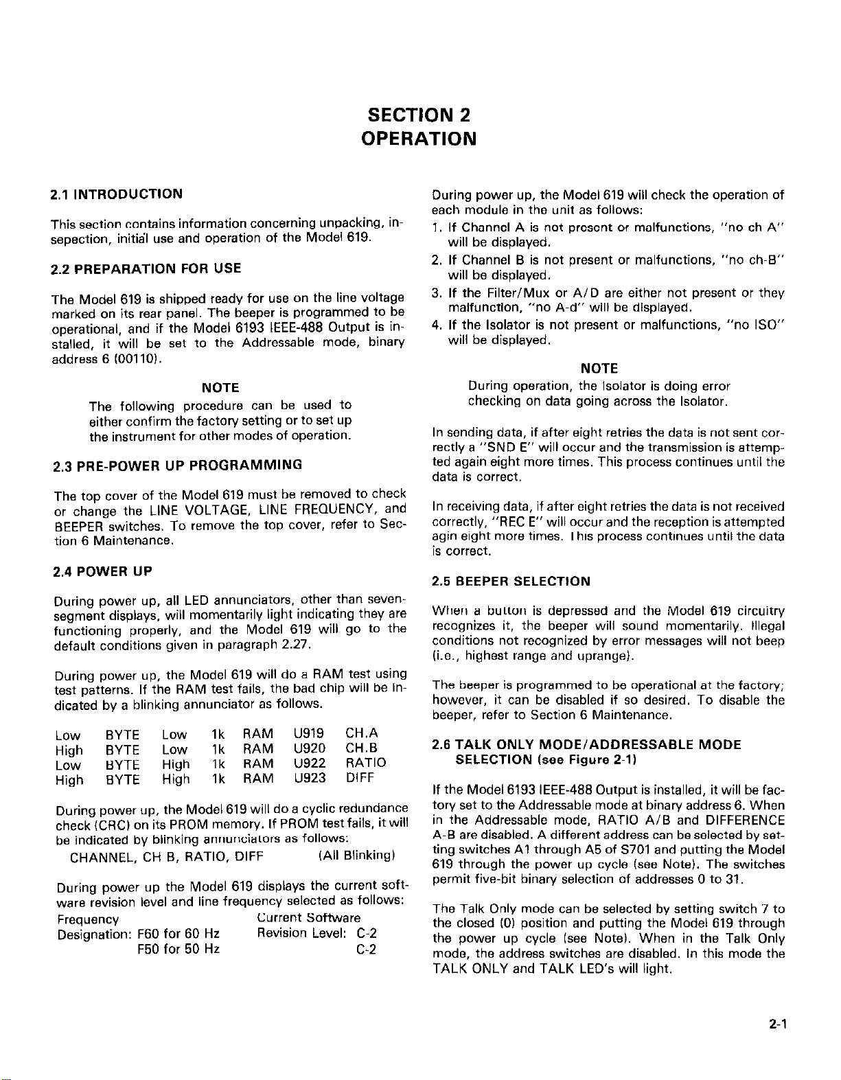
(See Figures 2-1 and 2-2 for front and rear panel detail.)
1.2 FEATURES
The Model 619 includes the following features:
l Resolution of 4% or 5% is standard with the Model 619.
Resolution of 3% is available only when programmed
through the IEEE-488 bus.
l The IEEE-488 Interface option (Model 6193) enables the
Model 619 to be incorporated into a measurement system
that utilizes programmed control through the IEEE-488
bus.
l The modular construction concept allows for future
developement of a line of interfaceable products.
l Whenever two Model 6194 Electrometer Modules are in-
stalled, there are two separate input channels. Channels
A and B measure separately through the READ command
and they are separately switched into the AID Converter.
Channel B is an option.
l Ratio A/B takes a ratio of the two channels, always
dividing A by B.
l Difference A-B subtracts the electrometer value of Chan-
nel B from Channel A.
l A beeper sounds whenever a front panel push-button
switch command is given. The beeper is enabled by
Switch 1 on the Isolator Board.
l The Model 6191 Guarded Adapter, in the guarded switch
position, reduces the effect of additional input cable
capacitance (see paragraph 2.2).
1.3 WARRANTY INFORMATION
The Model 619 and its installed options can be returned to
Keithley for repair and calibration. Also, the Model 619 options (Models 6191, 6193, 6194 and 7008) can be returned
to the factory without the basic Model 619. Information for
returning the Model 619 and/or its options is given on the
inside front cover of this instruction manual.
1.4 MANUAL ADDENDA
Improvements or changes to this manual will be explained
on an addendum attached to the inside back cover.
1.5 SAFETY SYMBOLS AND TERMS
Safety symbols used in this manual are as follows:
The symbol
A
on the instrument denotes that
the user should refer to the operating instructions.
The symbol
IOOOV or more may be present on the terminal(s.1.
‘t
on the instrument denotes that
The WARNING used in this manual explains dangers that
could result in personal injury or death.
The CAUTION used in this manual explains hazards that
could damage the instrument.
1.6 UNPACKING AND INSPECTION
The Model 619 was carefully inspected both mechanically
and electrically before shipment. Upon receiving the Model
619, unpack all items from the shipping container and check
for any obvious damage which may have occured during
transit. Report any damage to the shipping agent. Retain
and use the original packaging materials if reshipment is required. The following items are shipped with all Model 619
orders:
l Model 619 Electrometer/Multimeter with one Model 6194
Electrometer Module and one Model 6011 Triax Input
Cable.
Model 619 Instruction Manual.
Installed or separate optional accessories per request.
Warranty Card(s).
Warranty information is given on the inside front cover of
this instruction manual. If there is a need to exercise the
warranty, contact the Keithley representative in your area to
determine the proper action to be taken. Keithley maintains
service facilities in the United Kingdom and West Germany,
as well as in the United States. Check the inside front cover
of this manual for addresses.
7 SPECIFICATIONS .;
For Model 619 detailed specifications, refer to specifications
that precede this section.
l-l/l-Z
Page 10
SECTION 2
OPERATION
2.1 INTRODUCTION
This section contains information concerning unpacking, in-
sepection, initiil use and operation of the Model 619.
2.2 PREPARATION FOR USE
The Model 619 is shipped ready for use on the line voltage
marked on its rear panel. The beeper is programmed to be
operational, and if the Model 6193 IEEE-488 Output is installed, it will be set to the Addressable mode, binary
address 6 ~001101.
NOTE
The following procedure can be used to
either confirm the factory setting or to set up
the instrument for other modes of operation.
2.3 PRE-POWER UP PROGRAMMING
The top cover of the Model 619 must be removed to check
or change the LINE VOLTAGE, LINE FREQUENCY, and
BEEPER switches. To remove the top cover, refer to Sec-
tion 6 Maintenance.
2.4 POWER UP
During power up, all LED annunciators, other than seven-
segment displays, will momentarily light indicating they are
functioning properly, and the Model 619 will go to the
default conditions given in paragraph 2.27.
During power up, the Model 619 will do a RAM test using
test patterns. If the RAM test fails, the bad chip will be indicated by a blinking annunciator as follows.
LOW
High
LOW
High
During power up, the Model 619 will do a cyclic redundance
check (CRC) on its PROM memory. If PROM test fails, it will
be indicated by blinking annunciators as follows:
During power up the Model 619 displays the current soft-
wars revision level and line frequency selected as follows:
Frequency
Designation: F60 for 60 Hz
BYTE
BYTE
BYTE
BYTE
CHANNEL, CH 9, RATIO, DIFF
LOW lk RAM
LOW lk RAM
High lk RAM U922 RATIO
High lk RAM
F50 for 50 Hz
u919 CH.A
U920 CH.6
U923 DIFF
(All Blinking)
Current Software
Revision Level: C-2
c-2
During power up, the Model 619 will check the operation of
each module in the unit as follows:
1. If Channel A is not present or malfunctions, “no ch-A”
will be displayed.
2. If Channel 6 is not present or malfunctions, “no ch-6”
will be displayed.
3. If the FilterlMux or A/D are either not present or they
malfunction,
4. If the Isolator is not present or malfunctions, “no ISO”
will be displayed.
During operation, the Isolator is doing error
checking on data going across the Isolator.
In sending data, if after eight retries the data is not sent correctly a “SND E” will occur and the transmission is attsmpted again eight more times. This process continues until the
data is correct.
In receiving data, if after sight retries the data is not received
correctly, “REC E” will occur and the reception isattempted
agin eight more times. This process continues until the data
is correct.
2.5 BEEPER SELECTION
When a button is depressed and the Model 619 circuitry
recognizes it, the beeper will sound momentarily. Illegal
conditions not recognized by error messages will not beep
(i.e., highest range and uprangel.
The beeper is programmed to be operational at the factory;
however, it can be disabled if so desired. To disable the
beeper, refer to Section 6 Maintenance.
2.6 TALK ONLY MODE/ADDRESSABLE MODE
SELECTION (see Figure 2-l)
If the Model 6193 IEEE-488 Output is installed, it will be factory set to the Addressable mode at binary address 6. When
in the Addressable mode, RATIO A/B and DIFFERENCE
A-B are disabled. A different address can be selected by setting switches Al through A5 of 5701 and putting the Model
619 through the power up cycle (see Note). The switches
permit five-bit binary selection of addresses 0 to 31.
The Talk Only mode can be selected by setting switch 7 to
the closed 10) position and putting the Model 619 through
the power up cycle lses Note). When in the Talk Only
mode, the address switches are disabled. In this mode the
TALK ONLY and TALK LED’s will light.
“no A-d” will be displayed.
NOTE
2-1
Page 11
Page 12
NOTE
In order for the Model 619 to accept an address or mode change, the instrument must
go through the power up cycle. If the Model
619 is already on, turn it OFF and then back
to ON.
2.7 READING RATE SELECTION
When the Model 619 is in the Front Panel mode and the 5%
digit re$olution mode, two different reading rates can be
chosen via 55 (2.41 rdg/sec) or SE (0.30 rdg/sec). See
Table 2-6. To select the 55 reading rate, refer to Section 6
Maintenance.
2.8 OPERATING INSTRUCTIONS
Table 2-l. Maximum Input
Range
200mV. 2V
Maximum Input
250V RMS, DC to
60Hz sineware
ZnA, 20nA. 200nA
2pA. 20pA. 200pA
ZmA, 20mA
2A
250V RMS, DC to
60Hz sineware
250V RMS, DC to
60Hz sineware,
Fuse Protected
2kn. 20kQ. 200kn
2Mfl. ZOMR, 200M11
ZGO, ZOGQ, 200Gn
2TD
250V RMS, DC to
60Hz sineware
The basic operating instructions for the Model 619 are
outlined in the following paragraphs, Variations and more
complicated measurements will be described later in this
section.
1. The Model 619 is provided with a three-wire line cord
which mates with third-wire grounded receptacles.
WARNING
Ground the instrument through a properly earth-grounded receptacle before
operation. Failure to ground the instrument can result in severe injury or death
in the avant of short circuit or malfunc-
tion. In addition, connect only to the
line voltage selected. Application of
incorrect voltage can damage the in-
strument.
2. Turn on the power by depressing the ON/OFF push button in the lower left-hand corner of the front panel (see
Figure 2.2). Allow one hour for warm up. An additional
hour may be required for temperature extremes. Note
that the rear panel power switch must also be in the ON
position.
3. Upon power up, the Model 619 will go to the default conditions and a beeper will sound for approximately two
seconds, The selected frequency and software revision
level will also be momentarily displayed. To change any
of the default conditions, refer to paragraph 2.27. Input
connectors are located on the rear panel of the Model
6194 Electrometer Module. The main input is in the triax
connector, with a separate input for the 2 Amp range. An
Analog Output is provided for convenience on a DIN con-
nector (refer to Figure Z-21. Connect the measurement
source to the input terminals and make the desired
measurement. See Table 2-l for maximum input.
2.9 FRONT PANEL FUNCTIONS
The Model 619 Front Panel has two funCtiOnal groups. an
Annunciator and Display Group and a Function Saiectqr
Group. See Figure 2-2.
2.9.1 Annunciator and Display Group
The software or manually selected status of the Model 619
may be determined at any time by looking at the Annunciators. There are four Annunciator Groups; Status Blocks
A, B, C and D.
1. Status Block A indicates the channel status as either
Channel A, Channel B, Ratio A/B, or Difference A-B.
2. Status Block B indicates the status of other functions including,
Zero Check, Suppression, Auto Range, Filter,
Trigger, Update, and External Feedback.
,3. Status Block C indicates the IEEE-488 bus status as
Remote, Listen, Talk, SRQ, Binary, Talk Only, or LLO.
4. Status Block D indicates the measurement; Volts, Amps,
or Ohms.
The E-Digit Display next to Status Block D indicates the
measured value, power, and sign of the input to the Model
619 ElectrometeriMultimeter. In addition to these Status
Blocks, status may also be determined by controller sampling through the IEEE-488 bus.
2.9.2 Function Selector Group
The Function Selector Group consists of seven blocks; Dual
Channel including Ratio and Difference, Volts-Amps-Ohms,
Range Selection, Zero Controls, Baseline Controls, Filter,
and Resolution.
NOTE
Note that all front panel operations described below, except Ratio and Difference, may
be programmed or controlled from the
IEEE-488 bus using the optional Model 6193
Interface. In Remote (or Manuall mode, the
Model 619 front panel selector push-button
switches are active unless LLO is commanded through the bus.
2-3
Page 13
2.9.3 Dual Channel
Whenever the Model 619 has a second Model 6194 Elec-
trometer Module installed, Channel A or B may be selected
from the front panel or bus. The two channels are independent so that they operate as two separate instruments and
can be separately programmed.
1. Channel A
A. Upon power up of the Model 619, CHANNEL A will be
displayed in the Channel Status Block.
B. Otherwise, depressing the CHANNEL A push button
will:
(a) Display CHANNEL A data.
lb) Light the CHANNEL A annunciator.
2. Channel B
A. Depressing the CHANNEL B push button will:
(a) Display CHANNEL B data.
(b) Light the CHANNEL B annunciator.
B. If there is no Channel B installed in the Model 619,
depressing the CHANNEL B push button will:
la) Display the error message “no ch-b.”
(b) ReIeit-: the Model 619 to the previous operating
3. Ratio A/B and Difference A-B. In any Function or Range
the Ratio or Difference between Channel A and B, from
10-1s to IOf’s, may be calculated and displayed.
NOTE
The Model 6193 IEEE-488 Interface must be
in the Talk Only mode or else not installed
for Ratio and Difference operations.
1. Light the DIFFERENCE A-B annunciator.
2. Take one reading at 4.8rdglsec rate on Channel
A.
3. Take one reading at 4.8rdglsec rate on Channel
B.
4. Compute the difference.
5. Display the difference at a 2.4rdg/sec rate, with
a 5%.digit resolution.
6. Repeat the above seauence.
(c) If there is no Channel B installed, depressing the
DIFFERENCE A-B push button will:
1, Display the error message “no ch-b.”
2. Return to the previous operating mode.
NOTE
Observe that the largest value that can be
displayed in the Ratio or Difference mode is
1999.99 x 10’s. The smallest value that can
be displayed is 0.00000 x 10⁻¹s. Any time a
division by zero is attempted, the display
message is “OFLO” (overflow). The data
used internally by the Model 619 is to a
higher resolution than the displayed reading.
Therefore, a display of all zeros on Channel
B will not necessarily result in a RATIO
“OFLO.”
2.9.4 Volts, Amps, and Ohms
Volts, Amps.
or
Ohms functions may be manually selected
for a wide range of measurements. Programmed or software selected may also be obtained through the IEEE-488
Interface bus.
A. Ratio A/B
(a) If the Model 819 is in the Addressable mode, the
RATIO A/B command is locked out and cannot be
selected.
(b) Otherwise, when the RATIO A/B push button is
depressed the Model 619 will:
1. Light RATIO A/B annunciator.
2. Take one reading at 4.8rdglsec rate on Channel
A.
3. Take one reading at 4.8rdg/sec rate on Channel
B.
4. Compute the ratio.
5. Display the ratio at 2.4rdg/sec rate with 5% digit
resolution.
6. Repeat the above sequence.
(c) If there is no Channel B installed. deoressing the
RATIO A/B push button will:
1. Display the error message “no ch-b.”
2. Return to the previous operating mode.
B. Difference A-B
(a) If the Model 619 is in the Addressable mode, this
command is locked out and cannot be selected.
(b) Otherwise, when the DIFFERENCE A-B push but-
ton is depressed the Model 619 will:
NOTE
In resistance and voltage modes, analog output is noninverted and can be used for
guarding.
I. Volts
A. Upon oower up the Model 619 will go to the Volts
function.
B. If the Model 619 is in the Ratio A/B or the Difference
A-B mode, this command is locked out and cannot be
selected.
C. Otherwise, selecting the Volts function for the
rently displayed channel will:
(a) Light the VOLTS annunciator.
(b) Program the Electrometer for the Volts function.
2. Amps
A. If the Model 619 is in the Ratio A/B or the Difference
A-B mode, this command is locked out.
B. Otherwise, selecting the Amps function for the cur-
rently displayed channel will:
(a) Light the AMPS annunciator.
(b) Program the Electrometer for the Amps function.
cur-
2-4
Page 14
3.
Ohms
A. If the Model 619 is in the Ratio A/B or the Difference
A-B mode, this command is locked out.
B. Otherwise, selecting the Ohms function for the cur-
rently displayed channel will:
(a) Light the OHMS annunciator.
(b) Program the Electrometer for the Ohms function.
2.9.5 Range Selection
1. Auto/Manual
A. Auto or manual range may be selected by pressing
the appropriate front panel button or by programming
on the Interface bus.
8. If the Model 619 is in the Ratio A/B or the Difference
A-B mode, this commend is locked out.
C. If the channel currently being displayed is in AUTO
RANGE. deoressina the AUTO/MANUAL oush button will:’ (a) Turn off the AUTO RANGE annunciator.
(b) Place Model 619 into Manual Ranging.
(4 Then hold the present range.
D. If the channel currently being displayed is in Manual
Ranging, depressing the AUTO/MANUAL push button will:
(al Light the AUTO RANGE annunciator.
(b) Begin Auto Ranging.
(cl Hold the previously displayed reading until settled
range is found, then display it.
E. The following ranges cannot be accessed in the Auto
Range mode and actuation of Auto/Manual in any of
these function range combinations will result in an
error display of “noAU”:
(a) 2 Amp Range. This range requires a separate
input.
(b) External Feedback (Amps Function).
(4 2G Ohm through 2T Ohm Range. These high
resistances require long time constants.
2. Uprange/Downrange. Manual ranges are advanced up or
down by pressing the appropriate front panel button. The
desired range may also be programmed on the Interface
bus.
A. Uprange
(a) If either RATIO A/B or DIFFERENCE A-8 is
selected, this command is locked out and cannot
be accomplished.
(b) If the channel currently being displayed is in
AUTO RANGE, depressing the UPRANGE button
will place the Model 619 is Manual Ranging and
advance Uprange one step.
(c) If the channel currently being displayed is in
MANUAL RANGE, depressing the UPRANGE
push button will advance Uprange one step.
(d) If the channel currently being displayed is in
MANUAL RANGE and on the highest possible
range for that function, depressing the UPRANGE
push button will be ineffective.
B. Downrange. Downrange operates in the same manner
as Uprange.
C. External Feedback. External Feedback is accessible on
Amps function by touching or programming
UPRANGE on the 2 Amp range.
(a) If the displayed channel is in AMPS and Range 20
(range above the 2 Amp range), the Model 619
will:
1. Place the Electrometer in the Ext Feedback
mode.
2. Light the EXT FEEDBACK annunciator.
(b) All status which were in effect for Range 8 in
AMPS are in effect for EXT FEEDBACK.
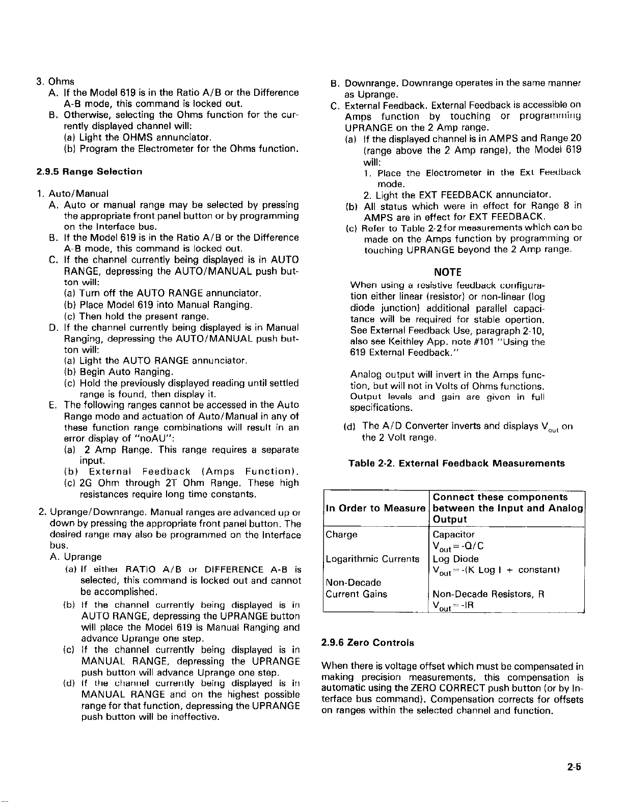
(c) Refer to Table 2-2for measurements which can be
made on the Amps function by programming or
touching UPRANGE beyond the 2 Amp range.
NOTE
When using a resistive feedback configura-
tion either linear (resistor) or non-linear (log
diode junction) additional parallel capacitance will be required for stable opertion.
See External Feedback Use, paragraph 2.10,
also see Keithley App. note #IO1 “Using the
619 External Feedback.”
Analog output will invert in the Amps func-
tion, but will not in Volts of Ohms functions.
Output levels and gain are given in full
specifications.
(d) The AID Converter inverts and displays Vout on
the 2 Volt range.
Table 2-2. External Feedback Measurements
Connect these components
In Order to Meawn
between the Input and Analog
Output
Capacitor
V,,t = -Q/C
Logarithmic Currents
Log Diode
V O,,t= -lK Log I + constant)
Current Gains
2.9.6 Zero Controls
Non-Decade Resistors, R
=-IR
V
wt
!
When there is voltage offset which must be compensated in
making precision measurements, this compensation is
automatic using the ZERO CORRECT push button (or by Interface bus command). Compensation corrects for offsets
on ranges within the selected channel and function.
2-5
Page 15
1. Zero Check
A. If the displayed Channel (A or B) is not currently in
ZERO CHECK, depressing the ZERO CHECK push
button will:
(a) Program the Electrometer to Zero Check.
(b) Light the ZERO CHECK annunciator.
B. If the displayed Channel (A or B) is currently in ZERO
CHECK, depress the ZERO CHECK push button, and
the Model 619 will:
(al Turn off ZERO CHECK annunciator.
(b) Program the Electrometer out of Zero Check.
C. If the displayed channel is in AMPS, Range 9,
depressing the ZERO CHECK push button will display
the error message “no 2AC” (no Zero Check in 2 Amp
range).
2. Zero Correct
A. If either RATIO A/B or DIFFERENCE A-B is selected,
this command is locked out and cannot be
accomplished.
8. If the Model 619 is not in ZERO CHECK or is 2 Amp
current range, depressing the ZERO CORRECT push
button will:
(a) Display the error message “corr IL”
(b) Then return to the previous operating mode.
C. If the Model 619 is in ZERO CHECK, depressing the
ZERO CORRECT push button will:
(a) Disable the filter.
(b) Put the AID Converter in times 10 gain mode and
in a 16.66msec integration period.
(cl Average 2 conversions.
(d) Take a reading with the Electrometer attenuator in
- 1 and then - 10.
(a) Solve for Electrometer and A/D offsets.
(f) Repeat above steps for IOOms integration time
period.
(g) Return to previous operating mode in Zero Check,
compensating for all internal voltage offsets
measured during Steps a through f.
2.9.7 Baseline Controls
(a) Store the current reading in the Baseline register
assigned to the currently displayed Channel/Function. There are six Baseline registers: Channel
A/Volts, Channel A/Amps, Channel A/Ohms,
Channel B/Volts, Channel B/Amps, and Channel
B/Ohms.
fb) If in Baseline Suppression mode, take unit out of
Baseline Suooression. which will turn off the
BASELINE SUPPRESSION annunciator.
fc) Return to previous operating mode (except
Baseline Suppression).
2. Baseline Suppression
A. If either RATIO A/B or DIFFERENCE A-B is selected,
this command is locked out.
If the Model 619 is not currently in the Baseline
Suppression mode, depressing the BASELINE SUPPRESSION push button will:
(a) Light the BASELINE SUPPRESSION annunciator.
tb) Subtract from display the contents of the ap-
propriate Channel/Function Baseline register
(e.g., if 0.10 volts is stored in the Channel B/Volts
Baseline register, subtract 0.10 Volts from
readings on all Channel B voltage ranges).
If the Model 619 is currently in the Baseline Suppres-
sion mode, depressing the BASELINE SUPPRES-
SION push button will:
Ia) Take unit out of Baseline Suppression.
lb) Turn off the BASELINE SUPPRESSION annun-
ciator.
WARNING
If the Model 619 is in the 200 Volt range
and in Basline Suppression, the
BASELINE SUPPRESSION annunciator
will blink indicating a safety warning. A
dangerous voltage level could exist and
still be read es a lower voltage as
displayed by the instrument. This could
present a shock hazard should the
operator misinterpret the measurement
relative to actual voltage.
Baseline Controls assist in making relative measurements es
referenced to a known value (leakage, operating
parameters, etc.). The Model 619 will subtract this amount
on all ranges on the particular channel where a baseline is
assigned.
WARNING
The Suppression light will blink on the
200 Volt range, indicating e possible
high voltage safety hazard.
1. Baseline Store
A. If either RATIO A/B or DIFFERENCE A-B is selected,
or the instrument is currently displaying “OFLO,” this
command is locked out and cannot be accomplished.
B. Otherwise, depressing the BASELINE STORE push
button will:
2-6
2.9.8 Filter
When the Filter is placed in operation, by pressing the
FILTER push button or commanding it through the
IEEE-488 Interface bus, an additional 25dB of line frequency
rejection filtering is applied.
1. If either RATIO A/B or DIFFERENCE A-B is selected, this
command is locked out.
2. If the displayed channel is not currently in the Filter
mode, depress the FILTER push button and the Model
619 will:
A. switch the Filter in.
B. Light the FILTER annunciator.
3. If the displayed channel is currently in the Filter mode,
depressing the FILTER push button will:
A. Switch the Filter out.
B. Turn off FILTER annunciator.
Page 16
2.9.9 Resolution
Pressing the RESOLUTION push button provides an extra
decade of sensitivity and resolution. This may also be ac-
complished, by command, on the IEEE-488 Interface bus.
NOTE
For example, the 2nA range, in Resolution,
will go from 4% digit, 100Fa. Isd, to 5%
digit, 1OfA Isd resolution. Noise is typically a
few digits in the fifth place.
1. If either RATIO A/B or DIFFERENCE A-B is selected, this
command is locked out.
2. If the Model 619 is currently displaying the 4% digits,
depressing the RESOLUTION push button will:
A. Reduce the reading rate to 2.4rdg/sec.
B. Increase the display resolution to 5% digits.
3. If the Model 619 is currently displaying 5% digits,
depressing the RESOLUTION push button will:
A. Increase the reading rate to 5,49rdg/sec.
B. Reduce the display resolution to 4% digits.
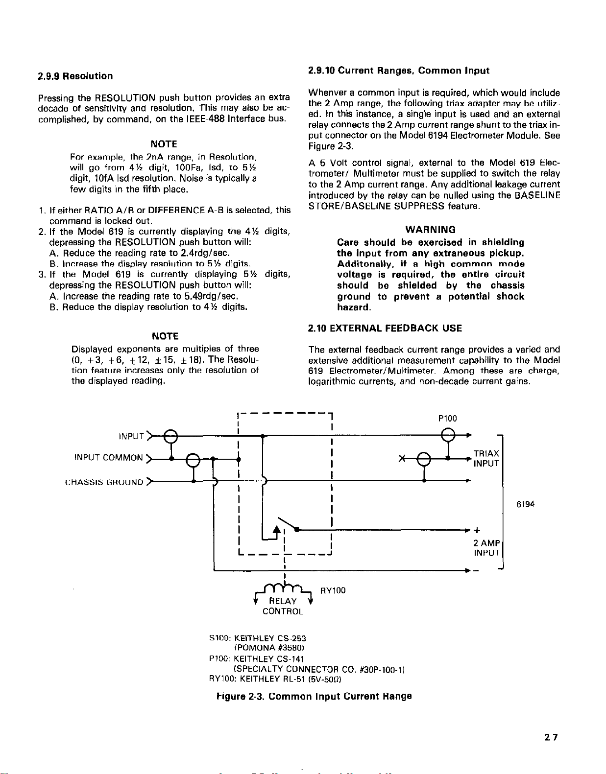
2.9.10 Current Ranges, Common Input
Whenver a common input is required, which would include
the 2 Amp range, the following triax adapter may be utilized. In this instance, a single input is used and an external
relay connects the 2 Amp current range shunt to the triax input connector on the Model 6194 Electrometer Module. See
Figure 2-3.
A 5 Volt control signal, external to the Model 619 Electrometer/ Multimeter must be supplied to switch the relay
to the 2 Amp current range. Any additional leakage current
introduced by the relay can be nulled using the BASELINE
STORE/BASELINE SUPPRESS feature.
WARNING
Care should be exercised in shielding
the input from any extraneous pickup.
Additonally, if a high common mode
voltage is required, the entire circuit
should be shielded by the chassis
ground to prevent a potential shock
hazard.
NOTE
Displayed exponents are multiples of three
(0, *3, i6, *12, *15, *181. The Resolu-
tion feature increases only the resolution of
the displayed reading.
I- -
I
I
INPUT COMMON >
CHASSIS GROUND >
*-
+
. \
,
I
------
I
&
CONTROL
2.10 EXTERNAL FEEDBACK USE
The external feedback current range provides a varied and
extensive additional measurement capability to the Model
619 Electrometer/Multimeter. Among these are charge,
logarithmic currents, and non-decade current gains.
1
PlOO
I
I
I
I
TRIAX
INPUT
I
I
6194
2 AMP
INPUT
RYlOO
5100: KEITHLEY es-253
(POMONA #358Ol
PlOO: KEITHLEY CS-141
(SPECIALTY CONNECTOR CO. #3OP-100.11
FlYlOO: KEITHLEY AL-51 (5V-500)
Figure 2-3. Common Input Current Range
2-7
Page 17
The input circuitry used in the Model 6194 Electrometer in
the Amps function is configured in the feedback Amps
mode as illustrated in Figure 2-4. An input currant applied at
the negative input of the op amp is nulled with a current
through the parallel combination of R,, ,and C,, from the
output of the op amp. This is accomplrshed by the high
open-loop gain (typically greater than 40,000) of the op amp
which holds its negative input at virtual ground (its positive
input which is connected to input common). R,, in parallel
with C,, converts the input current to a voltage which is further processed by the AID Converter in the Model 619.
Included in this processing is a reinversion of the signal
polarity to match that of the actual input.
parallel combination of the two quantities separated by
this symbol (AlI B)=AB/fA + Bl).
5. Selection of the external feedback network must incorporate the proper frequency compensation required by
the Model 6194 Electrometer Module.
6. All external feedback circuitry should be housed in a
suitably shielded enclosure. Insulators supporting the input node (input HII should be constructed of Teflon@
or
other high quality insulator.
2.10.1 External Trigger
When the Model 619 is turned on it is in the continuous
mode To. When switch S3 (Figure 6-1, Isolator Board) is
switched to ON and the, Resolution button is pressed the
Model 619 is placed into the one shot mode Tl. The Tl
mode allows a trigger only from the front panel by pressing
the Ratio/Difference button or by the External Trigger.
The external trigger requires a falling edge pulse at TTL logic
levels. The trigger voltage should be between, greater than
Or equal to zero, and less than or equal to + 5 volts. The external trigger pulse initiates a measurement conversion, For
one shot (Tl, T3 and T5) times (trigger to first byte) refer to
Table 2-8. For continuous ITO, T2 and T4) times refer to
Table 2-7.
Figure 2-4. Model 6194 Electrometer Input Circuitry
The availability of the analog output permits the user to
substitute an external network for the combination of
R ,and C,,. In effectively applying the capability, a number
o F factors must be taken into account.
1. The total absolute value current supplied by the analog
output for both feedback to the input and monitoring of
the analog output must be less than 22mA.
2. The Model 619 processes the Model 6194 Electrometer
output as a i2.OOOOVDC f *2.00000VDC in the 5%
digit mode) signal correctly inverting the polarity for an
accurate representation of the input signal polarity. This
output voltage is the level impressed across the external
feedback network.
3. Accuracy of the response is the same as that for the 2
Volt range, excluding the contribution of all user-supplied
external feedback circuitry. Noise and NMRR will also be
a function of this external circuitry.
4. Input impedance is given by the relationship
z - 0.5MD 11 (Z /A ), where ZFB is the external feedb!!ckietwork and xv is”tha open-loop gain of the op amp
(typically greater than 40,000). Note that in Zero Check,
A” is reduced to unit” Ill and that /I represents the
NOTE
The external trigger is inhibited in the SO
mode or by LLO (local lockout).
Electrometer Complete-The Electrometer Complete output
is a 400~s~ wide positive pulse that signifies completion of
the measurement conversion cycle. The Electrometer Complete line can be used to trigger another instrument or to in-
form an instrument that the measurement conversion cycle
has been completed.
For example: The Model 619 can be used with a scanner.
The Electrometer Complete line can trigger the scanner to
switch to the next available channel when the Model 619
measurement cycle has been completed.
2.10.2 Charge
The measurement of charge can be made directly by using
an external feedback capacitor, C,,, as illustrated in Figure
2-6. In the relationship Cl= CV, Q= charge (coulombs) applied to input, C=capacitance (farads) of Cr. and
V= voltage (volts) at output as indicated on the display. The
Model 619 display will read charge directly in the units determined by C. For example, using IpF capacitor will provide a
display in pC.
In practice, C,, should be greater than 1OOpF for feedback
stability and of a suitable dielectric material to ensure low
leakage and low dielectric absorption. Polystyrene and
2-g
Page 18
polypropylene dielectric capacitors offer good performance
in this regard.
As shown in Figure 2-5 an external Zero Check contact may
be desirable in certain applications where 0.5MQ Zero Check
input impedance cannot be tolerated. R,,,,, protects this
contact from the discharge surge of C, Care should be ax
ercised in the selection of this contact switch or relay) that
a
the high impedance, low current requirements of the circuitry are not compromised.
From this equation, proper selection of transistor 01 (Figure
2-6) would require a device with a high current gain (h,,)
which is maintained war a wide range of emitter currents.
Suitable devices include Analog Devices AD812 and Precision Monolithics MAT-Ql.
Frequency compensation/stabilization is accomplished by
C,,. Selection of a proper value depends on the particular
transistor being used and the maximum current level anticipated. Compensation at the maximum current is required
since the dynamic impedance of the transistor will be a
minimum at this point. It should be noted that the response
speed at lower currents will be compromised due to the increasing dynamic impedance.
Z (impedance) = 2V/21= kT/ql=O.O26/1 @25OC
Using the MAT-01 or AD818, a minimum RC time constant
of 50@ec at maximum input current should be used. At
I,,(maxl of 100/1A, this would correspond to 0.2pF. Note
that at lOOnA, this would increase the RC response time
constant to 50msec (5sec at InAl. A minimum capacitance
of IOOpF is recommended.
Figure 2-5. Charge Measurement
2.10.3 Logarithmic Currents
The use of a diode junction in the external feedback path
permits a logarithmic current-to-voltage conversion. This
relationship for a junction diode can be given by the
equation:
V=m kT/q In (I/lol+lR,
where q = unit charge (1.6022x10-‘90, k= Boltzmann’s
constant ~1.3806x10-*~J/°Kl, and T= Temperature (OK).
The limitations in this equation center on the factors I,,, m,
and Rs. lo is the extrapolated current for V=O. An empirical
proportional constant, m, accounts for the different
character of currant conduction (i.e. recombination and
diffusion) mechanisms within the j&ion, typically varying
in value between 1 and 2. Finally, R, constitutes the ohmic
bulk resistance of the diode junction material. lo and Rs limit
the usefulness of the junction diode as a log converter at
low and high currants, respectively. The factor m introduces
non-linearities between these two extremes. With all these
factors taken into account, most diodes have a limited range
of useful logarithmic behavior.
A solution to these constraints is the use of a transistor configured as a “transdiode” in the feedback path as shown in
Figure 2-6. Analyzing the transistor in this configuration
leads to the relationship:
V= kT/qllnl/lo-In (h&(1 + h,,)ll
where H,, is the current gain of the transistor.
Although the input to this configuration is a current source,
a voltage source can be used with a suitable ballast resistor.
In this configuration, the input burden of ImV must be considered as an error s~ource against the input voltage.
Further processing of the response can be accomplished
with Baseline Suppression and Ratio. Baseline Suppression
provides an offset and Ratio provides a scaling factor (with
optional Channel B, Model 6194 Electrometer Module installedl. Alternately, a controller (computer) can process the
data via the IEEE-488 bus output (with optional Model 6193
IEEE Interface installed).
Figure 2-6. Logarithmic Current Measurement
2.11 NON-DECADE CURRENT GAINS
The Model 6194 Electrometer uses internal decade
resistance feedback networks for the 2nA through 20mA
currant ranges. In some applications a non-decade currentto-voltage conversion (gain) may be desirable. As illustrated
in Figure 2-7 a calibratable resistance, R,,, serves this purlXXe.
2-9
Page 19
not in the remote mode, the first arguments preceding
the remote mode will not program the Model 619 and will
cause “NO rN” to be displayed. The Model 619 front
panel push-button switches will respond unless LLO is
commanded through the bus. Pressing the RATIO button
initiates a conversion(s) if a trigger is being awaited by
the Model 619 (the RATIO button is a manual trigger dur-
ing bus operation). After programming, the front panel
does not reflect the new configuration until the Model
619 is triggered.
Table 2-4. Secondary Address
Figure 2-7. Non-Decade Current Gain Measurement
Limitations on the value of R,, require it to be in the range
of 102n to 10’00. Frequency compensation/stabilization is
accomplished by C,,. Selection of C,, based on an RC
response time should be per Table 2-3 with a minimum value
of IOOpF:
TABLE 2-3 C,, SELECTION
2.12 SYSTEM OPERATION (Using the Model 6193
IEEE-488 Interface)
2.13 ADDRESS SELECTION
1. Primary Address. The Primary Address of the Model 619
is selected by 5 switches on the IEEE-488 module (see
Figure 2-l). These switches are accessible from the rear
panel of the unit. This allows the selection of 31 primary
listener/talker address pairs. Binary 11111 is reserved for
the Untalk and Unlisten commands.
2. Secondary Address. The Model 619 uses a secondary
addressing to distinguish between SRQ requests, commands and data associated with input Channel A and input Channel B. To address the Model 619, the IEEE-488
controller must send the primary address of the Model
619 followed by the secondary address of the desired
channel. See Table 2-4 for secondary addresses.
2.14 BUS MANAGEMENT LINES
FUNCTION
Channel A (LISTEN)
ASCII HEX
a
1
;;”
Channel A (TALK)
Channel B (LISTEN)
Channel B (TALK1
SRQ (TALK)
Status Request A (TALK)
Status Request El (TALK) ii 64;
i 62;
b
f 3
63H
-I
2. Interface Clear (IFC). Clears the Interface and goes to
talker/listener idle states. There are no state (function,
range, etc.) changes in the Model 619.
3. Service Request (SRQ). Requests serial poll service.
4. End (EOII. Asserted during last byte of multi-byte data
transfer.
5. Attention (ATN). Asserted when address or commands
are present on the bus.
2.14.1 Bus Commands Implemented
1. Universal Commands
A. Device Clear (DCL). The Model 619 goes to default
conditions (see paragraph 2.27)
B. Local Lock Out (LLOI. If LLO is given, the front panel
controls cannot cause a change in status in the Model
619. (The LLO annunciator will light when in LLO).
C. Serial Poll Disable (SPD). Disables serial polling.
D. Serial Poll Enable (SPE). When addressed to Talk, the
Model 619 will send the SRQ status word.
E. Untalk (UNTI. Puts the Model 619 into a talker idle
state if it was a talker.
F. Unlisten (UNLI. Puts the Model 619 into a listener idle
state if it was a listener.
1. Remote Enable (REN). To place the Model 619 into the
remote mode, send REN and the appropriate listen ad-
dress and the remote indicator will light. The statement
used to enter the remote mode (i.e. REN end Address)
must not contain any other commands. The Model 619
must be in the remote mode to be programmed. If it is
2-10
2. Address Commands
A. Selected Device Clear (SDC). If the Model 619 is ad-
dressed to listen it will go to default conditions.
B. Group Execute Trigger (GET). If the Model 619 is ad-
dressed to listen and in the proper trigger mode (T2 or
T3). it will automatically trigger a conversion.
Page 20
2.14.2 Input Channel Control (Secondary Address is a
or bl
1. Channel. Input Channels A and B can be separately ad-
dressed and controlled using secondary addressing. Each
input channel has several internal status words which
define the current operating status of the channel. When
addressed to Talk, the status words define the function,
range, and mode of operation by which the data will be
accepted. The status words can be modified by the
following device dependent commands sent via the bus
(see Status Section). In order to program Channel A or
Channel 8 the machine must be in Remote mode.
2. Device Dependent Commands. The following device
dependent commands apply to either Channel A or
Channel B as defined by the secondary address. Any or
all may be used followed by an execute command “X” to
inititate the change. Only after the execute command
will the change take place. Commands may also be sent
in sections, for example:
First Commands Send Fl
Second Command Send R2X
The above commands are the same as sending Fl R2X in
one command.
A. Function and Range. Refer to Tables 2-5 and 2-6 for
function and range information.
B Bus Response Mode
(a) Mg Standard. On error or data, the Model 619 will
not access SRQ (status byte will still contain up-
to-date information if serial poll done).
(b) Ml Interrupt. On error or data, the Model 619 will
access SRQ when appropriate.
(c) Pwr ON/DCL/SDC, Default Mid.
C. Trigger Mode (same for both Channels A and B)
(a) T@ Continuous on Talk. The Model 619 con-
tinuously updates the display at the programmed’
reading rate after being address to Talk. The output data buffer will be updated at the same rate as
the display if the data is read out at the same rate.
If the data is not read out, the reading will be held
in the output data buffer until it is read out. When
it is read out, the next value will then be placed in
the buffer.
(b) Tl One-Shot on Talk. The Model 619 will update
the output data buffer at the programmed rate,
once each time a conversion is initiated by being
addressed to Talk (to retrigger, address to Talk
again) (see Figure 2-B).
(c)
T2 Continuous on GET. The same as Continuous
on Talk except it is done on GET (see Figure 2-B).
(d) T3 One-Shot on GET. After a GET command is ac-
cepted by the Model 619, it will initiate a conversion. The Model 619 will update the output data
buffer once at the oroarammed reading
rate (see
Figure 2-B).
(a) T4 Continuous on X. The same as Continuous on
Talk except it is done on X (see Figure 2-B).
(fl T5 One-Shot on X. After an “X” command is
accepted by the Model 619, it will initiate a conversion. The Model 619 will then update the output
data buffer once at the programmed reading rate
(see Figure 2-81.
(g) Pwr ON/DCL/SDC, Default T@.
Table 2-5. Function
I
Power ON/DCL/SDC, Default F@
Table 2-6. Range
Volts
Auto
200mV
2v
2ov
2oov
*2oov
l
2oov
l
2oov
*2oov
2oov
l
2oov
__IN/DC
Amps
Auto
2nA
20nA
200nA
W
20fiA
2OOfiA
2mA
20mA
l
2Amps
**EXT FEEDBACK
I
SDC, Default R4
Ohms
Auto
2k
20k
200k
2M
20M
200M
“2G
“20G
200G
“2T
*Will not autorange into these ranges
**EXT FEEDBACK is considered to be an Amps range and
not an individual function.
2.15 DATA FORMAT
1. D@ ASCII Data String. The internal Model 619 priorities
are such that ASCII data is passed to the interface after the
display is updated (same for Channels A and 6).
2. Dl Binary Data String. The internal Model 619 priorities
are such that Binary data is passed to the interface before
going to the display. The display will be blank except for
bus annunciators.
2.16 ASCII FORMAT
Channels A and B can be separately addressed to talk using
secondary addresses a and b. When the Model 619 is addressed to Talk, it will transmit the current contents of its
output data buffer as a 16 to 18 byte ASCII string. The actual length of the ASCII string depends
on
the
number
of
programmed terminators. Refer to Figures 2-9 and 2.10 and
Tables 2-7 through 2.9.
2.17 BINARY FORMAT (Refer to Figure 2-11)
1. In the binary data mode, the Binary annunciator will turn
ON and the display becomes blank except for the bus an-
nunciators.
2-11
Page 21
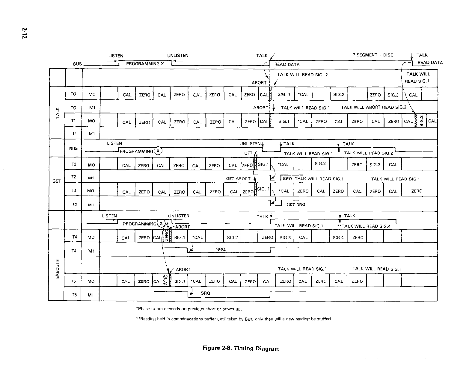
Figure 2-8. Timing Diagram
Page 22
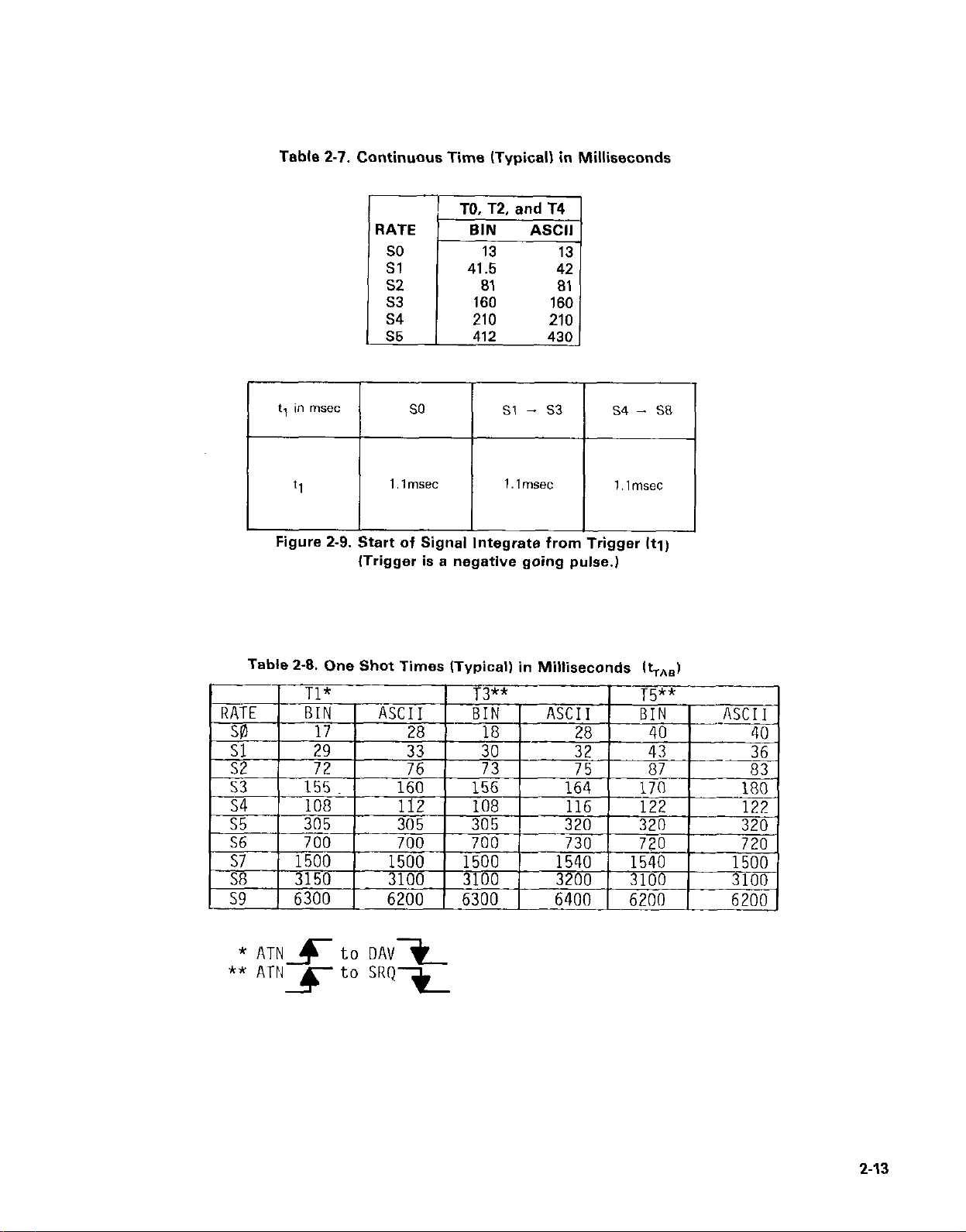
Table 2-7. Continuous Time (Typical1 in Milliseconds
RATE
SO
Sl
S2
S3
s4
s5
t) in m*ec 1
I
SO
Sl -
I
s3 I
54 - SE
L
Figure 2-9. Start of Signal Integrate from Trigger Itl)
(Trigger is a negative going pulse.)
Table 2-8. One Shot Times ITypical) in Milliseconds I%,,)
I
I
* ATNxto DAVX
** ATN
to SRQ
5 7L
z-13
Page 23
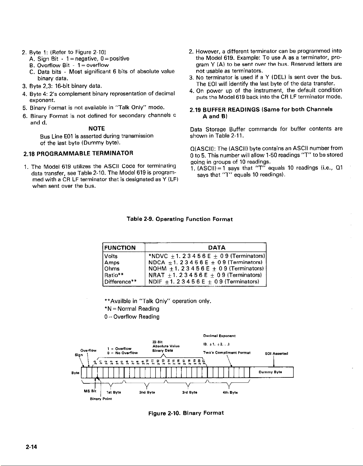
2. Byte 1: (Refer to Figure 2-10)
A. Sign Bit - 1 = negative, 0 = positive
B. Overflow Bit 1 =overflow
C. Data bits Most significant 6 bits of absolute value
binary data.
3. Byte 2,3: 16-bit binary data.
4. Byte 4: 2’s complement binary representation of decimal
exponent.
5. Binary Format is not available in “Talk Only” mode.
6. Binarv Format is not defined for secondary channels C
Bus Line EOl is asserted during transmission
of the last byte (Dummy byte).
2.18 PROGRAMMABLE TERMINATOR
1, The Model 619 utilizes the ASCII Code for terminating
data transfer, see Table 2.10. The Model 619 is program-
med with a CR LF terminator that is designated as Y (LFI
when sent over the bus.
Table 2-9. Operating Function Format
2. However, a different terminator can be programmed into
the Model 619. Example: To use A as a terminator, pro-
gram Y IA) to be sent over the bus. Reserved letters are
not usable as terminators.
3. No terminator is used if a Y (DEL) is Sent over the bus.
The EOI will identify the last byte of the data transfer.
4. On power up of the instrument, the default condition
puts the Model 619 back into the CR LF terminator mode.
2.19 BUFFER READINGS Wnne for both Channels
A and Bl
Data Storage Buffer commands for buffer contents are
shown in Table 2-11.
Q(ASCII): The (ASCII) byte contains an ASCII number from
0 to 5. This number will allow l-50 readings ‘7” to be stored
going in groups of 10 readings.
I, (ASCII) = 1 says that ‘7” equals 10 readings (i.e., 01
says that “T” equals 10 readings).
FUNCTION DATA
Volts
Amps
Ohms
Ratio**
Difference**
““Availble in “Talk Only” operation only.
*N = Normal Reading
0 = Overflow Reading
*NDVC * 1. 2 3 4 5 6 E f 0 9 (Terminators)
NDCA i- 1. 2 3 4 5 6 E + 0 9 (Terminators)
NOHM + 1. 2 3 4 5 6 E + 0 9 (Terminators)
NRAT f 1. 2 3 4 5 6 E f 0 9 (Terminators)
NDIF + 1. 2 3 4 5 6 E f 0 9 (Terminators)
Figure 2-10. Binary Format
7
2-14
Page 24
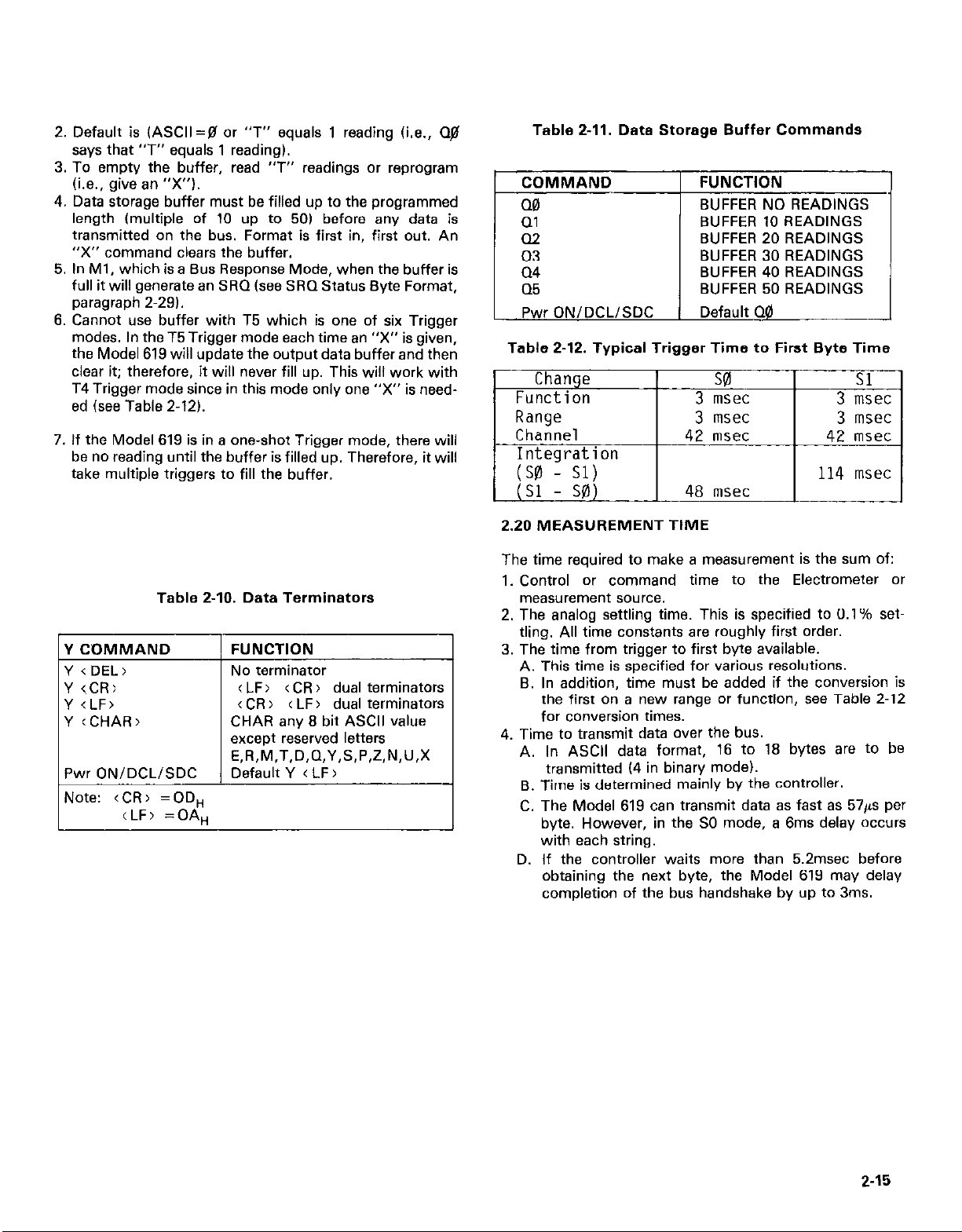
2. Default is (ASCII=@ or “T” equals 1 reading (i.e., Qa
says that “T” equals 1 reading).
3. To empty the buffer, read “T” readings or reprogram
(i.e., give an “X”).
4. Data storage buffer must be filled up to the programmed
length (multiple of 10 up to 501 before any data is
transmitted on the bus. Format is first in, first out. An
“X” command clears the buffer.
5. In Ml, which is a Bus Response Mode, when the buffer is
full it will generate an SRQ (see SRQ Status Byte Format,
paragraph 2-29).
6. Cannot use buffer with T5 which is one of six Trigger
modes. In the T5 Trigger mode each time an “X” is given,
the Model 619 will update the output data buffer and then
clear it; therefore, it will never fill up. This will work with
T4 Trigger mode since in this mode only one “X” is needed (see Table 2-12).
7. If the Model 619 is in a one-shot Trigger mode, there will
be no reading until the buffer is filled up. Therefore, it will
take multiple triggers to fill the buffer.
Table 2-10. Data Terminators
except reserved letters
E.R.M.T.D.Q.Y.S.P.~.N.U.X
Pwr ONIDCLISDC Default Y ( LF)
Note: <CR, =QD,
<LF> =OA,
Table 2-11. Data Storage Buffer Commands
1 Pwr ON/DCL/SDC 1 Default Q@
Table 2-12. Typical Trigger Time to First Byte Time
Change
Function
Range
Channel
42
Integration
':y 1 ;;'
48
2.20 MEASUREMENT TIME
The time required to make a measurement is the sum of:
1. Control or command time to the Electrometer or
measurement source.
2. The analog settling time. This is specified to 0.1% settling. All time constants are roughly first order.
3. The time from trigger to first byte available.
A. This time is specified for various resolutions.
B. In addition, time must be added if the conversion is
the first on a new range or function, see Table 2-12
for conversion times.
4. Time to transmit data over the bus.
A. In ASCII data format, 16 to 18 bytes are to ba
transmitted (4 in binary mode).
B. Time is determined mainly by the controller.
I
C. The Model 619 can transmit data as fast as 57~s per
byte. However, in the SO mode, a 6ms delay occurs
with each string.
D. If the controller waits more than 5.2msec before
obtaining the next byte, the Model 619 may delay
completion of the bus handshake by up to 3ms.
3
3
s0
msec
msec
msec
msec
Sl
3
msec
3
msec
42
msec
114 msec
1
2-15
Page 25
2.21 READING RATE MODES (See Table Z-13)
The Integration period is measured in milliseconds. Signal
zero and calibrate integration periods are equal. When one
of the measurement modes is triggered, the A/D will signal
integrate, autozero and autocalibrate. The A/D will do a
new autozero and autocalibrate if there is time to do them
and another trigger is not given.
There are 6 Zero Correct registers (channel and function
dependent)-ch A V, ch A A, ch AR, ch B V, ch B A, and
ch B Q. After power up each register has a$ in it, To Zero
Correct select the desired channel and function (lowest
range) and perform the correction. After correction is done,
the machine reverts back to the Zv mode (no need to program 20 after 21 -the Model 619 does it automatically.
i.25 BASELINE STORE
The 2 is autozero; C is autocalibrate: S is signal integrate.
The trigger is indicated by a single quotation mark (‘1. The
data is ready signified by double quotation marks (“I.
The delays are measured in milliseconds. The IEEE bus has
approximately 5.2msec to take a reading once data is
available. If the reading is not taken in this time, the retrig-
ger rate will be slowed down and will miss the reading in the
continuous mode.
Integration periods for Sl, 52, and S3 are for 60Hz line
operation. These are changed to 20msec integration periods
for 50Hz. For measurement mode SS, 50/60Hz integration
period is 4.lmsec. Switch 801.Sl on the Isolator board configures A/D timing appropriate for 50/60Hz.
Following a range change or channel changes, two additional integration periods are required for update of zero and
calibration.
At sufficiently high trigger rates, autozero and autocalibrate
phases are bypassed. When a trigger is given the A/D will
do a signal integrate and then autozero and autocalibrate. If
the trigger is given before it can autozero and autocalibrate,
it will do a signal integrate. Therefore, if trigger is given at a
faster rate, autozero and autocalibrate will be bypassed.
In the Aameasurement modes, the front panel push-button
switches will not respond. The LLO annunciator will turn on
and the display goes blank except for the bus annunciators.
2.22 FILTER
1. P&The filter is disabled.
2. PI -The filter is enabled.
3. Pwr ON/DCL/SDC, default P!d.
2.23 ZERO CHECK
Each channel has either Zero Check ON or OFF (not
tion dependent, just channel dependent).
1. C&The Model 619 is not in Zero Check.
2. Cl -The Model 619 is in Zero Check.
3. Pwr ON/DCL/SDC, default Cl.
2.24 ZERO CORRECT
1. Z&-Zero Correct table is not updated.
2. 21 -Update Zero Correct table.
3. Pwr ON/DCL/SDC, default 20.
1. N&Contents of baseline registers are not updated.
2. Nl- Baseline registers are updated, then it returns to N$
mode.
3. Pwr ON/DCL/SDC, default N$.
There are 6 Baseline Store registers (channel and function
dependent 1~ ch A V, ch A A, ch A 0, ch B V and ch B RI.
After power up, each register has a 0 in it. To store select
the desired channel and function, and perform the storage.
The value stored will be used as the correction to the
reading when Baseline Suppression is given.
2.26 BASELINE SUPPRESSION
1. U&The contents of any Baseline register will not be
subtracted from the reading.
2. Ul -Subtract contents of appropriate Baseline register
from reading.
3. Pwr ON/DCL/SDC, default U@.
NOTE
For Zero Check, Zero Correct, Baseline
Store and Baseline Suppress, a trigger must
be provided to complete these commands.
For example if in “Tl” mode, giving ZlX will
only set the Model 619 up to do a Zero Correct, The Model 619 will need to be addressed to talk (since in Tl) to complete the command.
2.27 DEFAULT CONDITIONS
When an SDC or DCL, Channels A and B will go to the
following default conditions:
F@ - Volts
R4 - 200V Range
MB - Bus Response Mode (Standard)
T0 Trigger Mode (Continuous on Talk)
D@ Data Format (ASCII Data String)
Y(LF)- Programmable Terminator (CR)(LF)
S3 - Measurement Mode
P,$ - Filter (Filter Out)
Cl -Zero Check (In Zero Check)
Z# Zero Correct (No update of Zero Correct table)
Ng - Baseline Store (No update of contents in the Baseline
register)
V!Zi - Baseline Suppression (Do not subtract contents of any
Baseline register from reading)
Channel A will be displayed.
2-16
Page 26
Table 2-13. Reading Rate Modes
Continuous
rdglsec
(ASCII)
40
21.2
10.7
5.49
4.83
2.41
1.20
0.60
0.30
0.15
:onversion:
C
i
Averaged
t
1
1
2
4
1
2
4
8
16
ntegration Data1
kriod (a,dl :esolutior
4.1 3%
16.66 4%
16.66 4%
16.66 4%
100 5%
100 5%
100 5%
100 5%
100 5%
100 5%
Thus resolution is always 5% digits.
*Must allow ZC time for analog specs.
**In mSec f250&x
***Available in front panel operation via Resolution pushbutton.
rrigger to First**
Byte Delay k,e)
ECII
DO
31.5
34.5
80
168
119
328
741
1680
3300
6700
164 IZ.C;*Z;C...T.;Z;S,C,S,Z,Y
112 z,c,*z,c...‘s”
323 Z,C,*Z,C,...S,Z,S”
736 Z,C,*Z,C...“S,Z,S,C,S,Z,S”
1680 z.c.*z.c...‘s.z.s.c.s.z.s”.s..
3300 z;c;*z;c...s;z;s;c;s;z;s~~;s..
6700 Z,C,*Z,C...‘S,Z,S,C,S,Z,S”,S..
Sequence
. ..s”cs”c...
. ..s”cszs”c...
. ..s”cszscszs”c..
. ..s”cszscszs”c..
. ..s”cszscszs”c..
. ..s”cszscszs”c..
.s”cszscszs”c..
. ..s”cszscszs”c..
~..s”cszscszs”c..
-
Page 27
On power up the Model 619 will default to the above conditions. In addition, the Zero Correct table and Baseline
registers are cleared. Also if the software Watch Dog
detects a processing error the instrument is placed
automatically in these default conditions.
2.28 TALK-ONLY MODE
The sequence of commands after the secondary address
and prior to execute is unimportant except that Baseline
Store cannot be in the same line as function or channel
change ISBS error (see SRQ status byte formats).
All commands are executed after “X” is given. Only commands that you wish to change need to be programmed.
The Model 619 may be used with a printer or other
nonintelligent devices through the IEEE Bus in Talk-Only
mode. This particular mode is selected by SW7 on the
IEEE-488 module. (See the sketch regarding SW7). In the
Talk-Only mode, ASCII data is sent continuously out to the
interface. The front panel will default to these conditions
M@, Tfl, 00, Y(LF). All other device dependent commands
(function, range, reading rate, filter, etc.) are selected via
the front panel pushbutton. Ratio and difference may be
sent in Talk-Only mode, by not in Addressable mode. See
Figure 2-l. Address switch A6 is not used as a primary address switch.
NOTE
In Addressable mode, the following front
panel push buttons are non-functional
(Commands are locked out):
l RATIO (Only available in Talk-Only mode).
l DIFFERENCE (Only available in Talk-Only mode).
Programming Example (Channel A, Using H.P. 9820 Desk
Top Computer Codes).
Let Model 619 primary address = 6 (Binary 00110).
? Unlisten
A Talk Address of Controller
6 Primary Address of Model 619
Secondary Address of Channel A
+
!$ Continuous on Talk
Model 619 will not access SRO on error or data
0
F
1 Amps
R
4 lOOnA Range
S
3 6.25 Readings/Second
2.29 SRQ STATUS BYTE FORMAT
If an invalid command is given, no change in status will
occur. If in the Ml response mode, service will be requested, and the error will be indicated in the SRQ byte.
Extensive error checking is done during programming of the
Model 619. The errors can be classified into two types;
Pre”Execute” errors and Post”Execute” errors.
1. Examples of Pre”Execute” errors:
A. VX = IddC
8. V2X = IddC
C. ggX = IddC
D. Fggg = IddC (must see and X to accept next com-
mand string)
E. F4X = IddCO
2. Examples of Post”Execute” errors:
Do a ZO when not in Zero Check (CO).
3. Status Byte (see Figure 2-l 1).
4. Error Codes (D106= 1, error; see Table 2-14)
5. Data Codes (D106-0, nonerror; see Table 2-15)
2.30 MACHINE STATUS (Secondary Addresses
c and d)
The Model 619 can be addressed to give its current machine
status. To get the current status of Channel A, send (Talk
Address) secondary address c. To get the current status of
Channel B, send (Talk Address) secondary address d.
Figure 2-12 and Table 2-16 and 2-17 define each byte of information. QO must be in effect when reading machine
status.
NOTE
If SRQ is not read within 1OOms after “SPE
and Talk address,”
the Model 619 resets to
default conditions.
Filter Out (disabled)
ii
0” ASCII Data String
X Execute (This character terminates the command
string and causes their execution).
2-18
Page 28
IMS BIT)
DlOS
0 l/O
D107
D106
l/O
Figure 2-12. Machine Status
Ill05
X
1 =ERROR CONDITION
O=NORMAL CONDITION
D104
110 l/O 110
D103
D102
(LS BIT)
DlOl
l/O
“Hex Code
0
1
2
3
4
5
6
7
8
*D104 through UWI
I
__^.
*D104 through DlOl
Table 2-14. Error Codas
Meaning
ILLEGAL DEVICE DEPENDENT Command
ILLEGAL DEVICE DEPENDENT Command Option
Attempt to PROGRAM when not in remote
No zerc check with 2 AMP
No zero check with zero correct
Spare
No autoranging in this range
Spare
Invalid string with baseline store
NOTE
Data Codes 10106-O. nonerror) (see Table
2-16).
Table 2-16. Data Codes
‘Hex Code
0
1
2
4
5
Meaning
Normal
OVERFLOW
DIFFERENCE
RATIO
Buffer Full
Display
OFLO
._
Display
IddC
IddCO
no rn
no 2AC
Corr Il.
noPu
ISbS
2-19
Page 29
3yp2 0 Zero correct
:hA: 0 = Zero Correct off (20)
1 = Zero correct on (Zl)
Table~2-16. Byte Definitions
1 = Filter on (Pl)
:hB: Same as chA
%yte 2 Zero Check
:hA: 0 = Zero Check off (C0)
1 = Zero Check on (Cl)
:h 8: Sane as chA
lye 4 IRange
:hA: 0 = Autorange
1 = Range 1 (Rl)
2 = Range 2 (RZ)
3 = Range 3 (R3)
4 = Range 4 (R4)
5
= Range 5 (R5)
6 = Range 6 (R6)
7 = Range 7 (R7)
0 = Range 8 (RG)
9 = Range 9 (R9]
: = Range lO(R:)
chB: Same as chA
Byt_E 3 Function
chA: 0 = Volts (F0)
1 = Amps (Fl)
2 = Ohms (F2)
chB: Sam as chA
Rytc 5
chA: 0 = Non SRQ (M0)
chB:
Mode
1 =
SRO (Ml)
Same as chA
2-20
:hB:
lyte 6 Rate Type
:hA: 0 = Rate (SO)
:hB: Same as chA
Same as chA
1 =
Rate (Sl)
2
= Rate (S2)
3
= Rate (S3)
4
= Rate (54)
5
= Rate (S5)
6 = Rate (S6)
7
= Rate (S7)
8
= Rate (SR)
9 = Rate (S9)
Byte 7 Data
chA: 0 = ASCII (O0)
1 = Binary (Dl)
chR:
Same as chA
Page 30
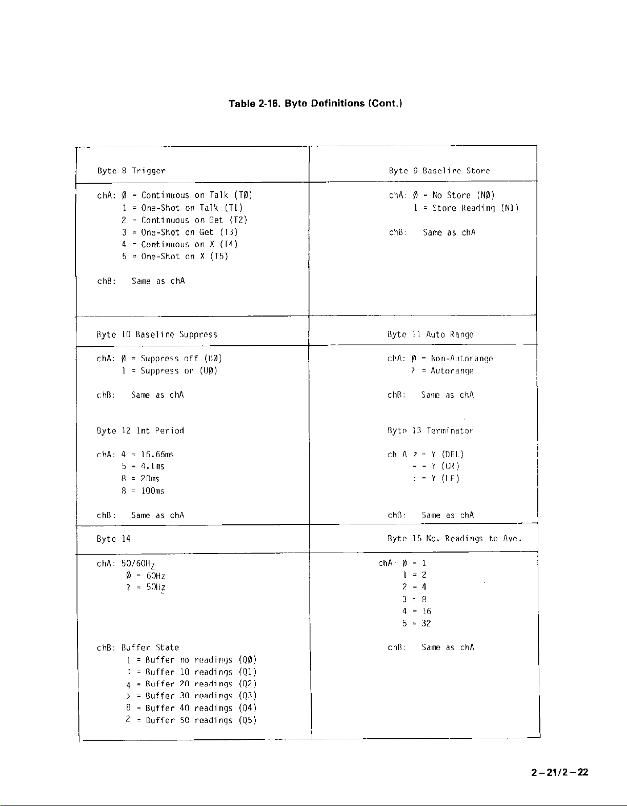
i
Byte 8
Triqger
I-
chA: 0 = Continuous on Talk (T0)
1 = One-Shot on Talk (Tl)
2
= Continuous an Get (TZ)
3 = One-Shot an Get (T3)
4
= Continuous on X (74)
5
= One-Shot on X (T5)
ch8: Same as chA
Byte
10
I
~~~
chA: 0 = Suppress off (UD)
Baseline Suppress
1 = suppress on (U0)
Table 2-16. Byte Definitions ICont.)
Dyte 9 Baseline Store
chA: 0 = No Store (N0)
chB: Same as chA
Byte
chA: 0 = Non-Autorangc
1 = Store Readinq (Nl)
11
Auto Ranqr
7 = nutoranqc
chl3 Same as chA
Byte 12 Int Period
chA: 4 = 16.66ms
5 = 4.1ms
8 = 20m
II = IflOms
chA: Same as chA chll: Same as chA
Byte 14
chA: 50/60HZ
0 = 60Hr
? = 5Ollr
chB: Ruffer State
1 = Ruffer no readings (00)
: = Buffer 10 readinqs (01)
4
= Ruffer 20 readings (42)
) = Buffer 30 readings (43)
8 = Buffer 40 readings (04)
2
= Buffer 50 readings (45)
chR:
Rytr 13 Terminator
ch A 7 = Y (OiL)
Eytc 15
chA: 0 = 1
chR: Same as chA
Sanr as chA
= = Y (CR)
: = Y (LF)
No. Readings to AVE,
I =2
2=4
3 = R
4 = 16
5 = 32
I
2-2112-22
Page 31

SECTION 3
ACCESSORIES
3.1 INTRODUCTION
Section 3 lists the optional modules and accessories
available for installation in, or use with, the Model 619
Electrometer/Multimeter.
3.2 MODEL 6191 GUARDED ADAPTER
The Model 6191 Adapter is an outboard option for use with
the Model 6194 Electrometer Module. It reduces effective
cable capacity by driving the inner shield of triaxial cable at
guard potential and thereby reduces time constants due to
high source resistances when measuring volts and ohms. By
reducing the additional effective cable capacitance to
approximately 2pF. it permits measurements from high impedance sources. (See Figure 3-1 .I
The Adapter OUTPUT connects directly to the Model 6194
Electrometer Module INPUT shielded connector. Guard
potential is obtained from the Model 6194 Analog Output.
The Adapter’s INPUT is connected to the measurement.
l-he unit is switch selectable for guarded or unguarded
operation. In the guarded mods of operation the outside
conductor of the input connector is at input common as opposed to power line ground for the “unguarded” mode.
Note that the Adapter will reduce the input common mode
voltage to a maximum of 30V RMS at DC to 60Hz. Also, a
10% isolation resistance can be placed in series with the
input by removal of an internal jumper. This is for use in
measurement of voltage sources which cannot tolerate the
Model 6194’s 500kOinput impedance in “zero check”
operation.
3.3 MODEL 6193 IEEE STANDARD 488 OUTPUT
The Model 6193 is an IEEE Standard 488 Bus Interface. It
permits the Model 619 to interface with any measurement
system utilizing the IEEE Standard Bus. The primary 5.bit
address is selected by five switches on the rear panel of the
Model 6193. This allows the selection of 31 primary listen or
talk address pairs. Binary 31 (11111) is reserved for the Untalk and Unlisten commands. The five rear panel switches
are set at the factory for a primary address of binary 6
(00110). The literature pertaining to the Model 6193
assumes that binary 6 is the primary address. (See Figure
3-2.)
Interface specifications (including line commands,
parameters and response time) are provided in the detailed
specifications which precede Section 1. Address modes or
Addressable (ADDR) or Talk Only are also switchable on the
rear panel of the Model 6193 module.
The Model 6193 was designed to be an interrupt driven I/O
device, The board uses the Motorola 68488 IEEE chip which
is capable of performing all IEEE Talker/Listener protocols.
Along with the 68488 IEEE chip, it also contains Motorola
3448A IEEE bus transceivers, which are capable of driving
and/or terminating the IEEE bus lines per the IEEE specifications. See Model 7008 IEEE-488 Digital Cable (paragraph
3.71 for cable interconnect.
Figure 3-l. Model 6191 Guarded Adapter
Figure 3-2. Model 6193 IEEE Standard 488 Output
3-1
Page 32

3.4 Model 6194 Electrometer Module
The Model 6194 is an Electromete Module that has three
functions -Volts, Ohms and Amps. It is an input module for
the Model 619 Electrometer/Multimeter. Addition of a se-
cond Model 6194 provides dual channel capability with indpendent ranges and functions as well as ratio and difference
capabilities. (See Figure 3-3.)
The Module structure consists of two printed circuit boards
mounted on a common rear panel. The inputs and analog
output of the Modal 6194 are located on its rear panel. The
oower and control inputs are obtained through the Model
PC edge connectors plugged into the Model 619.
All Model 6194 Electrometer Module functions and ranges
are programmed over the analog bus. Converted into its
various measurement configurations, the Model 6194 Electrometer Module processes an input measurement to a
200mV or 2V signal which is in turn processed further by the
AID Converter module and the Filter/Mu% module.
adjustment openings that are marked to facilitate making
the calibration alignments. (See Figure 3-4). The extender
cards allow easy access to the individual boarding for
troubleshooting purposes.
Figure 3-3. Model 6194 Electrometer Module
3.6 MODEL 6195 MAINTENANCE KIT
The Model 6195 is a maintenance kit for the Model 619.
The calibration cover is installed in place of the normal
Model 619 top cover during calibration. It allows the Model
619 to reach normat internal operating temperature and has
1
Figure 3-4. Model 6196 Maintenance Kit
3-2
Page 33

3.6 MODEL 6199 RACK MOUNTING KIT WITH
CHASSIS SLIDES
The Model 6199 is a rack mounting kit for the Model 619. It
provides the necessary hardware to mount the Model 619 in
a 5% inch (140 millimeter) rack height. The chassis slide
permits the unit to be pulled forward, the top cover remov-
ed, and internal adjustments or changes in configuration to
be made. (See Figure 3-5.)
3.7 MODEL 7006 IEEE-466 DIGITAL CABLE
The Model 7008 is a six foot (two meter) IEEE-488 digital
cable. The cable has 24 stranded wire conductors and is terminated with IEEE Standard 488 connectors. This will connect the Model 6193 to any IEEE Standard 488 connectors.
3.6 MODEL 6011 TRIAX INPUT CABLE
The Model 6011 is a four foot (1% meter1 low noise triax
cable terminated with alligator clips at one end and a triax
connector at the other end. This is a supplied accessory
with the Model 6194 Electrometer Module. (See Figure3-6.1
Figure 3-5. Model 6199 Rack Mounting Kit with
Chassis Slides
Figure 3-6. Model 6011 Triax Input Cable
3-313-4
Page 34

SECTION 4
PERFORMANCE VERIFICATION
4.1 INTRODUCTION
Performance verification is recommended upon receipt of
the instrument, to ensure that no damage or misadjustment
has occurred during transit. Verification may also be performed whenever the instrument’s accuracy is questioned
or following calibration.
NOTE
For instruments that are still under warranty
(less than 12 months since date of
shipment), and whose performance falls
outside specifications at any point, contact
your Keithley representative or the factory
immediately.
4.1.1 Required Test Equipment
The accuracy of the test equipment should be at least five
times better than the instrument specifications. The
minimum required accuracy ratings of the voltage, current,
and resistance sources are as follows:
I. Voltage sources:
A. 190mV to 1.9V .002%
B. 19v to 19ov .003%
2. current so”rces:
A. 1.9nA to 19nA .07%
B. 190nA to 1.9A .03%
3. Resistance sources:
A. 1.9kQ to 19kn .04%
B. 190kn to 1.9Mh2 .03%
C. 19Mn. 190MQ, 1.9G0 .07%
D. 19Gn - .2%
E.‘l90GO .8%
F. 1.5Tfl 2%
If the accuracy of the test equipment is not at least five
times better than the instrument specifications, additional
allowance must be made in the readings obtained.
4.1.2 Environmental Conditions
All measurements should be made at an ambient tempera-
ture within the range of 18’ to 28°C (65” to 82’FI and a
relative humidity of less than 70%.
4.2 MODEL 619 PERFORMANCE VERIFICATION
Use the following procedures to verify the basic accuracy of
the Model 619. If the instrument is out of specification at
any point, a complete calibration may be performed as
described in Section 6. However, if the instrument is still
under warranty, contact your Keithley representative or the
factory immediately.
NOTE
Performance verification should be performed by qualified personnel using accurate test
equipment with current calibration and
traceability.
4.2.1 Initial Conditions
Before beginning the verification procedure the instrument
must meet the following conditions:
1. If the instrument has been subjected to extremes of
temperature, allow sufficient time for internal
temperature to reach normal operating environmental
conditions specified in paragraph 4.1.3. Typically, it
takes one hour to stabilize a unit that is 10°C (18’FI out
of the specified temperature range.
2. Turn on the Model 619 and allow it to warm up for one
hour.
WARNING
Some procedures require the use of
high voltage. Take care to prevent contact with high potential circuits which
could cause electrical shock resulting in
injury or death.
4.2.2 Voltage Verification
Place the instrument in Zero Check, Channel A, Volts,
1.
and Manual ranging.
Set the Model 619 to the 200mV range and apply
2.
+ 190,OOmV to the Channel A input. Zero correct the in-
strument and verify a display reading of 0.00 - 3 to
within f 1 count.
Release the Zero Check and verify a display reading of
3.
+ 190.00 -3 to within *6 counts.
Repeat steps 1 through 3 using negative voltage.
4.
Refer to Table 4-1 and repeat the above procedures for
5.
the remaining voltage ranges.
If an Electrometer is installed in Channel B, repeat steps
6.
1 through 5 for that channel.
4.2.3 Current Verification
1. Place the instrument in Zero Check, Channel A, Amps,
and Manual ranging.
4-l
Page 35

2. Set the Model 619 to the 2nA range and apply 1.9000nA
to the Channel A input. Zero correct the display if
necessary.
3. Release the Zero Check and verify a display reading of
1.9000 -9 within f 59 counts.
4. Refer to Table 4-2 and repeat the above procedures for
the remaining current ranges.
5. If an Electrometer is also installed in Channel B, repeat
steps 1 through 4 for that channel.
7. For ohms sources greater than 200Mn the resistance
should be both guarded and shielded. The shield
prevents noise injection into the measurement and the
guard reduces response settling times (see Figure 4-2).
This can also be accomplished by using Model 8191
Guarded Adapter (see Figure 4-3).
Table 4-2. DC Current Performance Check
NOTE
For the 2OOpA through 20mA ranges, for
valid zero correction, input current must be
no greater than lOOpA. Zero correction does
not apply to the 2A range.
Table 4-I. DC Voltage Performance Check
Applied
Range
200mV
2v 1.9ooov
2ov 19.ooov 18.996 to 19.004 +o
200 19o.oov 189.98 to190.04 +o
*These display readings take into account the errors that
may be generated using the input sources listed in
paragraph 4.1.2.
4.2.4 Resistance Verification
1. Place the instrument in Zero Check, Channel A, Ohms,
and Manual ranging.
2. Set the Model 819 to 2kQ and apply 1.9000kQ to the input of Channel A. Zero Correct the display if necessary.
3. Release the Zero Check and verify a display reading of
1.9000 +3 within f 34 counts.
4. Refer to Table 4-3 and repeat the above procedures for
the remaining resistance ranges.
5. If an Electrometer is also installed in Channel B, repeat
steps 1 through 4 for that channel.
6. For ohms sources above 200kQ. the resistance element
should be shielded to prevent noise pickup, Refer to
Figure 4-l.
Voltage at lEO to 26OC
190.00mV
Allowable Readings
189.94 to 190.06
1.8997 to 1.9003 +o
*
-3
Applied
Current
1.9000nA
19.000nA
190.00nA
1.9000cA
19.OOO~A
19O.OO~A
1.9000mA
19.000mA
1.9000A
*These display readings take into account the possible errors that may generated using the input sources listed in
paragraph 4.1.2.
**When using the 2A range, the input must be applied to
the terminals designated as 2 AMPS MAX INPUT.
Table 4-3. Ohms Reference Check
Applied
Resistance
1.9000kQ
19.000kn
190.00kO
1.9000Mfl
19.000Mfl
190.00MQ
1.9000GO
19.000GO
190.00GO
1.5000TQ
*These display readings take into account the errors that
may be generated ,using the input sources listed in
paragraph 4.1.2.
!
Allowable Readinas
at 16O to 2PC
1.8966 to 1.9034
18.989 to 19.031
189.73
1.8976
18.943
189.46
1.8946
18.847
183.91
1.3800
to 190.27
to 1.9024
to 190.57
to 190.54
to 1.9054
to 1.9153
to 196.09
to 1.6200
-
l
+3
+3
+3
+6
+6
+6
+9
+9
+9
+ 1:
4-2
Page 36

r----
(shield)
--
1 Trim Cable
Figure 4-1. Resistance Source Shielding
r-------1
(shield)
Figure 4-2. Resistance Source Shiadling and Guarding
&?“dl _ _
r ,:lWi- --, 1
I ;
' I
' I
I 1
I i-----l,
L-- -----.
Resistance Source
I 1
,In A
Lly I]
I
' I
Pi" 1 Unity Gain Analog
Pin 2 Output
Trim Cable
y --f Electrometer *"put
1”
6191 Guarded +
Input Adapter +,
Ezl
Guarded
>
' Electrometer Analog Output
out
TO 6194
TO 6194
Figure 4-3. Measuring Resistance Sources Using Modal 6191
4-314-4
Page 37

SECTION 5
THEORY OF OPERATION
5.1 INTRODUCTION
This section contains functional and circuit descriptions Of
the component parts of the Model 619 and its related modules and options. The following components are included:
l Power Supply, PC-515
. Electrometer Module, PC-522 and PC-523
l IEEE-488 Interface, PC-517
. CPU, PC-518
l Display/Keyboard, PC-514
. A/D Converter, PC-520
. Filter/Multiplexer, PC-521
The Model 619 is a versatile Electrometer/Multimeter intended for use independently or with programmed test and
measurement systems. Current sensitivity and input impe-
dance meet or exceed practical limits for most applications.
Figure 5-l provides an overall operational view. Section 7
COmainS
schematic diagrams to aid in understanding circuit
operation.
5.2 POWER SUPPLY
The Power Supply, shown in Figure 5-2, is mounted on the
cabinet left side (as viewed from the front) and consists of a
PC board, Shield (30450). and Rear Panel (30448). The
Rear Panel contains the line fuse, line cord plug, and a series
ON/OFF switch (S303). Refer to Schematic Diagram 30516
and 32004 in Section 7.
AC power is provided to the Model 619 by the line
plug/filter, P301. Transformer 301 and the fan receive
power through the series circuit of fuse F301, and switches
S303 and S304. F301 and S303 are located on the rear
panel of the power supply. Switch 5304, mounted, on the
instrument front panel, is connected to the power supply
through R303. The AC power is also applied to the transformer, T301, through switches S301 and S302. These
switches permit transformer operation in four AC line
voltage ranges (refer to Table 5-l). The vent fan is powered
from the transformer primary through connector P302.
T301 acts as an autotransformer, setting the voltage level to
the fan.
Figure 5.1. Model 619 Block Diagram
6-l
Page 38

The transformer secondaries are grouped to provide power
to the Model 619 digital end analog buses. The digital portion, which provides +9.5V unregulated, consists of a
bridge rectifier CR301, filter capacitors C302 and C303,
bleeder resistor R302, and a parallel network consisting of
R301 and C301. The R301 and C301 network makes digital
common electrically equal to power line (chassis) ground.
The unregulated DC voltage developed is connected to the
mother board digital bus J304.
4
6194 Electrometer Modules, When two are installed, the
one on the left (as viewed from the rear) is Channel A. The
second Model 6194 is Channel 6. Figure 5-3 provides an
overall view of the Electrometer Module.
The heart of the design is a bootstrapped op-amp with an
ultra-low input bias current, The input overload protection is
provided by a ballast resistance and by current limiting on
the bootstrapped output. This circuit can be arranged in two
versions,
1. In Amps the circuit is arranged as a current to voltage
converter. Various feedback resistances are used to
measure a wide range of input currents.
2. The circuit can also be arranged as a high input impedance unity-gain buffer which is utilized for both volts
and ohms measurements. When in the Ohms configuration,
a constant current source consisting of a
bootstrapped voltage reference and various feedback
resistances is used to convert an unknown resistance to a
measurable voltage level.
The input to the module is via a triax connector. Separate
binding posts and a microphone connector are provided for
the 2 Amp current range and analog output respectively. All
input/output connections, along with a fuse, are located on
the rear panel of the module. A calibrated resistive divider
couples the module output to the input of an AID Converter
at 200mV and 2V.
Figut ‘e 6-2. Power S
;“PPlY
The analog portion consists of bridge rectifiers CR303 and
CR302, filter capacitors C304 through C312, voltage
regulators VR301 through VR303 and voltage bleeder
resistors R303 through R305. The AC power, 33VAC. that
is used by the Electrometer modules, is obtained from the
winding that powers the fl5VDC rectifier, filter, and
regulator portions of this circuitry. The regulated voltage
potentials, of +5VDC and fl5VDC are provided to the
mother board analog bus through connector J305.
6.3 MODEL 6194 ELECTROMETER MODULE
The Electrometer Module is a three-function component
(volts, ohms, and amps). The module construction consists
of two PCS’s mounted together with a common rear panel.
All of the module functions and ranges are programmed
over the analog bus. In its various measurement configurations, the module processes an input measurement to an
output of 200mV, or 2V, which is further processed by the
AID Converter and Filter/Multiplexer.
A Model 619 instrument may contain one or two Model
Power is supplied to the module via a transformer isolated,
floating power supply. The logic for decoding and latching
system commends to the Electrometer module are shown in
the block diagram in Figure 5-3.
5.3.1 Theory of Operation for the Model 6194 Electro-
meter Module
NOTE
When reading through the theory of operation for the Electrometer Module, refer to
Schematic Diagrams 305220 and 30523D.
located in Section 7.
The Power and Control inputs are obtained by plugging the
module P-C edge connectors into the appropriate connec-
tors on the Model 619 mother board (PC-516). This connec-
tor ties the module to the analog bus. Tables 5-5 and 5-6 are
the pin assignments for Channel A and S Electrometers
respectively. The input module identity is wired into the
mother board by transposing address lines A6 and Al be-
tween Channel A and Channel B locations on the mother
board.
5-2
Page 39

>
2
MIP Input
>
>
Analog Output
L
2 N4P Fuse
2 AMPS
Figure 5-3. Electrometer Module Block Diagram
PC-522 (305220) contains the module power supply, output circuitry and 1 Amp current range shunt. The power
supply portion of the circuitry provides three basic voltage
levels for the module. It provides f260VDC (TP-1 and TP-2
to input common) which is used by the output circuitry
when configured in the Volts or Ohms functions. It also pro-
vides f8VDC (TP-3 and TP-4 to TP-6) for use by the output
circuitry when configured in the Amps function. This also
eliminates the necessity of the *26OV supply having to sup-
ply greater than 2mA. The *17VDC ITP-7 and TP-8 to
TP-9) bootstrapped supply is used by the input amplifier and
ohms reference on 30523D. The transformer (T601) in addi-
tion to providing the various voltage levels, serves to isolate
the module from other instrument voltage sources.
The center of the output circuitry is a bipolar totem pole ar-
rangement consisting of high voltage transistors Q601,
Q603, Q604, and Q602. Resistors R601, R606, R608, and
R602 bias their respective transistors to ensure that the
voltage burden is equally divided between the two transistors at each end of the network. The network is current
notherboard Connections
biased by the voltage developed across CR615 through
CR618. CR615 through CR618 are essentially connected
across the totem pole arrangement. In the Amps function,
the contacts B and C of relay K602 short out R615 and
R617. This action increases the bias current level. The
bipolar networks consisting of 0605, Q606, CR620, CR619,
R613, and R615, limit the output current ranges. The top
ends of the high voltage “totem pole,” which are discon-
nected by contacts A and 8 of relay K601, prevent excessive power from getting to this particular portion of the
circuitry. In this mode, input is supplied to Q603 and Q604
through CR605 and CR608. Capacitor C605 serves as
response stabilization in the Amps configuration. CR605
through CR608 have an additional function in disconnecting
the f8VDC supply (TP-3 and TP-4 to TP-6) from the circuit
when it is in the Volts or Ohms functions. CR602 and CR604
disconnect the entire output circuit from the f260VDC
supply during input voltage overload in either volts or ohms.
The drive to the output circuit is provided by the bootstrap-
ped amplifier U651 on PC-523 and via Pin 56 on the intramodule bus.
5-3
Page 40

R607, R609, CR613, and CR614 provide extra drive current
to 0601 end Q602 when the circuit is operating near the
f 260V supply voltage levels. CR601 and CR603 protect the
emitter-base junctions of transistors 0601 and Q602 from
reverse voltage bias.
Controlling the configuration of the output circuitry arc :he
relays K601 and K602. These two relays are actuated by
R611, R610, Q607, end Q608 along with commutation
diodes CR623 end CR622. Control is provided via Pin 52 on
the intramodule bus from logic decoders on PC-523. K601
sets up the output for both Volts and Ohms functions providing for a on-inverting gain. K602 sets up the output for
the Amps function by providing for an inverting gain conversion.
The remaining circuitry on PC-522 includes the 2 Amp cur-
rent range shunt resistance, R605. The 2 Amp range has
separate binding post inputs, J601 and J602, and fuse pro-
tection F601. Relay K603 along with commutation diode
CR621 selects this range for connection to the module out-
put. Control is provided from logic decoders on PC-523 via
Pin 52 on the intremodule bus. Fuse F601 provides overload
protection end is mounted for access on the rear panel of
the module.
The rest of the Electrometer module circuitry is located on
PC-523. The circuitry includes the following:
*Input Amplifier
*Feedback Networks
*Ohms Reference
*Bootstrapped Power Supply Regulators
*Module Output Attenuator
*Control Logic Decoders.
The input amplifier consists of a group of components:
R664, R665, R668, R667, R669, R656, C651, C658, C661,
K656, and U651. The heart of this section of the circuit is
the Electrometer operational amplifier, U651. Providing the
active forward gain portion of the Electrometer module, this
circuitry is combined with the feedback networks and
bootstrapped ohms voltage reference to provide amps and
ohms along with the basic volts measurements.
Potentiometer R656 is used to trim the input offset voltage
for U651 while R667 and C661 provide a pole/zero stabilization to this forward gain block of the module. R669 is the
pull-up resistor for the output circuitry on PC-522. R668
provides the input protection for U651 by limiting the input
current. C658 (along with R668) provides input stabilization
on Volts and Ohms functions. Relay K656 is the zero check
contact with R665 limiting the zero check input current.
R664 and C651 provide compensation for this extra input
resistance in the Amps function.
Five feedback networks are used in setting up the Electrometer module for both the Amps and Ohms functions.
Utilizing the inverting mode of the module output circuitry a
current to voltage converter is obtained.
A bootstrapped voltage reference develops a constant current source for use with the non-inverting module output
circuitry mode, for ohms measurements. The five networks
used are 100 ohms fR601, R6071, 1Okohms fR659, R6521,
1Mohm fR660, R653). lOOMohms fR662, R6541, and
lOGohms fR663, R655, R666). Potentiometers R651
through R655 permit calibration of five networks. Capacitors C652, C653, C656, C655, and C657 stabilize the feedback response. Resistors R661 and R688 protect relay contact K657 form momentary current surges when capacitors
C653 and C656 are connected together. Connection of the
proper feedback network into the circuit is made by high
isolation impedance relays K651 through K654 end normal
isolation impedance relay K657. High isolation impedance
relay K655 provides a low resistance feedback network
which is used for amps zero check. Connection to the input
by relay K655 is made after R665, to limit the effect of the
realy contact resistance on the measured zero offset.
The ohms voltage reference consists of K658, K659,
VR653, U653, R676, R675, R672, R673, R670, R657, and
C662. The voltage reference is obtained from VR652; scaled
by R670, R672, and R673; and calibrated by R657. Op amp
U653 buffers the scaled voltage across R670 providing a low
output impedance to the feedback networks. C662 and
R675 serve to frequency compensate U653. R676 limits the
overload current on the output of U653. When VR653 is
switched in by relay K659, it limits the voltage across the
resistance being measured. The connection of the ohms reference to the feedback networks is made via relay K658.
Power to ohms reference and the input amplifier is provided
by the power supply circuitry which consists of U652,
VR651, VR652, R674, R677, R671, C654, C659, and C660.
These bipolar voltage supplies are bootstrapped to the Electrometer module output in the volts end ohms configurations. The negative voltage I-VRI is provided by regulator
VR651. Positive voltage f +VR) is provided by U652 which
amplifies the reference zener (VI76521 voltage. Capacitors
C654, C659, and C666 provide the transient response protection.
The parallel combination of R687 and C665 serves to limit
output current from U651 preventing excessive current
draw from U652 and subsequent latch up of the input circuitry.
The module output attenuator provides a 2 Volt full scale
output to the AID Converter for those ranges and functions
which result in a 20V or 200V full scale analog output, This
portion of the circuitry consists of R679 through R683 end
relays K660 through K662. As mentioned previously, the
A/D Converter has two ranges of operation, 2V and 200mV
full scale. Potentiometers R679 and R680 calibrate the two
attenuation gains of 0.1 and 0.01. Relays K660 through
K662 select either the unscaled module output fK661) or the
output attenuator fK662) x 0.01 or x 0.1 fK660).
5-4
Page 41

Resistors R686 and R678 are included to protect the Elec-
trometer module circuitry. Resistor R678 protects the
module from imposing a voltage potential from analog out-
put fJ652) common to module input fJ651) common.
Resistor R686 protects the module from transient voltage
input from the module output connection in the analog bus.
The remaining portion of the Model 6194 Electrometer cir-
cuitry is the Control Logic Decoder. This portion of the
module consists of U654 through U658, Q651, R685, C664,
end commutation diodes CR652 through CR663 and
CR664. U654 and U655 are octal D-type transparent latches
which store the appropriate data from control data inputs
end drive the module configuration relays. Data is clocked in
by decoding the module address through U656A and B.
Controlling the module requires “Function Byte” tU654l
and a “Range Byte” fU6551 which are latched with the appropriate address. These addresses and function/range
bytes are listed in Table 5-7. The identification or control
performed by each data bit in the function/range bytes is
listed in Table 5-8.
An acknowledge circuit, which consists of U656. R684, end
Q651, provides output to a wired NOR control line on the
“Analog Bus.” This serves to acknowledge the receipt of a
proper address by the module.
The section of circuitry consisting of U657C end D, R685,
CR664, and C664 performs a power up disable function.
The output of both latches U654 and U655 will be disabled
upon power up until receipt of a proper module functionbyte address. This prevents a random (and erroneous) configuration of the Electrometer module by power up transients. Additional logic prevents erroneous, simultaneous
actuation of relays which could result in damage to the
module.
Capacitors C666 through C668 prevent noise pickup and
subsequent erroneous relay actuatiOn.
5.4 MODEL 6193 IEEE-488 INTERFACE BOARD
The IEEE-488 Interface Board utilizes the Motorola 68488
IEEE IC which is capable of performing all IEEE
Talker/Listener protocols. The board was designed to be an
interrupt driven I/O device. The board contains Motorola
3448A IEEE bus transceivers, which are capable of driving
and terminating the IEEE bus lines per the IEEE-488
specifications.
A rear-panel accessible address switch is on the board for
choosing an IEEE Talk/Listener pair address for the Model
619. The IEEE connector is on the rear panel. An Interface
Bus Cable (Model 7008). six feet (2.meters) in length, is provided with the Model 6193 module. The five-bit Interface
address is beck-panel selectable. The address switches are
preset, prior to shipment, to primary address of binary 6
fOOllO).
5.4.1 IEEE Interface Board Theory of Operation
NOTE
When reading the theory of operation for the
IEEE Interface Board, refer to associated
block diaarems end Schematic Diaaram
30518 for deference designations. -
The Model 6193 IEEE Interface is built around the Motorola
68488 IEEE LSI device U706. The 68488 is a Motorola 6800
family peripheral IC.
The PCB is buffered on data, address, and control lines to
present only a 1 bus load. U703 buffers all of the address
and control lines. BAB-BA2 make up the RSB-RS2 register
selects on the 68488. The 68488 has 16 registers of which 8
are read only and 8 are write only. The use of the R/W
(read/write) line allows access to the two 8 register banks.
See Table 5-l for Register Commands.
U707A end U708A decode All, A12, and IOEN to form
BDSEL (Board Select) tTP1). The BDSEL decoding will
place the PCB at memory space address 9608,-97FF This
allows 2k of address space for the 68488 of which tie first
16 bytes are used. U7078 inverts BDSEL to form BDSEL.
U708B decodes BDSEL, E, end R/W to DRVENB (Drive
Enable1 fTP2) which when high allows the inverting tri-state
data buffers U711 and U710 to drive the data bus.
U707C inms the R/W signal to form R/W. U708C
decodes R/W, BDSEL, and E to form REC ENB (Receive
Enable) fTP3) which when low allows the inverting tri-state
data buffers U711 and U710 to receive from the data bus.
The E signal (System + 2) is used in the decoding of U708B
and U708C to turn the buffers OFF when they are not driving/sending, therby lowering their power consumption.
In the 68488 one of the 16 registers R4R is not present on
board the cmtself. When the chip decodes this register, it
generates ASE which is used to enable an external register
U709 onto the data bus. U709 is a tri-state buffer which is
tri-stated when ASE is high and drives the data lines when
-
ASE is low. The information on U709’s input is provided by
address switch S701, 5701 is located on the rear panel of
the Model 6193 IEEE-488 Interface Board. The necessary
pull up resistors for the switch bank are provided by the
thick film resistor network R701. The processor reads these
switches and then knows which Talker and Listener address
to assign to the 68488 chip, end thereby access the
instrument.
U702 end U705 are the data bus buffers for the IEEE bus.
U704 end U701 are the handshake and control buffers for
the IEEE bus. The buffers consist of four independent
driver/receiver pairs with bus termination resistors on
board. They also have the capability of either tri-state or
5-5
Page 42

Table 5-I. Register Commands
RS2
-
0
0
0
0
0
0
0
0
1
1
1
1
iEi
-
0
0
0
0
1
1
1
1
0
0
0
0
RSO
-
R/W
__
0
0
1
1
0
0
1
1
0
0
1
1
REGISTER TITLE
1
Interrupt status
0
Interrupt Mask
1
Command Status
0
NOT USED
1
Address Status
0
Address Mode
1
Auxiliary Command
0
Auxiliary Command
Address Switch
1
0
Address
1
Serial Poll
Serial Poll
0
SYMBOI
ROR
ROW
RIR
_..
R2R
R2W
R3R
R3W
R4R
R4W
R5R
R5W
1
1
1
1
-
1
1
1
1
-
0
0
1
1
-
1
Command Pass-Through
0
Parallel Poll
1
Data In
0
-
Data Out
R6R
R6W
R7R
R7W
5-6
Page 43

open collector operation depending on the bus requirement.
The Model 6193 is designed to use them in the open collec-
tor configuration. U707E. T/R2, and T/R1 form the control
for the bus buffers U701, U704, U705, and U702.
U702 and U705 data bus buffers are fully bi-directional as
indicated by the arrows on the schematic (305181. U701
Pins 3, 5, and 13 (which are NRFD, NDAC, and DAV
respectively) are also fully bi-directional. U704 Pin 11 lEOI)
is fully bi-directional. U707 Pin 11 (ATNI and U704 Pins 3
and 13 lREN and IFC respectively) are receive only and
U704 Pin 5 (SRQ) is send only. A typical section is shown in
Figure 5-4.
VR701 supplies the + 5 volt * 5% regulated power needed
by the PCB.
scratch-pad memory on board. With the 6840 LSI chip, the
CPU can have three hardware interval timers. It can support
both interrupt and DMA driven I/O systems. A 4MHz crystal
oscillator is used to provide all timing for the 6808 CPU chip
and digital system components. A partially decoded I/O
enable line (IOENI is provided for use by system I/O com-
ponents to ease their memory space decoding. The board is
capable of supporting signature analysis troubleshooting
techniques.
5.5.1 CPU Theory of Operation
NOTE
When reading through the theory of operation for the CPU board, refer to Schematic
Diagram 30519 for reference designations.
5.5 CPU BOARD
The CPU board has a circuit which resets the processor
upon power up to ensure proper system operation. This circuit can also be controlled via the watchdog line from one of
the interval timers in case of program malfunction. This
function will be discussed in more detail later in this section.
The CPU has provisions for 8K words of ROM (or EPROM)
program memory on board with decoding for an additional
8K ROM external. It also has provisions for up to 2K RAM
Pull
Up Enable
The Model 619 ElectrometerIMultimeter control processor
unit (CPU1 is constructed around the Motorola 8808 microprocessor (U905). This particular processor is a Motorola
6800 series processor with an internal clock.
The Motorola 6808 LSI microprocessor requires a 20msec
reset pulse when power is turned on to get its dynamic buffers and the clock running properly. This reset delay is provided by timer U917. The output of U917 is inverted by
U916D and applied to the reset pin of the microprocessor
SW Send/Rex
PA. Enable
S/R L
Figure 5-4. Data Bus Buffer
I
Dir. Comn.
5-7
Page 44

(Pin 401. It also goes to all other devices in the system which
require power up resets via bus Pin 28 (i.e., PIA’s, VIA’s,
etc.)
U913 is a Motorola 6840 timer peripheral. It is part of the
Motorola 6800 series family of parts. The 6840 KJ913)
contains three fully programmable hardware timers with interrupt and output capability. U916c is controlled by the
6840 (U913) software controllable timer 1, which monitors
the running software. U913 timer 3 is used to establish real
time interrupts to the running software. U913 timer 2 outputs a 120Hz signal on Pin 3 ITPIZJ to allow oscilloscope
monitoring for determining whether the IC is functional.
U913 is an I/O device to the system, U902B decodes BA9,
BAlO, BAll, and BA12 to form one chip select for U913.
The other chip select for U913 is provided by BIOEN which
will be discussed later in this section. The memory space is
SE@+SFFF,, of which eight locations are used by the
chip. Placing U913 in the I/O configuration gives it added
flexibility in that it can be used by DMA (Direct Memory Access) devices or other I/O components if needed. See Table
5-2 for Register Commands.
The 6808 microprocessor data bus D&D7 is buffered and inverted by U921 and U918 to form BDP)-BD7 and is provided
to the system. The unbuffered data bus is routed to all the
memory devices on the PC board. The control for data
transfer into the CPU is derived by 49038 (TP7). It decodes
+2, A15, A13, and R/W to form the RECENB (Receive
Enable) signal. The RECENB signal allows the buffer to
receive from the data bus. The control for data transfer into
the CPU is derived by U804C (TP61. It decodes R/W, BA,
E&I2 to form the DRVENB (Drive Enable) signal. The
DRVENB signal allows the buffer to drive the data bus.
Decoded +2 is used for all of the buffers in order to make
them G-state for reduction in power consumption.
The 6808 address bus A$A15 is buffered by U908 and
U901 to form BAQ -BA15 which is provided to the system.
To aid I/O device decoding in the system BA13, BA14,
BA15, and BVUA are decoded by U909C. 8, A, and U902A
to form the IOEN II/O Enable) signal. This signal is buffered
by U911 to form BIOEN. In addition to IOEN, U911 does all
RS2 RSI RSO
0 0 0
0 0 0
1
0 0
0 0
0 1 0
0 1 0
0 1 1
0 1 1
1 0 0
1 0 0
1 0 1 1 0 1
1 1 1 0 1 0
1 1 1 1
1
1 1
Table 5-2. Register Commands
I
R/W6= 0
CR2=0 Write #3
CR1 = 1 Write #3
Write Control
Register #I
Write MSB
Register
Write Timer #I
Latch
Write MSB
Register
Write Timer #2 Write
Latch
Write MSB
Register
Writer Timer #3
Latch
I
I
R/W=1
NOP
NOP
Read Status
Register
Read Timer #I
counter
Read LSB
Register
Read Timer #2
counter
Read LSB
Register
Read Timer #3
counter
Read LSB
Read LSB
Register
I
5-8
Page 45

the control line buffering; it buffers I, R/W, VMA (to form
BVUA) and BBA/DMAGNT (Direct Memory Access Grant)
for use by the Model 619 System.
All on board ROM memory decoding is done by U914A.
U903A, U904A, U912, and U91OB. U903A and U904Aform
the ROME (ROM Enable) signal. This enables U914A, the 2
or 4 decoder to select the appropriate daivce based on Al 1
(Pin 21 and Al2 (Pin 3) of U914. The 6808 requires vectors
from memory to branch to various sections of software.
These vectors must appear in locations FFFB,.FFFF, in the
memory space.
The Vector JAM signal allows the top block of ROM tc be
double address for this purpose. The top block responds to
FFF8 -FFFF, as well as its normal address. U912D and
d perform the necessary “0R”ing function. Therefore,
DSEL4 (TP4) decodes memory spaces B8@,-BFFF and
E@@@,-FFFF,. Signal DSELl ITP3) decodes A8&,-F,
memory space, ROM U924. Signal DSEL2 (TP21 decodes
ABgB,-AFFF, memory space, ROM U915. Signal DSEW
(TPl) decodes B&&B7FF, memory space, ROM U907.
The above process is used for 2716 memorY~s. Refer
to Table 5-3 for selection of PROMS. DSEW selects
A@@,-AFFF, memory space, ROM U907, and DSEL4
selects B@0&-BFFF, memcry space, ROM U906, as there
is only 8K maximum of ROM allowed. Memory space
C@@@,-DFFF, is reserved for external ROM. See Figure 5-5
for memory space map.
NOTE
The subscript H, as in EQ@Q,, denotes a
hexadecimal location in memory or hex
notation of a number.
All of the on board RAM decoding is done by U904B and
U914B. U904B decodes A14, A15, and+2 to form RAME
(RAM Enable) which enables U914B the 2 of 4 decoder.
When Aaislow, depending on the state of A10 (Pin 141,
either SRAwlect lower 1K) memory space &ij@$,-
@FF,,
or SRAM2 (Selected upper 1Kj memory space
04&07FF, is generated to select the appropriate RAM
bank. The RAM chips are 1K by 4K 121147) memory
devices; thus two chips in each bank are necessary for the
required 8 bits of data. U919 and U920 are the low order 4
bits and U922 and U923 are the hi&order 4 bits. The other
signal needed by the RAM’s is the WE (Write Enable) signal.
This signal is generated by U91OC and U909F which decode
R/W,42, and VMA.
The 5VDC regulated to lt5% is provided by VR901 and
associated capacitors. Crystal Y901 and capacitors C910
and C911 form the 4MHz oscillator clock needed by the
6808 IC. The 6808 divides this frequency by 4 and provides
a 1MHz output (Pin 37) E clock for system synchronization.
5.6 ISOLATOR BOARD
The Isolator board interfaces digital bus A to analog bus B.
Four optical isolators are utilized for signal coupling without
impedance coupling. Data, control, and address information is transmitted (with odd parity) to the analog side of the
isolator, using three of the optical isolators. At the same
time data from the A/D is transmitted to the digital side of
the Isolator board acrcss the fourth optical isolator.
The Isolator board also provides address decoding and
power for the display board as well as buffering for all lines
going to the display board from the digital bus.
Table 5-3. Jumpers for PROM Selection
Configuration
2716
PROMS (2kJ 0 X X 0 l X X X
W901 W902 W903 W904 w905 W906 W967 W908 W909
2732 PROMS (4k) l X X * 0 X X X 0
X = Don’t Care
*=hl
O=Out
5-9
Page 46

RAM 2k
I
BUFFER AREA lk
OPEN
ISOLATOR
FRONT PANEL PIAI 2643
FRONT PANEL PIA 256
CANNOT USE
l/O 256
266
8%fk?H
. 8400~
IEEE l/O 2k
OPEN
TIMER l/O 512
INTERNAL PROM 6k
EXTERNAL PROM 8k
Figure 5-5. Memory Map
%@H
A%%$
5-10
Page 47

5.6.1 Isolator Board Theory of Operation
NOTE
When reading through the theory of cperaticn for the Isolator Board, refer to
Schematic Diagram 30520D.
The Model 619 Isolator board is designed around the
Synertak 6522 Versatile Interface Adapter (U807).
The board is buffered on data, control, and address lines to
present one bus load to the Model 619 bus. U805 and U806
buffer the data lines. U803 buffers the control and address
lines. U801E. F, and U804A decode BA12, BAll, and
BIOEN respectively to form BDSEL (Board Selectl signal.
There is no buffering on lines BA12, BAll, and BIOEN as
well as BA8, BA9, and BAlO since they only represent one
load to the bus. U8OlA inverts BDSEL to form BDSEL.
There is also one chip select for U807. BDSEL is also inverted by U801B to form one chip select for the display
board PIA’s.
U802A decodes BA8, BA9, and BAlO to form other chip
selects for the interface. U802A Pin 4 selects U807. This
decoding arrangement places U607 in memory space
80@-8@1FF allowing 256 memory locations, however, only
16 are used. U802A Pin 5 forms Sl which selects U204 on
the display board. This arrangement provides 256 memcty
locations of which only four are used.
U802A Pin 6 forms S2, which selects U207 on the display
board. This provides 256 memory locations of which only
four are used. U802A Pin 7 is not used. All of the additional
signal control lines needed by the display board, E, A6, A7,
and R/W, are buffered by U803. The Data lines D&D7 are
buffered by U805 and U806. Reset and +5VDC and ground
(B corn) are not buffered. All of these lines go to the display
board through connector 801.
U804C and U8OlC decode R/W, E, and BDSEL to form
DRVENB (Drive Enable) (TPll in order to gate the data buf-
fers and to sand data to the data bus.
U801D and U804B decode R/W, E, and BDSEL to form
RECENB IReceive Enable) ITP2) in order to gate the data
buffers for receiving from the data bus.
The heart of the Isolator board is the Synertek 6522
Versatile Interface Adapter (VIA) a fully programmable I/O
device. The VIA internally consists of 2 software prcgram-
mable timers, 2 programmable bi-directional 8-bit parallel
I/O ports (similar to PIA’sJ and a serial communication port.
The device contains control registers which are prcgram-
mable in determining which of the many modes of operation
are to be utilized. Lines CBl and CB2 form the serial ccm-
municaticns port and PA@PA7 (Port A) and PB@PB7 (Port
BJ form the bi-directional parallel I/O ports. Internal register
bits are shown below in Table 5-4.
Table 5-4. Register Commands
RS3 RS2
0 0 0
RSl RSP) Register
0 @RB, IRB
0 0 0 1 @RA, IRA
0 0 1 0 DDRB
0 0 1 1 DDRA
0 1 0 0 Tl
0 1 0 1 Tl
0 1 1 0 Tl
0
1
:, A 1 Tl
0 T2
1 0 0 1 T2
1 0 1’OSR
1 0 1 1 ACR
1 1 0 0 PCR
1 1 0 1 IFR
1 1
1 1
0 IEB
1 @RA
Comments
Effect Handshake
Effect Handshake
Data Direction B
Data Direction A
Timer 1
Timer 1
Timer 1
Timer 1
Timer 2
Timer 2
Serial Port Data
Control Register
Peripherial Control
IRQ Mask
IRQ Enable
No-Efect Handshake
5-11
Page 48

For the serial I/O, the clock is programmed for a 500kHz
shift rate. The parallel I/O Port A lines PA&PA7 are programmed as inputs and Port B lines PB3-PB7 are also programmed as inputs. Port B lines and PB@ are programmed
as outputs.
Jumper J2 allows for odd parity checking, or no parity
checking depending on the system needs.
The regulated 5V f 5% is provided to the isolator digital
side by VR801 and associated capacitors.
The actual operation is as follows: A byte of data is written
via the software into the 6522 (VIA) serial out register. The
LSI device forms the clock and data for the serial bit streams
on CBl and CB2. The clock bit stream goes through U809A
and opto isolator AT3 and U810A to be the shift clock for
U812, U815 serial to parallel converters, and U816 parallel to
serial converter on the isolated side. U809A Pin 14 is a clock
enable which is utilized to disable the clock if the need
arises. U809A also provides the drive needed by the opto
isolator AT3. The data bit stream goes through opto isolator
AT3 and U810A to be the data for shift register U812 and
U815. U809B provides the drive for the opto isolator AT2.
U811 and U814 are generator parity/checker devices.
When the shifting is completed and U811 Pin 5 goes low,
this indicates odd parity. During the shifting operation, this
line goes low many times depending on the state of the shift
registers. Therefore, U81OB Pin 9 is an enable line, so that
when the data has been sent, the software causes an enable
low after shift. On the analog/digital bus this is used as an
address latch enable signal to latch in the address of the
analog device to which data is being sent. The data to be
written is placed on the outputs of U815 and the address is
placed on the outputs of U812. The software then sends
PB2, which disables the address latch enable, making the
enable line go high. At the same time U810D Pin 4 (latch
line) goes low, this causes the ACK line path to be selected
and ACK (Acknowledge) will be sent back from the analog
side. If the receiving analog device has latched in its ad-
dress, it responds via the ACK line. This is inverted by
U813A and goes to opto isolator AT4 and then to U807,
CAI, and PB7. CA1 interrupts the system when the ACK
line becomes true. Polling can be done to sense a change on
PB7. U813C provides the drive needed by the opto isolator
AT4. There are 2 types of error checking in transit. A parity
check followed by and ACK handshake completion. Upon
error, retransmission of data can be requested via the
software.
To receive data from the analog side, U807 PB2 is set to
disable the ACK path and enable the data path via U813D
Pin 12. The data shifts out at clock CBI rate from U816 go-
ing through U813C, D, and opto isolator AT4 into serial
parallel converter U808. It is then presented to U807 Port A.
The software can then read the E-bit data. On receive U816
recirculates the data presented to it by the analog side.
Thus, multiple reads and compares may be done via soft-
ware to enable error checking for receive data. Upon error,
retransmission of data can be requested via the software.
For test purposes Jumper Jl is provided to allow the
isolator to recirculate data or talk to itself (provided U815
Pin 13 is not being interrupted by the analog bus).
5.7 DISPLAY/KEYBOARD
The display/keyboard has three main areas, the keyboard,
annunciators, and numeric displays. The keyboard area
consists of a four by six matrix for a total of 24 switch locations. Sixteen of these switches are used in the Model 819
to select range, function and channel. The annunciator
area consists of 23 LED’s, The Model 619 uses 21 annunciators to display the status of the instrument. The display
area consists of a signed 5%.digit mantissa and a signed
2-digit exponent.
All the display board hardware decoding is done on the
ISOLATOR PCB. The decoding places the PCB at memory
address 81@@,-82FF,. U204 is located at 81@,-81FF,and
U207 is located at 82@,-82FF,. The power for the display
board is also derived from the Isolator board. All signal and
power lines are delivered to the display PCB via the connector cable.
5.7.1 Display/Keyboard Theory of ODeration
NOTE
When reading through the theory of operation for the display/keyboard, it will be
helpful to refer to Schematic Diagram
30515.
The heart of the display board consists of U204 and U207
Motorola 6800 family peripheral interface adapter chips
(PIA’s which are fully software programmable.
The PIA’s internally consist of two programmable control
registers which determine which of many modes of opera-
tion are to be used. The PIA’s also contain two program-
mable data direction registers, which are also data I/O
registers if bit 2 in the corresponding control register is set to
1. Both control registers are initialized to 3C ,. This configures the PIA’s for non-interrupt operation stan-
dard mode.
Data direction is configured for U204 by Port A outputs and
Port B outputs, and for U207 by Port A inputs and Port B
outputs.
U204 I/O Port B is the common cathode control strobe used
to turn the display on. Each of the eight lines turns on one
bank of LED’s plus one display digit. U207 I/O Port B is the
segment select control to select appropriate segments of
the display digits U204 I/D Port A lines. PAD, PAI, and
PA2 are the LED select controls to select the appropriate
5-12
Page 49

LED in the LED bank. U204 I/O Port A line PA3 is used to
key the beeper on and off; U204 Port A lines PA4-PA7form
the column lines to the switch matrix and U207 Port A lines
form the row lines to the switch matrix. U204 Port A lines
PA4-PA7 are used to enable the appropriate switch column
for the software switch scan. U207 Port A is used to read
the scanned switch bank to determine which switch has
been depressed. Switch debounce, N key rollover, and
switch validation are all done in software.
lb is set to approximately the value of Vin max/Rin.
Then Vin = Vmax, I = 0
Vin = 0, I = lb
Vin = Vmax, I = 21b
The charge balancing consists of an integrator, a positive
current source with a current switch, and the negative
signal current.
U201, U203, and U205 are buffers to drive the displays,
LED’s, and switches.
5.8 AID BOARD
The A/D board consists of the basic hybrid charge balance
dual slope AID. There are no references or multiplexed inputs. The control of this board is from the CPU board
through the digital Isolator board.
The input voltage is converted into a current in the GAMP
(Transconductance Amplifier). When the output of the Integrator ramps up to the threshold of the “D” flip-flop, the
2mA current source is turned on until the output of the Integrator ramps down below the threshold of the “D” flipflop. The number of pulses produced is accumulated in the
Event Counter.
Upon completion of Signal Integrate, and based on the
length of time determined by the number loaded into the Integration Time Counter, the number in the Event Counter is
multiplexed into the processor. The Event Counter is cleared
and the Single Slope current source is switched on. The
time required to ramp to zero is measured by counting the
clock in the Event Counter. This number is also multiplexed
into the processor. From these two numbers the total
number of counts can be calculated.
5.8.1 AID Theory of Operation
NOTE
When reading through the theory of operation for the A/D board, refer to Schematic
Diagram 30521.
The Transconductance Amplifier (GAMP) performs two
functions:
1. Converts the input signal voltage to a current for the
integrator.
2. It provides an offset to make the A/D bipolar. That is a
plus and minus voltage for input to the AID.
The op amp reference is biased at approximately -2.6 volts
or minus full scale by VR501
as a negative reference, and by
resistors R501 (25k) and KR501 (39k). Resistor R501 l3.9k)
forms a current source due to the constant voltage across it.
It is equal to the voltage across R501 (39k) due to the feedback action of the op amp.
When U513 Pin 1 (Signal Integrate) goes low, lsig (Signal
Current) flows out of the summing junction and ramps up to
the threshold of the “D” flip-flop, therefore, the current Icb
(Charge Balancing Current) is turned on for one clock
period. Icb is slightly greater than lsig full scale.
The value of C502 which is the integrator capacitor prevents
the output of the integrator from ramping below ground or
above + 5 volts.
U513A enables charge balance pulses only during Signal Integrate. 0503 prevents current limiting in the output of
U507 op amp and clamps the output of the integrator to * 5
volts to protect the “D” flip-flop. U507 is a FET input op
amp that prevent any extra currents from flowing out of the
summing junction during the instantaneous overloads as the
charge balance pulses or signal current are switched OFF
and ON.
R503 is a linearity resistor. The nonlinearity in the A/D is a
square law curve. The amount of current removed from the
summing junction by this resistor is proportional to the
voltage across the diode junction to the summing junction in
U507. This induces a compensating logarithmic nonlinearity. The basic nonlinearity is only 10 to 50ppm. The compensation corrects this error to 1 to IOppm.
The residual charge on the capacitor is ramped down to zero
volts by the Start Single Slope control signal. The single
slope current is l/128 of the charge balance current. This
ratio is between R501 (320k) and R501 i2.44k) taking into
account the base emitter coltage drops of Q505, Q506, and
Q507d. However, the charge balance is on only 50% of the
time, so the effective ratio is 11256 (Refer to Event Counter
Operationl. During operation, the last digit displayed is ap-
proximately the single slope contribution, so this ratio only
has to be accurate to 1% to 10%.
The IMCI line has 10 volts on it and is a byproduct of the
reference circuit on the Filter/Mux board.
The Clock is composed of an oscillator and a divider circuit.
The oscillator is a classic Pierce oscillator circuit developing
4.915MHz. U516 (74193) divides the oscllator frequency to
307.2kHz and 614.4kHz. The 307.2kHz after being buffered
by U508A is divided down even further to 1200Hz by U505
(LS393). The 614.4kHz is gated into the charge balance circuit through U513C and 8.
5-13
Page 50

The AID essentially runs on its own until it has data for the
processor at certain essential times during the conversion.
The Event Counter is a 16 bit binary counter that is used in
two modes, The first mode is to count the number of charge
balance pulses during Signal Integrate. The second mode is
to count the 5MHz clocks during the ramp down of the
Single Slope. Using the 5MHz clock in this manner, makes
one Single Slope count equal to l/1024 of charge balance
counts. The resolution is thereby increased. The output of
this counter is multiplexed to the Data In Bus, and then to
the processor, 8 bits at a time.
NOTE
The ACK line is low under the conditions
described in the preceding steps 1 through
8.
5.9. FILTER/MULTIPLEXER BOARD
NOTE
When reading through the theory of operation for the FilterlMux board, refer to
Schematic Diagram 30524.
The Integration Time Counter consists of an 8 bit prescaler
counter U505 and an 8 bit programmable down counter
U509 and U510. U505 receives its input from the lowest frequency tap of the oscillator divider. U505 drives U510 and
therefore U509 with a frequency of 1200Hz. U509 and U510
are loaded from the processor. Thus, the integration time
can be programmed in increments of 833 microseconds.
This is convenient for integration periods of 16.66msec or
20msec.
The Control Bit Latch register, U517, holds the control bits,
to set up the various control and data paths on this board.
1, Bit 0’. LS bvte A turns on the Vi-state buffer, U512, onto
the Data In Bus.
2. Bit 1, MS byte A@ turns on the tri-state buffer, U519, onto the Data In Bus.
3. Bit 2, Single Slope Al starts slope and remains at logic
level 1 during the complete ramp down. The counting
and the ramping will stop automatically when the ramp
has crossed zero.
4. Bit 3, Parity. this is not used in hardware. It is used for the
parity bit in software.
5. Bit 4, Force Integration is normally a logic 1 for the present software, but is could be used to produce long integrations under direct processor control.
6. Bit 5, Event Counter ACK Enable normally a logic 1 in pre-
sent software. It is used to sense MS8 of Event Counter
qn the ACK line when an overflow occurs in a long integration.
7. Bit 6, integrate ACK Enable is normally a logic 1 in pre-
sent software. ACK is asserted during the time the integration time counter is counting.
8. Bit 7. Clear Al resets all counters to zero and thus stops
all functions in progress.
A 3 input Nand gate package (U504) is used to decode so
that only 3 of 8 bits are high at any time. There are two addresses on the board.
1. B$, latches the data on the control Bus into the Integration Time Counter. The address must be present for 4
microseconds and no longer than the integration time,
otherwise it will retrigger the integration.
2. A8, latches the data on the control bus into the Control
Bit Latch on the trailing edge of the address decoding.
The Filter/MUX board consists of the signal conditioning circuitry and references for the A/D board. Channel A and B
Electrometers are selected by the appropriate relays. These
relays (K401 and K402) connect signal and ground on the
Electrometer module to the Al D’s signal and ground inputs.
The Signal FET Driver amplifier (U405) is used to minimize
charge injection from the gate source capacitance of the
FET, into the filter when it is in use.
The Input Buffer (U404) is bootstrapped for linearity. It can
be switched from a times one gain to a times ten gain. Two
references are available for calibration; a 2 volt reference
and a 0.2 volt reference.
The Electrometer Multiplexing relays switch signal and
ground from the two Electrometer modules to the input of
the A/D. The switching is done by K401 and K402. The
relays also provide isolation between the two channels.
The Ground Relay K405 protects K401 and K402 from arcing or flashover when switched to the AID. A large transient is possible when this happens due to the stray
capacitance between the AID ground and the Electrometer
ground R431 (IOk) limiting the current during the transient.
K405 is then closed to eliminate rejection problems caused
by having the resistor in the ground lead.
The RC filter, which is a single pole filter, can be switched
into the input of the A/D Converter via relays K403 and
K404. The filter consists of C408 and C409, R433, R436,
and R437.
The neon bulbs DS401 and DS402 fire at approximately 85
volts in order to protect the capacitors in the filter from over
voltage. The leakage resistance at this point, due to the
neon bulbs, will be an order of magnitude less than the least
significant digit, i.e., approximately Ippm. This means the
off resistance of the neon bulbs is > = 130Gohms.
The short time constant RC (C410 and C411, R436, R437,
R433, and R434) is included to suppress high frequency
noise from the output of the Electrometer modules. When
K403 and K404 are actuated, R435 and R432 limit the
resulting discharge current.
5-14
Page 51

Protection for the input to the AID Buffer amplifier is provided by FET’s Q407 and Q412. They clamp the input to * 5
volts.
The op amp U405 provides a zero volt difference bias
voltage for the signal FET Q409 and compensating FET
Q406. Q406 provides cancellation of the charge injection
due to gate-drain capacitances of these FET’s into the filter
capacitors C408 and C409.
FET’s 0410. 0408. and 0411 provide inputs for Zero, 2
volts, and 0.2 volts respectively.
The A/D Buffer Amplifier is an Xl or X10 gain, high input
impedance, low output impedance stage to couple the
various inputs to the 5k input of the AID board. The different gains are obtained by switching in the different feed-
back resistors. The resistors are R418 and R419. Thev are
switched in and out by FET’s Q404 and Q405. The op’amp
has a bootstrapped power supply of *6 volts. The boot-
strap supply consists of U403, Q401 and C403, 13404, and
R407. The bootstrap ground potential is the potential at the
summing junction of U404. This ground is used to reference
the drive resistors of the other input FET’s 0408, 0410, and
Q411. Decoupling or compensation to prevent instability in
the bootstrap is provided by RC’s, C403/R404 and
C402/R405.
The control or logic section consists of two latches. One
I IIU V”llllUl “I ,uy,r. S~lil,“II Gu.l1151SL3 “I Lvw
latch to switch relays and one latch to contra, LIIr I L latch to switch relays and one latch to control the FET switches for the A/D buffer amplifier. U408, wk’ ‘~ . ches for the A/D buffer amplifier. U408, which is the FET
control latch, clocks in the data that is on the control latch, clocks in the data that is on the control bus on
the trailing edge of address @,,, The output of U408 drives
U406 and U407 which are open collector comparators.
These comparators are used to level shift the 0 to 3 volt TTL
signal to -15 to + 5 volt signal to drive the FET switches.
Assignments are signals to drive the FET switches. The bit
assignments are as follows:
1. Bit 0, Al put the buffer amplifier in X10 gain. Ag’puts it in
the Xl gain.
2. Bit 1, Al turns on the signal FET IQ409).
3. Bit 2, Al turns on the zero FET (Q410).
4. Bit 3, Al turns on the 2 volts FET W408).
5. Bit 4, Al turns on the 0.2 volts FET (Q411).
6. Bit 5, not used.
7. Bit 6. Al turns on the charge compensating FET
IQ406).
The software drives this bit with the compliment of Bit 1.
8. Bit 7 Parity. Not used in hardware.
U409. which is the relay latch, clocks in data that is on the
control bus on the trailing edge of address D$.
The bit assignments are as follows:
1. Bit 0, A0 turns on relay K401, Channel A.
2. Bit 1, A0 turns on relay K403, Channel A’s filter
capacitor.
3. Bit 2, A0 turns on relay K402, Channel B.
4. Bit 3, A0 turns on relay K404, Channel B’s filter
capacitor.
5. Bit 4, A0 turns on relay K405 ground relay.
6. Bit 5, not used.
7. Bit 6, not used.
8. Bit 7, Parity. Not used.
5-15
Page 52

Table 5-5. Analog Bus Connector Pin Assignments Valid for Channel A
SIGNAL
4 COM*
13VAC
h f?OM*
--...
3LANK
3LANK
3H A HI
3H A LO
4 COM*
4 COM
4 COM
4 COM
+ 15VDC
+ 5VDC
+ 5VDC
A COM”
A0
A3
A5
LATCH El
D0pl
442
\lABLE 37
DW
M3
A COM”
IM Ap,
IM A2
IM Ax (C
IM A6
IM A8
IM Al0 59
IM Al2
2-l A LO)
PIN
1
3
5
7
9
11
13
1;
19
21
23
25
27
29
31
33
35
39
41
43
45
47
49
51
53
55
57
61
PIN
2 A COM*
4 33VAC
6 A COM*
8
10
12
14
16
18
20
22
24
26
28
30
32
34
i”s
40
42
44
46
48
50
52
54
56
58
60
62
SIGNAL
BLANK
BLANK
CH A HI
CH A LC
A COM*
A COM
A COM
A COM
- 15VD(
+5VDC
+ 5VDC
Al
A2
A4
A6
A COM’
c01
D03
D’$5
D$7
/ACK
IM Al
IM A3
IM A5
IM A7
IM A9
IM All
IM Al3
5-16
*Shielding ground not to be used as a current supply line.
Page 53

Table 5-6. Analog Bus Connector Pin Assignments Valid for Channel B
A COM*
CH A HI
CH A LO
CH B HI
CH B LO
A COM’
A COM
A COM
A COM
+ 15VDC
+ 5VDC
+ 5VDC
A COM*
Al
A3
A5
LATCH ENABLE
000
D02
004
Do6
A COM”
IM B0
IM 82
IM 84 ICH A LO)
IM B6
IM BI3
IM 610
IM 812
1
3
5
7
9
11
13
15
17
19
21
2
27
29
31
2
37
39
41
43
45
47
49
51
53
55
57
59
61
PIN
2
i
8
10
12
14
16
18
20
22
24
26
28
30
32
34
36
38
40
42
44
46
48
50
52
54
56
58
60
62
SIGNAI
A COM’
33VAC
A COM’
CH A HI
CH A L(
CH B HI
CH B LC
A COM”
A COM
A COM
A COM
- 15VD(
+ 5VDC
+ 5VDC
A0
A2
A4
A6
A COM’
@‘I
D03
D05
D07
/ACK
IM Bl
IM 83
IM 85
IM B7
IM 69
IM 611
IM 813
*Shielding ground not to be used as a current supply line
5-17
Page 54

Table 5-7. Electrometer Control
ADDRESSES
CHANNEL A, FUNCTION BYTE
RANGE BYTE
CHANNEL B, FUNCTION
RANGE BYTE
VOLTS
VOLTS, ZERO CHECK
OHMS
lkohm to 1Okohm
lOOkohm to lOOMohm
1Gohm to 1OOOGohm
OHMS, ZERO CHECK
1 kohm to 1Okohm
lOOkoh, to lOOMohm
1Gohm to 1OOOGohm
AMPS
External Feedback
1nA to 1pA
IOpA to lOOpA
1 mA to lOmA.
External Feedback
1A
AMPS, ZERO CHECK
InA to 1pA
lOpA to 100&A
1mA to lOmA.
External Feedback
BYTE A/D RANGE
000 0101 (05)
000 1001 (091
000 0110 (06)
000 1010 (OAI
l*ll 0111 (FF, 871
1'11 0011 (FB, 83)
O"O1 0110 (5E. 16)
lx01 0110 (DE, 96)
lx11 0110 IEE, B61
O"O1 0010 (5A. 12)
lx01 0010 (DA, 921
lx11 0010 (EA. 82)
1"ll 0101 (FD. 65)
I*11 0101 (FD. 65)
Ox11 0101 (7D, 351
I"11 0101 (FD. 651
I"10 0101 (ED, A51
lx10 0101 (ED, A51
O*lO 0101 (6D. 251
l*lO 0101 (ED, A5)
5-18
RANGE BYTE
VOLTS
IOOmV
1v
1ov
1oov
OHMS
lkohm
1Okohm
lOOkohm
1Mohm
1OMohm
IOOMohm
OHMS
IGohm
lOGohm
1OOGohm
1OOOFohm
BYTE
1111 0111 (F7)
1111 0111 (F7)
1101 1101 (DD)
1111 1101 (FDI
1111 0011 IF31
1111 0011 (F3)
1111 0011 (F3)
1111 0011 (F31
11100111 (E7)
11100111 (E7)
1100 1101 (CD)
1011 0111 (87)
1001 1101 (9D)
1011 1101 (BD)
A/D RANGE
1oomv
IV
IV
1v
1OOmV
1v
1OOmV
1v
1OOmV
1v
1v
1v
1v
1v
Page 55

Table 5-7. Electrometer Control (Cont.)
\MPS
1nA
1OnA
lOOnA
llrA
10fiA
1OOA
1mA
1OmA
1A
External
Feedback
“Range Disabled Bit (DO61
1 Range Byte control disabled
0 Flange Byte control enabled
Byte data is binary.
Data in parenthesis is in
hexadecimal notation.
11100111 (E71 1OOmV
0111 (E71
1110
0011
1111
0011 (F3)
1111
1111 0011
1111 0011
0111
0111
0111 0111
1110 (FE)
1111
1111 0111
(F3l
(F31
(F3)
177)
(77)
IF71
IV
1OOmV
1v
1OOmV
1v
1OOmV
1v
IOOmA
IV
Table 5-9. Control Data Bit DesiQnatiOns
RANGE BYTE
K603 IAmp
k662 X0.1/X0.01 Output
K656 Volts/Ohms,
K652 lMohm/lOkohm Feedbacl
Zero Check
Not Used
K655 Amps, Zero Check
K659 ohms Input
K661 Xl output
K653 IOOMohm Feedback
K660 x0.1 output
Voltage Limit
Range Disable
K657 IOkohm Feedback
K654 IOGohm Feedback
K651 IOOohm Feedback
‘Relay Designation Refer to Schematics 305220 and 30523.
5-19/5-20
Page 56

SECTION 6
MAINTENANCE
6.1 INTRODUCTION
This section contains information necessary to maintain the
Model 619. Adjustment calibration, troubleshooting and
fuse replacement procedures are provided.
6.2 PRE-POWER UP PROGRAMMING
The top cover of the Modal 619 must be removed to check
or change the LINE VOLTAGE, LINE FREQUENCY and
BEEPER switches. To remove the top cover, remove the
two retaining screws located at the rear of the instrument
and lift the cover off.
WARNING
All service informrrtion is intended for
qualified electronic maintenance personnel only.
WARNING
To prevent a shock hazard, remove the
line cord and all test leads from the in-
strument before removing the top
cover.
Sat up switches 5301 and S302 par instructions given in
Table 6-l. instructions are also printed on the power supply shield.
Refer to Table 6-l and select and install the properly rated
line fuse.
CAUTION
Installing a higher rated fuse than the
one specified could result in damage to
the instrument.
Reinstall the power supply shield.
Select the appropriate line frequency by setting switch 4 of
S801 (Figure 6-l) to the closed position (0) for 60Hz opera-
tion or to the open position (1) for 50Hz operation. If the
Modal 619 is on while changing the switch position, the new
frequency setting will not be accepted until the instrument is
turned off and then powered back on.
6.3 BEEPER SELECTION
The beeper is programmed to be operational at the factory;
however, it can be disabled if so desired.
1. Remove the top cover.
6.2.1 Line Voltage and Frequency Selection
Position switches and install appropriate fuse
as
follows
(refer to Figure 5-21:
1, Remove the power supply shield by carefully lifting it off
of the four retaining clips.
Table 6-l. Line Voltage Selection
Line Voltage
9ov-1lOV
105V-125V
18OV-220v
21OV-250V
s301
HI-LO
Switch Switch
LO
HI 1lOV
LO
HI
S302
llo-220v
1lOV
220v 3AG. SLO BLO
220v
WARNING
To prevent a shock hazard, ramova the
line cord and all test leads from the instrument before removing the top
cover.
TYPO
3AG. SLO BLO
25OV. 1A
3AG. SLO BLO
25OV, 1A
25OV. 1/2A
3AG, SLO BLO
25OV. 1/2A
6-l
Page 57

2. Set switch 1 of S801 on the Isolator Board to the open
position (1) (refer to Figure 6-l).
3. Reinstall the top cover.
6.4 READING RATE SELECTION
When the Model 619 is in the Front Panel Mode and the 5%
digit resolution mode, two different reading rates can be
chosen via S5 (2.41 rdg/secl or S8 IO.30 rdglsec). See
Table 2-6. To select the S5 reading rate:
1, Remove the top cover.
WARNING
To prevent a shock hazard, remove the
line cord and all test leads from the in-
strument before removing the top
cover.
2. Set switch 2 (Figure 6-l) on the Isolator Board to the
closed position IO).
3. Reinstall the top cover.
To select the S8 reading rate:
1. Remove the top cover.
WARNING
To prevent a shock hazard, remove the
line cord and all test leads from the instrument before removing the top
cover.
2. Set switch 2 (Figure 6-l) on the Isolator Boardto the open
position (1).
3. Reinstall the top cover.
6.6 CALIBRATION INTRODUCTION
Perform the following procedures and make the
adjustments indicated to calibrate the Model 619 Electrometer/Multimeter, and the Model 6194 Electrometer
Module(s). Calibration of the Model 6194 requires installation in a Model 619 main frame. Therefore, the following
procedures include calibration of the module as part of the
entire instrument. Calibration should be performed yearly
(every 12 months) or whenever performance verification
(see Section 3) indicates that the instrument is out of
specification.
SWITCH 1 1 = BEEPER ON 0= BEEPER OFF
SWITCH 2 1 =S8 RATE AT 5Xd O=S5 RATE AT 5%d
SWITCH 3 EXTERNAL TRIGGER
SWITCH 4 1 =50HZ 0=6%
r
Figure 6-l. Isolator Board and Switches
OPEN = 1
CLOSED =0
6-2
Page 58

NOTE
Calibration of the Model 619 requires currents and impedances outside the ranges
normally encountered in calibration
laboratories, Due to the need for special
handling, high level technical expertise, and
non-standard test equipment, it is strongly
recommended that the Model 619 be return-
ed to the factory for service and/or
calibration.
6.6 CALIBRATION/TEST EQUIPMENT AND
CONDITIONS
6.6.1 Recommended Test Equipment and
Related Information
Test equipment for calibration is listed in Table 6-2. Alternate test equipment may be used. However, the accuracy of
the alternate test equipment must meet specifications listed
below:
Voltage Sources t *20ppmj
190.0000mV
1.999999v
19.99999v
199.9999v
Current Sources f *200ppml
19.000mA
190.00wA
1.9000pA
19.000nA
Calibration Resistance
19kD f IOOppm
19GO * 1OOOppm
6.7 INFORMATION AND ASSUMPTIONS
6.7.1, Standards
Maximum Allowable Input:
Input overload source must be noninductive with a
capacitive component less than 5OOOpF.
Isolation:
Input LO to power line ground, ) lOOMohm shunted by
approximately 75OpF. AID Converter common to
Electrometer Module Input, (0.5pF.
Input Stability:
Stable with < 5OOOpF input to input common and/or guard
(analog output in Volts or Ohms) and analog output to input
common.
Ranging:
Manual or Automatic in Talk-Only mode.
Manual in Addressable mode.
Range exponents are multiples of three (0, *3, +6, +9,
*12, *15, *la).
Weight:
Model 6194 Electrometer: lib. 1202. (0.81kgj
Model 6193 IEEE-488 Interface: 6.50~. (0.18kgj
Model 6191 Guarded Adapter: 502. (O.lBkgj
Maximum Allowable Common Model Slew-Rate:
109 volts/sac., with no loss of data or commands across
isolator.
Analog Output Characteristics:
Voltage: V,,, = V
Current: V,“r =
* 1 mV
[Is x RfeedbackjflmV=200mV F.S. on
2nA. 200nA. 20rA, 2mA ranges.
2 Volt F.S. on 20nA. 2pA. 200pA. 20mA ranges.
Resistance: V,,r
=R, x lsense* 1mV (Output same as
voltage across unknown. Refer to paragraph 6.6.1 for F.S.
values.1
Output Resistance: lkohm
Maximum Allowable Output Current: ImA
Maximum Allowable Input Voltage (externally applied with
respect to Analog Output common): 20 Volt peak.
6.8 VOLTS
Accuracy Specification Assume:
With input offset corrected by Zero Correct function after
warm-up, and every 24 hours thereafter. Correct whenever
IdT,I ) 1°C. Spec exclusive of noise. Specified temperatures
are package ambient. With ) 1 line period integration.
Temperature Coefficient Specifications Assume:
With source resistance ( lOOMohm.
NMRR Specifications Assume:
> 55dB valid with DC inputs up 90% of &full scale.
Rating based on 1 digit injection on 2 Volt through 200 Volt
ranges and 4 digits injection on 200mV range.
At 50 and 60Hz. max. rdg rate, with 1 line-period inte-
gration.
Filtering adds 25dB.
CMRR Specifications Assume:
) lOOdE valid for 200mV and 2 Volt ranges. Rating
decreases to 80dB for 20 Volt range and 60dB for 200 Volt
range.
At DC, 50, and 60Hz with lkohm unbalance, max. rdg rate,
1 line-period integration.
Analog Settling Time Specifications Assume:
Exclusive of input noise, with less than 1mA of total resistive
and dV/dT capacitive analog output load Imax. capacitance
5000pfl.
Exclusive of source response time and AID conversion
time. Refer to Model 619 Systems Use Specifications for
digitization times,
Input Noise: 2OpV p-p Assuming:
With source resistance < lOOMohm. Over 1 minute, unfiltered, self-generated.
6-3
Page 59

Table 6-2. Recommended Test Equipment
Item Description
A DC Calibration
Output
1.999999v
19.99999v
199.9999v
B Current Source
C Decade Resistor
1 OpA9A
120kD/lOk-Step S
llOMD/lM-Step S
D R-289-IOG
IOGO
Resistor
E R-289-100G
lOOGO
Resistor
F Ohms Calibration
6.9. AMPS
106-10’3
External Feedback has the following specifications:
ACCUrElCy
0.002% or 20ppm
0.01%
5Oppm
50wm
1OOOppm
1OOOppm
Mfr. Model
Fluke 343A 1
Valhalla 2500 1
ESI SR-1010 1
SR-1050 1
K-l
K-l
Guideline 9520 1
Input. NMRR, Noise, and Analog Settling Times will be a
function of the feedback element. Displayed reading is the
voltage across the External Feedback element.
2
1
TEMPERATURE
RANGE READING
MAXIMUM
External
Feedback 1.9999 Wts,
ACCURACY COEFFICIENT
f year. 230 *ST
* (%rdg + digits)
0.01% + Id
o-1wc
an* 28.5oQC
ff% rdg+digits~,T
0.cK32% + 0.3d
m,
External Feedback range requires user supplied feedback
element for current to voltage conversion (resistor), charge
to voltage conversion (capacitor), etc. Accuracy,
Temperature Coefficient specifications are in addition to
(but not including) that of feedback element. Feedback element is connected from the Analog Output to the Module
6-4
Accuracy Specifications Assume:
With input offset corrected by Zero Correct function after
warmup and every 24 hours thereafter. Correct whenever
dTa ) l°C. Spec exclusive of noise. Specified temperatures
are package ambient. With > 1 line-period integration.
NMRR Specifications Assume:
Valid with DC inputs uo to 90% of + full scale.
At 50 and 60Hz; max.’ rdg rate, with 1 line-period integration,
Filtering adds 25dB.
Analog Settling Time Specifications Assume:
With less than ImA of total resistive and dV/dT capacitive
analog output load (max. capacitance 5OOOpF).
Exclusive of source response time and A/D conversion
time.
Refer to Model 819 System Use Specifications for digitiza-
tion times.
Page 60

Input Noise:
2fiA : 5d
20pA: 0.5d
200fiA. 20r~A. 2fiA, 2A : 2d
2r1A. 200pA. 20fiA : 0.3d
External Feedback : 0.3d
6.13 CALIBRATION COVER INSTALLATION
Calibration should be performed using the Model 6195
Calibration Cover (see Figure 8-21. This cover permits access to Model 619 and to Model 6194 adjustments, while
allowing the instrument to reach normal internal operating
temperature. Install the cover as follows:
Digits, peak to peak, over 1 minute, unfiltered, selfgenerated, 4% digit readout.
Input Voltage Drop:
Whenever a series connected voltage source and resistor
are used to calibrate, or verify the Model 619 Amps range,
the effect of the input voltage drop must be taken into account. From the specifications the maximum value of 1mV
will constitute an uncertainty in the effective accuracy of the
voltage source. Maintaining this source at voltage levels
) 1.9V will reduce this uncertainty to : 0.05%.
8.10 OHMS
Accuracy Specifications Assume:
With input offset corrected by Zero Correct function after
warm-up and every 24 hours thereafter. Correct whenever
dT, ) l°C. Spec exclusive of noise. Specified temperatures
are package ambient.
With ) 1 line-period integrations.
~External voltage sources ( 5OpV.
6.11 ENVIRONMENTAL CONDITIONS
Calibration should be performed under laboratory condi-
tions having an ambient temperature of 23O * 1°C. and a
relative humidity of less than 70%. If the instrument has
been subjected to temperatures outside of this range, or to
higher humidity, allow one hour minimum for the instrument to stabilize at the specified environmental conditions
before beginning the calibration procedure.
6.12 CALIBRATION
WARNING
To
prevent
line cord and all test leads from the instrument before removing the top
cover.
a shock hazard, remove the
1. Turn the power off and disconnect the line cord.
2. Remove the two screws holding the top cover. These
screws are located on the rear panel.
3. Grasping the top cover at the rear, carefully lift it off the
instrument,
4. Install the Calibration Cover on the Model 619.
6.14 CALIBRATION ADJUSTMENTS
The sequence of calibration adjustments is as follows:
1. Input amplifier zero.
2. A/D reference supply calibration.
3. Multiplier calibration.
4. Amps calibration.
5. Ohms reference calibration.
Perform the following procedures and make the ad-
justments indicated to calibrate the Model 619. The location
of the calibration pots is indicated on the Model 6195
Calibration Cover (see Figure 6-2).
1. Input Amplifier Zero: Place the instrument in Zero
Check, Channel A, Volts, and Manual ranging. Should
the instrument have only one Electrometer module, it
must be located in position A (Channel A). Set the
Model 619 to the 200mV range and adjust R656 for a
display reading of 0.00 -3 within + 1 count.
NOTE
When calibrating Channel B, paragraph
6.14, do not repeat steps 2 and 3 of same
paragraph
In order to reduce the response time induced
by stray capacitance, the Model 6191 Guarded Input Adapter could be used for reduced
input cable effect (see paragraph 3.21. The
internal short across the 1OMR resistor must
be in place when using the Model 8191 for
calibration.
NOTE
Zero Correct should not be used prior to this
step.
2. 200mV A/D Reference Supply Calibration: Using the
DC Calibrator and 1O:l divider, apply + 190.00mV to the
input of the Electrometer. After actuating the Zero Correct, release the Zero Check and adjust R411 for a
display reading of + 190.00 -3 to within + 1 count. Refer
to Figure 6-3.
3. 2 Volt A/D Reference Supply Calibration: Uprange the
Model 619 to the 2 Volt ranae. and suolv + 1.9000 Volts
to its input. Adjust R415 for a display reading of
+ 1.9000 +0 to within + 1
count.
Refer to Figure 6.4.
8-5
Page 61
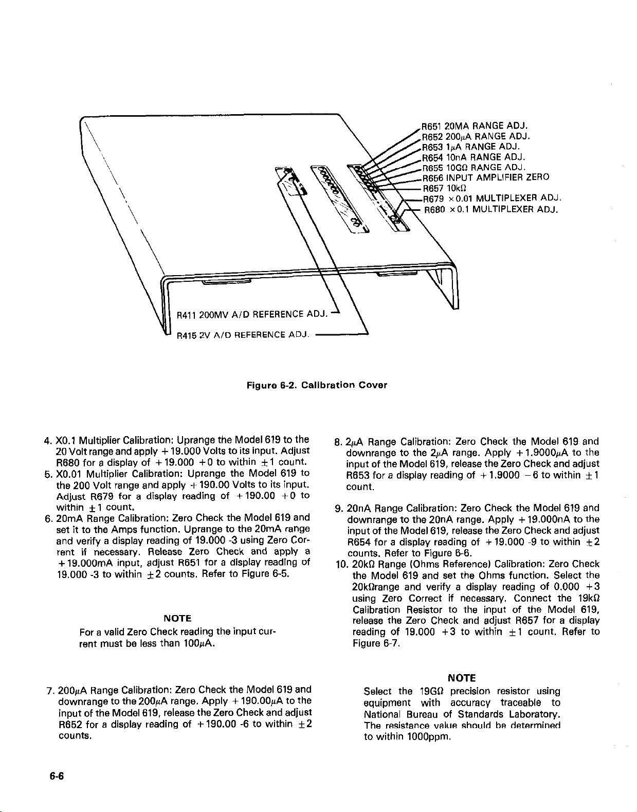
R41, 200MV A/D REFERENCE ADJ.
R415 2V A/D REFERENCE ADJ.
Figure 6-Z. Calibration Cover
R651 ZOMA RANGE ADJ.
R652 200pA RANGE ADJ.
R653 1AA RANGE ADJ.
R654 1OnA RANGE ADJ.
R655 1OGg RANGE ADJ.
R656 INPUT AMPLIFIER ZERO
Re7S x0.01 MULTIPLEXER ADJ.
R680 x0.1 MULTIPLEXER ADJ.
4. X0.1 Multiplier Calibration: Uprange the Model 619 to the
20 Volt range and apply + 19.000 Volts to its input. Adjust
R680 for a display of + 19.000 +0 to within f 1 count.
5. X0.01 Multiplier Calibration: Uprange the Model 619 to
the 200 Volt range end apply f 190.00 Volts to its input.
Adjust R679 for a display reading of + 190.00 + 0 to
within f 1 count.
6. 20mA Range Calibration: Zero Check the Model 619 and
set it to the Amps function. Uprange to the 20mA range
end verify a display reading of 19.000 -3 using Zero Corrent if necessary. Release Zero Check and apply a
+ 19.000mA input, adjust R651 for a display reading of
19.000 -3 to within *2 counts, Refer to Figure 6-5.
NOTE
For a valid Zero Check reading the input current must be less than 100&A.
7. 200pA Range Calibration: Zero Check the Model 619 and
downrange to the200pA range. Apply + 19O.OO~A to the
input of the Model 619, release the Zero Check and adjust
R652 for a display reading of + 190.00 -6 to within k2
counts.
6. 2&A Range Calibration: Zero Check the Model 619 and
downrange to the 2+A range. Apply + 1.9000/1A to the
input of the Model 619, release the Zero Check and adjust
R653 for a display reading of + 1 SO00 -6 to within rt 1
count,
9. 20nA Range Calibration: Zero Check the Model 619 and
downrange to the 20nA range. Apply + 19.000nA to the
input of the Model 619, release the Zero Check and adjust
R654 for a display reading of + 19.000 -9 to within *2
counts. Refer to Figure 6-6.
10. 20kQ Range (Ohms Reference) Calibration: Zero Check
the Model 619 and set the Ohms function. Select the
20kDrange and verify a display reading of 0.000 +3
using Zero Correct if necessary. Connect the 19kB
Calibration Resistor to the input of the Model 619,
release the Zero Check and adjust R657 for a display
reading of 19.000 +3 to within fl count. Refer to
Figure 6-7.
NOTE
Select the 19GQ precision resistor using
equipment with accuracy traceable to
National Bureau of Standards Laboratory.
The resistance value should be determined
to within IOOOppm.
6-6
Page 62

Figure 6-3. Supply Calibration .200mV
VOLTAGE SOURCE
MODEL 619
ELECTROMETER MODULE
REAR PANEL INPUT
--CC-
--cc
-5-J
TRIAX CONNECTION
TRIAX CONNECTION
MODEL 619
ELECTROMETER MODULE
REAR PANEL INPUT
MODEL 6011
INPUT CABLE INPUT CABLE
MODEL 601,
INPUT CABLE
<t
WAX CONNECTION
VOLTAGE SOURCE
Figure 6-4. Supply Calibration 2 Volt
CURRENT SOURCE
MODEL 6011 INPUT CABLE
Figure 6-5. Range Calibration 20mA
MODEL 619
ELECTROMETER MODULE
REAR PANEL INPUT
>’
L>
TRIAX CONNECTION
6-7
Page 63

11. 20GC Range Calibration: Calibrate the 20Gg range see
Figure 6-8. Zero Check the Model 619 and upranga
to the 20GQ range. Connect the 19G9 Calibration
Resistor to the input of the Model 619, release the Zero
Check, and adjust R655 for a display reading of 19.000
+ 9 to within f 15 counts.
12. Range Verification: After range calibration perform the
verification procedures. Refer to Section 3 for these
procedures.
13. Channel B Calibration: If a Channel B Electrometer is installed in the Model 619, Steps 1 and 4 through 12 must
be reoeated for this channel.
NOTE
Do not repeat Steps 2 and 3.
6.15 CALIBRATION FIXTURE
The required calibration fixture uses a source of 19Gg. Its
resistors must be accurate to 1000ppm.
1. The following items are necessary for proper calibration:
A. 2 lO.OGC resistors, Keithley part number R-289.IOG.
B. 1 lOO.OGC resistor, Keithley part number
R-289.100G.
C. 2 enclosed chassis boxes one to be placed inside the
other and insulated from each other.
D. 1 triax connector, Keithley part number CS-181.
E. 1 banana jack, Keithley part number BJ-Il.
F. 1 6191 Guarded Input Adapter.
G. 7024-l triax cable (1 ft long, male to male
connector).
r-------- -----------:
10M 10M IOM IOM IOM IOM 10M 10M 10M IOM 10M 1OMl 10M IOM IOM IOM IOM 10M 10M 10M IOM 10M 1OMl
II
/!I+fKyTj;;:
Figure 6-6. Range Calibration, 20nA
r-------- -------
SR-1010 CONFIGURATION FOR 19kg RESISTOR
SRI050 CONFIGURATION FOR IOOMD RESISTOR
TRIAX CONNECTION
A
Y 0
6-8
-----------___
90k
MODEL 619
ELECTROMETER MODULE
REAR PANEL INPUT
Figure 6-7. Range Calibration 20k0
MODEL 6011
i
TRIAX CONNECTION
INPUT CABLE
Page 64

NOTE
Possible scurces of high value resistors are:
Dale Electronics, Inc., Columbus, Nebraska
Victoreen. Cleveland, Ohio K b M Electronics, West Springfield, Massachusetts.
2. Refer to Figure 6-9 for a schematic of the calibration
fixture.
Once the value of the 19GO source has been established, it
may be used (for calibration) for a limited time. The stability
specifications of the resistors used will determine the length
of time the 19Go scurce can be used. After this time, the exact value of the 1.9GQ sowce must again be determined.
The teraohmmeter can be used to reestablish the value.
6.16 TROUBLESHOOTlNG
6.16 CONSTRUCTION INFORMATION
1. To decrease settling time and to assure accurate calibration, an internal guard is recommended (see Figure 6-9).
The guard must be isolated from the surrounding case.
2. To further minimize inaccuracies, current leakage paths
to ground (or guard) must be minimized. This requires
the use of low leakage insulating materials (such as
Teflon@ ) for construction and the use of special cleansing agents (such as Freon) to clean the components and
insulators after construction.
6.17 CALIBRATION of 1.9GQ SOURCE
Connect the 19GO source to a teraohmmeter. A meter with
acceptable accuracy is listed in Recommended Test Equip-
ment, Table 6-2). Determine the value to within *lOOO
ppm. This must be done at a temperature of 23°C f 1%
The troubleshooting information in this section is intended
for use by qualified personnel who have a basic understand-
ing of the analog and digital circuitry used in a precision test
instrument. Instructions have been written to assist in
isolating the defective circuit. Isolating the defective component has been left to the troubleshooter.
NOTE
For instruments that are still under warranty
(less than 12 months since date of
shipment), whose performance is outside of
specifications at any point, contact your
Keithley representative or the factory before
attempting troubleshooting or repair other
than battery or fuse replacement.
6.16.1 Special Handling of Static Sensitive Devices
CMOS devices are designed to function at high impedance
levels. Normal static charge can destroy these devices.
Table 6-3 lists all the static sensitive devices for the Model
619. Steps 1 through 7 provide instruction on how to avoid
damaging these devices.
SHIELDED TEST FIXTURE
----_
ii-
L - _ - _ -dim/
----
TRIAX CABLE
AA
' I
Figure 6-6. Range Calibration, 20GO
ANALOG OUT
(GUARD
CONNECTION)
619
>t
>t
>>-
>>
MODEL 619
ELECTROMETER MODULE
REAR PANEL INPUT
6-9
Page 65

Table 6-3. Static Sensitive Devices
6.16.2 Troubleshooting Procedure
Reference Designation
lJ202
Keithley Part Numbal
IC-141
U204, U207
lJ807
u905
U906
u907. u915. u924
u913.
u919, u920, u922, u923
LSI-28
LSI-27
PRO-114-•
PRO-1 15.”
LSI-26
LSI-15
1. Devices should be handled and transported in protective
containers, antistatic tubes or conductive foam.
2. Use a properly grounded work bench and a grounding
wriststrap.
3. Handle device by the body only.
4. PCB’s must be grounded to bench while inserting
devices.
5. Use antistatic solder suckers.
6. Use grounded tip soldering irons.
7. After devices are soldered or inserted into sockets they
are protected and normal handling can resume.
1. General Procedure
A. Turn the Model 619 ON.
B. Observe the proper indication on the display.
(a) Initially the display is blank and the beeper
sounds for approximately two seconds.
(b) Display shoes line frequency and level of the
software e.g. F60 C-l.
(cl The Model 619 ends up in the default conditions
e.g. Volts, Channel A, Zero Check.
C. Visually inspect all PC Boards to verify that they are
properly seated in the connectors.
2. Power Supply Checks
A. J305 pins 1,2,3,4 referenced to analog common has
33VAC f5%.
B. J305 oin 8 referenced to analoa common has + 15V
*5%:
C. J305 pin 9 referenced to analog common has -15V
+5%.
D. J305 pin 10, 11 and 12 referenced to analog common
has +5V f5%.
E. J304 pins 6,7,8 and 9 referenced to analog common
has +9.5V f5%.
F. Check each PC Board for appropriate voltage as
shown on the schematic diagram.
lOOGO
I
1. To decrease settling times and to assure
accurate calibrations. it is recommended
to use an internal guard (as shown in the
drawing abovel. The guard must be insulated from the surrounding case.
2 .To further minimize inaccuracies, current
leakage paths to ground for guard1 must
be minimized. This requires the use of low
leakage insulating materials (switches1 for
construction and the use of special cleansing agents such as freon@ to clean the
components and inwlators after construct
tion.
CONNECTOR
BANANA JACK
6-10
Figure 6-9. Calibration Fixture Schematic Diagram
Page 66

TRIAX RECEPT.
HI
---------
6191 ADAPTER
TRIAX PLUG
GUARD
UNGUARDED
NOTE: TRIAX RECEPT. IS INSULATED FRO,“,
CASE WHICH IS GROUNDED
THRU TRIAX PLUG.
Figure 6-10. Model 6191 Guarded Adapter
ANALOG OUTPUT
I
TO 619
3.
Clock Checks
A. CPU Borad (PC-5181, U905 pins 38 and 39 has 4MHz
at a TTL level.
B. A/D Board (PC-5201 Y501 has 4.915MHz. U516
divides this frequency to 307.2kHz lU516 pin 7) and
614.4kHz (U516 pin 61.
4. Logic Section Checks (CPU Board)
A. Verify data transfer from chip to chip.
B. Verify address logic and timing.
5. Isolator and Filter MUX Boards
A. Verify data transfer through the opto isolators ATl-
AT4 on the Isolator Board.
8. Check various voltages on the Filter MUX Board as
shown in the schematic diagram.
C. Check operation of Channel A and Channel B relays.
6. AID Converter Checks
A. Check signal paths from the Filter MUX Board to the
A/D Board.
B. Check integrator Output (U506 pin 2) as shown in
Figure 6-11 integrator output waveform.
7. Electrometer Checks
A. Check feedback loops of U651,
B. Check switching order of feedback loops.
C. Check bootstrap supplies (Test Points).
8. Front Panel Operation
It is important to check the front panel opration because
it will help to isolate the problem as a result of the read
out on the display.
6.19 Fan Filter Cleaning
The Fan Filter must be kept clean. Dirt in the filter will
impede the air flow through the Model 619 and cause
overheating. It is recommended to periodically remove the
filter (FL-31 and use compressed air to clean it.
6-I 1
Page 67

Figure 6-11. Integrator Output Waveform
6-12
Page 68

SECTION 7
REPLACEABLE PARTS
7.1 INTRODUCTION
This section contains replacement parts information, com-
ponent location drawings and schematic diagram for the
Model 619. A cross-reference list of manufacturers is also
provided (see Table 7-l ).
7.2 PARTS LIST
Parts are listed alphabetically in order of their circuit
designations. Table 7-2 contains parts list information for
the Display Board PC-514. Table 7-3 contains parts list information for the Power Supply PC-515. Table 7-4 contains
IEEE Interface PC-517 parts list information. Table 7-5 pro-
vides parts list information for the CPU Board PC-518; while
Table 7-6 contains parts list information for the Isolator
Board. Parts list information for the AID Converter PC-520
is presented in Table 7-7. Parts list information for the Elec-
trometer Module PC-523 and PC-522 are provided in Table
7-E. Table 7-9 contains parts list information for the Filter
MUX Board PC-521. Table 7-10 provides parts list informa-
tion for the Fan assembly.
7.3 ORDERING INFORMATION I. Figure 7-9. Filter MUX Board 30352D
To place an order, or to obtain information concerning
replacement parts, contact your Keithley representative or
the factory. See inside front cover for addresses. When
ordering include the following information:
1. Instrument Model Number
2. Instrument Serial Number
3. Part Description
4. Circuit Description (if applicable)
5. Keithley Part Number
7.4 FACTORY SERVICE
If the instrument is to be returned to the factory for service,
please complete the service form which follows this section
and return it with the instrument.
7.6 SCHEMATIC DIAGRAMS AND COMPONENT
LOCATION DRAWINGS
Schematic diagrams and component location drawings
follow the rsplaceable parts list information contained in this
section.
1. Component Location drawings for the Model 619 are as
follows:
A. Figure 7-l. Mother Board 30411C
B. Figure 7-2. Display Board 32003D
C. Figure 7-3. Power Supply Board 32004D
D. Figure 7-4. IEEE Interface Board 30329D
E. Figure 7-5. Processor Board 32005D
F. Figure 7-6. Isolator Board 32006D
G. Figure 7-7. A/D Converter Board 30395D
H. Figure 7.8. Electrometer Module Board
30387D and 30391D
2. Schematic diagrams for the Model 619 are as follows:
A. Figure 7-10. Mother Schematic 30517D
8. Figure 7-11. Display Schematic 306150
C. Figure 7-12. Power Supply Schematic 30516D
D. Figure 7-13. IEEE Interface Schematic 30518D
E. Figure 7-14. Processor Schematic (CPU) 30519D
F. Figure 7-15. Isolator Schematic 3052OD
G. Figure 7-16. A/D Converter Schematic 30521D
H. Figure 7-17. Electrometer Module Schematic
30522D and 30523D
I. Figure 7-18. Filter MUX Schematic 30524D
7-l
Page 69

5;;
UAME AND ADDRESS
-B
Illen-Bradley carp.
Milwaukee, WI 53204
Table 7-1. Cross-reference List of Manufacturers
FEDERAL
SUPPLY CODE
01121
MFR.
CODE F
F-I i
IAME AND ADDRESS
:airchild Instruments
b
lountain View, CA 94043
FEDERAL
SUPPLY CODI
07263
-0
4nalo9 Devices, Inc.
Vorwood, MA OZOZG
CI
I\merican Components, Inc.
:onshohockcn, PA 19423
YP
4mphenol
Iroadvicw, IL 60153
,%xkman Instruments, Inc.
EC
Fulierton, CA 02634
KG
ierij Electronic, Inc.
NEW Cunbcrland. PA 17070
011
3omar Crystal CO.
Yiddlcspx, NJ flI11~46
RN
Rourns. Inc.
,liwrsidc, CA 92507
Comp”ne”ts, 1°C.
-I
i3iddeford, ME 04005
C u K Components, Inc
Watertown, MA 02158
AD
Cnddock
Riwrsidc, CA 92507
LR
Centralab Division
Milwaukee, WI
53201
24355
1429?
02660
1318il
22526
--
80294
06751
09353
I%47
7159"
G-E (
GKH (
H-l' 1
INT I
ITT I
KaM i
K-I k
I.-F I
FIAL r
MIP I
ilMM ;
;eneral Electric Co.
iyracuse, Ny 13201
irayhill. Inc.
.a Granqe, IL 60525
L
icwlett-Packard Co.
'ala Alto, CA 94304
r
;ntersil, Inc.
:upertino, CA 95014
(
ITT Semicondlrctor
I
~awrance, MA 01841
: n M Electronics Co.
E
linncapolis, MN 55435
:cithley Instruments. Inc.
c
:lcvcland, Ohio, 44139
.ittlc Fuse, Inc.
I
1~s Plairvs, IL GO016
431 l0ry
Indianapolis, IN 46206
4rpco. Inc.
I
Morristown. NJ 07960
3M Company
it. Paul,
MN 55101
03508
81073
50444
32293
15238
_-
80164
75415
90201
80031
--
OC
DT
OW
TS
LF
CT
nr
MC
RI
-
7-2
Corcom
Chica9", IL 60639
Cot".Coil Co., Inc.
Providencr, INI 029flS
Continental Wirt
Warminster, PA
CTS Corporation
Elkhart, IpI 46514
Dale Electronics
Colunbus, NE 68601
ElectrO-Cube, Inc.
San Gabriel, CA 91176
Electronic Devices, Inc.
Yonkers, NY 10710
EMC Industries, Inc.
Hatbor", PA 19040
Eric Technological Prod.
Erie, PA 16512
05245
71707
79727
71450
91637
14752
83701
50417
72982
401fX
30wnc1.s Grove, IL GO515
Ylon5ant.o
it. Louis. MO 63122
MOT 1
MIIR I
NAT
NEC
NIC Nichicon Corp.
NYT
PAT
Yotorola Srmi Products, Inc.
'hoenix, AL 85008
I
"lurata Carp. of America
I
!Imsford, NY 10523
National Semi Corp.
Santa Clara. CA 94086
NEC Microcomputer, Inc.
Lcxinqton, MA n2173
Chicago, IL 60645
Nytronics Components Group
3arlington, SC 29532
I
Pattison Supply Co.
Cleveland, OH 44125
27264
76541
04713
51406
27014
--
--
83125
--
Page 70

Table 7-1. Cross-reference List of Manufacturers lCont.1
7-3
Page 71

Circuit
Desig.
c201
Description
.l,,F, 5Ov, CerF
Table 7-2. Display Board PC-514 Parts List
-
Schematic
Location
514/81
PC-Board
.tem No./Location
3/G?!
Mfr.
Code
ERI
Mfr.
Desig.
GlZl-MO50
651.104M
Keithley
Part No.
C-237-.1
c202
c203
C204
C205
C207
C208
DS201
DS202
DS203
OS204
OS205
OS206
DS207
.luF, 5OV, CerF
.luF, 5OV, CerF
33vF, lOV, Tant
.lpF, 5OV, CerF
.l,,F, 5OV, CerF
lOOOpF, CerD
Digital Display tl
8 Segment Display
8 Segment Display
8 Segment Display
8 Sequent Display
8 Sqment Display
Digital Display rl
514iRl
514/51
514/A1
514/01
514/Bl
514lF4
514lEl
514/El
514lFl
514/Fl
514iF1
514/Fl
514fGl
4/03
5/c3
b/C3
7103
9lR4
lo/H3
14/A2
15lA2
16/A2
17102
18iB2
19/B2
2o/c2
ERI
ERI
C-I
ERI
ERI
ERI
F-I
F-I
F-I
F-I
F-I
F-I
F-I
8121-MO50
651.104M
RlZl-MO50
651.104M
TSD 3-10
336-PCM 1287
8121-MO50
651-104M
8121.MO50
651.104M
8012, 5V
472M
FND51fl2
FNrl5101
FND5101
FNDSlDI
FND5101
FND5101
FND5102
C-237-.1
C-237-.1
C-180-33
C-237-.1
C-237-.1
C-64-1000,
DD-21
DD-20
DO-20
DO-20
00-20
DD-20
DO-21
OS208
DS209
DS210
DS211
DS212
OS213
DS214
DSZi5
DS216
DS217
B Segment Display
LED, Red
LED, Red
LED, Red
LED, Red
LED, Red
LED, Red
LED, Red
LED, Red
LED, Red
514/Gl
514/F4
514/F3
514/F3
514/H2
514lF4
514/G4
514/Hl
514/F3
514fG3
21/c2
22/c2
23lC3
24lC2
25/A3
26103
27fC3
28/A3
29/B3
,3o/c3
F-I
MON
MON
MON
MON
MON
MON
MON
MON
MON
-
FND5101
MV5753
MV5753
MV5753
MV5753
MV5753
MV5753
MV5753
MV5753
MV5753
DO-20
PL-67
PL-67
PL-67
PL-67
PL-67
PL-67
PL-67
PL-67
PL-67
7-4
Page 72

Table 7-2. Display Board PC-514 Parts List (Cont.1
Circuit
lksig.
DSZIR
OS219
DS220
DS22 1
,DS222
US223
OS224
OS225
DS226
OS227
OSZZR
05229
LS201
R201
Description
LED, Red
LED, Red
I
LED, Red
LED, Red
LEO, Red
LED, Red
ILED, Red
LEU, Red
LEn, kd
LEO, Rfd
LEU, Red
LED, Red
Burrer
10k. 5%. 1/4W, Camp
I
Schematic
Locat ion
514/112
514/F3
514/G3
514/Hl
514tF4
514/G4
514/F3
514/G3
514lF3
514/G3
514/G3
514/H3
514/F4
514/c5
PC-Board
Item No./Loca
31lA3
32lR3
33/c3
34/A3
35/113
36lC3
37lB3
3R/C3
39/R4
'IO/C4
41/84
421C4
51/H3
55102
Mfr.
Cod1
MON
MON
MON
MON
MON
MON
MON
MON
MON
MON
MON
MON
MUR
A-B
Mfr.
Des i g.
MV5753
MV5753
MV5753
MV5753
MV5753
MV5753
MV5753
MV5753
MV5753
MV5753
MV5753
MV5753
PMlZ-6A0
EB
Keithley
Part No.
PL-67
PL-67
PL-67
PL-67
PL-67
PL-67
PL-67
PL-67
PL-67
PL-67
PL-67
PL-67
EM-3
R-76.10k
R202
R203
R204
R205
R206
R207
RZOB
R209
R-210
R211
R212
R213
R214
10k 5%, 1/4W, Comp
lOk, 5%. 114W, Camp
lOk, 59,, 1/4W, Camp
lOk, 5%. llilW, Camp
47, lo%, l/ZW. Comp
47, 10%. 1/2W, Comp
47, 10%. l/ZW, camp
47, 10%. 1/2W. Comp
47, IO%, l/ZW, Camp
47, 10%. IIZW, Comp
47,
lo%, l/ZW, Corn,
47,10%, l/ZW, Camp
47,10%, l/ZW, Comp
514/05
514/05
514IE5
514/F4
514lrll
514lLll
514lCl
514101
514/D
514IEl
514/01
514/01
514/E3
56/E2
57/F2
5BlG2
59jH2
6O/A3
61/A3
62lA3
63/A3
64183
s/o3
66/A3
67/A3
6RlA3
A-B
A-B
A-B
A-H
A-B
A-B
A-R
A-5
A-B
A-R
A-B
A-B
A-B
EB
Er?
EB
ER
EB
ER
ED
ER
EO
ER
EB
ER
EB
R-76-101
K-76-101:
R-76.IOk
R-76-1.5
R-1-47
R-1-47
R-l-47
R-l-47
R-1-47
R-l-47
R-l-47
R-1-47
R-l-47
7-5
Page 73

Xrcuit
ksig.
?215
Description
47,
10x, l/ZW, ComQ
Table 7-2. Display Board PC-514 Parts List (Cont.)
-
Schematic
Location
514/E3
Item
PC-Board
No./Location
69/D
Mfr.
Code
A -II
Mfr.
Desig.
ER
Keithley
Part No.
R-1-47
?216
R217
7218 4.7k, 5%, 1/4W, Comp
1219
X220 bBk, 5%, 1/4W, Comp
5201 Switch, Pushbutton
5202 Switch, Pushbutton
5203 Switch, Pushbutton
$204 Switch, Pushbutton
s2n5
SZOB Switch, Pushbutton
5210 Switch, Pushbutton
s211 Switch, Pushbutton
5212 Switch, Pushbutton
47, 10%. 1/2W, Camp
4.7k, 5%. 1/4w, camp
4.7k. 54, 1/4W, Conl,
Switch, Pushbutton
514/E3
514IE3
514lE3
514/E3
514iE2
514/c5
514105
514/u5
514lE5
5l4/C5
514/E5
514/05
514/E5
514/E',
70103
7llC3
72lC3
73lC3
74/C3
RI/II2
RZ/EZ
83/F2
R4/G2
85/02
IIR/GZ
9O/E3
91/F3
92/G3
A-R
RRN
DRN
BRN
RRN
SCll
SCH
SW
XII
SCH
SCH
SC,,
Scti
SCH
ER
CR25,4.7k,
1%. 1/4w
CR25, 4.7k
lo%, 1/4w
CK25, 4.7k
lfl%n, 1.4w
MDP
MUP
M"P
MDI'
MliP
M",'
MOP
MDP
MOP
K-l-47
R-76-4.7
R-76-4.7
R-76-4.1
R-76.68K
SW-435
SW-435
SW-435
SIJ-435
SW-435
SW-435
SW-435
SW-435
SW-435
S213 Switch, Pushbutton
5216 Switch, Pushbutton
5217 Switch, Pushbutton
5218
5219 Switch, Pushbutton
5220
Switch, Pushbutton
Switch, Pushbutton
514/c5
514/E5
514li6
514106
514/06
514lE6
93/03
96/G3
97103
9R/E3
99/F3
lOOIG4
SCH
SCH
SCH
SCH
SCH
SCH
-
MDP
MDP
MDP
MDP
MOP
MDP
SW-435
SW-435
SW-435
SW-435
SW-435
SW-435
7-6
Page 74

Table 7-2. Display Board PC-514 Parts List NXmt.)
Circuit
Desig.
Mfr.
CO&
scii
I-I
Nil
r-1
,,I,1 ,
I-I
I:
WI
7-7
Page 75

Table 7-3. Power Supply PC-515 Parts List
Circuit
Desi g.
c301
c302
c303
c304
c305
C306
c307
C3OB
c309
c310
c311
c312
co- 7
CR301
kscription
.Oli,F, 5oov, ccrn
116001~F, 25V, Alum Elect
llfiOn,,F, 25V. Alum Elect
lOuF, ZOV, Tant
lO,,F, ZOV, Tant
lO,iF, 2OV, Tant
l&F, 2OV. Tant
52O,,F, 35V, Electrolytic
620uF, 35V, Electrolytic
68OO,,F, 25V, Alunl Elect
lO,,F, ZOV, Tant
10,li. 2nv, 'rant
3 Wire Line Cord
Rcctificr, Bridge
Schematic
Location
515105
515/E4
515/E4
515/E3
515lE3
515/E2
515iE2
515/E3
515JE2
515/E4
515/E4
515lE4
.-
515/o/1
PC-Board
Item No./Location
3/c5
4lC5
5/c5
6/F3
7lF4
B/F4
9/F4
IO/F5
II/F5
12/G4
13/G4
14/G5
-/A5
17/c4
Ifr.
:ode
jPG
1IC
IIC
ITT
ITT
ITT
ITT
1IC
?IC
RIC
ITT
ITT
PAT
--
Mfr.
Desig.
B7I-z5uo
103M
HC9-11-11600
25.8P
HC9-11-11600
25.BP
Tap/FOIOF200
Tap/FOlOFZOO
Tap/FOIOFZOO
TapIFOIOFPflO
HC-SC-620
35-RP
K-SC-620
35.8P
HCP-I-6800
25.8P
Tap/FflOFLOO
TaplFOIOF200
--
--
(eithley
?art No.
:-22..Ol
C-314-11600
C-314-11600
c-179-10
c-179-10
c-179-10
c-179-10
C-309-620
C-309-620
C-314-6800
c-179-10
c-179-10
co-7
RF-51
CR302
CR303
F301
F301
J302
J303
5304
5305
5306
5307
P301
P302
P303
Rectifier
Rectifier
Slow 1110~ 250V lA/3AG
Slow Blow 25OV. 1/2A/3AG
Molex
Molex
Molfx
Molex
Filter, Power line
Molex, Male
Molex, Male
515/114
515/1)2
515/w
515/B3
515lC5
5151132
515/F4,5
515/F2,3
515lA3
515K5
515/R2
IBIG
19,G5
ZI/A,B 4
22/A,B 4
_.
--
23/ll3
24lG3
26/B5
27103
28/B5
ED1
EDI
L-F
L-F
MOL
MOL
MOL
MOL
cot
MOL
MOL
PE05
PF-40
MDL
MDL
09-50-3031
09-50-3031
09-52-3102
09-52-3102
6EFl
A-2391-3A
A-2391-3A
RF-48
RF-46
FU-10
FU-4
K-287-3
C-287-3
CS-332-12
CS-332-12
cs-249
cs-249
LF-2
CS-288-3
CS-288-3
7-8
Page 76
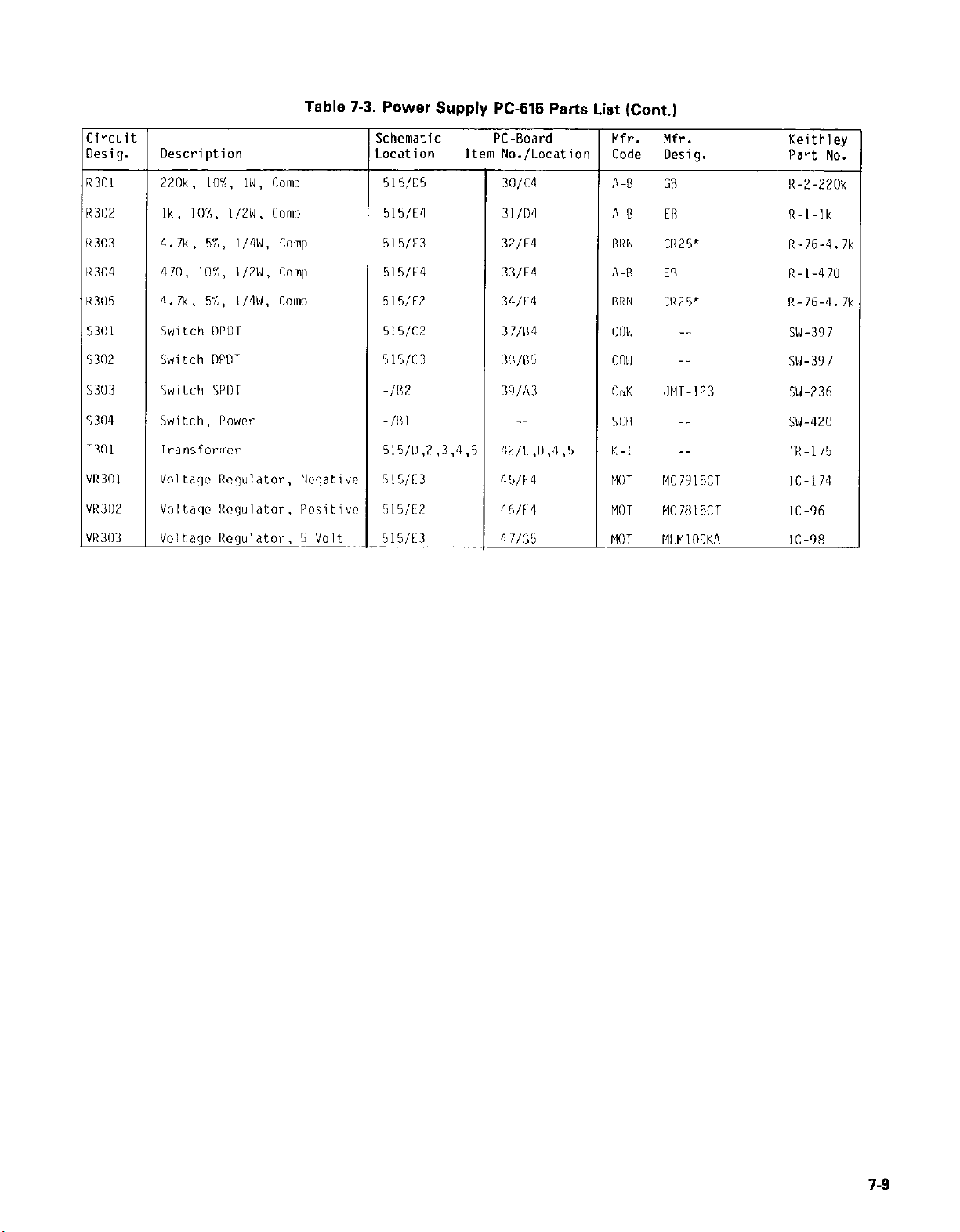
Table 7-3. Power Supply PC-515 Parts List Kkmt.)
Circuit
Oesig.
11301
K302
11303
113”4
113E
53111
s3n2
5303
53n4
7301
VI1301
VK302
VK303
Description
22flk. 10%. lW, Camp
Ik. 10%. l/ZW. Camp
4.?k, 5X, ll4W. Comp
47n, 10%. l/ZW, Camp
'1.2x, sii, 1/41d. camp
Witch 111'0 r
Switch DPDT
Switch SPIIT
Switch, Power
rransformcr
Vnltaqc Regulator. Ilvqativ~
Vnltaqr RCYuldtor, Positivr
vo1taqr IRcqulator. 5 Volt
ichematic
1
acation
T
515/D5
515lE4
515/E3
515,E4
515,FZ
515,CZ
515/C3
-IN2
I!3 1
515/11.2.3.4,5
515/1:3
515/EZ
515/t:3
PC-Board
Item No./Locatior
3ll/C4
31m4
32/F4
33/F4
34/i-4
37lli4
:38/B’,
3'31,13
.~
42/i: .“.,I .5
45li4
4hli4
4 7,E
Mfr.
Code Desig.
A-B GR
A-B CR
RIIN CK25*
A-R ER
RRN
cow
cm1
CaK JMT-123
SCH
K-I
MOT
MOT
MOT MLM103KA
Mfr.
m75*
--
MCIYLICT
MC7815Cl
Keithley
Part No.
R-2-220k
R-1-lk
R-76-4.7k
R-1-470
R-16.4.7k
SW-337
SW39 7
SW-23h
SW-420
TR-175
lC-174
IC-96
IC-98
7-9
Page 77

Table 7-4. IEEE Interface PC-517 Parts List
:ircuit
lesi g.
:701
:702
:703
:704
:705
:706
:707
Z708
c 709
c710
kscription
.luF, 5OV, CerF
.luF, 5OV, CerF
.luF, 5OV, CerF
.lpF, 5OV, CerF
.luF, 5OV, CerF
.luF, 5OV, CerF
.l,)F, 5OV, CerF
.luF, 5OV, CerF
.lpF, 5OV, CerF
.1uF, 5OV, CerF
r
Schematic
Location
5!7/Al
517lAl
517/Bl
517/01
517/Bl
517181
511lBl
517/Cl
517/Cl
51 T/Cl
PC-Board Mfr.
Item No./Location
3/c4
4/c4
5ic5
6104
7104
H/E4
9/04
IO/E4
ll/F4
12lF4
Code
ERI
ER I
ERI
ERI
ERI
ERl
ERI
ERI
ERI
ERI
Mfr.
Desig.
r
8121.M050651-104M
8121-MO50-
651.104M
8121.M050651-104M
8121-M050-
651.104M
8121.MOW
651.104M
8121-M050-
651-104M
X121-MO50
651-104M
RlZl-M050-
651.104w
8121.Mn50-
651.104M
8121.M050-
651.104M
Keithley
Part No.
C-237-.1
c-237-.1
C-237-.1
C-237-.1
c-237-.1
C-237-.1
C-237-.1
C-237-.1
C-237-.1
c-237-.1
c711
c712
c713
5701
R701
s701
u701
U702
u703
u700
u705
U706
.l,iF, 5OV, CcrF
lOuF, 25V, Alum
22eF, 25V, Alum
Right Angle Mount Rect
Thick Film
Dip Switch
Bus Transceivers
Bus Transceivers
Buffer/Line Driver
Bus Transceivers
Bus Transceivers
GPIA
517iCl
517lR6
517/R6
517/G2,3,4,5
517/01
517/El
517/F5
517lF2
517185
517/F4
517/F3
517/E
13/F5
14lG4
15/G5
19/R4
20105
21/85
25/C4
26/D4
27lC5
28lC4
29/C4
3O/D,E4
ERI
ITT
C-I
AMP
RIIN:
CTS
MOT
MOT
MOT
MOT
MOT
MOT
8121.MO50
ii'll-104M
TAPirnln, FZOO
TSO3-lo-336
PCM1287
552791-1
4308R-101-223
206-7
MC344RA
MC3448A
74LS244
MC3448A
MC344GA
68488
C-237-.1
C-314-1(
C-314-22
cs-377
TF-100
SW-377
IC-193
IC-193
IC-230
IL193
IC-193
LSI-14
7-10
Page 78

Table 7-4. IEEE Interface PC-517 Parts List Khnt.1
Circuit
Desig.
u707
” 708
U7OY
U?lO
u711
VR701
Description
Hex Inverter
Triple-3 Input Nand
Hex-3 state
Quad Bus Rxcivers
Quad iBus Receivfrs
5 "nit Requlator
IRUffW
Schematic PC-Board Mfr.
Location
5, IISEV 31/114 MOT
5, llst~v
517/1)2
‘51 71114
5, 1/112
5, ,,,I6
Item No./Location Code
32lE4
33/F4
14/14
35,,~!,
3 i/G5
MOT
MOT
MOT
MO1
MC r
Mfr.
Desi 9.
741sn4
74,.Sl”
74LS367
YT26
8726
MC IR"5
Keithley
Part No.
IC-186
IC-155
IC-161
IC-IRO
IC-180
IC-93
7-11
Page 79

Table 7-5. CPU Board PC-518 Parts List
Circuit Schematic
Desig.
c901 .l,,F, 5OV, CerF 51m5 3lR2 ERI 8121-MO50-
c902 .l!J, 5ov, CErF 51HiR5 4lC2 ERI 0121-MO50- C-237-.1
c903 .l,,F, 5OV, CerF 51RIt35 5lC2 ERI 8121.M050- C-237-.1
c904 .luF, 5OV, CerF
c905 .l,,F, 5OV, CcrF
C906 .luF, 5OV, CerF 51ii/n5 8/F2
c907 .luF, 5OV, CcrF 518/115 O/B2
C908 .luF, 5OV, CfrF 518/r% lO/RZ
c909 .luF, 5OV, CerF 518/05 II/U2
c910 ZZpF, lOOOV, Cer" 518/W 12/02
Description Location Item No./Location Code Desig. Part No.
SlR,iiS
51R/B5 7IF2
PC-Board
b/E2 ERI RlZl-MO50- C-237-.1
Mfr.
ERI 0121.MO50- C-237-.1
ER I HlZl-MO50- C-237-.1
ERI X121-MO50- C-237-.1
ER, 8121.M050- C-237-.1
ERI 8121.MO50- C-237-.1
EilI 838-000-u230-
Mfr. Keithley
C-237-.1
651.104M
651.104M
651.104M
651-104M
651.104M
651-104M
651.104M
651.104M
651-104M
C-64.22pF
22OK
c911 22pF, 1ooov, ceru 518/112 13/02
C912 .luF, 5OV, CerF 5lH/D2 14lF2
c913 .l,,F, 5OV, CerF 518/C5 15/A3
c914 .l,,F, 16V, CerD 51H/D2 16/B3
c915 .OluF, 16V, Cern
C916 .luF, 16V, CerD
c917 .l,,F, 5OV, CerF
CY18 2211F, 25V, Alum
c919 .luF, 5OV, CerF
c920 .luF, 5OV, CerF
c921 .l\f, 5OV, CerF
51WE2 17/R3
51H/E2 1x/03
51RIC5 19/03
518/A5 20/113
SlS/CS 21/E3
518/C5 22lE3
51w5 23/E3
ERI 83X-000-11250
ERI HlZl-MO50- C-237-.,
ERI
CLB UK16-104
CLR UK16-103 C-238-.0:
CLR UK16-104 C-238-.1
CLR
ITT
CLB H121-MO50-
CLR 8121-MO50-
CLB
220K
651.104M
8121.MO50
651-104M
RIZI-M050- C-237-.1
651.104M
TAPIFOZZ, FZOU C-314-22
651.104M
651-lg4M
8121~MO50
651.104M
C-64.22Pf
C-237-.1
C-238-.1
C-237-.1
C-237-.1
C-231-.1
7-12
Page 80

Table 7-5. CPU Board PC-518 Parts List (Cont.1
Circuit
Desig.
c922
c923
c924
'CR901
R9Ol
R902
Rg"3
u901
u902
u903
u904
u905
U906
Description
.luF, 5DV, CerF
lOuF, 25V, Alum
.iuF, 5OV, CerF
Diode, Silicon
Thick Film
lM, 5%, 1/4W, Comp
lM, 5%. 1/4W, Camp
Buffer/Line Driver
Dual 4 Jnput Nand
Dual 4 Input Nand
Triple-3 Input Nor
Microprocessor with clock
PROM
schematic
I
acation
518/E 24/F3 CLB
PC-Board
Item No./Location
t
51H/R5
518/C5
518/E1
518/A,B
518/El 41/A3 MEP
51R/E2 42/R3
518/C4
518lB3.4
518/05,6
51R/D4,6
518/D1,2,3,4
51R,F4
25103 C-I c-314-11
26/E3 CLR C-237..
32/A3 T-I
4O/C2 RRN
h5lA2 YOT IC-230
66/52 YOT IC-232
67lC2 YOT IC-232
6RIC2
69/D,E,2 YOT LSI-27
70/E? INT
Mfr.
Code
T
Mfr.
Desig.
8121-M050-
651-10411
TSO3-IO-336
PCM-1287
8121.M050651-104M
IN914
4306R-101-332
CR25*
MEP R-76.1M
YOT
CR25*
74LS244
SN74LS20
SN74LS20
SN74LS27
MC6008
2716
Keithle:
Part No
C-237..
RF-28
TF-101
R-76-1M
IC-233
*i
PRO-114
u907*
uson
1,909
u910
u911
u912
u913
u914
u915
U916
u917
U918
u919
PROM
Buffer/Line Driver
Hex 1nvcrter
Iriple-3 Input Nand
Hex-3 State Ruffer
Quad-2 Input Nand
Programmable Module Timer
Decoder/Multiplexer
PROM
Quad-2 Input Nand
Timing Circuit
Quad Bus Receivers
Static RAM
51D/E4
518/C3
518/SEV 73lR2 4OT
51X/05
518/C5
518/SEV
51X/02,3
518/04
518/F3
518/SEV
518/E2
518/C2
51t3fE2
7llF2 INT PRO-II;'
72/A2 YOT IC-230
74lC2 T-l IC-155
75/A2
76182
?7/C3
78/C2 SIG IC-190
79lF2
DO/A3 ti"T IC-231
al/B3 SIG IC-71
82/C3 SIG IC-180
83fE3 VEC LSI-15
--,
4OT
+lOT LSI-26
INT
2716
74LS244
74LSO4
74LS14
74LS367
74LSOO
MC6R40
SN74LS139
2716
SN74LSO3
NE555
8726
2114
IC-I56
IC-161
IC-163
PRO-115'
*Manufacturers Designation includes parts description, e.g., CR25, lM, 5%. 1/4W, Comp, and R903.
**Order same as current software level displayed on power-up. For example, if Cl is displayed, order PRO-1 14X1.
7-13
Page 81

Table 7-5. CPU Board PC-518 Parts List (Cont.1
Circuit Schematic
lesig. Description
J920 Static RAM 518/El
u921
u922 Static RAM 518/F2 86/E3
u923
u924*
VR201 5.Volt Regulator 518/E3
VR901 5-Volt Regulator 518/85
Y901
TPI Test Point E5 48102
TP2
TP3 Test Point E5 SO/D2
TP4
TP5
TP6 Test Point C6 53/C2 K-I
Quad Bus Receivers
Static RAM 518/Fl 87/E3
PROM 518/E3
4MHZ Crystal
Test Point E5
Test Point F5
Test Point
Location Item No./Location
51R/Cl
518/02 llllE2 CTS MP040 CR-10
E5 52103 K-l
PC-Board Mfr. Mfr.
84/E3 NEC 2114
85/C3
88/F3 INT 2716
93/D3
94/03 MOT MC7805
49102 K-I c-339-4
51102 K-I
Code Desig.
SLG
NEC 2114
NEC
MOT
K-1 ___
K-, ___
8T26
2114
MC7805
Keithley
Part No.
LSI-15
IC-180
LSI-15
LSI-I5
PRO-l15*
IC-93
IC-93
cs-339-4
cs-339-4
cs-339-4
24249A
cs-339-Z
TP7
TP8
TP9
TPlO
TPll
TP12
w901
w902
w903 Jumper 06 99/62
w904
w905
W906
w907
W908 Jumper
w909 Jumper
*Populated in PC-518 when 11906 and 11915 are 2716's.
Test Point C6 54/c3 K-I
Test Point 65 55102
Test Point 65
Test Point
Test Point 61
Test Point 82 59/c3
JUmpW
JUllpW
Jumper
JUmpW
JUllpW
Jumper
A2
G4 97102
D5
05
D5
E5 102/62 J-3
06 103102
65
G4 105lF3
56/02 K-I c-339-2
57/n
58/C3 K-I cs-339-3
98102
loo/c2 J-3
lOl/C2 J-3
104/83
cs-339-2
K-I cs-339-2
K-l es-339-z
K-1 -_-
___ _-__. .._
___ ___
___ ___
__- -._
cs-339-3
J-3
J-3
J-3
J-3
J-3
J-3
Page 82

Table 7-8. Isolator Board PC-519 Parts List
Circui.
Desig.
CEO1
C802
CR03
C804
LB05 .l,,r, 5ov, cd
:806 .luF, 5OV, CerF
XXI7
308
x09
2310
Description
.l,rF, 5OV, CerF
.luF, 5OV, CerF
.luF, 5OV, CcrF
.luF, 5OV, CcrF
22uF, 25V, Alw
.luF, 5OV, CrrF
.I,rF, sow, Cerl
Schematic
Location
519/Rl
519/81
519/Rl
519/Bl
519/Rl
519/Rl
519/ill
519/Al
51OiG5
519/m
PC-Board
Item No./Locatior
3lR2
41112
5jl32
6lR2
7182
ii/l32
9/c2
lO/C3
II/F2
12/E2
Mfr.
Code
ERI
ERI
Et?1
ERI
ERI
C-I
ITT
EKI
EKI
Mfr.
Oesig.
8121-M05D-
651.104M
8121.M050-
651.104M
8121.M050-
651.104M
8121-M050-
651.104M
8121.MD!&
651.1114~
RlZl-M050-
651.104~
7503.IO-
336, PCM12R7
TAD/FOlfl, F200
RlZl-MD50-
651LlO4M
8121.M050-
651.1114M
Keithley
Part No.
c-237-.1
c-237-.1
c-237-.1
C-237-.1
C-237-.1
C-237-.1
c-314-10
C-314-22
C-237-.1
C-237-.1
-
Xl1
:812
:813 .l,,F, IhV. CcrD
:814 .l,lF, 168, tern
:815 . I,5 , 16V * cero
:R16
x17
X18
:819
:R801
:R802
:R803
:R804
.l,,F, sov, CerF
.l,,F, 5OV. Ccri-
22uF, 25V, Alun,
.l,,F, 5OV, CerF
.luF, 16V, CcrD
.l,,F, 5OV, CerF
Rcctificr
Rectifier
Kcctifier
Rectifier
519/a
519/E
519/E5
519/E4
519113
519/G5
519/G’,
519/E2
519/111
519lAb
519iA6
519/A6
519/A6
13/E2
14lE2
19/F2
2O/F2
21/c3
79/D2
110102
RI/D2
82lD2
ER,
ER I
ERI
CL0
Eli I
T-I
T-I
T-I
T-I
iilZI-MO50
651-lfl4M
RlZl-MD50-
651.104M
UKl6-104
IJKlG-104
"KlG-104
TSU3-IO-
336, PCMlZI37
8121-M050m
651-104M
IIK16-104
8121.M05fl-
651.104M
lN914
IN914
lN914
lN914
C-237..
C-237-.1
C-238-.1
C-238-.1
C-238-.1
C-314-22
C-237-.1
C-238-.1
C-237-.1
RF-2R
KF-28
RF-28
RF-2R
1
'801
1801
I802
connector
Thick Film
270. 5%. 1/4W, Camp
519/A
519104
519/E3
23/G2
25/B
26/F2
3M
1
i1R N
IjRN
3429.2002
430, RRlOl-223
Cl<25*
CS-322-26
TF-100
R-76-270
z
7-15
Page 83

:ircuit
big.
lescription
Table 7-6. Isolator Board PC-519 Parts List ICont.)
l-
<
Zhematic
1
mation
PC-Board
Item No./Locat.ion
Ifr.
:ode
Mfr.
Desig.
Keithlq
Part No.
1803
:804
\805
1806
(807
1808
1809
la10
$801
JUOI
J802
J803
11004
J805
!70, 5x, 1/4w, camp
270, 5%, 1/4W, Comp
390, 54, 1/4W, Comp
390, 5%, 1/4W, Comp
390, 5%, 1/4w, Comp
IOk, 5X, 1/4W, Comp
390, 5X, 1/4W, Comp
270, 54, 1/4w, camp
Switch
HEX 1nvertcr
Decoder/Multiplexer
Ruffcr/Linc lirivcr
Triple-3 Input Nand
Quad Rus Receivers
519/G!
519114
519/Dl
519/E4
519/E3
519/F]
519lE2
519/Ei
519lD3
519/SEV
519iA5
519/A4
519/SEV
51')/A2
21/F2
2R/F2
29/F2
3O/F2
3I/F2
32/F?
33/F2
34/F2
39/Rl
43/A2
441A2
45lA2
46/R2
47fR2
1RN
IRN
IRN
INN
RN
RRN
RRN
RRN
Gilli
MOT
SIG
MOT
T-I
SIG
CR25*
CR25*
CR25*
CR25*
CR25*
CR25*
CK25*
1X25*
76SR04
74LSO4
SN74LS139
74LS244
74LSlO
0726
K-76-27(
R-76-271
K-76-391
R-7b-391
R-76-391
K-76-101
R-76-391
R-76-271
SW-422
IC-186
IC-190
IC-230
IC-155
IC-la0
U806
UH07
UBO8
U809
LIB10
U811
U812
U813
U814
U815
U816
*Manufacturers Designation includes parts description, e.g. CR25, 390, I%, 1/4W, Camp for R810.
Quad Bus Receivers
Versatile Interfacr Adapt?
Shift Register
Quad-2 Input Nand
Quad-2 Input Nor
Odd/Even Parity Generator
Checker
Shift Register
Quad-2 Input Nand
Odd/Even Parity Generator
Checker
Shift Register
&Bit Parallel Serial Cow
r
519/A3
519/C
511/1)2
519/SEV
519/w
519iF3
519/F3
519/w
519/F4
519/F2
519/FI
48/112
49K2
so/c2
51/C2
52/02
53102
54102
55/E2
56/E2
57lE2
58/F2
SIG
SYN
T-I
T-I
SIG
T-I
T-l
T-l
T-I
T-l
MOT
8'121,
SYP6522
SN74LS164
SN7400N
74LSO2
74LS2RO
SN74LS164
SN740ON
74LS280
SN74LS164
74LS165
IC-IlNl
LSI-28
IC-L27
IC-38
IC-179
IC-236
IC-I27
IC-38
IC-236
IC-127
IC-237
7-16
Page 84

Table 7-6. Isolator Board PC-519 Parts List ICont.)
Circuit
Desig. Description Location
AT1 Opt0 Coupler 519/E5
AT2 opt0 Coupler
AT3 Opt0 Coupler
AT4 Opt.0 Coupler
VRROl 5 Volt Regulator 519m2
Schematic
519lE4
519lE3
519iCl
PC-Board Mfr.
Item No./Location Code Desi g.
Gl?/FZ H-P HCPL-2601
69/F2
7O/F2
71/G2 H-F
75lD2
II-P CCPL-2601
H-P HCPL-2601 IC-239
F-I
Mfr. Keithley
HCPL-2601
Sli323SC IC-240
Part No.
IC-239
IC-239
IC-239
7-17
Page 85

Table 7-7. A/D Converter PC-520 Parts List
Circuit
Desig.
c501
C502
c503 .l,,F, IGV, CcrD
c504 .luF, 16V, CerD 520/H5 h/E2
c505 .l,,F, 16V, CerD
C506 .LpF, 16V, CcrD 520/F] R/C3
c507 lOOpi, IOOOV, CerD 52D/Gl 9lC3
C508 .luF, 16V, CerD 52O/Gl IO/C3
c509 IDDpF, lOOOV, CcrD 520/F2 II/C3
c510 .luF, 16V, CcrD 52D/El 12/D3
c511 .luF, 16V, CerD 52D/H5 13lD3
C512
c513 .l,,F, 5OV, CcrF
c514
Description
.luF, 16V, CerO 520/115 3/u%
36OOpF. lOflOV, CcrD 520//E 4/c2
.luF, 5OV, CcrF 52O/H5 14/E2
.luF, IhV, CerD 520/H', 16/E3
Schematic PC-Board
Location
520/H5
520/H!,
520/H5 15/E2
Item No./Location
5iEl
7iF2
Mfr. Mfr.
Code Desig.
CLR UKIG-104
CLD 5% MAL C-138.36DOpF
CLR UK16-104 C-238-.1
CLB tlK16.104
CLB UK16-104 C-238-.1
CLR UK16-104 C-238-.1
CRI. 00-101 c-64-1OOPF
CLR tlK16-104
CRL DD-lnl C-64.100pF
CLR UK16-104 C-238-.1
CI.R UK16-104 C-238-.1
El< I 8121M050651104M C-237-.1
EKI
CLR UKlb-104 C-238-.1
36OOpF
8121M050651104M C-237-.1
Keithley
Part No.
C-238-.1
C-238-.1
C-238-.1
L501 Choke 52fllFl 19IC3 NYT SWD-100
q501 N-Channel J-FET
q502 Transistor Array
4503 NPN Transistor 520/A3 23/C2
q504 PNP Transistor
4505 PNP Transistor 52fl/Rl 25/R2
Q506 PNP Transistor
4507 Transistor Array 52D/Cl 27lC2
QSOU N-Channel J-FET 520/Gl 28lC3
4509 NPN Transistor 520106 29/E3
0510
R501 Thick Film 52O/Several 33102
R502 Thick Film
R503
PNP Transistor 520182 30/Rl
6.8M, IO%, 1/4W, Comp 520105
520/l?& 211131
520/4A 22/c2
52O/A2
52O/Cl 261132
520/Several 34/C2
24IC2
35/83
INT
K-I 29190/l
MO'I 2N3904
F-l
F-I 2N363RA TG-84
F-I 2N3630A
K-I 29198A 29198A
INT ITE4392 TG-77
MOT 2N3904 TG-47
F-I 2N3638A TG-84
OLE TF-06 TF-86
DLE TF-85 TF-85
DLE
I~TE4392
2N3638A
CK25* R-76.6.OM
u-14
TG-77
2919RA
TG-47
TG-84
TG-84
7-10
Page 86

Table 7-7. A/D Converter PC-520 Parts List ICont.1
Circuit
Desig.
R504
R505
R506
R507
R508
R509
K510
11501
U502
u503
u504
11505
U506
u507
Description
4.99k, 146, l/BW, Fixed
33On. 5%. 1/4W. Comp
3300, 5%, 1/4W. Comp
22n, 54, 1/4W, Camp 52ll/GI
IOM, lo%, 114W, Camp 520/F2
6.8, 5%, 1/4W, Comp 52niEI
lOK, 5%, 1/4W, Conp 52O/C6
Iji-Fct OP AMP 5201Ah
Triple-3 Input Nand 52D/D3
Flip-Flop 520/E3
Triple-3 Input Nand
Ufcade a Binary Counter 52OlF4
Flip Flop 520/R3
iii Fet OP AMP 52O/A3
Schematic
Location
520/R6
520/F2
52O/Fl
52O/H5
PC-Board
Item No./Location
36/H3
37/113
38lR3
39/c3
4lllC3
41lC3
42/E2
471111
4x/01
49/01
ill/El
51/Fl
52lR2
53,CZ
Yfr.
Code
DLC
DRN
RKN
RRN
RRN
RRN
RKN
NAT
MOT
T-I
MOT
T-I
T-I
NAT
Mfr.
Desig.
MFFI/R
CK25*
CR25*
CK25*
CR25*
CR25*
CR25*
LF351N
741.510
74LS74
74LSlO
7415393
SN74574N
LF351N
Keithley
Part No.
R-"&4.99
R-76-330
R-76-330
R-7G-22
R-76.IDM
R-76-6.8
R-76-6.11
IC-176
IC-155
IC-144
IC-155
IC-213
IC-216
IC-176
U508
u509
U510
U511
U512
u513
u514
u515
U516
u517
U518
U519
VR501
Y501
*Manufacturers Designation includes Parts Description - e.9. 1X25, 22, 5%, 1/4W, Comp, R507.
Quad Z-Input Nand 52OlSever
UP/DOWN Counter 52",F5
UP/DOWN Counter
Decade o Rinary Counter 52OlD4
tiuffcr/Linc Driver 52OIEh
Quad Z-Input NOR 52O/Sever
Ri Fet OP AMP 52O/Bl
Voltage Comparator
UP/DOWN Counter
Flip Flop
Decade CI Binary Counter
Buffer/Line Driver
Zener Diode
Crystal
520/G5
52il/C2
520,Fl
52O/E6
52U/U4
520/05
52O/A6
52O/Fl
541112
55,E2
56lE2
51lE2
58lF2
59182
6fl/R2
61/C2
62103
63/E3
64/F3
65/F3
69/A2
72/C3
MOT
T-I
T-I
T-I
MOT
SIG
NAT
NAT
SIG
MOT
T-I
MOT
SIE
BOM
lill~SO0
SN74LS193
SN74LS193
SN74LS393
141.5244
74LS02
LF351N
LM3liN
N74193R
74LS374
74LS393
74LS244
lN4511
BM-22
IL-163
IC-214
IC-214
IC-213
IC-230
IC-179
IC-176
IC-173
IC-44
IC-242
IC-213
IC-230
LIZ-60
Cl<-12
7-19
Page 87

Table 7-8. Electrometer Module PC-523 and PC-522 Parts List
Circuit Schematic PC-Board
lesig. Description Location Item No./Location
C601 lOuF, 35OV, Alum Elect 5221'2 3/E2 NIC 350-E-NA-10-T C-312-10
C602
cfin3 4.7,1F, 35OV, Alum Elect 522lH2
C604 4.7uF, 35nV, Alum Elect
CGO5
C606
C607 47OuF, 16V, Alum Elect 522lC3 9/E2 NIC IIC-4c-470.16.BP c-313-470
CGO8
C609
C610 .Ol,,F, 5OOV, CcrD
CG51 15QF. 5OOV. Polysty 5231114 31113 MAL 15nPFSX
C653
CG54 lO,,F, 2OV, Tant 523/1)2 6102
InuF, 35OV, Alum Elect
.l,,F, 25OV, Met Poly
47011F, 16V, Alum Elect
25OuF, 25V, Alum Elect
25ouF, 25V, Alum Elect 522lC4 ll/E3 IRIC IIC-4B-250.25.RP C-314-250
.047,,F, 25OV, Met, Poly 523/112 5/112 MEP
522/C3 4/i? NIC 350.E-NA-10-T C-312-10
5/E2 ucc
522/B3 K/E2 IJCC 350VB-4R7 C-240-4.7
522/113
522/u n/E2 Nil:
522/C4
52%/C4
7lll2
IO/E3
12/E3
Mfr.
Code
MEP
RIG
SPG
ITT
Mfr. Keithley
Desig. Part No.
35OVB-4K7
C2ROAE/P10nK C-178-0.1
HC-4C-4/O-lG-BP C-313-470
IIC-4R-250.25.BP C-314-250
5GA S-SIO .OlmF C-22-.01
20%. 5nov
106,.047,FU, C-l7R-,047
25nv, 2na
TAP/F, 35V, 20% C-179-10
C-240-4.7
C-138.15Op
C655
C656
CG57
C658
C659
C660
CGGI
C662
C663
C664
47pF, 5OOV. Polysty 523/n3 7/C2 MAL 4 7mmf 5 X
5OOOpF, 5nOV, Polysty 523/113 8/C2 MAL 5flflflPF SX
47pF, 5OOV, Palysty
lOpF, 5noV, Polysty 523iC5 loin3
l"uF, 2OV, Tant 523/n3 ll/C3 ITT
lOtiF, ZOV, Tant 523/03 12/C3 ITT
.OluF, 5OOV, CerlJ 523/C4 13/c3 SPG
.ol~F, 5OOV, CcrD
loaf, 2OV, Tant 523/113
l"uF, 2OV, Tant 523/F5 16/G2 ITT
523,113
523lC3 14/03 SPG
!l/R3 MAl. 47mmf SX
MAL 20mmf SX
15IF3 ITT
TAP/F, 35v, 20% c-179-10
TAP/F, 35V, 20% C-179-10
5 GAS-Slfl,
20%. 5OOV
5 GAS-Sl",
28%. 5onv
TAP/F, 35V, 20% C-179-10
TAP/F, 35V, 20% C-179-1"
C-138.47p
c-13~-5000~
C-13B-47p
c-138-lop
.Olmf c-22-.01
.Olmf c-22-.01
7-20
Page 88

Table 7-8. Electrometer Module PC-523 and PC-522 Parts List (Cont.)
Circuit Schematic PC-Board Mfr.
Desig.
C665 l,,F. 5OV, CerF 523lC4 17lC3
C666
CbG7 .oni,,r 523lC5 13/U
C668 .OOl,,F
CR601
CR6112 llcctificr 522lC2 lli/P'Z
mm3
CRGU4 Rectifier 522/G3 Zl/li?
CK6i15
CR 61)G llfctificr 5?2/03 ?3/02
CR607 Rectifier 522lr3 24/02
CKh08
CilS"Y
Description Location
00 1 ,I/_
Diode, Silicon 522/03
l)iodi~, Silicon
RC!Ct,fier 522103
Rectifier 522/F3
ilcctifiw
523lG5
523iGS
522IF2 zfI/ltz
522/C2 26/El
Item No./Location Code Oesi g.
EMC 50 30 E 850 C-237-1.(
13lC3
lU3lC3
l:l/M
22/K'
25/D2
ERI 808.000.ZSRU c-22-.001
ill1 c-22-.001
Eil I
r-i
ITi SIX RF-38
T-I
,rT
ITT
ITT
ITr
ITT
ITT
Mfr.
K"l"5M
10%
IN914
lN914
5 I ii
SIR
SIP'
Slil
SLil
SIR
Keithley
Part No.
c-22-.001
RF-28
RF-28
RF-38
RF-38
RF-38
RF-38
RF-38
RF-38
CRhiO Itcctif~lcr 522/C3 27/C2
CR611 llectificr 52?/C3 211lF2
CR612 Ilcctififr 522lC3
CR613 llectlficr 572/n2
CR614
CR615
CK616 Diode, Silicon
Cl261 7
CKGlR
CR61’1
CRhZC
CRh21
CRh22 Oiodo, Silicon 522m
CR623
CRh24 Rectifier 522lC4 ‘Ii/E2
CK625 Rectifier
IIOCtifiPr 522/FZ
Diode, Silicon 522/O% 32/113
522/E2
IOiodo, Silicon 522K2 34/113
Diode, Silicon 522iE2
Diode, Silicon 522/F%
Diode, Silicon 522/E2 37/R3
Oiode. Silicon 122lG2 3ii/C3
Oiode, Silicon 522/G2
522lC4
29/E2
31,,K2
31/R2
33/R3 T-l
35/R3 T-l
36/113 T-I lN914 RF-28
39K3 T-I lN914 RF-28
4wc3
42lE3
lli
ITT SIX RF-3R
ITI
ITT
ITT
1-i IN914
T-I
T-I lN914 RF-2f!
r-1
T-I
EOI
EOI
SIX
5 I R RF-38
SIR
5 , ii
lN914
IN914
IN914
lNY14
1914
PF4:l RF-46
PF-40
RF-38
RF-38
RF-3R
RF-28
RF-28
RF-2R
RF-28
KF-28
RF-28
RF-46
CRh52
Diode, Silicon 523lF4
24/02 r-1 IN914 RF-28
1-21
Page 89

Table 7-8. Electrometer Module PC-523 and PC-522 Parts List (Cont.1
Circuit
Desi 9.
CR653
CR654
CR655
CR656
CR657
CR658
CR659
CR660
CR661
CR662
CR663
CR664
F601
5601
5602
J651
J652
Description Location Item No./Location Code
Diode, Silicon
Diode, Silicon
Diode, Silicon
Diode, Silicon
Diode, Silicon
Diode, Silicon
Diode, Silicon
Diode. Silicon
Diode, Silicon
Diode, Silicon
Diode, Silicon
Diode, Silicon
Fuse, 2 AT
Bindin Post. Ilrd -/I15
IiindiniJ Post, Black
Jack, Triax -l/Ii
Connector. Microphone
Schematic PC-Board Mfr.
52310
523/E5
523/F4
5231F4
523/Fl
523lF2 3",E3
523/F%
523iF2
523/F3
5231F3
523/F3
523,F5
-/I15
-/I15
-/Al
25lD2 T-I
26/D2
271113
28lE3 T-I
29/113 T-I
3 II113 T-I
32lE3
33lE2 T-I
34/F% r-1
3511~2
x/r2
--
--
-..-
T-I
T-I
T-I
T-I
T-I
T-I
t-r
SllP 1517
5111'
I'OM
IvlP
Mfr.
Desig.
lN914
IN914
lN914
IN014
11:914
lilc)14
1Nii I4
I WJ I? lRF-2n
lb1914
lNOl4
IN014
lN914
312002
I~F-21-XC
3wn
ilrlPC?F
Keithlej
Part No.
RF-211
IIFRF-2R
RF-2R
RF-2ii
lRF-28
RF-28
,RF-zn
lli-28
IRF-2fl
IRF-28
FU-13
iiP-,,-2
BP-,I-"
CS-253
CS-32
K601
(602 Relay
K603
1651 Relay
K652
(653 Relay 523/113, F2
K654
(655
<656
(657 Relay 523/B2, F4
(658
(659
(660 Relay 523104, F2
Relay 522/1;3
522lG3
Relay 522lG2
523/112. F1
Relay 523/R3. Fl
IRelay
Relay 523/02, 14
Relay 523/R5, F4
Relay 523/C3, E5
Relay 523/C2, F4
523/R3, F2 46/R2
49/c3 COT
in/c3 COT
51/c3 CnT
431112 COT UF40117 RL-64
44/w COT ur4nli7
45lB2 COT
COT
47/n3 COT UF4Dll7
4RIB3
49in2 COT
!x/D2
51/D2
52/E? COT lUF4flllR
COT
COT
COT
UT45ll2 I
llT45fl27
llF4ill IR
11140117
UF40117
Ul~4fl117
lUF40118
UF40118
UF4011R
RL-66
RI.-66
IIL-65
RL-64
RL-64
RL-64
RL-64
RL-64
RL-65
RL-65
RL-65
RL-65
Page 90

Table 7-8. Electrometer Module PC-523 and PC-522 Parts List ICont.)
Circuit
Desig.
K661
K662
Q601
Q602
4603
0604
Q605
4606
0607
(I608
4651
R601
R602
R603
Description
Relay
Relay
Transistor, NPN, TO-5
Transistor, PNP, TO-5
Transistor, NPN, TO-5
Transistor, PNP, TO-5
Transistor, NPN, TO-92
Transistor, PNP. TO-92
Transistor, NPN, TO-92
Transistor, NPN, TO-92
Transistor, NPN, TO-92
33Ok. lo%, l/ZW. Comp
330k, IO%, l/ZW, Comp
lOk, 5%. lOW, MtF
Schematic
Location
523lD5, F
523/05, E
522103
522/F3
522lD3
522/F3
522lE3
522lE3
522/112
522lH3
523/G5
522lC2
522/G2
522/E3
PC-Board
tern No./Location
3
3
53lF2
54/F2
571~32
58lR2
59lR2
60/02
61/H3
62103
63/03
64103
58/E2
lo/AZ
71102
72/c2
Mfr.
Code Desig.
COT
COT
RCA
RCA
RCA
RCA
F-1
MOT
F-l
F-I
F-I
A-R
A-B
SPG
Mfr.
UF40118
UF40118
2N3439
2N5416
2N3439
2N5416
2N3904
2N3906
2N3904
2N3904
2N3904
En
ER
456E1035
Keithley
Part No.
RL-65
RL-65
TG-93
TG-105
TG-93
TG-105
TG-41
TG-84
TG-47
TG-47
TG-47
R-1-330k
R-I-330k
R-133.IOk
R604
R605
R606
R607
R608
R609
R610
R611
R612
R613
R614
R615
R616
11617
R618
R619
lOk, 5%. lOW, MtF
.I, .I%, 7.5w. ww
330k. 10%. 1/2W, Comp
IOk, 5%. 1/4W, Comp
330k, 10%. 1/2W, Camp
IOk, 5%, 1/4W, Comp
470, 5%. 1/4W, Comp
680, 5%. 114W. Camp
47, 5%. 1/4w, ColrQ
23.1, I%, l/UW. MtF
2.4k, 1%. 1/8W. MtF
23.7, 1%. l/UW, MtF
47. 5%. 1/4w, corq
Zk, l%, IIUW, MtF
47.5%. 1/4w, camp
47.5%. 1/4w, camp
522/E3
522lE5
522102
522/D2
522lF2
522/F2
522/H3
5221H2
522lE3
522lE3
522lC3
522/E3
522lE3
522lF3
522lE3
522lE3
73/C2
74/C2
75lA2
lhlA2
77182
78/02
79103
RrJ/U3
8l/R3
82/B3
83183
84/83
851113
86/03
87103
87103
-
SPG
TEL
A-ii
MEP
n-n
MEP
MEI'
MEP
MFP
DLI
DLF
IDLE
MEP
01-E
MEP
MEP
456E1035
PER SPFC
CR
CH25, 5%
10
CR25, 5%
CR25
CR25, 5%. 600
47, 5%. 1/4w
MFF, l/RT-1, 14
MFF, l/R
MFF, l/BT-I, 14
47, 5%, ll4W
MFF, 1/8T-1, 19
47, 5%. 1/4w
47, 5%. 114w
IOk
IOk
R-133.IOk
R-262-0.1
R-l-330k
R-76.10k
R-l-330k
R-76-10k
R-76-410
R-76-680
R-76-47
R-88-23.7
R-88-2.741
R-88-23.7
R-76-47
R-88.2k
R-76-41
R-lb-47
7-23
Page 91

Table 7-8. Electrometer Module PC-523 and PC-522 Parts List (Cont.)
Circuit Schematic PC-Board Mfr.
Desig. Description Location
R65l 10, lO%, 1/2w 523/112
11652 zno, IO%, 1/2w
11653 5k, 10X, 1/2W
Rh54
11655 5k, lox, 1/2w 523/1Vl 6?/C2 illi /I
lR656 5k, lfl%, 1/2W
iR657
11658 97.6.
IRh59 IOk, .I%, In,.,, WI.,
IRhhO
11661 4.7k, 5%. i,',li, Co,np i2 3,113 13/v ME,'
R662
K6G3
In654 LOk. ,'A, ,/:iW, Mt,
2M, 10%. l/214 5231113 hf~lC2 RR N
50, In%/,, 1/2w 523/C2
.I%, l/ZW, MtF 523/112
998k
, .I%. l/41.1. r,ti ?23/R3 17,cz
99M,
.5'1, 1/4w, MPt nx 523/113
').RG, 2%. l.%l, ilioxy C"dtwl 523,!14
523IB2 hiilC2 PI? N 338611-1-201
523/113 6 i/C 2 RRN
523lC5
'123/112 II/S% Tii~
523iR4 lOll(3 ,I,~,-
Item No./Location
h3/C2
h:t,n%
h'l,::%
m,r:;l
74/C? Vi11
i!,lG i: /In
Code
RR II
ill?N
131th
!lL1
Ail
Mfr.
Desig.
3386H-1-1nO
3313611~l-502 RP-Ill-Sk
338R6H-1-2X RP-Ill-2M
3313hH-l-502
33R6H-l-In3
33fw-i-500
CMF l/4 R-169-97.6
24117
-.
c1125* 11.76.4.7k
-.-
Elii;. 1%. i/w R-8%lnk
Keithley
Part No.
RP-111-10
RP-Ill-200
RP-ill-Sk
RP-Ill-lnk
RP-Ill-5fl
K-221.lflk
R-264.99Rk
R-269.99M
R-289.9.8G
I(665
R666 90.9k. 1%. llilbl, !ll:F 523lCil /X/C3 ll,~i
11667 lllk, 5%, l/411, COII~~
11668 11.1, l%, l/.iJW, i4ti 523/115 !ll1/!13
KG69
R67"
R671 6.49k. 1%. l/iiii, MtF 523/n%
R672 SclcclEd 1%. l,iill, ,.,ti
K673 2.l5k. 14, i/inW, PltF 523/C2 115/113 AC1
R674 1106. 1%. l/iiW, I‘,ti
R675 IOk, I%, I/&d, Mti
R676 lilk, l%, l/81,1, MtF
RG77 3.65, 1%. l/&d, MtF
lR678 lk, 5%. 1/4bl, Camp
499k. I%, l/!iW, Mti~ ',%3/115 1 ,,I\.3 1~1~1
523lC4
lflk, 5%, 114W, Con{~ 523/c4 8llC3 MEP c1125*
402, .1X. Illn11. MtF !,23/C2 r~2,1,2 TRW
523fC2
523/D?
523163 ii 71113
523/C3 PA/D3
523lD2 89ID3 DLE
523/&l 9n/C2 MEP
70/1:4
f13/1)3 Ill~E
84,"3
M/D3
:NcP c1125*
IlLI MFI, l/i<
lllki CMI~ ,R-OR-*
IDLE
rl1.E CMF, l/O R-8R-lnk
IDLE
blii, l/10 R-88.499k
CMF. l/Ii1 K-88.90.9k
R-76.10k
R-8%1M
R-76.10k
.-
CMF, l/10 R-RB-6.49k
Metal Film, l/l0 R-263.2.15k
CMF, 1110 R-88-806
CMF, l/R R-X8-10k
CMF, l/D R-88-3.65
CR25* R-76.lk
R-263-402
7-24
Page 92

Table 7-5. Electrometer Module PC-523 and PC-522 Parts List (Cont.1
Circuit
tlesig.
K679 5k, lo%, 1/2W
KU30
R6Rl
RliR2
R6113
R6H4
R6R5
R6RG
il 68 7 lk. 5%. 1/4W, Ccq
lR61111
rfin1
lUGi, OP AMP, Tn.99 '123/c4
11652
11653
Description Location Item No./Lacation Code Desig. Part No.
500, lo%, 1/2w 523/E5 92/F2
iOk, .I%, l/ZW, Comp 523/E5 93lF2
898k, .I%, 1 1/4W, Camp 523lE4 94lF2 PRP
89.8k. .1x, 1 ll4W, COlnp 523/E4
4.7k, 5%. 1/4W, Co,",, 523,F5 9G/F2
22k, 5%, 1/4W, Comp 523/F5 91lF2
4.7k, 5%. IlilW, Coy 523/E',
100, 5%. l/411, Camp 5231C4 inn/C3
Transformer 522/112.3,4
741, 01' AMP, ti Pin Dip
711 ( 01' w. rob99 523/i:3 1111113
Schematic
523104 91/v
523/1:4 09/C3
523/112 I ID/ll%
PC-Board
'l5,F2
911/U
'i4,,~,1;,2,3
Iwl/Cl
Mfr. Mfr. Keithley
RRN 3386H-l-502
BRN
PRP
PRP
MEP CR25*
MEP CR25*
MEP CK25, 5%. 4.7k IX-76.4.7k
IMiP 0125, 5%. lk R-76.lk
MEP CR25. 5%. Ik
Y-I TR -1 76
n-n
5IG N5741V IC-42
I NT
3386H-lb5nl RP-lll-5n1
-.
-.-
AD5,5K IC-241
74 I IC-77
RP-111.Sk
R-2R7-Ink
R-286.R981
R-ZRfi-89.1
IR-76-4.7k
R-76.22k
R-76-100
11654
U655
1U65G
U657
UGill
"Rh51
VR652
VRh53
*Manufacturers Oesiqnation includes Parts Description, e.9. CR25, lK, 5%, 1,'4bl, Camp, RbR7.
tl Fl ill 1101~5 211 IPin Dip 523/G4 lIZliZ
ii lFli(~ Flops. 2C I'in Dip 523/1;2
3 Nand Gdtiis, 14 IPin lliI1 !,23/f;5 114113
4 Iland IGat~s. 14 I'in lii~>
4 OK Gates. I4 Pin Ilip
k!qnl ator, ifI-22n ',23/1)3 122/1:3 F-I ,,*7son,ic IC-243
zrner IliOdC 523/112 123/1)3 MO I lN4577 DL-58
icncr Iliodi- 523/C2
523,111 ,15/i-2
523,)3 , 1611~3
,,3/1:1
124103
Mill 741~5374 IC-242
MOT 141~5374 IC-242
T-l 74LS ION IC-155
Mn~r 74Lsnn IC-163
5 I(; N7432A IC-115
MOT lN749A OZ.63
7-25
Page 93

Table 7-9. Filter MUX Board PC-521 Parts List
:ircuit Schematic PC-Board
lesig. Description Location Item No./Location
:401 .1,IF, 5nv. Ci?i"F 52llD2 41112
:402
1403 .l,,F, 16V, CerD
:iln4
:4r)h
:407 .l,,F, lGV, Cerll
Z4"li
:4n9 .47,,F. 4nov, Polypro 521/113
:410 lrlnnpF, 5OOV, Polysty 521IR3 13/F:<
:411 innnpF, 'innv, P0iysty iZl/RI 14/1;3
C412
.l,IF, I6V, CerD
l,IF, IGV, cc!rn
.luF,
IGV, Ccrll
.47,,F 4nflv, ~0iypr0
.I,$. lGV, CcrU 521/(;5 15/1:3
521/G3
52l/G4
521/F5
52liO5
52llC5
521/lil
5103
h/Ii?
7lC4
9!E3
In/i3
lliF2
12/1~3
Mfr. Mfr.
Code
EKI
CLB llK16-104
ClSI
CLB IIK16-1114 C-238-.1
CLR IIKlG-lnil
CLB IJKlh-In4
EC, 4,"illII~l
ECI 41ni>11i4 C-323-.47
CLli c3rlv. 5%. c-13a-1onnpF
CLli c3ov. 5% C-138-~nnop~
Eli I RIZI-MO50 C-237-.1
Desig. Part No.
alzl-Mn5rl
65bln4M
UKlh-104
4 14K
474K
,"""mF
IOnnmmF
651.lfl4m
Keithley
C-237-.1
C-238-.1
C-23&.1
C-23R-.I
C-238-.1
C-323-.47
C413 .I,&. 1GV. Cerl) 521lG5 lb/F4
<4fll
K402
(403
K404
K4n5
R401
11402
R403
lR4O'l
R.405
R4nG
Relay
Ill?1 ay
Relay
relay
Relay
inn. ix, 1/4W, Comp
2.7k, 1%. 1/8W, Film
2.7k, l%, l/DW, Film
10, 5%, 1/4w. camp
10, 5%, 1/4w, Camp
4.?k, 5%, 1/4W, Camp
521lR2
571/R3,4
ill/R2
5211113.4
521lC2
521/C?
521/1I3
5%!/C3 301133
521163 31/113
52l/G4 32/R3
521lG2 33/03
ER 1 nlzl-Mn50 C-237-.1
COT -COT
COT
COT
COT -RRN CR25*
"L,!
DLE CMF l/10 R-88.6.04k
RRN
iiRN (x25* R-76-Ill
RRN CR25* R-76.4.7k
65I-104b4
KL-60
.-
.-
--
CMF l/10
ix-r-l
14-T-I
CR25* R-76-10
IRL-GO
RL-57
RI.-57
RL-59
R-76-100
R-88-2.74k
7-26
Page 94

Table 7-9. Filter MUX Board PC-521 Parts List (Cont.)
Circuit
Desig.
R407
K408
K409
R41fl
R411
R412
R413
R414
R415
R416
K4ll
R418
K419
R420
H422
Description
4.a. 5%, 1/4w, co,np
13.7k. 1%. l/RW. IFi Iin
**
l%, 1/1nw. Mtf.
1 .
C~rlnet Pot
l5Ok. 1%. 1/8W, Film
G34k, I"/,, l/nil, Mtf.
Thick Film
Ccrmct P"t
OPTIONAL
G43k, 1%. 1/8N, Mtf.
IK, I%, l,iSW, Mtf.
').09k, 1%. l/IiW, Mtf.
1"k. 1%. ,/i&l. Mtf.
534k, 1%. I/BW, MtF
Schematic
Location
52l/G4
52l/C3
521/03
521/03
521/04
521/04
52llE3
521l1I3.4
521103
521/n2
521lE3
521/13
521/r2
ill/G2
521/n2
PC-Board
11
tern No./Location
32/B3
35IC2
3GlC2
3//C3
3i!/C7
?'l/C?
ilO,CZ
ill/C2
42fC2
43,.44/n:!
45,c3
4GlC3
47,,:3
49/C4
Mfr. Keithley
Desig.
c,i25*
Ml- I,# 14, T-1 R-88.13.,k
.~
3nnbP
CMF l/IO. l%.T-1 ll-88.15nk
CMF l/In
3OOGP
CMI, h34K. l/1(1 R-88.G34k
CMF, l/IO, 1K IR-88.lk
CMF, l/10, 9.OOK R-88.9.09k
CMF, l,l".l"K
CMF-l/10-G34K R-AD-634k
Part No.
I?-76.4.7k
29996
29996
KP-8-100k
R-88.G34k
TF-84
IRP-89-100
-_
R-88-lOk
R424
11425
R426
R427
RI128
R429
R430
1~431
R432
4l9k, 1%. I/8W, Mtr
909k, 1%. l/RN, Mti
47k. 54, l/411, Camp
Thick Film
1.5k. I"/,, l/RW, MtF
3.4Rk, 1%. l/FIW, Mti
Iflk, 5%. l/4)1. Comp
Ink, 1%. l/AW, MtF
lOk, 5%. 1/4W, Camp
521lCi
521/02
52l/El
liZI/Scver;
521lFi
521lG5
521lR5
521IC2
521103
'51/D%
Liz/D3
531D3
31
I
541113
55/Ll3
56,113
57lE3
5ii/F3
59/F3
CMF-Ill0 R-RR-499k
CMF-l/l&9n9K
CRlS*
ilMi-l/IO
0,-l/10 RRE-3.4Rk
CR25*
m-1/,0
c1125*
R-88.909k
R-7647k
TF-102-1
R-88-1.5k
R-7G-IOk
R-88-10k
R-76.10k
7-27
Page 95

Table 7-9. Filter MUX Board PC-521 Parts List (Cont.1
Circuit Schematic
Desig.
1433 3O.lk. 1%. l/Zld, MtF 521lliI GO/F3
1434 100k. 1%. l/Zbl, MtF 521/A3 GI/F4
1435
1436
,I437
3401 NPN, TO-92 case 521/G3
3402 NPN, TO-92 crls~ 521lG4
Q403
:j404 bl-Channel IFiT 521/F3 7l/C3 INT ITE4392 TG-77
q405
Jil"ci
:I407 N-Channel FET 521/El
:wxi II-ChannpI FtT 521/E3 751112 NAT PF5301 TG-139
740'1
Description
1Ok. 5%. 1/4W, Co,ilp 521/Rl
3fl.lk. IX. l/Zbl. MtF 52l/Bl
lOOk, 1%. 1/2w, MU 521/Al
NPN, TO-92 casr 521/F2
N-Channel FET 521/F2 72/C3 INT
N-Channel ,FFT !52 1 /II%
II-Channel Fi:I
Location Item No./Location Code Desig. Part No.
521/12
PC-Board Mfr. Mfr.
ULE
CAD
62lG3 BRN CK25* K-7G-10k
63/G3 IDLE
64lG3 CAD
Ui/Ri MOT
69/113 MOT
IO/C3 Mfll 2N3904 TG-47
73,112 NIIT Pi5301 u-139
74102
76/112 NAT PF5301
NAT PF5301 TG-139
MFF-l/ZT-13O.lK R-94-30.
MFF-l/2-l%-IOOK R-94-1001
MFFl/Z-T-l-30.1K R-94-30.
MFFllZ-T-l-10OK H-94-1001
2N3904 TG-47
2N3'106 TG-84
ITE4392 TG-77
Keithley
TG-139
74 ,I,
1411 N-Channel FiT
1412 N-Channel FLT 521/El 79/n3
Q413 NPN TO-92 cart 521/115 no/13 MOT 2N3904
Uilfll OP AMP R-pin IDIP 521/113 n5/112 NAT
u402 Voltage Rrfewnce
u403 OP AMP E-pin DIP 521/F3
11404 OP AMP urn-99 cast
u405
*Manufacturers Designation includes Parts "cscription - c.9.
**Values selected at factory to (match 11402.
N-Channel IFtT 521/F2 77103 NAT PF5301 TG-139
521lF3
521/1)3 '1G/C2 NAT LM399 IC-217
521/Fl OR/C2 n-o LF356H IC-218
OP AMP ii-pin DIP 521/02 89102 NAT LF351
7r:/03 NAT
NAT
87IC3 NAT LF351N IC-176
CK25, lflflK, I%, 1/2W, MtF, R437
PF5301 TG-139
PF5301 TG-139
LF351N IC-176
TG-47
IC-176
7-28
Page 96

Table 7-9. Filter MUX Board PC-521 Parts List Kkmt.)
Circuit
Desi 9.
Schematic
Location
PC-Board
tern No./Locatiov
Mfr.
Desiq.
lLM330
LM33'1
741~8374
14LSi74
741~Slfl
Keithle
Part No
IC-219
IC-219
IC-242
IC-242
IC-155
J-3
22GA
J-3
DL-58
LIZ-58
02-59
Rr-28
RF-28
IRF-20
IR-28
RF-28
7-29
Page 97

Table 7-10. Fan Assembly Parts List
Circuit
Oesig.
5302
FAN
___
___
___
___
___
_-_
*The Fan Filter nust he kept clean. Dirt in the filter will impede the air flow
through the Node1 61ci anii cause overhcatinq.
remove the filter and use col:lprcssed air to clean it.
Description
Power Connection
FAN
Fan Assenbly
Fan Suppport Bracket
Filter Support
Filter
Grommet Strip
Tape Cutting
Foam Strips
Lu!l
Schematic
Location
D5
D5
-_.
-__
-__
--
--
Tt is rcconmcnded to pfriodically
PC-Board
Item No./Location
Mfr.
Code
K-I
K-I
K-I
K-l
K-I
K-I
K-I
K-l
K-I
Mfr.
Desig.
___
_..
Keithley
Part No.
CS-325-2
FN-7
3046OC
304545
30458A
FL-3*
28479A-4
30R5RA-1
TP-6-8
LU-89
7-30
Page 98

Figure 7-l. Mother Board PC-516, Component Location Drawing, Dwg. No. 30411C
Page 99

Figure 7-2. Display Board PC-514, Component
Location Drawing, Dwg. No. 32003
(sheet 1 of 2)
7-3317-34
Page 100

-
-
--I
1
2
3
4
5
6
Figure 7-2. Display Board PC-514, Component
Location Drawing, Dwg. No. 32003
2 of 21
(sheet
7-3517-36
 Loading...