

Page 1

INSTRUCTION MANUAL
Digital Electrometer
Model 616
COPYRIGHT 1975 KEITHLEY INSTRUMENTS, INC.
NINTH PRINTING, FEBRUARY, 1980, CLEVELAND, OHIO, U. S. A.
DOCUMENT NO. 28039
Page 2
COWENTS
CONTENTS
Section
SpECIFIC*TIONS ---------------------------------------------------- i”
1. GENW&jJ, I~O~TpJ)q _---__------__-_-___----------------------- 1
INITIAL pREp)&qlON _____-_-_-_-_-_---------------------------- 4
2.
()PEI(ATING lNS*RlJCTIONS __-_------------------------------------ 5
3.
4. THEORY ,-Jr OpE~T~ON __-___------__-_-___----------------------- 21
5. *CCESSORIES __-___--_--__-__________________________----------- *g
6. MAINTENANCE -------------------_------------------------------ 33
7. REPLACEABLE PARTS ---_-_--------___-__-------------------------
SCHEMATICS ___-____________________________________----------------
Page
37
61
Page 3
MODEL 616
1LL”STRATIONS
ILLUSTRATIONS
Figure NO.
1
2
3
4
5
6
Front Panel
Front Panel Controls
Rear Panel Connectors
Triaxial Input
Typical Display an 1OmV Sensitivity
operation as B Voltmeter in NORMAL Mode
Title Page NO.
7 Operation a8 an Arcmeter in NORMAL Mode
8
Loading Effects in Ammeter Function
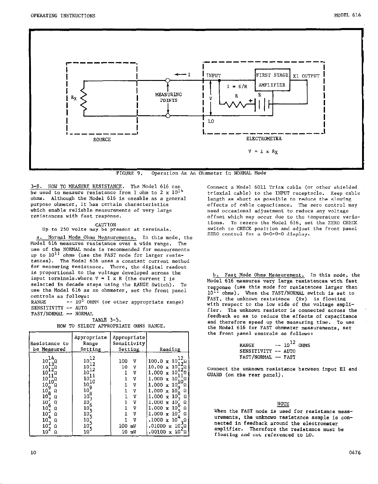
9 Operation as an Ohmmeter in NORMAL Mode
10 Operation as a Coulombmeter in FAST Mode
11
12
13
14
15
16
17
18
19
20
21
22
23
24
25
26
27
28
29
30
31
32
33
34
35
36
37
38
39
Null Method for Current Measurement
Volt-Ammeter
Resistance Method
Unity Gain (Xl) Measuremene
"se of
1V
Recorder Output
Front Panel Of Model 6162
Dual Rack Mounting "sing Model 1007 Hardware
Rear Panel of Model 616 and 6162
Diagram of b,rerconnecrion Cable between 616
Identification of Pins on Digital Output Connector
Suggested Hook-up for Daea Lines
Block Diagram of 61616162 System
Timing Diagram for 6162 Outputs
Overall Block Diagram of Model 616
Simplified Diagram of Amplifier Section
Voltmeter Configuration - NORMAL Mode
Ammeter Configuration - FAST Mode
Coulombmeter Configuration - FAST Mode
Ohmneter Configuration - NORMAL Mode
Functional Black Diagram of *-m-o colwereer 25
Functional Black Diagram of Large Scale Integrated Circuit
DigiLal Display
Chassis Assembly - Exploded View
BOtfOm cover Assembly
Component Layout, PC-321
Gxnpanene Layout, PC-335
Component Layout, PC-322
Component Layout, PC-323
Component Layout, PC-324
Component Layout, PC-325
1
2
3
5
5
7
8
8
10
11
12
12
12
12
13
13
14
and 6162 14
16
18
19
19
21
22
23
23
24
24
26
26
39
39
53
54
55
57
59
60
1175
Page 4
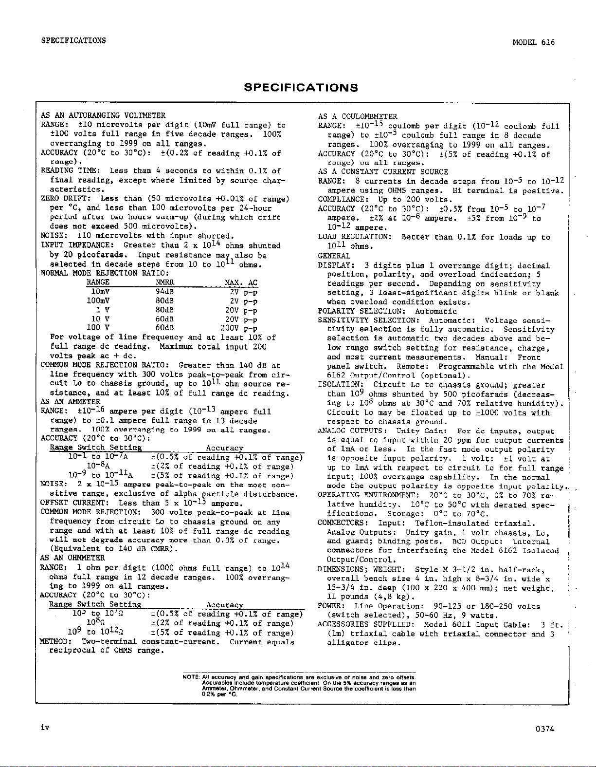
SPECIFICATIONS
MODEL 616
SPECIFICATIONS
iS AN AUTORANGING VOLTMETER
RANGE: $10 microvolts per digit (1OmV full range) eo
Cl00 volts full range in five decade ranges. 100%
overranging to 1999 0" all ranges.
KCUPACY (ZO'=C to 30°C): +(0.2% of reading x).1% of
range).
READING TIME: Less the" 4 seconds to within 0.1% of
final reading, except where limited by source char-
acteristics.
ZERO DRIFT: Less than (50 microvol~s M.Ol% Of range)
per 'C. and less than 100 microvolts per 24-hour
period after two hours warm-up (during which drift
does "a~ exceed 500 microvolts).
IOISE: Cl0 microvolts with input shorted.
tNl'UT IMPEDANCE: Greater than 2 x 10¹⁴ ohms shunted
by 20 picofarads. Input resistance ms also be
selected in decade see"s from 10 ?o
POR”AL MODE REJECTION RATIO:
FQT voltage of line frequency and se least 10% of
full raoge dc reading.
volts peak ac + dc.
:OMMON "ODE RWECTION RATIO: Greater than 140 dB af
line frequency with 300 volts peak-to-peek from circuit Lo to chassis ground, up to 1011 ohm source me-
sistance, and se least 10% of full range dc reading.
is AN AMMETER
?.ANGE:
range) to to.1 ampere full range in 13 decade
ranges. 100% overranging to 1999 on all ranges.
u2cuRAGY (2OY to 30-C):
Range Switch setting AWurecy
YOISE: 2 x lo-15 ampere peak-to-peak on the most sen-
sitive range, exclusive of alpha particle disturbance.
,FFSET C"Rp,XNT:
:OMMON MODE REJECTION: 300 volts peak-to-peak ae line
frequency from circuit La eo chassis ground on any
range and with at least 10% of full range dc reading
will not degrade accuracy more than 0.3% of range.
(Equivalent to 140 dB CMRR).
LS AN OHMMETER
WGE: 1 ohm per digit (1000 ohms full range) co 1014
ohms full range in 12 decade ranges. 100% overranging to 1999 on all ranges.
uxxRAm (2OOC to 3ooc):
Range s;*tci seetinp
IETNOD: Two-terminal COnSt*nr--Curre"t. current equals
reciprocal of OHMS range.
RANGE
1OmV
10omv
1V
10 v
100 v
t10-16 ampere per digit (lo-13 ampere full
10-l Co 10-/A
lo-88
10-9 eo lo-1lA
Less than 5 x lo-15 ampere.
103 to lo’&?
lOan
109 to 10120
NMRR
94dB
80dB
SOdB
60dB
60dB
Maximum total input 200
k(O.54 of reading +O.l% of range)
t(24 of reading +0.1X of range)
CO% Of reading +a.l% Of range)
f(0.54 of reading tO.l% of range)
C(2% of reading +O.l% of range)
+(5% of reading ffl.19. of range)
I1
10
MAX. AC
2v
2v
2ov p-p
2ov 0-p
2oov p-p
Accuracy
ohms.
e-p
p-e
AS A COULOMBMETER
RANGE: ?10-15 coulomb ,,er dinit (LO-12 coulomb full
range) to ?10-5 coulo;b fuli range in a decade
ranges. 100% overranging to 1999 on all ranges.
ACCURACY (20°C to 3O'C): ~(5% of reading +O.l% of
range) 0" a11 ranges.
AS A CONSTANT CURRENT SOURCE
RANGE: 8 CurrentS in decade seeps from 10-5 fo lo-12
ampere using OHMS ranges. Hi eermina1 is positive.
COmJLIANCE: up to 200 volts.
ACCURACY (ZO'C eo 3O'C): 20.5% from 10-5 eo lo-7
ampere. *2% at 10-a ampere. ?5% from 10-9 to
10-12 ampere.
LOAD REGULATION:
1011 ohms.
GENERAL
DISPLAY: 3 digits plus 1 overrange digit; decimal
position, polarity, and overload indicaeio"; 5
readings per second. Depending on sensitiviey
setting, 3 least-si~ificant digits blink or blaok
"he" overload condition exists.
POLARITY SELECTION: Automatic
SENSITIVITY SELECTION: Automatic: Voltage sensi-
tivity selection is fully sutomstic.
selection is a"Wma?Lc hlo decades above and be-
low range switch setting for resistance, charge,
and most current measurements. Manual: Front
panel switch. Remote: Progrsnmsble with the Model
6162 Output/Control (optional).
ISOLATION:
than LO9 ohms shunted by 500 picofarads (decreasing to lOa ohms at 3O'C and 70% relative humidity).
Circuit Lo ma" be floated UD to tlOO0 voles with
respect eo chassis ground.
ANALOG OUTPUTS: Unity Gain: For dc inputs, oueput
is equal to input within 20 ppm far oueput cur;e"rs
Of 1mA or less. In Jhe fasf mode output polarity
is opposite input polarity.
up fo 1mA with respect to circuit Lo for full range
inwt: 100% o"elxs"!Le caoaLli1iev. I" tile normal
mode rhe outpue pol&ity'is oppbsice input polarity
0PEuTING ENVIRONMENT: 20°C eo 3O"C, 0% co 70% re-
lative humiditv. 1O'C fo 5O'C wieh derated soec-
Better than 0.1% for loads up to
sensieiviey
Circuit Lo to chassis ground; greater
1 vo1c: ?l volt at
ifications. s&age: ooc to 70°C.
CONNECTORS:
Analog outputs: Unity gain, 1 volt chassis, Lo.
and guard; binding poses. BCD Output:
co""eceors for interfacing ?he Node1 6162 Isolated
OutpuflConCrol.
DIMENSIONS; WEIGHT: Style M 3-l/2 in. half-rack,
OVer811
15-314 in. deep (100 x 220 x 400 mm); "et weighC,
11 pounds (4,a kg).
POWER:
(switch selected), 50-60 Hz, 9 watts.
ACCESSORIES SUPPLIED: Model 6011 Input Cable: 3 ft.
(lm) rriaxial cable with triaxial co""ector and 3
auigaeor clips.
1npue:
bench size 4 in. high x a-314 in. wide x
Line Operario":
Teflon-insulated trisxial.
1neerna1
go-125 0r 180-250 volts
1
iv
0374
Page 5
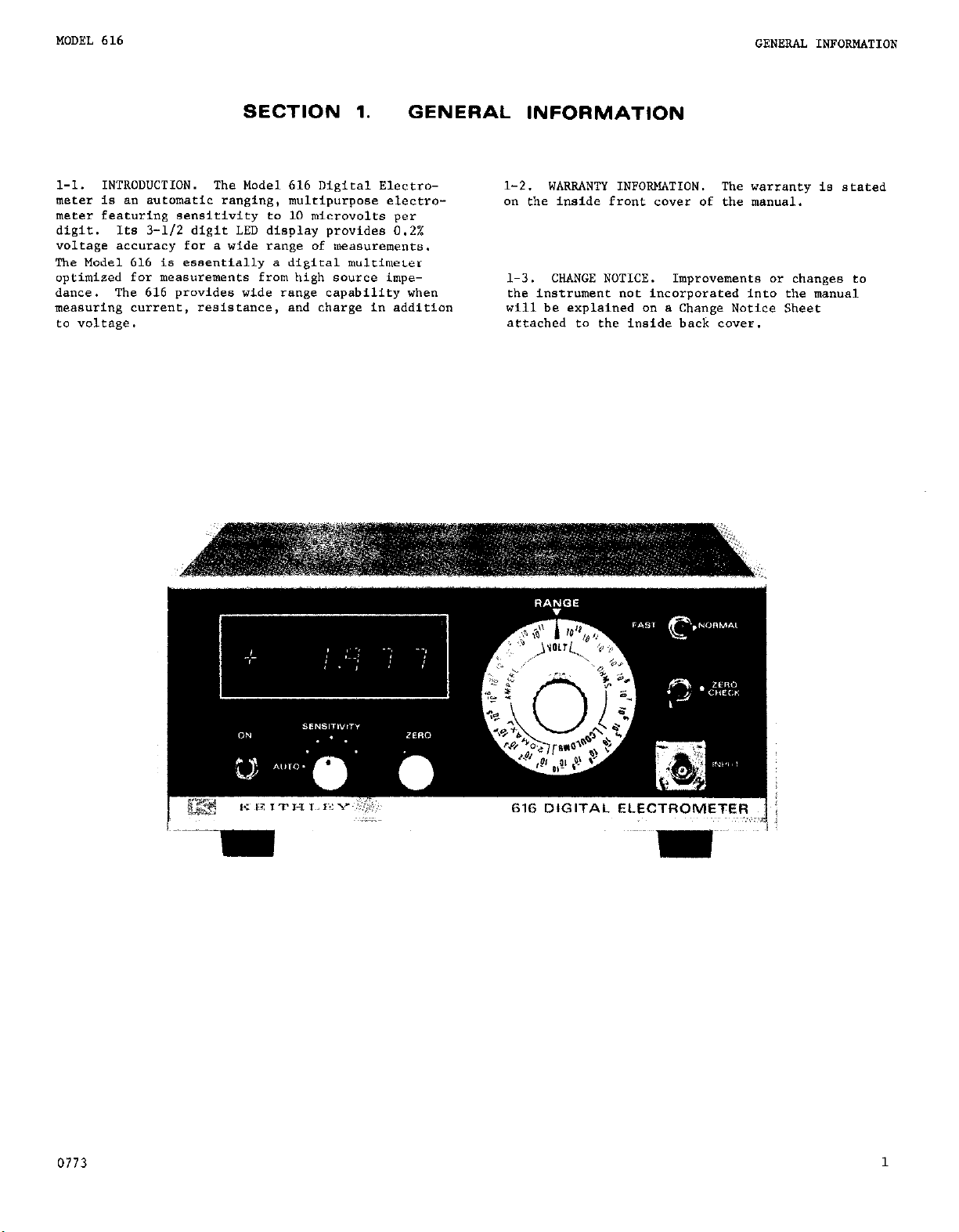
SECTION 1.
GENERAL INFORMATION
l-l. INTRODUCTION. The Model 616 Digital Electrometer is an automatic ranging, multipurpose electrometer featuring sensitivity to 10 microvolts per
digit. Its 3-l/2 digit LED display provides 0.2%
voltage accuracy for a wide range of measuremente.
The Model 616 is essentially a digital multimeter
optimized for measurements from high source impedance. The 616 provides wide range capability when
measuring current, resistance, and charge in addition
to voltage.
1-2. WARRANTY INFORMATION. The warranty is stated
an the inside front cover of the manual.
l-3. CHANGE NOTICE. Improvements or changes to
the instrument not incoqmrated into the manual
will be explained on a Change Notice Sheet
attached to the inside back cover.
0773
1
Page 6
GENERAL INFORMATION
MODEL 616
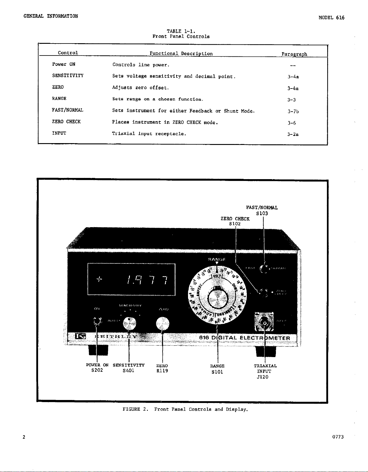
TABLE 1-l.
Front Panel Controls
Control
Power ON
SENSITI"ITY
ZERO
RANGE
FAST/NOW
ZERO CHECK
INPUT
Functional Description
Controls line power.
Sets voltage sensitivity and decimal paint.
Adjusts zero affset.
Sem range on a chosen function.
Sets instrument for either Feedback or Shunt Mode.
Places instrument in ZERO CHECK mode.
Triaxial input receptacle.
FAST/NORMAL
ZERO CHECK
Paragraph
--
3-4a
3-4a
3-3
3-7b
3-6
3-2a
s103
I
POWEk
ON
S202
SENSIiIVITY
s401 R119
FIGURE 2.
RANGE
SlOl
Front Panel Controls and Display.
n&AXIAL
INPUT
5120
0773
Page 7
MODEL 616
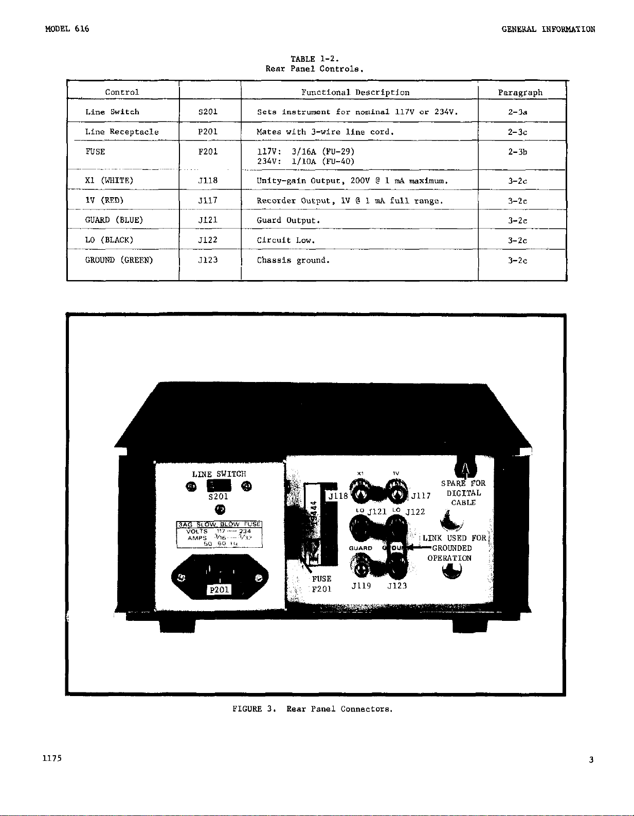
TABLE 1-2.
Rear Panel Controls.
Conrrol
Line Switch
1v (RED) 3117
I
Functional Description
Sets instrxment
Mates with 3-wire
117V: 3/16A (FU-29)
234V: l/lOA (FU-40)
Unity-gain ouqmt, zoov @ 1 lnA maximum.
Recorder Output, 1" @ 1 mA full range.
Guard Output.
circuit LOW.
Chassis ground.
for nominal
line
cord.
117V or 234V.
Paragraph
2-3a
2-3~
2-3b
3-2c
3-2c
3-2~
3-2c
3-2~
-
-
1175
FIGURE 3. Rear Panel Connecears.
3
Page 8
INITIAL PREPARATION MODEL 616
SECTION 2. INITIAL PREPARATION
Z-l. GENERAL. This section describes procedures far
incoming inspection and preparation for use.
2-2.
INSPECTION.
The Model 616 was carefully inspected both mechanically and electrically before
shipment.
Upon receiving the instrument,
check
for any obvious damage which may have occurred during transit.
Report any damages to the shipping
agent.
PREPARATION FOR USE.
2-3.
8. Line Voltage.
Before power is applied check
the position of the LINE switch (5201) on the rear
panel.
50-60
Select the 117V position for operation from
Hz line voltages over the range 9OV to 125"
rms . Select the 234V position for operation fro,,,
50-60
Hz line voltages over the range 1SOV to 250"
rms . Line voltages which are not cavered by ranges
specified require an appropriate step-up or stepdawn pawer transformer.
b. Fuse Installation.
After the line "alrage
range is selected check for the proper fuse type
and rating 8% fallows:
117v:
234V:
c. Line Co""ectio"s.
3116 ampere, type 3AG
SLO-BLO (FU-29)
l/l0 ampere, type 3AG SLO-BLO (F"-40)
This instrument requires *
three-wire line cord (Keiehley part no. CO-7) which
provides connections t" line voltage (high, common)
and chassis ground.
For operator safety, the
chassis ground pin should be connected to earth
ground.
CZ
If the instzxment input LO is to be floated,
above chassis ground, make certain that the
"link" between LO and GROUND on the rear
panel is removed.
d. Warm-up. The recommended warmup time far the
Model 616 is two hours, although if is useable immediately after power is turned on, for less critical
meas"reme"ts.
4
1175
Page 9
MODEL 616
I
OPERATING INSTRUCTIONS
SECTION 3.
3-1. GENERAL. This section describes the procedures
for operating the Model 616 for measurement of valr-
age, ~uccent, charge, and resistance.
3-2.
HO" TO MAKE INPUT AND OUTPUT CONNECTIONS.
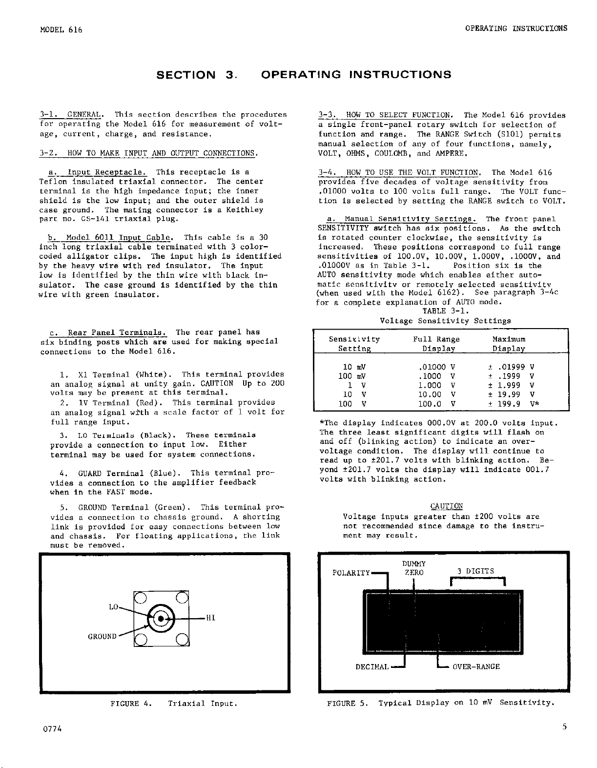
a. Incut Receotacle. This receptacle is a
Teflon insulated triaxial connector. The center
terminal is the high impedance input; rhe inner
shield is the law inout: and the outer shield ie
case ground. The m&n; connector is a Keirhley
part "0. CS-141 triaxia1 plug.
b. Model 6011 Input Cable. This cable is a 30
inch long triaxial cable terminated with 3 colorcoded alligator clips. The input high is identified
by the heavy wire with red insulator. The input
low is identified by the thin wire with black in-
sulator. The case ground is identified by the thin
wire with green insulator.
C. Rear Panel Terminals. The rear panel has
six binding posts which are used for making special
connections to the Model 616.
1. Xl Terminal (White). This terminal provides
an analo,q signal at unity gain. CAUTION Up to 200
volts my be present at this terminal.
2. 1" Terminal (Red).
an analog signal wivh a scale factor of 1 volt far
full range input.
3.
Lo Terminals (Black). These terminals
provide a connection to input low.
terminal may be used for system connections.
GUARD
4.
vides a connection to the amplifier feedback
when in the FAST made.
5. GROUND Terminal (Green).
vides a connection to chassis ground. A shorting
link is provided for easy connections between lo"
and chassis. For floating applications, the link
must be removed.
Terminal (Blue). This terminal pro-
This terminal provides
Either
This terminal pro-
OPERATING INSTRUCTIONS
3-3.
HOW TO SELECT FUNCTION.
a sinele front-"anel rotarv switch for selection of
function and range.
manual selection of any of four functions, namely,
VOLT, OHMS, COULOMB, and AMPERE.
3-4.
HOW TO "SE THE, VOLT FUNCTION.
provides five decades of voltage sensitivity from
.OlOOO volts to 100 volts full range. The VOLT func-
tion is selected by setting the RANGE switch to VOLT.
a. Manual Sensifivity Setfin~s. The front panel
SENSITIVITY switch has six positions. ks the switch
is rotated counter clockwise, the sensitivity is
increased.
sensitivities of lOO.OV, lO.OOV, l.OOOV, .lOOOV, and
.OlOOOV as in Table 3-1.
AUTO sensitiviry mode which enables either *"tomatic sensitivitv or remotely selected sensitivitv
(when used with the Model 6162). See paragraph 3-4~
for a complete explanation of
Senslriviey
Setting
I
I
10 nlv
100 nlv
10 1v v
100
*The display indicates OOO.OV at 200.0 volra input.
The three least significant digits will flash on
and off (blinking action) to indicate an over-
voltage condition.
read up to f201.7 volts with blinking action. Beyond f201.7 "olts the display will indicate 001.7
volts with blinking action.
Valtaae inputs ,q.reater than f200 volts are
not r;comm&,ded-since damage to the instrument may result.
These positions correspond to full range
Voltage Sensitivity Settings
" 100.0 199.9 v*
The RANGE Switch (5101) permits
TABLE 3-1.
Full Range Maximum
Display Display
.01000 v
.lOOO v f .1999 v
1.000 10.00 v V v f i f 1.999 19.99 v v
The display will continue to
The Model 616 provides
The Model 616
Position six is
AUTO
mode.
f .01999 v
the
0774
GROUND
FIGURE 4. Triaxial Input.
POLARITY ZERO
DUMMY
1, -
DECIMAL--I
FIGURE 5.
Typical Display on 10 mv Sensitivity.
3 DIGITS
LOVER-RANGE
5
Page 10
OPERATING INSTRUCTIONS MODEL 616
b. Automatic Sensitivity Operation. In the AUTO
mode, the Model 616 automatically selects the proper sensitivity in accordance with the following
rules.
1. Upranging. If the display reading is between O-l-S-0 and l-9-9-9 and the i""ut siwal
is increased beyond l-9-9-9, the Model 616 auto-
matically up-ranges to the next higher (less
sensitive) range.
The three least significant
digits sre blanked during range changing so ss
to prohibit incarrect readings from being dis-
played.
If the input signal exceeds t199.9 volts
the display will continue to indicate up to f201.7
volts but the three least significant digits will
flash on and off to indicate an over voltage
condition.
2. Down ranging. If the display reading is
~-
at least O-I-S-O and the input signal is decreased,
the Model 616 automatically down ranges to the next
lower (mare sensitive) range.
C. Remote Sensitivity Selection. When the Model
616 is used with the Model 6162 Isolaced 0uc"utl
.
Control, the 616's voltage sensitivity may be cemerely selected.
The output connector on the rear
panel of the 6162 provides four isolated control
lines for the purpase of remote sensitivity progr*""i.*g.
3-2.
The lines are coded as shown in Table
The 616's front panel SENSITIVITY switch
must be set t" AUTO position.
TABLE
3-2.
Remote sensitivity Programmi"g Logic
Sensitivity
Control Lines
&CR*
K4
R2
Kl
I
.01000 "
.lOOO v
1.000
10.00
100.0
I: ", : :
” 1 0
v : 1 1 0'
" 0 1 1 1
*NOTE
The Manual Range line MR is used to defeat
the automatic sensitivity feature. When MR
is open, the 616 returns to s"tomatic operatian. Logic 1 - open, Iogic 0 = closure to
ground.
3-5.
PO" TO SELECT RANGE ON OHMS, COULOMB, AND AMPERE.
The front panel KANGE switch (SlOl) provides selection
of four functions, VOLT, OHMS, COULOMB, and AMPERE as
described in paragraph 3-3. For each function, a wide
selection of ranges is provided; 8 ranges on
OHMS,
4
ranges "n COULOMB, and 11 ranges on AMPERE. Since
the SENSITIVITY switch is used in conjunction with
the RANGE Switch, the actual number of usesble spans
is 12 decades on OHMS, 8 decades an COULOMB, and 11
on AMPERE.
NOTE (ON AMPERE FUNCTIONl
On the 10qlA t" 10~4A ranges, the voltage beveloped must not exceed 2 volts, otherwise,
overheating of s range resistor could result.
As s result,
the
10 Volt and 100 volt sensitivity settings ate not recommended for lo-l1\
to
1O-4A ranges.
TO interpret a reading an OHMS, COULOMB, or AMPERE
ranges both the digital display (with decimal location)
snd the RANGE setti"g(powers of ten)shauld be cansidered.
For example, given a digital reading of 17.32
and a RANGE setting of 1O-7 AMPERE, the actual measured value would be interpreted ss 17.32 x lO-7
ampere.
Since the decimal point is moveable, it is important
to notice the position of the demimal point to determine the full range of the instrument. See Table 3-3
for typical range settings in the AMPERE function.
TABLE
3-3.
Typical Current Range Settings*
Input Range Se"Siti"ity Digital
current setting setting Display
*The current reading is interpreted by multiplying the
display reading times the range setting. Other cucrents not show" can be measured by selecting the
sppr"priste RANGE switch setting in decade steps from
lo-1'A to lo-lA.
3-6.
HOW TO MEASURE VOLTAGE. The Model 616 can be
used to measure voltages from ilO microvolts to i200
volts.
Although the Model 616 is useable as a gener-
al purpose digital voltmeter, it has certain charac-
teristics which enable reliable meas"rement~ from
very-high source resistsnces. When used in the VOLT
mods, the M el 616 has B" input resistance greater
than 2 x 10%.
As a result, the loading of the
source circuitry is relatively insignificant when
compared to typical digital voltme-cers having LOS
ohms input resistance. The Model 616 has 20 picofarads of shunt capacitance (not including the input
cable capacitance),
since a large *"o""t Of capaci-
tance causes a slowing of response, the input capaci-
ty ,shauld be kept 8s small as possible.
a. Measurements From Very High Source Resistance.
TO "se the Model 616 as a voltmeter, set the front
pane1 controls as follows:
RANGE
-- VOLT
SENSITIVITY -- AUTO
FAST/NORMAL -- NOW
Connect a Model 6011 Triax Cable (or other shielded
triaxial cable) to the INPUT receptacle. Keep cable
length as short as possible to reduce the slowing
effects of cable capacitance. The ser" control may
need occasional adjustment to reduce any voltage
offset which msy occur due to temperature variations.
To
resero the Model 616, set the ZERO CHECK switch
to CHECK position and adjust the front panel ZERO
control for a O-O-O-O display.
The Model 616 pravides a direct reading voltage display with automatic
decimal point position and polarity.
6
0476
Page 11
OPERATING INSTRUCTIONS
I
---------_
SOURCE
b. Measurements From Low source Resist.a”ce. TO
"se the Model 616 for voltage measurements from low
~our'ce resistances, set the RANGE switch to the lo-l1
AMPERE position. In this mode, the Model
resistance is reduced to 1011 ohms; as a result the
electrometer will be lees sensitive to electrical
noise pickup and input cable vibration. Voltage
measurements can be made by following the same
procedure given in paragraph 3-6a. The Model 616
can be used with the RANGE eet et any position be-
tween 10-11 AMPERE to 10-l AMPERE.
input resisLence can be determined by taking the
reciprocal of the AMPERE setting. Significant loading error may result if the input reeisrsnce 18
reduced to less than 100x the source resistance.
C. Measuremenrs Above 200 Volts. The Model 616
can be used with accessory divider probes to measure
voltages up to 30 kilovolts. Range muse be set to VOLT.
1. Model 6102A Divider Probe (1O:l). This
accessory extends the voltage mesauring capability
of the Model 616 to 1000 volts. The inpa resistance is lOlo ohms.
to 1000 volts.
ory Model 6012 Adapter is needed LO mete the triaxial input with the UHF connector a" the probe.)
2. Model 6601A Divider (1OO:l). This accessory
extends the voltage measuring capability of the
Model 616 to 5000 volts. The input resistance is
lo7 ohms. The divider accuracy ia +0.01X.
3. Model 6103A Divider Probe (1OOO:l). This
accessory extends the voltage measuring capability
of the Model 616 to 30 kilovolts. The input resistance is 10"
f5% to 30 kilovolta.
an accessory Model 6012 Adapter ie needed to mate
the triaxial input with the "HP connector on the
probe.)
The divider accuracy is +4%
(To use the Model 6102A en acceee-
ohma.
The divider accuracy is
(To
uee the Model 6103A
i
ERROR DUE TO CIRCUIT LOADING
% ERROR =
616 input
The Model 616
100 R
R + RIN
-----------------’
I
ELECTI(OMETER
The Model 616 may exhibit a large amount of
zero offset or drift immediately after an
overload or e long period of storage. I"
addition, the offset current may exceed the
specification for a short time until the
Model 616 ia sufficiently stabilized.
Although the offset current of the Model 616
is well below offset found in conventional
voltmeters, the effects of the offset current
charging the input capscitance may be "ociced
when the input is open. "se the ZERO CHECK
switch to discharge the offset charge.
The Model 616 should "ot be operated with circuit low fleeting by greater than 1000 volta
with respect to chassis ground.
616 is to be used with circuit low floating
make certain that no connection is made be-
tween the LOW and GROUND terminals o" the
rear panel.
corder or other instrument to the Xl or 1V
outpute when the Model 616 is floated.
d. Voltage Measurements in FAST Mode. when the
FAST/NORMAL Switch is eet to FAST, the Model 616 is
connected in a "FEEDBACK" amplifier configuration.
In this configuration, the Model 616 requires special
connectians.
between input HI and GUARD. A" easy way to accomplish this connection ie Lo connect the link (on the
rear panel) between "GUARD" (blue terminal) and
"GROUND" (green terminal). Then uee the rriaxial
cable far input connectione with the input voltage
applied between the "red" clip lead and the "green"
clip lead.
In this special voltage connection, the LO
input (black clip lead) is "of used since
the voltage amplifier Configuration has bee"
changed.
Do not connect a grounded re-
To measure voltage, co~ect the eource
NOTE
If the Model
1175
7
Page 12
OPERATING INSTRUCTIONS
c------c--
c------c--
l l
R R
I I
II--, II--,
I I
------F----------
------F----------
l
l
MODEL 616
I I
MEASURING MXASURING
POINTS POINTS
I I
I I
- -
i i
T T
: :
--WC---- --WC----
L L
; ;
I I
_I’ _I’
SOURCE SOURCE
P1G"P.E 7. PICURE 7.
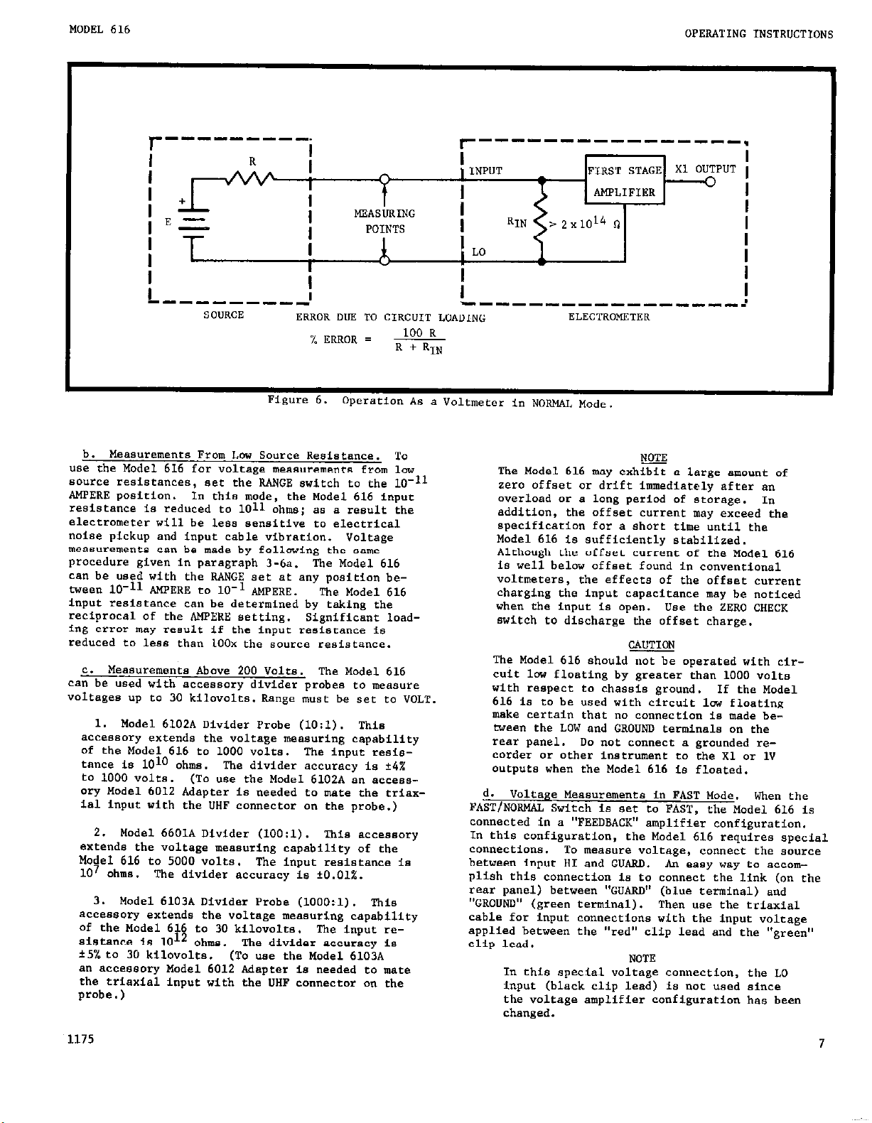
HOW To MEASURE CURRENT. The Model 616 can be
3-7.
wed to measure currents from *lo-15 ampere to 200
mill***peres.
a general purpose picoammerer, it has certain charac-
teristics which enable reliable measurements of very
small current8 with fast response.
a. Normal Mode Current
mode for current below lo-5A.) I" this mode, the
Model 616 measures current "ver a wide range. When
the FAST/NORMAL switch is set to NORMAL, the Model
616 operates as a shunt-type picaammeter in which a
resistor is connected directly across the input terminals.
acro.m the shunt resistors where VIN - IIN x RS.
This method of measurement is typical of 'mast multimeter current measuring techniques. To use the Model
616 as a shunt-type pidoammeter, eat the front panel
controls *s fallows:
RANGE
SENSITIVITY -- AUTO
PAST/NORMAL -- NORMAL
Full range is determined by the
sensitivity setting and the AMPERE
range setting.
Connect a Model 6011 Triax Cable (or other shielded
eriaxial cable) to the INPUT receptacle. Keep cable
length as short as possible to reduce the slowing
effects of cable capacitance. The zero control may
need occasional adjustment to reduce any voltage
offset which may occur due to temperature variations.
To rezer" the Model 616, set the ZERO CHECK switch
to CHECK position and adjust the front panel Zero
control for a O-O-O-O display.
Although the Model 616 is useable a8
Measurements.
The Model 616 measures the voltage drop
-- 10-5
AMPERE (or appropriate range)
NOTE
-
operation As A" hater in NORMAL Mode. operation As A" hater in NORMAL Mode.
(Use FAST
L1-__------------! L1-__------------!
ELECTROMETER ELECTROMETER
” = I x Rm ” = I x Rm
The Model 616 may exhibit a large em"u"t of
zero offset or drift immediately after a"
overload or a long period of storage. I"
addition, the offset current may exceed the
specification far a short time until the
Model 616 is sufficiently stabilized. Al-
though the offset current of the Model 616
is well below offset found in conventional
voltmeters, the effects of the offset current
charging the input capacitance may be noticed
when the input is open. Use the ZERO CHECK
switch to discharge the offset charge.
Do not use the 10 volt and 100 volt aensi-
tivity settings for RANG? switch settings
of LO-~, 10e2, 10v3, and 10e4 ampere.
the voltage ekeeds~2 volts on these ranges,
averheating of the resistors could result
with subsequent degradation of accuracy in
the AMPERE mode.
If
0476
Page 13
MODEL 616
OPERATING INSTRUCTIONS
b. Fast Mode C rrent Measurements.
currents from 10 A and smeller.) In this mode, the
-s
(Useable for
Model 616 measures very amall currents with fas;
response. When the FAST/NORMAL switch is set to
FAST, the Model 616 operates as a feedback-type
picaammeter in which the current flows through the
feedback resistor of the voltage amplifier. The
Model 616 indicates the voltage developed across
the range resistor where VF =
method of measurement provides
I
Es: ~~p0~8*since
the effect of the input capacitance from lengthy
cables is diminished.
To use the Model 616 as a
feedback-type picoammerer, set the front panel
controls *s follows:
RANGE
-- lo-l1 AMPERE
SENSITIVITY -- AUTO
FAST/NORMAL -- FAST
Connect a Model 6011 Triax cable (or other shielded
triaxial cable) to the INPUT receptacle.
The zero
control may need occasional adjustment to reduce any
voltage offset which may occur due to temperature
"S.***t*O~S.
To rezero the Model 616, set the ZERO
CHECK switch to CHECK position and adjust the front
panel ZERO control for a O-O-O-O display.
The Model 616 may exhibit a large amount of
zero offset or drift immediately after an
overload or a long period of storage. In
addition, the offset current may exceed the
specificarion far a short time until the
Model 616 is sufficiently stabilized. Al-
though the offset current of the Model 616
is well below offset found in conventional
voltmeters, the effects of the offset current
charging the input capacitance may be hoticed
when the input is open. Use the ZERO CHECK
switch to discharge the offset charge.
2) Considerafions~When
Measuring
C&rent. When
using the Model 616 in either the NORMAL or FAST
nodes, there are certain considerations which ensure
optimum performance.
In general, it is advantageous
to use the smallest possible value of shunt resis-
tance for a picoammeter.
Fir*t, small value resistors are of higher quality compared to large values
with respect to accuracy, time stability, temperature. and voltage coefficient, Second, ideal picoammeters require very small input resistance so that
source loading does not affect the overall accuracy
of the measurement.
Since the input resistance
in a shunt picoammeter is determined by the range
resistor, the RANGE multiplier should be set at the
lowest value.
Third, the use of a low value resis-
tor reduces the input RC time constant and results
ln faster response.
Harever, since noise and zero
irift become more significant when the voltage
unplifier sensitivity is set to 10 or 100 millivolts,
the appropriate range multiplier should be selected
with a one volt full scale sensitivity. The use of
the Model 616 in the FAST made enables measurements
of very small currents while reducing the source
loading and input RC time constant. Since the range
resistor is connected in the feedback of the voltage amplifier, the effective input resistance is
determined by the open-loop gain where SIN = RF t A.
(The value of A is typically 10,000.) Another advantage of the feedback mode is the reduced effect
of input capacitance since the input SC time copstant is decreased by the gain A (RCeFpECTIVE = RC i
As a result, the measurement speed is governed
A).
by the feedback time constant which is a function
of the feedback resistor and stray capacitance acT088
the resistor (usually a few pF). Thus, when comparing shunt versus feedback modes, it is evident that
the feedback measurement offers superior performance
for most applications.
TABLE 3-4.
HOW TO SELECT APPROPRIATE AMPERES RANGE.
urrent To
a Measured
lo-15A
10-14A
lO:;;A
10 A
;;I:~
Range
Setting
10-11
g:::
10-11
$"
LO-' A
,ppropriate
LO-' A
lO-7 A
10-6 A
1O-5 A
10-e
10-7
lo-6
10-5
1O-4 A 10-4
lO-3
A
10-3
1O-2 A 10-2
10-l A
10-l
Appropriate
Sensitivity
Setting
10 In"
10 In"
10 mv
100 mv
1"
1v
1v
1"
1v
1v
1v
1v
1v
1v
1v
NOTE
-
.OOOlO x lo-1lA
.OOlOO x 10-llA
:;;;p,xl;";:';
;:g; : ;$ ;
1.000 x lo-' A
1.000 x lO-8 A
1.000 x lO-7 A
1.000 x
lo-6
1.000 x 10-S A
1.000 x 10⁻⁴ A
1.000 x 1O-3 A
1.000 x 1O-2
1.000 x 10-l A
The we of the FAST mode for current measurements
is subject to certain restrictions ae follars:
1. The range resistor value should not be
greater than the source resistance, otherwise
feedback division results in zero instability at
the output.
2. The largest value of current measured
should not exceed 10e5 ampere, otherwise the
full feedback current cannot be developed.
The NORMAL mode should be used for currents
from 200 mA to 10-4A.
A
A
3476
9
Page 14
OPERATING INSTRUCTIONS
MODEL 616
r---------m
-1
I
I
MEASURING
I %
I ..----,---,I
SOURCE
FIGURE 9.
3-8. HOW TO MEASURE RESISTANCE.
be used to measure resistance from 1 ohm to 2 x 10¹⁴
ohms. Although the Model 616 is useable as a general
purpose ohmeter, it has certain characteristics
which enable reliable measurements of very large
resiseances with fast response.
Up to 250 volts may be present at cerminale.
a. Normal Mode Ohms Measurements.
Model 616 measures resistance over a wide range. The
use of the NORMAL mode is recommended for measurements
up to 1O'l ohms (use the FAST mode for larger resis-
tallces). The Model 616 uses a constant current method
for measuring resistance.
16 proportional to the voltage developed across the
input terminals.where V = I x R (the current I is
selected in decade steps using the RANGE Switch). To
use the Model 616 as an ohmmeter, sac the front panel
controls 88 follows:
RANGE
SENSITIVITY -- AUTO
FAST/NORMAL -- NORMAL
e***t**ce to
be Measured
lOl$
1012n
IOllQ
$0;
109 0
108 n
10' n
106 n
lo5 n
104 n
103 n
lo2 n
-- 105 OHMS (or other appropriate range)
HO" TO SELECT APPROPRIATE ONMS RANGE.
Lppropriate
14
CAUTION
There, the digital readout
TABLE 3-5.
Range
Setting
;;::
1012
1011
1010
109
108
107
106
lo5
105
105
105
The
1v 1.000 x loL"n
1 "
1 v 11.000
1v 1.000 x 10' n
1v 1.000 x 10⁶ n
1v 1.000 x 10⁵ n
1 " .I""" x n 104
Operation As An Obrmneter in NORMAL Made
Model 616 can
In this mode, the
1.000 x log n
x 10: n
x 1030
x 1o‘al
.--------------m-w.
INPUT
L---,--- ------ --,I
ELECTROMETER
" = I x Rx
Connect a Model 6011 Triax cable (or other shielded
triaxial cable) to the INPUT recept&le. Keep cable
length as short as possible to reduce,the slowing
effects of cable capacitance. The zero control may
need occasional adjustment to reduce any voleage
offset which may occur due to the temperature "aria-
thl*.
switch t-0 CHECK position and adJust the front panel
ZERO control for a O-O-O-O display.
Model 616 meaeures very large resistancea with fast
y$a
FAST, the unknown resistance (Rx) is floating
with respect to the low side of the voltage ampli-
fier.
feedback so as to reduce the effects of capacitance
and therefore speed up the measuring time. TO use
the Model 616 for FAST ohmmeter measurements, see
the front panel controls as follows:
Connect the unknown resistance between input HI and
GUARD (on the rear panel).
I
To rezero the Model 616, set the ZERO CHECK
b. Fast Mode Ohms Measurement. In this mode, the
onse (use this mode for resistances larger than
ohms). When the FAST/NORMAL switch is set to
The unknown resistor is connected across the
RANGE -- 1012 OHMS
SENSITIVITY -- AUTO
FAST/NORMAL -- FAST
When the FAST mode is used for resistance measurements, the unknown resistance sample is connected in feedback around the electrometer
amplifier.
floating and not referenced to LO.
Therefore the resistance must be
I
10 0476
Page 15
r---------1
I
CHARGE
TRANSFER--t,
I I
n
,m----------- -----,
, INPUT
I
I +
' %/
I
I
b---m-----?
3-v. HOW TO MEASURE CHARGE. The Model 616 can be
SOURCE
I
I
I
I
MEASURING
POINTS
&
used LO measure charge by means of a current integration technique.
anyone of the 4 coulomb ranges, an accurately known
"hen the Model 616 is set to
capacitor is connected in the feedback loop of the
voltage amplifier so chat the voltage developed is
~oportional to the integral of current where V =
'C or V = l/Ciidt. To use the Model 616 as a coul-
ombmeter, 8et the front panel controls as follows:
RANGE -- 10-10 COULOMB
SENSITIVITY -- AUTO
FAST/NORMAL -- PAST
Connect a Model 6011 Triax cable ("r other shielded
Lriaxial cable) to the
INPUT
receptacle. Keep cable
length a8 short as possible to reduce the slowing
effects of cable capacitance. The zero control may
need occasional adjustment to reduce any voltage
offset which may occur due to the temperature variatiO"S. To rezer" the Model 616, set rhe ZERO CHECK
Switch t" CHECK position and adjust the front panel
ZERO control for a O-O-O-O display.
NOTE
-
The input offset current of the Model 616
contributes a charge of 5 x lo-15 coulomb
per second and should be subtracted- from
the actual reading.
The Model 616 can also be used with acces-
sory Models 2501 or 2503 for measurement af
static
charge 0" a dielectric surface.
A
discussion of static charge measurement is
given in secrion 3-lla.
For m"re information about Static Charge
Measurements, request the Keichley PrOduct
Notes entitled "Electrometer Static Charge
Measurements”.
i
,Lc
I
.-.------------____,
3-10.
HOW TO "SE AS A CURRENT SOURCE. The Model 616
ELECTROMETER
v = l/C /i dt
I
can be used as a current .s"urce for currents in decade increments from 10-5A t" lo-12A. TO select cur-
rent, set Model 616 to OHMS function. set OHMS range
to the appropriate position as show" in Table 3-6.
"se NORMAL mode for currents up to lo-loA, and FAST
made above lo-loA.
TABLE 3-6.
' Current Desired
lo-=A
lo-"A
10-lOA
lo-' A
10-S A
1O-7 A
1O-6 A
lo+ A
OHMS Range
12
1011n
$10;
IO9 n
1oS n
107 R
106 n
lo5 R
When input to Model 616 is not connected,
set Zero Check Switch t" CHECK. If no inp"f connection is made a large voltage
(up to ZOOV)
can appear across the input.
3-11. ALTERNATE MEASUREMENTS. The Model 616 can
also be used with Keithley accessories which ex-
tend the measuring capabilities of the electrometer.
Static Charge Measwement~. The Model 616
a.
can be used with Models 2501 or 2503 Static Detector
Probes far measurement of static charge on a dielectric surface. When using this method, the Model 616
is operated as a voltmeter with a reading directly
in volts.
(Do not attempt t" measure static charge
with the Model 616 in the COULOMB mode.)
1476
11
Page 16
OPERATING INSTRUCTIONS
7’
L,
MODEL 616
I-
1
FIGURE 11.
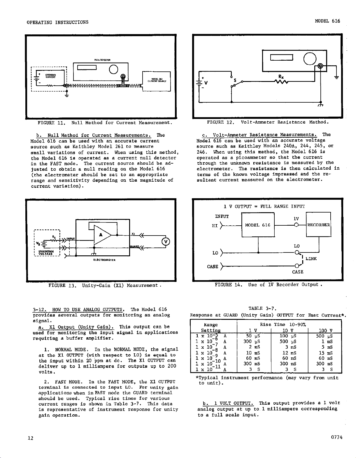
b. Null Method for Current Measurements. The
Model 616 can be used with a" accurate current
source such as Keithley Model 261 t" measure
small variations of current. When using this method,
the Model 616 is operated BB a current null detector
in the FAST mode.
justed to obtain a null reading "n the Model 616
(the electrometer shauld be set t" a" appropriate
range and sensitivity depending on the magnitude of
current variation).
Null Method far Current Measurement.
The current source should be ad-
I
C. volt-Ameter Resistance Measurements. The
Model 616 can be used with a" accurate voltage
source such as Keithley Models 240A, 244, 245, or
246. When using this method, the Model 616 is
operated as a picaammeter so that the current
through the unknown resistance is measured by the
electrometer.
terms of the knaun voltage impressed and the resultant current measured "n the electrometer.
Volt-Ammeter Resistance Method.
The resistance is then calculated iz
1 " OUTPUT = FULL RANGE INPUT
LO +--l--sJ
i LINK
CASE VC;;SE
FIGURE 14.
"se of 1V Recorder Output.
1
3-12.
provides several outputs far monitoring a" analog
signal.
used for monitorina the input sinnal in applications
requiring a buffer-amplifi&. -
12
HO" TO "SE ANALOG OUTPUTS. The Model 616
a. Xl Output (Unity Gain). This ""tput can be
1. NORMAL MODE.
at the Xl OUTPUT (with respect to LO) is equal to
the input within 20 bpm at dc. The Xl OUTPUT can
deliver up tcJ 1 milliampere for Outputs up to 200
volts.
2. FAST MODE.
terminal is connected t" input LO.
applications when inFAST mode the GUARD terminal
should be used.
current ranges is show" in Table 3-7. This data
*a representative of instrument respanse for unity
gain operation.
In the NORMAL MODE, the signal
In the FAST MODE, the X1 OUTPUT
For unity gain
Typical rise times for various
TABLE 3-7.
:sponse at GUA
Range
setting
.- .
*'ryplcal 1*strume*t perrormance <may vary tr"m unit
to unit).
b. 1 VOLT OUTPUT.
analog Output at up to,1 milliampere corresponding
to * full scale input.
RD (Unity Cain) OUTPUT for Fast Curre"
Rise Time
This "utput pravides a 1 volt
lo-90%
0774
Page 17
MODEL 616 OPERATING INSTRUCTIONS
3-13.
provides isolated BCD outputs, remote controls, and
remate pragramming lines for systems we of the Model
616.
farmatian provided in parallel format. Strobe lines
permit data transfer in 4 bit multiples which are
compatible with 8, 12, or 16-bit data eyeterns.
Strobing of the “open collector” wtpute also permit
multiplexing of data from 2 or more 6162’8 an e
single data bus.
l/5 second to 7 seconds per reading to permit a wanefer rate compatible with the speed of measurement
end/or the acquigition system.
trole are provided for Zero Check, Sensitivity, Dfsplay Hold, Output Hold, ae well ae Strobe. The 616’s
low to chessis ground ie018tion is maintained by the
6162 (greater than lolo ohms). Digital w&put lcw
is also isolated from chassis ,ground by 10 ahme.
a separate 3-l/2 in. high half-rack chassis.
be used on the bench adjacent to the 616 or reck
mounted side-by-side in a standard 19 inch rack width
using rack hardware provided (Model 1007).
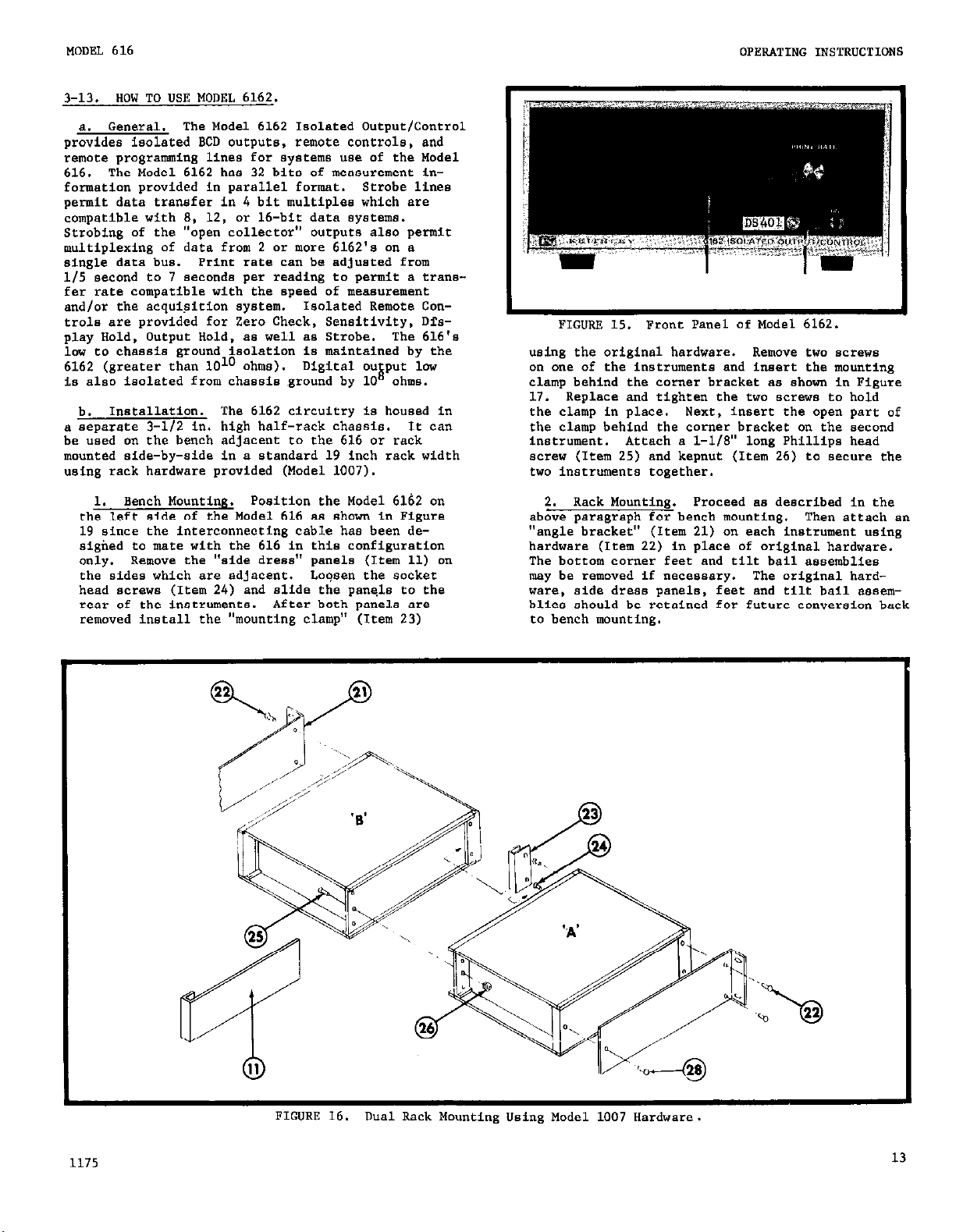
HOW TO USE MODEL 6162.
8. General.
The Made1 6162 has 32 bite of meaeurement in-
Installation.
b.
Bench Mounting. Position the Model 6162 on
1.
the left side of the Model 616 as shown in Figure
19 since the intercanneoring cable has been desighed to mate with the 616 in this configuration
only.
the sides which are adjacent. Loqeen the socket
head screw (Item 24) and elide the panqle to the
rear of the instruments. After both panels are
remaved install the “mounting clamp” (Item 23)
Remove the “side dress” panels (Item 11) on
The Model 6162 Isolated Output/Control
Print rate can be adjusted from
Isolated Remote Con-
The 6162 circuitry is housed in
*e can
FIGURE 15.
using the original hardware. Remove two ecrewe
on one of the instruments and insert the mounting
clamp behind the corner bracket ae shown in Figure
17. Replace and tighten the two ecrewe to hold
the clamp in place.
the clamp behind the corner bracket on the second
i*stTXlE*t. Attach a l-l/L?” long Phillips head
ecrew (Item 25) and kepnut (Item 26) to secure the
two instruments together.
2. Rack Mounting. Proceed 88 described in the
above paragraph for bench mounting. The,, attach a,,
“angle bracket” (Item 21) on each instrument using
hardware (Item 22) in place of original hardware.
The battam corner feet and tilt bail assemblies
may be removed if necessary. The original hardware, side dress panels, feet and tilt bail aeeemblies should be retained for future conversion back
to bench mounting.
Front Panel af Model 6162.
Next, insert the open part of
FIGURE 16.
Dual Rack Mwnting Ueing Model 1007 Hardwarr.
Page 18
OPERATING INSTRUCTIONS
MODEL f
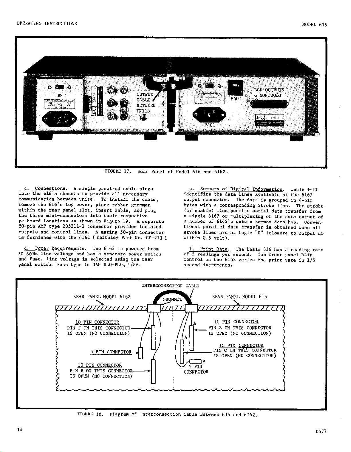
c. Connections.
FIGURE 17.
A single prewired cable plugs
Rear Panel of Model 616 and 6162.
e.
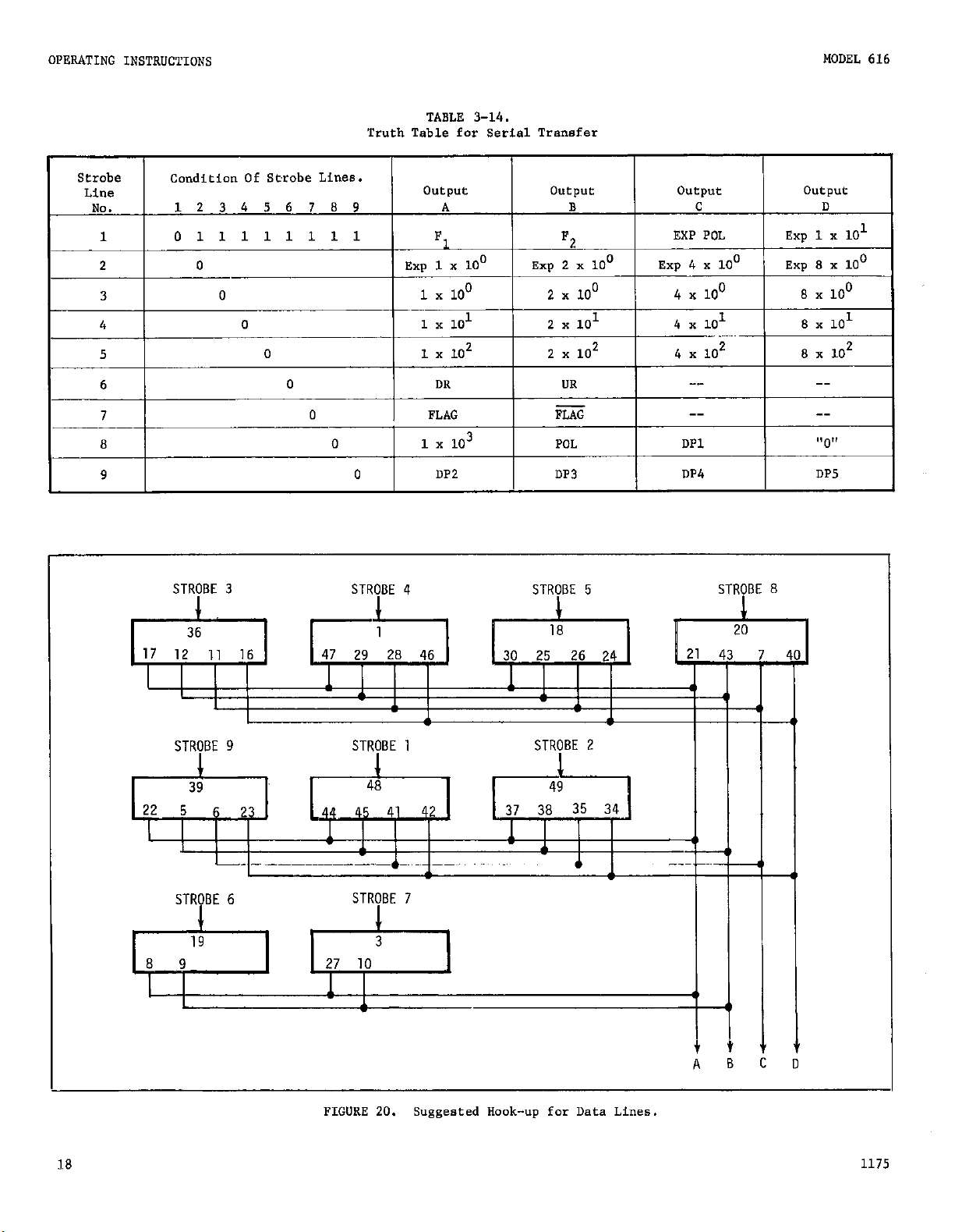
Summary of Digital Information. Table 3-10
into the 616's chassis to provide all necessary identifies the data lines available et the 6162
communication between units. To install the cable,
remove the 616's top cover, place rubber grommet
output connector.
The data ia grouped in 4-bit
bytes with a corresponding Strobe line. The strob
within the rear panel slot, insert cable, and plug (or enable) line permits serial data transfer from
the three mini-connectors into their respective
pc-board locations as shown in Figure 19.
A separate
a single 6162 or multiplexing of the data output o
a number of 6162's anta a common data bus. Conven
50-pin AMP type 205211-l connector provides isolated tianal parallel data transfer is obtained when all
outputa and control lines. A mating 50-pin connector
is furnished with the 6162 (Keithley Pare No. CS-271).
d. Power Requirements. The 6162 is powered from
50-60Hz line voltage and has a separate power switch
and fuse. Line voltage is selected using the rear
panel switch. Fuse type is 3AG SLO-BLO, l/SA.
strobe lines are at Logic "0" (closure to output L
within 0.5 volt).
f.
Print Rate.
The basic 616 has a reading rat
of 5 readings per second. The front panel RATE
control on the 6162 varies the print rate in l/5
second increments.
INTEKCONNECTION CABLE
REAR PANEL MODEL 6162
10 PIN CONNECTOR
PIN ., ON THIS CONNECTOR
IS OPEN (NO CONNECTION)
10 CONNECTOR
PIN B ON THIS CONNECTOR
IS OPEN (NO CONNECTION)
14
10 CONNECTOR
5 PIN
CONNECTOR
PIN C ON THIS CONNECTOR
IS OPEN (NO CONNECTION)
10 PIN CONNECTOR
IS OPEN (NO CONNECTION)
FIGURE 18. Diagram of Interconnection Cable Between 616 end 6162.
05
Page 19
MODEL 616
OPER&NG INSTRUCTIONS
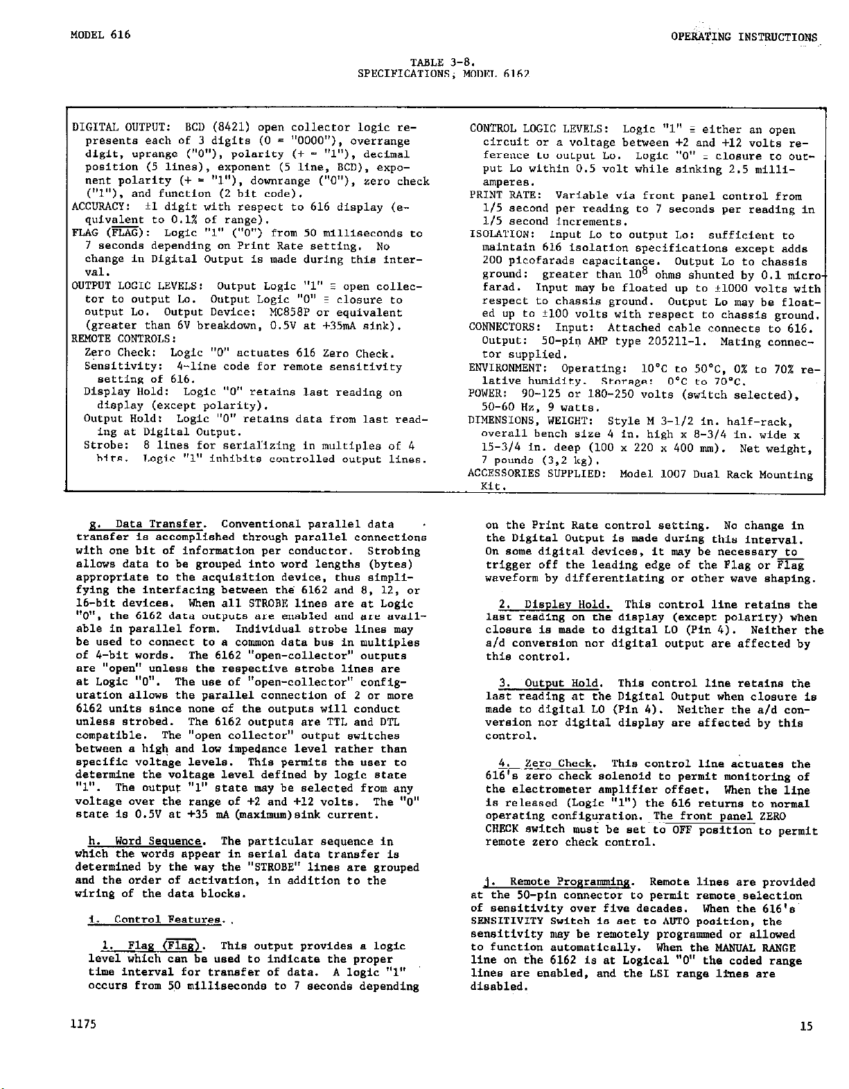
SPECIFICATIONS; MODEL 6162
TABLE 3-8.
IIGITAL OUTPUT: BCD (8421) open collector logic re-
presente each Of 3 digits (0 = "OOOO"), overrange
digit, uprange ("O"), palarity (+ = "l"), decimal
position (5 lines), exponent (5 line, BCD), exponent polarity (+ = "I"), downrange ("O"), zero check
("I"), and function (2 bit code).
rCCURACY :
quiva1ent to 0.1% of range).
QAG (FLAG): Logic "1" ("0") from 50 milliseconds to
fl digit with respect to 616 display (e-
-
7 eeconde depending a" Print Rate setting. No
change in Digital Output is made during this interval.
l"TP"T LOGIC LEVELS:
0"tp"f Logic "1" : open collecear to autput La. output Logic "0" : closure to
output LO.
Output Device: MC858P or equivalent
(greeter than 6V breakdown, 0.5V et +35mA sink).
!S-fOTE CONTROLS:
Zero Check: Logic "0" act"ates 616 Zero Check.
Sensitivity: 4-line code far remete eeneitiviey
setting of 616.
Display Hold: Logic "0" retains last reading on
display (except polarity).
Output Hold:
Logic "0" retains data from last read-
ing at Digital output.
Strobe: 8 lines for seriaIizing in multiples af 4
bite.
Logic "1" inhibits controlled output lines.
CONTROL LOGIC LEVELS: Logic "1" = either a" open
circuit or a voltage between +2 and +12 volta re-
ference to autput LO. Logic "0" E closure to ouep"f Lo within 0.5 volt while sinking 2.5 milliamperes.
PRINT RATE: Variable via front panel control from
l/5 second per reading to 7 seconds per reading in
l/5 second increments.
ISOLATION:
Input LO to output Lo: sufficient to
maintain 616 isolation specifications except adds
200 picofarads capacitance. Output Lo to chassis
ground:
farad.
greater than lo* ohms shunted by 0.1 micrc
Input may be floated up to flOO0 volts with
respect t0 chassis grand. Output Lo may be flaated up t" tlO0 volts with respect LO chassis ground.
CONNECTORS:
Input: Attached cable cennecte a, 616.
Output: 50-piq AMP type 205211-l. Mating co""ectar supplied.
ENVIRONMENT: Operating:
10°C t0 5ov, 0% to 70% re-
lative humidity. Storage: O'C to 70"~.
POWER:
90-125 or 180-250 volts (switch selected),
50-60 Hz, 9 watts.
DIMENSIONS, "EIGHT: Style M 3-l/2 in. half-rack,
overall bench size 4 in. high x B-314 in. wide x
15-314 in.
deep (100 x 220 x 400 mm). Net weight,
7 pounds (3,2 kg).
ACCESSORIES SUPPLIED: Model 1007 Dual Rack Ma,neing
Kit.
8. Da.8 Transfer.
Conventional parallel data
transfer is accomplished through parallel connections
with one bit of information per conductor.
Serobing
allows data to be grouped into word lengths (bytes)
appropriate te the acquisition device. thus simpli-
fying the interfacing between the 6162 and 8, 12, or
._..
lb-tat devlcee. when a11 STROBE lines are at Logic
"0". the 6162 data outputs are enabled end ere sveil-
able in parallel farm. Individual strobe lines may
be used to c~nlect te e cemmen data bus in multiples
of l-bit words.
The 6162 "open-collector" ~utpute
are "open" unless the respective strobe lines ere
at Logic "0". The uee of "open-callactor" configuration allawe the parallel connection of 2 or m"re
6162 unite since none of the outputs will conduct
unless strobed. The 6162 wtpute ere TTL and DTL
compatible.
The "open callectar" output switches
between a high and low impedance level rather the"
specific voltage levels.
determine the voltage level defined by logic state
,tl,,
The output "1" etete may be selected fram any
.
This permits the ueer to
voltage over the range of +2 and +12 volts. The "0"
state is 0.5V et +35 m.4 (maximum)sink current.
h. Word Sequence. The pa,rticular sequence in
which the worda appear in serial data transfer is
determined by the way the "STROBE" lines are grouped
and the order of ectiveti"", in addition to the
wiring of the data blocks.
i. Control Features.
1. Flag (m. This eutp~t provides a lagic
level which ce" be used to indicate the proper
time interval for transfer of data. A logic "1"
~ccure from 50 milliseconds ta 7 seconds depending
on the Print Rate contra1 setting. Na change in
the Digital Output is made during this interval.
On some digital devices, it may be necessary to
trigger off the leading edge of the Flag or Flag
-
waveform by differentiating or other wave shaping.
2. Display Hold.
This control line retains the
last reading on the display (except polarity) when
closure is made te digital LO (Pi" 4). Neither the
a/d conversion "ar digits1 wtput ere affected by
fhie control.
3. Output Hold. This control line retains the
last reading et the Digital Output when closure is
made to digital LO (Pin 4). Neither the a/d converaia" nor digital display ere affected by this
control.
4. Zero Check. This contra1 line e&uetee the
616's zero check solenoid to permit monitoring of
the electrometer amplifier offset. When the line
ia released (Logic "1") the 616 returns te "o-1
operating canfigl+ti0n. ~The front panel ZERO
CHECK awitch muet be set te OFF position te penoit
remote zero check control.
j. Remote Programming. Remote lines ere provided
at the 50-vi" connector to Kermit rem"te selection
of se"sit&ty over five decedes. When the 616's
SENSITIVITY Switch is eet to
AUTO
position, the
seneitivity may be remotely programmed or allared
to function automaticslly. When the MANUAL RANGE
line on the 6162 is et Logical "0" the coded range
lines are enabled, and the LSI range linea ere
disabled.
1175
15
Page 20
OPERATING INSTRUCTIONS
MODEL 616
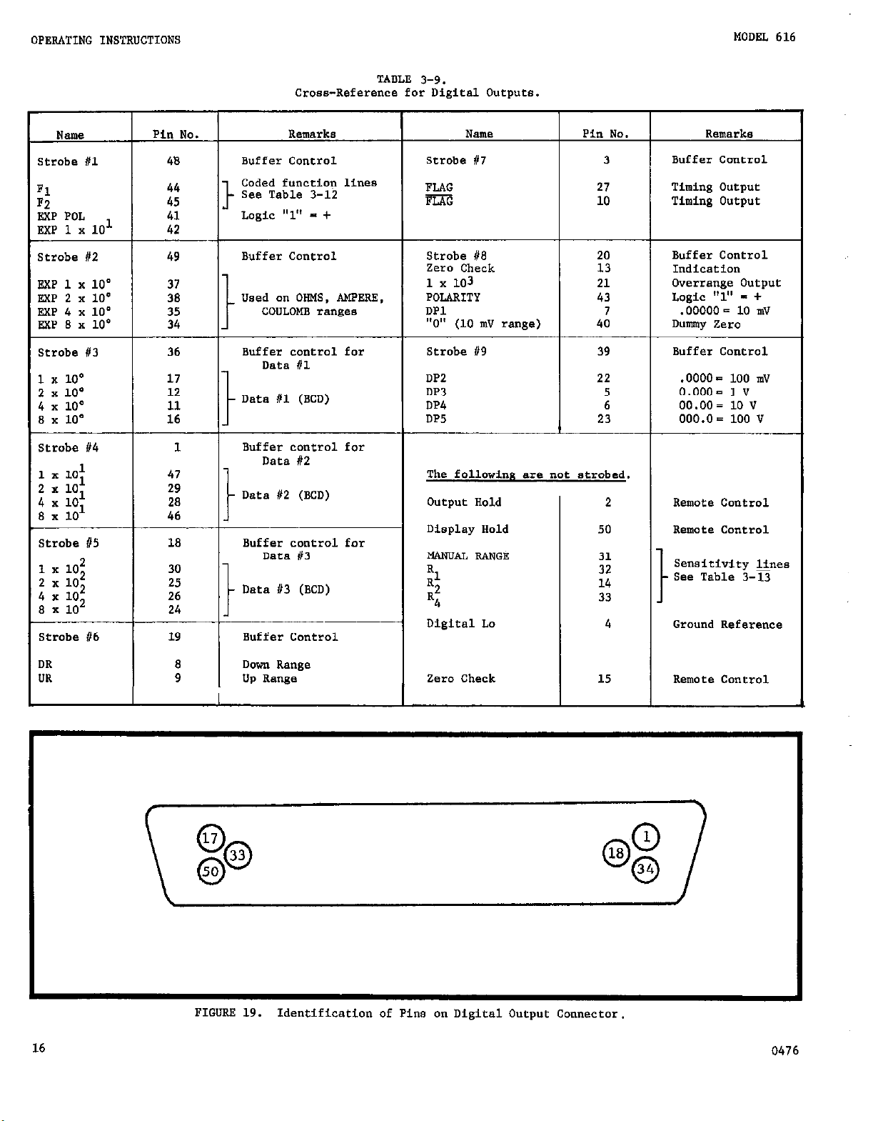
N8”e
Strobe Ul
Fl
F2
EXP POL
EXP 1 x lo1
1 x 10' 17
2 x 100 12
4 x 100 11
8 x 10' 16
1 x 10² 30
2 x 10² 25
4 x 10² 26
8 x lo2 24
Strobe #6
Pin No.
I
48
I
19 Buffer Control
I
DR
UR 9
I
a
Cross-Reference for Digital 0utp"ts.
Remarks
Buffer Control
Coded function lines
See Table 3-12
t
Logic "1" - +
Buffer Control
Used on OHMS, AMPERE,
COULOMB ranges
Buffer control for
Data 111
I
Data 111 (BCD)
t
Buffer control for
Data 112
Data 112 @CD)
t
Buffer control for
Data u3
Data #3 @CD)
t
Dmm Range
UP Range
TABLE 3-9.
Strobe #7
FLAG
FLAG
Strobe 88
Zero Check
1 x 10³
POLARITY
DPl
"0" (10 mv range)
Strobe 1/9 39
DP2
DP3 5
DP4 6
DP5 23
The following are not strobed.
Output Hold
Display Hold
MANUAL RANGE
3 32
R2 14
84 33
Digital Lo
Zero Check
Name
Pi" No.
3
27
10
20
13
21
43
4:
22
2
50
I
31
4
15 Remote Control
Buffer Co"rrol
Timing OUtput
Timing Output
Buffer Control
Indication
overrange output
Logic "1" - +
Dummy Zero
Buffer Control
Remote Control
Remote Control
sensitivity lines
-See Table 3-13
Ground Reference
Remarks
.ooooo- 10 m"
.oooo= 100 "V
o.ooo- 1 "
oo.oo= 10 "
ooo.o- 100 "
16
FIGURE 19.
Identification of Pins O" Digital Output Connector.
0476
Page 21
MODEL 616
OPERATING INSTRUCTIONS
--.
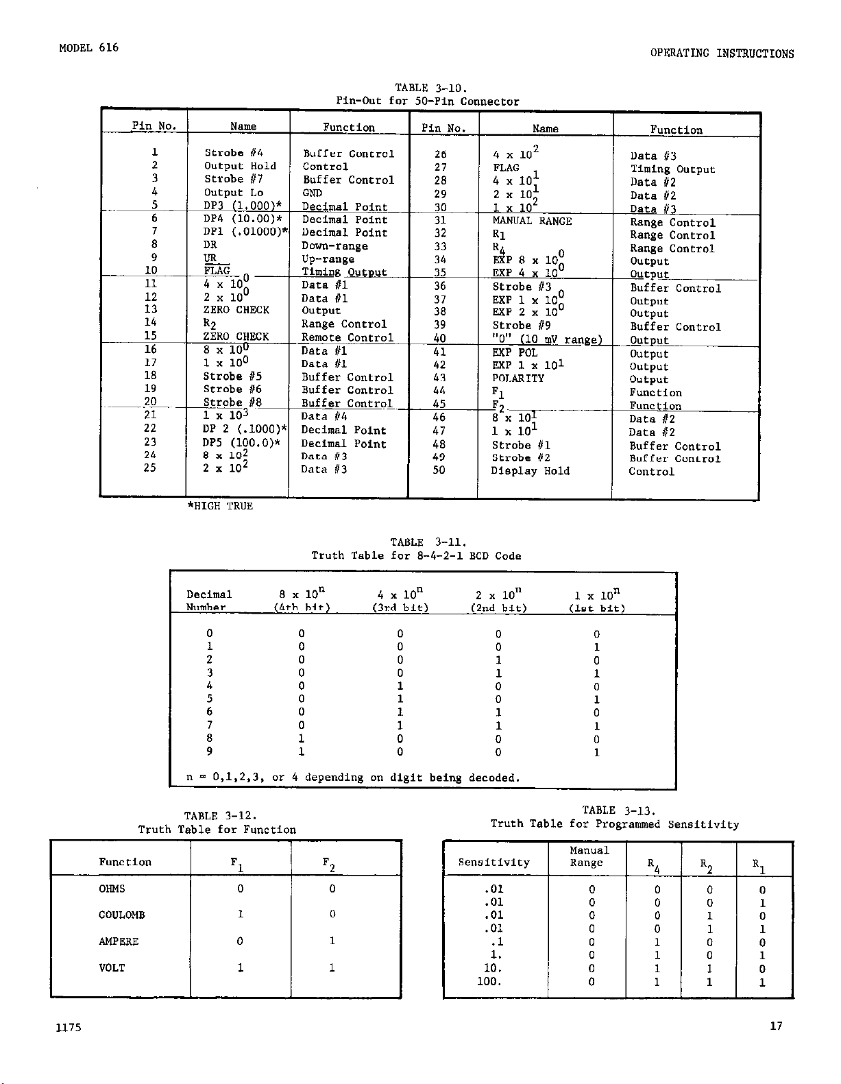
Pi" N,
0. Name
I
1
2
3
4
5
6
7
8
9
10
1%
11
12
13
14
15
16
17
18
19
20
21
-1x10³~-~
22
23
24
25
I
Strobe
output
Strobe
output
DP3
114
Hold Control
/17 Buffer Control
LO GND
(l.ooo)*
DP4 (lo.oo)*
DPl (.OlOOO)*
Buffer Control
Decimal Point
Decimal Point
Decimal Point
DR
1 up-range
FLAG
4 x 100
2
x 100
ZERO CHECK
R2
ZERO CHECK
8
x 10"
1 x 100
Strobe 1/5
Strobe ,,6
Strobe It8
DP 2 (.looo)*
DP5
(lOO.O)* Decimal Point
8 x lo2
2 x 10²
Timing Outwt
tuta Ill
Dsra 111
output
Range Control
Remote Control
Data #I
Data 01
Buffer Control
Buffer Control
Buffer Conrr&
Data i/4
Decimal Point
Data 113
tuta II3 50
pin-out for 50-P*" Co""eCtor
TABLE 3-10.
Functio"
Pin No. Name
I
26
1 27 / FLAG ,
28
I
29
30
31
32
1 34
35
36
37
38
I dP 8 x 10:
39 Strobe #9
40
41
::
44
45
46
47
48
49
Function
I
4
x
loL
4 x 101
2 x 101
1 x 10²
MAN"AL RANGE
Rl
Data 113
/
I Timing 0"fpue
Data j2
Data 1/z
Data #3
Range Control
Range Control
I oum,ut I
EKP 4 x 10"
Strobe 03
EKP 1 x
100
Exe 2 x 100
output
Buffer Control
Output
output
Buffer Control
"0" (IO "" range)
RKP POL
101
EKP 1 x
POLARITY
Fl
F2~
8
101
x
101
1 x
Strobe It1
Strobe ,,2
output
output
output
Output
FUnCtiO”
Func eion
IkIt* 112
Data /12
Buffer Control
Buffer Control
Display Hold Control
I
I
t--
,
Decimal
Number
n = 0,1,2,3, or 4 depending on digit being decoded.
TABLE 3-12.
Truth Table for Function
Function
Function
OHMS
OHMS
COULOMB
COULOMB
AMPERE
AMPERE
VOLT
VOLT
rT---!
0
1
F1
F1
0 0
0 0
1 0
1 0
0 1
0
1 1
1 1
TABLE 3-11.
Truth Table for 8-4-2-l SCD Code
2
8 x 10"
4
x 10"
x 10" 1 x 10"
(4th bit) (3rd bit) (2nd bit) (1st bit)
0
0
0
0
0
0
0
1
TABLE 3-13.
Truth Table for Programmed Sensitivity
MWl”81
0
0 0 0 1
0 0 1 0
0 0 1
0
0
0
0
F2
F2
Sensitivffy R*“ge
.Ol
.Ol
.Ol
.Ol
1
.l
1.
10.
100.
R4
0
1
1
1
R2
0
0 0
0
1
1 1 1
Rl
0
1
1
0
1175
17
Page 22
OPERATING INSTRUCTIONS MODEL 616
Truth Table for Serial Transfer
TABLE 3-14.
I,8
STR BE 6
8 9
I
I
1
,I
STROBE 7
19
3
27 10 I
L
,I
0
4 t Y c
A 6 C II
FIGURE 20. Suggested Hook-up far Data Lines.
1175
Page 23
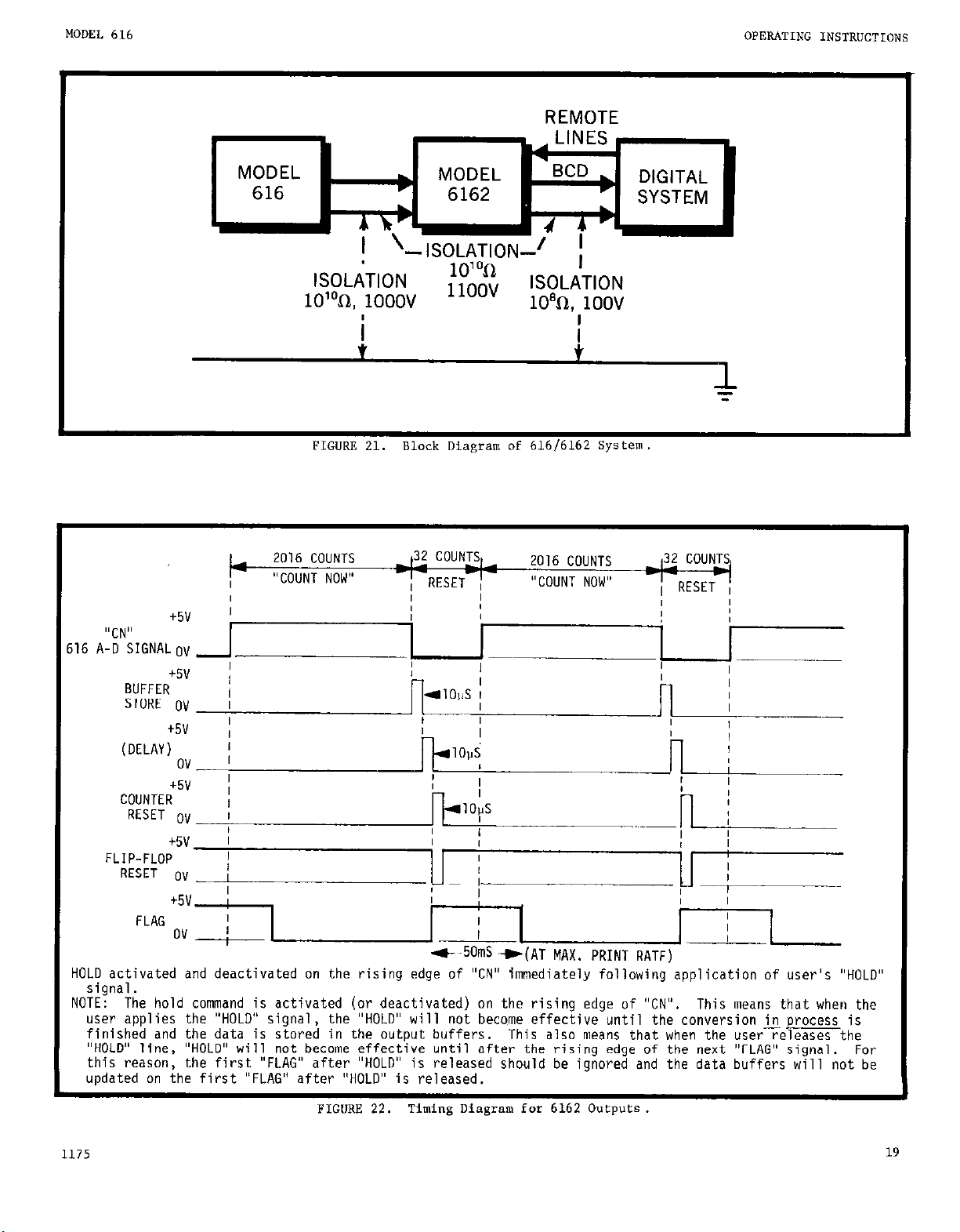
REMOTE
t5V
"CN"
16 A-O SIGNALOV
+5v
BUFFER
STORE OV I
+5v ;
(DELAY) Ov ;
COUNTER
FLIP-FLOP
RESET OV
+Yl
RESET OV I
t5v
t5V
FLAG
ov
A
MODEL
616
I
I
I
I
I
I
I
I
I
I
I
I
, MODEL
BCD
6162
A \+-
\1 A’-
1 ‘-IS~o$~;ON-’ 1
ISOLATION
lo’“cL, 1ooov
FIGURE 21. flack diagram of 61616162 System.
2016 COUNTS
"COUNT NOW"
1lOOV
I
ISOLATION
lo%, 1oov
2016 COUNTS
"COUNT NOW"
, DIGITAL
SYSTEM
:
HOLD activated and deactivated on the rising edge of "CN" tmmediately following application of user's "HOLD"
signal.
NOTE: The hold command is activated (or deactivated) on the rising edge of "CN". This means that when the
user applies the "HOLD" signal, the "HOLD" will not became effective until the conversion in process is
finished and the data is stored in the output buffers.
"HOLD" line, "HOLD" will not become effective until after the rising edge of the next "FLAG" signal. For
this reason, the first "FLAG" after "HOLD" is released should be ignored and the data buffers will not be
updated on the first "FLAG" after "HOLD" is released.
FIGURE 22.
Timine Diaeram for 6162 Oumuts.
This also means that when the user%leases the
Page 24

Page 25

MODEL 616 THEORY OF OPERATION
SECTION 4.
4-1. GENERAL.
describe the “O&l 616 circuit operation. The cir-
cuicry is located o” five printed circuit boards.
The circuits are arranged in functional modules to
facilitate troubleshooting and servicing. The 616’s
shielded input section houses the electrometer amplifier and range switch.
4-2. ANALOG CIRCUlTKY
a.
Input Amplifier. This amplifier A1 is show” in
simplified form in Figure 24. (Refer t” schematic
25764E). The input signal applied between HI and LO
(5120) is amplified by the input MOS-FET amplifier
composed of transistors Q101A and Q101B.
q102A and Q102B are used for aver-voltage protection
(base-emitter connected). Integrated circuit QA101
provides high gain (approx. 100,000) for the electro-
meter amplifier section. Potentiometer R123 is a*
internal zero adjustment used for calibration purPOSW. Potentiometer K119 is a front pane1 ZERO
control with adj”stme”t capabilitv of a~oroximatelv
3 In”. Transistors Q105 and QlOk are comp1ementa;y
output stages which provide a maximum of 1200 volts
at the “Xl” terminal (Jll8). The electrometer amp-
lifier ia connected in a unity-gain configuration.
sistance between HI and LO is greater than
ohms in “VOLTS” functia”.
This section contains information to
Tranafseors
THEORY OF OPERATION
Shunt (NORMAL) Mode Operation.
b.
schematic 257643).
trometer amplifier is connected as a unity-gain
buffer amplifier with a” input resistance greater
than 2 x 10¹⁴ ohms.
ed in decade steps from IO11 ohms LO 10 ob,,,s by
selecting the desired shudt resistor a” the AMPERE
positions of the RANGE switch. Resistors RIO1
through Rlll are switched into the citzuit shunting
the HI and LO terminals. The shunt resistor can-
“ected in the circuit is numerically the reci rocal.
of the AMPERE position selected (that is
10% resistor).
C. Feedback (FAST) Mode Operation.
schematic 25764E). In the “FAST” mode, the electro-
meter amplifier is connected in a feedback amplifier
configuration. I” AMPERE, CO”LOMB, or OHMS functions,
the range element (resistor “r capacitor) is connect-
ed be~wee” HI and GUARD. Input resistance on AMPERE
function is determined by the feedback resistor and
the open-loop gain, where:
Ri = RF (K = 50,000 minimum)
FOT example, on 10-11~ range, R* = 2 x 10611. I*p”t
voltage drop for full range in,.~ut current would be
less than 20 microvoles.
In the “NORMA,.” mode, the elec-
Input resistance may be decreas-
K
(Refer to
-1% :
10
(Refer to
1175
IN
RANGE
INPUT
AMP
I
POLAR/TY
A-D
- DETECTOR - CONVERTOR
i
i
11
LSI
CHIP
-DRIVERS - DISPLAY
21
Page 26

THEORY OF OPERATION
Zero Check Operation. (Refer to schematic
d.
257643).
operates e relay solenoid (KlOl) when set to ZERO
CHECK. In the energized etate (as ahown on the
schematic) the relay contact is closed. The closed
contact makes e co~ection between the FET amplifier
illP"f and GUARD (5119) es fallows:
The front panel ZERO CHECK switch (5102)
MODEL 616
TABLE 4-1.
Voltazxe Gain
1. Normal Mode.
made between resistor R124 and input LO. Notice
that the input HI terminal is shunted to LO by a
10%
resistor
2.
Fast Mode.
made between resistor R124 and GUARD. Notice
that the input HI terminal remains connected to
the electrometer amplifier input. Ill AMPERE, OHMS,
or COULOMB functiona, the feedback element is
shorted out so that no voltage can be generated
across the amplifier feedback.
remote zero check capability is provided
when the Model 6162 is connected to the
The connection at Pll3D is in para-
616.
llel with the front panel switch. The
front panel ZERO CHECK switch should be off
when using the remote zero check feature.
e. Voltage Sensitivity. This amplifier A2 is shown
in Figure 24.
ond stage variable-gain amplifier is composed of e
FET stage (Q301A. 4301B) and an ineegrafed circuit
QA301.
F) where:
Gain is determined by resietors RN301 (A to
(Refer to schematic 25776D). The eec-
In this mode, a connection is
(~112).
In this mode, a connection is
Gain = 3 (See Table 4-l.)
RI
10.00 ” 500m
100.0 " 500KO
1. Gain setting. Resistors
are connected in parallel combinations to achieve
the proper gain.
ting, the gain is determined by the series combination of resistors RN3OlB and R303. Potentiometer
R303
10 m" sensitivity setting. For each succeeding
sensitivity, the resistors are switched into the
circuit as shown in Table 4-2. Potentiometer
R304
sensitivity setting.
S‘XSiti”itY
I
.01000v 50 Mn (RN301+? + R303)
.lOOO ” 5 MCI (RN301B + R303//RN301C)
1.000 ”
10.00 V
100.0 "
La a calibration adjustment for the
iB a calibration adjustment for the 1OOV
On the 10 mV sensitivity set-
TABLE 4-2.
Gain Switching
Feedback Resistors Used For Gain Set.
500 K$? (RN301B + R303//RN3OlC//RN3OlD)
50 Kn (RN301B + R303//RN301C//RN301E)
5
KC (All above//RN301F + R304)
50
Kn 0.1
5
Kfl 0.01
RN3OU
to RN301F
I
22
INPUT
0
LOW 0
UNITY GAIN
BUFFER SENSITIVITY
SETTING
FIGURE 24.
Simplified Diagram of Amplifier Section.
1 VOLT
0
1175
Page 27

MODEL 616 THEORY OF OPERATION
Gain Selection Logic. (Refer to schematica
2.
25776D, 257788).
used to determine voltage sensitivity.
A three line ranging code is
The coding
for the three lines (R4, R2, Rl) is given in Table
4-3.
TABLE 4-3.
Ranging Logic
where 0 = open state
1 = t5v *ate
3. Zero
Adjustment.
Potentiometer R311 is an
internal zero adjustment for calibrating the "lv"
recorder output.
f. Ammeter Operation. (Refer to schematic 25764E).
In the AMPERE mode, a range resistor (RlOl through
Rlll) is connected between input HI and GUARD. The
current-Lo-voltage conversion 1s determined by the
following relationship:
ER = voltage developed across R
I - input current
R = range resistor
In the "NORMAL" mode, the input voltage drop is
equivalent to
drop is a funct on of open loop gain (typically
ZO!JV).
The use of the FAST mode is limited to
In the "FAST" made, the input
"H.
ranges 10m5A to lo-llA due to loading and stability
considerations.
1175
23
Page 28

THEORY OF OPERATION
FIGURE 27. Coulombmeter Configuration - FAST Mode.
g Coulombmeter Operation.
257k4E).
(Cl01 through Clll) is connected between input HI
and GUARD.
determined by the fallowing relationship:
h. Ohmmeter Operation.
257643).
connected into the electrometer circuitry. The
voltage sensitivity is selected as in VOLTS operation.
source and a series (RANGE) resistor. The series
resistor is selected in decade steps in the OHMS
position (resistors R105 through Rlll). The voltage source is provided by dividing down from a +12
volt reference supply.
internal calibration adjustment.
In the COULOMB mode, a range capacitor
The charge-to-voltage conversion is
EC = $ Ii dt -z
EC E voltage developed acrow C
C - range capacitor
Q ,- stored charge
In the "OHMS" mode, a current Llource is
The current source is composed of a voltage
Potentiometer R114 is an
(Refer to schematic
(Refer to schematic
Ohmmeter Divider Network
Ohms
Range
The current developed by the ohmmeter circuit is
determined as follows:
where I = Furrent in amperes
R
Total
12K 1.0101cn
12K l.OOOK61
12K 1. OOOKQ
12K
12K
12K l.OOOKQ
12K l.OOOKn
12K
1-E
E - voltage as in Table 4-4.
R = range resistor (R105 through Rlll).
TABLE 4-4.
R,
1.ooom
1.oooKo
100
E = 12 Rl/(Rl+R2)
-.A&-
10.990Kn
ll.OOOK
ll.OOOK
ll.OOOK
ll.OOOK
ll.OOOK
ll.OOOK
11.9 K
E
1.01 v
1.00 v
1.00 v
1.00 v
1.00 "
1.00 v
1.00 "
0.1 "
24
FIGURE 28. Ohmmeter Configuration - NORMAL Mode.
1175
Page 29

MODEL 616
i. Polarity Detection Circuit.
schematic 257760). This circuit detects the
polarity of the input signal and triggers the
polarity display circuitry,
1. First Stage Amplifier. When the input to
intearated circuit
D301-conducts causing the a&ifier ti op&?ate
with a gain of 2X (inverting). A negative-going
input to QA302 is not amplified due to the block-
ing action of diode D301 which prevents the output of QA302 from going positive. Transistor
Q306 conducts to maintain feedback around QA302
and therefore provides polarity information co
turn-off the "minus" polarity.
2.
Second Stage Amplifier. Integrated circuit
QA303 is used as an inverting summing amplifier.
Far a positive-going input to the polarity detec-
tion circuit, QA303 provides a gain of -1 for a
net output of +lV maximum. When the input is
negative-going, the inputs to
provide a net oucpuc of +lV maximum.
3. Adjustments.
ternal calibration control for adjustment of
amplifier zero. Potentiometer R307 is an internal
calibration control for adjustment of gain in the
summing amplifier QA303.
OA302
is msitive-noina. diode
Potentiometer R305 is an in-
(Refer to
QA303
are summed to
4-3.
ANALOG-TO-DIGITAL CONVERTER.
schematics 25776D. 25778B). The a-to-d converter
operates on a charge balancing principle. The circuit operates only with unipolar inputs. A block
diagram of the converter is shown in Figure29. The
positive output of the polarity detector circuit
drives the integrator amplifier QA304 negative. The
integration rate is determined by the input level,
resistors RN304A and RN304B and capacitor C308.
As the integrator goes negative, the threshold
detector (amplifier QA305) output goes to a positive
level.
the "J" input of the J-K flip-flop (the "K*' input
is a logic "0").
for the integrator are determined by the state of
the Q output on the J-K flip-flop. When the Q
output Se high, diode QA306 D is back biased off
and the integrator can only be charged by the
polarity detector output. When the Q output is
low, diode QA306-D is forward biased and discharge
of the integrator is possible.
states can be changed only when a clack pulse is
present, the charge/discharge periods are a function
of the clock frequency.
is free-running and has a timing period of 2016
Counts. The digital reading is derived by counting
clack pulses in the discharge pkriod. Far example,
a 1 volt input would result in a total count of 1000
clock pulses.
counts.
counts, the remaining 32 counts are needed to stop
the BCD counter, strobe the ED counter information
into latches, reset the BCD counter to zero, and
initiate uprange or downrange (or overrange). The
conversion rate is approx. 0.2 sets/conversion
(2048
A positive level represents a logic "1" *t
The charge and discharge periods
The a-to-d conversion cycle
One complete conversion cycle is 2048
In addition to the timine wriad of 2016
counts at a 10 kHz clock rate).
(Refer to
Since the Q and Q
I j
*REF
- 9V REF;
A-D CONVERTOR
INTEGRATOR
,t CL$,L~;T’--------
I K
9K
IEi
I
I
’ LSI W/P
THRESHOLD
DETECT
,
J
CLOCK
0
- --
Page 30

THEORY OF OPER**ION
MODEL 616
AUTO-RANGING CIRCUIT.
4-4.
257788).
(QA408) with exception of decoding diodes D3Ol.A
through D301H and FET switches Q302 through Q305.
The threshold input (TH) and current switch (CS)
signals are used to determine the proper range.
Ranging is bidirectional so that upranging or
downranging to an adjacent range occurs. The a"toranging feature is defeated by grounding pin 6 (MS)
on LSI QA40S.
4-5.
four LED, 7-segment readouts plus a polarity/aver-
range readout.
plexed 80 that only eight lines are driven at a time.
a. Multiplexing Circuit. This circuit is contained
in the LSI QA20S.
four multiplexing lines which turn on the anodes of
each seven segment readout. Four of the lines are
used for each of the four digits. Polarity, decimal
point, and dummy zero (an the .OlOOOV ranple) are not
multiplexed.
to provide sufficient drive for transistors Q405
through Q407 respectively. Each anode of each LED.
readout is pulled up to approx. +lO volts to light
a particular digit.
b. Display Coding. Each dieplay module has separate
cathode connections for each segment as given in Table
4-5.
This circuit is located on the LSI module
DISPLAY DRIVE. The 616 display is composed of
The display drive circuit is multi-
The dieplay is controlled by the
QA401A through QA4OlD are used
(Refer to schematic
I
Numeral
8
9
decimal
FIGURE 31.
Display Codi
A,B,C,D,E,F
B.C.
A,B,D,E,G
A,B,CL',G
B.C,F,G
A,C,D,F,G
A,C,D,E,F,G
A,B,C
A,B,C,O,E,F,G
A,B,C,E,F,G
decimal
Digital Display.
TABLE
4-5.
Fills
1,13,10,8,7,2
13,lO
1,13.8,7,11
1,13,10,8,11
13.10.2.11
i,io,S,;,ii
1,10,8,7,2,11
1,13,10
1,13,10,8,7,2,11
1,13,10,7,2,11
6
CS
TH
-OUTPUTS
RANGE
MULTIPLEXER
TO READOUTS
FIGURE 30.
26 1175
Functional Block Diagram of Large Scale Integrated Circuit.
Page 31

MODEL 616
THEORY OF OPERATION
c.Dacima1 Point (Sensitivity) Codingl Three
coded lines are used to generate the decimal point
drive.
The lines are designated Ri, ;?;, ;;it4;or
Inverters QA404A.C.E ,,rovide B lot c
a corresponding logic-"0" stare (&xure to LO) on
any of the lines. !&en used in the AUTO mode, a
fourth line is used to defeat the automatic ranging circuit.
The remote enable line (MR) is activated "hen a connection to LO is made at pin 6 (MB)
on LSI OA408. A truth enhle for decimel point logic
is given in Table 4-6.
TABLE 4-6.
Decimal Paint Coding
S*nSitiVity
S*tthg
B4
%
5
.01000 0 x x
.lOOO
1 0
0
1.000 1 0 1
10.00 1 1 0
100.0
1 1 1
d. Overrange Indication. Overrange is indicated
by diode network DN403. Transistor Q403 controls
the cathodes for segments A,D,F,E co display a "0".
When transistor Q403 is turned off, the display indicates a "1" since segments S and C are always
eurned on (pins 10 and 13 are connected to LO).
e. Dupuny "0" Indication.
When the 10 millivolt
range is selected, the 616 display indicates a
fifth digit (DN402) and decimal paint. Transistor
Q402 controls the cathodes for segments A,B,C,D,F,E
to display a "0". Transistor Q402 is turned off
when R4 is high (QA404A = low).
f. Polarity Indication.
The polarity display DN401
is controlled by eranaistor Q401. The minus sign is
always lighted.
Additional segments are turned on
for rhe plus sign.
8. Overload Indication.
The LSI module (QA40S)
contains additional circuirrv for overload blankine
of the display.
When the display exceeds 200 volt:,
the circuit causes a blinking action of the three
least significant digits. The display reads properly
up to 201.7 volts (001.7 max.).
b. Decimal Point. This circuit is composed of
inverter stages QA405A.B.C which provide sufficient
drive for optical isolators in the Model 6162. De-
cimal point is coded in three lines B4. R2, Rl as
shown in Table 4-6.
4-s.
POWER SUPPLIES (Schematic 25777D).
a. Primary Power. The Model 616 can be operated
over two ranges of line voltage. Switch 5201 haa
two line voltage positions a.8 follows:
117V: 9OV - 125V rms range
234V: 18OV - 250V rms
50-60 Hz, 9W
Fuse (F201) must be selected for each line voltage
range as follo"s:
117": 3116 ampere, 3AG SLO-BLO
234V: l/l0 ampere. 3AG SLO-BLO
b. Secondarv Power.
The Model 616 power supply
is composed of four separate supplies. Transformer
T201 provides four center-rapped secondary windings.
1. i275V Unregulated. This supply taps a-c
power from secondary windings l-2-3 of T201. Diodes
0201 through 0204 form voltage-doubling supplies.
Outp"t voltage is approximately 275 volts at 2
milliamperes (at nominal line voltage). Ripple is
a,qn-oximately 2 volts peak-to-peak at no load.
2. t12" Regulated.
This supply taps n-c power
from secondary windings 6-7-S of T201. 0205 is
a four-diode full-wave bridge. Integrated circuit
QA201 provides a regulated f12 volts at 10 milliamperes. Ripple is approximately 1 millivolt
peak-to-peak at nominal loading.
3. -9" Regulated. This supply also utilizes
D205 for full-wave rectification. Zener diode
0206 provides a regulated voltage of -9" at 5
"illi*"peres. Ripple is approximately 3 milli-
volts peak-to-peak.
REFERENCE OSCILLATOR. The reference frequency.
4-6.
(clack) circuit is composed of integrated circuit
QA406 and other fixed components forming a freerunning 0scillaP.x.
The oscillator operates af
frequency of approx. 10 kHz. The output of rransistar Q411 is a clock pulse between -0.7 volt and +5
volts dc with a 5 microsecond pulse widrh.
MISCELLANEOUS CIRCUITS USED FOB 6162, These
4-7.
circuits are used to generate signals or signal
levels for the Model 6162 Isolaced Output/Control.
a. Gated Clock.
This circuit is composed of in-
verters OA405D.E.F and NAND eates OA407A.B.C. The
drcuic Abi&~'~i~~8l~ fr& the is1 && 4
clock to provide a gated clock "GC". This signal and
"CN" are used to generate BCD outputs in the Model
6162.
1175
4. +5V Regulated. This supply caps a-c power
from secondary windings 9-10-U of TZO1. Diodes
0207 and 0208 form a full-wave rectifier. I"t*grated circuit QA203 provides a regulated output
of +5 volts at 200 milliamperes. Ripple is spproximarely 1 millivolt peak-to-peak.
5. +lOV "nregulaced.
This supply utilizes the
unregulated outpuf of the full-wave rectifier 0207-
DZOS. Ripple is approximately 1 volt peak-to-peak
at 200 milliampere loading.
6. -12V Regulated.
This supply taps a-c power
from secondary windings 13-14-15 of T201. Diodes
D209 and D210 form a full-wave rectifier. Ince-
grated circuit QA202 is a regulator element.
Transistor Q201 is a series-pass regulator. Out-
put voltage is -12V at 50 milliamperes. Ripple
is approximately 2 millivolts peak-to-peak.
27
Page 32

THEORY OF OPERATION
MODEL 616
TABLE 4-7.
k7.n ldentlticetl0" *or LSI
Pi" No. Designaeian Function
1
F
Segment drive +5" = ON, 0" - OFF
2 G Segment drive +5V - ON
3
Tl
Multiplex Line +5V = ON
4 T3 Multiplex Lice t5V = ON
5 HOLD
6 MR
7
8
TH
CLK
Display hold +5v = "OLD
Range Enable 0" = inhibit autoranging
Threshold input +5v or -12V
Clock Pulse
A~prox.~
9 B Segment drive +5V = ON
10 A Segment drive +5v = ON
11 D Segment drive
+5" - ON
12 E Segment drive t5V = ON
13
C
14 cs
15 DP
16
$44
17 TO Multiplex line +5v - ON
18
Fl
19 F4
20
21
22
23
24
25
26
27
28
Segment drive +5" = ON
Current Switch +5V = integrate mode
No connection
No connection
-____
Power
Power
CO"lSOtl
Count Now
Multiplex line
0"
+5v
+5v
-12v
OV
+5v - 2016 counts
+5v = ON
Range Line
Range Line
See Table 4-6.
Rmge Line
___
0"
Voltage
Levels
,10kHz_,~~+SV to -lV
_--
-__
4-9. DIGITAL OUTPUT (Refer to schematic no'e 25715D,
25716D, 25717C, and 25823C).
a. Isolatia" Circuitry. Isolation of electrometer
LO and diuital Outout Lo is achieved throunh the use
of a" opt&ally c&led isolator for each Big"81
transmitted between the 616 and 6162. The isolators
are NPN types and provide greater than 10lOn isola-
tion resistance.
diodes are connected to +5 valts.
The anodes of all light emitting
The diode conducts
whenever the cathode is connected law (a 3300 current
limit resistor is used with each input). The output
of each isolator transistor is connected in e grounded emitter or emitter-follower configuration.
b. Decade C~u"ters.
The Model 6162 utilizes three
decade cwnter stages QA201, QA202, and QA203 for
"l", "lo", and "100" respectively. Each integrated
circuit provides BCD information using four linea
identified as 1 x lo", 2 x lo", 4 x lo", and 8 x 10".
Storage Registers.
C.
Individual storage registers
are used to control data flow to the ~"tput buffer
stages.
Integrated circuits QA205, QAZOk, and QA207
are enabled by the output of QA223A (ENB).
d. Buffered Output Stage. Each buffer ia composed
qf a Keithley Part No. IC-22 NAND gate (four gates
per circuit module).
The buffers utilize "open collector" output transistors. Each circuit module is
connected to a" individual STROBE control for mon-
itoring two or more 6162 autputs connected to a single
outpur bus.
Each set of four buffers is enabled
whenever the Strobe line is pulled davn to digital
10W. Each STROBE circuit consists of a" inverter
stage (Keithley X-32), a 4.7 kilahm pull-up resistor,
and a protectian diode (Keithley RF-39).
e. Print Rate Control.
Print rate for the Model
6162 consists of a timing circuit composed of integrated circuit QAloS, resisrar X116, pOte"tiometer
R115 and capacitor ClOl. Patentiometer R115 permits
continuous control of Print Rate from l/5 second per
reading to 7 seconds per reading. The Print Rate
cantrol has no effect on the Model 616 display rate.
f. Flag Circuitry. The Flag autput is generated
by integrated circuit QAloS. The oucput of buffer
stage QA222C is high far a length of time established
by the Print Rate Control. No change in the digital
output is made during the interval when Flag is high.
(Flag is Iv,,).
g. BCD Hald Circuit.
This circuirry inhibits the
Enable oulae which in turn holds the infwmatio" in
the s&-age registers.
ever DlOl is closed t" wtput low.
The Hold is activated when-
Integrated circuit
QA109 is a flip-flop which is set by m.
h. Display Hold.
This circuitry controls the
display driver in the Model 616. The Display Hold
1s activated whenever D102 is clased to output law.
1175
Page 33

MODEL 616
SECTION 5. ACCESSORIES
5-1. GENERAL. me following ‘(eithley acces.sories
can be used with the Model 616 co provide additional
convenience and versatility.
Model 6101.4 Shielded Probe
Description:
The Model 6101A is a shielded cable with B needle-point
probe
and 30 inches of low noise cable terminated by a
UHF COn”eCtor.
Model 61018
Description:
The Model 61018 is a shielded cable wieh a “gripping
type” probe and 30 inches of low noise cable terminated
b,y a WF Co”“ectOr.
5-2. OPERATING INSTRUCTIONS. A separate Instruction
Manual is supplied with each accessory giving complete
operating information.
Shielded Probe
Model 6103C Divider Frobe
Description:
The Model 6103C is a shielded cable with a needle-point
probe
and 30 inches of low noise cable terminated by a
UHF connector. The
orobe
includes a 1OOO:l voltwe
divider with a 4.5 X’ 101ln resistance. Accuracy Is
25% at 30 kilovolts.
Model 6102A
Description:
The Modei~ 610% is a shielded cable with a needle-point
probe and 30 inches of low noise cabic terminated by a
UHF connectorlO The probe incl~odes a 1O:l voltage divider with 10 il input resistance. Accuracy is z&X at
1000 volts.
Divider Probe
0577
29
Page 34

ACCESSORIES
MODEL 616
Model 6011 Input Cable
Description: The 6011 is a low-noise triaxial cable,
30” long, terminated by three color-coded alligator
clips.
input.
no. ~3-141 connector and part no. SC-22 low-noise cable.
IleWZk-iptiCXl: The 6301 is a guarded triaxial cable,
3 ft. long, terminated by a probe for making point-topoint measurements.
This cable mates directly with the triaxial
The cable is fabricated using a Keithley part
Model 6301 Guarded Probe
Model 1531 Gripping Probe
Application: The 6011 may be used far measurements
which require a triaxie1 connection, especially when
the input I.0 is floated above
Application: The 6301 may be used for measurements
which require a triaxial cable with a guarded pfZbzhms,~
having an insulation resistance greater than 10
CASE
ground.
e
SC-22
cs-141
Description: The 1531 is a triaxial cable, 3 ft. long, Application:
terminated by a special gripping-type probe.
insulation resistance is greater than lOlo ohms.
probe is rated far off ground measurements up to 500 ”
Hi
Lo Lead
Description: The 6012 is an adapter for mating the
triaxiel input end UHF (coax) type connectors. This
adapter can be used with Models 6101A, 61018, 6103R,
6102A, etc.
The 1531
The
Model 6012 Triax-to-Coax Adapter
which require a triaxial cable. The probe permits
convenient connections to the circuit under test due
to the gripping feature.
CS-64
The 1531 may be used for meas”rements
es-141
30
1175
Page 35

MODEL 616
ACCESSORIES
Mod>1 6106 Elect,
Description:
The Model
blob
contains a group of the most useful
leads and adapters for low current measurements. All
components are housed in a rugged carrying case with
individual compartments.
Models 2501, 2503
:ometer Connection Kit
Parts List:
Description NO.
Cable, Xl”, UNF to clips
Cable, 24”, UHF to UHF
connector, UHF to UHF 3
Adaptor, UWF to BNC 4
Adaptor, UHF to BNC
Adaptor Tee, UHF to “HE
Adaptor, Binding Post 7
The two cables (Items 1 and 2) are coaxial shielded
leads useful for connections where low noise is essen-
tial. The 24” cable (Item 2) can be used to interconnect two instruments having UHF receptacles. The 30”
cable (Item 1) can be used to connect to the circuit
under test through the use of clip leads. A bind~ing
post adapter gives easy access to the electrometer
“high” terminal. Two UHF femal couplers (Item 3)
permit cables to be connected together. The “HP “tee”
connector simplifies galvanometric cUrrent measurements
when using a current source and electrometer or pica-
ammeter.
Adapters (Items 4 and 5) are useful for con-
version from UHF to BNC terminations.
Static
Defector Probes
Item
1
2
5
6
Keithley
Pam NO.
19072C
18265C
c-5
m-115
CS-172
lx-171
190718
Description:
The Models
2501 and 2503 are specially designed de-
tector~ used to measure static charge on plane surfaces.
Either Drobe must be used with an electrometer
Model 2501:
The 2501 is useful for measurements of charge on flat
surfaces.
The static head is 3 inches in diameter.
Recomended spacing is 318” from the surface for
lO,OOO:l divider ratio. The 2501 is calibrated such
that a 1 volt deflection on the electrometer con-e-
spends to 10 kilovolts of static charge.
Model 2503 :
The 2503 consists of a rigid probe l/2 inches in diameter.
probe.
Operation is similar to the use of the 2501
Model 6107 p” Elecrrode Adapter ,- Model 6107 p” Elecrrode Adapter ,Description: Description:
The Model 6107 is a test fixture which simplifies cm-
nections to the electrometer when making p” measurement.3.
factured
The
in the diagram.
The adapter can be used with electrodes man”-
by
Leeds &Northrup, Coleman
and Beckman.
6107 can be used far guarded measurements a~ shown
A
voltage-to-p” conversion chart is
supplied with the 6107.
------------1
I
A? Pip Jd
LJ2 ,
Page 36

ACCESSORIES
Model 6104 Test Shield
Description:
The Model 6104 is a shielded test box for two-terminal
or three-terminal connections. The ‘INPUT terminal is
teflon insulated.
Applications:
1. TWO Terminal Connections. Resistance measurements can be made conveniently using the INPUT and
GROUND terminals on the Test Sax. Connect the elec-
trometer to the SNC output. Use the electrometer in
NORMAL
mode
for ohms
measurement.
MODEL 616
2. Three Terminal Connections. The GUARD output
on the Mode:
616 electrometer can be used for re-
sistance measurements where the effects of cable capac-
itance may be significant.
INPUT and EXT terminals.
the GUARD output an the electrometer.
erometer
In FAST mode for ohms measurement.
Connect the unknown between
Connect the EXT terminal to
Use the elec-
Model 6105 Resistivity Chamber
Description:
The Model 6105 is a guarded test fixture for measure-
ment of surface and volume resistivities. The chamber
Fs designed in accordance with ASTM Standard Method of
Test for Electrical Resistance of Insulating Materials,
D257-66.
The 6105 can be used in conjunction with an
electrometer and voltage supply.
Applications:
Resistivity can be determined by measuring the current
through a sample with a known voltage impresaed. The
measurement can be made most conveniently when B set
of electrodes are used which can be calibrated in terms
Of surface or volume resistivity. The Keiehley Model
6105 Resistivity Adapter has been designed for use with
a Keithley electrometer and an optional high voltage
supply such as the Model 240A.
32
1175
Page 37

MODEL 616
MAINTENANCE
SECTION 6.
GENERAL. This section contains information nec-
6-1.
essary to maintain the instrument to published speci-
fiCSltiO"S.
REQUrKED TEST EQUIPMENT. Minimum requiremenes
6-2.
for test equipment are given in Tables 6-l and 6-6.
PERFORMANCE "ERIFICATION.
6-3.
procedure to verify proper operation of the instru-
ment .
Performance of the instrument is based on an
operating telnperature between 20°C and 3o"c and relative humidity less than 70%.
Preliminary set-"E.
a.
set the Line Switch to 117 or 7.34" depending
1.
on the line power available.
Fuse Check:
2.
Verify that the appropriate line
fuse is installed.
117": 3116 ampere, 3AC, SLO-SLO (Keithley F"-29)
234V: l/l0 ampere, 3AG, SLO-BLO (Keithley R-40)
3. connect the power cord to a variable transformer which has been set to 117" t 1" or 234V I
2" depending on the line power available.
"se rhe following
MAINTENANCE
5. Turn the instrument power on and allow the
instrument to stabilize at ambient temperature for
at least l/2 hour. Record the temperature so that
temperature coefficients can be utilized as necessary.
b. Voltage Accuracy Check.
1. Select NORMAL mode and VOLT function.
2. Select the AUTO SENSITIVITY mode.
3. Place ZERO CHECK switch on. The display
should indicate .OOOOO volts.
the front panel ZERO control to obtain a rero reading with the polaricy indicator blinking on and off.
4. Place ZERO CHECK switch off.
5. Apply dc voltages to the in,xe of rhe Model
616 as given in Table 6-2 using Voltage Source (A).
TABLE 6-2.
Voltage Accuracy Check
source Display
Accuracy
If necessary, adjust
Reading
Reading
Tolerance
Connect the shorting link (on the rear panel)
4.
between LO and GROUND.
FIX maximum operator safety,
make certain that the chassis is connected to earrh
ground by way of rhe third conductor on the line
cord or by way of a separate clip lead from GROUNU
to earth ground.
TABLE 6-1.
Item Description Specification
A Voltage Source (DC), lOm" iO.O3% accuracy
to 100" in decade steps
(For 1OmV range use 1O:l divider)
B
Resistance source, 1050 to ?0.05%, 105n f0 1070
1O120 in decade steps
f0.2%, 1oSn
?0.5%, 1oQ to 101*0
c
Current Source, lo-lA to
iO.O5%, lo-IA to lo-4A
10-4A
D
current source, lo-?+ ~to
tO:b;$ l&5A to 10-7A
lo-'A Ranges
E
current source, 10-g to
lo-=A
LtZ%, 10-8A
0.6%, 10-gA to 10-llA
10 m"
100 Ill"
0.03%
0.03%
1" 0.03%
10 " 0.03%
100 V 0.03%
Fluke, Mode1 341A
) ,I)
GK 1455BH (divider for 10,~")
GK 1433, Keithley Model 5155
Fluke, Model 3330B
4
Fluke, Model 341A, and GR1433
see Note 1.
Keithley Model 261.
3 11, C.d :,; : i
.01000 " t3 digits
.lOOO v
1.000 v 23 d&t*
10.00 v 3 digit..
100.0 " i3 digits
Mfr. and Model
?3 diaits
E
1175
NOTE 1.
To Verify the accuracy on the 10-5A to
used with precision resistors having t0102$accuracy.
$0-7
ranges, a Model 341A should be
u'
33
Page 38

MAINTENANCE
MODEL 616
Resistance Accuracy Check.
C.
Select NORMAL mode.
1.
Select the 1 VOLT SENSITIVITY mode.
2.
3. Select the LO5 ohm range.
4. Apply lo5 ohms using Resistance Source (B).
5. Verify that the reading an the display is
within i6 digits.
Check the remaining ranges in accord with
6.
Table 6-3.
TABLE 6-3.
source
Resistance
source Display
Accuracy
Check
Reading
Input Accuracy Range Reading Tolerance
105 n
106 n
107 0
108 n
109 n
lolon
10%
1012fl
iO.O5%
FO.O5%
i0.05%
?0.2%
f0.5%
?0.5%
f0.5%
10.5%
105 n
1.06
s2
107 n
108 n
109 n
101On
1011n
101211
1.000 x
1.000 x
1.000 x
1.000 x
1.000 x
1.000 x
1.000 x
1.000 x
105 n
106 R
10' il
108 n
109 n
101on
1011n
101G
f6 digits
i6 digits
i6 digits
t21 digits
f51 digits
?51 digits
f51 digits
i51 digits
6. Check the lo-1A to lo-4A ranges in accord
with Table 6-4.
Select FAST mode for verification of 10-5A
m'io-llA ranges.
8. Check the 10-5A to lo-llA ranges using Cur-
rent Source CD) and (0.
9. Verify ranges in accord with Table 6-4.
TABLE 6-4.
current Accuracy Check.
source
Input
10-l A
lo-' A
1O-3 A
1O-4 A
1O-5 A
10-6 A
1017 A
lo-lo,
lo-11A
e.
source
Accuracy Range
i-0.05%
iO.O5%
r0.05%
k0.05%
*o.o5z 10-5
io. 05%
?0.05% 10-7
kO.Z%
10-l A 1.000 x 10-l A f6 digits
IO-~
A 1.000 x 1O-2 A i6 digits
lo-3 A 1.000 x lO-3 A *6 digits
10-4 A 1.000 x 10⁻⁴ A f6 digits
A 1.000 x 1O-5 A t6 digits
10-6
A 1.000 x 10⁻⁶ A ?6 digits
A
10-8 A 1.000 x 10⁻⁸
+o.6% LO-'
i-0.6%
+0.6%
10-10;: ::::; :: :h", k51 digits
lo-"A 1.000 x 10-llA i51 digits
Coulmbs Accuracy Check.
Display Reading
Reading Tolerance
1.000 x lo-' A +6 digit6
-g A iZ1 digits
A i51 digits
Current Accuraw Check.
d.
Select NORMAL made.
1.
2. Select 1 VOLT SENSITIVITY.
Select 10-l ampere range.
3.
4. Apply 10-l ampere "sing Current Source (C).
5. Verify that the reading O" the display is
within t6 digits.
Coulombs Accuracy Check.
source source
**put
Accuracy
lo-8A kO.5%
$aA
f0.5%
?0.5%
lo-llA 50.5%
Range Reading
lo-'q
lo-SQ
10-9
10-l Q
8
TABLE 6-5
Display
Select FAST mode.
1.
Select 1 VOLT SENSITIVITY.
2.
3. Apply an input current in decade steps from
10-8 ampere to lo-11 ampere in accordance with
Table 6-5.
CHECK" switch apen.
(Display should read zem with "ZERO
If not, close "ZERO CHECK"
switch for short period of time.)
Verify that the integration time to reach a
4.
1.000 volt display is 10 seconds *l/2 second.
Time to
Reading
10 sets.
10 t?ecs.
10 sets.
10 sets.
Tolerance
t1/2 sec.
ill2 sec.
f1/2 sec.
*1/z sec.
1
34
1175
Page 39

MODEL 616
MAINTENANCE
6-4. ADJUSTMENT AND CALIBRATION.
This procedure
should be used whenever it is necessary to calibrate
the instrument to ensure that it meets published spe-
cifications. Calibration may be accomplished every
12 months to ensure accuracy over long-term use or
more frequently if desired.
a. Test Equipment.
The test equipment recommended
in Table 6-6 should be used to ensure proper ~results.
Other equipment may be substituted if specifications
meet or exceed those given.
b. Enviranment The calibration should be perform-
ed in a controlled environment. The factory calibra-
tion is performed at approximately 25'C temperacure
and less than 50% relative humidity. Recommended
temperature range for caLibratlon is 23'C to 2°C.
C. Preliminary set-up.
Set the Line Swifch to 117 or 234V depending
1.
on the line power available.
2. Fuse Check: Verify that the appropriate line
fuse is installed.
117.":
3/16 ampere, 3AG, SLWBLO (Keirhley FU-29)
234V: l/l0 ampere, 3AG, SLO-BLO (Keithley FU-40)
3. Connect the power cord to a variable tra"s-
former which has bee" set to 117V Z 1" or 234V f
2" depending on the line power available.
d.
Power Supply Check. This procedure verifies
chat the power supply voltages are within nominal
colere"ces.
No adjustments are required.
1. Measure rhe supply voltage at the test points
given in Table 6-7 using Voltmeter (F).
2. Verify the reading for each voltage.
e. Voltage Calibration. (Select. NORMAL mode for
a11 Measurements.)
1. Front Panel zero
Place ZERO CHECK to on.
4.
Select l&V SENSITIVITY.
b).
c). Monitor the Xl output (5118) using "olt-
meter (F).
d). Reading on Voltmeter (F) should be .OOO
OlOmV dc.
e). Adjust franc panel ZERO (R119) as necessary.
NOTE
If the front panel ZERO control does not provide enough adjustment capability, the internal potentiometer R123 should be adjusted.
(Located on small pc board inside shielded
input campartment.)
2. A-D Input Zero.
4. Connect the shorting link (on the rear panel)
between LO and GROUND. For maximum operating safety, make certain that the chassis is connected to
earth ground by way of the third conductor on the
line cord or by way of a separate clip lead from
GROUND to earrh ground.
5. Turn the i"strume"t power on and allow the
instrument fo stabilize at ambient
temperature
for
at least l/2 hour. Record the temperature so that
temperature coefficients can be utilized as necessary.
TABLE 6-6.
Reauired Test Eauioment for Calibration.
Itern
F
Voltmeter, 3-112 digits, ?0.2% accuracy
Description Specification
ill" resolution
G Oscilloscope (Used for lmV/divisio" ac coupled
power supply check)
H Voltage Source (DC) +5mv ?l% accuracy Keithley Model 260
I
Voltage Source (DC), 1OmV
iO.O3% accuracy
to 100" in decade steps
(For 1Om" range use 10:ldivider)
.J
Resistance source, 105ii f0.02% accuracy General Radio,
Place ZERO CHECK to on.
a).
b). Select 1OmV SENSITI"lTY.
c). Monitor rhe 1" output (5117) using "alt-
meter (F).
Reading on Voltmeter (F) should be 00.0
d).
*l.Om" dc.
e). Adjust potentiometer R311 (A-D INPUT ZERO)
as necessary.
Mfr. and Model
Keithley Model 160
Tektronix, Model 561A
Fluke, Model 34111
GR 1455BH (divider for 1OmV)
Model
1433
1175
35
Page 40

MAINTEPlANCE
Voltage
Test Point
TABLE 6-7.
mwer Supply Check
Tolerance
MODEL 616
Pk-to-Pk Line Regulation
Ripple 9ov - 125v AC __
+5v
+1ov
-12V
-9v
+12v
+275v
-275V -275V "nreg.
3. Display zero.
Place ZERO CHECK to off.
a).
Select 1V SENSITIVITY.
b).
c). Apply +5 millivolts dc ?l% using Voltage
source (II).
Reading on Model 616 should be +0.005 ?O
d).
digits.
Adjust potentiometer R308 (DISPLAY ZERO)
=).
as necessary.
Rectifier Zero.
4.
Select 1v SENSITIVITY.
a).
Apply -5 millivolts dc ?l% using Voltage
b).
source (H) .
Reading on Model 616 should be -0.005 f0
C).
digits.
Adjust potentiometer R305 (RECT. ZERO) as
d).
lleCet?tXWy.
TP4
+1ov unreg.
TP5
TP2
TP3
+275v unreg.
?25Om"
f7.5V to +11v
i-6OomV
*45Omv
i6OomV
+205 to +3oov
-205 to -300V <3v
anv +1Omv
‘1V Unregulated
<2mV flOUlV
<4nlv fl5OmV
<4mv
GV Unregulated
C).
digit.
d).
necessary.
7. 1OMV RANGE ADJ.
a).
b).
(I) (with 1O:l divider).
C).
digit.
d). Adjust potentiometer R303 (1OmV RANGE 03.)
as necessary.
range of approx. -o!Jv to +loouv.)
The front panel ZERO control may have to be
adjusted in ZERO CHECK prior to this adjustmem CO eliminate an error due to zero offset.
?lhV
Unregulated
Apply -lV dc f0.03% using Voltage Source
Reading an Model 616 should be -1.000 *O
Adjust potentiometer R307 (-DC CAL) as
Select 1Omv SENSITIVITY.
Apply +1O,,,V dc iO.O3% using Voltage Source
Reading on Model 616 should be +.OlOOO il
(This control has an adjustment
NOTE
NOTE
If an adjustment of potentiometer R305 is required, repeat steps 3 and 4 until bath readings are obtained without further adjustment.
5. +lx CAL.
Select 1V SENSITIVITY.
4.
Apply +lV dc iO.O3% using Voltage Source
2.
Reading on Model 616 should he +l.OOO +O
C).
digit.
d). Adjust potentiometer R309 (+DC CAL) as nec-
WFkWY.
NOTE
The +DC CAL must be performed (in the order
given) before the -DC CAL to obtain proper
calibration.
6. -DC
36
CAL.
Select 1v SENSITIVITY.
a).
8. 1oov RANGE A&J.
Select 1OOV SENSITIVITY.
a).
Apply +lOO.OV dc ?0.03% using Voltage
b).
source (I).
Reading on Model 616 should be +lOO.OV
c) *
rl digit.
Adjust potentiometer R304 (1OOV RANGE ADJ3.
d).
as necessary.
f. Resistance Calibration.
1.
Select 1v SENSITIVITY.
2.
Select 105Q range.
3. Apply a resistance of 100 kilobms iO.O2%.
4. Reading on the Model 616 should be 1.000 x
105n f0 digif.
5. Adjust potentiometer R114 (OHMS CAL) as nec-
ee.s*ry.
Page 41

MODEL 616
REPLACEABLE PARTS
SECTION 7.
7-1.
REPLACEABLE PARTS LIST: This section contains
a list of components used in this instrument far
user reference. The Replaceable Parts List describes
the individual parts giving Circuit Designation,
Description, Suggested Manufacturer (Code Number),
Abbreviations and Symbols
A
CbVar
CerD
cer Trimmer
CLXlp
DCb
oesig.
EAL
ETB
ETT
Carbon Variable
ceramic Disc
Ceramic Trimmer
Composition
Deposited Carbon
Designation
Electrolytic, Aluminum
Electrolytic, tubular
Electrolytic, tantalum
F
Fig
GCb
k
Ir
M
Mfr.
MtF
MY
NO.
REPLACEABLE PARTS
TABLE 7-1.
Class enclosed Carbon
micro (10-b)
~~~
Manufacturer
Metal Fill”
Mylar
Number
Manufacturer’s
Number.
Also included is a Figure Reference Number
where applicable.
each Manufacturer is listed in the
Listing, Federal Supply Code, Handbook H 4-2.
kilo (10 3,
(106)
Part Number, and the Keithley Part
The complete name and address of
CODE-TO-NAME
a
ohm
pica (10-12)
Fc
Poly
Printed circuit
Polystyrene
Ref.
TCu
”
w
ww
WW”ZlC
Tinner Cappeweld
volt
wate
Wirewound
Wirewound Variable
7-2.
ELECTRICAL SCHEMATICS AND DIAGRAMS.
Schematics
and diagrams are included to describe the electrical
circuits as discussed in Section 4.
7-3.
HOW TO USE
THE
REPLACEABLE PARTS LIST. This
Part6 List is arranged such that the individual types
of components are listed in alphabetical order. Main
Chassis parts are listed followed by printed circ”it
boards and other subassemblies.
7-4.
HOW TO ORDER PARTS.
a. Replaceable parts may be ordered through the
TABLE 7-2.
Schematic Diagrams
Description
Electrometer Amp 6 Range Switching
Power supply
LSI Circuit, Digital Logic 6 Display
Autoranging
Amplifier, Integrator, Threshold Det.
Isolated Output/Control
Isolated Output/Control
Isolated Output/Control
Isolated Output/Control, Power Supply
Sales Service Department, Keithley Instruments, Inc.
or your nearest Keithley representative.
b. “hen ordering parts, include the fallowing
information.
1. Instrument Model Number.
2.
Instr.lment Serial Number.
3. Part Descrip?io”.
4.
Schematic Circ”it Designation.
5. Keithley Part Number.
C. All parts listed are maintained in Keiehley
spare parts Stock. Any part not listed can be made
available upon request. Parts identified by the
Keirhley Manufacturing Code Number SO164 should be
ordered directly from Keithley Instruments, Inc.
Schematic No.
257648
257770
25778E
2577bD
25715D
2571bD
25717C
25823C
1175
37
Page 42

REPLACEABLE PARTS
MODEL 616
TABLE 7-3.
circuit Designation series
Itern NO.
__
__
1
2
3
4
5
6
7
8
9
10
11
-12
13
_-
14
15
-lb
17
18
19
20
series
DescriDtion circuit Desig"ati.o"
100 Electrometer Amplifier
200
Power supply PC-321
300 Auto-Ranging Amplifier
300 Integrator, Threshold Det.
400 Digital Logic & Display
Mechanical Parts List
Deecripticm
Chassis Assembly
Front Panel Assembly
Front Panel
Screw, Slotted,
b-32 x 318
Front Panel Overlay
Rear Panel
Side Extrusion Left
Side Extrusion Right
corner Bracket
Screw, Phillips, b-32 x l/2
Screw, Phillips, b-32 x l/2
Clip for Side Dress
Side Dress Panel
Top Cover Assembly
Top Cover
Screw, Phillips, b-32 x 5/16
Bottom Cover Assembly
Bottom Cover
Screw, Phillips,
b-32 x
5/16
Feet Assembly
Fee*
Ball
Tilt Bail
Screw, Phillips,
b-32
Kep Nut, b-32
TABLE 7-4.
Qty. Per Assembly
PC-321,361
PC-324
PC-324
PC-322,323
Keithley Part No.
-_-
1 25770B
4
--
1 25598B
1
2570bB
1 25773B
1
*
4
4
25772B
24745B
--
--
2 FA-101
2 243bOB
1
4
1
4
-_
25771C
__
25564B
2556X
--
--
4
24322B
4 FE-6
1
4
4
171478
__
_-
Paue No.
40
2:
44
45
Fiuure No.
32
33
38
0476
Page 43

MODEL 616
REPLACEABLE PARTS
1175
FIGURE 32.
FIGURE 33.
Chassis Assembly - Exploded View.
Bottom Cover Assembl’y.
39
Page 44

REPLACEABLE PARTS
MODEL 616
Cl01
Cl02
Cl03
Cl04
Cl05
Cl06
Cl07
Cl08
Cl09
Cl10
Cl11
Cl12
Cl13
Cl14
Cl15
DlOl
D102
D103
0104
JlOl
5102
5103
5104
J105
5106
5107
5108
J109
JllO
Jill
5112
5113
5114
5115
5116
5117
5118
5119
5120
5121
5122
5123
KlOl
COMPONENT
DESIGNATION LISTING
Parts Shown on Schemaeic No. 257643
capacitor, 5 pF, 2oov. Poly
Capacitor, 10 pF, 5OOV, Poly
Capacitor, 22 pF, 5OOV, Poly
Capacitor, 47 pF, 5OOV, Poly
Capacitor, 100 pF, 63OV. Poly
Capacitor, 100 pF, 63OV, Poly
Capacitor, 100 pF,
63OV,
Poly
Capacitor, 0.1 ,,F, ZOOV, Poly
Capacitor, 0.01 "F, 63OV, Poly
Caoacitor, 0.001 uF, 63OV. Polv
C&citor; 100 pF, 63OV, Poly
Capacitor, 270 ,,F, bV, ETT
See page 46
Capacitor, 0.02 j,F, lOOOV, CerD
capacitor, 10 PF, lOOOV, CerD
Diode
Diode
Diode
Diode
Connector, Card-Edge, 15-pin
(Mates
with PC-323)
Connector, Card-Edge, 15-pi" (Mates with PC-323)
Connector, Card-Edge, 22-pin (Mates with PC-324)
Connector, Card-Edge, b-pin (Mates with PC-325)
(Shown an Schematic no. 257788)
(Shown on Schematic no. 25778E)
(Shown on Schematic no. 257783)
(Shown on Schematic no. 257783)
Connector, 5-pin
(Shown on Schematic no. 257788)
Connecmr, 3-pin
Ca""ector, lo-pin
Used on Model 6162
Used on Model 6162
Used on Model 6162
Co""ector, lo-pi"
(Shown on Schematic no. 2577bD)
Binding Post, White (Xl)
Binding Post, Blue
Connector, Triaxial
(GUARD)
(INPUT)
Connector, Binding Post, Black (LO)
Connector, Binding
Connector, Binding
Post,
Black
(LO)
Post, Green (GND)
Relay (Zero Check)
Keithley
Part No. Locarion
c31-5P
C138-1OP
C138-22P
C138-47P
C252-1OOP
C252-1OOP
C252-1OOP
C251-.lM
C252-.OlM
C252-.OOlM
C252-1OOP
C194-270M
. . .
C22-.02M
Cb4-1OP
RF-28
RF-28
RF-28
RF-14
cs-259
cs-259
CS-241
65-267
. . .
. . .
. . .
. . .
CS-251
CS-270
CS-237
. . .
. . .
Range Switch
Range Switch
Range Switch
Range Switch
Range Switch
Range Switch
Range Switch
Range Switch
Range Switch
Range Switch
Range Switch
PC-321
PC-361
PC-321
Range Switch
PC-321
PC-321
PC-321
PC-321
PC-321
PC-321
PC-321
PC-321
.*.
. . .
. . .
. . .
PC-321
Front Panel
Front Panel
*.*
.
. . .
CS-237
BP-11
BP-11
CS-181
BP-11BLK
BP-11BLK
BP-11GRN
SOL-7,RL-45
Front Panel
Rear Panel
Rear Panel
Front
Rear Panel
Rear Panel
Rear Panel
Chassis
Panel
PlOl
PlO2
P103
P104
P105
PlOb
P107
P108
P109
PllO
Plll
P112
P113
P114
P115
Pllb
40
Connector, Card-Edge (PC-323)
Connector, Card-Edge (PC-323)
Connector, Card-Edge (PC-324)
See paga 46
Connector, Male (10 pins)
connector, Male (10 pins)
Connector. Male (10 pins)
Connector, Male (10 pins)
Connector, Male (5 pins)
Connector, Male (5 pins)
Connector, Male (3 pins)
Connector, Male (10 pins)
Connector, Male (5 pins)
(Shown on schematic no. 257783)
Co""ector, Male (10 pins)
Connector, Male (10 pins)
. . .
. . .
. . .
. * .
cs-340-10-x
cs-340-10-x
cs-340-10-x
cs-340-10-x
cs-340-5-x
cs-340-5-x
cs-340-3-x
CS-340-10-x
cs-340-5-x
. . .
cs-340-10-x
cs-340-10-x
PC-323
PC-323
PC-324
PC-361
PC-321
PC-321
PC-321
PC-321
PC-321
PC-321
PC-321
PC-321
PC-321
. . .
PC-321
PC-321
0577
Page 45

MODEL 616
REPLACEABLE PARTS
ClX"lt
Desk.
QlOl
Q102
4103
Q104
Q105
q106
Q107
QUO1
it101
RI02
R103
R104
RI05
R106
R107
R108
R109
RllO
Rlll
R112
R113
Rl14
R115
R116
RI17
Ill18
R119
RHO
R121
R122
RI23
R124
R125
R126
RI27
RI28
R129
R130
Parta Shown on Schematic Na.
DesCripLfo"
see page 44
see page 44
see page 44
see page 44
Transistor, NPN
Transistor, PNP
see page 44
see page 44
,
1m, O.l%, 1/2w, MtF
lOK0, 0.1%. 1/2W, MtF
lOOKR, O.l%, 1/2w, MtF
lOOfa, O.l%, l/ZW, MtF
lOMfi, 0.1%. 1/2W
101b, +3Y -.57 Megox
1o*g 5%. 1/2w
200n, I%, 1/8W, MtF
Potentiometer, ZKQ, 0.6W
10Kn. 0.1%. 118W. MtF
lOfl, l%, 1/8W, MtF
9000, O.l%, 1/8W, MtF
lOOR, O.l%, 1/8W, MtF
Potentiometer, 1KR (ZERO)
Resistor, lOK0, l%, 1/8W, MtF
Resistor, 4.02KO, l%, 1/8W, MtF
Resistor, 4.02Kn, l%, 1/8W, MtF
Resistor, 39.2KR. 1%. 1/8W, MtF
Resistor, 20Kn, I%, 1/8W, MtF
Resistor, 20Kn, 1%. 1/8W, MtF
a, 0.
,.,~
COMPONENT DESIGNATION LISTING
25764
Ke thley k
Part No.
TG-103
TG-102
R221-9.99
R221-100
R169-1K
R169-10K
R169-100K
R169-100K
R174-10M
R14-100
Y
;;,';I;,"10
R222-1011
R180-108
R88-200
RP94
R168-1OK
R88-10
R168-900
R168-100
RPlOO-1K
R88-10K
RBB-4.02K
R88-4.02K
R88-39.2K
R88-20K
R88-20K
Locatlan
PC-321
PC-321
Range Switch SlOl
Range Switch SlOl
Range Switch SlOl
Range Switch SlOl
Range &itch SlOl
Range Switch SlOl
Range Switch SlOl
Range Switch SlOl
Range Switch SlOl
Range Switch SlOl
Range Switch SlOl
Range Switch SlOl
PC-321
PC-321
PC-321
PC-321
PC-321
PC-321
Front Panel
PC-321
PC-321
PC-321
PC-321
PC-321
PC-321
SlOl
s102
s103
1175
Switch, Rotary (RANGE)
Switch, Toggle (ZERO CHECK)
Switch, Toggle (FAST/NORMAL)
SW-368
SW-309
SW-366
Front Panel
Front Panel
Front Panel
41
Page 46

REPLACEABLE PARTS
MODEL 616
COMPONENT DESIGNATION LISTING
Parts Shown on Schematic No. 25777D
ClrCUlt
iksig.
a01
c202
C203
C204
C205
C206
C207
C208
c209
CZlO
c211
c212
C213
C214
C215
C216
C217
C218
c219
c220
c221
c222
C223
C224
0201
II202
D203
D204
D205
D206
D207
D208
D209
D210
DescriDtlan
Capacitor. 4.7 uF, 35OV, EAL
Capacitor, 10 j,F, 35OV, EAL
Capacitor, 4.7 uF, 35OV, EAL
Capacitor, 10 pF, 35OV, EAL
capacitor, 200 !JF, 35v, EAL
Capacitor, 39 !JF, 15V, Epoxy
Capacitor, 200 vF, 35V, EAL
Capacitor, 100 PF,
capacitor, 39 pF, 15v, Epoxy
Capacitor, 2OOO,,F, 15V, EAL
Capacitor, ZOOOuF, lSV, EAL
capaci.tor, 100 pF, lOOOV, CerD
Capacitor, 400 uF, 35V, FAL
Capacitor, 10 uF, 2OV, ETT
Capacitor, 39 uF, 15V, Epoxy
Capacitor, 39 uF, 15V, Epoxy
Capacitor, 39 pF, 15V, Epoxy
Capacitor, 39 liF, 15V, Epoxy
Capacitor, 39 PF, 15V, Epoxy
Capacitor, 0.01 uF, lOOOV, CerD
Capacitor, 0.01 IIF, lOOOV, CerD
Capacitor, 0.01 IIF, lOOOV, CerD
Capacitor, 0.01 "F, lOOOV, CerD
Capacitor, 4.7 uF, 2OV, ETT
Diode
Diode
Diode
Diode
Diode, Full-wave bridge
Diode, Zener
Diode
Diode
Diode
Diode
Keithley
*art NO.
C240-4.7M
C240-10M
C240-4.7M
C240-10M
C177-200M
C228-39M
C177-200M
C64-1OOP
C228-39M
C210-2000M
CZlO-ZOOOM
C64-1OOP
C212-400M
C179-10M
C228-39M
C228-39M
C228-39M
C228-39M
C228-39M
c22-.olM
c22-.olM
c22-.olM
c22-.olM
C179-4.7M
RF-38
RF-38
RF-38
RF-38
RF-36
m-7
RF-34
RF-34
RF-38
RF-38
L0cati.m
PC-321
PC-321
PC-321
PC-321
PC-321
PC-321
PC-321
PC-321
PC-321
PC-321
PC-321
PC-321
PC-321
PC-321
PC-321
PC-321
PC-321
PC-321
PC-321
PC-321
PC-321
PC-321
PC-321
PC-321
PC-321
PC-321
PC-321
PC-321
PC-321
PC-321
PC-321
PC-321
PC-321
PC-321
F201
P201
Q201
QA201
QA202
QA203
R201
R202
R203
R204
R205
R206
R207
R208
It209
R210
R211
R212
42
Fuse (117V) 3/16A, 3AG SLO-BLO
Fuse (234V)
Connectqr, Receptacle
l/lOA,
3AG SLO-BLO
(Line
Power)
Transistor, PNP, Flat Package
Integrated Circuit, Voltage Regulator
Integrated Circuit, Voltage Regulator
Integrated Circuit, Voltage Regulator
Resistor,
Resistor,
Resistor,
Resistor,
Resistor,
Reaietor,
Resistor,
Resistor,
Resigtor,
Resistor,
ReedstoT,
Resistor,
1.21Kn, l%, 1/2W, MtF
3.OlKn. l%, 1/8W, MtF
22n. 10%. 1/4w. cmnr,
4.9&a, 0.x%, ifsw -
7.4Kn, O.l%, 1/8W
6.98K0, l%, l/SW, MtF
3.OlK0, l%, 1/8W, MtF
3.01Kn, l%, 1/8W, MtF
1.5K& 10X, 1/4W, Camp
3.01Kn. 1%. 1/8W, MtF
lMn, lo%, 1/4W, Camp
lMn, lo%, 1/4w, camp
Fu-29
FU-40
CS-254
TG-100
IC-25
IC-25
x-34
R94-1.21K
R88-3.01K
R76-22
R176-4.99K
R176-7.4K
R88-6.98K
R88-3.01K
R88-3.01K
R76-1.5K
R88-3.0lK
R76-lM
R76-lM
Rear Panel
Rear Panel
Rear
Panel
PC-321
PC-321
PC-321
PC-321
PC-321
PC-321
PC-321
PC-321
PC-321
PC-321
PC-321
PC-321
PC-321
PC-321
PC-321
PC-321
1175
Page 47

MODEL 616
CirC"*t
Deslg. Description
COMPONENT DESIGNATION LISTING
Parts Shown on Schematic No. 257771)
Keithley
*art No.
REPLACEABLE PARTS
L0cati0ll
s201
s202
Switch (117 - 234V)
Switch, Toggle (Power ON) SW-236 Front Panel
T201 Transformer
P108
P109
PI10 24249A
P112
P114
.I101
5102
5103
5104
Connector, Male (10 pins)
Connector, Male (4 pine)
Connector, Male (5 pins)
Connector, Male (10 pins)
Connecfar, Male (10 pina)
Connector, Card-Edge, 15-pin (Mates with *C-323)
connector, Card-Edge, 15-pin (Mates with X-323)
~anneccar, Card-Edge, 22-pin (Mates with PC-324)
Connector, Card-Edge, 6-pin
(Mates
with PC-325)
SW-151 Rear Panel
TR-152 PC-321
24249A
24249A
24249A
24249A
cs-259
cs-259
CS-241
CS-267
PC-321
PC-321
PC-321
PC-321
PC-321
PC-321
PC-321
PC-321
PC-321
1175
43
Page 48

REPLACEABLE PARTS
MODEL 616
COMPONBWT DESIGNATION LISTING
Part8 Shown on Schematic No. 257761)
CirCUit
Desig. Description
c301
C302
c303
c304
c305
C306
C207
C308
c309
c310
c311
D301
D302
D303
D304
DN301
Q301
9302
q303
Q304
Q305
Q306
9307
QA301
QA302
QA303
qA304
QA305
qA306
Capacitor, 330 pF, lOOOV, CerD
Capacitor, 39 ilF, 15V, Epoxy
Capacitor, 39 uF, 15V, Epoxy
Capacitor,
Capacitor, 1 uF, lOOV, My
capacitor, .0033 uF, 5OOV, CerD
Capacitor, 39 uF, 15V, Epoxy
Capacitor, 0.1 !,F, 25OV, MtF
Capacitor, 0.33 uF, 5OV, CerT
Capacitor, 0.01 uF, 5OV, MPC
Capacitor, 0.01 ,,F, 5OV, MPC
Diode, Rectifier
Diode, Rectifier
Diode, Rectifier
Diode, Zener, 9V
Diode Network, B-pin DIP
Transistor, Dual N-Channel J-FET, Case TO-71
Transistor,
Transistor, N-Channel, J-FBT, Case TO-18
Transistor, N-Channel, J-FET, Case TO-18
Transistor, N-Channel, J-FET, Case TO-18
Transistor, PNP, Case TO-92
Transistor, PNP, Case TO-106
Integrated Circuit, Amplifier, E-pin DIP
Integrated Circuit, Amplifier, E-pin DIP
Integrated Circuit, Amplifier, 8-pin DIP
Integrated Circuit, Amplifier, 8-pin DIP
Integrated Circuit, Amplifier, 8-pin DIP
Integrated Circuit, Transistor Array
.0033 liF, 5OOV. CerD
N-Channel, J-FET, Case TO-18
Keithley
Part No.
C64-33OP
C228-39M
C228-39M
C22-.0033M
C245-lM
C22-.0033M
C228-39M
C178-.lx
C237-.33M
CZOl-.OlM
C201-.OlM
RF-28
RF-28
RF-28
DZ-41
DN-2
TG-98
TG-97
TG-97
TG-97
TG-97
TG-61
TG-110
IC-74
IC-76
IC-76
IC-77
IC-24
x-53
Location
PC-324
PC-324
PC-324
PC-324
PC-324
PC-324
PC-324
PC-324
PC-324
PC-324
PC.324
PC-324
PC-324
PC-324
PC-324
PC-324
PC-324
PC-324
PC-324
PC-324
PC-324
PC-324
PC-324
PC-324
PC-324
PC-324
PC-324
PC-324
PC-324
R301
8302
R303
R304
R305
R306
R307
R308
R309
R310
R311
R312
R313
Resistor, 61.9K0, O.l%, 1/8w, MtF
Resistor, 61.9Kn, 0.1X, l/SW, MtF
Resistor, Potentiometer, lM0, .75w
Resistor, Potentiometer, 500R. .75W
Reeistor, Potentiometer, 5OOn, .75W
Resistor, lKn, 1%. 1/8W, MtF
Resistor, Potentiameter, lKn, .75W
Resistor, Potentiometer, lOKs1, .75W
Resistor, Potentiometer, lKn, .75W
Resistor, ZKR, 1%, l/SW, MtF
Resietor, Potentiometer, 2KG
Resistor, lOw1, lo%, 1/4W, Camp
Resistor, 80.6Kn. l%, l/EW, MtF
RN301 Resistor Network, Thick-Film (Revised)
RN302
RN303
RN304 Reeietor Network, Thick-Film, 14-pin DIP
* Revised, RN-301-B Changed to 49.6Mn
Resistor Network, Thick-Film
Resistor Network, Thick-Film, 16-pin DIP
P103 Connector, Card-Edge (PC-324)
P112 Connector, Male (lo-pins)
5103
5117
Connector, Card-Edge, 22-Pin (Mates with PC-324)
Connector, Binding Poet, Red (1")
R168-61.9K
R168-1Mn
RP89-500K
RP89-500
RP89-500
R88-1K
RP89-1K
RP89-10K
RP89-1K
R88-2K
RP89-2K
R76-10K
R88-80.6~
TF-15*
TF-5
TF-2
TF-3
24249A
cs-241
BP-1lR
PC-324
PC-324
PC-324
PC-324
PC-324
PC-324
PC-324
PC-324
PC-324
PC-324
PC-324
PC-324
PC-324
PC-324
PC-324
PC-324
PC-324
PC-324
PC-321
PC-321
Rear
Panel
44
0577
Page 49

MODEL 616
REPLACEABLE PARTS
COMPONENI DESIGNATION LISTING
Parts Shown on Schematic No. 25778s
c401
C402
C403
c404
D401
0402
D403
0404
D405
D406
ON401
DN402
DN403
DN404
DN405
DN406
.I101
5102
5103
J105
5106
5107
not3
.I110
5115
PlOl
PlO2
P105
P106
P107
P108
PllO
P112
P113
P114
capacitor, O.OlUF, 500". Cer.D
Capacitor, O.Ol,,F, 5OV, MPCb
capacitor, 4.7!lF, zov, ETT
capacitor, 4700 PF, 500 V,CerD
Diode, Rectifier
Diode, Rectifier
Diode, Rectifier
Diode, Rectifier
Diode, Rectifier
Diode, Rectifier
Digital Display (OVERRANGE)
Digital Display (seven-segment)
Digital Display (Seven-segment)
Digital Display (Seven-eegment)
Digital Display (Seven-segpnent)
Digital Display (Seven-segment)
Card-Edge, 15-pin (Mates with PC-323)
Card-Edge, 15-pin
Card-Edge, 22-pin
lo-pi"
lo-pi"
lo-pi"
lo-pin
5-pin
(Used on Model 6162)
Card-Edge (PC-323)
Card-Edge (PC-323)
Male (10 pins)
Male (10 pins)
Male (10 pins)
Male (10 pins)
Male (5 pins)
Male (10 pins)
Male (5 pins)
Male (10 pins)
C22-.OlM
c201-.om
c179-4.7LI
c-22-47OOP
RF-28
RF-28
RF-28
RF-28
RF-28
RF-28
DD-15
DD-I4
DD-14
DD-14
DD-14
DO-14
cs-259
cs-259
CS-241
CS-237
CS-237
CS-237
CS-237
CS-251
24249A
24249A
24249A
24249A
24249A
24249A
24249A
24249A
PC-323
PC-323
PC-322
PC-323
PC-323
PC-323
PC-323
PC-323
PC-322
PC-322
PC-322
PC-322
PC-322
PC-322
PC-321
PC-321
PC-321
Display Cable
Display Cable
Display Cable
Display Cable
s401
PC-321
PC-321
PC-322
PC-322
PC-321
PC-321
PC-321
PC-321
PC-321
PC-321
Q401
Q402
Q403
Q404
9405
Q406
Q407
Q408
9409
Q410
Q411
Q412
QA401
QA402
QA403
QA404
QA405
QA406
QA407
QA408
QA409
0577
Transistor, NPN, Case TO-92
Transistor, NPN, Case TO-104
Transistor, NPN, Case TO-104
Transistor, PNP, Case TO-92
Transistor, PNP, Case TO-92
Transistor, PNP, Case TO-92
Trannistor, PNP, Case TO-92
Transistor, PNP, Case TO-106
Transistor, PNP, Case TO-106
Transistor, PNP, Case TO-106
Transistor, PNP, Case TO-106
transistor, PNP, Case TO-106
Integrated Circuit, Hex Inverter, 14-pin DIP
Integrated Circuit, Quad &Input, NOR 14-pin DIP
Integrated Circuit, Quad NAND, 14-pin DIP
Integrated Circuit, Hex Inverters, 14-pin DIP
Integrated Circuit, Hex Inverters, 14-pin DIP
Integrated Circuit, 'Timing Logic, B-pin DIP
Integrated Circuit, Triple 3-Input NAND, 14-pin DIP
Integrated CLrcuit, LsI, 28-pi,, DIP
Integrated Circuit, Hex Inverter, 14-pin DIP
X-62
'X-68
W-68
TC-90
TG-90
TG-90
X-90
X-66
Z-66
X-66
'X-66
n-110
IC-62
IC-69
IC-22
K-45
IC-45
IC-71
IC-68
LSI-2
IC-62
PC-321
PC-323
PC-323
PC-223
PC-323
PC-323
PC-323
PC-323
PC-323
PC-323
PC-323
PC-323
PC-323
PC-323
PC-323
PC-323
PC-323
PC-323
PC-323
PC-323
PC-323
45
Page 50

REPLACEABLE PARTS
circuie
De&g.
DCXriptiO"
COMPONENT DESIGNATION LISTING
parts show" o" Schematic NO. 257788
Keithley
Part Na.
MODEL 616
Location
R401
R402
R403
R404
R405
R406
R407
R408
R409
R410
R411
R412
R413
R414
R415
R416
R417
R418
RN401
RN402
RN403
RN404
RN405
5401
Resistor, l.lKR, lo%, 1/4W, Come
resistor. 845fl. 10%. 1/4W, Co"v
Resistor; 715n; l%,~l/&~MtF
Resistor, 715n, l%, 1/8W, MtF
Resistor, 4020, lo%, 1/4W, Comp
Resiaeor, 4020, lo%, 1/4W, Camp
Resistor. 402a. 10%. 114W. Come
Resistor; 402a; 10%; 1/4W; Corn;
Resistor, 12.4Kn, l%, 1/8W, MtF
Resistor, 715n, l%, 1/8W, MtF
Resistor. 3.01KO. 1%. 1/8W, MfF
Resistor; l.lKfl,.l%,.l/8W,.MtF
Resistor, 6.04Kn. l%, 1/8W, MtF
~esiator, ZOKn, l%, 1/8W, MtF
Resiatar, 20Kn, 1%. l/gW, MtF
Resistor, 20K0, l%, 1/8W,
Resistor, 2Ow, 1X, 1/8W, MtF
Resistor, 2.2KR. lO%, 1/4w, camp
Resiator,Neewark, Thick-Film, 16-pin DIP
Resistor Network, Thick-Film, 14-pin DIP
Resiseor Network, Thick-Film, Ill-pi" DIP
Resist"= Network, Thick-Film, 14-pi" DIP
Resistor Network, Thick-Film, 14-pi" DIP
switch, Rotary (SENSITIVITY)
MtF
COMPONENT DESIGNATION LISTING
Parts Show" o" Schematic No. 257643
;;6gI;i:K
RSS-715
R88-715
R88-402
RSE-402
R88-402
RSS-402
RES-12.4K
R88-715
R88-3.01K
R88-l.lK
RES-6.04K
R88-20K
R88-20K
R88-20K
R88-20K
R76-2.2K
TF-41
TF-16
TF-18
TF-19
TF-40
SW-367
PC-322
PC-321
PC-323
PC-323
PC-321
PC-321
PC-321
PC-321
PC-323
PC-323
PC-323
PC-323
PC-323
PC-321
PC-321
PC-321
PC-321
PC-321
PC-322
PC-323
PC-323
PC-323
PC-323
Front Panel
circuit
Desig.
Cl13
PI04
4101
Q107
QlOZA,a
4103
Q104
QlOl
Rl20
R121
R122
R123
~124
Descrfptia"
Capacitor, O.OOluF, lOOOV, CerD
Card Edge, PC-361
Transistor, FET, Case 'CO-18, Selected TG-51
Transistor, FET, Case TO-18, Selected TG-51
Transistor, Dual NPN
Transistor, NPN, Case TO-106
Transistor, NPN, Case TO-106
Integrated Circuir, B-pi" DIP
Resistor, 75kfl. O.l%, 0.3W
Resistor, 75k0, O.l%, 0.3W
Resistor, 1000, O.l%, 1/8W, MtF
Reeistor, 2000, 0.75W, Cermet
Resistor, lOOkn, 10%. 1/4W, Camp
Keithley
Part No. Incation
C64-.OOlM
PC-361
>
26612A
<
Matched Pair
TG-91
TG-39
TG-39
IC-74
R212-75K
R212-75K
R168-100
RP89-200
R76-100K
PC-361
PC-361
PC-361
PC-361
PC-361
PC-361
PC-361
PC-361
PC-361
PC-361
PC-361
PC-361
PC-361
46
1175
Page 51

MODEL 6162
REPLACEABLE PARTS
COMPONENT DESIGNATION LISTING
Parts Shown on Schematic 25715D
circuit
twig. Description
Cl01
DlOl
0102
D103
D104
D105
D106
0107
QlOl
QlO2
Q103
QAlOl Integrated Circuits,
QA102 Integrated Circuit,
QA103 Integrated Circuit,
QA104 Integrated Circuit,
QA105
QA106 Integrated Circuit,
QAlO7
QAlO8 Integrated Circuit,
QA109 Integrated Circuit,
QAllO Integrated Circuit,
QAlll Integrated Circuit,
QA112
QA113 Integrated Circuit,
QA114 Integrated Circuit,
capacitor, 4llF, lOOV, My
Diode
Diode
Diode
Diode
Diode
Diode
Diode
Transiatar, PNP, Case TO-106
Transistor NPN, Case TO-92
Transistor NPN, Case TO-104
Integrated Circuit.
Integrated Circuit,
Integrated CIrcuIt,
Isolator, 6-pin DIP
Isolator, 6-pin DIP
Isolator, 6-pin DIP
Isolator, 6-pin DIP
Isolator, 6-pin DIP
Isolator, 6-pin DIP
Isolator, 6-pi" DIP
Isolator, 6-pin DIP
Flip-Flop, TTL, lb-pin DIP
Flip-Flop, TTL, 14-pin DIP
Quad NAND. 14-pin DIP
l&x InverCer,
Hex Inverter,
Hex 1nvereer,
i4-pi" DIP
14-p** DIP
14-p** DIP
Mfr.
Code De&g.
14752
ITT
ITT
ITT
ITT
ITT
ITT
ITT
FAIR
MOT 2N5089 TG-62
RCA 2N5183
07263
07263
07263
07263
07263
07263
07263
07263
01295
01295
04713
04713
04713
04713
Mfr.
230BlB505 C245-4M
lN87
lN87
lNS7
lN87
lN87
lN87
lN87
2N5139 TG-66
FCD820 IC-82
FCD820 X-82
FCD820 IC-82
FCDSZO IC-82
FCD820
FCD820 IC-82
FCD820 IC-82
FCD820
SN74L74N
SN74L74N
MC858P
MC836P
MC836P
MC836P
Keithley
Part No.
RF-39
RF-39
RF-39
RF-39
RF-39
RF-39
RF-39
TG-68
IC-82
IC-82
IC-87
X-87
IC-52
IC-80
X-80
IC-80
RlOl
R102
R103
R104
Rlo5
R106
R107
RlO8
R109
RllO
Rlll
R112
R113
R114
R115
R116
RN101 Resistor Network, Thick-Film, 14-pi" DIP TF19-4.7K
PlOl Connector, Male (10 pins) 24249A
P102
P104 Connector, Male (IO pins) 24249A
P105 Connector, Male (10 pins)
P108 Connector, Male (10 pins)
Resistor, 3.3K,,, 10X, 1/4W, Comp
Resistor, lKn, 10%. 1/4W, Camp
Re&?iBmr, 4.7KR, 10x;, 1/4w, camp
Not Used
Not Used
Not Used
Resistor, 3300, 10%. 1/4w, camp
Resistor, lOKJl, 10x, 1/4w, camp
Resisrar, 330*, 10x, 1/4w, camp
Redstor. 33on, 10x, 1/4w, camp
Resistor, 33on, lo%, 1/4w, camp
Resistor, 330*, lO%, 1/4w, camp
Resistor, 3300, lO%, 1/4w, camp
Resistor, 330n, 10X, 1/4W, Camp
Resistor, 2.5MG. 10%. 1/4W, Camp
Resistor, lOKn, l%, 1/8W, MtF
Connector, Male (5 pins) 242498
Variable
A-B
A-B CB-102-10%
A-S
01121
01121
01121
01121
01121
01121
01121
01121
IRC
CB-332-10% R76-3.3K
CB-472-10% R76-4.7K
CB-331-10% R76-330
CB-103-10% R76-10K
CB-331-10%
CB-331-109: R76-330
CB-331-10X R76-330
CB-331-10%
CB-331-10%
CB-331-10%
CEA-TO-1OK
R76-1K
R76-330
R76-330
R76-330
R76-330
RPlOl-2.5M
R88-10K
2424911
24249A
0476
47
Page 52

REPLACEABLE PARTS
MODEL 6162
COMPONENT DESIGNATION LISTING
Parts Show" on Schematic No. 257161)
C201
c202
C203
0201
D7.02
D203
D204
0205
D206
P108
q201
Q202
QA201
QA202
QA203
QA204
QA.205
QA206
QA207
qA208
QA209
QA210
QA211
QA212
QA213
QA214
QA215
QA216
qA217
qA218
QA219
QA220
QA221
QA222
QA223
QA224
QA225
QA226
QA227
QA228
qA229
Capacitor, O.OOluF, 25OV. MtF
Capacitor, O.OOlvF, 25OV, MtF
Capacitar, O.OOlvF, 25OV, MtF
Diode
Diode
Diode
Diode
Diode
Diode
AMPX
AMPX
AMPX
ITT
ITT
ITT
ITT
ITT
ITT
C28OAE
C280AE
CZBOAE
lN87
lN87
lN87
lN87
lN87
lN87
connecror, Male (10 pins)
Transistor, NPN, Case TO-92 MOT 2N5089
Trensistor, NPN, Case TO-92
Integrated Circuit, BCD Counter, TTL, 14-pi" DIP
Integrated Circuit, BCD Counter, TTL, 1Cpin DIP
Integrated Circuit, BCD Counter, TTL, 14-pi" DIP
Integrated Circuit, Quad Latch, TTL, 16-pin DIP
Integrated Circuit, Quad Latch, TTL, 16-pi" DIP
Integrated Circuit, Quad Latch, TTL, 16-pin DIP
Integrated Circuit, Quad Latch, TTL, 16-pin DIP
Integrated Circuit, Monostable, 14-pin DIP
Integrated Circuit, Monastable,
Integrated Circuit, Monostable,
14-pin DIP
lbpin DIP
Integrated Circuit, Dual Flip-Flop, ll-pi" DIP
Integrated Circuit, Dual Flip-Flop, Il-pi" DIP
MOT
TEXAS
TEXAS
01295
02763
02763
02763
02763
01295
01295
01295
01295
01295
2N5089
SN74L90N
SN74L90N
SN74L90N
93L1459X
93L1459X
93L1459X
93L1459X
SN74L122N
SN74L122N
SN74L73N
SN74L74N
Not Used
Integrated Circuit, Hex Inverter, Ill-pi" DIP
Integrated Circuit, Hex Inverter, 14-pin DIP
01295 SN74L04N
01295 SN74L04N
Not Used
Integrated Circuit, Hex Inverter, ll-pin DIP
04713
MC836P IC-80
Not Ueed
Integrated Circuit, Quad NAND Sate, 14-pin DIP
Integrated Circuit, quad NAND Sate, 14-pi" DIP
Integrated Circuit, quad NAND Sate, Ill-pi" DIP
InreSrated Circuit, Quad NAND Sate,,U-pin DIP
Integrated Circuit, Dual NAND, 14-pin DIP
Integrated Circuit, Isolator, 6-pin DIP
Integrated Circuit, Isolator, 6-pin DIP
Integrated Circuit, Isolator, 6-pin DIP
Integrated Circuit, Isolator, 6-pin DIP
Integrated Circuit, Isolator, 6-pin DIP
Integrated Circuit, Isolator, 6-pin DIP
04713
04713
04713
04713
04713
07263
07263
07263
07263
07263
07263
MC858P
MC858P
MCS58P
MC858P
MC18OOP
FCD820
FCD820
FCD820
FCD820
FCD820
FCD820
C178-.OOlM
C178-.OOlM
C178-.OOlM
RF-39
RF-39
RF-39
RF-39
RF-39
RF-39
24249A
TG62
TG-62
IC-84
IC-84
X-84
x-90
IC-90
IC-90
IC-90
IC-83
IC-83
X-83
X-86
X-87
IC-85
X-85
IC-52
X-52
IC-52
IC-52
K-89
IC-82
X-82
IC-82
X-82
X-82
IC-82
R201
R202
R203
R204
R205
R206
R207
R208
R209
R210
R211
R212
R213
R214
RN201
48
Resistor, 33on, 10x, 1/4w, camp
Re.ei*tOr, 33on, 10x, 1/4w, camp
Resietor, 33Ofl, 10X, 1/4W, Comp
Resistor, 33Os?, 10%. 1/4W, Cymp
Resistor, 33011, 10%. 1/4w, camp
Resistor, 3300, 10%. 1/4w, camp
Resistor, 1m, 10%. 1/4w, camp
Resistor, lKn, 10X, 1/4W, Comp
Resistor, lOKO, lo%, 1/4W, Camp
Resistor, lOKn, lo%, 1/4W, Camp
Resistor, lOKn, lo%, 1/4W, Camp
Resietor, lOK& lo%, 1/4W, Coup
Resistor, lOK& 10X, 1/4W, Comp
Resistor, lOKn, 10%. 1/4W, Comp
Resistor Network
01121
01121
01121
01121
01121
01121
01121
01121
01121
01121
01121
01121
01121
01121
CB-331-10X
CB-331-10%
CB-331-10%
CB-331-10%
CB-331-10X
CB-331-10X
CB-lOPlO%
CB-102-10X
CB-103-10X
CB-103-10X
CB-103-10X
CB-103-10X
CB-103-10X
CB-103-10X
R76-330
R76-330
R76-330
R76-330
R76-330
R76-330
R76-1K
R76-1K
R76-10K
R76-10K
R76-10K
R76-10K
R76-10K
R76-10K
TF19-4.7K
1175
Page 53

MODEL 6162 REPLACEABLE PARTS
COMPONENT DESIGNATION LISTING
Parts Shown a" Schematic No. 25717C
circuit
De&.
0301
D302
D303
D304
P103
P105
P106
P107 connector, Male (10 pins)
P108
QA301 Integrated Circuir, Quad NAND
QA302
QA303
QA304
QA305 Not Used
QA306
QA307
RN301 Resistor Network
CirC”it
Des&g.
Description
Germanium, ZO", 50 mA
Germa"i"m, ZO", 50 m.4
Germanium, ZO", 50 UlA
Germanium, ZOV, 50 mA
connector, Male (10 pins)
Co""ector, Male (10 pins)
connector, Male (10 pins)
connector, Male (10 pins)
Integrated Circuit, Quad NAND
Integrated Circuit, Decoder, 16-pin DIP
Integrated Circuit, Quad Latch, 16-pin DIP
Integrated Circuit, Quad NAND
Integrated Circuit, Quad NAND
Parts Shown on Schematic No. 25823C
Description
Mfr.
Code
15238
15238
15238
15238
04713
04713
01295
02763
04713
04713
COMPONENT DESIGNATION LISTING
Mfr.
Code
Mfr.
lksig.
lN3592
lN3592
lN3592
IN3592
MCSSSP
MCS58P
SN74L42N
93L1459X
MC858P
MC858P
Mfr.
Dzsig.
Keithley
Part No.
RF-39
RF-39
RF-39
RF-39
2424911
24249A
24249A
24249A
24249A
U-52
IC-52
X-88
IS90
IC-52
H-52
TF19-4.7K
Keithley
Part NO.
c401
C402
c403
c404
c405
C406
c407
C408
c409
c410
c411
C412
D401
D402
DS401
F401
P401
QA401
s401
S402
T401
5401
5402
O.luF, 25OV, MtF
2000uF, 15v, EAL
2000UF, 15v, EAL
39°F. 15V. E~XV
391F; 15v; Epox;
39uF, 15V, Epoxy
39!dF, 15v, Epoxy 17554
39uF, 15V, Epoxy
39uF. 15v, Epoxy
39pF. 15v, Epoxy
39,,F, 15V, Epoxy 17554
39uF, 15V, Epoxy
Amber 07294 CF03ACS1869 PI.-51
Fuse, Sl0-BlO 3AG, 1/8A
connector, Power Input
Integrated Circuit, Regulator
Switch, Line Voltage (117V-234V)
Switch, Power ON
Transformer
connector, Binding Post (Green) GR"UND
connector, Binding POSt ("lack) LO
shorting Link (Used between J401 and 5402)
73445
29309
29309
17554
17554
17554
17554
17554
17554
17554
13327 1134139
13327 1134139 RF-34
71400
82389
12040
. .
CZSOAE
JCN200015SP
JCN2000158P
TD401539610
TD401539610
TD401539610
'I'D401539610
TD401539610
TD401539610
TD401539610
TD401539610
I'D401539610
MDL
EAC301
LM309K
C178-.lM
C210-2000M
C210-ZOOOM
C228-39M
C228-39M
C228-39M
C228-30M
C228-39M
C228-39M
C228-39M
C228-39M
C228-39M
RF-34
F"-20
CS-254
K-34
SW-151
SW-236
TR-155
BP-11-GRN
BP-ll-BLK
BP-6
0577
49
Page 54

REPLACEABLE PARTS
MODEL 616
TABLE 7-5.
tilectrical Pate J&t
NOTE:
The following list of electrical part.3 ie arranged
eo that all pats are grouped by subassembly such ee
printed circuit board, switch, front chassis, etc. Cam-
ponent layouts showing physical positian of each pert is
furnished for each printed circuit assembly. The Keithley
pert number should be used whenever replacement parte are
ordered from Keithley Instruments or ire representatives.
MAIN CHASSIS - FRONf PANEL
MISCELLANEOUS
Keithley Quantity
Mfr.
circuit
Pert No. Per Assembly Description Mfr. Desig. Desig.
25579A 1 Knob Assembly (ZERO) 80164 ---- ---_
RPlOO-1K
1 Potentiometer (ZERO) 1KO
SW-236 1 Switch,
Toggle
(ON) 80164 ---- 5202
--___ ____
R119
SW-309 1 Switch, Tag@ (ZERO CHECK) 80164 ---- 5102
SW-367 1 switch, Rotary (SENSITIVITY) 80164 ---- 5401
25769A 1 Knob Assembly (SENSITIVITY) 80164 ---- ---SW-368 1 Switch, Rotary (RANGE) 80164 ---- SlOl
25573A 1 Knob Assembly (RANGE) 80164 ---- ---SW-366 1 switch (FAST/NORMAL) 80164 ---- s103
CS-181 1 c~nne~e~r, ~ria~id (INPUT) 95712
33050-2NT34
5120
RANGE SWITCH
CAPACITORS
Keithley quantity
Pert No. Per Assembly Description Mfr.
c31-5P
C138-1OP
C138-22P
C138-47P
C25l-.lM
C252-1OOP
C252-.001M
C252-.OlM
C64-1OP
1
1
1
1
t
1
1
1
SpF, ZOOV, Poly
lOpF, SOOV, Poly
22pF, SOOV, Poly
47pF, 5OOV, Poly
O.l!,F, ZOOV, Poly
lOOpF, .63OV, Poly
.OOluF,
.63OV, Poly
.OlliF, .63OV, Poly
lOPF, lOOOV, cerll
00686 E1013-1
71590 CPR-1OJ
71590 CPR-22.3
71590 CPR-47s
97419 PYWR-.l@
97419 B31360-A1101
97419 B31360-A1102
97419 831360~A1103
71590 DD-lOO-10%
RESISTORS
R169-1K
R169-10K
R169-100K
R169-lM
Rl74-10M
R180-108
R221-9.99
R221-10
R222-10
8
R222-lOlo
R222-1011
1
1
1
1
1
1
1
1
1
1
1
1
108a, 1%, 2w, DCb
lKn, 0.1%. l/ZW, MtF
lOKn, 0.14, l/ZW, MtF
lOOKR, 0.1X, 1/2W, MtF
lMO, 0.1%. 1/2W, MtF
lot-m, 0.1%. 1/2w, MtF
1080, 5%, 112~
9.99n, O.l%, low, ww
logo, 0.1%. low, ww
lo& +3z, -5%, Megox
10 n, +3%, -5%, Megox
1011n, +3%, -5%, Megox
91637 ~~-2-108
91637 MFF-1K
91637
91637 MFF-100K
91637 MFF-lM
14292 AME-70-1OM
07716 ~~~~2-108
02985 TS-low-g.99
02985 TS-lOW-100
00327 M51-10g
00327 MSl-lOlo
00327 MSl-1011
Mfr.
Desig.
MFF-1OK
circuit
Deeig.
Cl01
Cl02
Cl03
Cl04
Cl08
C105,106,107,111
Cl10
Cl09
Cl15
R108
R103
R104
R105
R106
Rlo7
Rl12
RlOl
R102
R109
RllO
Rlll
50
1175
Page 55

MDDKL 616
REPLACEABLE PARTS
MAIN CHASSIS - REAR PANEL
MISCELLANEOUS
Keifhley
Part No.
Quantity
Per Assembly Description
Mfr. nesig. DesiS.
Mfr. CiD2"i.Z
BP-1IW 1 Binding Post, Wbite~(Xl) 58474 DFZl 5121, 5122
BP-UK 1 Binding Post, Red (1V) 58474 DF21 5123
BP-11BLK
BP-IlBL" 1 Binding Post, Blue (GUARD) 58474 DF21 5119
BP-11GRN
BP-6 1 Shorting Link 24655 938-L
FH-11 1
FU-29 1 Fuse,
FU-40
SW-151
CS-254
CO-J 1 Line
2 Binding Post, Black (LO)
1 Binding Post, Green (CASE)
Fuse
Holder 75915 340877
3AG, Slo-Blo,
1 Fuse, 3AG, Slo-Blo, 234V,
1
1
Switch
(117 -
Receptacle,
Line Power
ll?V,
234V) 80164 s201
Cord
MOTHER BOARD
3/16A
l/lOA
58474
58474 DF21
75915
75915 313.100s
a2389 EAC301
70903
DF21
313.187 F201
F201
P201
PC-321
Keithley
Quantity
Part No. Per Assembly Description
CS-236 69
cs-340-10 6
CS-241 1
CS-251 2
cs-259 2
CS-267
24249A
81
CS-270 1
DZ- 7 1
RP94-2K
Trl-152 1
1
1
Female Pin
connector, lo-pin
Connector, Card-Edge, 22-pin
connector, 5-pin
Connector, Card-Edge. 15pin
Connector, Card-Edge, 6-pin
Male Pill
CO"neCtOr, 3-pin, Mini-w
Diode, Zener
Potentiometer, ZKn, 0.6W
Transformer
Mfr.
22526
22526 20052
71785 2522230240
22526
71785
71785 50-6%10
SO164
22526 65039-034
04713 18935
94211 50200S-2K
80164
Mfr.
De&g.
47439
20370
2521530160
P112,114-116,107-108
5103
P109
5101,102
5104
Jill
D206
R114
TlOl
Keithley
QULllltity
Part No. Per Assembly Description
c22-.olM
czz-.02M
C64-1OOP
Cl??-ZOOM
C179-1OM
C194-270M
C210-ZOOOM
C212-400M
C228-39M
:240-4.JM
c179-4.7
C240-10
0778
4
O.Ol~F, lOOOV, CerD
1 0.02"P. 1ooov. CerD
2 lOOpF, lOOOV, CerD
2
1
1
ZOOPF, 35v, EAL
lOvF, 2OV. ETT
ZJOW,
6V, ETT
2 ZOOOUF. 15V. EAL
1
7
2
1
2
4OOuF, 35V, EAL
39uF, 15V. Epoxy
4.?uF, 35OV. SAL
4.7,,F, 20". ETT
10liF, 35OV, EAT.
CAPACITORS
Mfr.
Mfr.
Desig.
56289 loss-510
56289 lOSS-S20
71590 DD-loi-10%
90201 XTVZOON35
17554 TSD220106
06751 TD5006277-20
29309 JCN200015SP
29309 JC1240035SP
17554 TD401533610
24138 PCK4.7U5350
17554
24138 35OVnlO
CkX"ilC
DeSig.
C220,221,222,223
Cl14
C208,212
C205,207
C214
Cl12
c210,211
C213
C206,209,215,216,
21?,218,219
C201,203
C224
C202, C204
51
Page 56

REPLACEABLE PARTS
MODEL 616
MOTHER BOARD
PC-321
Keithley
Part NO.
IC-25 2
IC-34 1
Rib-22
Rm-a45
R88-402
R76-2.2K
R76-1M
R&3-10
R88-200
RS8-3.0x
RSS-2.49K
RS8-6.9S.K
RSB-1OK
R88-20K
R88-39.2K
R94-1.21K
R168-100
R168-900
R168-10K
R176-4.99K
R176-7.4K
R88-1.5K
Qvantity
Per Aesembly Description
Mfr.
Mfr.
INTEGRATED CIRCUITS
Voltage ReRulator, ICpin DIP
Voltage Regulator, Case TO-3
RESISTORS
1
1
4
:
1
1
4
2
1
1
6
1
1
1
1
1
1
1
1
226?, 10x, 1/4w, camp
8450, 1X, 1/8W, MtF
402R, l%, l/SW, MtF
z.zKn, IO%, 1/4w, camp
lMn, lo%, 1/4w, camp
lOfl, l%, l/BW, MtF
zoon, 1%. l/SW, MtF
3.01m, 1x, UBW, IeF
2.49U, l%, l/SW, MtF
6.98101, 1X, l/SW, MtF
lOm, 1%, 1/8W, MtF
2OKsi, l%, 1/8W, MtF
39.2K0, l%, 1/8W, MtF
1.2X.0, l%, l/ZW, MtF
lOOn, 0.1%. 1/8W, MtF
soon; 0.1%;
lOKn, O.l%, l/BW, MtF
4.99103, O.l%, 1/8W
7.4F.h 0.1%. l/SW
1.5K ,
uaw; MtF
l%, l/SW, MtF
07263
12040
01121
01121
01121
01121
01121
07716
07716
07716
07716
07716
07716
07716
07716
07716 CEC-1.21W2
91637 MFF-l/8-100
91637
91637
91637 MMF-l/S-4.99KG
91637
00121
De&.
UGA7723393
LM309K
CB-220
CRA-TO-845
CEA-TO-402
CB-222
CB-105
CF.A-TO-100
CEA-TO-200n R113
CEA-TO-3.OlKn
CEA-TO-4.02Kn
CEA-TO-6.98Kfi
CEA-TO-lOK0
CEA-TO-LOKfl
CEA-TO-39.2KO
MFF-l/8-900
MFP-l/8-1OKR
MMF-l/8-7.4Kn
CEA-1.5K
circuit
nesig.
QA201,202
QA203
R203
R402
R405, 6, 7, 8
R418
R211,212
R116
R202.207.208.210
R126;127.
R206
R125
R129,130,414,415,
416,417
R128
R201
R118
R117
R115
R204
R205
F.209
RF-14
RF-28
RF-34
RF-36
RF-38
TG-62
TG-100
TG-105
TG-93
R-l-220K
R76-10K
R76-1K
DIODES
1
3
2
1
8
1
1
2
2
4
2
1
Rectifier, 4OOmA, 225V
Rectifier
Rectifier
Four diode, full-wave bridge
Rectifier, l.OA, BOOV
TRANSISTORS
NPN, Case TO-92
PNP, Flat Package
PNP, Case TO-5 04713
NPN, Case TO-5
220Ku,
lOKv, lo%, 1/4w, camp
lKp,
10%. uzw, camp
10%. 1/4w, camp
TEXAS 18645
01295 lN914
13327 lN4139
83701 PD-10
04713 lN4006
04713 2N5089
04713 D45C3
&WPS§S2NS416
04713 m
2N3439 QlO%QlO8
D104
D101.102.103
D207-208.
0205
D201,202,203,204,
209,210,D105,106
Q401
Q201
Q106,Q109
Rl32,133,135,136
R131
R134
52
0778
Page 57

S,~,.,“...
..,....,.
.._ ..~......... ~.
‘a ;
: ,,,....., .,
-.., ~,,.” -_ . ,.,,, ,.
x -,--._ _‘.‘- -...,., ,... a:
,,^^___~ .,.. -.- .,..,,..,.,. .,.. ~~ ,..,,., ~~ ,,-...,, ~,, ~“,,.
.,_ .,.....,, ..,..,_
!
&
Page 58

Page 59

MODEL 616
REPLACEABLE PARTS
DISPLAY BOARD
PC-322
MISCELLANEO"S
Keffhley Quantity
Part No.
R-76-l.lK 1
TF-41
DD-9
DD-11
Per Assembly Description
Resistor, l.lKn, 10%. 1/4W, Camp
1
5
1
Resistor Network, 16-pin DIP
Digital Display (Seven Segment)*
Digital Display (Overrange)*
*Light intensity "C", "D", or "E"
c22-.olM
CZOl-.olM
1 O.OlvF, 5OOV, CerD
1
O.OluF, 5OV, MPCb
CAPACITORS
Mfr. C*rC"it
Mfr. De&?. uesig.
01121
CTS
H-P
H-P
72982 87125UO103M
14752 625Bl.A C402
CBIlZ-10%
Special
5082-7730
5082-7732
R401
RN401
DN432,3,4,5,6
DN4Ql
c401
1175
FIGURE 36. ~mponenr ‘ayout,
PC-322.
55
Page 60

REPLACEABLE PARTS MODEL 616
LOGIC BOARD
PC-323
INTEGRATED CIRCUITS
Keithley
Part No.
IC-22
IC-45
IC-62
IC-68
IC-69
IC-71
LSI-2
R88-715
R88-l.lK 1
R&3-3.01K
RBB-6.04K 1 6.04Kfl. l%, 1/8W, MtF 07716 CEA-6.04Kn R413
R88-12.4K 1
RF-28 5
quantity
Per Assemblv Description
1
2
2 Hex Inverter, 14-pin DIP 01295 SN7406
1 Triple 3-Input Positive NAND, 14-pin DIP
1 Quad Z-Input Positive NOR, 14-pin DIP 01295 SN74LOZN
1 Timing Logic, E-pin DIP 18324 NE555V QA406
1 Integrated Circuit
3
1 3.01K& l%, l/SW, MtF 07716 CEA-3.OlKn
Quad NAND, 14-pin DIP 04713 MCS58P
Hex 1nverter.3, 1Cpin DIP
RESISTORS
7150, l%, l/SW, MtF
l.lKn,
12.4Kn, l%, l/SW, MtF 07716 CFA-12.4KQ R409
l%, 1/8W, MtF 07716 CEA-l.lKR R412
DIODES
Mfr. De&g. Desig.
01295 SN7403N QA404.405
01295 SN7412N
80164 -----
07716 CEA-715n
01295 lN914 0401, 403-406
Mfr. circuit
QA403
QA401,409
QA407
QA402
QA408
R410,403,404
R411
m-16
TG-66
TG-68
TG-90
TG-110
C22-.OlM
C22-4700P
C201-.OlM
RESISTOR NETWORKS
1
1
1 Thick Film, 14-pin DIP
1 Resistor Network, 14-pin DIP
4
2 NPN, Case TO-104
4
1 PNP, Case m-106
1 O.OlvF, 5OOV, CerD
1
Thick Film, Ill-pin DIP
Thick Film, 14-pin DIP
TRANSISTORS
PNP, Case TO-106
PNP, Case TO-92
CAPACITORS
4700PF, SOOV,CerD
O.OluF, 5OV, MPCb
73138 1899-151.0
73138 1899-152-O
73138 899-l-RZK RN404
CTS Special
07263 2N5139 Q4OS,409,410,411
02735 2N5183 Q402,403
04713 2N404A Q~O4,405,406,407
07263 2N5140 Q412
72982 87125U0103M c401
14752 625BlA
RN402
RN403
RN405
c404
C402
56 0577
Page 61

MODEL 616
REPLACEABLE PARTS
0577
FIGURE 37.
Component
Layout, PC-323. (Logic Board)
57
Page 62

RANGING BOARD
PC-324
CAPACITORS
Keithley quantity Mfr. CiK"it
Part NO.
Per Assembly Description
Mfr. Desig. tleslg.
MODEL 616
C64-330P
C178-.1M
CZOl-.OlM
CZOl-.lM
CZZS-39M
C237-.33M
C245-lb,
CZZ-.0033M
m-2
Lx-41
RF-28
IC-24
x-53
IC-74
IC-76
x-77
R76-10K
R88-1K
RSS-2K
R88-80.6K
Rl68-61.9~
RP89-500
RP89-1K
RP89-2K
RP89-10K
RP89-1Mn
1
1
1
1
3
1
1
2
330DF. 1oov. CerD
O.lnF, 25OV; MtF
O.Ol,,F, 5OV, MPC
O.l!,F, 50". MPC
39UF, 15V, Epoxy
0.33pF, 50", CWF
l.O,,F, lOOV, My
.0033$, 500". CerD
71590 In-331 c301
73445 C280AE C308
14752 625BlA.01 c310
14752 625BlA.l c311
17554 TO401539610 C302,303,307
72982 8131050651334M C309
14752 230818105 c305
72982 SOlZ5"0332M C304,306
MISCEILANEO”S
1
1
3
Diode Network, B-pin DIP
Diode, Zener, 9V
Diode, Rectifier
FSA2619M
DN301
06751 lN937 0304
02195 lN914
0301-303
1NTEGRATED C*RC”ITS
1
1
1
2
1
1
1
1
1
2
2
2
1
1
1
Analog Amplifier, S-pin DIP
Transistor Array, Ill-pin DIP
Operational Amplifier, E-pin DIP
Operational Amplifier, S-pin DIP
Operational Amplifier, S-pin DIP
RESISTORS
lOKn, lo%, 1/4W, Camp
IKO, 1%. l/SW. MeF
ZKR, l%, 1/8W, MfF
80.6Kn, I%, 1/8W, M~F
61.9Kn, 0.1%. 1/8W, M~F
Poeentfameter, soon, .75W
Potentiometer, lKR, .75W
Potentiometer, ZKfl, .75W
Potentiometer, lOKn, .75W
Potentiometer, lMn, .75"
12040 LM301AN QA305
02735 CA3086 QA306
32293 ITS6214 QA301
07263 Special
QA302,303
07263 Saecial QA304
01121 CB-103-104
R312
07716 CEA-lK0 R306
07716 CEA-2KR R310
07716 CEA-80.6Kn R313
91637 MFF-l/8-61.9Kn R301,302
73138 89P-5OOn R304.305
73138 89P-1Kn
R307,309
73138 89P-2KR R311
73138 89P-10Kn R308
73138 89%lM2.
R303
TF-2
TF-3
TF-5
TF-15
'IG-61
TG-97
TG-98
TG-110
58
RESISTOR NETWORKS
1
1
1
1
1
4
1
1
Thick-Film, 16-pin DIP
Thick-Film, 1Cpin DIP
Thick-Film, 16-pin DIP
Thick-Fillll
PNP, Case TO-92
N-Channel J-FET, Case TO-18
Dual N-Channel J-FET, Case TO-71
PNP, Case TO-106
80164
80164
73138
80164
04713
32293
32293
07263
----- RN303
----- RN304
1898.64-O RN302
----- RN301
2N5087 q306
ITS3538A
ITS30092
q302,303,304,305
Q301
2N5140 Q307
0577
Page 63

MODEL 616
REPLACEABLE PARTS
1175
FIGURE 38.
Conponent Layout, PC-324.
(Ranging Board)
59
Page 64

REPLACEABLE PARTS
INPUT FET BOARD
PC-361
MISCELLANEOUS
MODEL
616
Keithley
Part No.
C64-.OOlM
IC-74
R76-100K
R212-75K
R168-100
RP89-200
TG39
TG91
26612A
quantity
Per Assembly Description
1
1
1
2 75Kfi,.O.l%,
1
1
2
1
1
Capacitor,
Integrated Circuit, S-pin DIP 32293 ITS6214
lOOKs2, 10x,
lOOn, O.l%, 1/8W, MtF
2oon. .75w,
NPN, Case TO-106
Dual NPN, Case
Matched pair, FET, Case TO-18
.OOlpF, lOOOV, CerD
1/4w,
Camp
0.3w
cermet
(selected TG-51)
RESISTORS
TRANSISTORS
Mfr. Desk. Desig.
Mfr. circuit
72902
80800025R0
Cl13
qAlO1
01121 CB-104-10% R124
18612 V53-l-75KR
91637 MFF-l/8-100
73138
07263 2N3565
89P-2OOn
32293 IT121
RAY
RN1030
R120,121
R122
R123
Q103,104
Q102
q101, q107
FIGURE 39.
Component Layout,
~-361.
0476
Page 65

MODEL 616
SCHEMATICS
SCHEMATICS
Schematic diagrams are furnished to describe the Model 616 Digital Electrometer and the
Model 6162 Isolated Output Control.
MODEL 616
Schematic No.
25777D
25776~
257643
257783
MODEL 6162
Schematic No.
25715D
25716D
25717C
25823C
Description Page
Power Supply
Autoranging Amplifier 64
Electrometer
LSI Circuit,
Isolated/Output, Ranging
Isolated/Output. Data Lines
Isolated/Output, Decimal Point, Function 69
Power Supply for Model 6162
for Model 616
Amplifier
Digital Logic
Description
63
65
66
Page
67
68
70
1175
61
Page 66

/ -\
Y
r
-___---------------I
Page 67

r--------------~~
I,
Page 68

I-
-r--
Page 69

t-+-i...:, 1
--t-T
l-l I I I I
I
I
I
I
Page 70

-
Page 71

I T ..^.
I ..^.
I
_“.
Page 72

Page 73

llb3 + 6Ob3 + Lam+ sofa+
6f
- +
__ bOb3
GE--
SE-
c-- 6E--
6x--
+ 6”::
Z/*3 o/m + *om + 9om+
6f -7
Page 74

KEITHLEY INSTRUMENTS, INC.
28775 AURORA ROAD
CLEVELAND, OHIO 44139
SERVICE FORM
MODEL NO.
NAME PHONE
COMPANY
ADDRESS CITY STATE
Describe problem and symptoms using quantitative data whenever possible (enclose
El
readings, chart recordings, etc.)
Show a block diagram of your measurement system including all instruments connected
El
(whether power is turned on or not). Also describe signal source.
SERIAL NO. P.O. NO. DATE
(Attach additional sheets as necessary).
-ZIP
El
El
EJ
El
El
List the positions of alJ controls and switches on both front and rear panels of
the instrument.
Describe input signal source levels, frequencies, etc.
List and describe all cables used in the experiment (length, shielding, etc.).
List and describe all other equipment used in the experiment. Give control settings
for each.
Environment:
Where is the measurement being performed?
out-of-doors, etc.)
What power line voltage is u
Ambient temperature?
Other
"F.
Variation?
(Factory, controlled laboratory,
OF. Rel. Humidity?
Additional Information. (If special modifications have been made by the user,
El
please describe below.)
REV 0774
Page 75

Addendum
28039-B-l
Page 1 of 3
l/3/83
Instruction Manual Addendum
Model 818 IXgital Electrometer
The following information is supplied as a supplement to this manual in order to provide the user with
the latest improvements in the least possible time. It is recommended that the information supplied in
this addendum be incorporated into the appropriate places in the manual immediately.
Description Of Changes
Most changes included with this addendum concern the plug-in pre amp (PC-3611, which is replaced
with one of two versions of the pre amp (PC-601 or PC-602). Additionally, some parts elsewhere in
the instrument have been changed, added, or deleted.
The following schematic diagram has been ?JviSed and is included with this addendum: Electrometer
Amplifier, drawing number 25764E. page 65.
Component Layout Changes
Delete Figure 39 of the manual (PC-361) end replace it with component layout drawing numbers
32048 (PC-601) and 32053 (PC-6021.
Parts List Changes
1, Delete the PC-381 parts list of the manual on page 60 and replace it with Table 1 of this addendum.
2. PC-321, parts list, page 51: Change parts as listed in Table 2.
Page 76

Table 1. Parts List For PC-601 and PC-602
28039-B-1
Page 2 of 3
Circuit
Desig.
Cl13
Cl17
QlOl”
QlOl””
Q102
0103
Q104
Q107’
R120
R121
R122
R123
R124
R137
UlOl
*PC-802 only
“‘PC-601 only
t PC-321 must be modified if used in place of PC-361
Circuit
Desig.
Cl12
Cl14
C206
c209
C214
C215
C216
C217
C218
c219
R128
Description
Capacitor, 0.01&F, *20%, 5OOV. Ceramic Disc
Capacitor, 1OpF. *20%, lOOOV, Ceramic Disc
Transistor, matched pair with Cl107
Transistor, Selected
Transistor, Dual NPN, IT121
Transistor, NPN Silicon, 2N3565
Transistor, NPN Silicon, 2N3565
Transistor, matched pair with QlOl
Resistor, 75kn. 0.1%. l/low
Resistor, 75k0, O.l%, l/low
Resistor, lOOn, 0.1%. l/EW, Metal Film
Potentiometer, 2000, 0.75W
Resistor, lOOk0, 5%,1 l4W. Composition
Resistor, 20kR. 5%. 1 l4W. Composition
IC, Operational Amplifier, 8-pin DIP, ITS8214
Pre Amp, assembled with all parts
Table 2. PC-321 Parts Changes
T
Action
Changed
Changed
Changed
Changed
Changed
Changed
Changed
Changed
Changed
Changed
Deleted
Description
Capacitor, 25Op.F. 25V. Aluminum Electrolytic
Capacitor, 1OOOpF. 1OOV. Ceramic Disc
Capacitor, 47pF. 18V, Aluminum Electrolytic
Capacitor, 47f1F. 16V. Aluminum Electrolytic
Capacitor, lO@F, 25V. Aluminum Electrolytic
Capacitor, 47rF, 16V, Aluminum Electrolytic
Capacitor, 47pF, 16V. Aluminum Electrolytic
Capacitor, 47rF, 16V. Aluminum Electrolyitc
Capacitor. 47wF. 18V. Aluminum Electrolytic
Capacitor, 47pF, 16V. Aluminum Electrolytic
Keith@
Part No.
c-22-.01
C-64.1OpF
A26812”
A31484””
TG-91
TG-39
TG-39
A26612*
R-212.75k
R-212.75k
R-168-100
RP-89-200
R-76-100k
R-76.20k
IC-74 *
32053t
Keithley
Part No.
C-314-250
c-641OOOpF
C-321-47
C-321-47
c-314-10
C-321-47
C-321-47
C-321-47
C-321-47
C-321-47
Page 77

Figure 39. Component Layout, PC-801
28039-B-l
Page 3 of 3
Figure 39. Component Layout, PC-602
Page 78

*
b
I
. I I ’
1
<
-
:
Page 79

KEITHLE17 INSTRUMEN’T’S. INC
P?tgelofl
0173
a.-
INSTRUCTION IUNUAL
CHANGE NOTICE
MODEL 616 DIGITAL ELECTROMETER
INTRODUCTION:
Since Keithley Instruments is continually improving product
performa~~nd~reliability, it is often necessary to make changes to
Instruction Manuals to reflect these improvements. Also, errors in' Instruc-
tion Manuals occasionally occur that require changes, Sometimes, due to
printing lead time and shipping requirements, we can't get these changes
imediately into printed Manuals. The following new change information is
supplied as a,supplement to this Manual in order to provide the user with
the latest improvements and corrections i? the shortest possible time.
Many users vi11 transfer this change information directly to a manual to
minimize user error. All changes or additions sre indicated in ituzics.
CKANGES :
Page iv:
greater than
Specifications. ISOLATION:
ZOy ohms shunted by
Circuit Lo to chassis growxi;
500 picofarads (dzzrcasir,g ta iv
c&w at 30°C and 70% relative humidity).
‘I
 Loading...