

Page 1
CONTENTS
02738
Page 2
SPECIFICATIONS
MODEL 615
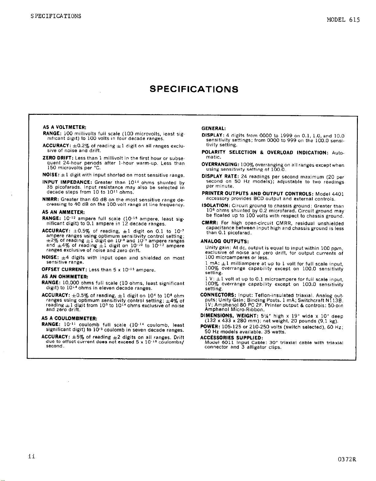
SPECIFICATIONS
AS A VOLTMETER:
RANGE:
ACCURACY: +0.290 of reading +1 digit on all ranges exclu.
ZERO DRIFT: Less than 1 millivolt in the first hour or subse-
NOISE: * 1 digit with input shorted on most sensitive range.
INPUT IMPEDANCE: Greater the” 10” phms shunted by
NMRR: Greater than 60 d8 on the most sensitive range de.
AS AN AMMETER:
RANGE: lo-‘2 ampere full scale (1O-L5 ampere, least sig.
ACCURACY: b-0.5% of reading,
NOISE: f-4 digits with input open and shielded on most
OFFSET CURRENT: Less than 5 x IO-l5 ampere
AS AN OHMMETER:
RANGE:
ACCURACY: &0.5% of reading.
AS A COULOMEMETER:
RANGE:
ACCURACY: +5% of reading 3~2 digits on all ranges. Drift
100
nificant digit) to 100 volts in four decade ranires.
sive of noise and drift.
quent 24.hour periods
150 mliCrOYOlt* pm “C.
35 picofarads. Input resistance may aIs0 be selected in
decade steps from 10 to 10” ohms.
creasing to 40 dB on the
nificant digit) to 0.1 ampere in 12 decade ranges.
ampere ranges using optimum sensitivity control setting;
*2% of reading *I digit 0n l@a and lo-3 ampere ranges
and 14% of reading *1 digit on
ranges exclusive of noise and zer0 drift.
sewitive range.
digit) to
ranges using optimum sensitivity control setting; *4% of
reading + 1 digit from
and zero drift.
millivolts full scale
10,000
ohms full scale
10” ohms
in
eleven
109 to 10’”
(100
microvolts.
least sig
after l.hour warmup. Less than
lOOwIt range at
-tl
line frequency.
digit
on 0.1 to l@’
1O-Lo to lo.‘1 ampere
(10
ohms. least significant
decade ranges.
hl
digit on
ohms exclusive pf noise
10’ to lOa ohm
10.” coulomb full sca1e (lo-” coulomb. least
significant digit) to 10’5coulomb in seven decade ranges.
due ta offset c”rrent does not exceed 5 x lO-‘I coulambs,
secpnd.
GENERAL:
DISPLAY: 4
sensftlwty
tivity setting.
POLARfTV SELECTION & OVERLOAD INDICATION: Auto-
matic.
OVERRANGING: lOO%overrangingon all ranges exceptwhen
“Sing Se”sltl”lty setting of 100.0.
DISPLAY RATE: 24 readings per second maximum (20 per
second on 50 Hz models); adjustable to tw, readings
per minute.
PRfNTER OUTPUTS AND OUTPUT CONTROLS: Model 4401
accessory provides BCD output and external cpntmls.
ISOLATION: Circuit ground to chassis ground: Greater than
IO6 ohms Shunted by 0.2 microfarad. Circuit ground may
be floated up to
CMRR: For high open-circuit CMRR. residual unshielded
capmtance between input high and chassis ground is less
than 0.1 picofarad.
ANALOG OUTPUTS:
Unity gain: At dc. Output is equal to input within 100 ppm.
exclusive of noise and zero drift. for Output currents of
100
1 mA: fl milliampere at up to 1 volt for full scale input,
100%
setting.
1 V: *l volt at
100% pverfange capability except M 100.0 sensitivity
setting.
CONNECTORS: Input: Tefkxvinsulated triaxial. Analog wt.
puts: Unity Gain: Binding Ppsts. 1 mA; Switchcraft Nl13B.
1V; Amphenol 80 PC 2F. Printer output &controls: 50.pin
Amphenol Micro-Ribbon.
DIMENSIONS, WEIGHT: 5%” high x
(132 x 433 x 280 mm); net weight. 20 pounds (9.1 kg).
POWER: 105.125 or 210.250 volts (switch selected), 60 HZ:
50 Hz models available. 35 watts.
ACCESSORIES SUPPLIED:
Made1 6011 Input Cable: 30” triaxiel cable with triaxial
connector and 3 alligator clips.
digits from 0000 to
settings; from 0000
100 volts
microamperes or fess.
overrange capability except on
up to 0.1 microampere for full scale input.
1999 on 0.1, 1.0,
to 999 on the 100.0 sensi-
with respect to chassis ground.
100.0
19”
wide Y 10” deep
and 10.0
sensitivity
ii
0372R
Page 3
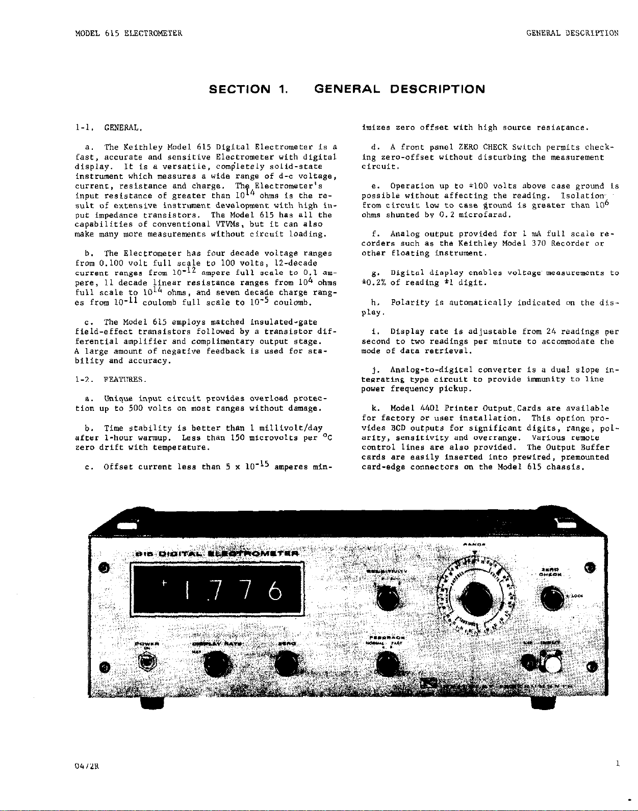
MODEL 615 ELECTROMETEX
SECTION 1.
l-l.
GENERAL.
a. The Keittlley Model 615 Digital Eleceromeeer is a
fast, accurate and sensitive Electrometer with digital
display.
instrument which measures a wide range of d-c voltage,
current, resistance and charge. Thy4Electrometer’s
input resistance of greater than 10 ohms is the result of extensive instrument development with high input impedance transistors. The Model 615 has all the
capabilities of conventional VTVMs, but it can also
make many more measurements without circuit loading.
b. The Electrometer has four decade voltage ranges
from 0.100 volt full scale to 100 volts, 12-decade
CUrrent ranges from 10-12 ampere full scale tcl 0.1 ampere, 11 decade linear resistance ranges from lo4 ohms
full scale to 1OL4 ohms, and seven decade charge rang-
es from lo-11 coulomb full scale to 1O-5 coulomb.
C. The Model 615 employs matched insulated-gate
field-effect ~ransiseors followed by a transistor differential amplifier and complimentary outpue stage.
A large amount of negative feedback is used for stabiliey and accuracy.
1-2. FEATURES.
a. Unique input circuit provides overload profec-
tion up eo 500 volts on most ranges without damage.
b. Time stability is better than 1 millivolt/day
after l-hour warmup. Less than 150 microvolts per ‘=C
zero drift with temperature.
C. Offset current less than 5 x 1O-L5 amperes min-
It is a versatile, comp’letely solid-state
GENERAL DESCRIPTION
imizes zero offset with high source resistance.
d. A front panel ZERO CHECK Switch permits check-
ing zero-offset without disturbing the tneasurement
CiX”iC.
e. Operarion up to *lOO voles above case ground is
possible without affecting the reading. Isolatio”~
from csrcuit low to case ground is greaeec than 106
ohms shunted by 0.2 microfarad.
f. Analog output provided for 1 mA full scale recorders such as the Keiehley Model 370 Recorder or
other floating instrument.
g. Digital display enables voltage’measurements to
l O.Z% of reading *I digit.
h. Polarity is automatically indicated on the dis-
Pk+,
i. Display rate 1s adjustable from 24 readings per
second to two readings per minute LO acconmadate the
mode of data retrieval.
j. Analog-to-digital converter is a dual slope intearaeing type circuit to pro”ide inaounity to line
power frequency pickup.
k. Model 4401 Printer Output.Cards are available
for factory or user installation. This option provides BCD outputs far significant digits, range, polarity, sensitivity and overrange. Various remaee
control lines are also provided. The Output Buffer
cards are easily inserted into prewired, premouneed
card-edge connectors an the Model 615 chassis.
04728
Page 4
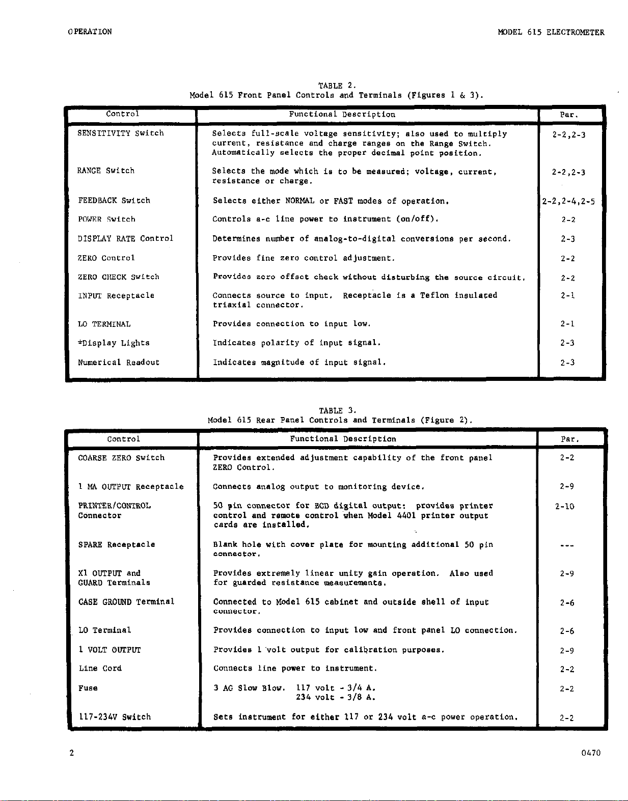
OPERATION
WDEL 615 ELECTROMETER
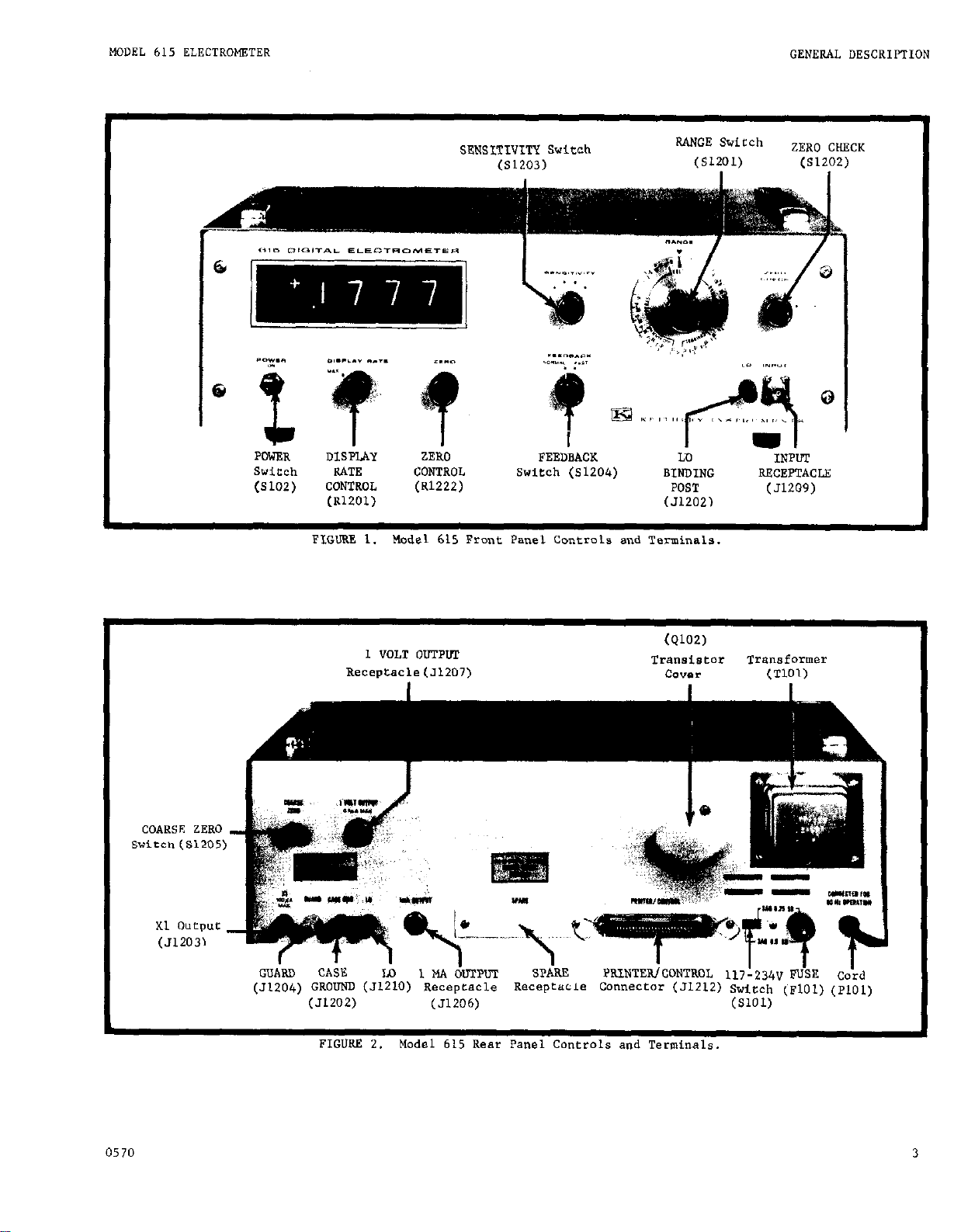
Model 615 Front Panel Controls and Terminals (Figures 1 & 3).
TABLE 2.
contra1 F”“ctio”*l Description
SENSITIVITY Switch
Selects full-ecsle voltage sensitivity; slso used to mulriply
current, resietance and charge ranges on the Range Switch.
Automatically eelecrs the proper decimal point position.
RANGE Switch
Selects the mode which ia to be measured: voltage, current,
resistance or cherge.
FEEDBACK Switch
POWER Switch
Selects either NORMAL or FAST modes of operation.
Controls e-c line power to instrument (an/off).
DISPLAY RATE Control Determines number of analog-to-digital conversions per second.
ZERO caner01 Provides fine zero control adJuseme”e.
ZERO CHECK Switch Provides zero offset check without disturbing the source circuit.
INPUT Receptacle
Connefts wurce to input. ~ecepeacle is a Teflon insulneed
triaxia1 connector.
LO
TERMINAL
*Display Lights
Numerical Readout
Provides connection to input low.
Indicates polarity of input signal.
Indicates magnitude of input signal.
Par.
2-2,2-3
Z-2,2-3
2-2,2-4,2-5
2-2
2-3
2-2
2-2
2-l
2-l
2-3
2-3
Control
COARSE ZERO Switch
1 MA OuTPuT Receptacle
PRINTER/CONTROL
CO”“eCtOC
SPARE Receptacle
Xl OUTPm and
G”m.tl Terminals
CASE
GROUND Terminal
LO Terminal
1 VOLT OWPIPI
Line Cord
F”M
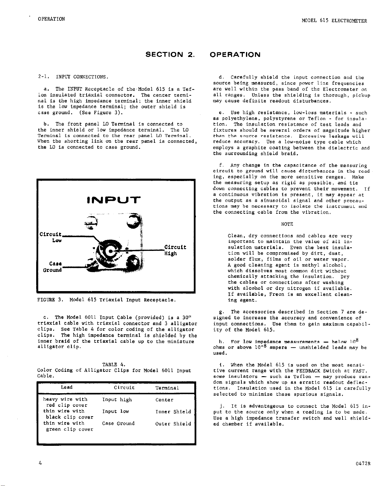
Model 615 Rear Panel Controls end Terminals (Figure 2).
TABLE 3.
Functional Description
Provides extended adfustment cepabflity of the front panel
ZERO Control.
Connect[i analog output to monitoring device.
50 pin connector for BCII digital output: provldea printer
control and remote control when Model 4401 printer ootput
cards ere installed.
Blank hole with cover plate for mounting edditional 50 pi”
CO”“BCtOC.
Provides extremely linear unity gsi” operation. Also used
for guerded reeFstance a.easureme”te.
Connected to Model 615 cabinet and outside shell of input
Connector.
Pravidea connection to input low end front panel LO connection.
Provides l’volt output for calibration purposes.
connecta line power to inatroment.
3
AD
Slow Blov.
117 volt - 314 A.
234 volt - 3/g A.
Psr.
2-2
2-9
2-10
__-
2-9
2-6
2-6
2-9
2-2
2-2
117-234V Switch Sets lnatrument for either 117 or 234 volt a-c power operation.
2-2
2 0470
Page 5
MODEL 615 ELECTROMETER
GENERAL DESCRIPTION
SENSITIVITY Switch
POWER DISFLAY
ZERO
Switch PATE CONTROL
(S102)
CONTROL (R1222)
(R1201)
FIGURE 1. Model 615 Front Panel Controls and Terminals.
(S1203)
FEEDBACK LD
Switch (S1204)
RANGE Switch
(51201)
BINDING
POST
(51202)
ZERO CHECK
(S1202)
INPUI
RECEPTACLE
(51209)
COARSE ZERO
switcn (S1205)
Xl ouepur
(51203)
1 VOLT ODTPW
Transistor
FIGURE 2. Model 615 Rear Panel Controls and Terminals.
(9102)
Transformer
0570
3
Page 6
OPERATION
MODEL 615 ELECTROMETER
SECTION 2.
2-l.
INPLPI CONNECTIONS.
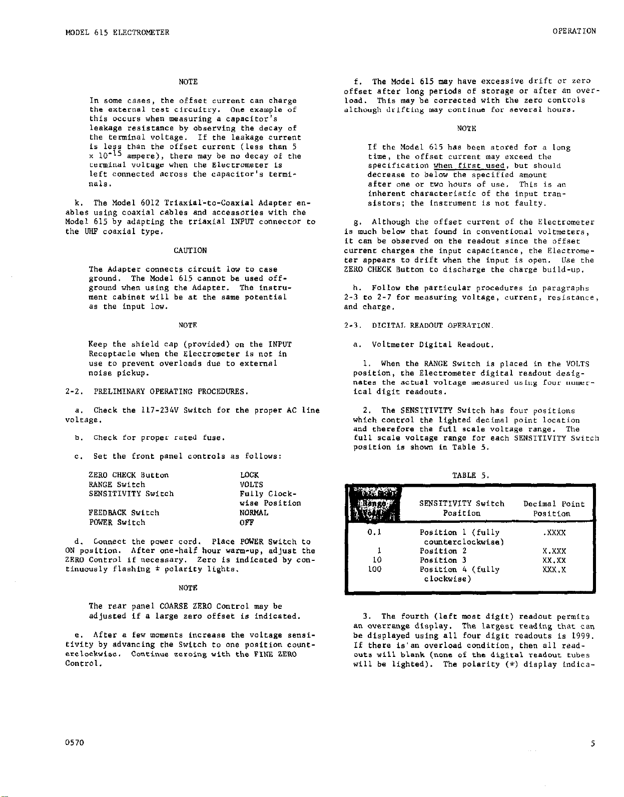
8. The INPUT Receptacle of the,Model 615 is a Teflon insulated triaxial connector. The center terminal is the high impedance terminal: the inner shield
is the low impedance terminal; the outer shield is
case ground.
b. The front panel LO Terminal is connected to
the inner shield or low impedance terminal. The LO
Terminal is connected to the rear panel LO Terminal.
When the shorting link o” the rear panel is connected,
the LO is connected to case ground.
(See Figure 3).
INPUT
OPERATION
d. Carefully shield the input connection and the
source being meaaured, since power line frequencies
are well within the pass band of the Electrometer o”
a11 ranges.
may cause definite readout
“se high resistance, low-loss materials - such
e.
as polyethylene, polystyrene or Teflon - for insula-
tion. The insulation resistance of test leads and
fixtures should be several orders of magnitude higher
than the source resistance. Excessive leakage will
reduce accuracy.
employs a graphite coating between the dielectric and
the surrounding shield braid.
f. Any change in the capacitance of the measuring
circuit to ground will cause disturbances in the read-
ing, especially on the more sensitive ranges. fake
the measuring setup a.s rigid as possible, and tie
down connecting cables to prevent their movement. If
a continuous vibration is present, it may appear at
the output as a sinusoidal signal and other precautions may be necessary to isolate the instrument and
the connecting cable from the vibration.
Unless the shielding is thorough, pickup
disturbances.
“se a law-noise type cable which
NOTE
FIGIRE 3. Model 615 Triaxial Input Receptacle.
c. The Model 6011 Input Cable (provided) is a 30”
triaxial cable with triaxial connector and 3 alligator
clips. See Table 4 far color coding of the alligator
clips.
The high impedance terminal is shielded by the
inner braid of the eriaxfal cable up to the miniature
alligator clip.
Color Coding of Alligator Clips for Model 6011 Input
TABLE 4.
Cable.
Lead
heavy wire with
Input
high
C*llt*r
red clip cover
thin wire with
Input low
Inner Shield
black clip cover
thin wire with Case Ground
Outer Shield
green clip cO”er
Clean, dry connections and cables are very
important to maintain the value of all insulation materials. Eve” the best insulation will be compromised by dirt, dust,
solder flux, films of ail or water vapor.
A good cleaning agent is methyl alcohol,
which dissolves most common dirvwithout
chemically attacking the insulation.
D=Y
the cables or connections after washing
with alcohol or dry nitrogen if available.
If available, Freon is a” excellent cleaning agent.
The
g.
accessories described in Section 7 are designed to increase the accuracy and convenience of
input connections. “se them to gain maximum
capabil-
ity of the Model 615.
h. Far low impedance measurements - below lo*
ohms or above 10-S ampere - unshielded leads may be
used.
i. When the Model 615 is used on the most sensitive ~“rrent range with the FEEDBACK Switch at FAST,
same insulators - such as Teflon - may produce random signals which show up as erratic readout deflec-
tions. Insulation used in the Model 615 is carefully
selected to minimize these spurious signals.
It is advantageous to connect the Model 615 in-
j.
put to the source only when a reading is to
be made.
“se a high impedance transfer switch and well shielded chamber if available.
4
04728
Page 7
MODEL 615 ELECTROMETER
OPERATION
NOTE
In some cases, the offset current can charge
the external test circuitry. One example of
this occurs when measuring a capacitor’s
leakage resistance by observing the decay of
the Germinal voltage. If the leakage current
is less than the offset c”rrent (less than 5
x lo-l5 ampere), there may be no decay of the
terminal voltage when the Electrometer is
left connected across the capacitor’s termi-
nals.
k. The Model 6012 Triaxial-to-Coaxial Adapter enables using coaxial cables and accessories with the
Model 615 by adapting the triaxial INPUT connector to
the UHF coaxial type,
CAUTION
The Adapter connect? circuit law to case
ground. The Model 615 cannot be used offground when using the Adapter. The instrument cabinet will be at the same potential
as the input law.
NOTE
Keep the shield cap (provided) on the INPUT
Receptacle when the Electrometer is not in
use co prevent overloads due to external
noise pickup.
2-2.
PKECMINARY
OPERATING
PROCEDURES.
f. The Model 615 may have excessive drift or zero
offset after long periods of storage or after an over-
load. This my be corrected with the zero controls
although drifting may continue for several hours.
NOTE
If the Model 615 has been stared for a long
time, the offset current may exceed the
specification when first
decrease to below the specified amo”nt
after one or two hours of “se.
inherent characteristic of the input transistors; the instrument is not faulty.
g. Although the offset current of the Electrometer
is much below that found in conventional voltmeters,
it cm be observed on the readout since the offset
currene charges the input capacitance, the Electrometer appears to drift when the input is open. Use the
ZERO CHECK Button to discharge the charge build-up,
h.
Follow the particular procedures in paragraphs
2-3 co 2-7 for measuring voltage, current, resistance,
and charge.
2-3. DIGITAL READOUT OPERATION.
a. Valtmecer Digital Readout.
1. When the RANGE Switch is placed in the VOLTS
position, ehe Electrometer digital readout designates the actual voltage measured using four numerical digit readouts.
used,
but should
This is an
a. Check the 117-234V Switch for the proper AC line
voltage.
b. Check for proper rated fuse.
See the front panel controls as follows:
C.
ZERO CHECK Button
RANGE Switch
SF.NSItI”ITY Switch
FEEDBACK Switch NORMAL
POWER Switch OFF
d. Connect the power cord. Place POWER Switch to
ON position.
ZERO Conerol if necessary. Zero is indicated by continuously flashing * polaricy lights.
The rear panel COARSE ZERO Control may be
adjusted if a large zero offset is indicated.
e. After a few moments increase the voltage sensitivity by advancing the Switch to one position CLIUIICerclockwiae.
Control.
After one-half hour warm-up, adjust the
NOTK
Continua zeroing with the FINE ZERO
wise- Position
2. The SENSITIVITY Switch has four positions
which control the lighted decimal point location
and therefore the full scale voltage range. The
full scale voltage range far each
position is shown in Table 5.
TABLE 5.
SENSITIVITY Switch
Position
I -~-
0.1 Positicm 1 (full”
1 1 Position Position
10 10 Position Position
100 100 PosFtFon PosFtFon
I I
3. The fourth (left most digit) readout permits
a.* averrange display. The largest reading that can
be displayed “sing all four digit readouts is 1999.
If there is’an overload condition, then all readouts will blank (none of the digital readout tubes
will be lighted).
counterclockwise) counterclockwise)
2 2 x.xXx x.xXx
3 3 xX.xX xX.xX
4 4 (fully (fully xXx.x xXx.x
clockwise) clockwise)
The polarity (*) display indica-
SENSITIVITY
Decimal Point
msi.cion
.xXxX
Switch
0570
5
Page 8
OPERATION
MODEL 615 ELECTROMETER
tars remain lighted during an overload condition
indicating the correct polarity. Thus the Electrometer display will indicate correctly within specifications with no ambFguous overload display.
4. To remove the overload condition, change the
SENSITIVITY Switch setting or decrease the input
signal magnitude.
b. Ammeter Digital Readout
1. When the RANGE Switch is placed in the AMMETER
position, the Electrometer digital readout desig-
nates the voltage across an accurately known selfcontained resistor. The RANGE Switch selects the
calibrated range resistor for current measurements
from 10-l to lo-11 amperes. The range resistor is
the reciprocal value of the Range setting. The
readout indicates the voltage across the Range resismr.
2. The full scale current range is determined by
multiplying the Range setting times the digital
readout display.
The SENSITIVITY Switch operates
in the same fashion aa for voltmeter measurements.
(Refer to preceding paragraph 2-3, a).
3. The full scale current range far various front
panel control settings is shown in Table 6.
TABLE 6.
ac~rately knovn capacitor since the Electrometer
is sensitive to the integral of the current applied
from the external unknown source.
2. The coulomb measurement is determined by mul-
tiplying the RANGE Switch setting times the digital
readout display.
e. DISPLAY RATE Control. (This control is a continuously variable control that permits the user to
select the rate of analog-to-digital conversion).
That is, the control determines the number of times
a new reading will be recomputed per unit of time.
Thts is useful for sampling a continuously varying inpllt current as well as for controlling slower external
devices such as paper tape punches and printers. With
the DISPIAY Control in the MAX Position the display
rate is 24 times per second (20 for 50 HZ models).
When the control is varied clockwise, the rate de-
creases to a minimum of about 2 per minute in the extreme clockwise position. The front panel DISPLAY
SATE Control applies to the digital circuitry only.
VOLTAGE MEASUREMENTS.
2-4.
a. The Model 615 can meas,,re an unknown voltage
when the low impedance terminal is up to 100 volts
off case ground. Safe operation of the Electrometer
is insured by grounding the case. To use the Model
615 for off ground voltage measurements, disconnect
the shorting link between LO and CASE GND Terminals
on rhe rear panel. (Refer t.3 Figure 2).
Full Scale RANGE SENSITIVITY I
Switch
C. Ohmmeter Readout.
1. When the RANGE Switch is placed in the OHMS
position, the Electromerer digital readout designates the actual voltage across the unknown resistor as an accurately known current (internal to the
Electrometer) is applied to the unknown.
2. The RANGE Switch selects the current for Olw
lll~ClS”C~lU~“t~.
The current is the reciprocal value
of the OHMS range setting from 105 to lo12 ohms.
The SENSITIVITY Switch operates in the same fashion
aa for voltmeter measurements.
3, The actual resistance measurement is deter-
mined by multiplying the RANGE Switch setting tFmes
the digital readout display.
d. Coulombmeter Readout.
1. When the RANGE Switch is placed in the CO”LO”BS position, the Electrometer digital readout
designates the actual voltage across a self-contained
CAUTION
Operating the Model 615 at more than 100
volts off ground may permanently damage
the instrument. The isolation between
circuit low and ground could break dawn
making the instrument unusable far safe
off ground measurements.
Refer to Paragraph 2-6 far complete instructions for
making off ground measurements.
b. The Model 615 has been designed to meas”re valt-
ages up to 100 volts from very high resistance sources.
However, the Model 615 can also be used for meaaurements from low sr,urce resistance and voltages up to 30
kilovolts with high voltage divider probe.
1, The input resistance can be decreased in or-
der to reduce the effects of stray pickup with low
sou*ce resistances.
Refer to Paragraph 2-4, f for
complete instructions.
2. ear measurements of voltage up to 30 kilovolts
refer to Paragraph 2-4, g which describes various
divider probes available from Keithley.
c. The Model 615 can measure voltages in two modes:
Normal Mode and Fast Mode.
1. Normal Mode.
In the Normal Mode - FEEDBACK
Switch at NOWAL - the unknown voltage is connected
to the INPW Receptacle. Input impedance with th
RANGE Switch in VOLTS position is greater than 10
84
ohms shunted by 35 picofarsds,
0570
Page 9
2. Fast Mode.
1" the fast Mude - FEEDBACK
Switch at FAST - the effects of inp"t cable capaci-
tance may be reduced for measurements fcum very high
source resistances. Guarded valtage measuremenr~
may aiso be made.
d. normal lode voltage Measurements
ZERO CHECK ButtOn LOCK
RANGE Switch
SENSITIVITY Switch
VOLTS
Fully Cluckwise
FEEDBACK Switch NORMAL
TO make aff graund measureme"zs, refer 'CO
Paragraph 2-6.
2. connect the Modei 6011 Trianial Input Cable
eo the unknown voltage as fallows:
a) the heavy wire with red clip cover should
be connected to the source high potential.
c) The thin wire wirhgrceaclip cover should
not be connecred when the shorting link between
LO end CASE Terminals on the rear panel is connected.
NOTE
To make off ground measurements. refer to
Paragraph 2-6.
3. ""lock the ZERO CHECK Button eo make a mea-
surement
4. Adjusr the SENSITIVITY Switch c~unrercL~ckwie.e
LO increase the Model 615 sensitivity. Readjust rhe
ZERO control as necessary after each change in sen-
sitivity.
5. The voltage measured is indicated directly 0"
the digital display with the decimal poinr automatically indicated. The poiarity is auLomatical,y
indicated corresponding CO Lhe potential of the
Electr~merer input high with respect to input low.
NOTE
The Model 615 has 100% overranging on all
ranges except for rhe 100 volt full range
sensitivity. An overload on any range is
indicated by a blanked digital display, a
feature which averts erroneous readings
when 200% of full range Is exceeded. The
digital display is Lighted when the over-
load is removed.
e. ~aat Mode voltage Measurements
1. set the frant panel controls as follows:
ZERO CHECK Butfc'n LOCK
RANGE Switch
SENSITIVITY SWitCh
FEEDBACK Switch
VOLTS
Fully Clockwise
FAST
0470
Page 10
OPERATION
2.
Model 6103A Divider Probe for measurements up
to 30
kilovolts. This probe permits meas”rements
with overall accuracy of Cg%.
1012
ohms maximum. The actual voltage is obtained
Input r**i*t**c* is
by multiplying the Electrometer digital display
times the divider ratio.
NOTE
The Model 6012 Triaxial-to-Coaxial Adapter
must be
used
with Models 6102A and 6103A
sF”ce tile probes are termFnated with a LW
connector. When using the Model 6012, the
case ground is connected to inp”t law so
that the Electrometer may not be used for
off ground measurements. -
2-5. CURRENT
MEASUREMENTS.
a. The Model 615 can measure an unknown current
when the low impedance terminal is up to 100 volts off
case ground. Safe operation of the Electrometer is
insured by grounding the case. To “se the Model 615
far off ground current measurements, disconnect the
shorting link between LO and CASE GND Terminals on the
rear panel. (Refer co Figure 2).
CAUTION
Operating the Model 615 at more than 100
volts off ground may permanently damage
the instrument. The isolation between
circuit low and ground could break down
making the instrument unusable for safe
off ground meawrements.
Refer to Paragraph 2-6 for complete instructions for
making off ground meas”eements.
b. The Model 615 can meas”re currents in two modes:
Normal Mode and Fat Mode.
1. Normal Mode.
eny renge
- the cwrent is determined by measuring
In the Normal Mode - used on
the voltage drop across a self-contained reeistor
shunting the electrometer amplifier input. This
method permits a minimum noise m~as”rement when re-
sponse speed is not.critical.
2. Fwt Mode.
I” the F.ast Mode - for “se only
MODEL 615 ELECTROMETER
below 10-S ampere range - a self contained resistor
is connected between the electrometer amplifier input and output (in the feedback loop). This method
permits faster response speed since the effect of
input capacitance is minimized. The input volcsge
drop is reduced to less than 100 microvolts on any
range. Refer to Table 7 for typical Response and
Noise performance for various values of input capacitance.
C. Normal Mode Current Measurements.
1. Set the front panel controls as follows:
ZERO CHECK nutron
LOCK
RANGE Switch 10-l AMPERES
SENSITIVITY Switch Fully Counterclock-
wise
FEEDBACK Switch NORMAL
NOTE
To
make off
ground measurements, refer to
Paragraph 2-6.
2. Connect the
Model 6011 Triaxial Input Cable
for meeauring s,, unknown current as follows.
a) The heavy wire with red clip cover should
be connected to the source high potential.
b) The thin wire with black clip cover should
be connected so as to place the Electrometer in
series with the c”rrent to be measured.
c) The thin wire with green
clip cover should
not be connected when the shorting link between
LO and CASE GND Terminals an the rear panel is
connected.
3.
Unlock the ZERO CHECK Button to make B mea-
surement.
4. Adjust the RANGE Switch to increase the Slec-
emmeter sa”siti”ity for CUrrent measurements.
5. The full range c”rrent for the Electrometer
is determined by multiplying the digital display
times the RANGE Switch setting. The best accuracy
for current meas”rements is obtained by “sing a
Typical Effects of External Inp”t Capacitance on Response Speed and Noise Performance in C”rre,,t Measurements
TABLE 7.
with the Model 615.
i-l****
$;to -
$"
10-S
10-7
10-6
s
Rise Time (seconds)
No C
2.0 2.0
.07 .45 .45 .07
,015 ,015
,003 .003
.003 ,003
2eE
5000pF
2.0 6 x lo-l5 1.5 x 10⁻¹⁴
.45' .07
,015 ;.i ;,m;l3 ;.":
,003
,003 3.3
No C
- x
8.5 x 10⁻¹⁴
Output
Noise
(Peak-Co-Peak)
$5;
s’x 10-11
x 10-10
5000pF
7 x 10-13
i.2 ;,!p;"
2
x 10-10
Page 11
MODEL 615
SENSITIVITY Switch seeting which permits the use of
the smallest value rage resistor. The rsnge resistor value is equivalent CO the reciprocal of the
RANGE Switch setting. The input voltage drop across
the shunt resistor is indicated directly on the
Electrometer digital display.
ELECTROMETER
NOTE
OPERATION
The ZEN, CHECK Sutt~” provides a short
across the feedback of the Electrometer
Amplifier to enable zero adjustment.
Do not apply a short circuit ecross the
Electrometer input terminals since this
will creete ““stable amplifier operation
The SENSITIVITY Switch settings permit sn
input voltage drop af O.i, 1, 10, and 100
volts for current measuremenfs in the
mrmsl Mode. on the LO-9 to 10-l’ AMPERES
settings of the RAN E Switch, the resistors
(109, 1010, and 101
age coefficient uf .O*% per vale (naminal).
1f the SENSITIVITY Switch is adjusted far a
100 v”lt input drop, then a” additional
error of 2% occurs for the current messure-
lS**t.
the smallest input drop possible to minimize
voltage coefficient errors.
d.
low 10-5 amperes).
1. Set the front panel controls es follows:
ZERO CHECK Button
RANGE Switch
SENSITIVITY Switch
FEEDBACK Switch
TO make aff graund measurements refer ta
Psragraph 2-6.
2.
for measuring an unknow” current ae in 2-5, c-2.
3. unlock the ZERO CHECK Sutton t” make e mee-
surement
‘rherefore ie is reconrmended t” select
Fast mde Current Weasurements (for current be-
Connect the Model 6011 Triaxial 1”put Cable
E
ohms) used have a volt-
LOCK
10-6 AMPERES
Fully Councerclock-
wise
FAST
NOTE
4. Adjust the RANGE Switch to increase the Slec-
tr”meCer seneitivity for current measurements.
5. The full range current for the Electrometer
is determined by multiplying the digital readout
times the RANGE Switch setting. The best accuracy
for current measurements is Obtained by using a
SENSITIVITY switch setting which permits the use of
the smallest value range resistor. The range cesist”r value is equivalent to the reciprocal of the
RANGE Switch settine. The input voltane drop, across
ehe shunt resistor Is indicated directly on the
EiectromeLer digital display.
NOTE
The source resistance of the circuit eo be
measured should not be Less than 0.1 rimes
the range resistar used since adequate
feedback voltage cannot be developed at the
input and zero stability is adversely affected. The range resistor is the reciprocal of the AMPERES range in ohms.
CAUTION
Foe measurement of capacitor leakage cur-
rents using the Pest Mode, a very
voltage supply must
pacitor connected across the input, the
electrometer is exCrem*ly sensitive to
voltage transients with a resultant in-
crease in readout noise.
be
used. With a ~a-
stable
I
I
I-
a-7
I 1
I
SOURCE I
L--------l L------------l
FIGURE 4.
0470 9
I I
I
: ME)WJ&NG I
I
1 = ’ readout
‘f
X
R+Ri”
Error Due to Ammeter Resistsnce.
I
I
I
1 readout
__ _ _ _
I
R
AMMETER
I
I
Page 12
OPERATION MODEL 615 ELECTROMETER
e. Galvanometric current Measurement Method.
I. operate the Electrometer in the Fast Mode as
described in Paragraph 2-5, d.
3. Adjust the Current Source co obtain a null on
the Electrometer digital readout. Increase the
Electrometer sensitivity as needed. The value of
the current which is suppressed is indicated o” the
current source setting.
NOTE
The connections for the Galvanometric Method
require the following accessories.
1 - Model 261 Current Source
1 - Model 6012 Adapter
1 - UHF tee fitting, Part No. cs-171
1 - Low noise coaxial cable, Model 2611
1 - Low noise coaxial cable, Part No. 19072C.
2-6.
OFF GROUND MEASUREMENTS.
a. ‘fhe Model 615
can be used for measurements when
the low impedance rerminal is up to IO0 volts off case
ground.
Safe operation of the Electrometer is insured
by grounding the case. To use the Model 615 for off
ground measurements, disconnect the shorting link between LO and CASE GNC Terminals a” the rear panel.
(Refer co Figure 2).
CAUTION
Operating the Model 615 at more than 100
volts off ground may permanently damage
the instrument. The isolation between
circuit low and ground could break down
making the instrument unusable for safe
off ground measurements.
b. Normal Mode Measurements. D‘sconnect the shorting link between LO and CASE GND Terminals on the rear
panel.
Connect the Model 615 case securely to earth
ground for maximum operator safety. Operate the Alectrometer 8s described in Paragraphs 2-4 or 2-5.
c. Fast Mode Measurements. Disconnect the shorting
link between LO and CASE CND Terminals on the rear
panel. Connect the Model 615 case securely eo earth
ground for maximum operator safety. Operate the Alectrometer as described in Paragraphs 2-4 or 2-5.
WARNING
The 1X4 analog outp”f can only be
used with
a recorder which will operate off ground
such as the Keithley Model 370.
NOTE
The
Model 615 ca”““t be operated off ground
if the Model 6012 Adapter is used since the
input Low and chassis ground are connected.
2-7. RESISTANCE MEASUREMENTS.
a. The Model 615 ca” be used to measure resistance
since the Electrometer permits accurate voltage or
current measurements from high resistance sources.
ResFstance can be
measured F” the following three ways.
1. Normal constant CurrenL Technique.
2.
Fast Constsne Current Technique.
3. Volt-Ammeter Method.
b. Normal Constant C”rre”t Resistance Measurement.
1. I” the constant current method, the Electrom-
eter meas”res the voltage drop across the unknown
resistance when a constant current is applied. The
voltage drop is the” proportional to the resistance
of the unknown.
2.
The Normal mode is recommended f r measure-
ments from 100 to 1O’l ohms. Above 10
Pl
ohms use
the Fast constant current technique.
10
0470
Page 13
MODEL 615 ELECTROMETER
OPERATION
3. Set the front panel controis as fallows:
ZERO CHECK SULLO” LOCK
RANGE Switch
SENSITI”ITY Switch
FEEDBACK switch NORMAL
1011 OHMS
Fully Counterclock-
wxse
4. Connect the unknown resistance between the
electrometer input high and low as for normal Mode
Voltage Measurements.
5. Unlock the ZERO CHECK Hutton to make a mea-
S”Tellle”t.
NOTE
Do nae open circuir the Electromeeer on the
OHMS ranges; the input will de”elop a large
voltage due to its constant currene charac-
teristic. Keep the input shorted or the
ZERO CHECK Button locked.
6. the unknown resistance is determined by multiplying the digital display times the RANGE twitch
setting. “se the smallest RANGE Swiech setting for
beBe possible accuracy.
7. The applied test voltage is indicated directly
on the digital display in volts.
8. The test current is the reciprocal of the OHMS
Range setting.
NOTE
2. set the front panel controls as follows:
ZERO CHECK Button LOCK
RANGE Switch 1011 OHMS
SENSITI”ICY SWFtch Fully Counterclock-
wise
FEEDBACK Switch FAST
3. connect the unknown resistance between the
Electrometer input high and GUARD Terminal as for
Fast Mode Voltage Measurements.
4. ““Lock the ZERO CHECK Button to make a mea-
SuremenL.
5. the unknown rcsisrance is determined by multi-
plying the digital display times the RANGE switch
setting.
6. The low terminal of the INPUT Receptacle is
now a driven guard.
It may be used t” minimize the
effects of capacity berween hi&h end low and errors
due to leakage reSiSta”ce between big,, and low.
7. The Model 6oLl Input Cable. supplied with the
Model 615, provides a convenient means of making
guarded reeistance meesurements. connect the shart-
in&t link between the CASE GRO”ND and GUARD Terminals
“n the rear panel. This allows the CASE GROUND ur
blue test lead terminal to be connected CO the Luw
impedance side of the unknown resistance.
me inner
shield or the black test clip is the GUARD Terminal.
d.
Volt-Ammeter Resistance Measurement (to 10’6
ohms).
Shield the input if the resistance sample
exceeds 108 ohms.
Fast COnSLant current Resistance Measurement.
(&ommended for 10” to 1ol4 ohms measurements).
1. The Fast Mode permits faster response speed
when measuring very high resistances.
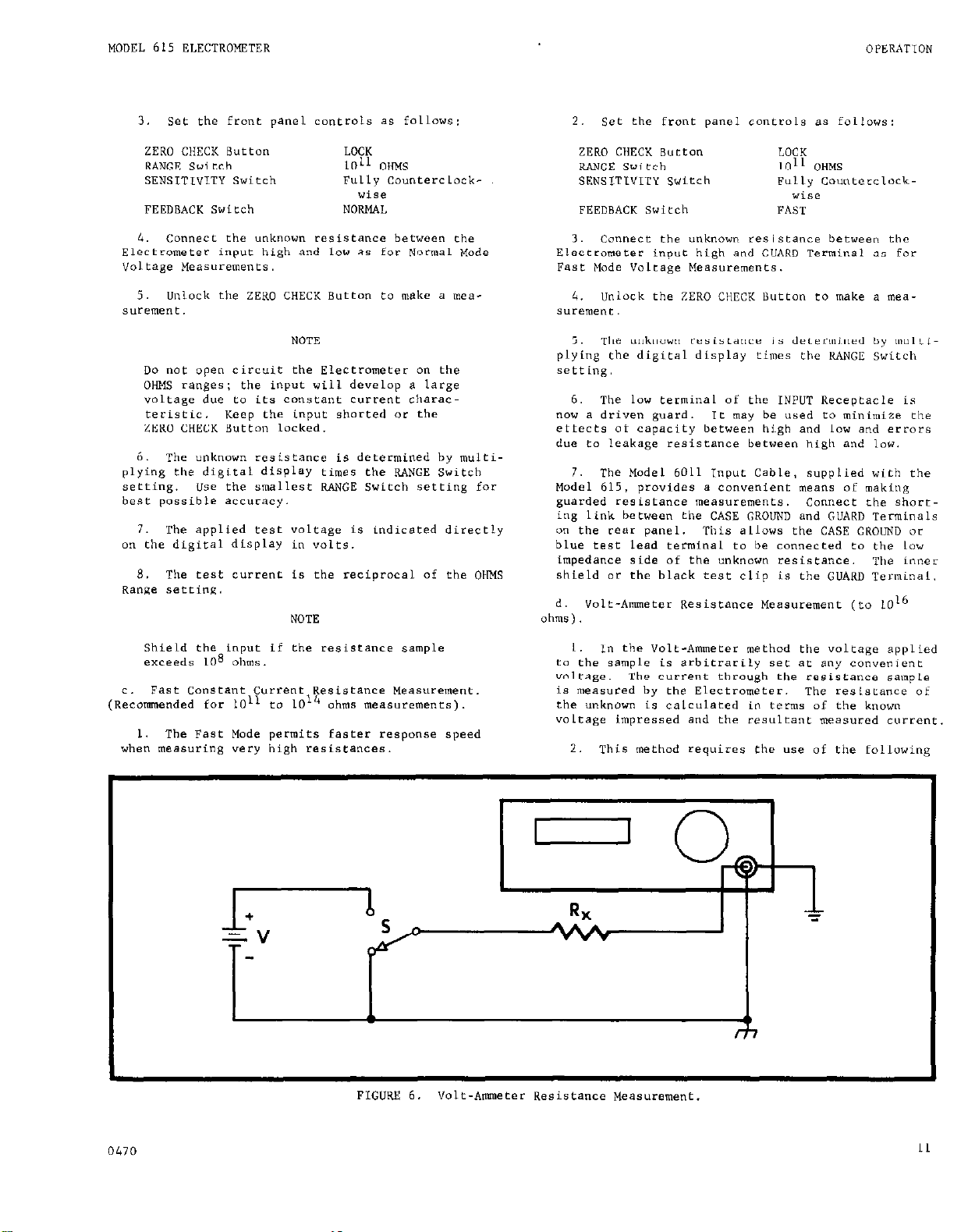
FIGURE 6. Volt-Ameter Resistance ,.,easuremenc.
1.
In the Volt-Ammeter method the voltage applied
to the sample is arbitrarily set at any cO”“enir”t
uoltage. The current through the resistance sa,“ple
is measured by the Electrometer. ‘rhe resistance of
the unknown is calculated in terms of the known
voltage impressed and the resultant measured current
2. This method requires the use of the folluwing
0470
11
Page 14
OPEP.ATION
MODEL 615 ELECTROMETER
instr”me”ts and *cc***0ri**.
1 - Voltage Source, such as Keithley Models
240A or 241.
1 - Shielded switch, such as Keithley Models
6104, 3011 or 4194.
1 - Test Cable, such as Model 6108
1 - Model 6012, “XF to Triax Adapter.
3. Connect the voltage source, switch, and uoknown resistance as shown in Figure 6. since the
~lecrrometer is used for the measuremene of current,
refer to Paragraph 2-5 for complete instructions.
NOTE
Refer to Paragraph 2-6 for complete instructions for meking off ground measurements.
4.
To make a eesistame measurement, place Switch
s in the “OFF” position 8s shown in Figure 6. Ad-
,,st the voltage source for a predetermined voltage.
Place Switch S in the “ON” position to
apply the
voltage ecross the unknown resistance. Allow a
iod of time for the current through the unknown re-
sistance to stabilize.
Unlock the ZERO CHECK Sutton
to take a current reading. Adjust the RANGE Switch
and SENSITIVITY Switch to obtain a satisfactory
reading.
5. After a reading is made. place the ZERO CHECK
Sutton to LOCK poeition and place Switch s to “OFF”
pOSiti”“.
Rem”“* the unknown resista”Ce and replace
with a second sample if necessary.
NOTE
If the voltage applied to the sample is not
100 times the Electrometer input drop, the”
the unknown resistance ia calculated es
follows:
R x = Vsource
- “Input oroe
lMeeasured
where Rx = ““known resistance,
VSource - Applied voltage,
“Input Drop
= Electrometer input voltage
drop
and l”easured = Current measured by Electrom-
eter.
2-8. CHARGE mASuP.EMmTS.
per-
Eq. 1
b. Set the front
ZERO CHECK Button
KANCE Switch
SENSITIVITY Switch
FEEDS.4CK switch
panel controls as
LOCK
10-7 COULOMBS
Fully Counterclock.
wise
FAST
follows:
c. Connect the Electrometer to the current eource
to be measured as described in Paragraph 2-5.
d. Unlock the ZERO CHECK Sutton to make B measure-
ment. Adjust the SENSITIVITY Switch to obtain a see-
isfactory reading.
changing the SENSITIVITY Switch
setting doea not affect the transfer of charge from
the source to Electrometer.
e. The coulombmeter reading is determined by mulciplying the digital display times the RANGE Switch
CO”LOMBS setting.
If the RANGE Switch must be changed
to obtain a satisfactory reading, repeat steps b, c.
and d above.
NOTE
The input offset current of the Electrometer
contributes a charge of 5 x IO-l5 coulomb
per second and should be subtracted from the
actual reading.
f. After a coulombmeter reading is made, discharge
the integrating capacitor in the Electrometer by
placing tile ZERO CHECK BUteon to I.OCK position.
Discharge capacitor for at lease 20 seconds on the IO-’
COULOMB range before making another measurement.
NOTE
For informeti”” concerning Static Charge
measurements, request the Product Note
entitled “Electrometer Stetic Charge
Measurements”. The Model 615 should be
used with Keithley Models 2501 end 2503
Static detector Probes for
Static
Charge
Meas”rements. 0” not sttempe to use the
Model 615 in the COULDMBS mode for Static
Charge meesuremeots since the Electrometer
is very sensitive to charge trensients.
2-9,
RECORDER OUTPUTS.
The Modal 615 provides several outputs for
1toring an a”al”g or dIgital signal. me “ario”
outputs are
summarized as follows.
~~.
a. Charge measurement or current integration can be
accomplished using the Model 615 in the coulombmeter
mode,
very accurate self-contained
eter output is
The electrometer indicates the voltage across a
capacitor. The Electrom-
therefore a voltage which is
propor-
tional to the integral of the applied curreot.
NOTE
For a more complete discussion of current
integration, request the Keithley Product
Note entitled “Using the Electrometer Voltmeter es a Current Integrating or Charge
Meas”ring I”sCr”ment.”
12
1. 1MA OUTPUT. This ““tpot provides a 1 milli-
ampere analog outpoe corresponding to a full range
itlP”C .
NOTE
The Keithley Model.370 may be conveniently
used to obtain a chart record with 1% Ii”earity. The Model 370 haa 10 speeds, re-
quires no preamp, and permits operation up
to *lOO volts off ground when used with
the Model 615.
A special
phone plug such
as Switchcraft S-290 must be used with the
Model 615.
0470
Page 15
OPERATION
2. 1 VOLT OlJTPLn.
analog output corresponding to a full range input.
The 1 VOLT OOTPW is useful for monitoring by oscil-
loscopes or voltmeters which will not load the ELectrometer output to exceed 0.1 microamperes. This
output is also used for calibration of the analag-
to-digital converter.
3. X1 OUTPUT (unity Cain). This output provides
a unity gain signal for applications requiring very
accurate measurements from high impedance sources.
The output is equal to input within 100 ppm at dc,
exclusive of noise and zero drift, for output cur--
rents of 100 microamperes or lees.
4. DIGITAL OuTPLm.
a complete description of the PRINTER/CONTROL connector and external controls.
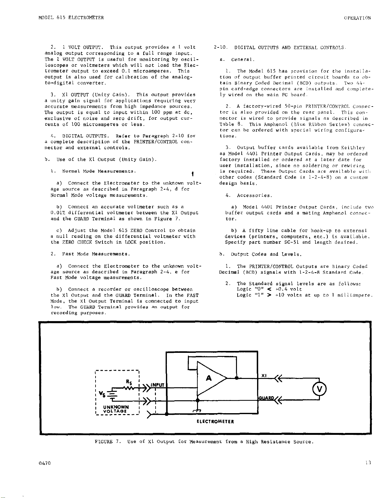
b. Use of the Xl Output (Unity Gain)
1. normal “ode ?.,eaeureme,,ts.
a) Connect the Electrometer to the unknown volcage source as described in Paragraph 2-4, d for
normal Mode voltage measuremeots.
b) Connect an *ccuraLe voltmeter such as a
0.01% differeneial voltmeter between the X1 Output buffer output cards and a mating Amphenol connecand the GUARD Terminal as shown in Figure 7.
This output provides a I vole
refer to Paragraph 2-10 for
a. General
1. The Model 615 has provision for the installation of output buffer printed circuit boards co obtein Sinary Coded Decimal (RCD) outputs. Two !+!apin card-edge connectors are installed and complecely wired on the main PC board.
2. A factory-wired 50-pin PRINTER/CONTROL cannectar is also provided on the rear panel.
nector is wired to provide signals as described in
Table 8. This Amphenol (RLue Ribbon Series) connec-
tar can be ordered with special wiring configure-
tions.
3. Output buffer cards available from Keithley
as Model 4401 Printer Output Cards. may be ordered
factory installed or ordered at a later date for
user installation, since no soldering or rewiring
is required. These Output Cards are available with
other codes (Standard Code is l-2-4-8) on a CIISC~I
design basis.
4. Accessories
a) Model 4401 Printer Output Cards. include two
tor.
Thik con-
c) Adjust the Model 615 ZERO Control to obtain
a null reading on the differential voltmeter with
the ZERO CHECK Switch in LOCK position.
2. Fast Mode MeasuremenLs b. Output Codes and Levels.
a) Connecr the Electrometer to the unknown volt-
age source ee described in Paragraph 2-4, e for
Fast Mode voltage measucements.
b) Connect a recorder or oscilloscope between
the x1 Output and the GUARD Terminal. In the FAST
Mode, the XI Output Terminal is connected to input
low. The GUARD Terminal provides an output for
recording purposes.
b) A fifty line cable for hook-up to external
devices (printers, computers, etc.) is avaiLable.
Specify part number SC-51 and length desired.
1. me PRINTER/CONTROL outputs are i3inary Coded
Oecimsl (SCO) signals with l-2-4-8 Standard code.
2. The Standard signsl levels are as follows:
Logic “0” < co.4 volt
Logic “1” > *lO volts at up to 1 milliampere.
-
0470
FIcUwi 7. Use of xl Output for Measurement from a High Resistance Source.
I 3
Page 16
OPERATION
MODEL 615 ELECTROMETER
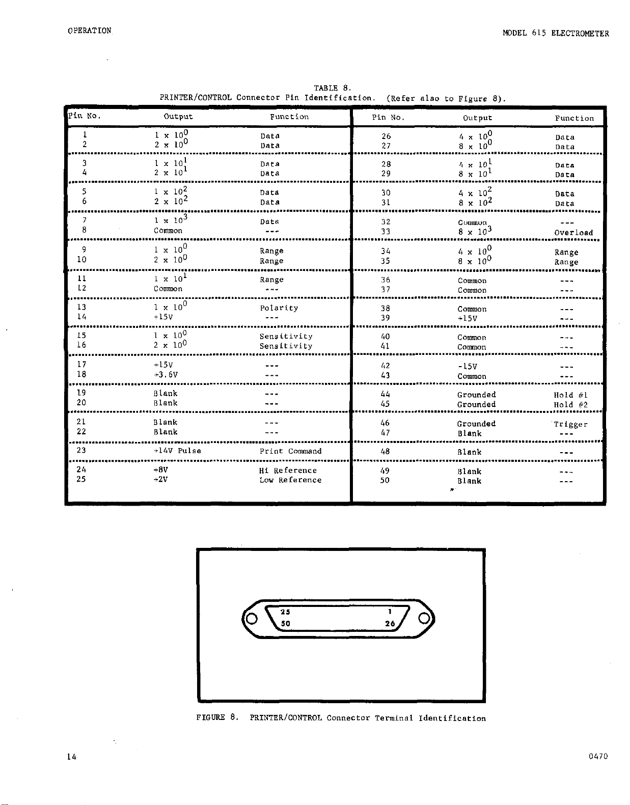
PRINTER/CONTROL Connector Pin Identification.
.n NO.
1
2
,........................................................ . . . . . . . . . * . . . . . . . . . . . . . . . .
3
4
,...................................................................................
5 1 x
6
,................................ * . . . . . . . . . . . . . . . . . . . . . . . . . . . . e . . . . . . . . . . . . . . . . . . . . . II . . . . . . . . . . . . . . . . . . . . . . . . . . . . . . . . . . . . . . . . . . . . . . . . . . . . . . . . . . . . m . . . . . . . . . . . . .
7
8
. . . . . . . . . . . . . . . . . . . . . . . . . . . . . . . . . . . . . . . . . . . . . . . . . . . . . . . . . . . . . . . . . . . . . . . . . . . . . . . . . . . .
9
10 2 x 100
. . . . . . . . . . . . . . . . . . . . . . . . . . . . . . . . . . . . . . . . . . . . . . . . . . . . . . . . . . . . . . . . . . . . . . . . . . . . . . . . . . . .
11 1 x 101
!.f . . . . . . . . . . . . . . . . . . . . . . . . . . . . . . . . . . . . . . . . . . . . . . . . . . . . . . . . . . . . . . . . . . . . . . . . . . . . . . . .
13
14
. . . . . . . . . . . . . . . . . . . . . . . . T!.?Y . . . . . . . . . . . . . . . . . . . . . . . . . . . . . . . . . . . . . . . . . . . . . . . . . . . . . .
15
16
, . . . . . . . . . . . . . . . . . . . . . . . . . . . . . . . . . . . . . . . . . . . . . . . . . . . . . . . . . . . . . . . . . . . . . . . . . . . . . . . . . . .
17
18 +3.6V
, . . . . . . . . . . . . . . . . . . . . . . . . . . . . . . . . . . . . . . . . . . . . . . . . . . . . . . . . . . . . . . . . . . . . . . . . . . . . . . . . . . .
19 Blank
20 Blank
. . . . . . . . . . . . . . . . . . . . . . . . . . . . . . . . . . . . . . . . . . . . . . . . . . . . . . . . . . . . . . . . . . . . . . . . . . . . . . . . . . .
21 Blank
22
. . . . . . . . . . . . . . . ..*............-....................................................
23 114” Pulse
. . . . . . . . . . . . . . . . . . . . . . . . . . . . . . . . . . . . . . . . . * . . . . . . . . . . . . ..*...........................
24 +BV
25 +2v
omput Function
1 x 100
2 x 100
1 x 101
2 x 101
102
2 x 10²
1 x 10³
COllllllO”
1 x 100
oata
“ata
“ata 28 4 x 101
mea
oaca 30
oata
oata
__-
Range 34
Range 35 8 x 100
Range
COlllUlO”
1 x 100
1 x 100
2 x 100
t15v
---
m*arity 38
___
sensitivity
Se”Siti”ity 41
__-
--___
_-_
Blank
___
Print Command
Hi Reference
LOW Reference 50
I
. . . . . . . . . ‘.” . . . . . . . . . . . . . . . . . . . . . . :.I...? . . . . . . . . . . . . . . . . . . . . “.“..r.” . . . . . . .
. . . . . . . . . 2 . . . . . . . . . . . . . . . . . . . . . .8..x.!.? . . . . . . . . . . . . . . . . . . . . D.2.” . . . . . .
. . . . . . . . . . . . . . ..*...................... * . . . . . . . . . . . . . . . . . . . . . . . . ..........
. . . . . . . . . . . . . . . . . . . . . . . . . . . . . . . . . . . . . . . . . . . . . . . . . . . . . . . . . . . . , . . . . . . . . . . ..,
. . . . . . . . . i.:. . . . . . . . . . . . . . . . . . . ..~~~.! . . . . . . . . . . . . . . . . ...... :.I .......,
. . . . . . . . . 3: . . . . . . . . . . . . . . . . . . . . . t!” . . . . . . . . . . . . . . . . ......... :.:.-. ......,
. . . . . . . . . . . . . . . . . . . . . . . . . . . . . . . . . . . . . . . . . . . . . . . . . . . . . . . . . . . . . . . . . . . . . . . . . .
. . . . . . . . . . . . . . . . . . . . . . . . . . . . . . . . . . . . . . . . . . . . . . . . . . . . . . . . . . . . . . . . . . . . . . . . . .
. . . . . . . . . . . . . . . . . . . e . . . . . . . . . . . . . . . . . . . . . .................................
. . . . . . . . . . . . . . . . . . . . . . . . . . . . . . . . . . . . . . . . . . . . . . . . . . . . . . . . . . . . . . . . . . . . . . . . . I
. . . . . . . . . . . . . . . . . . . . . . . . . . . . . . . . . . . . . . . . . . . . . . . . . . . . . . . . . . . . . . . . . . . . . .... .
(Refer also to Figure 8).
Pi” NO. *UtD”t F”“Cei”n
27
8 x 10 oata
OBCB
4 x 10²
31
32
8 x 10²
COlll!llO”
33 8 x 10³
4x 100
oata
oata
___
Overload
Range
Range
COUXllO”
40
common
COllllllO”
42
-15v
43 cammon
44 Grounded
45 Grounded
46 Grounded
47
Blank
48 Blank
49
Blank
Blank
d
___
-_-
-__
--___
Hold i/l
“old $2
‘Trigger
---
-__
--_
___
TABLE 8.
14
FIGURE 8.
PRINTER/CONTROL Connector
Terminal
Identification
0470
Page 17
MODEL 615 ELECTROMETER
OPERATION
C. output Information.
TABLE 9.
Model 4401 minter outpue Cards.
Model 4401 Printer Output Cards:
Provide BC,, output and external Control of Model 615; may be
purchased installed or separately for field installation (no wiring required).
minter outputs: BC” positive output represents
each of the four digits, exponene, sensieivity,
polarity and overrange. Standard code is l-2-4-
“0” < co.4 volt; “1” z 110 volts at up to
8.
one milliampere: o=oooo.
Print Commnd: Positive pulse of 14 volts from
a zzoo-ohm source with 1 volt per microsecond
rise time, 100 microseconds minimum pulse width.
print co,,ms”d give” after each A LO D conversion.
Renwte Controls:
Hold iii: Closure to ground inhibits A to D co”version, ac that instant.
Hold ,12: Closure to ground inhibits A to D co”version after reading has bee” completed.
trigger: Closure to ground initiates one conversion when in Hold 02. Integraeion period stares
8.3 ms (10 ma on 50-Hz models) after “Trigger”
or release of Hold 82.
connector: 50-p<* Amphenol Micro-Ribbon mou”Led
an Model 615. O”fp”t macing connector supplied
with 4401.
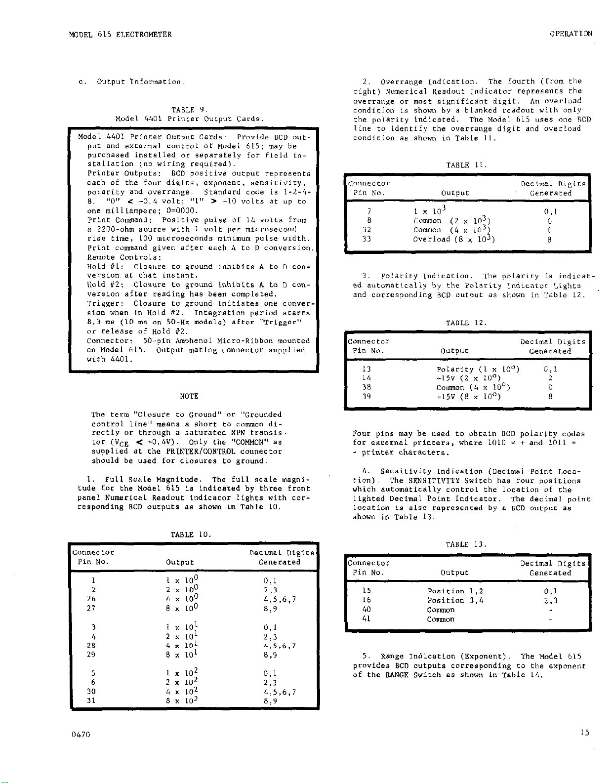
2. Overrange Indication.
The fourth (from the
right) Numerical Readout Indicatar represmts the
overrange or m”se significant digit. A” overload
candieia” is shown by a blanked readout with “nly
the polarity indicared. The Model 615 uses one RCD
line to identify ehe overrange digit and overload
condicio” as sham in Table 11.
‘TABLE 11
I
33 32
8 7
Overload C”olm”” Comma”
1 x 10³
(2 (4 (8 x x x 103) 103) 103)
O,l
0 0 8
3. mlarity IndicaLio”. The poiaricy is indicated automatically by the Polarity Iadicator Lighfs
and corresponding BCD output as show” in Table i?.
TABLE 12
OUtoUt
oecima1 Digits
Generated I
NOTE
The term “Closure to Ground” or “Grounded
control line” means a shore to common directly or through a saturated NPN eransistar (VcE < c0.N). Only the “COMMON” as
supplied at the PRINTER/CONTROL co”“ector
should be used for claaures to ground.
1. Full Scale Magnitude. The full scale magni-
tude for the ~“del 615 is indicated by three front
panel Numerical Readout indicamr lights with corresponding RCD outputs as show” in Table 10.
TABLE 10.
3 1 x 101
4 2 x 101
28 4 x 101
29 8 x 101
5 1 x 10²
6 2 x 10²
30 4 Y 102
31 8 x 10²
O,l
2,3
4,5x6,7
8.9
0.1
2,3
4>5,6,7
829
I
38 14
13
39 +15v common
Polarity
+15v (2 (8 (4 x x
(1
x 100) 100) x W)
100) 0,1
0 2 8
Four pins may be used to obcai” BCD polarity codes
*or external printers, where 1010 = + and 1011 =
- printer characters.
4. 8ensiei”ity Indication (mcimal Point coca-
Lion). The
SENSITI”ITY
Switch has four positions
which automarically control the locaeio” of the
lighted Decimal Point Indicator. The decimal point
location is also represented by a BCD outpue as
sham i” Table 13.
TABLE 13
Decimal Digits
OutpUt
Position 1.2
Position 3,4
COIIEW”
C~lmM”
5. Range Indication (Exponent). The Model 615
provides BCD outputs corresponding LO ehe exponent
of the RANGE Switch 88 show” in Table 14.
Generated
I
I
0470
15
Page 18
OPERATION
I
0470
TABLE 14
MODEL 615 ELECTROMETER
b) A” external device ca” also be used for
mester control such 8s a high speed printer.
Connector
Pin NO. Output
I
9
10
34
35
11
12
36
37
The print-out of the RANGE switch expanent uses 2
coluums to represent information far exponents from
00 thru 12. The exponent must be interpreted as
positive or negative depending on the parameter (amperes, coulombs, or ohms).
6. The ““de1 615 with Model 4401 Printer Output
Cards also provides ee,,wte control commanda for ex-
ternal devices. These commands are described fully
in Paragraph 2-10, d.
7. Examples of e typical printer output for various Model 615 readings are show” t” Table 15. In
the examples the p=<ntl”S davice 1s assumad to co”-
tain fonts of digits 0
columns ere needed to print all date.
1 x 100
2 v Exponent
4 x 100
8 x
1 x Exponent 031
COUSIIO”
COUSUO”
Common
Exponent 021
100
Exponent
100
Exponent 899
101
to
9.
Decimal Digits
Generated
223
495,637
In this case, eight
c) A completely independent “master clack” can
I
be used for system control for maximum flexibility.
3. Description Of external controls.
a) “HOLD 1”. This control inhibits A to D co”-
version at the instant a closure to Sraund is
made. The conversion cycle will =esume inmediate-
ly when the “HOLD 1” line is opened.
“HOLD 2”. This control inhibits A ta D con-
b)
version after a complete reading cycle. Further
conversions are inhibited as long as a closure to
ground is made. The c”“ve=slo” cycle will resume
immediately when the “HOLD 2” line is opened.
c) “TRIGGER”. This control initiates one com-
plete conversion when “HOLD 2” line is grounded.
Closure to ground may be momentsry or any longer
duration to initiate a conversion.
d)
“PRINT
positi”* going pulse of 14 volts after a complete
A to D conversion is made end all data line out-
puts are final readings.
Power Supply Voltages. The PRINTER/CONTROL
4.
Connector also provides p”we= supply u”ltaSes of
+15, -15, and ~3.6 valta as shown in Table 16.
COMMAND”. This control provides a
d. External Control.
1. To obtain optimum system performance, it is
often desirable to operate the Model 615 synchron““sly with other digital equipment, such a8 printers,
paper tape punches, computers and other data handling
devices. The Model 615 with 4401 Printer Cards installed provides several printer control commands for
the purpose of synchronizing external equipment to
schieva maximum conversion rates.
Several alternate approaches may be used in de-
2.
signing the overall system control scheme.
a) The Model 615 can be used to provide maste=
control of external devices so that the maximum
possible conversion rates ca” be obtained.
Front Panel
Diaital Readout
+0.275
+1.347
-086.4
-(blank)
+(hla”kj
+oo.oo
-.1632
+19.99
Range Switch
setting Polarity E Digit 6. Overlosd I
1O-5 AMPERES +
109 OHMS
VOLTS 0
lo-l1 AMPERES
VOLTS
VOLTS 1 632 0 00 -. 1632 volts
10-7 AMPF,RBS
+
+
+ 1
Significant ;
i
i
!
TABLE 16
Maximum
VOltaRe ‘aed Current
I
+3.6V
+15v
-15V
r
5. High and Low Reference. The PRINTER/CONTROL
Connector provides tw” Reference Voltages, High
(+SV) and Low (c2V). These levels may be used to
define the “HIGH” and “LOW” digital output states
for‘ external printing or computer devices.
TABLE 15.
Msg. i sells. i mp. I”t*CpC*t~tiLW
0 ! !
1 i 347 1 09 +1.347 x lo9 amp ohms
0
275 1 05 +.2?5 x 10⁻⁵
F 864
: 000 - . 11 averlaad 10-7 COULOMBS .i : negstive +
: 000
i
:
f
1
i
;
000 1 2
i
999 j 2 E 07 +19.99 x 10⁻⁷ amp
+50 In4
Cl0 mA 14,17,39
-10 IsA
i Renge
I
3
- 07
00 -R6.4 volts
positive overload
00 +oo.oo volts
I
Pin
18
42
No.
I
I
16
Page 19
MODEL 615
ELECTROMETER
OPERATION
a. Summary of oigital Outputs and Controls.
1. Standard Output Codes and Levels.
The stend-
ard output code for Model 4401 Printer Output Cards
is 1-2-4-S binary Coded Decimsl (&Xl). A binary
coded decimal digit is represented by a four-bit
binary code as shown in Table 17.
a) The “ON” state is defined as en output grearer then +10 voles into a resistance load of 10 kilohms or greater.
b) The “OFF” stete is defined a9 en outPut less
than co.4 volts.
TABLE 17.
Decimal
Number 4 bit
0 0
1 0
? 0
3
4
5
6
7
8
9
0 0
0
0
0
0
1
1 0 0
3 bit 2 bit
0
0 0
0 1
0
1
1
1
I
1
0
0
0
1
1
0
1 bit
L
c) Refer to Figure 19 for e circuit diagram of
the Model 4401 Standard Printer Output buffer
stage.
the “TRIGGER” command inLtiac*s one complete
conversion cycle. A second conversion will fol-
law only if the TRIGGER cormwind is removed and
re-applied a second time. The maximum conversion rate uslng.an external trigger is 24 readings per second.
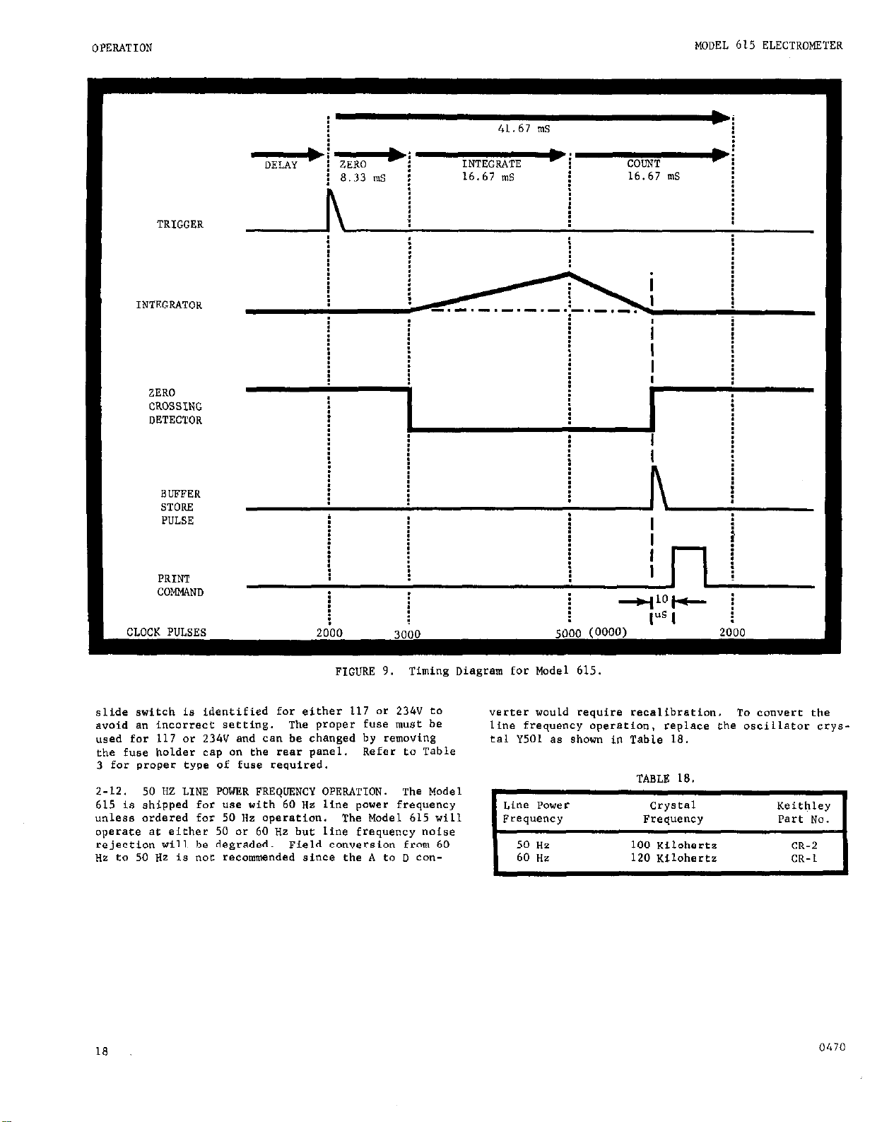
b) Conversion Cycle Timing. The Conversion
Cycle is composed of three timing periods, namely,
Integrator Zero, Integrator Sampling, and A-D
mounting period.
9.
P
1.
integrator Zero Period (ZERO). When a
Refer fo Timing Diagram Figure
trigger pulse initiates a new conversion cycle,
the Integrator circuit is zeroed for e period
not to exceed 8.33 miilisecands for 60 SC operation. (The Integrator Zero Period is 10.00
milliseconds for 50 Hz operation).
2. Integrator Sampling Period (INTEGIUTE).
0
1
0
1
0
1
0
1
0
1
The Integrator Sampling Period follows automac-
ically the Integrator Zero Period and lasts for
a duration of 16.67 milliseconds for 60 HZ operation. The Integrator Sampling Period Lasts
for a duration of 20.00 milliseconds for 50 ilz
0 pa L ;,ioyil.
*..
3. ‘A-D Counting Period (COUNT). The A-D
Counting Period is initiated immediately follow-
ing the Incegraeor Sampling Period. The actual
counting time duration will depend on the actual
integrator voltage up to a maximum of 2000 clock
pulses or 16.67 milliseconds.
Following the
counting period a Buffer/Storage command is
auromefically generated in order to store the
new reading in the output registers.
2. PRINTER/CONTROL Connector. The PRINTER/CONTROL
Connector used an the Model 615 provides for connec-
tions to 50 pins es Shown in
Table
8. The mating
connector supplied with Model 4401 is an Amphenol
Part Number 57-30500 or Keithley Part Number CS-220,
available on specie1 order.
3. Analog-to-Digital Conversion Cycle.
a) The analog-to-digital conversion cycle can
be initiated in any one of three ways.
1. DISPLAY RATE Control Set at MAX. With the
DISPLAY RATE Control set at MAX, cbe end of one
complete conversion triggers e second conversion
to obtain the maximum conversion rate of 24 readings per second.
2. DISPLAY RATE Control Set at Other Than MAX.
With the DISPLAY RATE Control set et some posi-
tion other than MAX, (uncalibrated control set-
ting) the end of one complete conversion triggers
a second conversion which is delayed by a speci-
fic time interval (DELAY). The time delay is a
function of the position of a continuously’variable control to provide a conversion rate from
24 readings per second to 2 readings per minute.
3.
‘71OI.D 2” With TRIGGER Control. With the
“HOLD 2” command grounded, a closure to~ground of
4. PRINT COMMAND. The PRINT COMMAND signal
is used to trigger external printers or paper
tape punches. The PRINT COMMAND signal is delayed 10 microseconds to allow the storage legisters to settle.
The PRINT COMMAND pulse width
is approximately 100 microseconds with e 1 voltl
microsecond rise time into a 1 kilohm load. The
pulse amplitude is approximated by the following
equation:
e, = 14~/(~+2200).
Eq. 2
where R ia the outpat load resistor.
The “OFF” state is less then +0.4 volt with ap-
proximately 1 milliampere sink current.
NOTE
The date stared in the Output Registers will
not change for et least 25 milliseconds for
60 HZ operation.
If the front panel controls are changed, the Sensitivity or Range
SCD output may be effected.
2-11. 117-234V LINE POWER OPERATION.
The Model 615
is shipped for use with 117” e-c line power unless
ordered for 234V operation. To convert eny instrument
for either 117” or 234V operation, use a screwdriver
to set the 117-234” Switch an the reer panel. The
0470
17
Page 20
OPERATION
MODEL 615 ELECTROMETER
INTEGRATOR
ZERO
CROSSING
DETECTOR
SUFFER
STORE
PULSE
41.67 ms
INTEGRATE
16.67 mS
COUNT
16.67 Ins
:-I--
bi
ei
l
PRINT
COMMAND
CLOCK PULSES
slide switch is identified for either 117 or 234V co
avoid an incorrect sectinS. The proper fuse must be
used far 117 or 234V and can be changed by
the fuse holder cap on the rear panel. Refer to Table
3 for proper type of fuse require*.
Z-12.
615
unless ordered for 50 Hz operation. The Model 615 will
operate at either 50 or 60
reJection will be degraded. Field conversion from 60
Hz eo 50 Hz is not recommended since the A to D con-
50 HZ LINE
is shipped for use with 60 Hz line power frequency
POWER FREQUENCY OPERATION. The Model
2000
FIGURE
Hz but line frequency noise
3000
9.
Timing Diagram for Model 615.
removing
.^
5000 (~OOU)
verter would require recalibration. TO co”“erc the
line frequency operation. replace the oscillator ccystal Y501 as shown in Table 18.
2000
18
0470
Page 21
XODEL 615 ELECTROMETER
CIRCUIT DESCRIPTION
SECTION 3.
3-l. GENE&U..
a. The Keithley Model 615 Digital Electrometer con-
SiSe.3 of t&m separate sections (except for the power
supplies) packaged rogeeber in one chassis for optimum
performance and convenience:
analog-to-digital converter.
b. The Electrometer is basically an extremely stable and linear DC voltmeter with a full-scale sensitir;‘y of 100 millivolts and an input impedance of
10 ohms shunted by 35 picafarads. sy using the
frone panel controls, shunr resiseors and capacitors
are selected to make measurements over a total of 120
voltage, current, resistance, and coulomb rariges.
Current and resistance are measured using precision
resistance standards, from 10 ohm wirewound resistors
to 1011 ohm glass-sealed, deposited carbon resistors.
Coulombs are measured using close tolerance polysty-
rene film capacitor standards.
the analog-to-digital converter is a dual slope
c.
integrating type converter with medium conversion
rate, cold cathode readout tubes, BCD outpue options
and external control.
3-2. ELECTF.omTER A!4PLIFIER OeEP.ATION.
a. The Model 615 electrometer amplifier employs
matched insulated-gate field-effect transistor8 fol-
lowed by a transis;or differential amplifier with a
high-voltage complementary output stage. Refer to
an Electrometer and an
CIRCUIT DESCRIPTION
Figure 10 which shows a block diagram of the Electrometer.
b. The Electrometer amplifier is connected as a
unity-gain, voltage-to-current converter configuration. Refer to Figure 11 for a simplified diagram of
the unity-gain amplifier in the Normal Mode. The
sensitivity selection circuitry is arranged such that
a full-scale input voltage (ei) results in a 1 rnilliampere output current through the Sensitivity resistor represented by Rs.
(es) is determined as follows:
The unity-gain voltage output
e, = ei .&
where K is the amplifier loop gain.
3-3. AMPLIFIER CIRCUIT
a. The amplifier input stage is a pair of insulatedgate field-effect rzr~nsistors (IGFET) designated 01201
and ~1202 connected in B differential configuration.
The “gate” terminal of transistor Q1202 is connected
eo the unity-gain output.
b. The input stage is followed by a Cransistor differential amplifier composed of transistors Q1203 and
Q1204. Transistors 01207 and 01212 make UP a bizh
&in stage which pre;ents “fold-we+ and ;‘lock-;p”
with positive input overloads. Diode D1214 between
0472R
19
Page 22
CIRC”IT DESCRIPTION
INPUT- , 4x1
,
A
ei
(P-Q!
MODEL 615 ELECTROMETER
\
f
is
FIGURE II.
base and emitter of transistor Q1209 prevents “fold-
over”
and
“lock-up” under negative input overloada.
NOTE
Amplifier “fold-over” is defined 88 a co”-
dieion where the i”sfrumenL erroneously
Indicates an on scale reading with a large
overload.
an amplifier stage saturates.
c. Frequency compensation is provided by capacitors
Cl213 and C1214, resistors R1240 and R1241, and cepacieor c1215.
trolled frequency response characteristic to insure
stability under all condicians of input end output capncieance loading.
d. The complementary-output stage composed of transisters Q1210 and Ql211 is connected co the unity-gain
output to complete the unity-gain amplifier clrcult.
e. The power supplies which provide *120 volts dc
for the output transistor atsge are floating with respect to chassis ground. The *9v power auppliea for
the amplifier gain stages are referred to the unitygain output.
“Lock-up” is a condition where
The compensation networks provide a con-
""lty-Gain Amplifier
g. The analog output signal for recorder outputs is
derived from a resistor divider network represented by
resistor RD in Figure 10.
1. 1 VOLT OUTPUT (51207). This output is derived
from the 1 milliampere current (for full scale inputs) which flows through a,resistor network of
1010.1 ohms. This output has been designed co provide a reference voltage for the analog-to-digital
converter. The 1 VOLT OUTPUT Terminal may be used
for monitoring purpose where loading ca” be 0.1 mi-
croampere maximum.
2. 1 MA OUTPUT (51206). This output provides a
one milliampere dc current for a full scale input
voltage of 100 millivolts, 1 volt, 10 volts, or 100
volts depending on the SENSITIVITY Switch setting.
The output cannectar used is a Witchcraft N113S female phone jack which connects ehe output in series
with the reference voleege divider RD.
3. Xl OUTPUT (51203). This output is the unitygain output as shown in Figure 11. The ~1 Output
provides a voltage es which is equal to ehe input
according Co the following ratio.
f. The SENSITIVITY Switch S1203 selects a resistor
network (represented by resistor Rs) to provide full
scale input ranges from 100 millivolts to 100 “Olts in
four steps. The output voltage to current conve’rsio”
is determined as follows:
sq. 4
20
where K is the amplifier loop gain.
3-4. AMMETER OPERATION.
a. Normal Mode. With the FEEDBACK Switch in the
0470
Page 23
CIRCUIT DESCRIPTION
NORMAL position, a* accurately known RANGE Swirch re~istor (CURRENT Range only) RI202 through R1212 is
connected in shunt across the Electrometer amplifier
input
Refer eo Figure 10 for a block diagram of the
Electrometer. The amplifier measures rhe voltage drop
across he Range resistor to determine the input current. The digital readout display and analog outputs
are calibrated to indicate the magnitude and polarity
of the voltage. The actual current is obtained by mul-
tiplying the readout times the current range selected.
b. Fast Node. With the FEEDBACK Switch in the
FAST position, an accurately known RANGE Switch resis-
tor (CURRENT Range only) R1202 through RI212 is con-
nected across the amplifier feedback Loop as shown in
Figure 12. The unity-gain output (Xl) is connected to
Input LO.
be used for monitoring purposes.
In this mode the GUARD and X1 Terminals may
The Fast Mode con-
ciguration minimizes the slowing effects Of input capacitance. The input voltage drop is maintained at
less than 100 micravalcs.
sistore are R1202 through F.1212.
c. Normal Mode Operation. When the FEEDBACK Switch
is in rhe NORMAL position, the unknown resistor is
connected between the INPUT high and low as described
in the OPERATTON section of this manual. The actual
resistance is determined by multiplying the digital
readour display times the OHMS Range selected.
The analog-to-digital converter circuit des-
cription can be found in paragraph 3-7.
This circuitry is separate from the analog
circuitry and is located on individual
printed circuit boards.
0470
Page 24
CIRCUIT DESCRIPTION
1VOLT OUTPUT
INPUT ,
22
> I
I
C
+ ,,
I\
I
I
I
0
Y
m
0
+
::RO
<GUARD
vo
FIGURE 14. Coulombmeter Fast Made.
0470
Page 25
MODEL 615 CIRCUIT DESCRIPTION
I
*II’1
. ! ! ! !
I I I I I I I
I I I I
I I I
I
0671
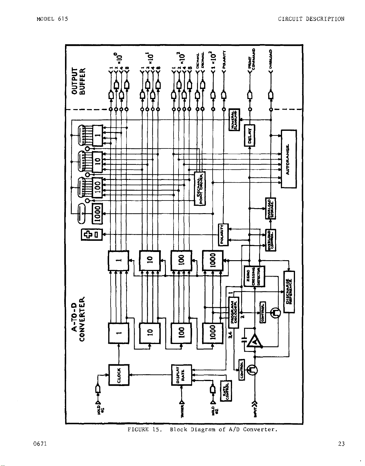
FIGURE 15.
Block Diagram ot
AID Converter.
23
Page 26

a. General (refer to Figure 15 for a detailed block
i------------------L--,
diagram of the A-to-D cO”“erter). The analog-to-dig-
ital converter operates using a dual slope integration
technique which has inherent line frequency noise rejection. The *“*log sign*1 is applied t” the integrator for one complete line frequency cycle, therefore
integrating the line frequency noise. me analog signal is the” remove* from the integrator input. The
voltage on the integraeor is then driven to zero to
complete the voltage-to-time conversion. The time interval to reach a “zero crossing” is counted and displayed on the “Readaut” in praportio” e” the origi”al
analog sign*,. The sequence is then repeated for a
second reading. (Refer to the Timing Diagram shown
in Figure 9).
b. The A-m-D converter is composed of nine major
circuits which perform the analog-to-digital conversions an* provide Various control commands.
1. Oscillator or clock
2. BCD counter
3. Delay Hold
b. Program/Decoder
5. I”tegr*tOr
6. Nero Crossing Detector
7. Buffer/Storage Register
8. Decoder/Driver
9. Numerical Readouf.
C. Oscillator or Clock.
pulses at a rate of 120 kilohertz for Electrometer
using 60 HZ line power. (The 50 HZ units have B pulse
race of 100 kilohertz).
The Oscillator produces
or “ntil Trigger is shorted to ground. After con“ersio”, ehe instrument will again be inhibited at
the beginning af ehe period (2).
3. If both Switches s1 an* s2 are clased, rile
conversion cycle works in the foliuwing manner.
a) After the previous converSion ihas been cm-
pleted, etle leading edge of the program comma**
(2) resets the flip-flop. I” this new con*icim
q is high and, therefore. the clock gives 110 output.
b) At that rime,
its cycle and, after the appropriate time. produces a pulse LhaL sets the flip-flap. This
changes g to a law state and a new C”n”erSio,l
cycle begins. After the reading has bee” corn-
pleted, the (2) camman* again resets the Elip-
flop and the timer again issues a “ew pulse co
set the flip-flop.
the ““ijunction timer begins
i.EW
H -
I I
d. BCD Counter. The BCD COULI~BT‘ counts the Clock
pulses with a total range of 5000 co”“cs. The Counter
ia composed of 4 i”di”idual counters designated 1, 10,
100, and 1000.
1. The “I”, “IO”, and “100” counters have a ca-
pacity of ten co”“ts each.
3. The tot*1 capacity of all four co”“ters is
5000 counts.
e, Delay Hold. The Delay Hold circuit controls the
DISPLAY RATE function and external Hold and Trigger
colmnan*a (refer eo Figure 16).
1t determines the length of time between A-ta-
1.
D conversions when the front panel DISPLAY RATE Control is Bet to any position other charI MAX. me
clock is stopped ac the beginning of the ZERO (2)
period for a time
DISPLAY RATE Control.
It ensures chat when the Hold 2 is grounded
2.
the conversion in process will be cornpIeced and new
data will be stored in the m,t,,ut storage register.
Then the clack will be inhibited at the beginning of
the ZERO period (2). The instrument will remain in
this condition indefinitely until Hold 2 is released
determined
by the rotation of the
Program/Decoder. The Program/Decoder circuit
e.
produces evenr commands to cantrol the overall se-
quence of events for a complete A-to-D conversian.
Integrator. The 1ntegraeor circuit operation is
8.
composed of three periods (refer to Figure 9).
I. zero Period. luring this period the intcgra-
tar amplifier is zeroed by ehe closure of s~itcll Sb.
Switches S,, s,, an* s* *IYe open to prevent integru-
tar charging (refer eo Figure 17).
2.
Integration Period. During this period,
switch Sb, SC, and Sd are open. Switch s, is closed
to permit charging by the analog voleage for a per-
24
0410
Page 27

FIGURE 17. rntegrator Block Diagram
h. zeru crossing Detector. me zero crossing De-
tector circuit provides a “High” or “Low” level output
depending on the polarity of the detected input. me-
Eer to Table 19 for a description of voitage outputs
of Lhe Zero Crossing detector (refer co figure 18).
Zero Crossing Detector Outpur Levels.
M N
0” -0.5” i1.5”
I
0”
I
i.
Buffer/Storage register. The ~ufferl~torage
Register is composed of “flip-flops” arranged to copy
the states of the various BCD counters.
Storage Register requires a Buffer Store command be-
fore any information can be transferred. The “flipflop” circuits provide coded information for Decoder/
Driver and the BCD outputs.
~j. Decoder/Dri.ver. The Decoder/Driver circuit de-
0470
TABLE 19.
13.5”
B
0”
c
ov
~1.5”
The BUf fer/
I
Page 28

MODEL 615 ELECTROMETER
CIRCUIT DESCRIPTION
TABLE 20.
I
comnan*
I
Function
ZERO
324
I
tor is charged by the analog signal for a period “f
1 line cycle or 16.67 milliseconds.
signal is remove* an* the integrator output is
driven co zero by e reference current. The Zero
Crossing Detector senses a zero crossing of the In-
eegreeor output an* remOweS the refeeence current.
The
The +1.5 vole levels are provided for control of the
Integrator an* Polarity storage Register. A pu1ae
command is also produced to initiate a Buffer/Store
and print Command output.
Suffer/Storage Register copies the SCD Counterstatea
et that instant of time.
in the Register is then available for the Decoder/
Driver an* external printout.
output and drives the numerical Readout for a digital display.
Model 4401 Buffer Card “utput~ in the form of posi-
cive (+lO volt) true logic (1-2-4-S BCD Code).
10.
Counter reaches 2000 counts and the Program/Decoder
provides a “2” commend to initiate a new conversion
cycle.
11. The Unijunction Timing Circuit will initiate
the ZERO period after a preset time delay controlled
by the front panel DISPLAY RATE Control.
3-S. AN.4Loc-TO-DIGrt*L CONVERTER CIRCD~TRY.
a. General. The circuits described in this eecti””
at-e located on the various Sub-Assemblies listed below
end in Table 22 of Section 4.
b. Oscillator Board.
portions of three circuits:
circuit, the Delay/Hold circuit, and the DischargeVoltage current source CirCUlt.
0:1
5. When the “3,4” comnlan* is given, the integra-
6. When the “O,l” command is given, the analog
detector provides outputs as shown in Table 19.
7. When the Buffer/Store command is given, the
8. The Decoder/Driver decodee the Buffer/Storage
9. The BCD output information is available at the
The conversion cycle is completed when the SCD
1. Oscillator Board, PC-217.
2. Integrator Board, PC-246.
3. Display/overload Board, PC-241
4. Readout Board, X-229
Polarity Board, PC-207
5.
6. output Buffer Board, PC-2L8
7. output Buffer Board, PC-209
1. Oscillator Cic’cuit. Trensi~tor Q501, crystal
I
The SCD coded information
The Oscillaeor Board codtains
INTEGRATE
COUNT
the Oscillator (clock)
~501, and phase shift capacitors C501, and C502 form
a “colpitts” type oscillator. Capacitors ~503 and
~504 are used for trimming the oscillator frequency.
I
I
The ““Cput is taken from the collector of transistor
Q510 which is a comnon emitter gain stage used for
squaring ee ““tpllt. Transistor Q507 serves as an
emitter-follower to reduce output impedance.
2. Delay/Hold Circuit. There ace three major
components in the Delay/Hold circuit: en “RS” type
flip-flop circuit, a ‘Wnijunction” timing circuit
an* a “ROld” gate circuit.
“RS” Type Flip-Flop
=)
gates the output of the clock depending on the
inputs at pins R and S. The RS flip-flop is coostrucced of gates QA5OlB and QA5OlC. The pins
are identified as shown in Figure 16.
“Unijunction” Timing Circuit. The unijunc-
b)
tion timing circuit determines the time delay
tween conversion cycles to obtain the
version rate 88 determined by the front panel DISPLAY RATE Control. The circuit is composed of
tran9isCors Q513 and Q514, timing capacitor C507,
and timing resistors ~532 end R1269 (DISPLAY RATE
Caner01 potentiometer located on the front panel).
c) “HOLD” Gate Circuit. (Refer to Figure 16
for identification of switches S1 and S2). The
“HOLD” gate circuit is composed of gates QASOlA.
QA501D, and QA502 (A, 8, C, and D). Switch S1 is
gate QA501A and is controlled by either the “HOLD
2” exrernal line or the “MAX” position on the
DISPLAY RATE Control.
Q513 which is controlled by either ebe “Q” output
of the flip-flop or the “HOLD 2” external line.
The “HOLD I” circuit is composed of gates QASOZS
and QA502C.
3. Discharge-Voltage Current Source Circuit.
The positive current source composed of tran~ierors
Q502 and Q506 delivers a constant current of +7.5
milliamperes tb drive a g-volt zener diode D602
(located on the Integrator Board, PC-246) when +REF
Terminal (Pin 13) is greater than co.7 volt. The
negative current ~““rce composed of erensistors Q508
and Q509 delivers a constant current of -7.5 milli-
amperes to drive a 9-volt zener diode 0601 (also
located on the Integrator Board, ~-246).
Integrator Board. The Integrator Board consists
c.
“f two ma,or circuits:
Zero Crossing Detector circuit.
1. Integrator Circuit. (Refer to Figure 17 for
identification of switches Sa, Sb, S,, and Sd). The
operation of the Integrator is controlled by ehe
poSitionS of switches So, Sb, S,, and Sd. switch
S, is transistor Q605. Switch Sb is transistor
Q606. Transistors Q601 through Q604 are control
circuits arranged e” turn off the proper FET Switchee
depending on the signals at pins 11 and 12. The in-
tegrator smplifier conslets of transistors Q607 and
~608 and ineegraced circuit QA601. The feedback ca-
pacitor is C603. Switches SC and Sd (located on the
Oscillator Board, PC-217) control the current for
‘)-volt zener diodes 0601 an* 0602.
Circuit.
Switch S2 is transistor
the Integrator circuit and the
The flip-flop
be-
desired coo-
~e~iseors ~602
26
0470
Page 29

CIRCUIT DESCRIPTION
MODEL 615 ELECTROMETER
through P.611 are full-scale calibration resistors.
2. Zero Crossing Detector Circuit.
(Refer to
Figure 18). The high gain amplifier is composed of
cascaded amplifiers Q~602 and qA603.
justment network consists of resistors
R648, R649,
and ~650. and diodes D6ii and 0612.
The zero ad-
~645, Rb46,
Transistor ~609 and other components form a 6-volt
supply for QA603 and the zero circuit. The Level-
splitter circuit consists of diodes D613 and D614,
resistors
~65L, ~652,
and R653 and gatee QA604 (A,
USC).
d. Display/Overload Board. The Display/Overload
Board conrains a BCD Counter (“1000” counter), a Program Decoder circuit, a”d a” Overload Control circuit.
1. The BCD Counter is composed of “J-K” flip-flop
circuits QA301 and
2.
The Program Decoder circuit is composed of
gates
QA303C
QA3048, QA304C, QA304D, QA305A, QA3058, QA305C.
QA305D, QA303E, QA306A, QA3068,
2
Commands).
3.
The Overload Control circuit provides a” over-
QA302.
and QA303D (3.4 Command) and QA304A,
and QA306C (0,L. &
load signal if a zero crossing does “ot occur in the
Discharge Period (0,L). 1t controls the Numerical
Blanking circuit end provides a” Overload Print sig*al.
e. Readout Board. The Readout Board contains Dec-
ade Counter circuits, Buffer Storage circuits, and me-
coder Driver and Di.splay circuits.
1. Decade Counter Circuits. Each decade counter
is composed af four J-K flip-flops. Circuits QA401
through ~A406 are Dual J-K FLip-Flop integrated circuits.
gate QA204A.
The -REF Control signal is determined
by QA202A, QA203A, QA2038, QA2028, OA202C, QA2”3C,
QA203D,
and QA2048.
4. Buffer Store
Command
Circuit. me Buffer
Store command is provided by J-K flip QA20111 and
gates
QA204C
and QA207A.
5. Overload Blanking Circuit. A portion of the
Overload
Blanking circuit QA204D. QA206R, and QA207B
is located on the Polarity Board. The remainder of
the circuit is Located a” the Display/Overload Board.
E-241.
g. output Buffer Board. PC-2LS. This board con-
tains
L5
buffer circuits to provide BCD Data and Overload and Polarity Print signals. Buffer circuits “A”
through “P” consist of transistor buffer stages PS
shown in Figure
19.
h. Output Suffer Board, R-209. ‘This board contains
six buffer circuits and various gate circuirs to provide Prinf Command and Range Signal PrinL signals.
1. Suffer Circuits.
Buffer circuits “*” through
“E” provide SC0 Range information.
2.
Print Command Circuits.
Suffer circuits com-
posed of transistors QllOi, Q1102, Q1104, Q1105.
41106,
and Q1107 provide Print Command signals as
determined by gaeee QAllOl (A,B,C, and D) and QALLO~
(A,t.C, and D).
3. Range signal Circuit. Transistors QllOS,
~21109, and QlllO comprise a Range Signal Buffer
stage controlled by the Lange Signal.
-
2.
Buffer Storage Circuits. The Buffer Storage
register is composed of Dual J-K Flip-Flop integrated
circuits QA409 through QA41k.
3.
Decoder Driver Circuits. QA415, QA416, and
QA417 ere Decimal Decoder Driver integrated cfrcuits.
4. Display CFrcuFts.
V4OL, “402, end “403 are
Readout Tubes for Units, Tens, and Hundreds respectively.
f. Polarity Board. The Polarity Board conteins
various circuits which are controlled by signals “6”
end “C” from the Zero Crossing Detector signal as
shown in Figure 18.
1. Polarity Indicator Control Cixc”it. This circuit drives the Polarity Indicator DS201 LO provide
a Polarity display. QAZOIA and QA206A are J-K Flip-
Flop circuits which conrroi transistors Q201 and 4202
2.
Polarity PrinC Signal Circuit. The Polarity
Print signal is determined by the q output of J-K
flip-flop QA206A.
3.
Discharge voltage Polerity Control Circuit.
The +REF Control signel is determined by QAZOlA and
0470
FIGURE 19.
Model 4401 Suffer Stage.
27
Page 30

CIRCUIT DESCRIPTION
MODEL 615 ELECTROMETER
4. Reference Voltages. A High and LOW Reference
voltage is provided by resistor divider R1114, R1115,
and R1116. The voltages are +8 volts (High) and +2
volts (Low).
POWER SUPPLIES (refer ea Schematic Diagram
3-9.
24044E).
a. *15 vole Supply.
1. The 115 volt supplies tap a-c power from a
secondary of transformer T101. Diodes 0103, D105,
0107
and
0108 and capacitors CL04 and Cl05 compose
a full-wave rectifier with filtering.
2. Transistors Q114 and Q115 form a differential
amplifier which compares the voltage at R115 with
the voltage of zener diode 0110. The difference
voltage is amplified by transistor Q109 and fed to
Darlington transistor pair, Q106 and Q107, which
series regulate the oueput voltage.
3. Transistors Q116 and 4117 form a differential
amplifier which compares the voltage ae R123 with
respect to la. The difference voltage is amplified
‘by transistor Q113 and fed to Darlington transistor
pair, QllO and Qlll, which series regulate the -15
volt aueput.
4. Transismrs Q108 and Q112 limit rhe output
current to about 200 milliamperes.
b. t3.6 Volt Supply.
1. The ~3.6 volt supply taps a-c power from a
secondary of transformer TlOl.. Diodes DlOl and D102
2nd capacitor Cl01 form a full-wave rectifier with
filtering.
2. Transismr 4105 amplifies the difference between the ~3.6 volt output and a reference voltage
derived from the ~15 vole supply and determined by
resistors R103 and R104. The difference voltage is
amplified by rraneistor Q104 which drives a Darling-
ton tmnsistor pair, QlOl and Q102. The Darlingto”
pair series regulares the +3.6 volt output.
3. Transismr 4103 limits the output current to
about 3 amperes.
C.
+170 Volt Supply.
1. The +170” supply taps a-c power from a second-
ary of transformer T101.
Diode Dill and capacitor
Cl12 farm a half-wave rectifier with filtering.
2. Transistor Ql19 amplifies the voltage develaped by the resistor divider RUE and R129. The
output of Q119 controls the series regulator cransistar Q118 to maintain the +170 volt output.
3. When the electrometer is overloaded, and overload signal drives transistor Q120 which in turn
controls the voltage at the base of transistor Q119.
The circuit composed of diode D112, transistor Q120,
and resistors R130, R131 and RI32 reduces the +I70
volt output to +80 voles when overloading occurs.
Grounding the overload input turns off transistor
Q120 causing diode 0112 to conduct and drive Q119.
4. The reduced +80 volt output causes blanking an
all Numerical Readout Tubes connected co the +170
volt supply.
t210 volt output. The t210 volt supply is an
d.
unregulated voltage supply using the, half-wave fil-
tered voltage at diode Dlll and capacitor C112.
e. “9
Volt
Supplies (shown an Schematic 24267E)
1. The *9 “olt supplies tap a-c power from a sacondary of transformer T1201 or T101. Diodes 01201
to D1204 and capacitors Cl216 and Cl217 for a full-
wave rectifier with filtering.
2. Zener diodes 01205 to 01208 provide regulated
*9 volt outputs.
f. 1120 “0lC Supplies.
I. The 1120 volt supplies cap a-c power from a
secondary of transformer T1201.
Diodes D1211 and
D1212 and capacitors Cl218 and Cl219 form a halfwe.ve rectifier with filtering.
2. Zener diodes 01209 and 01210 provide regulated
-rl20 vole outputs.
28
0470
Page 31

MODEL 615 ELECTROMETER REPLACEABLE PARTS
SECTION 4. REPLACEABLE PARTS
4-1. REPLACEABLE PARTS LIST. This section contains (Code Number), Manufacturer Part Number, and the
a list of components used in the Model 615 Digital
Electrometer for user reference. The Replaceable erence Number where applicable. The complete name and
Parts List describes the individual parts giving Cir- address of the Manufacturers is listed in Table 24.
cuit Designation, Description, Suggested Manufacturer (Refer also to Table 21 for Abbreviations and Symbols).
Keithley Part Number. Alsa included is a Figure Ref-
Abbreviations and Svmbols
A
Cb”aC
CerD
Cer Trimmer
CO”lP
DCb
Desig.
EAl
ET8
ETT
ELECTRICAL SCHEMATICS AND DUCRA”S. Schematics
4-2.
and diagrams are included to describe the electrical
circuits as described in Section 3.
which identifies all schematic part numbers included.
4-3. WOW TO “SE THE REPLACEABLE PARTS LIST. This
Parts List is arranged such that ehe individual types
of components are listed in alphabetical order.
perts for the instrument’s Main Chassis are listed
fallowed by printed circuit boards and other subassem-
blies. Refer to Table 23 for listing of circuit des-
ignacion series assigned to each major sub-assembly.
4-4. HOW TO ORDER PARTS.
a. Replaceable parts may be ordered through the
Sales Service Department, Keithley Instruments, Inc.
ampere
Carbon Variable
Ceramic Disc
Ceramic Trimmer
Camposition
Deposited Carbon
Designation
Electrolytic, Aluminum
Electralytic, tubular
Electrolytic, tantalum
Refer co Table 22
TABLE 21.
F farad
Fig.
GCb Glass enclased Carbon
k
u
M
Mfg.
MU
MY
NO.
The
Figure
kilo (103)
micro (10-6)
Meg (106)
Manufacturer
Metal Film
MYhC
Number
or your nearest Keithley representaeive.
b. When ordering parts, include the following in-
formation.
1. Instrument Part Number
2. Instrument Serial Number
Part Description
3.
4. Schematic Circuit Designation
5. Keiehley Part Number.
C. All parts listed are maintained in Keiehley
Spare Parts Stack. Any part not listed can be made
available upan request. Parts identified by the
Keithley Manufacturing Code Number 80164 should be
ordered directly from Keithley Instruments, Inc.
0.
P
PC
POly
Ref.
V
w
ww
W&V*=
OhIn
pico (to-121
Printed Circuit
Polystyrene
Reference
Tinner Capperweld
volt
watt
Wirewound
Wirewound Variable
Description
Electrometer Board
Electrometer Board
Power Supply
Polarity Board
O-1 Display/Overload Board
I
Readout-Board
Oscillator Saard
Integraror Board
ouepu? Buffer Bw.rd
o”tp”t Suffer BOard
I
0472R
Circuit Designation
Main Chassis, 112
Main Chassis. #I
Main Chassis; 83 240443
PC-207 234490
PC-241 24031D
PC-229
PC-217 23452D
PC-246 24042E
PC-218 23457D
PC-209 23481E
Schematic Pert Number
24267E
24151E
234513
Page 32

REPLACEABLE PARTS MODEL 615 ELECTROMETER
TABLE 23.
DeSigX+tiO"
Power supply
PC-207
PC-241
PC-229
PC-217
PC-246
PC-218
PC-209
Power supply sub-assembly shown on Schematics 24267E and 24151,~.
Polarity P.C. Board. Plugs into connector 51214.
O-1 Display/Overload P.C. Board. Plugs into connector 51215.
Readout P.C. Board. Plugs into connectors 51216 and 51217.
Oscillator P.C. Board.
Integrator P.C. Board. Plugs into connector 51219.
OUtput Buffer P.C. Board.
Output Buffer P.C. Board. Plugs into connector 51213.
circuit
tIesi*.
Value Rating
Cl201 .Ol UF
Cl202
Cl203
Cl204
150 pF
5 PF
10 DF
Cl205 22 ;F
Description
Plugs illto connector 51218.
Plugs ineo connector 51212.
MAIN CHASSIS REPLACEABLE PARTS LIST
(Refer to Schemetic Diagram 242673 for circuit designations)
CAPACITORS
Mfg. Mfg.
CWh Pare NO. Part NO.
600" CelCD
600V
Certl
200" Poly
500" POly
5oov
P0ly
72982
72982 ED-150
00686
71590 CPR-22J
71590
ED-.01
E1013-1
CPR-22J
series
Nunbe r
100 34
200 36
300 37
Page
400
500
38
39
600 41
1000 43
1100
Keithley
43
Fig.
Ref.
C22-.OlM 22
C22-150P 21
C31-5P
30
C138-1OP 30
C138-22P 30
Cl206 47 pF
Cl207
Cl208
Cl209
100 DF
.OOl' @F
lrrF
Cl210 :01 WF
Cl211 ,001 p
Cl212 100 pF
Cl213 .033 UF
Cl214 .033 PI
Cl215 150 pF
Cl216
Cl217
Cl218
Cl219
Cl220
100 UF
100 GF
40 L@
40 P
.Ol fl
Cl221 .0047 UF
Cl222 .OO47 1*F
Cl223 .0047 p.F
Cl224 .0047 p
Cl225
5 PF
5oov
zoov
200" P&
zoov
2oov Poly
2oov Poly
2oov
2oov
2oov
600V cerll
5ov
POly
P01"
Poly
POly
MY
MY
EAl
71590
84171
84171
84171
84171
84171
84171
13050
13050
72982
90201
5ov EAI 90201
350v ETB 56289
350v ET8
600V &L-II
600" CS%tTD
600V Gel-D
600" &t-D
600"
600V
cem
CerD
56289
72982
72982
72982
72982
72982
72982
CPR-47J
C138-47P 30
ZPJ-101G c108-100P 30
2PJ-102G Clog-.OOlM 30
2PJ-104G
ZPJ-103G
ZPJ-102G
C108-.lM 30
ClOB-.OlM 30
ClO&.OOlM
30
ZPJ-101G clog-1OOP 30
SM2A
C143-.033M
SM2A C143-.033M
ED-150 C22-15OP
MTV 1OON 50 PDN C186-1OOM
Mm 1OON 50 Pm C186-1OOM
TVA 1611 C23-40M
TVA 1611 C23-40M
ED-.01 C22-.OlM
ED-.0047 C22-.0047M
ED-.0047 C22-.0047M
ED-.0047 C22-.0047M
ED-.0047
C22-.0047N
ED-5 C22-5P
22
22
22
22
22
22
22
22
22
22
22
22
22
30
0671R
Page 33

MODEL 615 ELECTROMETER
REPLACEABLE PARTS
CONNECTORS
circuit
tIesiR. Deb-criptioll
51215
51216
51217
51218
51219
51201
P1201
51202
51203
51204
51205
51206
51207
51208
51209
_-_
.I1210
51211
Receptacle, 15 Pi",
Display/Overload Board
Receptacle, 15 Pin,
Readout Board
Receptacle, 6 Pin,
Readout Board
Receptacle, 15 Pill,
Oscillator Board
Receptacle, 15 Pill,
Integrator Board
Receptacle, Printed circuit
contacts, Printed circuit
Binding Post Terminal,
Green (Case GND)
Binding Pose Terminal, Red (Xl)
Binding Post Terminal,
Blue (Guard)
BkLdiwg Post Terminal, Black (LO)
Receptacle, Phone Type
Receptacle, Microphone Type
NOC "Led
Receptacle, Triaxial, Input
Plug, Triaxial Mate of 51209
cap, Input
Binding Post Terminal, Black (ID)
Receptacle, 50 Pi",
Printer/control
Plug, 50 Pin, Mate of 51211
Mfg. Mfg.
Code
09922
73690
73690
09922
09922
91662 02-005-113-6-200
91662 02-006-113-6-200
58474 DFZlGC
58474
58474
58474
82389
02660
95712 33050-Z-NT34 cs-181
95712
02660 31-007 CAP-18
58474 DPZlBC BP-11 (Black)
02660 47-40500-I
02660 57-30500-I
Part No. Part NO. Ref.
PSC-4SS15-2
02-015-113-6-200
02-006-113-6-200
PSC-4SS15-12
PSC-4SS15-12
DF21RC
DF21BC
DF21BC
N113B
EO-PCZF
2743-l-NT34 cs-141
Keithley Fig.
CS-175
B-226
B-225
CS-175
CS-175
B-199
cs-200
BP-11 (Green)
BP-11 (Red)
BP-11 (Blue)
BP-11 (Slack)
CS-231
CS-32
CS-221
CS-220
22
22
22
22
22
22
22
2
2
2
2
2
2
1
1
2
51212
51213
J1214
-__
circllit
tk2si.e.
i31201*
01202*
D1203*
D1204*
01205
01206
D1207
D1208
01209
01210
01211
D1212
D1213
01214
Receptacle, 44 Pi",
output Buffer Card
Receptacle, 44 Pill,
Output Buffer Card
Receptacle, 15 Pi",
Polarity Board
Plug, Phone Type, Mates with
51206
Type
Silicon
*(4-Diode Full-Wave Bridge Module)
zener "R-20
zener IN936
zener "R-20
7.ener
7.ener VR-120A
7.ener VR-120A
SiliCOlI
Silicon
SiliCOll
SilkOIl
09922 PSC4DD22-12
09922
09922 PSC4SS15-12
82389
DIODES
NUUltl~~
PD-10 83701
113936
lN3256
lN3256
lN645
lN645
PSC4DD22-12 CS-205
267
Mfg.
Code Pal-t No.
84970 ix-31 22
04713 ix-5 22
84970 DZ-31 22
04713 DZ-5 22
84970 DZ-32 22
84970 DZ-32 22
02735 RF-22 22
02735 RF-22 22
01295 RF-14 22
01295 RF-14 22
c-205
CS-175
CS-244
Keithley Fig.
RF-36
22
22
22
Ref.
22
0273B
31
Page 34

REPLACEABLE PARTS
MODEL 615 ELECTROMETER
PRINTED CIRCUITS AND SUB-ASSEMBLIES
circuit Schematic
Lksig. Description Part Number
Power supply Mother Board
PC-207 Polarify P.C. Board.
PC-241
PC-229
PC-217 Oscillator P.C. Board.
PC-246
PC-218 Model 4401 Output Buffer P.C. Board. 23457D
PC-209 Model 4401 Output Buffer P.C. Board. 23481B
Ci?X"it
Desig.
R1201
R1202
R1203
R1204
RI205
R1206
RI207
R1208
RI209
Rl210
Value
10 Mn
10 a
100 n
1 Kn
10 Kn
100 KO
1 Mr2
10 MO
108 n
109 n
O-1 Display/Overload P.C. Board.
Readout P.C. Board.
Integrator P.C. Board.
RESISTORS
Rating Type Code Part No.
10%. l/2 W
.25%, 10 W
.25%, 10 W
l/4%, l/2 "
l/4%, l/2 w
l/4%, l/2 w
l/4%, l/Z "
l%, l/2 "
l%, 2 W
+3 -0% L/R w
Comp 01121 EB RI-1OM 21
ww
ww
MtF 07716 CEC-TO R127-1K
Mm
MtF 07716 CEC-TO
MtP 07716 CEC-TO
DCb 91637
DCb 91637 DC-2
GCb 63060 Rx-1
Mfg. Mfg. Keithley
02985 TS-10 R163-10
02985 TS-10 Rl63-100
07716 CEC-TO R127-10K 30
DCF-l/2
24044E
234490
240310
234518
234520
240423
Part No. Ref.
R127-100K
R127-1M
RlZ-IOM
R14-108
RZO-10g
Fig.
Ref.
22
23
24
25
26
27
28
29
Fig.
30
30
30
30
30
30
30
30
R1211
P.1212
R1213
R1214
R1215
R1216
RI217
R1218
R1219
RI220
R1221
R1222
R1223
K1224
R1225
R1226
R1227
Rl228
R1229
RI230
RI231
R1232
R1233
R1234
R1235
1010 n
1011 D
100 n
900 0
10 n
2 KR
7.15 Khl
10 Mn
2.2 MO
100 Ko.
68 Kfl
10 K&I
68 K0
226 0
226 n
226 fi
226 fl
226 Cl
226 0
226 S,
226 n
226 n
226 $7
34.8 RR
200 Kfl
+3 -0% l/R W
+3 -0% L/R w
.5%. l/2 w
.5%, l/2 w
L-L, l/2 w
20%, 2W
I%, l/2 w
l%, l/2 w
l%, l/2 W
IO%, L/4 "
l%, l/8 w
5%
l%, l/S w
I%, l/2 w
l%, l/2 w
l%, l/2 w
l%, l/2 w
l%, l/2 W
l%, l/2 w
l%, l/2 w
l%, l/2 W
I%, l/2 W
l%, l/2 W
l%, l/2 w
l%, l/2 w
GCb 63060 Rx-1
GCb 63060 RX-1
MtF 07716
MtF 07716
DCb 91637 DCF-1/Z
ww 71450 lNS-115
MU 07716 CEC
DCb
DCb
camp
MtF
_--
MtF
Mm
Mm
MCF
MtF
MCF
MtF
PKF
MCF
MtF
MtF
DCb
91637 DCF-l/2
91637 DCF-l/2
44655
07716 CEA RSB-68K
07716 8400 RP84-10K
07716
07716
07716 CEC R94-226
07716 CEC R94-226
07716
07716 CEC R94-226
07716 CEC R94-226
07716 CEC R94-226
07716 CEC
07716 CEC
07716 CEC
07716 CEC
91637 DCF-l/2
CBC
CBC
RCO7
CEA
CEC
CEC
R20-101'
RZO-lOI1
R61-100
R61-900
RIZ-10
RP50-2K
R94-7.15K
RlZ-1OM
RlZ-2.2M
R76-LOOK
RSE-68K
R94-226
R94-226
R94-226
R94-226
R94-226
R94-34.8K
R12-200K
30
30
22
22
22
22
22
31
31
22
22
22
22
32
32
32
32
32
32
32
32
32
32
'2
? ?
32
0671R
Page 35

07716
07716
"7716
')I637
01121
RY4-36.5K
KY4-36.5K
R94-11.m
R12-?OOK
RI-2.2K
22
22
22
22
22
K1251
R1252
R1253
K1254
RI255
R1256
RI257
R1258
RI259
R1260
I?1261
R1262
Kl'263
RI264
RI265
X1266
R1267
131268
K1269
R1270
1.0101 m
90.000 m
9.000 Kn
909.09 $7
101.01 iz
1” K.2
Not. USed
Not USed
Not USed
Not USed
2K n
500K n
220 n
l%, l/2 w
IO'%, l/2 w
101, 112 w
10%. l/2 w
l%, l/2 w
Lo%, 1,4 w
IO%, L/4 w
.Ol% .33w
.05% .33w
.05% .33w
.05% .33w
.O5% .33w
I%, l/2 w
2%, 2w
*20%, 1/4w
10%. 114"
01121 ER RI-2.2K
07716 ccc
K94-28.X
07716 CEC K94-21.5K
07716 CEC 1194-7.15K
"1121 EL+ I?-27OK
0,121 EB RI-100K
01121
07716 CEC
44655
E8 iti-4.x
RY4-15K
RCO7
R76-47
44655 RC07 R76-47
01121 EL7 KI-680
01121 ER Rl-1.m
01121 E8
01121 es
RI-680
RI-1.8K
11637 k-5 R4A-20K
91637 KS-5
0,716 cut
17870 1250
1,870
1250
17870 1250
17870
17870
07716
71450
71450
44655
1250
1250
CEC
INS 115
GC45
RCO,
R4&2"K
Ml-100K
R166-1.0101K
RL65-9O.OOOK
RL65-9.00OK
R165-909.09
k165-101.01
R94- LOK
KP5”-2K
KP75-500K
K76-220
22
22
22
22
22
22
22
22
22
22
22
22
22
22
22
22
31
22
11
31
31
?I
31
22
22
22
RI271
RI272
K1273
220 .1
220 a
220 n
lo%, l/4 w
lo%, l/4 w
lO%, l/4 w
circuit
Iksig.
DeSCripLiCA” Code Part NO.
S12Ol Rotary Switch less components, RANGE
--_
___
s1202 Limit Switch, ZERO CHECK
-__
SIZO3
---
Rotary Switch with components, Range Switch 80164
Dial Assembly, Range Switch
Knob Assembly, zero Check Switch 80164
Rotary Switch less components, SENSITIYITY 80164 SW-307
Rotary Switch with componenes, sensieivity Switch
Knob Assembly, Sensitivity Switch
0671K
44655
44655
44655
KC07
RCO,
RC07
R76-220
K76-220
K76-220
Mfg.
80164 SW-287
80164
04426
24026.4
SW-94
15461A
80164
80164 21384‘4
22
22
22
Fig.
Ref.
I
1
L
33
Page 36

REPIACFABLE PARTS
MODEL 615 ELECTROMETER
Ci?X"it
Desig.
S1204
---
-__
s1205
___
---
51206
-__
Rotary Switch less components, FEEDBACK 80164 SW-308
k.tary SWifCh with components, Feedback SWitCh
Knob Assembly, Feedback Switch 80164
Rotary Switch less components, COARSE ZERO 80164
RoCary Switch with components, COQZW Zero Switch 80164
Knob Assembly, Coarse Zero Switch 80164
Rotary Switch, DISPLAY RATE (See also R1269) 71450
Knob Assembly, Display Rate Control 80164
Number
*01201
. ~~~
q1202
41203 NPN, Case TO-92
91204 NPN, Case TO-92
Q1205 NPN, Case TO-92
Q1206 NPN, Case TO-92
Q1207 NPN, Case TO-106
Q1208 NPN, Case TO-92
Q1209 PNP, Case TO-92
* These transistors should be replaced by ordering replacement FET Input Board No. 23733.
2N3903 04713
2N3903
2N3903 04713
2N3903
2N3565
2N3903
2N3905
Q1210 NPN, Case TO-39 MN3003
LkSCriptiO"
SWITCHES
AND CONTROLS (Cont'd.)
Mfg. Keichley
Code
80164
TRANSISTORS
Mfg.
Code Part NO.
04713
04713
07263
04713
04713
04713
Part NO. Ref.
Fig.
___
21384A
SW-286
--_
163738
RP75-500K
21384A
Keithley
Fig.
Ref.
22
22
TG-49 22
TG-49 22
TG-49 22
TG-49 22
TG-39 22
TG-49 22
TG-53
22
W-58 22
1
2
1
QlZll PNP, Case TO-39
Q1212 PNP, Case TO-92
MM4003
2N3905
04713
04713
POWER SUPPLY PARTS
LIST
TG-59 22
TG-53
22
(Refer to Schematic Diagram 24044E for circuit designations).
CAPACITORS
Mfg. Mfg. Keithley
Fig.
2000 p.F 15v EAL 29309 3675020015c C93-ZOOOM 22
220 pF 1ooov Cm-D 71590 DD-221-10% c22-22OP 22
150 pF 1000v &b-D 71590 DD-151-109: C22-15OP 22
200 pF 35v EAL 90201 MTVZOON35PDti C177-ZOOM 22
200 pF 35v EAL 90201 MTV200N35PDN C177-ZOOM 22
Cl06 200 pF 35v EAL 90201
MTVZOON35PDN
C177-ZOOM 22
Cl07 200 llF 35v EAL 90201 MTVZOON35PDN C177-ZOOM 22
Cl06 1.2 !.lF 2ov ETT 17554 TSD120125 C179-1.2M 22
Cl09 5 PF 1ooov &.tTl 71590 DD-050-10% c22-5P 22
Cl10 125 WF 15v ETB 73445 C426 C3-125M 22
Cl11 125 @ 15v ETB 73445 C426 C3-125M 22
Cl12 15 llF 300" EAL 90201 PTCOlSM300P3E c173-15M 22
Cl13 Not "sed
Cl14
68 pi
5oov Mica 84171 DM15-680J CZl-68PF 22
34
027X?
Page 37

REPLKEABLE PARTS
circuit
oesig.
0104 SiliCO” lN645 01295
0105 Silicon IN645 01295
0106 SiliCO" 1N645 01295
0107 Silicon 18645 017.95
0108 SiliCO" IN645 01295
D109 Silicon lN645 01295
0110 Zener lN936 04713
0111
D112
Cit-C”it
oesig.
FlOl (117")
FlOl (234V)
--PlOl
Slcll
s102
Type Number
SiliCO” 13327
Silicon
Silicon
oescri.FJtion Code Part NO.
Fuse, slow blow, 314 A, 250"
Fuse, slow blow, 318 A, 250V 71400
Fuse Holder 75915 342012
Cord Set, 6 feet 93656 4638-13
Slide Switch, 117-234V 80164 SW-151
Toggle Switch, F’OWER
Mfg. Mfg. Keithley Fig.
71400 Type MDL F"-19
80164 SW-265 SW-265
Mfg.
Code Part No.
13327
01295
Keichley
Part NO. Ref.
Type MDL FU-18
FH-3
co-5 2
SW-151
Fig.
Ref.
2
2
2
2
1
TlOl
RlOl
R102
R103 10 kfi
R104 1.1 kS,
R105 1 kR
Rl06
R107
R108
RlO9
RllO
Rlll
R112 4.7 k0
RI13
R114 4.75 kil
R115
R116 8.06 kn
R117
R118
R119
RI20
6.8 k0
0.2 n
100 n
150 n
33 kR
3n
680 0
3.3 kfi
3.3 kfl
2 kfl
18.2K
7.5 kff
33 kfi
3R
Power Transformer 80164 TR-126 TX-126
RESISMRS
Keithley Fig.
PBrt NO. Ref.
R76-6.8K
RlSl-0.2
RSS-10K
R88-1.X
R76-1K
RSS-100
R88-150
R76-33K
R12-3 22
R76-680
R76-3.3K
R76-4.7K 22
R76-3.3K
R&L4.75K 22
RP50-2K 22
R88-8.06K 22
R&3-18.2K 22
R&3-7.5K 22
R76-33K 22
R12-3 22
10%. l/Ii w Camp
*lo%, 4.25 W
I%, 1/a w
l%, l/8 w
lO%, l/4 w
1%. l/S w
l%, l/8 w
lO%, l/k w
1%. II2 w
IO%, l/4 w
lO%, l/4 w
lO%, l/4 w
lo%, l/4 w
l%, l/8 w
20%, 2 w
1%. l/S w
TC"
MtF
MtF
MCF
MCF
DCb’
cmp
Comp 44655
camp 44655 CB-472
camp 44655 CB-332
MtF 07716 XEA-4.75KO
wwvar 71450 1NS 115-2K.G
Mm 07716
Comp
MeF
Camp 44655 a-333
OCb 91637
Mfg.
code cart No.
44655
91637
07716
07716
44655
07716
07716
44655
91637 DCP-l/2-3SI
44655
07716
07716
Mfg.
CB-682
cu-2
CEA-1oKn
CEA-l.lM
C&102
CF.&100”
CFA-1500
C&333
CB-681
CB-332
C!LA-8.06KsI
CEA-18.2Kn
CEA-7.5Kn
DCF-l/2-3n
2
22
22
22
22
22
22
22
22
22
22
22
R121
R122
R123
0273R
33 kn
33 kn
7.5 kfl
44655 CB-333
44655 CB-333
07716
CEA-7.5Kn
R76-33K
R76-33K
R88-7.5K
22
22
22
35
Page 38

REPLACEABLE PARTS
MODEL 615 ELECTROMETER
RESISTORS (Cont’d.)
R124
Rl25
R126
R127 56
R128
R129
R130
100 kn
!4
80.6 k*
7.32
1.5 kR
R131 1 ho
R132 12
kn
R133 10 k&l
QlOl
4102
6103
QlO4
Q105
QlO6
Q107
QlO8
Q109
QllO
kn
Rating
lO%, l/2 w
Type
Comp 01121 ES
lO%, l/4 w camp
lo%,
l/4
lo%,
l/4
w
I%, l/2 w
l%, l/S w
lo%, l/4 w
w
LO%,
l/4
w
lO%, l/4 w
lO%, l/4 w
camp
Camp
MtF
MtF
Comp
COmp
camp
Comp
TRANSISTORS
Mfg.
Code
Mfg.
Code
44655
44655
44655 RCO7
Mfg.
Part NO.
RCO,
RC07
07716 CEC
07716
44655
44655 RC07 R76-1K
44655
44655
lx.4
KC07
RC07
RCO,
Keithley
Pale No.
RI-82
R76-1M
R76-100K
R76-56K
R94-8D.6K
R88-7.3x
R76-1.5K
R76-12K
R76-IOK
Keiehley
Pat-f NO.
TG-68
TG-54
l-G-39
x-39
x-33
TG-39
w-43
TG-39
TG-39
TG-33
Fig.
Ref.
22
22
22
22
22
22
22
22
Fig.
Ref.
22
22
22
22
22
22
22
22
22
22
Qlll
Q112 S17638
Q113 517638 07263 TG-33
Q114 2N3565
Q115
Q116 S17638
Q117 517638 07263 TG-33
QllE
Q119
9120 2N3565 07263 TG-39
40319 02734 TG-50
2N3565
40346 02735 w-44
40346 02735 TG-44
07263
07263 TG-39
07263 TG-39
07263 TG-33
c-33
POLARITY BOARD (P.C.-207) REPLACEABLE PARTS LIST
(Refer to Schematic Diagram 234490 for circuit designations).
CAP.4CITOR
CiL-C”it
msig.
c201
Value
150
pF
Rati”g
600V
Type
CerD
Mfg.
Code
72982
Mfg.
Part NO.
ED-150
INTEGRATED CIRCUITS
circuit
Desig.
QA201
QA202
QA203
Description
Dual J-K Flip-Flop
Quad 2 Input Gate
Quad 2 Input Gate
Mfg.
Code
04713
04713
04713
Mfg.
Part NO.
MC890P
MC824P
MC824P
Keithley
Pare Ii”.
C22-150P
22
22
22
22
22
22
22
22
22
22
Fig.
Ref.
23
Keithley
Pare NO.
lC-8
1c-5
1C-5
36
Page 39

MODEL 615 ELECTROMETER
REPLACEABLE PHRTS
INTEGRATED CIRC”lTS (Cant’d.)
Circuit
Desig.
QAZ”4
QA205
QA206
QA2O7
*Polarity Pilot Light
Circ”it
Desig.
R201 270 n
R202
R2O3
K204
2.2 kn
1.5 k0
1.5 kfl
DeSCZiptiO”
Quad 2 Input Gate
Quad 2 Input Gate
Dual J-K Flip-Flop
Dual 3 Input Buffer,
non-inverting
Descripeion
Paring
lo%, l/2 w
10%. 1/G w
lo%, l/4 w
LO%, l/4 w
N”mber
Mfg. Mfg.
Code Part NO. Part NO.
04713
MC824P
04713 MC824P IC-5
04713 MC890P IC-8
Mfg.
Code
91802
04713
Mfg.
Part NO.
2330 series
MC888P
Keithiey
Part NO.
PL-43
P.ESISTORS
COU’P
Mfg.
Code
44655 RC07 R76-270
Mfg.
Part No.
Keithley
Part NO.
camp 44655 RC07 R76-2.2K
Camp 44655 RC07 R76-1.5K
camp 44655 RC07 R76-1.5K
TRANSISTORS
Mfg. Keiehley
Code
Part NO.
Keithky
IC-5
IC-6
Fig.
Ref.
23
Fig.
Ref.
23
23
23
23
Fig.
Ref.
Q201
Q202
Circuit
uesig.
VA301
QA302
QA303
QA304
QA305
QA306
2N5184 02735
2N5184 02735
O-1 DISPLAYIOVERLOAD BOARD (PC-2411 REPLACEABLE PARTS LIST
(Refer ?o Schematic Diagram 240310 for circuit designations).
INTEGRATED CIRCUITS
LJeSCriptiO”
Dual J-K Flip-Flop
Dual J-K Flip-Flap
Hex InverCer
Quad 2 Input Gate
Quad 2 Input Gate
Quad 2 Inp”t Gaee
LAMP
Description Code Part No. Part NO.
Pilot Light, frone panel thousands tube
RESISTORS
Racing Type
W-67
TG-67
Mfg. Mfg.
Code Part No.
Keithley
Part iia.
23
23
Fig.
Ref.
04713 MC89OP IC-8 24
04713 MC890P IC-8 24
04713 MC889P IC-7
04713
MC824P IC-5
04713 MC824P IC-5
04713
MC824P IC-5
Mfg. Mfg. Keirhley
24
24
24
24
Fig.
Ref.
80164
Mfg.
Code
a-42 w-42
Mfg.
Part NO.
Keiehley
Part NO.
24
Fig.
Ref.
0671R
IO%, 114 w camp 44655 RC07
I%, l/2 w
MtF 07716 CEC
iR,b-1.5x
R94-1OK
2 4
24
37
Page 40

REPLACEABLE
PARTS
MODEL 615 ELECTROMETER
RESISTORS (Cont'd.)
circuit
De&?.
R303
X304
circuit
oeei*.
4301
Q302
circuit
Desig.
P401
P402
CirE"le
lIeaiR.
Mfg. Mfg. Keithley
Value
1.5 kn
820 n
RatinK
lO%, l/4 w
lO%, l/4 w
Type
CO¶!JP 44655 KC07 R76-1.5K
camp 44655 RCO7 R76-820
Code
Part No. Part No. Ref.
TRANSISTORS
Mfg.
Number
2N5184
2N5184
Code
02735 TG-67 24
02735 TG-67
READOUT BOARD (P.C.-229) REPLACEABLE PARTS LIST
(Refer to Schematic Diagram 23451E for circuit designations).
Mfg. Mfg.
Description
Code
Part No.
Plug, 6 pins, connect* to 51206 73690 02-006-105-6-200
Plug, 22 pins, connects to 31207 73690 02-015-105-6-200
INTEGRATED CIRCUITS
Mfg. Mfg. Ksithley
DeBCriDtion
Code Pert NO. Part No. Ref.
Fig.
24
24
Keithley Fig.
Part No. Ref.
24
Keithley Fig.
Part No. Ref.
w-223 25
cs-222
25
Fig.
QA401
QA402
OA403
Dual J-K Flip-Flop
Dual J-K Flip-Flop
Dual J-K Fliv-Flop
Dual J-K Pli&Flo; 04713
Dual J-K Flip-Flop 04713 MCS9OP
QA406 Dual J-K Flip-Flop
QA407 Quad 2 Input Gate
QA408
QA409
QA410
QA411
QA412
QA413
QA414
Quad 2 Input Gate
Dual J-K Flip-Flop
Dual J-K Flip-Flop
Dual J-K Flip-Flop
Dual J-K Flip-Flop
Dual J-K Flip-Flop
Dual J-K Flip-Flop
QA415 Decimal Decoder/Driver
QA416
QA417
Decimal Decoder/Driver
Decimal DscodertDciver
circuit
DWiR.
v401
V402
v403
"nits Readout Tube
Tens Readout Tube
Hundreds Readout
Tube
04713
04713
04713
MCS9lP IC-9
MC891P IC-9 25
MC89lP IC-9 25
MC89OP IC-8
IC-8
04713
04713
04713
04713
04713
04713
04713
04713
04713
07263
07263
07263
MC89lP
IC-8
MC824P x-5 25
MCS24P X-5 25
MC890P
MC89OP
MC89OP
IC-8 25
IC-8 25
IC-8
MC89OP IC-8 25
MC89OP IC-8 25
MC89OP IC-8
U6B996079X IC-3 25
U65996079X IC-3 25
U6B996079X IC-3 25
READOUT TUBES
Mfg.
Coda
Mfg. Keithley Fig.
Part
No.
Part No. Ref.
83594 85750 EV-5750 25
83594 85750 w-5750 25
83594 B5750 EV-5750
25
25
25
25
25
38
0671R
Page 41

MODEL 615 ELECTROMETER
RSPMCEABLE PARTS
RESISTORS
Circuit
Desig.
R401
R402
R403
CirC”it
Desip.
C501
cl02
c503
c504
c505
C506
c507
c5og
Circuit
neaix.
Ratiw,
5%. l/2 w
5%, l/2 w
5%,, l/2 w
OSCILLATOR BOARD (P.C.-217) REPLACEABLE PARTS LIST
(Refer to Schematic Diagram 234520 for circuit designations).
Value
.OO22 &F
.OOl @
Rating
1oov
1oov
4.5-25 pF 5oov
22 pF 5oov
470 pF 600V
220 pP 600V
56 w
15v
10 VP 2ov
Description Code Parr No. Part No.
*we
camp
camp
camp
CAPACITORS
Code
01121
01121
01121
Mfg. Mfg.
Type Code
Mfg. Mfg.
Poly
P0ly
13934 am-222-1-C
13934 E3FR-222-1-C
Cer Trimmer 71590
Mica
CerD
CerD
ETT
ETT
84171 DM15-220.J
72902 ED-470 C22-470P
72982 ED-220 c22-22OP
17554
17554 TSDZ-20-106
CRYSTAL
Mfg. Mfg. Keithley
Part NO.
EB-LOU7 R19-1OK
EB-1Olw
EB-1Ou2 R19-10K
Keiehley
Part NO.
ClSZ-.0022M
C152-.DOlM
SOZAZ
C76-4.5-25P
CZl-22P
cc201556610
C234-56M 26
C179-10M
Keithley
Fig.
Part No. Ref.
25
R19-10K
25
7.5
Fig.
Pert NO. Ref.
26
26
26
26
26
26
26
Y501
CitYlliC
Deaig.
D501
D502
0503
CFtxUFC
Desi*.
QA501
QA502
R501
R502
R503
R504
R505
Crystal for 60 Hz operation 80164
crysea for 50 HZ operation 80164
DIODES
Type
Silicon
Silicon
Silicon
Number Code
lN645 01295
lN645 01295
lN914 01295
INTEGRATED CIRCUITS
Description Coda Part No.
Quad 2 Input NOR Gate, 14-pin DIP
Quad 2 Input NOR Gate. 14-pin DIP
RESISTORS
Value
3.3 k0 LO%, l/4 w
33 k0 lO%, l/4 w
68.1 0 l%, l/S w
4.99 kil l%, l/S w
1 kn lO%, l/4 w
Rating TYDB
C0mp 44655 m-332
Camp 44655 CB-333
MU 07716 CEA-68.10
MtF 07716 CBA-4.99M
COtUp 44655 CB-102
Mfg.
Mfg.
04713
CR-1
CR-2
Mfg.
MCS24P
Keithley
Part No.
RF-14
RF-14
RF-28
Ketthley
Part
No.
IC-5
CR-1
CR-2
Fig.
Ref.
26
26
26
Fbg.
ref.
26
04713 MCg24P IC-5 26
Mfg.
Code
Mfg.
Part No.
Fig.
Ref.
R76-3.3K 26
R76-33K 26
RSS-68.1 26
RSS-4.99K 26
R76-1K 26
R506
R507
Ii508
0273R
1 kR lo%, l/4 w
1 ksl l%, 1/g w
470 n lO%, l/4 w
cmlp 44655 CB-102
Me 07716
CEA-XC
CO@2 44655 m-471
R76-1K 26
RSS-1K 26
R76-470 26
39
Page 42

REPLACEABLE PARTS
RESISTORS (Cant'd.)
MODEL 615
ELECTROMETER
circuit
Desig.
R509
R510
R511
R512
R513
R514
R515
R516
R517
RSla
R519
R520
R521
R522
R523
R524
R525
R526
R527
R528
R529
R530
R531
8532
R533
p534
R535
Value Rating Type
4.7 kR lO%, l/4 w
56 k0 LO%, l/4 w
4.7 kn lO%, l/4 "
470 n lO%, l/4 w
680 n
lO%, l/4 w
470 n lo%, l/4 w
237 Cl l%, l/8 w
1 kn l%, l/S "
4.99 kn
l%, 1/a w
56 ki, lO%, l/4 "
237 0
l%, 1/a w
3.3 k0 LO%, l/4 w
Used
on Model 445 only
camp
COIIIP
COW
COCV
COmp
camp
MtF
MtF
MtF
COlllP
MtF
COl!W
Used on Model 445 only
Used on Model 445 only
1 kn lO%, l/4 w
10 ka lO%, l/4 w
1 kfi lO%, l/4 w
3.9 kO lO%, l/4 w
3.9 kn
lob, l/4"
330 n lO%, l/4 w
1.5 kR lo%, l/4"
5.6 kfl lO%, l/4 w
10 k!l LO%, l/4 w
10 0 LO%, l/4"
1.5 kO
1 k0
lO%, l/4 w
l%, l/8 w
camp
camp
camp
camp
camp
camp
ComP
camp
camp
camp
camp
MtF
Mfg. Mfg. Keithley
Code
44655
44655
44655
44655
44655
44655
07716
07716
07716
44655
07716
44655
44655
44655
44655
44655
44655
44655
44655
44655
44655
44655
44655
07716
Pare No. Part No.
CB-472
CB-563
R76-4.7K
R76-56K
m-472 R76-4.7K
m-471
CS-681
m-471
CPA-237n
CEA-X.0
cm-4.99m
CB-563
CEA-2370
CL?-332
m-102
m-103
m-102
m-392
m-392
m-331
C&152
C&562
CB-103
CE100
CS-152
CPA-1Kn
R76-470
R76-680
R76-470
R&3-237
RSS-LK
RSS-4.99K
R76-56K
Raa-237
R76-3.3K
R76-1K
R76-LOK
R76-1K
R76-3.9K
R76-3.9K
R76-330
R76-1.5K
R76-5.6K
R76-10K
R76-10
R76-1.5K
Raa-1K
Fig.
Ref.
26
26
26
26
26
26
26
26
26
26
26
26
26
26
26
26
26
26
26
26
26
26
26
26
R536
R537
R538
Q501
NPN, Case TO-106
47 n lO%, l/4"
33 n lO%, l/4 w
Not Used
Q502 NPN, Case TO-106
Q503
Q504
Q505
4506
NPN, Case TO-106
PNP, Case TO-106
NPN, Case TO-106
PNP, Case TO-106
9507 NPN, Case TO-106
Q508
qsos
Q510
PNP, Case TO-106
NPN, Case TO-106
NPN, Case TO-106
Q511
Q512
Q513
Q514
NPN, Case TO-106
unijunction,
Case TO-72
---
2N5134
2N5134
2N5134
2N5139
2135134
2N5139
2N5134
2N5139
2N5134
2N5134
Used on Model 445 only
Used on Model 445 only
2N5134
2N2646
camp
camp
--
44655
44655
--
TRANSISTORS
0m.e
07263
07263
07263
07263
07263
07263
07263
07263
07263
07263
07263 TG-65
03508
m-470
m-330
R76-47
R76-33
Keithley
Part No. Ref.
TG-65 26
TG-65 26
TG-65 26
TG-66 26
TG-65 26
TG-66 26
TG-65 26
TG-66 26
TG-65 26
TG-65 26
TG-52
26
26
.26
Fig.
26
26
40
027313
Page 43

MODEL 615 ELECTROMCTER
INTEGRATOR BOARD (P.C.-246) REPLACEABLE PARTS LIST
(Refer to Schematic Diagram 24042E far circuit designations)
CAPACITORS
Circuit Mfg.
LJesig.
C601
C602
C603
C604
C605
C606
C607
C6Oa
C609
C610
C611 20"
C612
C613
C614
C615
C616
C617
C618 500" 72982
circuit
txsig.
0601
D605 Silicon IN645 01295 RF-14 27
“&llX
100 pF
10 DF
0.082 LLF
10 irF
1000 pF
220 PF
.0047 WI
0.1 ,rF
Type
Zener IN916
Rating Type
6OOV ce m
500" F%ly
100"
20" ETT
600"
600"
600"
250V
20"
1ooov
20"
20"
LO"
500"
500"
25V
POlY
ce ru
CerD
cercl
ETT
CerD
ETT 17554 x02-20-106 C179-10M
N”lllhe r
lN936
2N3565
2N3565
Code
72982
71590
13934
17554
72982
72982
72982
73445
17554
56289
17554
17554
17554
00656
72982
56289
Mfg. Keiehley
COdt- Part NO. Ref.
0‘713 "Z-5 27
Mfg.
Part NO. Part NO. Ref.
ED-100 C22-1OOP 27
CPR-1OJ C138-1OP 27
E3FR-22-1-C
TSD2-20-106 C179-lOM
ED-1000 C22-,001 27
ED-220
ED-.0047
C280AEiPlOOK
TSD2-20-106
XAQ390
TXJZ-20-106
TSDZ-20-106
TSD2-10-226
cc22 c77-1.5P
ED-10 C22-LOP
5c13
ED-10 C22-lOP 27
Keithley
C152-,082M 27
c22-22OP
c**-.0047M
C178-.LM
C179-1034
C72-390P
C179-10M
C179-10M
ClaO-22M
C85-lM
ix-5
x-39
x-39
Fig.
27
27
27
27
27
27
27
27
27
27
27
27
27
Fig.
27
27
27
0606 Silicon lN645 01295 RF-14 27
0607 Silicon lN914 01295 w-28 27
0608 Silicon 1N91k 01295 w-28 27
0609 Silicon lN645 01295 w-14 27
0610 SiiiCCXl lN645 01295 RF-14 27
D611 Silicon 1~645 01295 RF-14 27
0612 Silicon lN645 01295 RF-14 27
0613
"614
D615
Mfg. Mfg. Keithley Fig.
Code
QA601 Integrated circuit 07263 U5B770939X IC-1 27
QA602 Integrated Circuir 07263 U5B770939X IC-1 27
QA603 High Speed Differential comparator
Qh604 Quad 2 1npue Gate 04713 ~Ca24~ IC-5 27
RESISTORS
07263 "58771039X IC-4
Mfg. Mfg. Keithley Fig.
Code Part NO. Part NO. Ref.
44655 RC07 R76-10K
91637
Part NO. Part NO. Ref.
MFF-l/8 R177"
w-28
RF-28
RF-14
27
27
27
27
27
27
0671R
41
Page 44

RESISTORS (Cont'd.)
RBeing
R603
R604 7.5 kfl 1-k 118 w
R605 7.5 kR I%, l/a w
R606 10 !a *20%, 3/4 w
R607
R6oa
R609
R610
R611
R612
R613
K614
R615
P.616
R617
R618
R.619
R620
R621 4.7 k0 lo%, l/4 w
Rb22 4.1 k0
R623 4.7 kR
R624 49.9 kIl
R625
7.5 kn
*
7.5 kn
7.5 kfl
7.5 k0
10 kii
10 kCi
100 kn
Not Used
49.9 kfl
680 a
680 n
33 kn
4.7 k0
33 k0
100 kn lO%, l/4 w
l%, l/8 W
ix, i/a w
1%, 1/a w
ix, l/a w
l%, l/8 W
*20%, 3/4 w
lO%, l/4 w
lo%, l/4 w
LX, ua w
LO%, l/4 w
lo%, l/4 w
lO%, l/4 w
lo%, l/4 w
lO%, l/L w
lo%, l/4 w
lO%, l/L w
l%, l/8 W
MtF'
CDIQP
Mfg.
Code Pare No. Pare No. Ref.
07716
07716
07716
73138 77PRlOK RP64-1OK
91637 MTF-L/B u77*
07716 CEA RBB-7.5K 27
07716 CEA Raa-7.5K
07716
73138 77PRlOK RP64-10K 27
44655
44655 RC07 R76-100K
91637 w-i/a
44655 RC07 R76-680 27
44655
44655
44655 RC07
44655
44655 RC07 R76-4.7K
44655 RCO7 R76-4.7K 27
44655
91637 m-l/a R177-49.9K 27
44655 RC07
Mfg.
CEA
CEA
CE4 Raa-7.5K
RC07 R76-10K
RC07 R76-680 27
RCO7 R76-33K
RC07 R76-33K 27
RCO7 R76-4.7K 27
Keithley Fig.
Raa-7.5K 27
Raa-7.5K
Raa-7.5K
R177-49.9K 27
R76-4.7K
R76-1OOK
27
27
27
27
27
27
27
27
27
27
27
27
R626
R627
R628
R629
R630
R631
R632
R633
R634
R635
R.636
R637
R638
R639
R640
R641
R642
R643
R644
R645
R646
R647
R648
R649
R650
R651
R652
R653
R654
R655
100 kn
301 kfl
47 n
49.9 kfl
100 k0
1 k0
15 k0
301 kfl
1.5 kfl
47 n
2.2 k0
47 0
47 n
1.5 kn
1.5 kn
100 R
10 n
3.01 kn
1 kR
2.7 k0
10 kR
10 n
100 kn
1 kfi
100 kn
3.3 kR
a20 n
2.2 ktl
220 R
10 kfl
lO%, l/4 w
i%, l/a w
lO%, l/4 w
ix, i/a w
IO%, l/4 w
lO%, l/4 w
lO%, l/4 w
i%, i/a w
lO%, l/4 w
lO%, l/4 w
LO%, l/4 w
lO%, l/4 w
LO%, l/4 w
LO%, l/4 w
LO%, l/4 w
lO%, l/4 w
lo%, l/4 w
l%, 1/a w
m, l/a w
LO%, l/4 w
10%. l/4 w
lo%, l/4 w
lO%, l/4 w
lO%, l/4 w
IO%, l/4 w
lO%, l/4 w
10%. l/4 w
lO%, l/4 w
lo%, l/4 w
lO%, l/4 w
44655 RCO7
07716 CEA R88-301K
44655
07716 CEA Raa-49.9K
44655
44655
44655
07716
44655
44655
44655 RC07
44655 RCO7 R76-47
44655 RC07
44655
44655
44655
44655 RC07
07716 CEA Rae-3.01K
07716 CEA
44655
44655
44655 RC07
44655 RC07
44655
44655
44655
44655
44655
44655 RC07 R76-220
44655
RC07 R76-47
RC07 R76-100K
RC07 R76-1K
RC07 R76-15K
CRA R88-301K
RC07 R76-l.SK
RC07 R76-47
RCO7 R76-1.5K
RC07 R76-1.5K
RC07 R76-100
RCO7 R76-2.7K
RC07 R76-10K
RC07
RC07
RC07 R76-3.3K
RC07
RC07 R76-2.2K
RC07 R76-10K 27
R76-100K
R76-2.2K
R76-47
R76-10
R88-1K
R76-10
R76-100K
R76-1K
R76-100K
R76-a20
27
27
27
27
27
27
27
27
27
27
27
27
27
27
27
27
27
27
27
27
27
27
27
27
27
27
27
27
27
*NOTE:
42
rhis part selected in final test.
04728
Page 45

MODEL 615 ELECTROMETER
KEPLACEHBLE PAKTS
RESISTORS (Cont’d.)
Circ”it
CJesig.
R656
Type
MZF
R657 6.04 kfi I%, l/B w Pie 07716 CEA
R658
R659
circuie
Desig.
9601
Q602
Q603
Q604
Q605
Q606
Q607
0608
Not USed
47 kll
10%, l/4 w Camp 44655 KC07
Mfg. Keithley
Number
%I5139
2N5139
2N5134
2N5134
2N4220
2N4220
T1570
T1570
Code Part NO. Ref.
07263 Z-66 27
07263 W-66 27
07263 W-65 27
07263 X-65 27
04713 TG-42 27
04713 X-42 27
cllZ95 TG-71 27
01295 x-71 27
Mfg.
Code
07716
Keithley
Part NO.
R88-6.9%
R88-6.04K
Fig.
Ref.
27
27
R76-47K 27
Fig.
6609 S17638 07263 lx-33 27
Q610 2N422cl 04713 TG-42 27
Q611 2N5139 07263 W-66 27
Q612 2N4220 04713 TG-42 27
MODEL 4401 OwrP"T BUFFER BOARD (P.C.-218) REPLACEABLE PARTS LIST
(Refer to schematic Diagram 234570 for circuit designations)
NOTE
On Schematic Diagram 234571) there are 15 buffers labeled
‘A’
through 'P' not including 'I'. Each
buffer is composed of 4 resistors and 3 transistors. A sample buffer circuit is given in the lower
lefchand corner of the Schematic. Following is a ty,,ical replaceable pares list for each buffer.
BUFFER RESISTORS (A fhr" P)
circuit
b8i.e.
RlOOl
8.1002
R1003
RIO04
"ahe
180 k0
3.9 kR
120 kc7
10 k*
Rating
Type Code Part NO. Part NO. Ref.
IO%, l/4 w camp
lO%, 114 w camp
lo%, l/4 w camp 44655 RC07 R76-120K
lo%, l/4 w camp
Mfg. Mfg. Keirhley Fig.
44655
44655
44655
RCO7 R76-180K 28
KC07 R76-3.9K
RC07 R76-1OK
BUFFER TRANSISTORS (A thru P)
91001
Q1002
Q1003
Mfg.
Code
MODEL 4401 OLTLT'UT BUFFER BOARD (P.C.-209)
REPLACEABLE PARTS LIST
Keithley
Part NO.
TG-39
x-39
TC-39
(Refer to schematic Diagram 2348X for circuie desi@,ations).
circuit
Desig.
Value
Rating
Mfg.
Code
Mfg.
Part NO.
Keirhley
Part NO.
28
28
28
Fig.
Ref.
28
28
28
Fig.
Ref.
Cl101
Cl102
.OOl LlF
.0033 UF
6OOV
600"
72982
72982
ED-.001
ED-.0033
CZZ-.OOlM
CZZ-.0033M
29
29
Cl103 ,001 pi 6OOV CerD 72983 ED-.001 C22-.OOLM 29
Cl104 0.1 pF 250" 73445 C280AE/P10OK C178-O.lM 29
Cl105 100 pF 6OOV C‘2rD 72982 ED-100 c22-1OOP 29
0472R
43
Page 46

REPLACEABLE PARTS
067111
MODEL 615 ELECTROMETEl
CAPACITORS (Cone'd.)
Cl106
Cl107
Cl108
Cl109
Cl110
Circuit
DWiR.
QAllOl
QA1102
RllOl
It1102
R1103
R1104
RlL05
R1106
R1107
R1108
R1109
a110
Value Rating
100
pF
470
pF
470 pF
22
WF
10 w
600"
600V
600V
1ov
2ov
Description
Quad 2 Input Gate
Quad 2 Inpue Gate
Rating
1 kn
3.3 kn
1 kfi
3.3 kR
120 kcl
10 kfl
180 kR
2.2 !cn
1 kR
10 kn
lo%, l/4 w
10%. l/4 w
10x; li4 N
IO%, l/4 w
Lo%, l/4 w
lo%, l/4 w
10%. l/4 w
10%; l/4 w
lO%, l/4 w
lO%, l/4 w
Mfg.
Code
72982
72982
72982
17554
17554
Mfg.
Code
Mfg.
Part NO.
ED-100
ED-470
ED-470
TSD2-lo-226
TSDZ-20-106
Mfg.
Part NO. Part No.
04713 MC724P
04713
MC724P IC-5
RESISTORS
Mfg.
Code
Mfg.
Part No.
Comp 44655 RC07
Comp 44655 RC07
Camp 44655 RC07
CNllp 44655 RC07
Camp 44655 RCO7
C0Ulp 44655 RCO7
camp 44655 RC07
Camp 44655 RC07
conlp 44655 RC07
CO¶fp 44655 RC07
KeithLey
Pare NO.
c22-1OOP
C22-47OP
C22-47OP
Cl80-22M
C179-10M
Keichley
IC-5
Keithley
Part NO.
R76-1K
R76-3.3K
k76-1K
R76-3.3K
R76-L20K 29
R76-10K 29
R76-180K 29
R76-2.2K 29
R76-1K 29
R76-10K 29
Pig.
Ref.
29
29
29
29
29
Fig.
Ref.
29
29
Fig.
Ref.
29
29
29
29
Rllll 120 kn
a112 180 kfi
R1113 2.2 kfl
R1114 6.98 k0
R1115
~1116
R1117
R1118
Rll19
R1120
circuie
6.04 k.0
2 k0
120 kn
10 kR
180 kfl
3.9 k0
CJesig.
QllOl
Q1102
Q1103
Q1104
Q1105
10%. l/4 w
lO%, l/4 w
lO%, l/4 w
l%, l/8 w
l%, 1/a w
1%. l/8 w
lO%, l/4 w
lO%, l/4 w
lO%, l/4 w
lO%, l/4 w
Number
2N3565
2133565
Nat Used
2N3565
2N3565
C0ltlp 44655 RC07
Comp 44655 RC07
C0lllp 44655 RC07
MtF 07716
CEA
MCF 07716 CEA
Mm 07716 CEA
C0lUp 44655 RC07
COTUp 44655 RC07
Camp 44655 RCO7
Camp 44655 RC07
Mfg.
Code
07263
07263
07263
07263
Keithley
Pare No.
TG-39 29
TG-39
x-39 29
TG-39 29
R76-120K 29
R76-180K 29
R76-2.2K 29
R&3-6.98K 29
RR&6.04K 29
R88-2K 29
R76-120K 29
R76-10K 29
R76-180K 29
R76-3.9K 29
Fig.
Ref.
29
29
29
29
7.9
29
44
Page 47

KEPL4CEA”LE PARTS
Value
10 kn
120 k0
10 kR
180 kfi
3.9 k*
lo%, l/4 w
lo%, l/4 w
lo%, l/4 w
lo%, l/4 w
2N3565
2N356.5
2133565
Type
Como
Code
44655
camp 44655
camp 44655
Mfg.
Camp
44655
Camp 44655
07263 E-39
07263
07263
Mfg.
Keiehley
Part NO. Part NO.
RCO,
RC07
RC07
RC07
RC07
K76-10K
R76-120K
R76-10K 29
R76-180K 29
R76-3.9K 29
TG-39
m-39
Fig.
Ref.
29
29
29
29
29
45
Page 48

REPLACEABLE PARTS
MODEL 615 ELECTROMETER
Code u.lt Of Sueeested Ma”“facturers. iLlsed on Federal Sll”“l” Code for Elanllfarr!,rers. cata1oeine Handbook “4
TABLE 24.
1121 Allen-Bradley Corp.
1201 South 2nd Street
Milwaukee, wis.
53204
1295 Texas I”stc”me”ts, 1°C.
Semic”“d”ct”r-C”mp”“e”t~ Di”.
13500 N, Central Expressway
Dallas, Texas 75231
1686 RCL Electronics, 1°C.
195 McGregor street
Manchester, N.H.
03102
2660 Amphenol Electronics, Corp.
2801 South 25th *venue
Br”ad”iew, Ill. 60153
2734 Radio Corp. of America
Defense Electronic Products
Camden, New Jersey
2735 Radio Corp. of America
Commercial Receiving Tube h
Semic”“d”cr”r Division
Somerville, N.J.
13050
13327
13934
17554
24655
27682
44655
Potter co.
Highway 51 N.
WBSS”“, MfSS. 39191
S”litr”” DeYices, Inc.
256 Oak Tree Road
Tappa”, New York 10983
Midvec Corp.
602 Mai”
Oshkosh, Nebr.
69154
C”mp”“e”ts, 1°C.
Smith street
Biddeford, Maine 04005
General Radio Co.
22 Baker Avenue
West Concord, Mass.
01781
Hathaway Instruments, Inc.
5800 E. Jewel1 *venue
Denver, C”l”rado 80222
Ohmite Mfg. CO.
73138
73445
73690
75915
80164
83594
neckma” I”str”me”ts, 1°C.
Helipot Division
2500 Harbor Blvd.
Fullerton, Calif. 92634
hlperex Electronic co., Di”.
of North American Philips Co.
Hicksville, N.Y.
Ek” Resistor co.
1158 Broadway
New
York, New York
Littlefuse,
1°C.
800 E. Northwest Highway
Des Plaines, Ill. 60016
Keithley Instruments, Inc.
28775 Aurora Road
Cleveland, Ohio 44139
Burroughs Corp.
Electronic Componente Div.
PoSt Office BOX 1226
Plainfield, N.J.
07061
3601 Howard Street
1508 General Electric Company
SemiC”“duCt”r Products Dept.
Electronics Pack
Syracuse, New York 13201
4713 M”t”r”la Semic”“d”eC”r
Products, Inc.
5005 East McDowell Road
Phoenix, Ariz.
85008
5397 Union Carbide Corp.
Electronics Division
562.99
58474
71279
Skokie, Illinois 60076
Sprague Electric co.
North Adams, Mass.
Superior Electric Co., The
383 Middle Street
Bristol, Con*. 06012
Cambridge Thermionic Corp.
430 Concord Avenue
Cambridge, Mass.
84171
84790
90201
Arc” Electronics, Inc.
C”nm”“ity Drive
Great Neck, N.Y.
D”ra Corp.
11022
Implement Div.-P.O. Bdx 231
Zanesville, Ohio 43702
Mallory Capacitor
3029 west W.¶shi*gt0*
Post Office Box 372
Indianapolis, Ind.
46206
270 Park Avenue
New York, New York 10017
7263 Fairchild Camera & Instrument
Corp., Semic”“ducc”c Division
313 Frontage Road
Mountain Vie”, Calif.
71400
71450
B”ssman” Mfg. Di”. “f
McGrev-Edison Co.
2538 W. University Street
St. LOUIS, MO.
cm core.
91637
91662
Dale Electronics, 1°C.
Post Office Box 609
Columbus, Nebr. 68601
Elco Corp.
Willow Grove, Pa.
1142 W. Beardeley Avenue
7716 IRC, 1°C.
2850 Mt. Pleasant
Burlington, Iowa 52601
71590
Elkhart, Ind.
Centralab Division of
91802
Industrial mvicee, Inc.
9.82 River Road
Edgewater, New Jereey 07020
Globe-Union, 1°C.
9922 Burndy Corp.
Richards Avenue
Norwalk, Con”. 06852
72982
2040 National Semiconductor Corp.
C0mecce Drive
Post Office Box 443
932 E. Keefe Avenue
Milwaukee, Wis. 53212
Erie Technological
Products, Inc.
644 W. 12th Street
Erie, Pa. Lb512
93656
95712
Electric Cord Co.
1275 Bloomfield Avenue
Caldwell, N.J.
Dage Electric co., Inc
Hurricane Road
Franklin, Indiana
Danbury, Con”. 06813
.I,
46
0470
Page 49

MODEL 615
SERVICING
SECTION 5.
5-1. GENERAL. This section contains procedures for
checkout and servicing the instrument. Follow the
step-by-seep procedures for complete servicing.
5-2. SERVICING SCHEDULE.
periodic maintenance beyond the normal care required
for high-quality electronic equipment.
PARTS REPLACEMENT.
5-3.
Parts List, section 4, for information regarding component specifications and part numbers. Replace components as indicated using replacement parts which
meet the listed specifications.
Difficulty
No front penel display.
This i*strume*e requires "0
Refer to the Replaceable
Troubleshooting & $orrective Action
Probable Cause
Power failure
21OV Supply failure
120" Supply failure
Line switch set at 234V with
117V line incmt
SERVICING
5-4. TROUBLESHOOTING.
a. Test Equipment. Refer to Table b-l for cecom-
mended teet equipment for servicing and calibrating
this instrument.
b. Troubleshooting Guide. Refer to Table 5-1 for
troubleshooting information and corrective action.
NOTE
If the insrrument problem cannot be readily
located or repaired, contact a Keithley rep-
resentative or the Sales Service Department,
Cleveland, Ohio.
TABLE 5-l.
S”lutt”n
Check fuse. If blown, replace with rated
size efter checking for internal shore.
Check for voltage at capacitor Cl12 for
21ov +zov.
Check for voltage ar R128.
Ser switch LO 117V.
Overload indication when input
is shorted.
Ohms ranges inaccurate.
Current readings inaccurate on
one range.
Overrange "1" not lighted when
it should indicate.
Polarity signs do not light.
Analog amplifier La out of
balance.
FET Board faulty
supply voltage is missing
Overload circuit malfunction.
Transistor Q301.
Readout tube V301
Transistors Q201, Q202
Polarity display OS201.
Check analog output on rear panel.
Check the Coarse zero switch for offset.
If output ie greater than 2 volts, replace
input FET board end recheck output.
Check +9 volt supply; 2120 volt supply.
If voltages ere normal, check transistor
Ql20 for open collector malfunction.
Check t9 volt reference voltage et 01206.
Replace shunt reeistor with accurate value.
Replace transistor if "open" from collecto*
to emitter.
Replace transistor if "open" from collect"*
to emitter.
dieplay OS201.
Otherwise replace tube "301.
Otherwise replace polarity
0372
47
Page 50

CALIBRATION
c<
037
MODEL 61
SECTION 6.
6-L. GENERAL. me following test and adjustaenr procedures, when completed, will ensure that the inetru-
ment is calibrated to published specifications. If
any portion of the procedure cannot be performed due
LO malfunction of the circuitry, refer to the servicing
section of the manual or contact a Keithley Sales Ser-
vice representative.
TEST CONDITIONS. All measurements should be made
6-2.
in a laboratory environment at approx. 25'C and less
than 50% relative humidity. Unless otherwise specified the instrument should be pawered by 117 volts
mm line at 60 Hz.
designated.)
TEST EQUIPMENT.
6-3.
using test equipment which meets or exceeds the minimum specifications given in Table 6-l.
PRELIMINARY PROCEDLW. Set the POWER switch to
6-4.
off before connecting the line cord. Place a shield
cap (Keifhley part no. CAP-18) on triaxial input. Con-
nect the line cord to 117 volts, 60 Hz (use a variable
transformer if necessary to obtain the proper voltage
(50 Hz for those ins'truments so
All measureme,,ts should be made
CALIBRATION
within +1 volt).
plug a" the Line cord is connected to earth ground s
that the instrument chassis is not at B live potent!
Turn the instrument on and allow to warm-up for one
hour.
within the instrument have been stabilized:)
6-5.
as follows:
With the input capped, adjust the front panel zero
trol so that the polarity signs on the digital displ;
(5, light alternately with the @ame time interval fo,
each polarity (adjust 80 that + flashing rate is mar
mum). If the front panel zero control doea not perm,
sufficient zeroing capability, adjust the rear panel
COARSE zero control (S1205) until a polarity change i
noted.
(This will ensure that all thermal variations
ADJUSTMENT PROCEDURE.
a. Zero Adjustment.
Make certain that the third ground
Set the front panel controls
Zero Check Button - Lock
Sensitivity Switch - 0.0000
Range Switch - Volts
Feedback Switch
- Normal
Code
Latter
A
P
G current source
Voltmeter, Digital
Recorder, Analog
Voltmeter, Digital
Voltage source
High "egohm Resistors
TABLE 6-l.
Test Equipment
Specification
+o.l% of reading
l.OOOV to 1000 volts
1 volt full scale
+o.Ol% of reading
1.oooov to 1.9999v
~08 to lolzn
+0.2x
t0.21, 10-Q. 10-gA
3.4X, lo-loA, 10-llA
5.05%. lo-lA to LO-7A Fluke 34lA
Manufacturer
and Model No.
Keithley
Model 163
Keithley
Made1 370
Eldorado
Model 1820A
Fluke
Modal 34l.A
Keithley
Model 5155
Keithley
Model 26L*
and GR1433
48
Page 51

MODEL 615
CALIBRATION
To verify the accuracy on the 10w8A through 10-11~
NOTE*
ranges a specially calibrated Keithley Model 261
Picoampere source is required. The "three month"
accuracy for the Model 261 is +a.6% on lo-8A to
Lo-11.4. However, a Model 261 may be calibrated
co within 50.4% when used with a Model
515A
Megohm Bridge and B set of 5155 Megohm Standards
(traceable to the N.B.S.). Since the resisrars
exhibit a temperature coefficient of approx. -0.1%
per 'C it may be necessary to compensate for cemperature variarions between the calibration area
and the measurement area. To minimize the effects
of drift in the value of the resistors it is imparcant to recalibrate the Model 261 jusr prior
to making a calibration check on the Model 615.
Where it may not be necessary to verify the Made1
615 current ranges f~ within +4%, a standard
Model 261 Picoampere source may be used. To ver-
ify the accuracy an the lO-lA to LOm6A ranges , a
Made1 34LA should be used with preci&x reeis-
tom having 5.03% accuracy.
b. DC 818s Adjustment.
88 above.
To set the dc bias, monitor the voltage
set the front panel controls
acro8e resistor R1249 (test terminals o and E as shown
in Figure
25 mV +3
22).
Adjust the dc bias control (R1268) for
mV using voltmeter (A).
C. Power Supply Check. Set the Sensitivity con-
trol
(51203) t0 the 100.0 volt range; the range switch
to VOLTS; the Feedback switch to PAST. With the line
voltage set to 117 volts measure the power supply
voltages *e follows:
TABLE 6-2.
Power Suonlv Valtanes
C15"
250 mv
(Adjust the +15V cal poc-
enriomerer R115 as shwn
in Figure 22.)
-15"
+3.6V
+17ov
+12ov
-120"
+9.1v
-9.lV
d. Ohma Calibracian.
+0.4"
Zl.lV
7170 to LSOV)
+12v
+12v
70.3v
3.3v
Measure the voltage across
resistors R1213 + R1214 (test terminals B and D as
sham in Figure 22).
(R1216) fo: 1 vole +L m" using voltmeter
Adjust the OHMS CAL potentiometer
(A).
2.
Amperes Range.
BS shown in Table 6-4.
decade steps from lo-LA ta 10-11~.
See the front panel controls
Apply an input current in
MC¶SUFS
the analag wtput at 51207 for full scale indicaeian
an each range. Ihe 1 volt output should be within
+0.5X
on LO-L, to LU-6~ ranges: +2X on LO-7A and
iO-8.4 ranges;
3.
Coulombs Range. See the front panel cantrols
as shown in Table 6-5
decade steps from LOe8A to.lO-11~ +0.4%.
24%
on lo-9A to 1OqlA ranges.
Apply an input currenf in
Measure
the analog output at 51207 for full scale indication
oxeach range.
The output should integrate to 1
volt within e period of 10 seconds +1/Z second (+5%).
4.
Ohms Ranges. See the front panel controls as
shown in Table 6-6.
Apply resistance values at the
input in decade steps from 1050 to 10120.~ Measure
the analog wtput af 51207 for'full scale indication
an each ran e. s The 1 volt output should be within
5.5% an
ranges.
10 n to 106n ranges; 24% on 107~ to 1012~
f. Offset current. Set the front panel centrals
88 fallara:
Zero Check Button - Lock
Sensitivity Switch - 0.0000
Range Switch - LO-l1 Amperes
Feedback Switch
- Fast
Place B cap on the input receptacle and adjust the
zer‘o control 88 necessary for B zero display. onLock the zero check button. The digital display
should indicate less than 0.0005 x LO-11 amperes
(5 x lo-l5A).
g. Drift Check. Set the front panel controls as
follows:
Zero Check Button - Lock
Sensitivity Switch - 0.0000
Range Switch - 10-6 ~mperee
Feedback Switch - Fast
Connect recorder (B) to the analog output (51207)
end set for 1 V full scale sensitivity. Readjust
the zero control as necessary. Cannect a 10 kilahm
resistor (LX talerance; Keifhley R88-10K) ~croes the
input. Unlock the zero check button. Monitor the
1 V autput on the recorder far B 24 hour period at
constant ambient temperature. The recorder output
should not vary more than LOX 0f full scale during
the 24 hour period.
e. Analog Range Calibratian.
(Check zero before
each measurement.)
1. Voltage Range. Set the franc panel centrals
as shown in Table 6-3.
Apply an input voltage in
decade steps from 1V to 1OOV +0.02X. Measure the
analog weput at 51207 for fuiL scale indication on
each range.
The 1 volt output should be within
50.2%.
0372
h. Clock Frequency Adjust. Locate the CLOCK test
point on the oscillator board PC-217 as shown in
Figure 26.
Connect a digital frequency counter be-
Ween the CLOCK test point and 1~. Adjust trimming
capacitor C503 so that the frequency reading is 120 k"z
kl Hz for instrumenta operated at 60 Hz. (The crystal
Y501 should be a Keithley CR-L for 60 Hz; CR-2 for
50 Hz.) The frequency reading should be set to 100 kHz
+L Hz for instrumenfs operated at 50 Hz.
49
Page 52

CALIBRATION
MODEL 61.
TABLE 6-3.
Voltage Ranges
Range Sensitivity
Switch Switch
Feedback
InpUt Full Scale
Volt*gQ.
Output
volts 0.1000 Narmal 0.1000 to.O2% 1.000 +0.2x
Volts 1.000 Normal 1.000 ?o.ozx 1.000 %.2x
volts 10.00 Norms.1 10.00 %.02x 1.000 ?o.zx
va1t.8 100.0 Normal 100.0 ~.a;?% 1.000 3.2%
TABLE 6-4.
Current Ranges
Range
Switch
lo-IA
10-2A
10-3A
10-4A
10-5A
lo-6A
lo-6A
lo-!A
10-8,
Lo-gA
Sensitivity
switch
1.000
1.000
1.000
1.000
1.000
1.000
0.100
0.100
0.100
0.100
0.100
1.000
Feedback
Normal
Normal
Normal
Normal
Normal
Feet
Feet
FBBt
Feet
Feet
Fast
FBst
Input
Current
LO-lA +0.05X
lo-'A ?O.OSX
10-3A %.05X
lo-4A %.05x
lo-5A 7&.05X
10-6A %.05X
1O-7A
lo-8A 7O.OSX 3.2%
10-gA 3.2%
10-LoAa.4X
lo-LIA %.4X
lo-=A 3.4X
Full Scale
output
1.000 +o.5%
1.000 3.5%
1.000 73.5%
1.000 70.5%
1.000 %.5x
1.000 9.5%
1.000 1.000 73.5% T2%
1.000
1.000 74%
1.000 74%
1.000 54x
T2%
TABLE 6-5.
Coulombs Ranges
wge
Switch
lo-79
10-8Q
10-g
18
lo- Q
I
*The time interval for integration to 1.000 volts should be 10 eece. +5X.
Sensitivity
Switch
1.000
Feedback
Fast 10'8A +0.5X 1.000*
1.000 Fast 10-gA 3.5% 1.000*
1.000
1.000
FBBf 10-lOA %.5X 1.000*
Fast lo-1lA 30.5% 1.000*
Input
Current
Full Scale
Output
TABLE 6-6.
ohms llengas
105n
106i-i
1060
1ok
1060
107n
1ok
109n
1oLOn
1olLn
1012n
100.0
10.00
1.000
1.000
1.000
1.000
0.100
Norm?.1 104n +0.05%
Normel 105n To.osx
Normal
Normal
Normal
Normel
106n To.05~
107n To.OS%
108~1 To.05~
108i-1 T0.4~
Normal 108n %.4x
Normal 1090 TO.4%
Normal 1OLh zJ.4x
Normal 1olLn Ta.42
Normal 1olln 3.4%
1.000 tO.sx
1.000 TO.5%
1.000 3.5%
1.000 9.5%
1.000 3.5%
1.000
T4x
1.000 T4x
1.000 74%
1.000 74%
1.000 74%
1.000 34%
50
03 72
Page 53

MODEL 615 CALIBRATION
i. Overload Blanking Check. see the sensitivity
switch for 1.0000 (with the Range set to volts).
Apply 1 volt at the input and increase until the read-
ing blanks.
dts.
Apply 90 “olte ae the input and increeee until the
reading blanks.
99.9 volts.
,. A-to-D Comrerter Calibration. Set the front
panel conrro1e 88 follows:
Blanking should occur lust beyond 1.999
Set the Sene~civiry switch to 100.6 volts.
Blanking should occur ,usr beyond
Zero Check Buttm - Lock
Sensitivity Switch - 1.000
Range Switch - VOLTS
Feedback Switch
- Normal
Connect digital voltmeter (B) to the 1 vale analog
output.
+2 volts at input using Voltage Source 0). AdjusC
the input e~urce so that the analog reading is +1.9995
Volts.
rhe display indicates between +1.999 volts and a blank-
ed display (overload). (Meplay should alternate be-
tween readings.) After the +CAL 18 adjusted check
the reading by reducing the input voltage until the
digital display indicates between to.999 valts and
+1.000 volts.
0.999 volts and 1.000 volts. Repeat the above steps
using -1.9995 valta and adjust the -CAL potentiomerer
(R606).
Unlock the set.0 check button. Apply approx.
Adjust the l CAL potentiometer (R611) so that
The analog output should read benreen
0372
51
Page 54

ACCESSORIES
72
MODEL 615
SECTION 7.
7-1. GENERAL. The following Keithley accessories
can be used with the Model 615 to provide additional
convenience and versatility.
Model 6101A Shielded Probe
The Model 6LOlA is a shielded cable with a needle-point
probe and 30 inches of low noise cable terminated by a
IniF connector.
Model 61018 Shielded Probe
Description:
The Model 61018 is a shielded cable with B “gripping
type” probe and 30 inches of low noise cable terminated
by a UHF connector.
ACCESSORIES
7-2.
OPERATING INSTRUCTIONS. A separate Inseruceion
Manual is supplied with each accessory giving complett
opeeaeing information.
Model 6103A Divider Probe
The Model 6103A is a shielded cable with a needle-point
probe and 30 inches pf Law noise cable terminated by a
UHF cmulector.
divider with a LOL2n input resistance. Accuracy is
26% at 30 kilovolts.
Description:
The “ode, 6LO2A is a shielded cable with a needle-paint
probe and 30 inches of law noise cable terminated by a
UHF connectori The probe includes a LO:1 voltage divider with LO 0 input resistance. Accuracy is H+% at
1000 volts.
The probe includes a 1OOO:l voltage
Model 6102A Divider Probe
52
03
Page 55

MODEL 615
Model 6104 Test Shield
The Model 6104 is 8 shielded test box far two-terminal
or three-terminal connections. The INPUT terminal is
feflon insulated.
Applications:
ACCESSORIES
1. Two Terminal Connections.
ments can be made conveniently using the INPUT and
GROUND terminals an the Test BOX. Connect the elec-
trometer to the SNC output.
NORMAL mode far ohms measurement.
2. Three Terminal Connections. The GUARD ouCput
on the Model 615 electrometer can be used for resistance measurements where the effects of cable capacitance may be significant.
INPUT and EXT terminals.
the GUARD output on the eleceromecer.
trometer in FAST mode far ohms measurement.
The Model 6105 is a guarded test fixture for measurement of surface and volume resistivities. The chamber
is designed in accordance with ASTM Standard Method of
Test for Electrical Resistance of Insulating Materials,
0257-66.
electrometer and voltage supply.
Applications:
~esistivity can be determined by measuring the current
through a sample with a known voltage impressed. The
measurement can be made most conveniently when a set
of electrodes are used which can be calibrated in terms
of surface or volume resiscivity. The Keiehley Model
6105 Resistivity Adapter has been designed for use with
a Keithley electrometer and an optional high voltage
supply such as the Model 240A.
The 6105 can be used in conlunction with a”
Connect the UT terminal to
Resistance measure-
Use the electrometer in
Connect the unknown between
be the elec-
Model 6105 Resiseivity Chamber
0372
53
Page 56

ACCESSORIES
615
30’
car
037
MODEL
Model 6106 Electrometer Connection Kit
Description:
The Model 6106 contains a group of the most useful
leads and adapters for Low current measurements. All
components are housed in a rugged carrying case with
individual compartments.
Models 2501, 2503 Static Detector Probes
The Models 2501 and 2503 are specially designed de-
tectors used to measure static charge on plane surfaces.
Either probe must be used with an electrometer such as
the 615.
Pares List:
Description
Cable, 30”, UHF to clips
Cable, 24”, UHF to UHF
Connector, UHF to UHF
Adaptor, UHF to BNC
Adaptor, UHF to BNC
Adaptor Tee, UHF to UHF
Adaptor, Binding Post
The two cables (Items 1 and 2) are coaxial shielded
leads useful for connections where low noise is ester
tia1.
nece two Instruments having UHF receptacles. The
cable (Item 1) can be used to connect to the circuit
under test through the use of clip leads. A binding
post adapter gives easy access to the electrometer
“high” terminal.
permit cables to be connected together. The UHF “tee
connector simplifies galvanometric current measuremer
when using a current source and electrometer or pica.
ammeter. Adapters (Items 4 and 5) are useful for
version from UHF to BNC terminations.
The 24” cable (Item 2) can be used to intercor
Two UHF femal couplers (Item 3)
Item Keithley
NO. Part NO.
1
2
3
4 cs-115
5 CS-172
6 CS-171
7 190718
19072c
18265C
cs-5
Model 2501:
The 2501 is useful for measurements of charge on flat
surfaces.
Reconmended spacing is ,318” from the surface for
10,OOO:l divider ratio.
that a 1 volt deflection on the electrometer correspends to LO kilovolts of static charge.
Model 2503 :
The 2503 consists of a rigid probe L/2 inches in dimeter.
probe.
Description:
The Model 6107 is a test fixture which simplifies con-
nections to the electrometer when making pH measurements.
factured by Leeds &Northrup, Coleman and Beckman.
The 6107 can be used far guarded measurements as shown
In the diagram.
supplied with the 6107.
The static head is 3 inches in diameter.
The 2501 is calibrated such
Operation Is similar to the use of the 2501
Model 6107 pH Electrode
The adapter can be used with electrodes manu-
A voltage-to-p8 conversion chart is
h
Xl
p2
-----
APL
UHF
54
Page 57

NODEI. 615
ACCESSORIES
Model 399 Isolat
Description: The Model 399 is a unity-gain a
that provides input isolation greater than 10
‘f!:
lifier
ohms.
It is useable for conrmon mode input voltages up to 1500
volte peak, dc or ac.
Application: The 399 can be used for “FIFO” operation
where both input and output must be floated. IC can
also be used to break ground loops within a system.
The 399 output will drive recorders up to 1 mA. When
used with the Model 615, the electrometer can be floated up to 100 volts while driving a Model 370 recorder
up to 100 volts off ground.
Specifications: (condensed)
CAIN: Xl, adjustable ) 3%.
GAIN ACCURACY: & 0.2%
(as set at factory).
CAIN LINEARITY: Within 3 mV for signal levels below 1”.
FREQURKY RESPONSE:
0.3&z (-3
d* response).
1NP”T RESISTANCE:
Fast: dc co IOOHZ; Slow: dc to
106
ohms.
FULL SCALE INPUT: + 1 volt with 100% overrange.
MAXIMUM INPUT OVERLOAD:
INPUT ISOLATION: Greater than 10
100 vole
720
ohma at 50% relative
humidity and 25 C shunted by less than 100 pF.
MAXIl$M COMMON MODE VOLTAGE:
1500 volts peak, dc or ac.
OUTPUT ISOLATION: Greater than lo8 ohms shunted by
Less than 0.001 microfarad.
POWER:
105-125 or 210-250
50-60 Hz, 5 watts.
volts (switch selected),
:ing Amplifier
~escriprion: The 370 is a compact, paper chart recorder which is compatible with most Keirhley instru-
ments having a 1 mA output.
Applications: The 370 can be
Model615 up to 100
volts
used
directly with the
off ground. The Model 3701
cable supplied can be used for convenient connections
co the instrument.
0372
Model 370
55
Page 58

ACCESSORIES
6L.
on
MODEL
Model 3001 Bench Mounting Kit
Assemble:
The Model 3001 is a bench mounting kit f.,r use with
instruments 5-114” high x 17-l/2” wide x 10” deep. All
parts are included for conversion of a rack mounted
instrument to bench mounting complete with top cover,
handle assembly, non-skid feet and tilt bail assembly.
Parts List:
Item
NO. Description
1
Cover Assembly
Screw, Slatted 10-32x1/4 4
:
Bail Support, Right
4 Bail Support, Left 1
5 Foot, plastic
6 Screw, Phillips, g-32x3/8
7 Rubber Fc.oe Insert
8 Screw, Phillips, 6-32x1/4 2
9
Tilt
Bail 1
Qty. Per
Awzmbly
1 17604B
1
::
4
Keithley
Part No.
192068
19205B
FE-5
FE-6
147048
1.
Remove the rack angles attached to the
instrument.
with the instrument should be used to install the
bench-style top cover (item 1).
2.
Remove the bottom cover to facilitate the mountin
of the non-skid feet and tilt bail
a screw driver to turn the pawl-type fastenera
the cover (about one-half turn clockwise).
3.
Install the bail supports
b-32 screw8 (item 8).
4.
Install the plastic feet (item 5) using S-32 scre
(item 6) in four
5.
Install tilt bail (item 9)
6.
Install bottom cover using
The
four IO-32 slotted screws suppli
(items
places.
88 shown.
pavl-type fasteners.
rack mount
assembly.
3 and 4) using
“Se
56
DETAIL-A
BOTTOM COVER
OF INSTRUMENT
ITEM-4
0372
Page 59

MODEL 615
ACCESSORIES
Model 6011 Input Cable
Description: The 6011 is a low-noise triaxial cable,
30” long, terminated by three color-coded alligator
clips.
input.
This cable mates directly with the triaxial
The cable is fabricated “sing a Keichley part
Application: The 6011 may be used for measurements
which require a triarlal connection, especially when
the input LO is floated above CASE ground. The cable
permits full “se of the Model 615 capabilities.
no. B-141 connector and part no. SC-22 law-noise cable.
Model 6301 Cuardad Probe
Description: The 6301 is a guarded triaxial cable, Application: The 6301 my be used for mewurements
3 ft. long, terminated by a probe for making point-to-
point measuremenrs.
which require a triaxial cable with a guarded pftbt,,,.
having an insulation resistance greater than 10
Model 1531 Gripping Probe
Description: The 1531 is a triaxial cable, 3 ft. long,
terminated by B special gripping-type probe.
insulation resistance is greater than lOlO ohms.
The 1531
The
probe is rated for off ground meas”rements up to 500 Y
Lo Lead
Model 6012 TrIax-to-Coax Adapter
Description:
The 6012 is an adapter for mating the
criaxial inpur and UHF (coax) type connecfors. This
adapter can be used with Models blOlA, 61018, b103A,
blOZA, etc.
Applicarion: The 1531 may be used for measurements
which require a triaxial cable. The probe permits .
convenienr connections to the circuit under test due
to the gripping feature.
CS-64 cs-141
0372
57
Page 60

ACCESSORIES
Model 4401 Printer Output Cards
Description: The Model 4401 consists of two printer
output cards which q ey be installed at the factory or
in the field since no wiring is required. The output
cards plug into prewired connectors on the chassis.
SCD outputs are provided through the use of a 50-pin
prewired output connector.
MODEL 615
Model 4405
Terminal
Box
Description: The Model 4405 consists of a 50-terminal
box with convenient barrier-strip connections and a
3 ft. cable terminated with a CS-220 connector.
Model SC51 Fifty-Conductor Cable
Description:
The Model SC51 cable is useful for fabricating a custovlength cable for use with the Model
4401 Printer Output cards.
The cable is sold in custom PC Card Extender
lengths on special order.
Model 4194 Shielded Input Switch
Description: The Model 4194 is a remotely controlled
reed switch that permits shorting of the input during
The
sample changes, etc.
switch is useful in a"to-
mated testing where it is important to keep the source
input shorted when not being measured.
Model 4406 Extender Cards
Description: The Model 4406 consists of two extender
cards and one extractor for pulling pc cards. The extender cards permit access to test points and cali-
bration controls on cards having either 15 or 22 pina.
parts List:
Description Keithley Part No.
PC Card Extractor
4195
(22
pins) PC-225
PC Card Extender (15 pins) PC-224
58
0372
Page 61

MODEL 615 REPLACEABLE PARTS
Mechanical Parts List.
Item NO.
1 Top Cover Assembly
Cover
Fastener
2 Bottom Cover Assembly
Cover
Pastener
3
4
5
Angle, Rack Assemble
Screw, Slotted, 10 - 32 Y l/4
Front Panel
b Chassis
Quantity Per Assembly
1
2
Keithley Part No.
1715%
17162C
FA-54
179bOC
17957c
FA-54
146248
2379bD
241818
03 72
FIGURE 20. Mechanical Assembly.
59
Page 62

COMPONENT LAYOUTS
r
037
I ’
I I
PC209
PC218
M&EL 61:
I
t
PC229
I:
E
;
:
:
k
-
!
I
a
%
I
-
-
r,
60
FIGURE 21.
Chasste - Top View.
-L :.
Page 63

J
j
Page 64

MODEL 615
COMPONENT LAYOUT
0372
FIGURE 23.
Component Layout, PC207.
67
Page 65

COMPONENT LAYOUT
MODEL 615
68
FIGURE 24.
Component
Layout, PC241.
037
Page 66

r
Page 67

Page 68

MODEL 615
COMPONENT LAYOUT
0372
FIGURE 25.
Component
Layout, PC229.
71
Page 69

COMPONENT LAYOUT
MODEL 615
FIGURE 26.
Component
Layout, PC217.
0372
Page 70

--
L,
Page 71

I I I
/
Page 72

MODEL 615
COMPONENT LAYOUTS
0372
FIGURE 27. Component Layout, PC246.
75
Page 73

COMPONENT LAYOUT
MODEL 61
76
FIGURE 28.
Component Layout, PC218.
03:
Page 74

L
f
rh h
Page 75

Page 76

. .
MODEL 615
COMPONENT LAYOUT
0372
FIGURE 2iJi
'Component Layout, PC209.
79
Page 77

COMPONENT LAYOUTS
MODEL
3
1
c
f
3
80
FIGURE 30. Switch S1201, RANGE.
03
Page 78

L'
-
L
I I
I
Page 79

Page 80

r
h
0
-
-
1 --
Page 81

Ei
c
*
b A
0
 Loading...