

Page 1

Model 595 Quasistatic CV Meter
Instruction Manual
A GREATER MEASURE OF CONFIDENCE
Page 2

WARRANTY
Keithley Instruments, Inc. warrants this product to be free from defects in material and workmanship for a period of 1 year
from date of shipment.
Keithley Instruments, Inc. warrants the following items for 90 days from the date of shipment: probes, cables, rechargeable
batteries, diskettes, and documentation.
During the warranty period, we will, at our option, either repair or replace any product that proves to be defective.
To exercise this warranty, write or call your local Keithley representative, or contact Keithley headquarters in Cleveland, Ohio.
You will be given prompt assistance and return instructions. Send the product, transportation prepaid, to the indicated service
facility. Repairs will be made and the product returned, transportation prepaid. Repaired or replaced products are warranted for
the balance of the original warranty period, or at least 90 days.
LIMITATION OF WARRANTY
This warranty does not apply to defects resulting from product modification without Keithley’s express written consent, or
misuse of any product or part. This warranty also does not apply to fuses, software, non-rechargeable batteries, damage from
battery leakage, or problems arising from normal wear or failure to follow instructions.
THIS WARRANTY IS IN LIEU OF ALL OTHER WARRANTIES, EXPRESSED OR IMPLIED, INCLUDING ANY
IMPLIED WARRANTY OF MERCHANTABILITY OR FITNESS FOR A PARTICULAR USE. THE REMEDIES PROVIDED HEREIN ARE BUYER’S SOLE AND EXCLUSIVE REMEDIES.
NEITHER KEITHLEY INSTRUMENTS, INC. NOR ANY OF ITS EMPLOYEES SHALL BE LIABLE FOR ANY DIRECT,
INDIRECT, SPECIAL, INCIDENTAL OR CONSEQUENTIAL DAMAGES ARISING OUT OF THE USE OF ITS
INSTRUMENTS AND SOFTWARE EVEN IF KEITHLEY INSTRUMENTS, INC., HAS BEEN ADVISED IN ADVANCE
OF THE POSSIBILITY OF SUCH DAMAGES. SUCH EXCLUDED DAMAGES SHALL INCLUDE, BUT ARE NOT LIMITED TO: COSTS OF REMOVAL AND INSTALLATION, LOSSES SUSTAINED AS THE RESULT OF INJURY TO ANY
PERSON, OR DAMAGE TO PROPERTY.
Keithley Instruments, Inc. 28775 Aurora Road • Cleveland, Ohio 44139 • 440-248-0400 • Fax: 440-248-6168
1-888-KEITHLEY (534-8453) • www.keithley.com
Sales Offices: BELGIUM: Bergensesteenweg 709 • B-1600 Sint-Pieters-Leeuw • 02-363 00 40 • Fax: 02/363 00 64
CHINA: Yuan Chen Xin Building, Room 705 • 12 Yumin Road, Dewai, Madian • Beijing 100029 • 8610-8225-1886 • Fax: 8610-8225-1892
FINLAND: Tietäjäntie 2 • 02130 Espoo • Phone: 09-54 75 08 10 • Fax: 09-25 10 51 00
FRANCE: 3, allée des Garays • 91127 Palaiseau Cédex • 01-64 53 20 20 • Fax: 01-60 11 77 26
GERMANY: Landsberger Strasse 65 • 82110 Germering • 089/84 93 07-40 • Fax: 089/84 93 07-34
GREAT BRITAIN: Unit 2 Commerce Park, Brunel Road • Theale • Berkshire RG7 4AB • 0118 929 7500 • Fax: 0118 929 7519
INDIA: 1/5 Eagles Street • Langford Town • Bangalore 560 025 • 080 212 8027 • Fax: 080 212 8005
ITALY: Viale San Gimignano, 38 • 20146 Milano • 02-48 39 16 01 • Fax: 02-48 30 22 74
JAPAN: New Pier Takeshiba North Tower 13F • 11-1, Kaigan 1-chome • Minato-ku, Tokyo 105-0022 • 81-3-5733-7555 • Fax: 81-3-5733-7556
KOREA: 2FL., URI Building • 2-14 Yangjae-Dong • Seocho-Gu, Seoul 137-888 • 82-2-574-7778 • Fax: 82-2-574-7838
NETHERLANDS: Postbus 559 • 4200 AN Gorinchem • 0183-635333 • Fax: 0183-630821
SWEDEN: c/o Regus Business Centre • Frosundaviks Allé 15, 4tr • 169 70 Solna • 08-509 04 600 • Fax: 08-655 26 10
TAIWAN: 13F-3, No. 6, Lane 99, Pu-Ding Road • Hsinchu, Taiwan, R.O.C. • 886-3-572-9077 • Fax: 886-3-572-9031
2/03
Page 3

Model 595 Quasistatic CV Meter
Instruction Manual
©1986, Keithley Instruments, Inc.
All rights reserved.
Cleveland, Ohio, U.S.A.
November 1986, Second Printing
Document Number: 595-901-01 Rev. B
Page 4

Safety Precautions
The following safety precautions should be observed before using
this product and any associated instrumentation. Although some instruments and accessories would normally be used with non-hazardous voltages, there are situations where hazardous conditions
may be present.
This product is intended for use by qualified personnel who recognize shock hazards and are familiar with the safety precautions required to avoid possible injury. Read and follow all installation,
operation, and maintenance information carefully before using the
product. Refer to the manual for complete product specifications.
If the product is used in a manner not specified, the protection provided by the product may be impaired.
The types of product users are:
Responsible body is the individual or group responsible for the use
and maintenance of equipment, for ensuring that the equipment is
operated within its specifications and operating limits, and for ensuring that operators are adequately trained.
Operators use the product for its intended function. They must be
trained in electrical safety procedures and proper use of the instrument. They must be protected from electric shock and contact with
hazardous live circuits.
Maintenance personnel perform routine procedures on the product
to keep it operating properly, for example, setting the line voltage
or replacing consumable materials. Maintenance procedures are described in the manual. The procedures explicitly state if the operator
may perform them. Otherwise, they should be performed only by
service personnel.
Service personnel are trained to work on live circuits, and perform
safe installations and repairs of products. Only properly trained service personnel may perform installation and service procedures.
Keithley products are designed for use with electrical signals that
are rated Installation Category I and Installation Category II, as described in the International Electrotechnical Commission (IEC)
Standard IEC 60664. Most measurement, control, and data I/O signals are Installation Category I and must not be directly connected
to mains voltage or to voltage sources with high transient over-voltages. Installation Category II connections require protection for
high transient over-voltages often associated with local AC mains
connections. Assume all measurement, control, and data I/O connections are for connection to Category I sources unless otherwise
marked or described in the Manual.
Exercise extreme caution when a shock hazard is present. Lethal
voltage may be present on cable connector jacks or test fixtures. The
American National Standards Institute (ANSI) states that a shock
hazard exists when voltage levels greater than 30V RMS, 42.4V
peak, or 60VDC are present. A good safety practice is to expect
that hazardous voltage is present in any unknown circuit before
measuring.
Operators of this product must be protected from electric shock at
all times. The responsible body must ensure that operators are prevented access and/or insulated from every connection point. In
some cases, connections must be exposed to potential human contact. Product operators in these circumstances must be trained to
protect themselves from the risk of electric shock. If the circuit is
capable of operating at or above 1000 volts, no conductive part of
the circuit may be exposed.
Do not connect switching cards directly to unlimited power circuits.
They are intended to be used with impedance limited sources.
NEVER connect switching cards directly to AC mains. When connecting sources to switching cards, install protective devices to limit fault current and voltage to the card.
Before operating an instrument, make sure the line cord is connected to a properly grounded power receptacle. Inspect the connecting
cables, test leads, and jumpers for possible wear, cracks, or breaks
before each use.
When installing equipment where access to the main power cord is
restricted, such as rack mounting, a separate main input power disconnect device must be provided, in close proximity to the equipment and within easy reach of the operator.
For maximum safety, do not touch the product, test cables, or any
other instruments while power is applied to the circuit under test.
ALWAYS remove power from the entire test system and discharge
any capacitors before: connecting or disconnecting cables or jumpers, installing or removing switching cards, or making internal
changes, such as installing or removing jumpers.
Do not touch any object that could provide a current path to the common side of the circuit under test or power line (earth) ground. Always
make measurements with dry hands while standing on a dry, insulated
surface capable of withstanding the voltage being measured.
The instrument and accessories must be used in accordance with its
specifications and operating instructions or the safety of the equipment may be impaired.
Do not exceed the maximum signal levels of the instruments and accessories, as defined in the specifications and operating information, and as shown on the instrument or test fixture panels, or
switching card.
When fuses are used in a product, replace with same type and rating
for continued protection against fire hazard.
Chassis connections must only be used as shield connections for
measuring circuits, NOT as safety earth ground connections.
If you are using a test fixture, keep the lid closed while power is applied to the device under test. Safe operation requires the use of a
lid interlock.
5/02
Page 5

If or is present, connect it to safety earth ground using the
wire recommended in the user documentation.
!
The symbol on an instrument indicates that the user should refer to the operating instructions located in the manual.
The symbol on an instrument shows that it can source or measure 1000 volts or more, including the combined effect of normal
and common mode voltages. Use standard safety precautions to
avoid personal contact with these voltages.
The WARNING heading in a manual explains dangers that might
result in personal injury or death. Always read the associated information very carefully before performing the indicated procedure.
The CAUTION heading in a manual explains hazards that could
damage the instrument. Such damage may invalidate the warranty.
Instrumentation and accessories shall not be connected to humans.
Before performing any maintenance, disconnect the line cord and
all test cables.
To maintain protection from electric shock and fire, replacement
components in mains circuits, including the power transformer, test
leads, and input jacks, must be purchased from Keithley Instruments. Standard fuses, with applicable national safety approvals,
may be used if the rating and type are the same. Other components
that are not safety related may be purchased from other suppliers as
long as they are equivalent to the original component. (Note that selected parts should be purchased only through Keithley Instruments
to maintain accuracy and functionality of the product.) If you are
unsure about the applicability of a replacement component, call a
Keithley Instruments office for information.
To clean an instrument, use a damp cloth or mild, water based
cleaner. Clean the exterior of the instrument only. Do not apply
cleaner directly to the instrument or allow liquids to enter or spill
on the instrument. Products that consist of a circuit board with no
case or chassis (e.g., data acquisition board for installation into a
computer) should never require cleaning if handled according to instructions. If the board becomes contaminated and operation is affected, the board should be returned to the factory for proper
cleaning/servicing.
Page 6
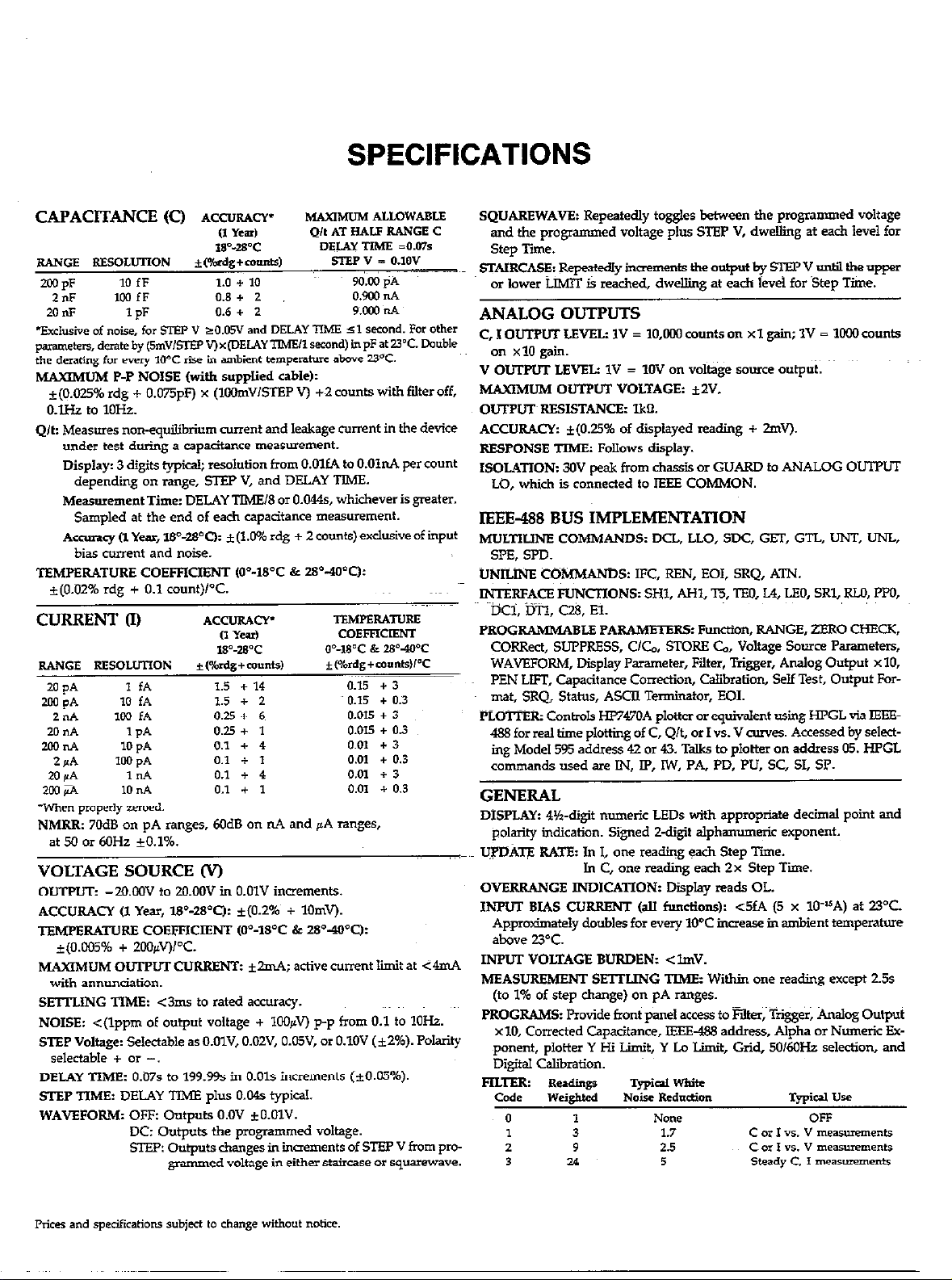
SPECIFICATIONS
CAPACITANCE (C) ACCURACY*
0 Yen,
IBws’c
RANGE REScmmON
mPF
2°F
20°F
+Exdusive of noise, for STEP v am5v and DELAY TIME 51 remnd. For other
parm~w, derateby(~m”,-V)x(DELAY1IMUlrecand) inpFat7.K. Double
the derating for every 10°C rise in ambient temperature above 23’C.
MkylMuM P-P NOISE (with supplied cable):
k(O.O25% rdg + 0.075pF) x (ltiV/STEP V) +2 counts With filter off,
o.lHz to 1oHz.
Q,t: Measures non-equilibrium current and leakage current in the device
under test during a capacitance measurement.
Display: 3 digits typical; resolution from O.MfA to O.OlnA per count
Measurement Time: DELAY TIME/S or 0.044s, whichever is greater.
Accuracy E1 Year, W-WC% * (1.0% rdg + 2 counts) exclusive of input
TEMPERATURE COEFPICIBNT lO”lB”C & 2S”-400Ch
+(O.OZ% rdg + 0.1 count)l°C.
10 fF 1.0 + 10
1w fF 0.8 + 2
1 PF
depending on range, STEP V, and DELAY TIME
Sampled at the end of each capacitance measurement.
bias current and noise.
CURRENT Q
+t?ag+munrr)
0.6 + 2
ACcuRAcK*
” Year)
W-WC
RANGE IlESOLuTfON *wdg+cou*)
20
PA
ZWPA 10 fA 1.5 + 2 0.15 + 0.3
2”A ml fA 0.25 + 6 0.015 + 3
20
Il.4
ml”*
2PA *w
20
PA
*wja 10 “A 0.1 + I 0.01 + 0.3
NMRR: 70dB on pA ranges, 6OdB on nA and pA ranges,
at 50 or 6OHz +O.l%.
1 fA 1.5 + 14 0.15 + 3
IPA 0.25 + 1 0.015 + 03
10oQ
PA
1 “A 0.1 + 4 0.01 + 3
0.1 + 4 0.01 + 3
0.1 + 1 0.01 + 0.3
MAylMuM ALI.cwABLE
Q/t AT HALF RANGE c
DEf.m! TIME =o.m
STEP ” 5 0.10”
5lxQpA
0.900 “A
9~..wo “A
TEMPERATURE
COEFFICIENT
o=wc k 28’MV
*mdg+m”“ts)PC
VOLTAGE SOURCE 0
OUTPET: -2O.OOV to ZO.OOV in O.OlV increments.
ACCURACY (1 Year, lB%WO: i(O.296 + 1OmV.
TEMPERATURE COEPFICIENT to=--WC & 28~4oTb
*(O.COj% + ZOOpVVT.
MAXIMUM OITI-IWT CURRENI: &ZmA; active current Iiit at <4mA
with annunciation.
SE’ITLING TIME: c3ms to rated accuracy.
NOISE: <(lppm of output voltage + lO@V) p-p from 0.1 to 1OHz.
STEP Voltage: Selectable as O.OlV, O.OZV, O.O5V, or O.lOV (iZ%). Polarity
selectable + or -_
DELAY TIME: 0.07s to 199.59s in 0.01s increments (*O.ffi%).
SITP TIME: DELAY TIME plus 0.04s typical.
WAVEFORM: OFF: Outputs O.OV kO.OlV.
DC: Outputs the programmed voltage.
STER Outputs changes in inaements of STEP V from pr*
grammed voltage in either staircase or squarewave.
SQUAREWAVE: Repeatedly toggles between the programmed voltage
and the programmed voltage plus STEP V, dwelling at each level for
step Time.
STAIRCASE: Repeatedly inuements the output by SlEP V until the upper
or lower LIMIT ii reached, dwelling at each iwei for ‘Step Time.
ANALOG OUTPUTS
c, I OUTPUT LEVEL: 1v = 10,wo counts on x 1 gain; 1v = 1Oco counts
on x10 gain.
” OUTPUT LEVEL: 1V = 1OV on voltage sowce output.
MAXMUM OUTPUT VOLTAGE: f7.V.
OUTPUT RESISTANCE: lkn.
ACCURACI: r(O.25% of displayed reading + 2mV).
RESPONSE TIME: Follows display.
ISOLATION: 30V peak from chassfs cm GUARD to ANALOG OurpuT
LO, which is connected to IEEE COMMON.
IEEE-488 BUS IMPLEMENTATION
MULTILINE COMMANDS: DCL, LLO, SDC, GFI; GTL, UNT, UNL,
SPE, sm.
UNILINE COMMANDS: IFC, REN, EOI, SRQ, ATN.
INTERFACE FUNCTIONS: SHI, AHl, T5, ‘CEO, I.4, LEO, SRl, RJR, PPU,
Xi, ‘ml, c28, El.
PROGRAMMABLE PA RAMETERS: Function, RANGE, ZERO CHECK,
CORRect, SLi’PPRESS, C/Co, STORE Co, Voltage Source Parameters,
WAVEFORM, Display Parameter, Filter, Trigger, Analog Output x 10,
PEN LIFT, Capacitance Correction, Calibration, Self Test, Output For-
mat, SRQ. Status, ASCII Terminator, EOI.
PLOTTER: Controls HF747OA plotter or equivalent using HPGL via IEEE-
488 for real time plotting of C, Q/t, OT I vs. V curves. Accessed by select-
ing Mode, 595 address 42 or 43. Talks to plotter on address 05. HPGL
commands used are IN, Ip, IW, PA, PD. PU, SC, SI, SP.
GENERAL
DISPLAY: 4%-d@ numeric LEDs with appropriate decimal point and
aolaritv indication. Sikned Zdkit al~hanuneric exponent.
IJiD‘iTp RATE: In I, one reading wh step Tiie.
OVERRANGE INDICATION: Display reads OL.
INPUT BIAS CURRENT @I functions): c5fA (5 x 10.‘IA) at 23°C.
/,~pmi$~Iy doubles for every 1O’C increase in ambient temperahue
1NP”T VOLTAGE BURDEN: <lmV.
MEASUREMENT SETiUN
(to 1% of step change) on pA ranges.
PROGRAMS: Rovide front panel access to mter; Trim+; tiog Output
x10, Corrected Capacitance, BXEa88 address, Alpha or Numeric Exponent, plotter Y Hi Li+t, Y Lo Limit, Grid, 50/6OHz selection, and
Digital Calibration.
FILTER: ReAngP Typid White
Code we&ted Noise Rechei.m Typid “se
0
0 1 NO”e OFF
1 3 1.7 c or I YS. ” meas-ents
2 9 2.5 c or I YS. ” meanueme”ts
3 24 5 Steady c, I measluemenh
- -.
In c, one reading each 2x step Time.
G TIMEz Within one reading except 2.5s
Page 7

MAXIMUM INPUTz 3oV peak, dc to @IF& sine wave.
nl- COMMON MODE VOLTAGE: 3OV nwimum, dc to 6OHz
sine wave.
NPLT CONNECTOR Isolated BNC on rear panel.
3UTFWT CONNECTORS: Mated BNCs on rear panel for VOLTAGE
SOURCE OUTPUT, EXTERNAL TRIGGER, and METER COMPLETE.
5way binding posts on rear panel for ANALOG OUTPUTs, PEN LIFT,
GUARD, and Chassis.
~rmRHAL TRIGGER: 777, comptiile EXTERNAL TRIGGER and
METER COMPLETE.
-nNIRONMENTz Operating: 0’ to 40°C, relative humidity 70% non-
condensing up to 35OC. Storage: -25O to +WC
XRMUP: 2 hours to rated accuracy (see manual for recommended
pmcedure).
;~~
POWER: 105125V or 21~25OV (internal switch selected), 5OI-k to M)&,
15VA max. 9&llOV and 18X22OV version available upon request.
DIMENSIONS, WEIGHT: l27mm high x 216mm wide x 359mm deep
(5 in. x 8% in. x 14% in.). Net weight 3.2kg (6 Ibs., 14 oz.).
ACCESSORY SUPPLIED: Two Model 4801 Low Noise BNC Input Cables.
ACCESSORIES AVAILABLE:
Model iO19A: Universal Fixed Rack Mounting Kit
Model 10195: Univenal Slide Rack Mounting Kit
Model 4801: Low Noise Input Cable, 1.2m (4 ft.), BNC to BNC
Model 4803: Low Noise Cable Kit
Model 5955: Calibration Standards
Mcdel61134: Test Shield
Model 7007-k Shielded IEEE-488 Digital Cable, lm (3.3 ft.)
Model 7037-Z Shielded IEEE-488 Diittal Cable, 2m (6.6 ft.)
Page 8
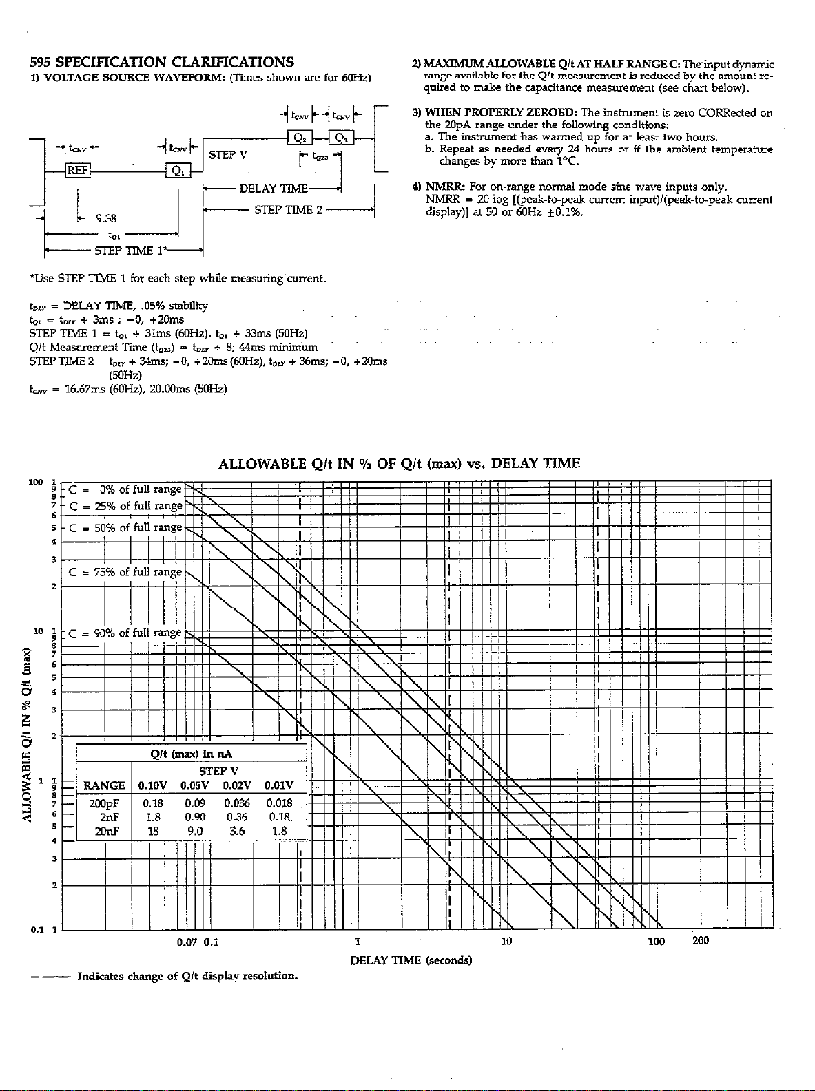
595 SPECIFICATION CLARIFICATIONS
U VOLTAGE SOURCE WAVEFORM: (Tiies shown are for 6OHz)
< c 9.38 I j---s~p------
*Use STEP TIME 1 for each step while measuring current.
t,, = DELAY TIME, .05% stability
b, = t,, + 3ms ; -0, +ZOms
STEP TIME 1 = bx + 31ms (6OHz). ton. + 331x (5OHz)
Q/t Measurement Time (to.,) = torr + 8; 44ms minimum
STEP TIME 2 = t,, + 34nxs; -0, +ZOms @Hz), t,, + 36ms; -0, +20ms
(5OHz)
t, = 16.67ms (6OIiz). ZO.Wms (5OHz)
2) MAXIMUM ALLOWABLE Q/t ATHALFRANGEC: The~input dynamic
range available for the Q/t measurement is reduced by the amount required to make the capacitance measurement (see chart below).
3) WHEN PROPERLY ZEROED: The instrument is zero CORRected on
the 2OpA range under the following conditions:
a. The instrument has warmed up for at least two hours.
b. Repeat as needed every 24 hours or if the ambient temperature
changes by more than 1°C.
41 NMRR: For on-range normal mode sine wave inputs only.
NMRR = 20 log [(peak-to-peak current input)@?&-to-peak current
display)] at 50 or 6OH.z +O.l%.
ALLOWABLE Q/t IN % OF Q/t (maw) vs. DELAY TIME
0.0, 0.1
--- Indicates change of Q/t display resolution.
1
DELAY TIME (seconds)
10
100
200
Page 9
TABLE OF CONTENTS
SECTION l-GENERAL INFORMATION
1.1 J.N”IRODUCTION
1.2
1.3
1.4
FEATURES
MANUAL ADDENDA
SAFETYTERMS
.................................................
.......................................................................
.....................
........................................................ ..,__
UNPACKING AND INSPECTION
E
1.7
1.8
REPACKING FOR SHPMENT
WARRANlY INFORMATION
ACCESSORIES
.................................................................
.... ______
.....................................................
SECTION 2-GETTING STARTED
2.1
2.2
2.2.1
2.2.2~~
2.2.3
2.3
23.1
2.3.2
2.4
2.51
2.5.2
2.5.3
2.5.4
2.55
2.56
2.5.7
INTRODUCTION..
PREPARHION FOR USE
LinePower.. ..................................
LineVoltage Selection ........................................................................
LieFrequency
POWERUPPROCEDURE
PowerCord.........................~....................~....--.........................~
Defaults..
.............
RAM and ROM Test Messages
GENERAL DISPLAY MESSAGES ................................
INSTRUMENT FAMILIARIZATION.
Model595FrontPanel...............................---......-......-..-..........-....~~~~
Model595RearPanel..
Test Cormxtions for Capacitance and Ctient Measurements
Capacitance Example
CVExample.. ..................................
Measurin‘g Current: AnExample
IV Example ............... ._. ._..__ ._
...................
.......................................................................
.................................
..............
_______
..............
..........................................................................
_.__ __
_
..........................................
..
...............................................................
...............................................
..........
_
.............................................
..~. __r______
.................
.._
_
...............................
.
.....
.
....................................
............................
.......
..__
_._~_
.........................................
........
................................................
_.
. . _____ _..._....._........_~
___._ . .,._
.............................................
................................
................
._____
.._
_._
.............. l-l
......................
__ __ .....
.............
._
...........
.._
_._l .,_.____.
_._~_.______._.
.................................
........
_,
~:
.............................
..............
__
............................. 2-6
....................................
.._ .............................. 2-9
......
.................
. . .
.
. . .
................
.......
...
___
_.
...
.,
..
..~2- 1
...
....
;...~2- 2
_~__. 2-2
..
l-l
l-l
l-1
l-l
l-2 ..
l-2
l-2
2-l
2-l
~2-1~
2-l
2-l
2-l
2-2
2-2
2-4
2-7
2-8
2-n
2-12
SECTION 3-OPERATION
3.1 ;i INTRODUCTION ___._......~..___._........................... ___ . . . .
PART i-Front and Rear Panel Description
3.2
3.2.1
3.2.2
3.3
3.3.1 ..
3.3.2
TEST CONNECI-IONS
Cap&zitance C$yeclions
Connections for Cment Measurements
DETAILED FRONT PANEL CONTROL DESCRlPnONS
CURRENT
CAPACITANCE.. .....................
33.3 ~cl~-mREc,.
y. : SUPPRESS
ZERO CHECKand CORRect.......~..........~.........................I
RANGE A, v.. .........................................
A LIM.IT, v LIMIT and PRESET
3.3.9
DELAY TIME
.....
_,_ __._. I_____~~. . _.
................................
....................................................
............................................................
........................................................................
....................................................
.......................
.......
...............
_
; ;
...............
__.,__ _ .. . . . .._-... 3-l
.........................................
...........................................
..~ ...
____ ___.__. .............................................
_..__
................
......................................................
__ _.
. .
.
. .
.
. . . . . . . . . 3-l
. .
. .
. .
. .
. .
_.-
~. . . . . .
.............
__ _
~;.;.
...................... 3-2
..-
......
.__.
_._
.......
.......................
.._
.............
__ . _
.......
......
3-l
3-2
3-2
3-2~
3-3
3-3
3-3
3-4
3-5
3-5
Page 10
3.3.10
3.3.3.11
3.3.12,
3.4
3.4.1
3.4.2
3.4.3
3.4.4
3.4.5
3.4.6
3.4.7
3.4.8
3.4.9
3.4.4.10
3.5
3.5.1
35.2
3.5.3
DISPLAY SOURCE
ADJUST A , V
+I-, Front Panel Trigger .......................... ._
FRONT PANEL PROGRAMS ................... :_ .. __ ._ ........................................... 3-6
Power Lime Frequency.. ............... ..___
Calibration
Filter. ................................. ..~~-.........................~ ........................
Trigger .............................. ~...;.~..;.;~. ....................... . ............. :.~..:.~ .. 3-10
Andog output xlmo
C~irectedCapacitance ........................................................................
IEEE-488Address..~..................................................................~..~ .... 3-11
Display (Alpha or Numeric) .................................................................. 3-11
Grid ....................................................................................... 3-13
Y HI-YLO ................................................................................ 3-13
REAR PANELS
ExternalTrigger.. ...........................................................................
MeterComplete....................................................................~--.- .... 3-14
Analog Output .............................................................................. 3-M
..........................
FEATURES.. ......................................................................... 3-13
..........................................................
.................................................................................
...........................................
.._.._._
...
..~.~---------................~.~............~~~ ........ 3-8
........................................................................
...................
.._.
.:~.~..;..I~;
...................
.......
3-6
3-6
3-6
3-8
3-8
3-71
%J.I
3-13
PART 2-MAKING CV, IV or Q/t-V Plots
3.6 SETTE’JG UP THE TEST FIXTURE .............................................................
3.7 SETTING UP MEASUREMENT PARAMETERS .................................................. ::
3.8 BEGINNINGTHEMEASUREMENT..
3.9
3.10 ANALOG PLOTTING ..........................................................................
3.11 PRINTING RESULTS .......................................................................... 3-19
3.12 USE OF JXI’ER ON CURVES ........................................... : ...................... 3-20
3.13 MEASUREMENTCONSID~ONS..;..~ ... .._. .......... .._._ ...................... . ......... 3-22
3.X3.1 Ground Loops .............................................................................. 3-22
3.X3.2 Electrostatic Interferences ....................................................................... 3-22
3.13.3 The~~EMFs.............................~...;...........~
3.X3.4
3.13.5
3.X3.6
D.&TALPLOTTING
RFI ........................................................................................ 3-23
Source Capacitance ......................................................................... 3-23
Engineering Units Conversion .................. 1.. ....................... ;. ..... ;~. ;. ............. 3-24
...................................................................
...................... . ....................................
..................................
~;
.......
3%
3%
3-19
3-23
SECTION 4-IEEE-488 PROGRAMMING
4.1
4.2
4.3
4.3.1
4.3.2
4.4
4.5
4.6
4.6.1
4.6.2
4.7
4.7.1
4.7.2
4.7.3
4.7.4
4.8
4.8.1
4.8.2
ii
INTRODUCTION .............................................................................. &l
SHORTCUT TO IEEE-488 OPERATION .......................................................... 41
BUS CONNECTIONS ....................... _.,_-,_ ...................................... .~_ ........ 41
Typical Controlled Systems ................................... .; ................................ 41
Cable Connections .. .._ ...................................................................... 42
PRIMARY ADDRESS PROG RAMMING ......................................................... 4-4
INTERRACEFUNCTIONCODES..;.;..;;. ............. .
CONI’ROLLER PROGRAMMIN
Controller Handler Software ..................... :. ............................................ 45
Interface BASIC Pro gramming Statements ........................................................ 4-6
FRONT PANEL ASPECTS OF IEEE-488 OPERATION ............................................. 4-6
BusError........................................................................~ ............ 46
TriggerOvemmE~or ........................................................................ 47
Number and Conflict Errors
WaitingforTriger ........................................................................... 47
GENERAL BUS COMMAND S
REN (Remote Enable) ........................................................................ 48
IFC (Interface clear) .......................................................................... 48
G ................................................................. 45
...................................................................
......................................................................
.............................
..;.
........
4-4
&7
48
Page 11
4.83 LLO (Local Lockout) .........................................................................
4.8.4
4.8.5
4.86 SDC(SelectiveDevice clear) ................................................................. 4-10
4.8.7 GET (Group Execute Trigger) ................................................................. 410
ES ~;
4.9.1
4.9.2
4.9.3
4.9.4
4.9.5
4.9.6
;:;; ~:
4.9.9
4.9.10
4.9.n
4.9.12
4.9.13
4.9.14
49.15
49.16
4.9.37
4.9.18
4.9.19
4.9.20
4.9.21
4.9.22
4.9.23
4.9.24
4.9.25
4.10 PROGRAMMIN GEXAMYLES
4.10.1 Square Wave Capacitance Measurements ....................................................... 4-48
4.10.2 StaircaseMeasurements
4.10.3 Cti@ntMeasurements ........................... .
4.11
4.12 IEEE-PLOT..
4.13
GTL (Go To Local) and Local ..................................................................
DCL(D&ce Clear) ..........................................................................
SPE, SPD (Serial Polling). ..................................................................... 4-10
DEVICE-DEPENDENT CO
Programming Overviav........~ .............................................................. 4ll
Execute (X) ................................................................................. 4-16
Display (D) ................................................................................. 417
FundionO.................................; ............................................... 4-18
Ran@(R). .................................................................................... 419
ZeroCheck,ZeroCorrect(Z). ...... . ............ ;.~. ..... I..................... Y . ..i.. ....... 420
Suppress (N) ................................................................................ 421
F&r(r). ....................... ;..~.~.l~.~....~ .:. .... . ................ . ......................... 422
Egh Limit (H) ............................................................................. 423
Low Limit (L). ................................................................................ 424
Voltage Source (V) ........................................................................... 425
Step Voltage (S) ............................................................................. 4-26
Delay Tie (I) .............................................................................. 427
wavefoml (W) .............................................................................. 428
c/c,J (C) ................................................................................... 429
CapacitanceModifiers ................................................ . ............... :1~.~~430
Pr&s (G)
Analog output (0). .........................................................................
TriggerModeo.............~.....~............................................; ............
SRQ Mask (M) and Serial Poll Byte Format.
EOI and Bus Hold-off Modes (K) ............................................................. 438
Terminator(y).
status (u) .................................................................................. 44
Digital Calibration (A) ....................................................................... 446
Self-Test and Permanent Memory Storage u) .................................................... 4-47
TALK ONLY
BUS DP;TZ1TRANSMISSIONTIMES ............................................................ 450
........................
.............................................................................
..................................................................................
....................................................................................
IvcGANDs :..: ......................................................... 4u
.......................................
.~I~.
....................................................
....................................................
......................................................................
...........................................
..............
;
...........
:.~:.
49
49
49
; 431
433
434
435
4-40
~4-48
4-48
4-49
4-49
4-49
SECTION 5-APPLICATIONS
5.1
5.2
5.2.1
5.2.2 Voltage Coefficients of High Resistances
5.2.3 IVCharacteristicsofDiodes
5.2.4
5.25
5.3 APPLICATIONS OF THE CAPACITANCE FUNCTION
5.3.1
5.3.2 Characterizing the MOS Capacitor in Depletion and Accumulation
5.3.3 Characterizing the MOS Capacitor in Inversion
5.3.4
5.3.5 ~:
5.3.6 Comparison of the Feedback Charge Method with the Traditional Ramp Method
5.3.7
5.4
INTRODUCTION
APPLICATIONS OF THE
HighResistanceMeasurements...................................~ .............................
IV Characteristics of Transistors
~w LevelLeakageCurrentMeasurements ..................................................... 5-6
Ccmsiderationsfor CapadtanceMeasurem~nfS;.~.;;~.~;. ........... 1.~.
Determining Delay Tiie for Equilibrium Measurement
MOS Non-equilibrium and Roper Use of the Corrected Capacitance Program .................... 5-13
Comparison of the Feedback Charge Method with the Static or Q-V Method ...................... 5-19
BIBLIOGRAPHY OF QUASISTATIC CV MEASUREMENTS AND RELATED TOPICS
..............................................................................
CURRENTFUNCTION ...... __._._
..........................................................
...................................................................
...............................................................
...............................................
..................................................
..........................................
................
...............................
. .................... 5-l
............
5-l
5-1
5-l
5-2
5-4
5-S
.:.............. 54
5-8
5-9
510
.................. 5-17
................
5-21
iii
Page 12
SECTION C-PERFORMANCE VERIFICATION
6.1 INTRODUCTION..
6.2 ENVIRONMENTAL CONDITIONS
6.3 INITIALCONDITIONS..
6.4
El
6.5.2
65.3
6.5.4 Capacitance Verification
6.5.5
RECOMMENDEDTESTEQUIPMENT.. ............... .,.:.
VERIFICATION PROCEDURES
InputCurrentVerification....................:.........................................~
Current Verification
Q/t Verification
Voltage Source Verification
............................................................................
..............................................................
......................
......................
......................
...............................................................................
.................................................
....................
SECTION 7-THEORY OF OPERATION
7.1
7.2
z3
%4
%4.1
%4.2
%4.3
7.4.4
7.5
z5.1
Z5.2
z5.3
z5.4
76
7.7
Z8
z9
ZlO
7.10.1
7.102
z10.3
ZlO.4
z10.5
ZlO.6
7.11
7.12
INTRODUCTION
CVMEASUREMENTMETHOD.. ...............................................................
OVERALL FUNCTIONAL DESCRIPTION
VCKTAGESOURCE.. ........... .................
D/A Converter
PrecisionStep Source.................................................~...............~
Output Stage.. ...........................
ResetCircuit.. .........................
PREAMPHFIER..
PreamplifierConfiguration..
InputandGain Stages................................................~
FeedbackElements..
Past Discharge Bridge .................. . ..................
Xl0 AMPLIFIER
MUITIPLFXER and BUFFERAMFLIFIER
-2VREF!.XF!NCESOURCE _ ..........
A/D CONVERTER..
DIGITAL CIRCUITRY
Microcomputer...........................~...-......................................-
Memory Elements
Device Selection.......................................................................~
IEEE488Bus..........................~..~..~.~
Input/output circuitry..
-. . -. .~
I&play cacti
ANALOG OUTPUTS
MAIN POWER SUPPLY
.............................
.......................................................
......................... _~.._
............
.....................
........................
..................
...........................................................................
...................................
..................... ,^.,..., -
............................................................................
...................
.......................................................................
____; ...........................................
.......................................
:.
............................................
.~___.
.....................................
.,_
..........
;. .......
_.
...............................................
..............................
i..;.;
.1..~
~.~.~._~._~_~.~._~.
.~;.Z;; __
........................................................
:.:::.:.‘; .... ~-..:;...;.~...:‘...:.:.:..:_..:.;..;.~;....::;..I~;’
.: .:.~.:~I~.
_.
.................
._ ..__
..-_ ._
...................
.... .1.~. .... .;....... -y..;...;;
....................................................
............................
..........................
...................
.................................................
..
.
.I
...........
..............
..~................-.--.........~
......... ..__
_.
......................................
... . . . . . . . . . . . . . . . . . . _.
;.
.:
.~;~I..
.....................
_._._ ..: .............. .._ .........
.................................
_
...............
.., .. ._ ........ ______,_________
__
........................
.
_,.___ _.___.__~.
.....
;.;.
... .1..~....‘.....1.....
......................
........................
.._
.__-____
_,
.........
.,,
.........
., _._,
.........
..............
..........
1-..~
..:
........
............
........
......
.........
.......
.....
....
64
E
6-1
6-2
6-2
6-3
6-6
66
6-7
7-1
7-1
7-2
7-Z
7-2
7-5
7-5
7-a
7-8
7-8
7-10
Ku
7-12
7-14
7-14
7-26
7-16
7-18
%I8
7-18
%I8
7-19
7-19
7-20
7-20
7-22
SECTION 8-MAINTENANCE
8.1
8.2
8.3
8.4
8.5
85.1
8.5.2
8.53
8.5.4
8.5.5
8.5.6
iv
INTRODUCTION
LINE FREQUENCY SELECTION
LINE VOITAGE SELECTION
FUSE REPLACEMENT
CALIBRATION
Recommended Calibrated Equipment
Environmental Conditions
Warm-Up Period
Ca&ration Jumper
;Frt$yr
.....................................................
.......................
.......................
.........................................................
......................
ration..
.....................................
......................................................................
~..I~.:.~:.
._
..........................................................
...................
...........................................
.....................................................
__.
.....
.~.~_._-~__
...............................................
.,
................................................
............................................
....................
_,
.........................
__
........
.;
.......................
_
_
.....
.....
_ .................
_.
..................
_.
..............
...................
8-l
8-l
81
8-2
8-2
8-2
8-3
8-3
8-3
8-5
8-5
Page 13
._~.
8.5.7 Calibration Sequence ............. ..
8.58
8.5.9 Input Offset Voltage Adjustment
8.5.10
8.5X Input Current Adjustment
8.5.12 Capacitance Offset Compensation
8.5.73
8.5.14 Current Calibration
8.5.15
8.5.16
8.5.17
8.5.18
8.5.19 Additional Calibration Points
8.6
8.7
8.8 TROUBLESHOOTING ........................
8.8.1
8.8.2
8.8.3
8.8.4
8.85-- AIDConverterChecks.. ...............
8.8.6
8.8.7 Relay Configuration........~
8.8.8
8.8.9 Digital Ciitry
8.8.10
8.9
8.10 HANDLING AND CLEANING PRECAU'IIONS
DigitalCalibration....................................................~
............................................................... 8-6
Zen,HopCompensation......................................-....-
.................................................................... 8-8
Voltage SourceCalibration..
............................................................................
1,CAnalogOutputAdjustment ...............................................................
Q/t CaIibration
Capititance Calibration ......................................................................
Storage of Calibration Parameters
... DISASSEMBLY INSTRUCTION
SPECIAL HANDLING OF SIXTIC SENSITIVE DEVICES.
RecommendedTest Equipment ................................................................
Power UpSeIfTest
Self DiagnosticProgram ......................................................................
Power Supply Checks. .......... .._
Voltage Source Checks
Input Conditioning Circuitry Checks
DisplayBoard Checks
INPUT STAGE BALANCING PROCEDURE .......................................................
........................................................
.......................................................................... 8-18
.............................................................................
..................................................
......................... _,
................................................................. 815
.................................................................. M5
................. ~....; .... .
................................................................. 8-24
..............
........
.............................................................
.....
.._
..........................................................
.._..............~....~..................~............~ ... 8-30
__
_
..... _ ....................................
..
........................ 8-6
.......................... 8-7
..-
.............
__ _.
....................
...................................
.....
__.__.; ....... .._. ................................ &l7
.......................................
:;.~
...................................................
.....
_.__.:
..................................................
...
._
_.
............................
....................................
___.._.._
...
8-6
8-8
8-8
a10
813
&I3
&I.3
8-14
8-17
&I8
818
8-19
8-19
~8-19
8-24
8-24
8-31
8-31
SECTION 9--REPLACEABLE PAFiTS
9.1 ~~. INTRODUCTION. . . . . . . . . . . . . .___. . __. _. _. _. _. . . .__. . . . . . .__. _. . . . . . . . . 9-l
9.2 PARTS LIST . .._...._.... . . . . . ._ .___..__.._._.._._. .,. ..~ ._._._____.___.. . .._. .__.. . . . . . 9-l
9.3 ORDERING INFORMATION . . . . . . . . . . _ _ . . . . . . . _ _ . . . . _ . . . . . . . . . . . . . . . . . 9-1
9.4 ~~ FACTORY SERVICE . __. ..____ .__~__~.~ ____ .___~ ____ _____ ______. __. . __. .___. . . . . . . . . . . . . . . . . . 9-l
9.5 S-C DIAGRAMS AND COMPONENT LOCATION DRAWINGS . . _ . . . . _ _ _ . _ . . . _ . _ _ _ _ . _ _~. . 9-l
APPENDIX A
APPENDIX B
APPENDIX C
APPENDIX D ......................................................................................
APPENDIX E .......................................................................................
APPENDIX F .......................................................................................
APPENDIX G ........................................................................................
APPENDIX H
.......................................................................................
..........................................................................................
A-l
B-l
...................................................................................... C-l
D-l
E-l
Gl
...................................................................................... H-l
F-l
v/vi
Page 14
SECTION 2-GETTING STARTED
LIST OF TABLES
2-I.
Display Messages . . . . . . . . . . . . . . . . . . . . ;~.- .._.. _ ___............_............. . . . .._ . . ..~.....~.~Y ..,.,.. 2-3
SECTION 3-OPERATION
FrontPanelPrograms.................................................~.......................-
z
3-3
Display ExponentValues .......................................................................
Engineering Units Conversion
...........................
SECTION 4-IEEE-488 PROGRAMMING
41
42
43
4-4
45
t73
IEEE488 Contact Designation ...........................................................
Model 595 Interface Function Codes.
BASIC Statements Necessary to Send Bus Commands ...............................................
IEEE-488FrontPanelMessages ...............................................................
General Bus Commands and Associated BASIC Statements
Device-Dependent Command Summary .........................................................
Bus Hold-Off Ties ................ __ __
Trigger to Reading Ready ‘Iiies~ (in Ksec) ..........................................
............................................................
....... _
SECTION B-PERFORMANCE VERIFICATION
Recommended Test Equipment for Performance Verification.
2
6-3
6-I
6-5 ...
Liits for Current Verification
DeterKnin g Capacitance Limits ....................................................................
CapacitanceVerification .........................................................................
Limits for Voltage Source Verification ................................................................
...........................................
1.
...................................
.........................
................................................
........................................
_ ..........
.. 3-7
3-12
:.
3-24
..
_ ........ 44
45
46
..- 46
., .............. 48
4-13
438
.-I
..........
: ............. 6-3
., . 450
6-2
6-6
6-7
6-7
SECTION 7THEORY OF OPERATION
7-1
7-2
RelaySwitchConfiguration..
Memory Mapping ..............................................................................
................................... ~..~.;.:..Y.~ .._.
SECTION S-MAINTENANCE
8-1
8-2
8-3 ..
8-4
8-6
Lie Voltage Selection (50~&X-Iz) ................................................................
Line Fuse Selection .............................................................................
Recommended Calibration Equipment
Current Calibration ..............................................................................
Capacitancecalibration ........................................................................
Recommended Troubleshooting Equipment
DiagnosticProgramPhases.........~ ............................................................
...........................................................
......................................................
...... .I
...........
~..~?ll
7-1
_ 8-l
8-2
8-3
8-u)
8-X
8-18
8-19
vii
Page 15
8-8 PowerSupplyChecks
A/D~~Converter Checks
Voltage Source C,hecks
Relay Confiitihon
Amplifier Cams
833
a14
845
846
al7
Capacitance Circuitry Checks
Cu&ntCktiitryChecb
Digital Circuitry Checks
DisplayCircuitryChecks..
InputStageBalancing................-......~...........--...........-.-........~----...-~~~
...............................
..............................
........................................................................
....................
.............
...........................
........... ..__. _ .~-.
.._...........~~.~.~.........~.~..............~~.~...............~
........................................................
.............
SECTION g--REPLACEABLE PARTS
.-__-___
.
................
.....................
.
.........................................
~___~ .
...................................................
__~.~~.-~_~~__.
........................
..___.__. _..__
- .. -
...........................
_.,..-. _,_._.
..............
................ -
...
.,
.
...............
.~.~...~.~__ . 8-28
......
.......
....
_,_
8-19
8-20
i$
8-25
8-25
8-27
%3:
...
9-1
9-2
9-3
9-4
MotherBoard,Parts List....................................~~.~~..~
Display Board, Parts List..
Preamp Board, Parts List
Miscellaneous Parts, Parts List
.............................................
........................
............................................................
APPENDIX D
D-l
BASIC Staten-tents Necessary to Send Bus Commands . . . . . . _ . . . _ _ . . . . . . _ :. . _ . . D-l
APPENDIX F
Fl
F2
~-3 Typical Addressed Command Sequence.. . . . . . . .
M
F-5
IEEE488 Bus Command Summary . . . . . . . . . . .,~ .,__ ~___.~ __....__.._... .____.. ._. _. __ _..~ ..____ “TV... W
Hexadecimal and Decimal Command Codes.. . . _ _ . . _ _ . _ _ . . . _ . . . _ _ . _~_. . . . . . _ . . . . . _ . . F7
Typical Device-Dependent Command Sequence. . . _ . _ . . . _ . . . . . _ _ _ _ _ . _ _ _ _ _ __ _ _ _ _ _ _ . _ _
IEEE Command Group . . . . _ _ . _. . . . . _ . _ _ . . ___. _~_ ._ . . . _ . . . . _ . . . . . . . . . . _. . _. . . . . F7
APPENDIXG
Device-Dependent Command Summary . . . _ . . _ . . . _ _ _ . _ _ _ _ _ . . . . _ _ _ _ ..- _ _ _ _ _ __ _ _~_ _ _ . .
.............................
..~.
.............
............
..
.‘. I
:
. . . . ~.~ _,.. _.~ _.__ * . . . . _ . . . . . . . . . . . . . . . . . . . . . . . . . .
:
......
......................
_
.........
.
._
....
9-2
9-15
9-21
9-27
F7
M
G-l
Page 16
SECTION 2-GETTING STARTED
LIST OF FIGURES
2-l
2-2
2-3 Typical Capacitance Measurement Corinetions . . . . .~. . . _ . _ . . _. . . . . . . . _ . . . . . . . . . . . . . . . . . . . . . . 2-7
2-4 Typical Cment Measurement Confections . . . . . . . . . . . . _ __ . . . _. ., -- ., . . ., . - -. . .,., . . . . . . . . . . . .~.
Model 595 Front Panel
Model 595 Rear Panel .
.._. . . . . . . . . . . . . .._..___... . . . . . . . . . . . . . . . . . .._.... . . . ~.-~ .._... _.__ ,...
. . . . . . . . . . . . . . . . . . . . . . . . . . . . . . . . . . . ..-...................................
z-j
2-7
SECTION 3-OPERATION
..-
_~_
...
..
..
3-l
3-2
3-3
3-5
3-9
3-10
3-14
3-14
3-18
3-22
CapacitanceMeasurementConnections.
ii
3-3
3-4
3-5
34
3-7 &&md Trigger P&e Specifications ............. .., .................................................
3-8
3-9 NCurvesofa6.3VZenerDiode..
tt
3-z
Cbnnections for Current Measurements.
Integrator Charge vs Tme Cur+ Ior a Capacitance Measurement
VoltageOutput Waveform
Exainple:UsingtheFilteronaMOSDevi@Cu.rve. ................................
Coefficients in Filter 2
Meter Complete Pulse Specifications
MOSDeviceCVCurvewithFilters. ........................
~MultipleGroundPointsCreatingaGroundLoop..
EliminatingGrotidLoops.
..................
.........................
........
...........
.................
.
.........................................................
...............................
.
.......
. __
.
......................................
._, __ __
........................................
..-......................-.~..~...~~.-.~
.......................
~...~_.._.~.._
..
..
_,__.
..................................
.._._..,
........................
.............
.
... ............
.........
..~
__ _,_
.._ _____
........
.~~.------
..........
.....
.._._..._. 3-21
.....
..............
.......
.._
..............
_.._
.
........
__.._ _ _,._._ ., .._ ~.~3-22
;.m.
SECTION 4-IEEE-488 PROGRAMMING
....
42
43
43
44
432
437
442
443
4-44
.
.
2
41
42
43 IEE.E-488~connections..
44 Model 595 Rear Panel IEEE-488 Connedor
45
4-6
47
z
4la
4l.l
zg
SystemTypes
~IFXE-488 Connector.............................................................---.~....~.~..~~4 2
ContactAssignments...........................................--.-.....-........~- .............
GeneralDataFormat............................----.......................- ..................
SRQ Mask and Serial Poll ByteFormat.......................- ..................................
UO Machine Status Word (Default Conditions Shown).
~UlErrorStatusWord
U2 Data Status Word
U3DelayTme
U4VoltageSourceLfrmts
U5 Voltage SourceBlas Se~gs
.................
..................................
............................
.......................................................................... 443
.... . ...............
.....................................................
..~..~.-.~-~........~.....-~-.-.-..-.~.............-
..-......-.-- .............
.................................
...........................................
_..,_
.........................
___.~.~
.........................................
_____~_ _,.-_....,
.,
.................................
.............
.........................
.....
.,
__,__
.._....._..,._
.._
.............................................
_~^.
.
........
SECTION 5-APPLICATIONS
5-1
5-2
5-3
5-5
Current Measurement Corrections Using the Model 595 Voltage Source.. . . . . _ _ _ . . . . . . .
NCharacteristicsofaZenerDiode(5.1V)lN751.....___..___._ ___ _.___ ____ . ..__. _ ..___.__.._.... 5-3
Connections for Bipolar Common:Emilter N Characteristics . _ . _. . . . . _ .,_ . _ _ _ _. _ ______ _ _ . . _ . _. 5-4
Typical Bipolar Common-Emitter Characteristics . . . . . . . . . . . . . _ _ . _ . . . . . _ . . _ . . . . . . 5-4
Conmctions for Common-Source FET N Characteristics
5-l
_ _ _ . . . . .~. . . . . . . . _ . _ _ . _ _ _ . . . . _ _ 5-5
ix
Page 17
5-6
5-7
5-8
5-9
5-10
5-11
5-12
Typical Common-Source FET lV Characteristics
Leakage Current Measurement.
................
Ca~acitorLeakageTests .......................................................................
cvs.vGwe..
.........................
Equivalent Circuits of the MOS Capacitor.
..-- .- ~.~..~_
...............................................
Recognizing Equilibrium Using C and Q/t VS. Delay Tie: Inversion: Substrate Voltage = +8V,
Squarewave Test Signal = +O.OZV
............................................
Corrected vs. Uncorrected CV Curves of a SimulatedLeaky Capacitor C(corrected) = C-(Q/t)
(StepTiie)/(VStep). .................. -.~ ..:.
5-13
5-14
5-15
5-16
5-17
Recognizing Equilibrium Using C vs. V and Q/t, ys,~,V
Misuse of Corrected Capacitance Program-on Non-Equilibrium Curves
Comparison of ~Quasistatic CV Methods
FrequencyResponse..
....................
Comparison of Quasistatic~ CV Methods
.......................................................
.......................................................
SECTION 6-PERFORMANCE VERIFICATION
6-l
6-2
6-3
6-4
Test Fixture Construction..
.............................
Setup for Current Verification (2001x.4 to 200SA Ranges)
Setup for Current Verification (2Op.A to 2OnA Ranges)
Setup for Voltage Source Verification
.................................................
SECTION 7-THEORY OF OPERATION
.......................
....................................
._
.................
......
................
.
..................
...........................................
......................
__ .,_.
..
_
._
,_.
..
.._ _
......
YI..;
..__
....
.. 1 .............
YT T
.......
..
:~.
..........
..................
..
_. __
_,_-__.
--.~.
1~;.
.......
-.
......
.....
............................. 5-16
;
..~........~.....-.......~
............................................ 6-l
.:
....
..............
_.
__ __.
......
.......
-._~.lT~-
.......
__ ._
.. _ ...
...
...
....
5-5
5-7
5-8
5-9
5-9
5-12
5-x
5-15
5-18
5-19
5-20
6-4
6-5
6-8
7-l
7-2
7-3
7-4
7-5
7-6
7-7
7-8
7-9
7-10
7-11
7-12
7-13
7-14
7-15
7-16
7-17
7-18
7-19
Feedback Charge Method
TiingVoltageandChargeWaveforms
Model 595 Simplified Diagram
Voltage Source D/A Converter Circuitry
PrecisionStep Source...............................................~.................~ ........
Output Stage Circuitry (Simplified)
Current Limiting for Output Stage
Voltage Source Reset Circuitry
BlockDiagramofInputPr~ampIifier.....................................~
Circuit Configuration for Current and Capacitances
Input Stage and Gain Stage
FeedbackElement ............................................................................
FasfDischargeCircuitry.. ..................
XlO~Amplifier Circuirry.......................................................~...........~.~
Multiplexer and Buffer
Multiplexer Phases.. ..............................................
-2V Reference Source
A/D Converter
Analog Outputs
...................................
..............................................................................
SECTION 8-MAINTENANCE
8-1
8-2
8-3
L-2
8-6
8-7
~Test Fiiture~~Conshuction
Calibration Jumper and Calibration Pots
Equipment for Zero Hop Compensation
Voltage Source Output Calibration Setup
V Analog Output Calibration Setup
Current Calibration Setup (200pA and 20nA Ranges)
Current Calibration Setup (20pA to 200& Ranges)
........................................................................
............ _~.:. .......................
..........................................
.................
:.
...... _ ......... .;
............................................
.................... ._
...............
:
..........
............. _ _,_ ......
...............
:
..................
...........
................................................
.~;
:~
...................................
........................................................................
........................................
.................
..;
...................................................
...................................
...................................
...............
- ..................
........................................
.......................
.............................
...... I
_~I
...........................
..I
.......
__
......................
............ .I
;
..,
................
........
........................
_.
..:.
~.;
........
..........
., . .~l.-. ...........
._
......
................
-.:.::
............
..
:
:.
.
.
. . .
.
.
,..
. . .
. . .
7-l
.....
_
....
7-2
7-3
7-4
:.~.
.,
........
7-5
.......
.._
7-6
7-7~~
........
.,
7-8
7-9
7-9
......
.;.
7-10
7-12
it
......
7-13
..
7-14
.
.,_, 7-15
.__
..
.;. .~I
......
....
7-16,
7-16
7-17
7-21
. ..~:;. ...... 8-2
............ 8-4~
............ 87
............ 8-9~
............. 8-9
........... 8-11
............
~812
x
Page 18
C, I Analog Output Calibration Setup
Model595EqkdedView
8-10 Input Stage Balancing
......... _ __
................ ..___
..........................................................
.............................
.....
.__,.___ _____ _
. .._ . .__.,._...._._
.,__ - .._
.,_ .
..................
_
_
.. . .
.,
..
...... 8-13
......
_,
...
816
8-32
SECTION g--REPLACEABLE PARTS
9-l ~~ Mother Board, Component Location Drawing, Dwg. No. 595-100 _ . _ _. . . _. . . _ _. . . . _ _ _. . _. . . . _. . _ . 9-8
9-2
9-3
9-4
9-5 & Board, Component Location, Dwg. No. 595-160 . . . _ . . _ _ _ _ . _,_ _ __ .,. _ _ . _ _ . . . . . _ . _ . . . . 9-24
9-6
Mother Board, Schematic Diagram, Dwg. No. 59X06 _ . . . . . ___ __ . . _ _ _. . . . . _. _. . . ___ _. __ _ ._ . . . 9-9
Display Board, Component Location, Dwg. No. 595~ll0 _ _. _ _ _ _ _ _. _ _ _. _. . . . _. . . _ . . _ _ _ . .~.___~_ . . __ _ 9-18
Display Board, Schematic Diagram, Dwg. No. 595-116 . . . . . _ _ _ . . . . . . . _ . _ . . . _ . _ . . . . . _ _ _ _ . _~_ _ _ .9-19
Preamp Board, Schematic Diigram, Dwg. No. 595-166. . . . . _ . . .; _ _ . _ . _ __ . . . _ _ _ _ _ _ _ _ _ . _ . . _ . _ . . . 9-25
APPENDIX F
iEBE.BusConfiguration . . . .._..__._.._ _,_ _______._._. ~I __.___._ ______ .._.... _ __...__ _ ___.__.._.._..
IF,EB488HandshakeSequence _......_.__ ~...:~ __..__. _ _._.......___..._ _ .._. _____.__ .__.____._ _.__ F3
~3 Co-andcodes . .._......__....__....~. _.._.. _ .._. _ ._.__......_....--. _ .-.- ~_-_ _--.... _.._ .-..... F6
M
xi/xii
Page 19
SECTION 1
GENERAL INFORMATION
1.1 INTRODUCTION
The Keithley Model 595 Quasistatic CV Meter is a sensitive
instrument designed to measure capacitance and current.
The Model 595 uses a unique feedback charge method to
stimulate and measure charge steps in the device under
test, from which capacitance is determined. (A DC voltage
is ah available to make basic current measurements). This
method of measuring capacitance is superior to the traditional ‘%oltage ramp” method as it allows the user to
distinguish between error currents and the stimulated
signal charge. Correction of capacitance m+surrtients for
the effect of error currents is selectable and can be used
to improve measurement accuracy. The Model 595 has a
built-in &‘OV sowce with four precision ~step~voltage
sources. The measuring range of the Model 595 is O.OlpF
to 2OnF for capacitance measurements and lfA to ZOOfi
for current measurements. A 4% digit display and standard
data.
1.2 FEATURES
Some important Model 595 features include:
l Built-in Voltage Source-&IV @ 2mA voltage source with
lOmV resolution.
l Bias Waveforms-DC, square wave, and staircase voltage
bias waveforms allow the user to make stepped current
or capacitance measurements, as well as DC current
measurements.
l Voltage Steps-In -clOmV, 2OmV, 5OmV, and 1OOmV grada-
tions at 0.07 to 199.99sec intervals in O.Olsec increments.
l Q/t Measurement-Q/t monitors current during
capacitance measurement.
l Compensates for Error Currents-Selectable capacitance
correction for leakage current errors.
l 4% Digit Display-An easy-to-read front panel LED
display includes a 4% digit mantissa with selectable
alphanumeric or scientific range annunciation.
l Zero Correct-A front panel zero correct control allows
the user to cancel offsets internal to the Model 595.
l Reading Modifiers-Baseline suppression and C/C, nor-
malization of readings.
l Standard IEEE-488 Inte*ace--The built-in interface allows
full bus operation of the Model 595.
. CV and IV Outputs--Built-in C, Q/t or I vs. V analog out-
puts (with automatic pen lii) or IEEE488 digital plotter
output.
l Digital Calibration-The instrument may be digitally
calibrated from the front panel or over the IEEE-488 bus.
1.3 MANUAL ADDENDA
Information concerning improvements or changes to the
instrument which occur after the printing of this manual
will be found on an addendum sheet included with this
manual. Please be sure that you read thii information
before attempting to operates or service your instrument.
1.4 SAFETY TERMS
The following safety terms are used in this manual:
The WARNING heading as used in this manual explains
dangers that might result in personal injmy or death.
Always read the associated information very carefully
before perfotig the indicated procedure.
The CAUTION heading used in this manual explains
hazards that could damage the inshument. Such damage
may invalidate the warranty.
1.5 UNPACKING AND INSPECTION
The Model 595~Quasistatic CV Meter was carefully in-
spected before shipment; Upon receiving the instrument,
carefully unpack all items from the shipping carton and
check for any obvious signs of physical damage that might
have occurred during shipment. Report any damage to the
shipping agent at once. Retain the original packing material
in case reshipment becomes necessary.
l-l
Page 20
The following items are included with every Model 595
shipment:
Model 595 Qua&static CV Meter
Model 595 Instruction Manual
Model 4801 Low Noise Coax Cables with BNC Connectors
(two)
Additional accessories as ordered.
If an additional instruction manual is required, order the
manual package (Keithley Part Number 595-901-00). The
memud package includes an instruction manual and all pertinent addenda.
1.6 REPACKING FOR SHIPMENT
Before shipping the instrument should be carefully packed
in its original packing material.
If the instrument is to be returned to Keithley Instruments
for rep’air or calibration, include the following:
Write XI’ENTION REPAIR DEPARTMENT on the shipping label.
Include the warranty status of the instrument.
Complete the service form at the back of this manual.
1.6 ACCESSORIES
The following accessories are available to enhance Model
595 capabilities.
Model 1019A and 1019s Rack Mounting Kits-The Model
lOl9A is a fixed or stationary rack mounting kit with two
front panels provided to enable either single or dual sideby-side mounting of the Model 595 or other similar Keithley
instrument. The Model 10195 is a similar rack mounting
kit with a sliding mount configuration.
Model 4801 Coax Inp~ut Cables-The Model 48M, two of
which are included with every Model 595 shipment, are
low noise coaxial cables, 1.2m (48 in.) in length, with male
BNC connectors.
Model 4803 Low Noise Cable Kit-Kit includes 50 ft. of low
noise coaxial cable, 10 male BNC connectors, and five
female BNC chassis-mount connectors.
Model 6104 Test Shield-Model 6104 facilitates measurements with 2- or3terminal guarded connections. Provides
electrostatic shielding, high isolation resistance, and easy
connection to Model 595. Clips plug into banana jacks,
allowing modified connections. Shield has BNC connector on one side, binding posts on the other. Useful when
making current measurements with external voltage source.
Model 6105 Resistivity Chamber-Guarded test future for
measuring volume and surface resistivitles. Assures good
elechostatic shielding and high insulation resistance.
1.7 WARRANTY INFORMATION
Warranty information for your Model 595 may be found in-
side the front cover of this manual. Should you need to
use the warranty, contact your Keithley representative or
the factory for information on obtaining warranty service.
Keithky Jhslmments, Inc. maintains service facilities in the
United States, West G
Netherlands, Switzerland, and Austria. Information concerning the operation, application, or service of your instrument may be obtained from the applications engineer
at any of these locations.
ermany, Great Britain, France, the
Model 7007 Shielded IEEE488 Cables-The Model 7007
cables are designed to connect the Model 595 to the
IEEE488 bus and are available in two versions. The Model
7007-1 is lrn (3.3 ft.) in length, and Model 700%2 is 2m (6:6
ft.) jn length. Cables have shielded connectors on each end.
Model 7051 BNC-to-BNC Cables-Available in two lengths.
Model 7051-2 is 1.8m (2 ft.) in length, and Model 7051-S is
15m (5 ft.) in length.
l-2
Page 21
SECTION 2
GETTING STARTED
2.1 INTRODUtilON
The Model 595 can be controlled from the front panel or
over the IEEE-488 bus. This section will acquaint the user
with front panel operation. IEEE-488 bus operation is
described in Section 4.
The following paragraphs will briefly describe the front
panel buttons and their operation to help the user get
started with the Model 595. Then rear panel descriptions
and power-up information will be presented. Lastly, basic
capacitance and current measurement examples will be
discussed.
2.2 PREPARATION FOR USE
Once the instrument is unpacked, it must be connected to
an appropriate power source as described below.
2.2.1 Line Power
The Model 595 is designed to operate from lO5XW or
210~25OV power sources. A special power transformer may
be installed for 90-1lOV and 195-235V ranges. The factory
set range is marked on the rear panel of the instrument.
2.2.3 Line Frequency
The Model 595 may be operated from either 50 or 6OHz
power sources. The line frequency of the instrument must
match the line frequency of the power source in order to
meet measurement noise specifications. See Section 8 for
details.
2.3 POWER UP PROCEDURE
2.3.1 Power Cord
Connect the female end of the power cord to the AC receptacle on the rear panel of the instrument. Connect the male
end of the cord to a grounded AC outlet.
WARNING
The Model 595 is equipped with a 3-wire power
cord that contains a seoarate around wire and
is designed to be used’with grounded outlets.
When proper connections are made, instrument
chassis is connected to power line ground.
Failure to use a gmunded outlet may result in
personal injury or death because of electric
shock.
CAUTION
Do not attempt to operate the instrument on a
supply voltage outside the indicated range, or
instrument damage might occur.
2.2.2 Line Voltage Selection
The operating voltage of the instrument is internally select-
able. Refer to Section 8 for the procedure to change or verify
the line voltage setting.
CAUTION
Be sure that the power line voltage agrees with
the indicated range on the rear panel of the instrument. Failure to observe this precaution may
result in instrument damage. If necessary, the
line voltage may be changed as described in
Section 8.
2-l
Page 22
2.3.2 Defaults
Set POWER switch to its ON position. After briefly displaying “IX: and ‘to.“, the instrument will power up in the
following configuration:
l 2OnE CAPACITANCE range
l Z?ZROCHECKon
l VOLTAGE SOURCE = O.OOV
. WAVEFORM = 0.05V square wave
l DELAY TIME = O.Ct7sec
. VOIZCAGE SOURCE LIMITS = &?O.OOV
2.3.3 RAM and ROM Test Messages
NOTE
If the instrument is still under warranty (less than
one year from the date of shipment), and problems
develop, it should be retmned to Keithky Instruments for repair. See paragraph 1.6 for details
on returning the instrument.
2.4 GENERAL DISPLAY MESSAGES
The Model 595 has a display made up of a 4% digit signed
mantissa as well as a two digit alphanumeric exponent.
Messages are occasionally seen on the display to indicate
instrument status or errors in operation. These display
messages are listed in Table 2-1.
Both RAM and ROM are automatically tested as part of the
power up procedure. During normal power-up, “r.r.” and
“1.0.” will briefly appear while memory is being tested. Jf
a memory error occurs, the ‘%I.” or “1.0.” message will remain on the display.
If the instrument was not able to read the stored calibration constants and configuration, the decimal points in the
two exponent digits will flash.
If such errors occur, the instrument may be partially or completeIy inoperative. Refer to Section 8 for more complete
details.
2.5 INSTRUMENT FAMILIARIZATION
The following figures, brief feature descriptions, and
measurement examples will acquaint the Model 595 user
with basic front and rear panel operation. For more indepth information, see Section 3.
WARNING
The maximum commor+mode input voltage (the
voltage between input low and chassis ground)
is 30V peak. Exceeding this value may create a
stiock hazard.
CAUTION
The maximum voltage between input high and
input low is 30V peak. Exceeding this value may
cause damage to the instrument. Current inputs
that exceed 3mA may be erroneously displayed
as an on-scale reading.
2-2
Page 23
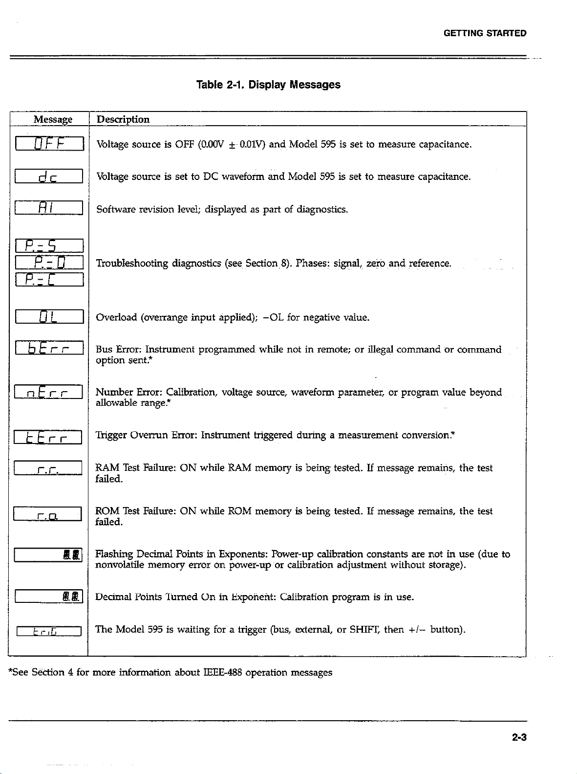
Table 2-l. Display Messages
GETTING STARTED
Message
lJF!-
dc
I
nr
I
ntrr 1
Description
Voltage source is OFF (O.OOV 5~~ O.OlV) ar@ Model 595 is set to measure capacitance.
Voltage source is set to DC wavefoim and Model 595 is set to measure capacitance.
Software revision level; displayed as part of diagnostics.
Troubleshooting diagnostics (see Section~B). Phases: signal, ze@ and reference.
Overload (overrange input applied); -0L for negative value.
Bus Error: Instrument programmed while not in remote; or illegal command or command
Dption sent?
Number Error: Calibration, voltage source, waveform parameter, or program value beyond
allowable range.*
ttrr
iI
I t
r.r.
r,rl
I-,,?
Trigger Ovemm Error: Instrument triggered during a measurement conversion?
RAM Test Fallure: ON while RAM memory is being tested. If message remains, the test
failed.
ROM Test Faihne: ON while ROM memory is being tested. If message remains, the test
failed.
Flashing Decimal Polnts~ in Exponents: Power-up calibration constants are not in use (due to
nonvolatile memory error on power-up ~01 calibration adjustment without storage).
Decimal Points Turned On in Exponefit: Calibration program is in use.
l%e Model 595 is waiting fork a trigger (bus, external, or SHIFT, then +I- button).
1
2-3
Page 24
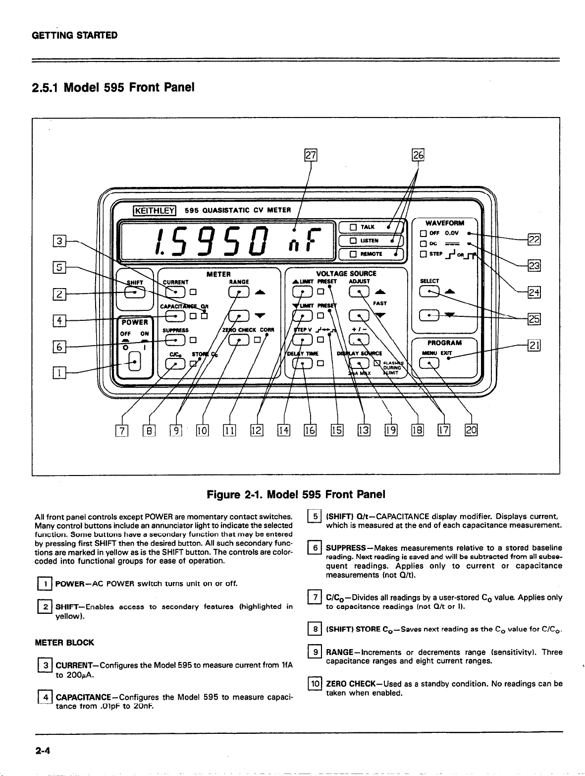
GETTING STARTED
2.5.1 Model 595 Front Panel
Figure 2-1. Model 595 Front Panel
All front panel controls except POWER are momentary contact switches.
Many control buttons include an annunciator light to indicate the selected
function. Some buttons have a secondary function that may be entered
by pressing first SHIFT then the desired button. All such secondary functions are marked in yellow as is the SHIFT button. The controls are colorcoded into functional groups for ease of operation.
1 POWER-AC POWER switch turns unit on or off.
cl
SHIFT-Enables access to secondary features (highlighted in
yellowl.
METER BLOCK
3 CURRENT-Configures the Model 595 to measure current from 1fA
cl
to 2oofi.
4 CAPACITANCE-Configures the Model 595 to measure capaci-
El
tance from .OlpF to 20nF.
2-4
-
w (SHIFT) Q/t-CAPACITANCE display modifier. Displays current,
which is measured at the end of each capacitance measurement.
6 SUPPRESS-Makes measurements relative to a stored baseline
q
reading. Next reading is saved and will be subtracted from all subsequent readings. Applies only to current or capacitance
measurements (not Q/t).
7 C/Co-Divides all readings by a user-stored Co value. Applies only
0
to capacitance readings (not
8 (SHIFT) STORE Co-Saves next reading as the Co value for C/Co.
q
9 RANGE-Increments or decrements range (sensitivity). Three
0
capacitance ranges and eight current ranges.
10 ZERO CHECK-Used as a standby condition. No readings can be
cl
taken when enabled.
Q/t
or I).
Page 25
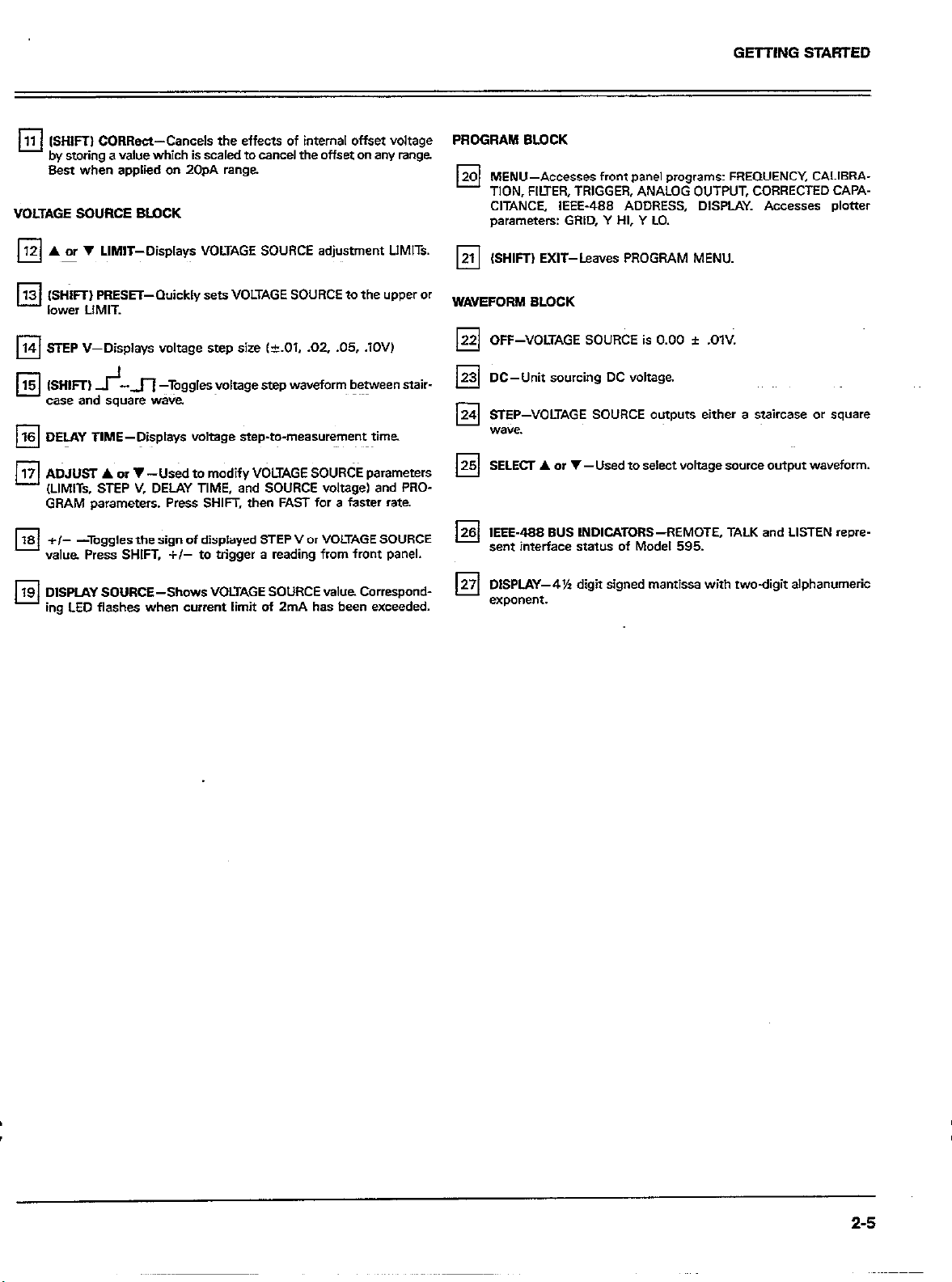
GETTING STARTED
(SHIFT) CORRect-Cancels the effects of internal of&3 VoltagE
Best when applied on 2OpA range
VOLTAGE SOURCE BLOCK
(SHIFT) PRESET-Quickly *en VOLTAGE SOURCE to the upper or
14 STEP V-Displays voltage step size t+.D1, .02. .05, .lOV)
cl
case and *qu*r* wave
ADJUST A or V-Used to modify VOLTAGE SOURCE parameters
(LIMIT*, STEP V, DELAY TIME, and SOURCE voltage1 and PROGRAM parameters. Press SHIFT, then FAST for a faster rate.
value Press SHIFT, +/- to trigger a reading from front panel.
18 DISPLAY SOURCE-Show* VOLTAGE SOURCE value Correspond-
cl.
tng LED fl**hes when current limit of 2mA has been exceeded.
a value which is scaled to cancel the offseX on any range
v LIMIT-Displays VOLTAGE SOURCE adjustment LIMITs.
fl
Tcggles~vcltage step waveform between stair.
;~
voltage step-to-measurement time.
the sign of displayed STEP V or VOLTAGE SOURCE
PROGRAM BLOCK
20 MENU-Accesses front panel programs: FREQUENCY, CALIBRA-
0
TION, FILTER, TRIGGER, ANALOG OUTPUT, CORRECTED CAPACITANCE, IEEE-488 ADDRESS, DISPLAY. Accesses plotter
parameters: GRID, Y HI, Y LO.
21 (SHIFT) EXfT-Leaves PROGRAM MENU.
III
WAVEFORM BLOCK
22 OFF VOLTAGE SOURCE i* 0.00 + .OlV.
III -
q DC-Unit sourcing DC voltage.
VOLTAGE SOURCE outputs either a staircase or *ware
25 SELECT . or V-Used to select voltage source outp”r waveform.
cl
28 ,EEE 488 8”s INDICATORS-REMOTE, TALK and LISTEN repre-
cl -_
sent merface status of Model 595.
27 DISPLAY-4% digit signed manti**a with two-digit alphanumeric
cl
exponent.
2-5
Page 26
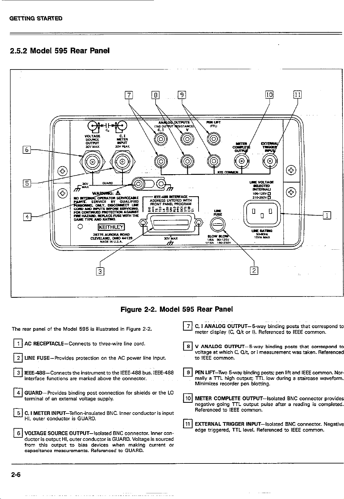
GEl-ilNG STARTED
2.5.2 Model 595 Rear Panel
Figure 2-2. Model 595 Rear Panel
The rear pand of the Model 595 is illustrated in Figure 2-2.
AC RECEPTACLE-Connects to three-wire line cord.
protection on the AC power line input.
3 IEEE-488-Connects the instrument fo the IEEE-488 bus. IEEE-488
q .
mterface functions are marked above the connector.
for shields or the LO
5 C, I METER INPUT-Tefloninsulated BNC. Inner conductor is input
q
HI, outer conductor is GUARD.
VOLTAGE SOURCE OUTPUT-Isolated SNC connector. Inner con-
from this wtpuf to bias devices when making current or
capacitance measurements. Referenced to GUARD.
output HI. outer conductor is GUARD. Voltage is sourced
2-6
7 C, I ANALOG OUTPUT-6way binding posts that correspond to
El
cl
q
10 MET!3 COMPLETE OUTPUT-Isolated BNC connector provides
q
11 EXTERNAL TRIGGER INPUT-Isolated SNC connector. Negative
q
~~~:~
meter display IC Q/t or Il. Referenced to IEEE common.
8 V ANALOG OUTPUT--B-way binding posts that correspond to
voltage at which C, Q/t, or I measurement was taken. Referenced
m IEEE common.
9 PEN LIFT-Two 5-way binding porn; pen lift and IEEE common. Nor-
mally a TTL high output; TTL low during a staircase waveform.
Minimizes recorder pen blotting.
negarwe gomg TTL output pulse after a reading is completed.
Referenced to IEEE common.
edge tnggered, TTL level. Referenced to IEEE common.
Page 27
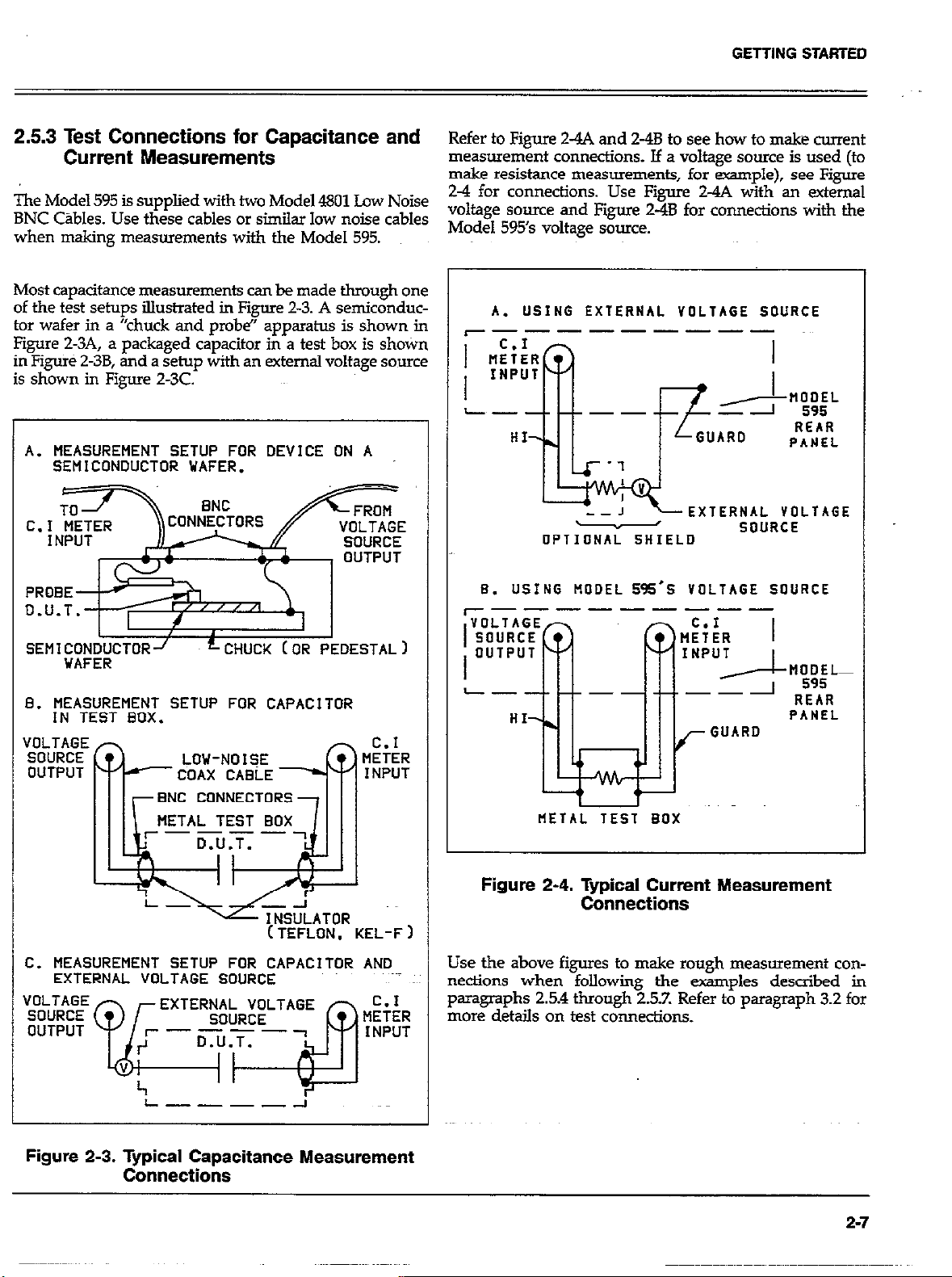
Current Measurements
The Model 595 is supplied with two Model 4801 Low Noise
BNC Cables. Use these cables or similar low noise cables
when making measurements with the Model 595.
Most capacitance measurements can be made through one
of the test setups illustrated in Figure 2-3. A semiconductor wafer in a “chuck and probe” apparatus is shown in
Figure 2-3A, a packaged capacitor in a test box is shown
in Figure 2-3B, and a setup with an external voltage source
is shown in Figure 2-3C.
A. MEASUREMENT SETUP FOR DEVICE ON A
SEMICONDUCTOR WAFER.
Refer to Figure 24A and 2-4B to see how to make current
measurement connections. If a voltage source is used (to
make resistance measurements, for -pie), see Figure
2-4 for connections. Use Figure 2-4A with an external
voltage source and Figure 2-48 for connections with the
Model 595’s voltage source.
A. USING EXTERNAL VOLTAGE SOURCE
~_--------
L- --
/-HOOEL
- - 595
REAR
PANEL
CONNECTORS
WAFER
8. MEASUREMENT SETUP FOR CAPACITOR
IN TEST BOX.
COAX CABLE
BNC CONNECTORS
METAL TEST BOX
C. MEASUREMENT SETUP FOR CAPACITOR AND
EXTERNAL VOLTAGE SOURCE
EXTERNAL VOLTAGE
OPTIONAL SHIELD
B. USING MODEL 595’S VOLTAGE SOURCE
c_--------
L- --
SOURCE
I
METAL TEST BOX
Figure 2-4. Typical Current Measurement
Connections
Use the above figures to make rough measurement connections when following the examples described in
paragraphs 2.5.4 through 2.53. Refer to paragraph 3.2 for
more details on test connections.
Figure 2-3. Typical Capacitance Measurement
Connections
2-7
Page 28
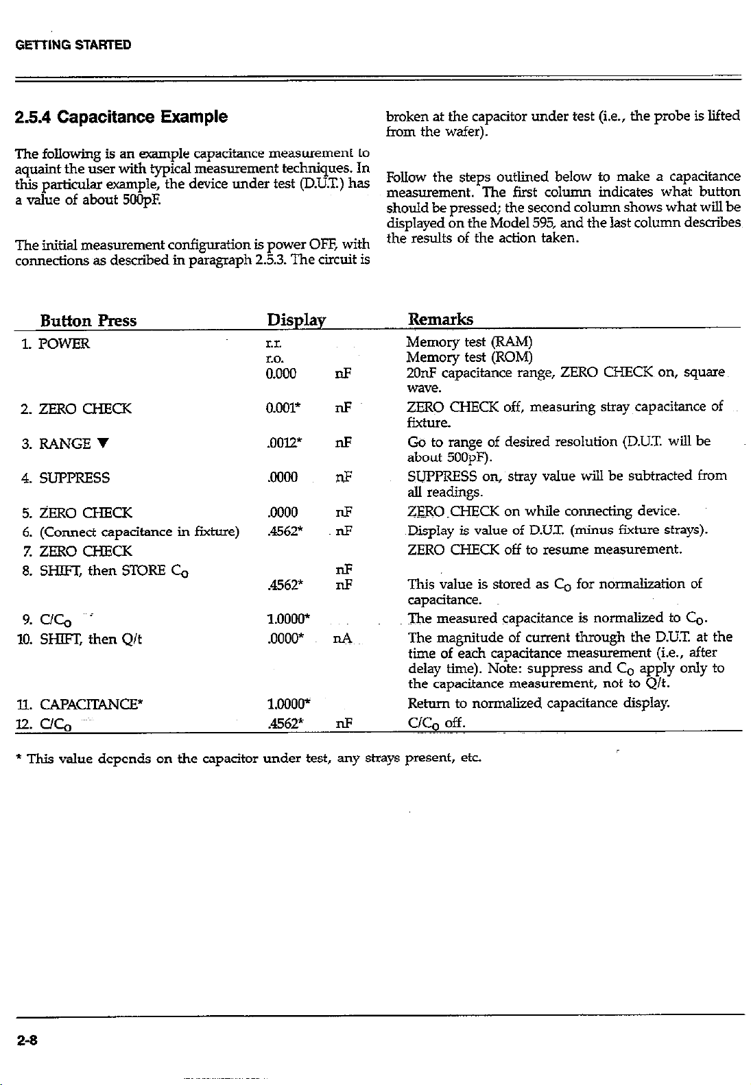
GElTlNG STARTED
25.4 Capacitance Example
The following is an example capacitance measurement to
aquaint the user with typical measurement techniques. In
this particular example, the device under test (D.UX) has
a value of about 5OOpE
The initial measurement configuration is power OFF, with
connections as described in paragraph 2.5.3. The circuit is
Button Press
1. POWER
2. ZERO CHECK
3. RANGE V
4. SUPPRESS
5. ZERO CHECK
6. (Connect capacitance in fixture)
7. ZERO CJFIECK
8. SHIFT, then STORE Co
9. UC, -~ 1.0000*
10. SHIFT, then Q/t
Il. CAPACITANCE* 1.0000~
12. UC, .4562* nF
Display
IT.
I.O.
0.000
O.OOT
.ool2=
.oooo
.oooo
.4562*
.4562*
.oooo*
IiF
IIF
broken at the capacitor under test (i.e., the probe is lifted
from the wafer).
Follow the steps outlined below to make a capacitance
measurement. The first column indicates what button
should be pressed; the second column shows what will be
displayed on the Model 595, and the last column describes
the results of the action taken.
Remarks
Memow test (RAM)
Memo6 test (ROMj
2018 capacitance range, ZERO CHECKS on, square
wave.
ZERO CHFCK off, measuring stray capacitance of
fixture.
Go to range of desired resolution (D.U.T. will be
about 500pF).
SUFT’RESS on, stray value will be subtracted from
all readings.
ZERO .CHECK on while connecting device.
Display is value of D.UX (minus fixture strays).
ZERO CHECK off to resume measurement.
This value is stored as Co for normalization of
capacitance.
The measured capacitance is normalized to C&
The magnitude of current through the D.U.T at the
time of each capacitance measurement (i.e., after
delay time). Note: suppress and Co apply only to
the capacitance measurement, not to Q/t.
Return to normalized capacitance display.
UC0 off.
* This value depends on the capacitor under test, any strays present, etc.
2-8
Page 29
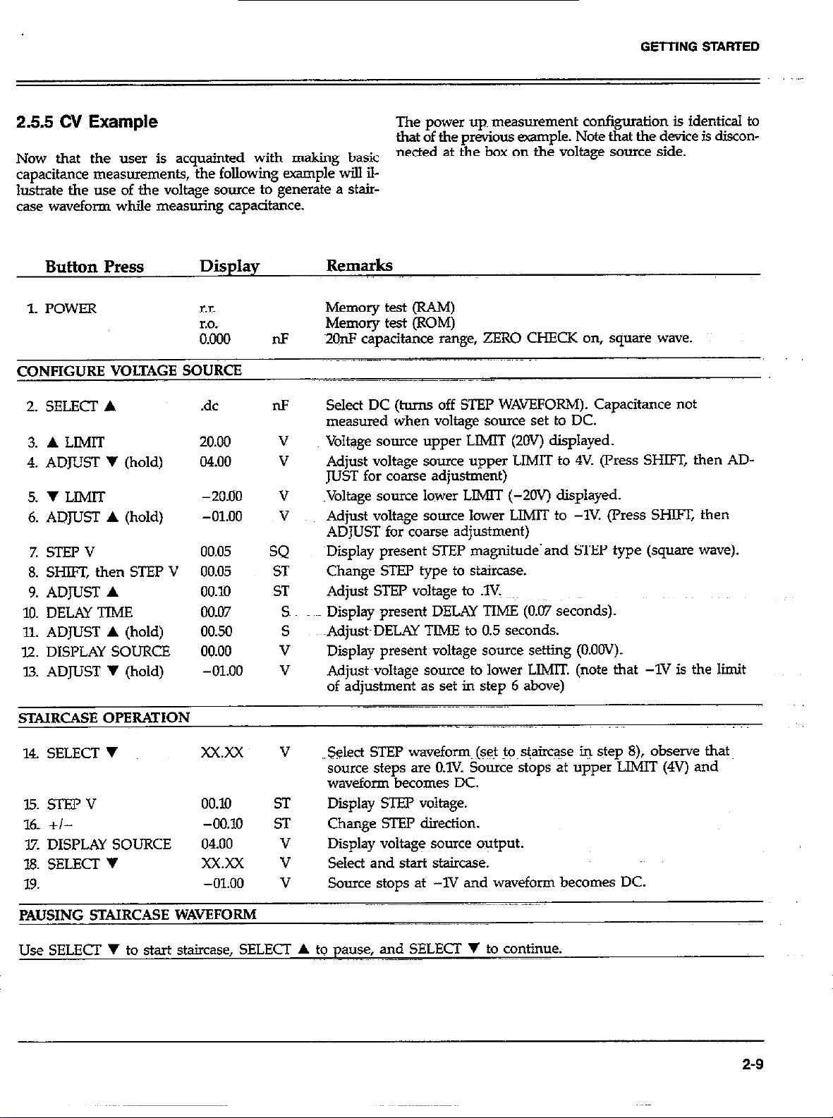
GETTING STARTED
,...
2.5.5 CV Example
Now that the user is acquainted with making basic
capacitance measurements, the following example will illustrate the use of the voltage source to generate a staircase waveform while measuring capacitance.
Button Press
1. POWER
CONFIGURE VOLTAGE SOlJIb
2. SELECT A
3. A LIMIT
4. ADJUST ‘I (hold)
5. v LIMIT
6. ADJUST A (hold)
z STEPV
8. Sm, then STEP V
9. ADJUST A
10. DELAY TIME
11. ADJUST A (hold)
12. DISPLAY SOURCE
I.3 ADJUST v (hold)
Display Remarks
IX Memory test (RAM)
LO. Memory test (ROM)
o.ooo IIF 2C!nF capacitance range, ZERO CHECK on, square wave.
.dc
Select DC (tmns off STEP WAVEFORM). Capacitance not
measured when voltage source set to DC.
20.00
04.00
Voltage source upper LIMIT (20V) displayed.
Adjust voltage source upper LIMIT to 4V. (Press SHIFT, then AD-
JUST for coarse adjustment)
-20.00
-01.00
~Voltage source lower LIMIT (-2OV) displayed.
Adjust voltage source lower LIMIT to -lV. (Press SHIFT then
ADJUST for coarse adjustment)
00.05
00.05
00.10
00.07
00.50
00.00
-0l.00
~Display present STEP magnitude‘and STEP type (square wave).
Change STEP type to staircase.
Adjust STEP voltage to .lV. ~~~
Display present DELAY TIME (0.07 seconds).
~Adjust~DELAY TIME to 0.5 seconds.
Display present voltage source setting (O.OOV).
Adjust voltage soUTCe to lower LIMIT. (note that -lV is the limit
of adjustment as set in step 6 above)
The power ups measurement configuration is identical to
that of the previous example. Note that the device is disconnetted at the box on the voltage source side.
STAIRCASE OPERATION
14. SELECT v
xX.xX v $&xt STEP waveform (set 10~ s@ircgse in step 8), observe that
source steps are O.lV. Source stops at upper LIMIT (4V) and
waveform becomes DC.
15. STWV
16 +I-
17. DISPLAY SOURCE
7.8. SELECT v
19.
PAUSING STAIRCASE WAVEFORM
00.10 ST Display STEP voltage.
-00.10 ST Change STEP direction.
04.00
V
Display voltage source output.
xX.xX v Select and start staircase.
-01.00 v Source stops at -lV and waveform becomes DC.
Use SELECT v to start staircase, SELECT A to pause, and SELECT v to continue.
2-9
Page 30
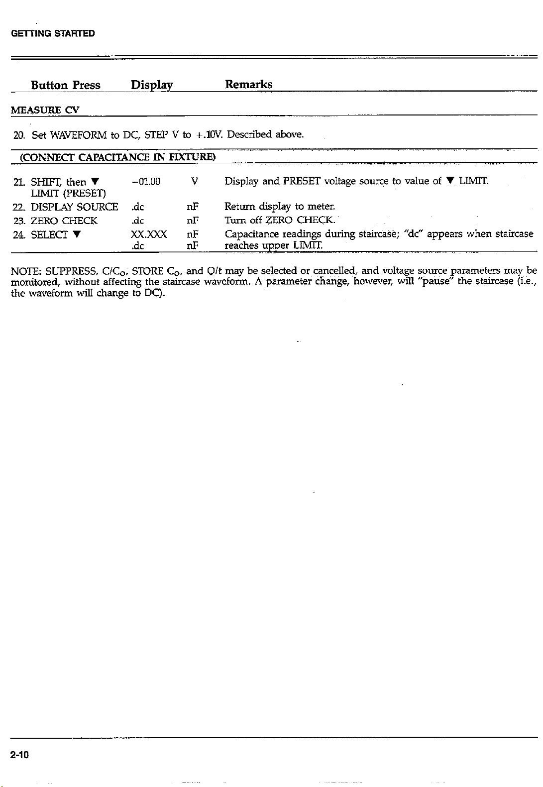
Button Press
Display
Remarks
MEASURE CV
20. Set WAVEFORM to DC, STEP V to +.lOV. Described above.
.~, ..~..~..~~_
(CONNECT CAPACITANCE IN FitiRE)
21. SI-EFT, then v
-a.00
V Display and PRESET voltage sourc$ to value of r LIMIT.
LlMlT (PRESET)
22. DISPLAY SOURCE .dc
23. ZERO CHECK
24. SELECT v
.dc nF
xX.xXx nF
.dc
nF
III
Return display to meter.
Turn off ZERO CHECK.
Capacitance readings during staircase; “dc” appears when staircase
reaches upper LIMIT
NOTE: SC’PPRESS, C/Co; STORE Co, and Q/t may be selected or~c%nceJlecJ, and voltage source parameters may be
monitored, without affecting the staircase waveform. A parameter change, however, will “pause” the staircase (i.e.,
the waveform will change to DC).
2-10
Page 31

The following is an example of a typical current measure-
ment. This example uses a lM0 resistor in a test-box. See
Figure 2-4 for measurement connections. The voltage source
is set to 1V to cause l& input current to flow
(I = IVIIMQ).
GETTING STARTED
The initial measurement configuration is POWER off, with
input cables attached to the Model 595. The input circuit
is Temporarily disconnected at the test box, on <he voltage
source output side.
Button Press
1. POWER
2. CURRENT
3. RANGE v
Display Remarks
r.r.
CO.
0.000
-.OOOT
-0.OOT
0.000
.oooo
IIF
IL4 Place unit in CURRENT function.
PA
Memory test (RAM)
Memory test (ROM)
~2OnF capacitance range, ZERO CHECK on, squtie wsVe.
Seth unit to 2OpA range.
Corrects for internal offsets.
Go to RANGE of desired resolution (press five times for this
example).
CONNECT RESISTOR)
6. SELECT A
Z DISPLAY SOURCE
.oooo
00.00
~P-4
V Displays voltage sourced.
Select DC WAVEFORM.
~~ v Adjust voltage source to 1V out.
9. DISPLAY SOURCE .oooo
10. ZERO CHECK
.9835*
fi Return unit to meter display.
~~ la
Read value from display.
* This value depends on the resistor under test, stray currents, etc.
Variation: Also try using SUPPRESS on readings and adjust voltage source to 1.5V.
2-11
Page 32

GETTING STARTED
2.5.7 IV Example
of CV -pie in paragraph 2.5.5. Then perform the steps
described below. (NOTE: This example is based on the
Setting up !n IV measurement is, for the most part, quite
sim&u to setting up a CV measurement. Follow steps l-20
Button Press Display
same measurement configuration described in paragraph
2.5.6.)
Remarks
MEASURE IV
1. CURRENT
-0.002 nA
,Place unit in CURRENT function (then press RANGE A to
put~instrument to appropriate range; in this case, the 2Ofi
range).
(CONNECT RESISTOR)
2. SHIFT; then V LIMIT
3. DISPLAY SOURCE
4. ZERO CHECK
5. SELECT V
-01.00
O.LlOT
-1.0158*
V :~7X@I$y and PRESET the voltage source.
~~$4
@’
xx.xxx pA
Return display to meter.
Turn off ZERO CHECK.
Current readings during staircase; constant DC readings
when staircase reaches upper LIMIT,
XThis vaIue depends on resistor under test, stray currents, etc:
2-12
Page 33

SECTION 3
OPERATION
3.1 INTRODUCTION
Detailed front panel operation of the Model 595 is desaibed
in this section, including test connections and complete
front and rear panel descriptions in the f&t half (Part l),
and how to make Cv, IV and Q/t-V plots is described in
the second half (Part 2). Many of these operations can also
Fo,p’qugrammed mer the
IEEE&B bus, as desaibed in Sec-
PART 1
Front and Rear Panel Descriptions
3.2 TEST CONNECTIONS
The following paragraphs will describe how to set up
Model 595. Connections can be made with the supplied
Model 4801 cables; in addition, other low noise, coaxial
BNC cables may be used with the Model 595. In any con-
nection to this inshurnent, it is advisable to use the shortest
cables practical for the particular test setup. In situations
where vibration may be present (such as a vacuum pump),
tape the cables to a stable object to avoid excessive vibra-
tion and electrical noise. Note: see warnings in paragraph
2.5 before operating instrument.
Packaged capacitors should also be measured in a shielded
metal box and are connected as ikstmted in Figure 3-1B.
A. MEASUREMENT SETUP FOR DEVICE ON A
SENICDNDUCTDR WAFER.
CONNECTORS
SEMICONDUCTOR’
WAFER
8. MEASUREMENT SETUP FOR CAPACITOR
IN TEST BOX.
VOLTAGE
%E
ENC CONNECTORS
L CHUCK t OR PEDESTAL )
METAL TEST BOX
3.2.1 Capacitance Connections
Many applications of the Model 595 will involve using the
instrument to determine capacitance of devices on semiconductor wafers. A variety of probe station setups are
available; the preciseconfiguration of such a station is up
to the user, depending on his needs and equipment
available to him. However, most of these setups wiU use
connections similar to those illustrated in Figure 34.A with
the test fixture completely enclosed in a light-tight metal
box for electrical shielding. The metal box should be~<qpnetted to GUARD. Note that the Model 595 VOLTAGE
SOURCE OUllWT is connected to the substrate (to
( TEFLON. KEL-F)
C. MEASUREMENT SETUP FOR CAPACITOR AND
EXTERNAL VOLTAGE SOURCE
L
L-----t
Figure 3-l. Capacitance Measurement Connections
3-l
Page 34

3.2.2. Connections for Current Measurements
The Model 595 is capable of making current measwetients
in addition to capacitance measurements.
Although current measurements may not require the use
of a voltage source, the current function cam be used with
the voltage source to dete-e a resistance value @y oh&
Law, V=IR) or to generate IV curves.
3.3 DETAILED FRONT PANEL CONTROL DESCRIPTIONS
This section gives complete descriptions of all Model 595
front panel controls. Note that the front panel buttons are
arranged and characterized by color-coded “blocks’-
METEKblock, WA~CXM block, VOT,X&E SOURCE
block, and pROG&W block. The Sm button is used
to access second functions, which are lab&d in yellow.
Figure 3-2A Illustrates a typical current measurement setup
with an external voltage, and Figwe 3-28 shows a standard
circuit using the instrument’s internai voltage source.
Again, low noise coaxial BNC cables and a metal test box
to shield the device should be used for best results.
A. USING EXTERNAL VOLTAGE SOURCE
----------
w
-
OPTIONAL SHIELD
USING HODEL 595’S VOLTAGE SOURCE
El.
__..___ -----~~
EXTERNAL VOLTAGE
SOURCE
METER Block
The following controls are found in the METER block of
the Model 595 front panel.
3.3.1 CURRENT
The CURRENT button places the Model 595 in the current
measurement function. The indicator light next to the button is on when this function is selected. Any one of eight
ranges (2OpA to 2004 may be used with this function.
3.3.2 CAPACITANCE
The CAPACITANCE button places the Model 595 in the
capacitance measurement function. The red indicator light
is .on when this function is selected. There are three
capacitance ranges: 2OnF, 2nF and 200pF.
When making a capacitance measurement, the Model 595
makes three charge measurements around the voltage
source “step” (the STEP waveform must be selected). See
Figure 3-3. From these three charge measurements the
capacitance and the current through the device (at the end
of the delay time) are calculated. The voltage reported with
the reading is the source voltage (V,) plus half of the step
voltage.
-PANEL
I
tlETAL TEST BOX
Figure 3-2. Connections for Current Measurements
3-2
Q/t displays the current flowing through the device at~the
end of the delay time. This is selected by pressing SHIFJ
then the CAFACIIIWCE Q/t button. Note: the capacitance
function must be selected to select Q/t. The yellow indicator
light is on when the Q/t current is being displayed.
Page 35

I
RELEASE
INTEGRA’TOR
OISCHARGE
cx -sg” o/t-y
INTEGRATOR
OPERATION
When the SW~RJZ$S button is pressed, ~JI: instrument
&ill store the next mea&rement as a baseline. The SUPPRESS indicator light will illuminate. Au subsequent
readings taken will be the difference between the measured
value and the stored baseline.
The baseline maintains its absolute value regardless of
range. For example, if a O.lnF signal is suppressed on the
2nF range, it will remain at O.lnF on the 2OnF and 2OOpF
ranges. Only one reading for the presently selected function can be suppressed; the value will be lost if the function is changed. The instrument can be toggled between
Q/t and capacitance without losing the stored value.
(O/t)(DELAY TIME+t,)
CX( CCIRRECTED I - cx -
Figure 3-3.
READING VOLTAGE=V+ISTEPV
Integrator Charge vs Time Curve
STEPV
1 z ~-~~-
for
a 30
Capacitance Measurement
C/Co allows the user to normalize capacitance to a stored
capacitance value (Co). c/c, applies only to the capacitance
reading (even while Qk is being displayed). To store a
capacitance reading (Co), simply set up- the desired
capacitance measurement, then press SHIFT then STORE
&. The next reading will be stored as Co. To normalize
the capacitance readings to Co, prks C/Co (the LED will
come on). This will divide a!J subsequent readings by the
stored reading, Co, and show the resulting quotient on the
display. Once a value of Co is stored, it will be retained
in memory until a new value is stored or the instrument
is turned off.
C/Co allows comparison of the relative shapes of two or
more CV curves even when absolute capacitance values
may be different.
3.3.4 SUPPRESS
The suppressed readings can be as small as the resolution
of the instrument will allow, or as large as full range (see
Note 1). Some typical examples indude:
Applied Suppressed
~~ -.~Signal Reading
pF 0.5 pF
- 1.5
IIA -1 l-IA
11.3 nF
l3nF
O.lOpA - O.OlpA
Displayed
Valila
29.5 pF
- 0.5 nA
- 1.7 Is
OSlpA
NOTES:
1. Using suppress reduces the dynamic range of the
measurement. For example, if the suppressed value is
lOO.OOpA on the 2OOpA range, an input current of more
than 99.99pA would overrange the instrument even
though input currents up to 199.99pA are normally
within the capabilities of the 2COpA range.
2. Setting the range lower than the suppressed value will
overrange the display; the instrument will display the
“OL” message under these conditions.
3. To store a new baseline, suppress mu&first be disabled
and then enabled once a&n. The next reading taken
will be stored as the n&baseline.
4.
Enable suppress on the measurement range that yields
the highest resolution for the application.
5. If the ins&ument is displaying Q/t when suppress is
enabled, the capacitance value will be suppressed even
though the caiacitance reading is not dkslayed. Suppression has no effect on Q/t readings.
The SUPPRESS button allows the user to compensate for
external offsets present in the test setup by subtracting the
3.3.5 ZERO CHECK and CORRect
offset value from subsequent readings. (To compensate for
internal offsets, see~ZER0 CHECK and CORRect.) Sup-~- zero che& is -d to protect the input amplier of the
Press~maY be used with capacitance or went measure-
men& but not Q/t.
~Model595 from overloads and switch@g transients when
changing instrument functions or connections to the devices
3-3
Page 36

under test. Therefore, make sure the ZERO CHECK in-
dicator light is on when changing functions or connections.
The ZERO CHECK button toggles the instrument in and
out of zero check.
The RANGE A, v buttons in the METER block of the
Model 595 allow the user to increment or decrement the
range. The A range button selects the next higher range
and the ‘I button selects the next lower range.
Zero check is also used with zero correct to cancel internal
offsets in the Model 595 input amplifier. Zero correction
is not applicable to capacitance or Q/t but should be performed for the current function on the 20pA range.
Note that the specifications at the front of this manual
assume that the instrument has been properly zeroed. The
following procedure should be used after the instrument
has warmed up for two hours and repeated as needed every
24 hours or if the ambient temperature changes by more
than PC.
1. Select the current function and the 2OpA range.
2. Press the ZERO CHECK button and be sure the ZERO
CHECK indicator light is on. The Model 595 input
amplifier is now configured to read its own internal
offset.
3. Pr.ess SHfFJ then CORRect to zero correct the instrument. Note that if zero check was not enabled, the zero
correct operation will enable zero check first.
4. The proper range may now be selected and ZERO
CHECK released to make a measurement.
NOTES:
1. Remember to leave zero check enabled when connecting or disconnecting input signals, or when changing
ranges or functions.
2. The zero correct value is stored in permanent memory
and is maintained while the instrument is turned off.
A new zero correct value always replaces an older one.
WAVEFORM Block
The following controls are found in the WAVEFORk block
of the Model 595 front panel. The SELECT A, v buttons
are used to select the voltage waveform.
The Model 595 is capable of sourcing either DC or a stepped
voltage to the device under test. At power up, the Model
595 is set to measure capacitance, and the waveform is set
to square wave.
OFF CLOV
OFF sets the voltage source to O.OOV iO.OlV. This can be
used to set the voltage source to zero without having to
use the ADJUST buttons. If capacitance is selected, an
“OFF” message will appear on the display since a step is
necessary to measure capacitance.
DC
When DC is selected, the voltage source will output a constant voltage, equal to the voltage source programmed
value. If the capacitance function is selected, the “DC’
message will appear on the display since a step is necessary
to measure capacitance.
STEP
3.3.6 RANGE A, v
The Model 595 has several ranges available for both
capacitance and current measurements. The capacitance
ranges are 2OpR ZnF and 206 The current ranges are 2OpA,
2OOpA, 2nA, ZOnA,2OOnA, 2pA, 206 and 2004. The instrument powers up on the 2OnF capacitance range.
When making a measurement, choose the lowest range
possible without overloading the Model 595. This win maximize measurement resolution.
3-4
The STEP waveform is the fundamental signal required for
capacitance measurements. Two STEP waveforms are
available: square wave and staircase. The characteristics of
this waveform are tailored using the controls within the
VOIXAGE SOURCE block.
The instrument~powers up with square wave selected.%
is the waveform used to measure capacitance at a specific
test voltage. Refer to Figure 3-4 for a diagram of the
waveform. The voltage starts at VI (set by the user in the
range of -20 to +20 volts). After the programmed delay
Page 37

OPERATION
time (plus 0.04sec) the voltage changes by STEP V. The outO.Okec) and then returns to the original Vl level. The out-
put voltage continues to repeat the above process. For
capacitance measurements, the reading voltage is reported
as V, +~ 1% V,, For current measurements the reading
is reported at the voltage where the measurement was
made.
Staircase is selected in the same way as square wave. The
timing~is also the same but at the end of the second delay
time the waveform does not return to VI. Instead, it increments again by STEP V to VZ. This results in an output
voltage waveform that resembles a staircase-continually
increasing (or decreasing) uniformly in steps. When the
output voltage reaches the upper or lower limit, the output voltage will switch to DC. To restart a staircase
waveform, set the voltage source output to the desired startine voltage (the “ores&’ feature makes this easv) and re-
se&t the&p waveform.
r---V2
t STAIRCASE
3.3.7 A LIMIT, v LIMIT, and PRESET
The A LIMIT and ‘I LlMIT buttons set the maximum and
minimum voltage that the voltage source will output. These
limits may be set by the user to protect a device that could
be damaged by excess voltage. On power up the A LIMIT
is set to +u) volts and the 7 LIMIT to -20 volts. These
power up limits are the maximum and minimum voltages
that the limits can be set to.
When a LlMlT button is pressed, the display shows that
voltage limit. The ADJUST buttons are used to change that
limit in 1OmV increments.
An a- function of the voltage limit buttons is PRESET.
PRESET allows the user to quickly set the output voltage
value to the maximum or minimum limit without having
to use the ADJUST buttons. To use PRESET, press SHIFI,
then A LIMIT or v LIMIT.
3.3.8 STEP V
When a step waveform is selected, STEP V determines the
step size (the small incremental change in voltage) and
whether the waveform will be a square wave or a staiiase.
The .step size may be O.OlV, O.O2V, O.O5V, or O.lOV with a
positive or negative polarity. On power up, the step voltage
is set to +O.O5V square wave. Detail descriptions of the
voltage waveform may be found under WAVEFORM
BLOCK - STEP.
Figure 3-4. Voltage Output Waveform
VOLTAGE SOURCE Block
The Model 595 has a built-in voltage source that is used
to make capacitance measurements. It can alsa be used with
the current function for measuring IV characteristics of
devices. The output voltage may be set from -2OV to +ZOV
in IOmV increments. Limits may be set to prevent the output from exceeding a selected value. The maximum~current for which the output voltage is guaranteed is 2mA and
current limiting prevents the output current from exceeding
4mA even into a direct short.
The following controls are found in the VOLIAGE SOURCE
dicate which parameters are displayed. Press to select a pardisplay.
To select the step voltage, press STEP V. The indicator light
will be on while the step voltage is displayed. Use the
ADJUST buttons to select the step size. The * button may
also be used to change the polarity of the step voltage.
Press SHIFT then STEP V to toggle the waveform between
square wave and staircaseSquare wave and staircase are
shown pictorially next to the STEP V button.
3.3.9 DELAY TIME
The time from the voltage step to the fmal charge measure-
ment for a capacitance calculation, or from the step to the
measurement in current, is the delay time. Delay time is
used to allow the device under test to respond to the change
in voltage before measurement. The delay time is not usually critical when performing simple capacitance or IV
measurements. It is important when performing capacitance and CV measurements on MOS capacitors.
3-5
Page 38

To change the delay time, press DELAY TIME, then the
ADJUST A , ‘I buttons to increment or decrement the
time. The delay time can be set from 0.07sec to 199.99sec.
On power up, the delay time is set to 0.07sec.
‘:
Figure 3-3 shows in more detail where the delay time occurs. The total time of the voltage step is delay time plus
Tl. Tl is the period necessary for the Model 595 to finish
the measurement, and is typically 0.04sec (see specification clarifications at the front of the manual). The total time
of the voltage step (delay time plus TI time) is called the
step time.
Another time period important to the capacitance function
is T, . This is the time period from the middIe of charge
measurement Q2 to the middle of charge measurement Q3.
The time period T, is 1/8th of the delay time, with a
minimum time of 44msec. These two charge measurements
are used to calculate the current flowing though the device
under test (Q/t). The expression for Q/t is found in Figure
3-3. 7
displayed. This light will flash when the output voltage cur-
rent limit becomes active. The voltage source is capable of
outputting 2mA, after which the output voltage will begin
to change and not match the voltage source setting. The
current limit will prevent the output current from exceeding
4mA.
3.3.11 ADJUST A , V
The voltage source ADJUST buttons are used to increase
or decrease the values of A LIMIT, v LIMIT, STEP V,
DELAY TIME and the programmed output voltage. To
quickly adjust these voltage source parameters, press
SHIFT, then the appropriate ADJUST button. Note that
while readings are being displayed, pressing either of the
ADJUST buttons will change the programmed output
voltage.
NOTE
The ADJUST buttons are also with front panel pro-
grams. See paragraph 3.4.
3.3.10 DISPLAY SOURCE
The DISPLAY SOURCE button causes the Model 595 to
display the programmed output voltage. On power up, the
Model 595 is programmed for 0.00 volts.
To view the programmed output voltage, press the
DISPLAY SOURCE button. To change the voltage, press
the ADJUST A or ADJUST v button to increase or
decrease the programmed output voltage.
The +/- button may be used to change the polarity of the
voltage (while displayed). The programmed output voltage
may be quickly set to the voltage limits by pressing SHIFT,
then the A LIMIT or v LIMIT button for the maximum
liiit or mirii~mum limit, respectively.
The indicator light adjacent to the DISPLAY SOURCE button is on when the programmed output voltage is being
3.3.12 +I-, Front Panel Trigger
The +I- button of the Model 595~allows the user to change
the polarity of the voltage source while the programmed
output voltage is being displayed. It can also be used tom
change the polarity of STEP V while STEP V is displayed.
A secondary feature of the +I- button is that it can be used
as a trigger source from the front panel when another trigger source is not available (press SHIFT, then +I-). See
paragraph 3.4.4 for information on triggering.
3.4 FRONT PANEL PROGRAMS
The Model 595 has several capabilities that are accessed as
“front panel programs”. These programs operate through
the MENU button. To scan the availableprograms, simply
press MENU. Each additional press of the MENU button
will move the menu to the next program. To exit, press
SHIFT, then EXK Table 3-l lists the available front panel
programs.
3-6
Page 39

Table 3-1. Front Panel Programs
OPERATION
l-r-
I* $ Frequency
7R/ *$ Calibration
FI I k
Erg,
lZELZ3 Ana1og Output
rfHP
I
IEFt
] Filter
1 Trigger
1 Corrected Capacitance Corrects capacitance readings for error currents. l=correction on,
* IEEE-488 Address
Powers Line frequency setting. Fr=5OHz, Fr=60Hz
Allows calibration of instrument.
Selects ffiter O-3, see section 3.4.3
Trigger mode: O=continuous, l=one shot
C, I voltage at rear panel ANALOG OUTPUT binding posts.
O=correction off. See Section 5.34 before using.
IEEE-488 Address Selection Program.
l-l IclP
[ L1 H I ?]tYHIGH
y J o-r’It YLOW
I-,
* Stored in permanent memory.
t Appears in MENU only when address code 42, 43 is selected.
S~Appears in MENU only when calibration is enabled.
) * Display
It Grid Sets and plots grid for IEEE-488 data graphing.
Sets numeric or alpha exponent.
Plotter Y-axis high limit.
Plotter Y-axis low limit.
3-7
Page 40

OPERATION
3.4.1 Power Line Frequency
The line frequency program is used to set the Model 595
to the available line frequency (either 50 or 6OHz). This pro-
grams is accessed as part of the calibration procedure and
is discussed in Section 7. During normal operation this front
panel program will not appear in the MENU.
3.42 Calibration
An advanced feature of the Model 595 is digital calibration.
The instrument can be calibrated from the front panel or
over the IEEE-488 bus. To use front panel or IEEE-488 bus
calibration, refer to the calibration procedures outlined in
Section Z During normal operation this front panel pro-
gram will not appear in the MENU.
3.4.3 Filter
The Model 595 has three digita filters that can be used to
minimize the effects of noise on individual measurements
and plotted curves. To use the ftiter program, press the
MENU button until “FlLt” appears~ on the display. Next to
“FILt” is a. number. If the number is zero, then the filter
is off, -and the actual unmodified curve will be plotted. To
advance to a higher level filter, press the voltage sourc$ A
ADJUST button. To decrease a filter level, press the~voltage
source V ADJUST button. To exit from the program, press
SIGT and then EXIT.
The suitability of each of these for “curve smoothing”
should be determined by considering the number of
measurements cr samples in the curve; specifically, the fundamental portion to be studied (region of interest).
Filter 1 is used when there are 20 or more samples in the
fundamental change area of the curve. This filter provides
minimal smoothing of the curve. Filter 2 should be used
when there are 50 or more samples in the fundamental portion of the curve for maximum curve smoothing. Lastly,
filter 3 is available to smooth slowly changing DC signals
(or curves with more than 200 samples in the fundamental portion). This filter should normally only be used with
DC signals since it would distort most CV or lV curves.
Figure 3-5, shows an example of proper and improper use
of a filter on a cmve with 60 readings in the region of interest. Notice the distortion of the curve using Filter 3.
An important characteristic of each filter is its “window”.
Each filter takes the weighted average of a certain number
of readings. This average is symmetrical about the middle
reading. Filter 0 (when filter is “off’? has a one reading window, Filter 1 has a three reading window, Filter 2 has a nine
reading window, and Filter 3 has a 24 reading window.
The weightings (oi coefficients) assigned to each reading
are as follows:
Level 1: 114, 112, 114
Level 2: -1132, l/32,1/8, 15i64, 9i32, W64, I@, 1132, -1132
Level 3: l/32, l/32,1132, l/32, 1132, 1132, 1132, 1132, l/16, 1116,
1116, 1116, l/16,1/16, 1116, 1116, l/32,1/32, 1132, ‘JJ32,
1132, l/32, 1132, 1:32.
Figure 3~-6 illustrates~ the coefficients of Filter 2.
3-8
Page 41

OPERATION
Figure 3-5. Example: Using the Filter on a MOS Device Curve
3-9
Page 42

SIN FUNCTION
Curves plotted with filter 0 will start plotting one reading
after it starts staircasing, filter 1 will begin plotting two
readings later, filter 2 will begin five readings later, and filter
3 wiU begin I3 readings later. Similarly, these filters will
finish early by the same number of readings, leaving an
unplotted region at the end.
COEFFICIENTS
/
CENTER READING
Figure 3-6. Coefficients in Filter 2
The coefficients are chosen to approximate the Fourier components of a brick wall filter [(sin X)/X]. The passband of
the filter is chosen to pass the signal curve while attenuating
noise outside the passband. Typical white noise reduction
is as follows: Level 1, 1.7; Level 2, 2.5; Level 3, 5.0.
Since the filter is symmetrical, there is a delay between
what is displayed (middle reading) and the measurement
being taken. Filter 0 has a one reading delay, filter 1 has
a two-reading delay, ftiter 2 has a five-reading delay, and
filter 3 has a Breading delay.
If a meter or voltage source parameter is changed, the filter
is “cleared” and starts over. Changes in step~size, delay time,
filter type, trigger mode, voltage limits, voltage souxe, function and range will restart the filter. (The only parameters
that don’t affect filter operation are C/Co, STOREC~;~~Q/t~
and SUPPRESS). The filter is cleared during OL readings
and while zero check is on, for fast reading respon&
3.4.4 Trigger
A “trigger” is a stimulus to the Model 595 to begin a
measurement. Triggering may be done in two basic ways:
continuous or one-shot. In continuous, the stimulus starts
a series of measurements. In one-shot trigger, a single
measurement will be processed each time a trigger stimulus
is received. On power up, the Model 595 is in continuous
trigger and the stimulus is internally generated to start the
measurements.
To access the trigger mode from the front panel, press the
MENU button until the message “triG” appears on the
display. Next to “triG” a 0 or 1 appears. Zero signifies that
the instrument is in continuous trigger and 1 signifies oneshot trigger. To change trigger functions, press either one
of the voltage source ADJUST buttons to toggle the trigger
mode between 0 and 1. After the desired trigger type-is
displayed, exit from the program by pressing Sm, then
EXIT.
To send the instrument a trigger from the front panel, press
SHIFT. then +I-.
The Model 595 can also respond to other trigger stimuli
besides the button sequence from the front panel. The rear
panel has an external trigger input connector (see
paragraph 3.5.1) and various commands over the IEEE-488
bus can be used as a trigger stimulus (see paragraph 4.9%).
When the filter is first enabled or starts over, there is an
initial reading delay. Each location in the filter is initiaIly
ftied with the fit reading and subsequent readings pass
through the filter. This can be seen on plotted curves.
3-10
NOTE: The button sequence, SHIFT, +I-, will always
generate a trigger mess the front panel operation is locked
lout from the IEEE-488 bus.
Page 43

ne analog output program allows the user to set the C
I analog output gain to Xl or X10. Xl is used for readings
over 10% full range. With a maximum input of i19999
counts, output is &V (This is equivalent to 1V on output
for 10,000 counts on the display). X10 is used for readings
less than 10% of full range. With a maximum input of &ZOO0
counts, output is K2.V. (This is equivalent to 1V output for
IOOO~coUnts on the display).
OPERATION
ditions for equilibrium and proper use of the capacitance
correction program.
To use this program, press the MFNU button until “cC4P”
is displayed. A 0 signifies that correction is off, and 1 means
that corrected capacitance has been enabled. To toggle corrected capacitance on or off, simply press either of the
voltage source ADJUST buttons. Note that the Model 595
always powers up with corrected capacitance off.
To access the analog output program, press MENU until
“Aout” is displayed. A message of “Aout 1” means gain is
Xl; “Aout 10” means gain is X10. Press either of the voltage
source ADJUST buttons to toggle the gain between Xl and
XlO.
The analog output signal is available on the rear panel
ANALOG OUTPUT connector, and follows the C, I or Q/t
display
Notqthat the selected analog output gain is not~~sayed when
the instrument is turned off. When the Model 595 is
powered on again, the gain will default to Xl.
3.4.6 Corrected Capacitance
Thii program allows the capacitance reading to be corrected
for the effects of leakage currents. It must be determined
that the device under test has completely responded to the
change in voltage used in the measurement and that the
Q/t current is only related to DC errors such as leakage current or low oxide resistance. In these cases, CORRECTED
CAPACITANCE uses the Q/t measurement to cancel the
effects of these DC error currents on the-capacitance
reading. The capacitance is then calculated by:
(Q/t)(delay time + tl)
Cx (corrected) = Cx -
step v
3.4.7 IEEE-488 Address
Selection of the IEEE-438 address function is indicated by
the following menu message:
IEEE 28
Along with the message, the presently programmed
IEEE-488 address (28 in this example) will be displayed. To
change the value, use the voltage source ADJUST A , v
buttons. When the desired value is shown on the display,
press SHIFT, then m to return to normal operation. Addresses 0 to 30 are the normal IEEE-488 addresses. Codes
40 and 41 allow the Model 595 to control an IEEE-488
printer. Codes 42 and 43 allow the Model 595 to control
an IEEE-488 plotter. For complete information on controlling the Model 595 over the IEEE-488 bus, refer to Section
4. For plotter and printer information, see paragraph 3.9
and 3.11.
NOTE
When actively outputting data while set to codes
40-43, the Model 59.5 acts as a controller, and by
IEEE-488 conventions should be the only controller
on the bus at that time (although multiple Model
595s, or 590s are permitted provided only one instrumentat a time is talking).
3.4.8 Display (Alpha or Numeric)
(Refer to Figures 3-3 and 3-4 for diagrams of the variables
used.)
NOTE: Using corrected capacitance can cause erroneous
results if the device under test is not in equilibrium. See
paragraphs 5.3.3 and 5.3.4 for information to determine con-
The fronts panel exponent of the Model 595 can be set to
display in either alpha or numeric characters. When in
alpha, the exponent is given in actual units such as nF.
When in the numeric display function, the exponent is
given in scientific notation. Bble 3-2 gives typical -pies,
including units.
3-11
Page 44

OPERATION
Table 3-2. Display Exponent Values
Engjnjnhg Scientific
Display
i] nF 10-F Nanofarads
Notation Value
lo-=F
Picofarads
[I fi 10-A Microamperes
ml n.4 10-A Nanoamperes
lO“*A Picoamperes
Square wave voltage
waveform
Staircase voltage waveform
Seconds
To select the exponent program, scroll through the program
menu unid the following message is displayed:
dISP
Use either of the voltage source ADJUST buttons to set the
exponent to the desired display. In the numeric function,
the display will show:
dISP -6
The alpha display appears as:
dISP p
3-12
Once the desired type of exponent is selected, press SHIFT
then EXIT to return to normal operation.
Plotter Parameters
The following front panel programs can only be accessed
(from the menu) when the Model 595’s IEEE-488 address
has been Seth to code 42 or 43.
NOTE
When the IEEE-433 address is set to 42, the X axis
is plotted from V limit to A lit (left tom right).
When the IEEE-488 address is set to 43, the curve
is “flipped” over on the X axis and is plotted from
the A limit to-the V limit.
Page 45

The grid program allows the user to plot a grid on an HPGL
,compaiible plotter f,HPWOA or equivalent) with the Model
595 acting as a controller. The plotter should be set to address 5. The grid will be plotted according to the function,
range and limits the Model 595 is currently set to at the
time the grid is initiated.
After code 42 or 43 has been selected, press the MENU button until the message “Grid” appears on then display
(“Grid” is the thud program on the menu). (NOTE: if no
plotter is actualIy attached at this time, the front panel controls will be inoperable for five seconds while the Model
595 tries to access the plotter). Finally, press either of the
voltage source ADJUST buttons, and the plotter will begin
to draw the grid. The front panel buttons are inoperable
while the grid is being drawn.
3.4.10 Y HI - Y Lo
The Y HI - Y Lo programs are used to set the upper and
lower limits of the Y axis when plotting. The limits run from
+O.l to k2.0 in 0.1 increments, with 2.0 corresponding to
counts. The user can thus adjust Y HI and Y Lo to “crop”
the plot as desired.
OPERATION
panel EXTERNAL TRIGGER INPUT. Continuous trigger
or one-shot trigger may be selected by the front panel program (see paragraph 3.4.4), or over the IEEE-488 bus. The
commands for external trigger are T6 (continuous) and T7
(one-shot).
The EXTERNAL TRIGGER INPUT requires the falling edge
of a TTL logic level pulse as shown in Figure 3-7. The low
logic level should be between 0 and O.W, and the high level
should be 2.0 to 5.0%‘. The minimum pulse width for reliable
triggering is l.O~sec. Connections to the rear panel EXTERNAL TRIGGER INPUT jack should be made with a standard BNC connector.
To use external triggering, proceed as follows:
1~ Ccinnect the external trigger source to the rear panel BNC
EXTERNAL TRIG-GER INPUT connector. The shield
(outer) part of the connector is connected to IEEE common. There is a-i internal pull-up resistor so a mechanical
switch may be used. Note, however, that debouncing circuitry will probably be required to avoid improper
tri~ering.
: CAUTION
Do not exceed 30V between IEEE common and
chassis ground, or a shock hazard may be
present.
After code 42 or 43 has been selected, press the MENU but-
ton until “Y HI 2” appears (or press MENU once more tom
display “Y Jo -2”). To change the program values, press
the voltage source ADJUST buttons. Once the desired limit
is displayed, press SHIFT, then EXIT to leave the menu.
NOTES:
1. The Y axis limit values are not stored in permanent memory and will return to their defaults if power
is cycled to the Model 595.
2. A change~of function, range or voltage limits will affect
the correlation of data to the axis labels.
3.5 REAR PANEL FEATURES
3.5.1 External Trigger
.ZPlace the instrument in one-shot trigger by pressing
MENU to get into triG, then use either voltage source
ADJUST button to set the display to “triG l’?
3. To trigger the instrument,~~apply a pulse to the EXTERNAL TRIGGER INPUT. The instrument will process a
single reading each time the pulse is applied. Alternatively, the instrument may be triggered from the front panel
by pressing SHIFT, then the +I- button.
4. To get out of one-shot, set triG program display back to
0, then press SHIFT then EXIT. A trigger stimulus will
be required to resume continuous measurements.
NOTES:
1. The Model 595 must be set to the appropriates trigger
mode, T6 or T7, to respond to external triggering. Note
that~the instrument is set to T6, Continuous on External
Trigger, on power up.
2. If a trigger overrun occurs (the instrument is triggered
while processing a reading from a previous trigger), it
will ignore the trigger and display: “tErr”.
3-13
Page 46

OPERATION
TRIGGERS ON
FALLING EDGER
Figure 3-7. External Trigger Pulse Specifications
3.5.2 Meter Complete
The Model 595 can be programmed to output a pulse that
can be used to trigger other instrumentation. A single ‘ITL
compatible negative-going pulse with a minimum duration
of lmsec (see Figure 3-8) will appear at the METER COMPLETE OUTPUT jack each the the instrument completes
a reading. To use the meter complete output; proceed as
. .
- - __. .I ,.r^r_ . . . 7 .
1. umnect tne iwoaei 5x1 to me mstmment to ae tng
with a suitable shielded cable. Use a. sta 1 ’ “I rn
nectar to make the connection L- c’- TO me Model 595.
CAUTION
Do not exceed 30V between the METER COMPLETE common (outer ring) and chassis ground
or a shock hazard may be present.
2. Select the desired function, range, trigger, and other
naara olUC con-
Fred
operating parameters as desired.
3. In conhnous trigger, the iq.gmInent will output pulses
at the reding rate; each pulse will occur after the Model
595 has completed a reading.
4. In one-shot trigger, the Model 595 will output a pulse
once each time it completes the read&g conversion.
3.5.3 Analog Outputs
F
igure 3-8. Meter Complete Pulse Specifications
or a chart recorder. (Alternate data outputs include sending
data over the IEEE-488 bus to a listening device such as a
~lis
ten-only or addressable printer, or the instrument could
output: voltage and capacitance data to an IEEE-488 plot-~
ter, such as an HP-747A or equivalent, to plot Cv, Q/t V,
or IV curves. See paragraphs 4.11 and 4.12 for
information).
The analog outputs are recbnstructed from the IV, CV, or
Q/t-V data (using digital to analog converters). The I, C, or
Q/t data corresponds to the displayed reading. The V data
conesponds to the voltage at which the reading was taken,
not the voltage being soured.
On the C,I output, 1V is equivalent to lO,KKl display counts
on Xl gain and ZOO0 counts on Xl0 gain. On the V output
level, 1V = 1OV on the voltage source output. The max-
imum output voltage is +ZV and output resistance is lkt2.
Response time (reading updates) mirrors the display witbin
5msec. Isolation is 3OV peak from chassis or GUARD to
ANALOG OUTPUT LO, which is connected to IEEE
common.
The PEh! LI6T binding post on the rear panel provides plotter pen lift control. PEN LJFI puts the pen down at the
start of a staircase plot and picks it up at the end. (PEN
LIFT is only active during staircase measurements.
-rL _____ -_-- 1 ___L__L ^_.^ 3-L,^L_l^. LL-Lom*&,fod~
IILT rea.c pa,cl uuqJua d”alla”IC LO p”“vL Udul m
595 are: C, I ANALOG OUTPUT and V AE\lALVti VUI:
_.--- -_- Do not exceed 30V between the ANALOG OUT-
PUT: These outputs work with either an analog X-Y recorder
3-14
CAUTION
PUT COMMON (IEEE COMMON) and chassis
ground or a shock hazard may be present.
Page 47

OPERATION
PAFIT 2
Making CV, IV or Q/t-V Plots
Fart 2 of Section 3 will show how to use the feature% and
fur&ions described in Part 1 of Section 3 to take data or
plot curves with analog or digital plotters. Part 2 will also
discuss listing data points with a printer, the effect of using a filter on curves, and measurement considerations. The
procedures that follow are applicable for Cv, IV 01’ Q/t-V
plots.
3.6 SETTING UP THE TEST FIXTURE
If the voltage source is on, select the OFF waveform to prevent any excessive voltages during the set up. Enable ZERO
CHECKto protect the meteI’s input amplifier, then make
all input connections (but leave the device under test
disconnected at the device for now).
Now set the voltage source limits below the device damage
levels. For example, if a MOS device with a breakdown
voltage of 8V is to be measured, set the maximum voltage
limit at 6 or 7V to prevent possible damage to the device.
Be sure to set both maximum and minimum limits for proper protection.
If current is to be measured, perform zero correction if
necessary at this time (see paragraph 3.3.5). This will COP
rect for any internal offsets that may be present in the Model
595.
Try to fmd the voltage just before the cm-rent rapidly increases and the voltage where the current reaches a plateau.
(Note: the Model 595 voltage source -nt limit will prevent more than 4mA born flowing through the device.) For
this example, the region of interest (or area on the curve
where the most activity occurs) falls between -6.5V and
-4.OV. These voltage levels become the lower and upper
knits that should be set for the plot.
Now that the voltage limits are chosen, assume an example with 7.00 samples (measurements) are desired in the
curve. The voltage step size now needs to be determined
for the plot. Simply divide the voltage span (difference between the voltage limits) by the number of samples to get
the approximate step size. Using the example above gives
the following:
2.5V
= .025V/sample
100 samples
NOTE
For capacitance measurements, there are two steps
per sample.
In this case, the .OZV (2Omv) step should be used. If
capacitance was being measured, the .OlV (lomv) step:
should be used. Generally speaking, if the step voltage does
not exactly match the allowable !%%F’ V setting of the Model
595, then the next dosest value should be used (in this case,
.02V). Remember--a smaller voltage step (STEP V) will in-
crease the resolution of the curve over the voltage range.
To &me1 any external offsets present in the test future for
either capacitance or current measurement, suppress the
offsets by removing ZERO CHECK (with the device still
disconnected as close to the device being measured as
possible to cancel offsets) and enabling SUPPRESS.
3.7 SETTING UP MEASUREMENT PARAMETERS
At this point, connect the device under test to the Model
595. In order to determine the appropriate set up to make
the plot, it is a good idea to “spot che&’ the device under
test at various voltages.
As an example, consider setting up an IV measurement for
the device to determine its “acliw!’ range. For a zener diode,
the -nt will rapidly increase at its *everse zoner voltage.
The number of samples in the measurement can also be
determined if the voltage span and the step size are known.
Divide the voltage span by the voltage step as illustrated
by the following example:
2.5V
= 125 samples
.02V/sample
The direction of the measurement should also be determined at this time. For a positive-going staircase, make the
STEP V positive, and for a negative-going staircase, make
STFP V negative.
The appropriate capacitance or current measurement range
must also be set to achieve maximum resolution. Usually
3-15
Page 48

OPERATION
this would be the lowest range that doesn’t “overrange” the
inshument. For example, to measure a capacitor with an
approximate value of l.SnF, the 2nF range would give a
higher degree of resolution than the 2OnF range (as long
as the change in capacitance vs. voltage does not cause the
value to exceed 2nJ? and overrange the instrument du+g
the test).
Now that the voltage limits, step size and measurement
range have been determined, it is tie to begin the set of
measurements that will form the curve.
3.8 BEGINNING THE MEASUREMENT
Select the DC waveform to keep the instnunent from beginning the staircase measurement until the appropriate
parameters have been selected. Now, enter the upper and
lower voltage source limits as determined from the spot
check previously performed (in this example, -6.5V is the
lower limit~and -4.W is the upper limit). Also, select the
step size, direction, measurement range and delay time.
NOTE
When setting up measurements such as the IV for
a zoner diode illustrated in this example, delay time
is not a critical parameter due to the nature-of the
device. However, applications involving MOS devices may require that the measurement be sufficiently slow so that the device achieves equilibrium,
in which case delay time becomes critical. This
delay time, which occurs in the inversion region,
is also measurement-direction dependent. If a
measurement is changed to DC, the output voltage
is moved to the next level where the effective step
is off m order to preserve the direction of the
measurement. See Applications, paragraph 5.3.3,
for information on how to select the appropriate
delay time for MOS devices.
Connect the device and turn off ZERO CHECK. TO begin
the measurement, set STEP V to the staircase waveform,
and set the voltage squrce to the starting voltage 1eveI with
either the voltage source ADJUST buttons or PRESET. Finally, select the steps waveform and the measurement staircase
will begi+
Reading rate is a function of delay time. For capacitance
measurements, there are two step times for every reading.
For current measurements, a reading is ready every step
time (delay time +O.C!4sec).
3.9 DIGITAL PLOTTING
The previous paragraphs described how to initiate a staircase CV, IV or Q/t-V measurement with the Model 595. Thii
section wilI illustrate how to plot a curve with a digital plotter over the IEEE-488 bus with the Model 595 acting as a
controller.
The following HPGL-compatible (Hewlett Packard
Graphics Language) plotters are some of the types that may
be used with the Model 595 to plot curves: 747OA, 7475A,
755OA, 758OA, 7585A, 75858, 75868. The Model 595 uses
these HPGL commands to communicate with the digital
plotter: IN, IP, SC, PU, PD, PA, IW, LB, SP, and SI. All
numeric values are integers except those used with SI.
Use the following procedure to set up the Model 595 and
the plotter:
1.
Set the waveform to-~ DC and select measurement
parameters as determined by the previous paragraphs.
2.
@?I+ the plotter to the bus connector of the Model
595 and set the plottefs IEEE-488 address to 5. Then
power up the plotter (NOTE: some plotters only read
the address switch on power up). Make sure that Pen
#i is iti the holder.
3.
Now set the Model 595’s IEEE-488 code to 42 or 43 from
the front panel IEEE address program. This enables the
Model 595 to control the plotter. Select code 42 for a
standard plot (voltage on the X axis, running from the
Lo limit (left) to the HI limit) or select code 43 to “flip’
the X axis (so that voltage runs from the HI limit to the
LQ limit). Since the voltage source output is usually applied to the substrate of a MOS capacitor, the gates
voltage is effectively the negative of the voltage source
output. Code 43 allows the shape of the plot to resemble the usual Capacitance vs. Gate Voltage Curve. (See
Appendix for a description of data and control strings
sent to the plotter).
4.
Choose Y HI and Y LO values if desired from the front
panel programs as descriied in paragraph 3.4.10 to maximize plot resolution on the Y axis.
To pause the staircase, change the waveform to DC. If
desired, the step direction or voltage source can be adjusted
at this time, then the staircase can be resumed by return-
~. ^--
mg tne wavetonn to x%1’.
3-16
Page 49

OPERATION
Having confirmed that all desired measurement parameters
have been selected, it is time to plot the grid. After~the
Model 595’s IEEE-488 code is set to 42 or 43, the front panel
‘YGrid” program can be accessed. This program enables the
plotter to draw a grid with the X axis labels corresponding
to the programmed high and low voltage limits and the Y
axis labels corresponding to the Y HI and Y LO capacitance,
current-or Q/t levels. To~plot the grid, press the front panel
MENU button until “Grid” appears on the display. Then
press one of the voltage source ADJUST buttons and the
plotter will begin the grid.
After the grid has been drawn, press SHIFT, then MIT.
To begin plotting the CV, lV or Q/W curve: selec+ +e STEP
waveform. The instrument will initiate a staircase
measurement.
EXAMPLE:
Again, consider the -pie of the 6.3V zoner diode IV
measurement.
The voltage limits were determined by spot checking to be
-6.5V to -4.OV. The voltage step is .02V to give approximately 7.00 samples over the course of the curve. The delay
time is not uitical and is left at the factory default of 007sec.
The Model 595 is set to IEEE-&J code 42 for a standard plot.
After all appropriate parameters are entered, the grid is
plotted and the IV curve is run. Analysis of the cuve shows
that the knee of the curve (or region of interest) achmlly
falls in the region between -6.5V and -5.5V. To inaease
resolution of the region of interest, the grid and curve are
run again with the upper limit now set at -5SV instead
of -4.OV and the step V set at .OlV. The resulting CurVe,
illustrated in Figure 3-9, is smoother and gives more information about the region of interest since there are more
samples taken in the area.
NOTES:
1. When beginning a data plot, the Model 595 will
assume that the displayed quantity (C, Q/t, or I) is the
function to be plotted. Once a plot has started in C or
Q/t the user can change the front panel display from
C to Q/t or vice versa but the plotter will continue plotting the original quantity.
2. If suppress or UC, is altered once the plot has started,
the $ot will be affected.
When the Model 595 is sending data to a plotter there
should be no other controller besides the Model 595 on
the bus (although multiple Model 595s or 590s are permitted provided only one instrument is talking at a
time).
When the Model 595 is sending data to a printer or
digital plotter, two such listening devices may be con-
nected to the bus piovidiig they are in an addressable
mode and are set to the correct address (printer, 3; plotter, 5).
When the Model 595 is set to IEEE-488 code 40-43, the
device-dependent commands K, G and Y will be affected. See Appendix H for more information.
3-17
Page 50

OPERATlON
3-16
Figure 3-9. IV Curves of a 6.3 Zener Diode
Page 51

OPERATION
3.10 ANALOG PLOTTING
In addition to sending data over the IEEE-485 bus to plot
curves with a digital plotter, the Model 595 can also output data via two rear panel analog outputs to an analog
plotter, such as an X-Y recorder.
The staircase measurement described in paragraphs 3.6
through 3.8 is also applicable for measurements to be plotted with an analog plotter. However, the user must draw
his own grid and labels. Keep in mind that the maximum
output voltage through the rear panel analog outputs is
+W, so scale the boundaries of the analog plotter
accordingly.
The rear panel analog outputs present the displayed
reading (C, I or Q/t) and the voltage at which the reading
was taken. The user can select X10 gain, if desired, from
the front panel analog output program to magnify the C,I
output for greater resolution (see paragraph 3.5.3 for more
information).
To plot .a curve with an analog plotter, set up a staircase
measurement with the waveform set to DC as explained
in paragraph 3.8.~ Make sure ZERO CHECK is enabled.
Then, make connections between the plotter and the Model
595. Next, set the programmed voltage sensitivity (X ads)
and the C, I, or Q/t sensitivity (Y axis) on the plotter. Finally,
set the waveform to STEP and the analog plotter will begin
to plot the Cv, IV or Q/t-V curve.
NOTES:
1. Unlike the digital plotter, the analog output follows the
displayed measurement (i.e., C and Q/t).
2. If suppress or C/Cc, is altered once the plot has started,
the plot will also be affected.
3.11 PRINTING RESULTS
dressable IEEE-488 printer. The printer’s address must be
set to 3.
In order to send data to a printer, the Model 595’s IEEEdB
code mu&be set to either 40 or 41. Code 40 will output
data with a prefix on the data string (i.e., NCVI +
L23456E-12, -01820 + 1.2340+3E-12). Code 41 will out-
put data without a prefix on the data string (i.e.,
+L2.?456E-12, -OI.820 i- L-E-12). Note that data sent
to the printer from the Model 595 follows the C, I, or Q/t
display.
To output data fmm the Model 595 to a printer, perform
the folkwing:
1. Make connections to the device under test and set up
measurement parameters.
2. Select the front panel IEEE-488 address program and set
the Model 595’s address to either 40 or 41.
3. Exit the front~panel IEEE program. The Model 595 wilI
output each reading to the printer.
To stop the sequence, change the instrument’s IEEE-488 ad-
dress or select-one-shot trigger using the trigger program.
NOTES:
1. When the Model 595 is sending data to a printer there
should be noother~ contmller besides the Model 595 on
the bus (although multiple Model 595s or 590s are per-
mitted provided only one instrument is talking at a time).
2.. When the Model 595 is sending data to a printer or digitaI
plotter, two such listening devices may be connected to
the bus providing they are in an addressable mode and
are set to the correct address (printer, 3; plotter, 5).
3. When the Model 595 is set at code 40-43, the device-
dependent cmnman ds K, G and Y will be affected. See
Appendix H for more information.
4 At fast reading rates, the printer may not be able to keep
up, so some readings wilI not be printed.
The Model 595 can output data to a listen-oniy or ad-
3-19
Page 52

3.12 USE OF FILTER ON CURVES
The Model 595 has three filters to smooth out noisy curves.
Filter 1 should be used for cmves with more than 20
samples in the region of interest, Filter 2 for eves with
more than 50 sampIes in the region of interest, and Filter
3 for slowly changing DC signals or curves with more than
200 samples in the region of interest.
Figure 343 shows three CV curves for a MOS device. There
are approximately 60 readings in the region of interest.
out; This is an appropriate application for Filter 2 (Filter
1 was not used since there are more than 50 readings in
the region of interest and therefore would not have smoothed the curve sufficiently).
When Filter 3 is used for this application notice that the
resulting curve is over-compensated for the effects of noise.
ViiaIIy aII characteristic peaks have been eliminated, and
the lowest point is substantially higher than the lowest
point~for Filter 2. This figure illustrates~the importance of
choosing the right Filter to remove noise while maintaining the information in the curve.
Figure 3-10 is deliberately noisy tc~~show the proper use of
filters. When Filter 2 is applied, the basic shape~of the curve
is maintained while the peaks (due to noise) are smoothed
See paragraph 3.43 for more information on the operation
of the Filter.
3-20
Page 53

OPERATION
Figure 3-10. MOS Device CV Curve with Filters
3-21
Page 54

OPERATION
3.13 MEASUREMENT CONSIDERATIONS
The Model 595 is a highly sensitive instrument that can
measure extremely low signal levels. At these low signal
levels, a number of factors can affect a measurement. These
factors are discussed in the following paragraphs.
3.13.1 Ground Loops
Ground loops that occur in multiple-instrument test set-
ups can create error signals that causeerratic or erroneous
measurements. The configuration shown in Figwe 3-U. in-
POWER LINE GROUND 1
I
F
troduces errors in two ways. Large ground currents flowing in one of the wires will encounter small resistances,
either in the wires, or at the connecting points. These
resistances ~result in voltage drops that can affect the
measurement. Even if the ground currents are small,
magnetic flux cutting aaoss the large loops formed by the
_
F&we 3-12. Eliminating Ground Loops
ground leads can induce sufficient voltages to disturb sen- 3.13.2 Electrostatic lnterfewnce
sitive measurements.
Electrostatic interference occurs when an elechically
To prevent ground loops, instruments should be connected
to ground at only a single point; as shown in Figure 3-12.
Note that only a single instrument is connected directly to
power line ground. Experimentation is sometimes the best
way to determine an acceptable arrangement. For this purpose, measuring instruments should be placed on their
lowest ranges. The configuration that results in the lowest
noise signal is the tine that should be used.
SIGNAL
LEADS
charged object is brought near an uncharg+ object, thus
inducing a charge on the previously uncharged object.
Usuaily, effects of such electrostatic action are not noticeable
because low impedance levels allow the induced charge to
dissipates quickly. However, the high impedance levels
chamcteristics of many quasistatic CV measorementido not
allow these charges to decay rapidly, and erroneous or
.unstable readings may result. These erroneous or unstable
readings may be caused in the following ways:
1. DC electrostatic fields can cause undete&ed errors or
noise in the reading
2. AC electrostatic fields can cause errors by driving the in-
put amplifier into sahzration, or through rectification can
produce DC errors.
IN A SIGNAL LEAD
L.-<----e
- POWER LINE GROUND - I
Figure 3-11. Multiple Ground Points Creating a
Ground Loop
3-22
Electrostatic interference is first recognizable when hand
or body movements near the experiment-cause fluctoations
in the reading.
A.
:
Page 55

OPERATION
Methods of minimizin
Shielding. Possibilities include: a shielded room, a
1.
g electrostatic interference include:
shielded booth, shielding the sensitive circWtid using
shielded cables. The shield should always be connected
to a solid connector that is connected to signal low
(GUARD). If signal low is floated above ground, observe
safety precautions when touching the shield. Meshed
screen or loosely braided cable could be inadequate for
high impedances, or in strong fiekis. The Keithley Model
6104 Test Shield can provide shielding under many circumstances. Note, however, that shielding can increase
capacitance in the measuring cimuit. The effects of
capacitance are discussed in paragraph 3.13.5.
2.
Reduction of electrostatic fields. Moving power line or
other sources away from the experiment reduces the
amount of electrostatic interference seen in the
measurement.
3.13.3 Thermal EMFs
Thermal EMFs are small electrical potentials generated by
differences in temperature at the junction of two dlssin6l.a~
metals. Low thermal connections should be used whenever
thermal EMFs are known to be a problem. Crimped cop-
per connections can be used to minimize these effects.
3.13.4 RFI
Radio Frequency Interference (RFI) is a general term fre-
quently used to desaiie electromagnetic interference over
a wide range of frequencies across the spectrum. RFI can
be especially troublesome at low signal levsls, but it may
also affect higher level measurements in extreme cases.
RFI can be caused by steady-state sources s&as TV or
radio broadcast signals, or it can result from impulse
sources as in the case of arcing in high voltage environments. In either case, the effect on instrument performance can be considerable, if enough of the unwanted
signal is present. The effects of RFI can often be seen as
an mm.sally large offset, or in the case of impulse source-s,
sudden err&c variations in the displayed reading. In extreme situations it may cause resetting or latch-up of
microprocessor-based systems.
3.13.5 Source Capacitance
The Model 595 specifications assume that the instrument
is used with the supplied Model 4801 Low Noise BNC
cables. In practice, it is advisable in both capacitance and
current measurements to keep cable lengths as short as
possible without~ applying undue stress to cables or connectors. It is also suggested that fixtures be designed to
minimize the stray capacitance between the Model 595
INPUT HI and GUARD terminals.
O&asionally, an application wiII require that longer cables
or test fixtures With significant capacitance from INPUT HI
to GUARD be used. The device under t&t may also have
a large capacitance associated with it which is connected
from INPUT Hl to either GUARD or the VOLTAGE
SOURCE OUTPUT This capacitance is referred to as source
capacitance. Source capacitance degrades the instrument
performance from the level specified using the supplied
cables.
In the current function, the Model 595 is designed to~accomodate up to 20,OOOpF of source capacitance without
oscillating or becoming unstable. Increasing source
capacitance beyond this level may cause instrument instability Even within the limit of 20,00OpF, source
capacitance increases measurement noise. The amount of
noise on the current measurement depends on the value
of the source impedance (resistance and capacitance combined), the impedance in the feedback loop of the Model
595, and the magnitude of the voltage noise source.
The feedback impedance oft the Model 595 in the current
function is a resistance (I&) in parallel with a capacitance
(C,). This combination results in a feedback impedance at
the frequency, f, of:
21 _ R, I d (2 x g x f x RF x C,) + 1
A generalized soorce impedance can be considered a
parallel resistance and capadtance (RP and C,) in series with
B v&%ance &). The impedance of this combinatioti at the
frequenq f will be:
22 = Rs + R, I 4 (2 x K x f x R, x C,) + 1
RFI calvbe
minimized by taking one or more of several
precautions when operating the Model 595 in such environments. The most obvious method is to keep the instrument and experiment as far away from the RFI source
as possible. Shielding the instrument, experiment, and test
leads wiIl often reduce RFI to an acceptable level. In ex-
treme cases, a specially constructed screen room may be
necessary to sufficiently attenuate the troublesome signal.
The Model 595 can beg thought of as having a noise source
in series with its input-of EN = 10~V peak to peek in a 0.1
tom 1OHz bandwidth. In addition to this voltage noise soorce,
the noise of any other source in the drcuit, including the
Model 595 voltage source must be appropriately added to
E,. The total noise of ail sources is referred to bask E,
3-23
Page 56

The noise I on the measured current can then be
calculated as follows:
IN = (Er / RF) x (1 + Zl / 22)
Values of the source impedance (22) must be calculated~for
the specific measurement circuit. External noise sources
must be taken into account when determining E,. Values
of RF and Zl are determined by the range of the Model 595
and are presented below at the approximate noise bandwidth (fJ. Use f, for f in the calculation of 22, since it has
been used for the value of Zl shown.
CN~e (1 + C, I (C, ~+ l5OpF)) x C, (specified)
with the Model 4801 cables
The value of Ci depends on the measurement circuit, but
the values~of C, presented below represent the capacitance
range selected.
Range
20nF
CF
lllF
WpF
20%
1OpF
PA
2nA, 20nA
2OOnA, 2pA
wJ.4, mw.
1OGQ 57pF
lOOMa 1OOpF 84MR 1OI-k
lMR 1OlOpF lM!-I 1OHz
10 kR 1OpF 10 kS lOH2
2SOMS 0.28Hz
Note that when 22 is small, as in the case of a high source
capacitance with low series resistance, the quantity 21122
is large so that the current noise (IJ is high. In such a situation, the user may add his own series resistance (Rs) to increase ZZ, thereby lowering the noise. A side effect of adding &is that the response time of the source impedance
will increase, because it is proportional to (Rs x C,). Depending on the noise level desired and the measurement
time constraints, an acceptable value of l& can be chosen.
If source capacitances over 20,OOOpF cannot be avoided,
series resistance (RJ can be added to prevent oscillation.
Values below 1OkR are not suggested, and agood rule is
to choose a value of Rs close to Zl. Keep in mind that the
device response time increases proportionally to (rt x C,).
The resistor type is not critical in terms of ~tolerance or
temperature coefficient. Carbon composition or similar
resistor construction should prove adequate.
The capacitance of the Model 4801 cables is approximately
WOpF. If these cables are not used, then l30pF should be
subtracted from the value of C, ~&hen calculating
capacitance noise.
Values of C, above 20,OOOpF are not recommended in the
capacitance function because they may compromise stab%tyof the measurement. If high shunt capacitance is
unavoidable, its effect can be reduced by adding resistance
(RJ in series with a & value of approximately &IQ. The
tolerance and composition of this resistor are not critical.
3.13.6 Engineering Units Conversion
The user may find it helpful in interpreting operation;
specifications, and discussion of the Model 595 to understand engineering unit notation. Table 3-3 lists engineering units and their equivalent scientific notation values.
Table 3-3. Engineering Units Conversion
a
In the capacitance function, source capacitance will degrade
noise performance as it does for the current function. In
this case, however, the Model 595 performance specifications take into account the noise~~due to the value of the
capacitance under test and the supplied input cables. Thus
only the shunt capacitance between INPUT HI and GUARD
in addition to the supplied cables needs to be considered
to determine measurement noise.
If the capacitance from INPUT HI to GUARD in addition
to the supplied Model 4801 cables is Cs, then the capacitance noise- (CJ for the measurement is:
3-24
Symbol
f
P
n
s
m
k.
M M
G G
T T
P
P
P&.X
femto-
pica-
nano-
IllhO-
milli-
kilo-
mega-
E
peta-
Exponent
10-s
lo-‘=
10-p
10-e
10-1
;:
109
lo’2
10’5
Page 57

SECTION 4
IEEE-488 PROGRAMMING
4.1 INTRODUCTION
The IEEE-488 bus is an instrumentation data bus with hardware and programming standards origir@y adopted by the
IEEE (Tnstitute of Eleclxical and Electronic Engineers) in 1975
and given the IEEE-488 designation. ln l!Z3 standards were
upgraded into the lEJ%E-48&1978 standards. The Model 595
conforms to these standards.
4.2 SHORTCUT TO IEEE-488 OPERATION
The information in this paragraph is intended to provide
immediate hands-on experience in bus operation using the
HP-85 computer with some of the most often used
commands.
and then progr arming the insinunent to listen ancUor talk.
Perform the following procedure to get started using the
Model 595 over the IEEE-488 bus:
l. Bus Connections
A. Install the HP 8293ZA GPIB interface and an I/O ROM
in the HP-85.
B. Connect the GPIB interface of the computer to the
IEEE-488 connector on the rear panel of the Model
595.
Note: Complete information on bus coti&tions is
contained in paragraph 4.3.
2. Primary Address Selection-The primary address of the
Model 595 is factory set to 28. If the instrument is currently set to a different address, change it back to 28. The
current address can be checked and changed with the
front panel IEEE-488 address program.
Note: The detailed procedure for address selection is
contained in paragaph 4.4.
3. Progmnuning the Model 595 to Listen-Enter the follcwing statements into the computer to place the instrument
in the capacitance function. Make sure to press the END
LJNE key after each line is typed.
When END LINE is pressed the first time, the instrument will be placed in the remote, listen state by the
REMOTE command. The instrument is identifiedby the
number 728; where 7 is the controller’s interface select
code and 28 is the address of the Model 595. When END
LINE is pressed the second time, the OUTPUT cotimand will instruct the instnunent to go to the
capacitance function (FOX command).
4. Programming the Model 595 to Talk-Enter the following statements to instrud~the instrument to output a
reading over the bus to the computer:
DIM kB[SMl
EHTER 72s; AS
DI~SP A$
When ENDLINE is pressed the first time, the computer
wiU dimension (DIM) an array (A$) that will allow all
37 characters of the reading to be recognized. Normally,
the computer will only recognize 18 chamcters at a time.
When END LlNE is pressed the second time, the ENTER
command will instruct~the instrument to send a reading
to the computer. When END LINE is pressed the third
time the reading will be displayed on the computer CKK
4.3 BUS CONNECTIONS
The following paragraphs provide the detailed information
needed to connect instrumentation to the IEEE-488 bus.
4.3.1 Typical Controlled Systems
system conflgomtions are as varied as their applications.
To obtain as mucl~ v~rs@ility as possible, the IEEE-488 bus
was designed so that additional instmmentation could be
easily added. Because of this versatility, system complexity
can range from very simple to extremely complex.
Figure 41 shows two possible system configurations. Figure
&l(A) shows the simplest possible controlled system. The
controller is used to send commands to the instrument,
which sends data back to the controller.
4-l
Page 58

IEEE-488 PROGRAMMING
MODEL 5%
(A) SIMPLE SYSTEM
CONTROLLER
INSTRUMENT
(8) ADDITIONAL INSTRUMENTATION
Figure 4-l. System Types
The system in Figure 4-1(B) is somewhat more complex
since additional instruments are used. Depending on pro-
gramming, all data may be routed through the controller
or sent directly from one instrument to another.
CONTROLLER
4.3.2 Cable Connections
The Model 595 is to be connected to the IEEE&88 bus
through a cable equipped with standard IEEE-488 cotiectars (shown in Figure 4-2). The connector is designed to
be stacked to allow a number of parallel connections. Two
screws are located on each connector to ensure that connections remain secure. Current standards call for metric
threads, as identified by dark colored screws. Earlier wrsions had different suews, which are silver colored. Do not
attempt to use these types of connectors with the Model
595 which is designed for metric threads.
A typical connecting scheme for the bus is shown in Figure
4-3.
4-2
Figure 4-2. IEEE-488 Connector
Page 59

IEEE-488 PROGRAMMING
INSTRUMENT
INSTRUMENT
INSTRUMENT
Figure 4-3. IEEE-488 Connections
NOTE
To avoid possible damage, do not stack more than
three connectors on any one instrument.
EE!SSSlwTERFAcE EE!SSSlwTERFAcE
ADORES ENTERED WITH ADORES ENTERED WITH
r
fzoP+8ESL?E;~
r
a4l-+A4aC&OPOiG
1 FRONT PANEL PROGRAM FRONT PANEL PROGRAM
1
Figure 4-4. Model 595 Rear Panel IEEE-488
Connector
NOTE
The IEEE-488 bus is limited to a maximum of I.5
devices, includinz the controller. Also, the maximum cable length is limited to 20 meters, or two
meters times the number of devices, whichever is
less. Failure to observe these limits may result in
erratic bus operation.
1. Line up the connector on the cable with the connector
on the rear panel of the instrument. Figure 4-4 shows
the IEEE-488 connector.
2. TXhten the m securely, but do not overtighten them.
3. Add additional connectors from other instruments as
required.
4. Make sure the other end of the cable is properly connected to the controller. Some controllers have an
IEEE-488 type-connect& while others do not. Corisult
the instruction manual of your controller for the proper
connecting method.
Custom cables may be constructed by using the informa-
tion in Table 4-l and Figure 4-5. Table 4-l lists the contact
assignments~ for the various bus lines, while Figure 4-5
shows contact assignments.
4-3
Page 60

Table 4-t. IEEE-488 Contact Designation
4.4 PRIMARY ADDRESS PROGRAMMING
contact IEEE-488
nimnbc
:
3
4
5
10
::
13
14
ifi
fi
19
20
21
22
23
24
‘Number in parenthesis refer to signal ground return of
reference contact number. EOI and REN signal lines retmn
on contact 24.
The voltage between IEEE-488 common and
chassis ground must not exceed 30V or instru-
ment damage may occur.
Designation Type
DIOl
D102
D103
D104
EOI (24)*
6
DAV .
7
8
EE
IFC
SRO
AT6
SHIELD
DIOS
D106
D107
DI08
REN (24)*
Gnd, (6)*
Gnd, VI*
Gnd, (S)*
Gnd, (9)*
Gnd, (lo)=
Gnd, (11)
Gnd, LOGIC
CAUTION
DataData
Data
Data
Management
Handshake
Handshake
Handshake
Management
Management
Management
Ground
Data
Data
Data
Data
Management
Ground
Ground
Ground
Ground
Ground
Ground
Ground
The Model 595 must receive a listen command before it will
respond to addressed commands. SimiIarly, the unit must
receive a talk command before it will transmit its~data. The
Model 595 is shipped from the factory with a programmed
primary address of 28. Until you become more familiar with
your instrument, it is recommended that~you leave the address at this value because the programming examples incIuded in this manual assume that address.
The primary address may be set to any value between 0
and 30 as long as address conflicts~with other instruments
and the controller are avoided. Note that controllers are also
given a primary address, so you must be careful not to use
that address either. Whatever primary address you choose,
make certain that it corresponds with the value specified
as part oft the controller’s programming language.
To check the present primary address or to change toa new
one, perform the foIIowing procedure:
1. Press the PROGRAM MENU button until the current
IEEE-488~ address is displayed. For example, if the cur-
rent address is 28, the following message wiU be
displayed:
IEEE 28
2. To change the address, use the voltage source .4DJIJsT.
buttons. The A button increases the address value, while
the V button decreases the address value. See note 2
below.
3. To leave the program, press SHIFT, then the FXlT button.
NOTES:
1. Each device on the bus must~have a unique primary address. Failure to observe this precaution wiII probably
result in erratic bus operation.
2. The Model 595 may be placed in talk only (select address
40, 41, 42, 43) and may be used with a device such as
a printer. When in talk only, the instrument takes control of the bus. No bus controller should be on the bus
at this time. Paragraph 4-11 provides the complete procedure for using the instrument in the talk only mode.
4-4
Figure 4-5. Contact Assignments
4.5 INTERFACE FUNCTION CODES
The interface function codes, which are part of the
IEEE-488-1978 standards, define an instrument’s ability io
Page 61

IEEE-488 PROGRAMMING
suppoti various interface functions and should not be conthis manual. The interface function codes for the Model
595 are listed in Table 4-2. These codes are also listed for
‘convenience on the rear uanel adiacent to the IF33488 connectar. The codes define Model 695 capabilities as fOl.lows:
SH (Source Handshake Function)-SHl defines the ability
of the instrument to initiate the transfer Of mesSage/data
over the data bus.
AH (Acceptor Handshake Function)-AH1 defmes the
ability of the instrument to guarantee proper reception Of
message/data transmitted over the data bus.
T (Talker Function)-The abiIity of the instrument to send
data-over the bus to other devices is provided by the T func-
tion (T5). Instrument talker capabilities exist only after the
instrutient has been addressed to talk, or when it has been
placed in talk only.
L (Listener Function)-The ability for the instrument to
receive device-dependent data over the bus from other
devices is provided by the L function (l-4). Listener
capabilities of the instrument exist only after it has been
addressed to listen.
the instrument to request service from the controller.
RL (Remote-Local Function)-The RL function defmes the
ability of the instrument to be placed in remote or local.
While the instrument is in remote, the front panel controls
are funaional unless LLO (local lockout) has been asserted.
PP (Parallel Poll Function)-The instrument does not have
parallel polling capabilities (PPO).
Table 4-2. Model 595 Interface Function Codes
Interface Function
SHl
AH1
T5
LA
SRI
RIJI
IT0
DC1
2i
El
TEO
LEO
Source Handshake capability
Acceptor Handshake capability
Talker (basic talker, serial poll, unaddressed
to talk on LAG)
Listener (basic listener, unaddressed to listen
on TAG) -~
Service Request capability
Some Remote/Local caoabiitv
No Parallel Poll capabiity ’
Device Qear capability
Device Trigger capability
Some Controller capability
Open Collector Bus Drivers
No Extended Talker capabilities
No Extended Listener caoabiliti%
1
4.6 CONTROLLER PROGRAMMING
There are a number of IEEE-488 controllers available, each
with its own programming language. Also, different in-
struments have d&ring capabilities. In this section, we will
discuss programming languages for HP-85. In addition, interface function codes that-define Model 595 capabilities
will be discussed.
NOTE
Controller programming information for using the
IBM-PC interfaced through a Keithley Model 8.5734
IEEE-488 interface is located in Appendi D. See
Appendix E for other controller programs.
DC (Device Clear Function)-DC1 defines the ability of the
instrument to be cleared (initialized).
lX (Device Trigger Function)-The ability for the instrument
to have its readings triggered is provided by lYll.
C. (Coi+rolIer Function)-The instrument has some con-
troller capabilities (C28).
TE (Extended Talker Function)-The instrument does not
have extended talker capabilities (TEO).
LE (Extended Listener Function)-The instnunent does not
have extended listener capabilities (LEO).
drivers (El).
4.6.1 Controller Handler Software
Before a specific controller can be used over the IEEE-488
bus, it must have IEEE488 handler software installed. With
some controllers, the software is located in ROM, and no
software initialization is required on the part of the user.
With other controllers, software must be loaded from disk
or tape and be properly initialized. With the Hp-85, for example, an additional I/O ROM that handles interface functions mu&be installed.
Other small computers that can be used as IEEE-488 controllers may have limited capabilities. With some, interface
programming functions may depend on the interface being used. Often little software “tricks” are required to obtain the desired results.
4-5
Page 62

From the preceding discussion, the message is clear: make
sure the proper softyare is being used with the interface.
Often, the user may iucorrectly suspect that the hardware
is causing a problem when it was the software all along.
4.6.2 Interface BASIC Programming Statements
The programmin
examples written with Hewlett Packard Model 85 BASIC.
This computer was chosen for these examples because of
its versatility in controlling the IEEE-488 bus. This section
covers those HP-85 statements that are essential to Model
595 operation.
g instructions covered in this section use
4.7 FRONT PANEL ASPECK OF IEEE-488
~OPERATION
The Model 595 has a number of front panel messages,
associated with IEEE-488 programming. These messages,
which are intended to inform you of certain conditions that
occur when sending device-dependent commands to the
instrument, are listed in Table 4-4 and are described in the
following paragraphs.
Table 4-4. IEEE-488 Front Panel Messages
Message ( Description
A partial list of ~Hp-85 statements is shown in Table 4-3.
W-85 statements have a one or three digit argument that
must be specified as part of the statement. The first-digit
is the controller interface select code, which is set to 7 at
the factory. The last two digits of those statements, requiring a 3-digit argument, specify the primary address.
Table 4-3. BASIC Statements Necessary to Send
Bus Commands
Action
Transmit shing to device 28.
Obtain string from device 28.
~ Send GTL to device 28.
Send SDC to device 28.
Send DCL to all devices.
Send Remote Enable.
Cancel Remote Enable.
Serial poll device 28.
Send Local Lockout.
~ Send GET to device.
Send IFC
( HP-85 Statement
CLEAR 72s
CLEAR 7
REMOTE 7
LOCAL i
SPOLL C728)
LOCAL LOCKOUT
TRIGGER728
RBORTIO 7
:tzz
“m
“tiGr Waiting for trigger
Blank Digits Triggered; reading will be displayed
Another front panel aspect of bus operation is that the front
panel controls are functional unless the LLO~(l0cz.J lockout)
command was asserted. See paragraph 4.8.3 for more in-
,formation on LLO.
“Bus error” no ¬e, IDDCJDDCO
rpA--- Overrun
!r (A, H, L, V) or Conflict (Q C)
after the measurement conversion.
4.7.1 Bus Errors
A bus error wiU occur if the instrument receives a device
dependent cornman d when it is not in remote, or if an illegal device-dependent command (IDDC) or illegal devicedependent command option @DCO) is sent to the instrument. Under these conditions, the complete command
string will be rejected and the following bus error message
will be displayed:
I
I
bErr
Those statements with a 3-digit vent listed in the tabIe
show a primary address of 28 (the factory default primary
address of the Model 595). For a different address, you
would, of course, change the last two digits to the required
value. For example, to send a GTL command to a device
using a primary address of 22, the following statement
would be used: LOCAL 722.
C^__^ _<il^ ^Ll_-_-r_L _.._ -..- L..-_. _- -.._- ---c-___
5oIl1‘2 “I ULtc sid~emmw 1,avr TW” 1unn.s; me czxiiu c”mlgura-
tion depends on the command to be sent ~----~l-- L---
-pie, CLEAR 7 sends a DCL commar
on the bus, while CLEAR 728 sends the
to a device with a prima
4-6
’ ’ ’ ^^
ry aoaress or a.
[vdr;~~d~$.~ Dependent Co
SDC command
~~-~&I IDDC error-can occur when an illegal Device-
The LJI error status word must be read to determine the
nature of the bus error (see paragraph 4.9.23). Also, the instzument can be programmed to generate an SRQ under
these conditions (see paragraph 4.920).
A no remote error can occur when a comman
the instrument when the REN line is false. Note that the
state of RFN is only tested when the X character is received.
mmand such as EIX is received bj the Model
595 (this command is invalid because the instrument has
no command assc+at$d with that letter). ~Similarly, an
IDDCO error occurs when an Illegal Device-Dependent
d is sent to
Page 63

IEEE-488 PROGRAMMING
mand option is received. For example, the command T9X
has an invalid option because the instrument has no such
+qger mode.
HP-85 Programming Fxample-To demons&ate a bus error,
send an IDDC with the following statements:
When the second statement is executed, the bus error
message appears on the display for about one second.
4.7.2 Trigger Overrun Error
A tripger overrun error occurs when the instrument receives~
a trigger while it is making a measurement conversion. Note
that only the overrun triggers are ignored and will heve no
effect on the instrument except to generate the message
below. When a trigger overrun occurs, the following front
panel message will be displayed for approximately one
second:
is legal) and the following message will be displayed briefly:
nErr
The ,mstrument can be programmed to generate an SRQ
when a number or conflict error occurs (see paragraph
4.920). Also, the NUMBER and CONFLICT bits in the Ul
error status word will be set when the appropriate error
occurs (see paragraph 4.923).
HP-85 Programming Example-To demonstrate a number
error, enter the following statements into the computer:
When END LINE is pressed the second time, a number
error will occur because the voltage source cannot be set
to 21v.
4.7.4 Waiting for Trigger
tErr
The instrument can be programmed to generate an SRQ
when a trigger overrun occurs (see paragraph 4.9.20). Also,
the TRIGGER OVERRUN bit in the Ul status word will be
set when the error occurs (see paragraph 4.9.23).
HP-85 Progra mmfng Example-To demonstrate a trigger
overrun error, enter the following statements into the HF-85
keyboard:
REtWTE 728
OLITPIJT 728; i i T3Xv 5
TRIGGEF:728@TRIGGERi2E:
Note that the trigger overrun message is displayed when
the third statement is executed.
4.7.3 Number and Conflict Errors
A front panel error message is used to flag a number error
or conflict error. A number error occurs when an out of
range calibration value (A) or voltage source value (V, H,
L) is sent over the bus. A conflict error occurs when the
Q or C command is sent while the instrument is in the current function (FL). A number or conflitierror will cause the
command to be ignored (but not theentire string if all else
When a trigger command (TnX) is sent over the bus, the
instrument will stop making measurements and display the
“waiting for trigger” message. The decimal point; and
range/function mnemonics or exponent are also displayed
to define the present operating state. For example, with the
instrument on the 20nF range, sending ‘I3 over the bus will
result with one of the following messages being displayed~:
t.riG nF
.tri:-a
When the voltage source is set for off, DC or square-wave
output, measurements will continue when the required
trigger Occurs. If a trigger command is sent while a stair-
case is in process, the voltage source will Seth to-a DC output. To continue the staircase output, first set the voltage
source for a staircase output @VS) and then apply the re-
quired trigger. See paragraph 4.9.19 for detailed informa-
tion on triggers.
HP-85 Programming Example-Enter the following
statements into the computer to demonstrate the “waiting
for trigger” message when the instrument is placed in oneshot, triggered by GET.
4-7
Page 64

IEEE-k88 QUOGUAW.ttNG
When END LINE is pressed the second time the instiment will display the “waiting for trig&’ message. Send
the following GET command to tiger a reading tid cancel
the message:
TRIGGER 725
The display will be blank for the period of the measurement conversion.
To place the Model 595 in remote, the controller must~perform the following sequence:
1. Set the RE& iiie true.
2. Address the instrument to listen.
HP-85 Programming Example-This sequence is automatically performed by the HP-85 wheh the following is typed
in at the keyboard.
4.8. GENERAL BUS COMMANDS
Gen&d bus commands are those commands such as DCL
that have the same general meaning regardless of the instnunent type. Commands supported by the Model 595 are
listed in Table 4-5, which also lists HP-85 statements
necessary to send each command. Note that commands
requiring that a primary address be specified assume that are properly nude.
the Model 595 mimarv address is set to 28 (its default
address). *
After the END LINE k&y is pressed, the instrument will
be in remote, as indicated by the REMOTE ar Id LISTEN
lights. If not, check to see that~ the instrument is set to the
proper primary address (28), and that the bus connections
4.8.2 IFC (Interface Clear)
4.8.1 REN (Remote Enable)
The remote enable command is sent to the Model 595 by
the controller to set up the instrument for remote operation. Gen&~llv. the instrument should be ulaced in remote
before progra&ning it over the bus. Sim’ply setting REN
tzue wiIl not actually place the instrument in remote. The
instnunent must be addressed after setting REN true before
it will go into remote.
The IFC command is sent by the controller to~place the
Model 595 in the local, talker and listener idle states. The
unit will respond to the IFC command by cancelling front
panel TALK or LISTEN 3ights if the instrument was
previously placed in one of those states.
To send the IFC command, the controller need only set the
IFC line true for a minimum of ~lOO*ec.~
REPlUTE -X38
4-8
Table 4-5. General Bus Commands and Associated BASIC Statements
HP-85
Command Statement
I
REN
IFC
LLO
GTL
DCL
SDC
GET
REMOTE 7
CIE;ORTIO 7
LOCAL LUCKOUT 7
LCICAL 723
CLERR 7
CLEfiF: 728
TEIGII;EP, 723
LOCl?L 7
Affect On Model 595
I
Goes into remote when next addressed
Goes intd talker and listener idle states
Fronts panel controls locked out
Cancel remote
Returns to default conditions
Returns to default conditions
Triggers reading in T2 and l3
Cancel LLO
Page 65

IEEE-488 PROGRAMMING
HP-85 Progr
amming Example-E&fore demonstrating the
d, turn on the TALK indicator with the follow-
ing statements:
REMOTE 728
ENTER 7Z8; k4:
At this point, the REMOTE and TALK lights should be on.
The IFCco
mmand CM be sent by typing the following state-
ment on the W-85:
kfiORTIO 7
After the END LJNE key is pressed, the REMOTE and
TALKlights wilI turn off, indicating that the instrument has
gone into the talker idle state.
4.8.3 LLO (Local Lockout)
The LLO command is used to remove the instrument from
local operation. After the unit receives LIB, all its front
panel controls except POWER will be inoperative. REN
must be true for the instrument to respond to LLO. REN
To send GTL, the controller must perform the following
sequence:
1. Seth ATN true.
2. Address the instrument to listen.
3. Place the GTL command on the bus.
HP-85 Pmgr
amming Exampl~Place the instrument in the
remote mode with the following statement:
Now send GTL with the following statement:
LOCAL 728
When the END LINE key is pressed, the front panel
REMOTE indicator goes off, and the instrument goes into
the local mode. To cancel LLO, send the following:
LOCkL 7
To ~send the LLO command, the controller must perform
the following steps:
1. Set ACN true.
2. Place the LLO command on the data bus.
HP-85 Pmgramming Example-The LLO command is sent
by using the following HP-85 statement:
REtlUTE 7
LOCAL LOCKOClT 7
After the second statement is entered, the instrument’s
front panel controls +l be locked out.
4.8.4 GTL (Go To Local) and Local
The GTL command is used to take the instrument out of
remote. With some instruments, GlT may also cancel LLG.
With the Model 595, however, REAI must first be set false
before LLO will be cancelled.
4.8.5 DCL (Device .Clear)
The DCL command may be used to clear the Model 595
and return it to its power-up default conditions. Note that
the DCL command is not an addressed command, so all
instruments equipped to implement DCL will do so
simultaneousIy. When the Model 595 receives a DCL Command, it will return to the power-up default conditions.
To send the DCL command, the controller mustperform
the follving steps:
1. Set ATN true.
2. Place the DCL command byte on the data bus.
HP-85 Progr amming Fxample-Place the unit in an
operating state that is not a power-up default condition.
Now enter the following statement into the HP-85 keyboard:
CLEAR 7
When the END LINE key is pressed, the instrument retruns
to the power-up default conditions.
4-9
Page 66

IEEE-488 PROGRAMMING
4.8.6 SDC (Selected Device Clear)
The~SDC Z%nniand is an addressed command that performs essentially the same function as the DCL command.
However, since each device must be individually addressed, the SDC command provides a method to clear
only a single, selected instrument instead of clearing all instruments simultaneously, as is the case with DCL. When
the Model 595 receives the SDC command, it will return
to the power-up default conditions.
To transmit the SDC command, the controller musty perform the following steps:
1. Set AIN true.
2. Address the Model 595 to listen.
3. Place the SDC command on the data bus.
HP-85 Programming Example-Place the unit in an
operating state that is not a power-up default condition.
Now enter the following statement into the HP-85 keyboard:
l-LEAR 733
.,
After END LINE is pressed, the instrument returns to the
power-up default conditions.
4.8.7 GET (Group Execute Trigger)
GET may be used to trigger the Model 595 to take readings
if the instrument is placed in the appropriate trigger (more
information on triggers may be found in paragraph 4.9.19).
To send GET, the controller must perform the following
steps:
Now send the GET co
mmand with the following statement
When the END LINE key is pressed, the instrument will
process a single reading.
4.8.8 SPE, SPD (Serial Polling)
The serial polling sequence is used to obtain the Model 595
serial poll byte. The serial poll byte contains important information about internal functions, as described in
paragraph 4.9.20. Generally, the serial polling sequence is
used by the controller to determine which of several instmments has requested service with the SRQ line.
However, the serial polling sequence may be performed at
any time to obtain the serial poll byte from the Model 595.
The serial polling sequence is conducted as follows:
1. The controller sets ATN true.
2. The controller then places the SPE~(Serial Poll Enable)
command byte on the data bus. At this point, all active
devices are in serial poll and are waiting to be addressed.
3. The Model 595 is then-addressed to talk.
4. The qdroller sets ATN false.
5. The instrument then places its serial poll byte on the data
bus, at which point it is read by the controller.
6. The controller then sets ATN true and places the SPD
(Se&d Poll Disable) command byte on the data bus to
end the serial polling sequence.
Once instruments are in serial poll, steps 3 through 5 above
can be repeated by sending the correct talk address for each
instrument. AIN must~be true when the address is
transmitted and false when the status byte is read.
1. Set KIN true.
2. Address the Model 595 to listen.
3. Place the GET command byte on the data bus.
HP-85 Pmgr
amming Example-Types the following statements into the HP-g5 keyboard to place the instrument in
remote and enable the correct trigger for this
demonstration:
4.10
HP-85 Pmgramming Example-The HP-85 SPOLL statement automatically performs the sequence just described.
To demonstrate serial polling, type in the following
statements into the HP-85
REMOTE 728
S=SPDLL (728>
%
DISP S
When the END LlNE key is pressed the second time, the
computer conducts the serial polling sequence. The decimal
value of the serial poll byte is then displayed on the computer CRT when the END LINE key is pressed the third
time. More information on serial polling can be found in
paragraph 4.9.20.
Page 67

4.9 DEVICE-DEPENDENT COMMANDS
This section contains the information needed to control the Model 595 over the IEEE-488 bus using
the device-dependent commands. A programming example using the HP85 computer is included for
each device-dependent command.
It is assumed that the user is already familiar with front panel operation.
4.9.1 Programming Overview
IEEE-488 device-dependent commands (summarized in Table 4-6) are used with the Model 595 to control various operations including ftinction, razige~ and trigger. Each
ASCII letter followed by a number representing an option of that command. The number may be in
either an integer, decimal or exponential format. For example, a command to-control the measuring
function is programmed by sending an ASCII “F” followed by a number representing the function option. The IEEE-488 bus treats these commands as data in that ATN is fake when the commands are
transmitted.
nunand is made up of a single
co
A number of commands may be grouped together in one string. A cornman
with an ASCII “X” character, which tells the instrument to execute the comma?
sent without the execute character will not be executed ate that time, but they will be retained within
an internal command buffer for execution at the time the X character is received. If any errors occur,
the instrument will display appropriate front panel error messages and generate an SRQ if programmed
to do so when “X” is received.
Bus commands affect the Model 595 much like the fronts panel controls. Note that commands are not
necessarily executed in the order received. Thus, to force a particular command sequence, you would
follow each command with the execute character (X), as in the sample s&g, ZlXFlX, which will first
enable ZERO CHECK and then select the CURRENT
in a command string, then the “nth” occmrence is the only one used, i.e., RSR4R3X goes to R3x only.
Device-dependent commands can be sent either one at a time, or in groups of several commands within
a single string. Some -pies oft valid command strings include:
FOX-Single command string.
FORmOX-Multiple command string.
T6 X-Spaces are ignored.
Typical invalid command strings indude:
function. If a particular command occurs n times
d string is usually terminated
d string. Commands
BIX-Invalid command, as B is not one of the instrument commands. (IDDC)
FZX-Invalid command option because 2 is not an option of the F
If an illegal device-dependent command (IDDC) or an illegal device-dependent command option
(IDDCO) is received, or if a comma d
“bF,rr” (bus error) will be displayed.
string is sent with REN false, the string will be ignored and
nunand. (IDDCO)
co
4-11
Page 68

IEEE-488 PROGRAMNiING
NOTE
Programming
examples assume that the Model 595 is at iti, faery default value of 28.
Jn cirder to send a device-dependent command, the controller mu&perform the following steps:
1. Set &TN true.
2. Address the Model 595 to listen.
3. Set p;[T\I false.
4. Send the command string over the bus one byte at a time.
NOTE
REN must be true when sending device-dependent commands to the instrument, or it wiIl
ignore the command and display a bus error message.
GeneraI HP-85 Pm
gramming Example-Device-dependent commands may be sent from the I-E-85 with
the following statement:
A$ in this case contains the ASCII characters representing the
comma d string.
4-12
Page 69

IEEE-488 PROGRAhfhfING
Table 4-6. Device-Dependent Command Summary
Mode
Execute
h4ETER BLOCK COMMP
Display
Functiont
Ranget
Zero Check+
Suppress
Filtert
VOLTAGE SOURCE CO1
High Liiitt
Low Lirnitt
Voltage Sourcet
Step Voltaget
Command Description
X
3s
DO* t
Dl
-T
D2
D5
Fo*
FI
E
R3*
R4
R5
R6
R7
R8
zo
*
z
NO*
Nl.
PO*
M
P2
P3
:ANDS
Hnn.nn
Hw
Lnn.nn
L-20*
Vnn.nn
w
so
Sl
s2*
s3 1OOmV step
s4
s5
Execute device-dependents commands
received since last “X’
vleter
T
Joltage source
I
ligh limit of voltage source
XIW lit of voltage source
step voltage
3elay time
Iapacitance
&rent
Capacitance (FO) Current (Fl)
20OpF
2nF 2OOpA
2on.F
Tero check off
ho check on
lero check on and zero corrected
suppress off
Suppress on using new value
Filter off
Filter 1 1
Wer 2
Filter 3 (DC measurements)
i
Set high lit of voltage source;
where nn.nn = -2O.OOV to 2O.OOV
Set low limit of voltage source;
where nn.nn = -2O.OW to 2O.OOV
Set voltage source bias level;
where nn.nn = LO value to HI value
XImV step
2OmV step
5OmV step
-lOmV step
-2OmV step
-5OmV step
-1OOm.V step
Paragraph
4.9.2
4.9.3
4.9.4
4.9.5
2OpA
7.n.4
2OnA
200nA
24
2w.
200&A
4.9.6
4.9.7
4.9.8
4.9.9
4.9.10
4.9.11
4.9.12
4-13
Page 70

Table 4-6. Device-Dependent Command Summary (Cont.)
Mode
Delay Ti’iet
WAVEFORM COMMANDS
=-----I
READING/OUTPUT COM
3%
Capacitance Modifierst
?refiiS
) Command ) Description
lnnn.nn
LOT*
I /
wo Voltage source off (0.0 volts)
wl DC output (voltage source level)
w2* Square-wave output (voltage source +
c w3
:ANDS
7iF-l
Cl
c2
kg
42
Q3
GO
E:
G3
Set delay time for staircase and square
wave; where nnn.nn = OOO.Wsec to
199.99sec
Vstep)
Capacitance rkkna&ktioti off
Capacitan~e~n&n-mlization on
T&e new Co value ,~~~~~
Capacitance d.iq%yed, not co&&d
Qkdisplayed, capacitance not corrected
Capacitance displayed, capacitance
corrected
displayed, capacitance corrected
Q/t
TERMINATE ON EACH READING
0 = Reading; prefix
1 = Reading; no prefix
2 = Plotter; prefix
3 = Plotter; no prefix
1 Paragraph
4.9.13
1
I
4.9.14
4.9.1.5
4.9.16
4.9.17
knalog Output
aus CONTROL CO&@&4
kiggerst
)S
z
z
oo*
01
02
:i
05
06
07
To
n
T2
T3
T4
T5
T6*
T-7
TERMINKl.E ON EACH NON-ST4lRCASI
READING
4 = Reading; prefii
5 = Reading; no prefuc
6 = Plotter; prefix
7 = Plotter; no prefix
Autopen, Xl gain
Pen up, Xl gain
Pen down, Xl gain
Same as 01
Autopen, Xl0 gain
Pen up, ~Xl.0 gain
Pen down, X10 gain
Same as 04
-
Continuous, triggered by Talk
One-shot, triggered by Talk
Continuous, triggered by GET
One-shot, triggered by GET
Continuous, triggered by X
One-shot, triggered by X
COntinuous, triggered by External Trigger
One-shot, triggered by External Triger
4.9.18
4.9.19
II
4-14
Page 71

IEEE-488 PROGRAMMING
Table 4-6. Device-Dependent Command Summary (Cont.)
Mode
SRQ Mask
EOI and Bus Hold-off
Terminator
STATUS COMkiANDS
Digital Calibration
Self-Test and
NVRAM Storage
Command
MO*
Description
Clear SRQ mask
Reading overflow
it2
M4
MS
Ml6
M32
Ko*
Kl
K2
K3
yo*
n
Not used
Staircase done
Reading done
Ready
Error
Send EOI, hold off on X
Do not send EOI, hold off on X
Send EOI, do not hold off on X
Do not send EOI, do not hold off on X
CR LF
LF CR
Y2 CR
n
Y4
LF
No terminator
_ ..,
Annn.nnE-nn Calibration value using exponent
Perform self-test
,&3
Jl9
No operation
Store calibration constants in permanent
memory
Paragraph
4.9.20
4.9.21
4.9.22
4.9.24
4.925
Status
uo
Send machine status word
4.9.23
Send error status word
2
u3
Send data status word
Send delay time
Send high and low limits of voltage source
E
Send voltage source level
* DEFAULI VALUE (on power up or after receiving DCL or SDC command).
t If in staircase, waveform will change to DC (pause)
$ Only changing capacitance correction will cause waveform to change to DC.
Note: If a measurement is changed to DC, the output voltage is moved to the next level where the
effective step is off in order to~preserve the direction of the measurement.
4-15
Page 72

4.9.2 Execute (X)
Purpose
Directs the Model 595 to execute device-dependent comman ds received since previous
‘X
Format X
Description The execute co muand is implemented by sending an ASCII ‘Y’ over the bus. UsuaUy,
the execute character is the last byte in the command siring (a number of corrunands
may be grouped together into one string); however, there may be certain circumstances where it is desirable to send a command string at one time, and then
send the execute character later on. Command strings sent without the execute
character will be stored within an internal command buffer for later execution. When
the X character is finally transmitted, the stored commands w3.l be executed, assuming
that all commands in the previous string were valid. If multiple Xs are in one string,
the sequence will be forced in that order (i.e., CZXClXto store and normalize).
Example Enter the following statements into the HP-85 keyboard:
REMOTE 72%
When the END LINE key is pressed the second time, the instrument is put in the
current function. The next statement puts the instrument in the capacitance function. Note that the instrument remains in the listener active state after the commands
are transmitted.
4-16
Page 73

e.g.3 Disday (D)
IEEE488 PROGRAMMING
Purpose
Format
Parameters
Description
Default
Reference
Determines the Model 595 data displayed on the front panel.
Dn
n = 0 Meter
n = 1 Voltage Source
n = 2 ?Iigh Limit of Voltage Source
n = 3 Low Limit of Voltage Source
n = 4 Step Voltage
n = 5 Delay Tie
The instrumeiit czmbe programmed to display capacitance/current measurements,
the voltage source value, the high or low limit settings of the voltage source, the
selected step voltage, or the delay time setting.
Upon power up or after receiving a DCL or SDC command, the instrument will be
in DO.
In general, the equivalent~front panel controls for the D command are the LIMITS,
STEP V, DELAY TIME and DISPLAY SOURCE buttons. See paragraphs 3.3.7 through
3.3.10 for front panel cofifrol of the display.
From the front panel, press the CURRENT
high limit of the voltage source, enter the following program statements into the
computer:
or CAFACDANCE button. To display the
When END LINE is pressed the second time, the high limit of the voltage source
will be displayed. The last statement returns the instruments to the meter display.
Page 74

IEEE-488 PROGRAMMING
4.9.4 Function (F)
Purpose
Format
Description
Default
Reference
Selects the measurement function of the instrument.
Fn
n = 0 Capacitance
n=lCurrent
Allows the user to select the type of measurement (capacitance or current) made
by the Model 595. When the instrument responds to a function command, it will
be ready to take a reading. When in FO (capacitance function), both the capacitances
and Q/t readings are sent over the bus whtm~+e +rurnent is addressed to talk.
Upon power up or after receiving a DCL-or SDC command, the instrument will be
in FO.
The equivalent front panel controls for the F command are the CURRENT and
CAPACITANCE, Q/t buttons. See paragraphs 3.3.1 and 3.3.2 for complete information on front panel function control.
From the front panel, select the capacitance function. Enter the following statements
into the computer to place the instrument in the current function:
REMISTE 728
ULITPILIT 7%; c ‘FlX’ s
WTFIJT i28i Go* FBX ’
After END LINE is pressed the second time, the instrument will go to current function. The third statement will put the instrument in the capacitance function.
NOTE: The Model 595 automatically limits the capacitance range number to 3.
4-18
Page 75

4.9.5 Range (R)
IEEE-488 PROGRAMMING
Purpose
Format
Parameters
Description
Default
Reference
Example
To control the sensitivity (ranges) of the measurement functions
Rn
Capacitance (FO)
n=l
n=2
n=3
n=4
l-l=5
n=6
n=7
n=8
This command and its options perform essentially the same functions as the front
panel RANGE buttons. The instrument will be ready to take a reading after the instrument makes a range change. The Model 595 automatically limits the capacitance
range number to 3.
Upon power up or after receiving a DCL or SD~C command, the instnxnent wiIl be
in R3.
The equivalent front panel controls for the R command are then RANGE buttons.
See paragraph 3.3.6 for inforrnatitin on fronts panel range control.
From the front panel, select the capacitance function and the 2OnF range. Enter the
following statements into the computer to place the inshument in the 200pF range:
200pF
2nF
2onF
Current (Fl)
2OpA
2CXlpA
2nA
2onA
2oon.A
&A
W-4
2m-4
After END LJNE is pressed the second time, the instrument will be in the 200pF
range. The last statement puts the instrument in the 2nF range.
NOTE: When n=&8 on FO (capacitance), the instrument will go to the R3 range
(2OnF).
4-19
Page 76

IEEE-488 PRQGRAMMlNG
4.9.6 Zero Check, Zero Correct (Z)
Puruose
Format
Use Zero Check as a standby mode whenever making changes to the measurement
setup. Use Zero Correct when in the current function to cancel any internal offsets
that might affect instrument accuracy. Zero Correct is most effective when taken on
the 2OpA range.
Zn
n = 0 Zero Check off.
n = 1 Zero Check on.
n = 2 Zero Check on and Zero Corrected.
Zero Check (Zl) should be used whenever making changes to the measurement setup.
This command places the instrument in a standby condition in which measurements
cannot be made.
Zero Check and CoITect (22) are used to cancel internal offsets when the instrument
is in the current~function. When 22 is sent, the reading will zero (the Model 595
will subtract the offset from all subsequent readings). The correction value will be
stored in permanent memory and reapplied upon power ups. The 22 command can
be sent with the Zero Check on or off. Use the following procedure to zero the CUP
rent function:
1. Select the current function and the 2OpA range.
2. Turn on Zero Check (Zl) and observe the offset; Correct the offset by sending
the 22 command over the bus.
3. Disable Zero Check by sending q. Readings can then be taken in the usual manner.
Default
Reference
Example
Upon power up or after a DCL or SDC command is received, Zero Check (Zl) will
be on.
The equivalent front panel con*1 for the Z command is the ZERO CHECK (COR-
RECT) button. See paragraph 3.3.5 for complete information on Zero Check.
From the front panel, select the 2OpA current range and turn off Zero Check. Enter
the following statements to zero the instrument:
After END LINE is pressed the second time, Zero Check will turn on end zero the
instrument. The third statement returns the instrument to normal operation.
NOTE: Only the current function should be zeroed.
4-20
Page 77

IEEE-488 PROGRAMMING
4.9.7 Suppress (N)
Purpose Serves as a means of baseline suppression by subtracting a stored offset value from
subsequent readings.
Format Nn
Parameters n = 0 Suppress off.
n = 1 Suppress on using new value.
Description
When Suppress is enabled (Nl), the instrument will store the next reading as the
baseline value. All subsequent readings will be the difference between this stored
baseline value and the actual capacitance or current measurement (applicable only
to capacitance and current, even if Q/t-is “on”).
Suppress reduces the dynamic range of the measurement. For example, assume that
1OnA is applied to the input of the instrument; If the stored baseline value is 1OnA
on the 2OnA range, the display will read zero. In addition, input capacitance of -IonA
would overrange the instrument, even though current measurements to -19.999nA
are normally within the capabilities of the 2OnA range.
To use~~suppress, perform the following steps:
1. Cancel Suppress, if on, by sending NO over then bus.
2. Select a range and function consistent with- the expected measurement.
3. Connect the signal to be used as a baseline to the instrument input (perhaps the
strays of an “opened” fixture).
4. Turn on Suppress by sending NlX over the bus and wait for the baseline to be
stored.
5. Add the signa to be measured. Subsequent~ readings will be the difference between the baseline and the applied signal.
NUKE If the instrument is waiting for a trigger (“triG” message displayed), sending
Nl will turn on the SUPPRESS indicator light, but a basetie value cannot be stored
until the proper trigger occurs. See paragraph 4.9.19 for trigger information.
Default
Reference
Upon power up or after receiving a DCL or SDC co
The equivalent front panel control for the N command is the the SUPPRESS button.
See paragraph 3.3.4 for complete information on using Suppress.
mmand, Suppress will be off (NO).
Example From the front~panel, torn off Si~ppress if it is on. Enter the following statements
to turn Suppress on:
NOTE: After FND LINE is pressed the second time, Suppress will turn on and blank
the display. The last statement turns Suppress off. Setting the range lower than the
stored baseline value may overrange the instrument since, for example, 1OnA is overrange on the 2nA range. Function changes cancel baseline suppress.
4-21
Page 78

4.9.8 Filter (P)
Purpose
Format
Parameters
Description
Default
Reference
Example
Use to control the internal filter of the Model 595.
Pn
n = 0 Filter off
n = 1 Filter 1
n = 2 Filter 2
n = 3 Filter 3 (DC measurements)
Filtering is used to separate the reading from a noisy input signal. The Pl and P2
filters are used for changing inputs, i.e., inputs Gso~ciated with CV or IV curves.
The P2 filter provides more filtering, but may hinder reading response time. The
P3 filter is used to filter non-changing input signals.
Upon power up or after a DCL or SDC command is received, the filter will be off (PO).
From the front panel, filter is controlled by the FILt program. See paragraph 3.4.3
for details.
With the Model 595 in the capacitance function, enter the following statements into
the computer to place the instrument in the l’3 filter:
RDlOTE 728
After END LINE is pressed the second time, the instrument will be in the current
function with the third level filter enabled and the waveform set to DC. The last statement will turn off the filter when END LINE is pressed.
4-22
Page 79

4.9.9 High Limit (H)
IEEE-488 PROGRAMMING
Purpose
Format
Parameters
Description
Default
Reference
Example
Use to set the high limit 5f the voltage source.
Hnn.nn
nn.nn = -2O.OOV to 2O.OOV
NOTE: Only as inany significant-digits &n&essay need be sent (i.e. send H5 in-
stead of H05.00 to program high limit to 5V).
The high limit value defines the highest voltage level to which the voltage source
can be set. A positive-going staircase will stop at the high lit.
Upon power up or after a DCL or SDC conimand is received, the high limit will
be set to 2O.OOV.
The equivalent front panel control for the H command is the A LIMIT button. See
paragraph 3.3.7 for complete information on high limit.
Enter the following statements into the computer to set the high limit of the voltage
source to +lW
When END LINEis pressed the second time, the presently programmed high limit
will be displayed. After END LINE is pressed the third time, the high lit will be
reprogrammed to XIV and displayed.
4-23
Page 80

IEEE-488 PROGRAMMING
4.9.10 Low Limit (L)
Purpose
Format
Parameters
Description
Default
Use to set the low limit of the voltage source.
Lnn.nn
nn.nn = -2O.OOV to 2O.OOV
NOTE: Only as many significant digitsaslrecessary need be sent (i.e. send L5 in-
s&ad of LO5.00 to program loti limit to 5V).
The low limit value defines the lowest voltage level to which the voltage source can
be set. A negative-going staircase will stop at the low limit.
Upon power up or after a DCL or SDC,command is received, the low limit will be
set to -2O.OOV.
Reference The equivalent front panel control for the L command is the V LIMIT button. See
paragraph 3.3.7 for complete information on low limit.
Example Enter the following statements into the computer to set a low limit of -1OV
When END LINE is pressed the second time, the presently programmed low liiit
will be displayed. After END LINE is presse~d the third time, the low limit will be
reprogrammed to -lOV.
4-24
Page 81

4.9.11 Voltage Source (V)
IEEE-488 PROGRAMMING
Purpose
Format
Parameters
Description
Default
Reference
Example
Used to set the DC voltage level of the voltage source.
Vnn.nn
nn.nn=Lmv Level (L.) to High Level (H)
NOTE Only as many significant digits as necessary need be sent (i.e. send V4 in
place of VO4.00).
The range of the voltage source is from -2O.OOV to 2O.OOV. When making capacitance
measurements, the square wave or staircase originates from the programmed DC
voltage level. Note that the V cormnan
level to the voltage source output connector. The output is controlled by the W
(waveform) command (see paragraph 4.9.14).
Upon power up or after a DCL or SDC command is received, the voltage source
will be programmed to OO.OOV.
The equivalent front panel controls for the V command are the DISPLAY SOURCE;
ADJUST end +I- buttons. See paragraphs 3.3.10,3.3.11 and 3.3X!, respectively for
complete information on the voltage source.
Cycle power on the Model 595 and enter the foliowing statements into the computer
toset the voltage source to l5Vz
d does not apply the programmed voltage
After END LINE is pressed the second time, the present voltage source setting will
be displayed. After END LINE is pressed the third time, the voltage source value
will be programmed tom l5V.
4-2.5
Page 82

4.9.12 Step Voltage (S)
Purpose
Foimat
Default
Reference
Example
Use to set the step voltage magnitude of a square wave or staircase.
Sn
n = 0 1OmV step
n = 1 2OmV step
n = 2 5OmV step
n = 3 1OOmV step
n = 4 -1OmV step
n = 5 -20mV step
n = 6 -50mV step
n = 7 -1OOmV step
The S command defines the magnitude and direction of each voltage step. This com-
mand applies to square wave and staircase waveforms.
Upon power up or after a DCL or SDC commandis received, the step voltage will
be 5OmV (52).
The equivalent front panel controls for the S command are the STEP V, ADJUST
and +I- buttons. See paragraph 3.3.8 for complete information on step voltage.
Enter the following statements into the computer to set the step voltage to IDOmVz
When END LINE is pressed the second time the presently programmed step voltage
will be displayed. When END LINE is pressed the third time, the step voltage will
set to 1OOmV.
4-26
Page 83

4.9.13 Delay Time (I)
IEEE-488 PROGRAMMING
Purpose
Format
Parameters
Description
Default
Reference
Example
Used to program the step-to-measurement delay time for a square wave or staircase
waveform; or reading delay time for DC tid OFF waveforms.
Innn.nn
nnmnn = 000.07sec to 199.99sec
NOTE: Only as many significan-dig& as necessary need be sent (i.e. send I2 in
place of 1002.00).
The Model 595 displays readings which are calculated from input measurements.
The measurements are taken after the delay time. The step time (regardless of output waveform) is the delay time +.04sec (see specification clarification at beginning
of manual). Capdance readings are displayed for every other step; -nt readings
are displayed for each step. See Figure 3-3 for an illustration of delay time.
Upon power up or .+ter a ~DCL or SDC command is received, the delay time will
be set to 0.07 seconds (I.07).
The equivalent front panel controls for the I cornman
ADJUST buttons. See paragraph 3.3.10 for complete information on delay time.
Enter the following program statements into the computer to set a delay time of three
seconds:
REMOTE 728
UUTPIUT 728; i ( I!%’ ’
OlJTPlJT 728; r r 13x’ s
d are the DELAY TlME and
After END LINE is pressed the second time, the presently programmed delay time
will be displayed. After END LINE is pressed the third time, the delay time will be
three seconds.
4-27
Page 84

4.9.14 Waveform (W)
Purpose
Use to select the voltage source output waveform.
Format Wn
Parameters n=OOff(OV)
n = 1 DC output
n = 2 Square-wave output
n = 3 Staircase output
Description When WO is sent over the bus, OV is present at the output~of the voltage source.
When WI is sent, a DC voltage, determined by the V command (see paragraph 4.9X),
is available at the output of the voltage source.
When W2 is sent, a voltage square wave &available at the output of the voltage source.
The voltage level is determined by the V comman
and step direction of the square wave are determined by the S command (paragraph
4.9.12) and the time duration of the step is determined by the I command plus .04sec
(paragraph 4.9.13).
When W3 is sent, a voltage staircase is available at the output of the voltage source.
The starting voltage level is determined by the V command, the amplitude and direc-
tion of each step of the staircase is determined by the S coinmand and the time duration at each step is determined by the I command. When W3 is sent, the voltage
level staircases to the limit of the voltage source (as determined by the H or L com-
mand) and stops. At this point the output of the voltage source becomes DC (Wl).
d (paragraph 4.9X), the amplitude
Default Upon power up or after a DCL or SDC command is received, the voltage source
will be sending a square wave (W2).
Reference
The equivalent front panel controls for the W command are the WAVEFORM SELECT
buttons. See paragraph 3.3.7 for information on cofitrolling the output waveform of
the voltage source from the front panel.
. Example Cycle power on the Model 595 and press the DISPLAY SOURCE button to display
the voltage source. Enter the following statements into the computer to staircase the
voltage source:
After END LlNE is pressed the second time, the voltage source will staircase up to
ZOV and then stop. After END L.INE is pressed the third time @fore the staircase
ends), the waveform will change to DC output. After END LINE is pressed the fourth
time, the staircase output will continue.
4-28
Page 85

4.9.15 c/co (C)
IEEE-488 PROGRAMMING
Purpose
Format
Description
Default
Reference
Example
Use to compare capacitance measurements by normalizing the applied capacitance
readings to a stored capacitance reading (CO).
Cn
n=OC/C&off
n = 1 C/C, on
n = 2 Store new value of C,
When Q is sent, capacitance measurements will be divided by the stored capacitance
reading (Co). If there is no capacitance reading stored, the display will overrange
(i.e., 2.36OnF divided by 0 = undefined). When C2 is sent, the next capacitance
reading will be stored as the Co value.
Upon power up or after a DCL or SDC coriiinafid is received, C/Co will be off with
no reading stored (CO).
The equivalent front panel control for the C command is the UC0 (STORE Co) but-
ton. See paragraph 3.3.3 for complete information on C/Co.
Place the instrument in the capacitance function and enter the following statements
into the computer to store ~a value for $& and then calculate C/Co.
COMMENTS
Store next reading as CO
Obtain next reading
Display reading (CO)
Enable normalizing feature
After the program is run, the next capacitance reading will be stored as CO and
displayed. The n6malizing feature will then turn on.
NOTE: C/Co applies~only to capacitance, even if Q/t is selected. Also, sending a C
command during current will give a “conflict error”.
4-29
Page 86

IEEE-488 PROGRANMING
4.9.16 Capacitance Modifiers (a)
Purpose
Format
Parameters
Description
Default
Reference
Use with the instrument in the capacitance function (FO) to display the capacitance
reading or the Q/t current reading. Also use to automatically correct the capacitance
readings for leakage current.
Qn
n = 0 Capacitance displayed, capacitance not corrected
n = 1 Q/t displayed, capacitance not corrected
n = 2 Capacitance displayed, capacitance corrected
n = 3 Q/t displayed, capacitance corrected
Display--With the instrument in the capacitance fun&ion (FO), capacitance readings
will be displayed when QO or Q2 is sent over the bus. When Ql or Q3 is sent, Q/t
current readings will be displayed.
Correction--When the voltage step occurs, the device under test will change to its
new equilibrium state. Once equilibrium has been reached, only DC leakage currents will flow. Q/t represents the current measured during the last ‘Is of the delay
time (or 44msec, whichever is greater). The Q2 and Q3 commands are used to correct the capacitance reading for DC leakage current errors.
Upon power up or after a DCL or SDC command is received, the instrument will
be in QO.
Equivalent~front panel control of the display (capacitance or Q/t) is accomplished
with SHIFT then CAl?ACITANCE~(Q/T) (see paragraph 3.32). Correction is accomplished through a front panel program (see paragraph 3.46).
Example
Place the instrument in the capacitance function and enter the following statements
into the computer to display the uncorrected Q/t v&e (Ql):
REMOTE 728
When END LINE is pressed the second time, the Qkvalue will be displayed. After
FND LINE is pressed the third time, the unit-kill return to uncorrected capacitance
display.
NOTES:
1. Using capacitance correction with a non-equjliirium measurement will yield
incorrect results. See paragraph 3.4.6 for details.
2. Sending the Q command while the instrument is in the current function (Fl) will
result in a conflict error (see paragraph 4.7.3).
3. The C and N commands apply only to the capacitance reading, even while displaying Q/t.
4-30
Page 87

4.9.17 Prefixes (G)
Purpose
Controls the format of the data string sent by the instrument.
Format Gn
Parameters
TERMINKE ON EACH READING
GO n = 0 Reading; prefix
Gl n = 1 Reading; no prefuc
GZ n = 2 Plotter; prefix
G3 n = 3 Plotter; no p&x
TERMINATE ON EACH NON-STAIRCASE READING
G4 n = ~4 Reading; prefDc
GS n = 5 Reading; no prefix
G6 n = 6 Plotter; prefii
G7 n = 7 Plotter; no prefix
Description Normal format-The prefix identifies the reading that is sent over the bus. Figures
4-64 and B show the format of these readings. The various prefires shown are only
sent when the instrument is in GO, GZ, G4 or G6. When Gl, G3, G5 or, G7 are sent,
the prefix is not included with the reading (i.e., +123456E-32, -001.50).
Plotter format-This format lists the data plot points (voltage vs. reading) that can
be sent to an IEEE plotter when using IEEE-Plot. The data for the reading corresponds
to the A/D output (counts) and does not reflect the range that the instrument is on.
For example, 236pF applied to the input will show a plotter format reading of 2360
on the 2nF range and 236 on the 2OnF range. The plotter format is shown in Figure
4-6C.
Default
Example
Commands G4G7 provide a way to send a continuous string during fast staircase
measurement in a slow controller situation. The readings are separated by commas.
A terminator (see Y and K commands) will be sent with the fist and all subsequent
readings after the staircase.
Upon power up or after a DCL or SDC command is received, the instrument will
be in GO.
Enter the following statements into the computer to send a reading without the prefix
over the bus:
After END LINE is pressed the second time, the instrument will be in Gl. After END
LINE is pressed the third time, the instnnnent will be~~addressed to talk and will
send a reading over the bus. After END IJNE is pressed the fourth time, the reading,
without the prefix, will be displayed on the computer CRT.
4-31
Page 88

MANT’ISSA EXPO’NENT
ChPACiTANCE
DATA
STHING
A. CAPACITANCE
VOLTAGE
MANTiSSA+ EXPO’NENT REAbING
\
/
N-NORMAL
O=OVERRANGE
‘CVI-CAPACITANCE, VOLTAGE, G/r
Z=ZERO CHECK
OATA
STRING
8. CURRENT
VOLTAGE
REAAING
MANT’ISSA EXPO’NENT
;VX=CURRENT, VOLTAGE
\
/
Z-ZERO CHECK
N=NORMAL
O=OVEARANGE
MEASUREMENT
PO-01826 , -12345
FORMAT
C. PLOTTER
VOLTAGE=-1.825V
READING
PU-PEN Up/ v
PO-PEN DOWN
D. G5(FI)
CAPACITANCE READING IS999999999999.
DURING A +0.59500E-12,-12.230,+0.69602,-12.230...
STAIRCASE
NOTE: IF WAVEFORM IS DC OR OFF.
Page 89

4.9.18 Analog Output (0)
IEEE-488 PROGRAMMING
Purpose
Format
Parameters
Description
Default
Use to control the sensitivity of the analog output and the pen of an analog X-Y
recorder.
On
n = 0 Autopen, Xl Gain
n = 1 Pen Up, Xl Gain
n = 2 Pen Down, Xl Gain
*=3Sameasl
n = 4 Autopen, X10 Gain
n = 5 Pen Up, X10 Gain
n = 6 Pen Down, Xl0 Gain
n= 7Sameas4
Pen Con&&The purpbse df pefi control is to keep the pen off the paper when not
plotting. In Autopen (00,04), the pen automatically comes down at the beginning
of a staircase sweep and automatically goes up at the end of the staircase and remains up for all non-staircase waveforms. The 02 and 06 comman
to force the pen down, while 01 and 05 will force the pen up.
Gain Control-The 0 co mmand also controls the gain of the C,I, (Q/t) ANALOG
OUTPUT. At Xl gain, l@lOO display counts will output 1V. At X10 gain, 1000 display
counts will output lv. Regardless of~the gain, maximum analog output is *TV.
Upon power up or after a DCL or SD~Ccotiahd is received, the instrument will
beinoo.
ds can be used
Reference
Example
From the front panel, the analog output is controlled by a front panel program. See
paragraph 3.4.5 for complete information on the analog output program.
Enter the following program statements into the computer to place the analog output in Pen Up, Xl (01):
REMOTE 72X
OUTPUT728.:G’01X”
OUTPUT 728; * r 02X’ y
When END LINE is pressed the second time the analog output will be set to 01.
When END LINE is pressed the third time, the analog output @ll be set to 02, Pen
Down.
4-33
Page 90

IEEE-488 PROGRAMMING
4.9.19 Trigger Mode (T)
Purpose
Format
Parameters
Description
The trigger mode defines the conditions which wiIl triwr a reading.
Tn
n = 0 Continuous on Talk
n = 1 One-shot on Wk
n = 2 Continuous on GET
n = 3 One-shot on GET
n = 4 continuous on x
n = 5 One-shot on X
n = 6 Continuous on External Trigger
n = 7 One-shot on External Trigger
When set to conlinuous trigger, a single trigger conman d is used to start a continuous
series of~readings. In a one-shot trigger, a separatetrigger sthnulus is required to
start each conversion (reading).
Triggers are paired according to the type of~stinwks that is used to trigger the instrument. Talk is when the Model 595 is addressed to talk. GET is the IEEE488 Grouping
Execute Trigger. “X” is the Kgithley execute command. External trigger is the rear
panel BNC conn&tion (a falling edge ‘ITL level is required).
Notes that when a trigger command (Tn) is sent, the instrument will stop making
measurements and display the “triG” message. Measurements will continue when
the required trigger occurs. When set for a s+rcase output, the voltage source output will switch to DC and display the “triG” message when a triaer command is
sent. To continue the staircase, first set the voltage source to output the staircase
(W3) and then apply the required trigger.
Default
Example
Upon power up or after the instrument receives a DCL or SDC comman
595 wjll return to T6 and supply its own trigger to start.
From the front panel, set up the parameters for a staircase capacitance measurement,
leaving the Model 595’s waveform at DC. Enter the following statements into the
computer to demons&ate a one-shot tripger:
When the END LINE key is pressed the second time, the staircase will start and
capacitance readings will be displayed. When END LINE is pressed the third time,
the instmment will be placed in the one-shot on GET trigger mode, the voltage souxe~
switches to a DC output (staircase stops) and the “t&Z” message is displayed. When
END LINE is pressed the fourth time, the voltage source is set to output a staircase.
When~END LINE is pressed the last time one reading will be tr&exvd and displayed.
For another example, substitute Dl for DO and later T2 for TJ.
d, the Model
4-34
Page 91

IEEE-488 PROGRAMMING
4.9.20 SRQ Mask (M) and Serial Poll Byte Format
Purpose
Format
Parameters
Description
The M command selects which condition(s) will cause the the instrument to-assert
the SRQ (S&%e Request) line to the bus controller.
Mn
n = 0 Clear SRQ mask
n = 1 Reading overflow
n = 2 Not used
n = 4 Staircase done
n = 8 Reading done
n = 16 Ready
n=32Error
SRQ Mask-The Model 595 uses an internal mask twdetermine which conditions
will cause an SRQ to be generated. Figure 4-7 shows the general format of this mask,
which is made up of eight bits. The SRQ mask has the same general format as the
serial poll byte (described below) except for the fact that bits 6 and 7 are not used
in the SRQ mask.
The Model 595 can be programmed to generate an SRQ under one or more of the
following conditions:
1. Jf a reading overflow occurs (Ml).
2. When a staircase sweep is complete (M4).
3. When a reading is done (MS).
4. When the instrument is ready to accept bus commands (M16).
5. When an error condition occurs (M32)
Note that the instrument may be programmed for more than one set of conditions
simultaneously. To do this, simply add up the decimal bit values for the required
SRQ conditions. For example, to enable SRQ under reading overflow and staircase
done conditions, send M5X. To disable SRQ send MOX.
Once an SRQ is generated, the serial poll byte can be checked to determine if the
Model 595 was the instrument that asserted SRQ.
Serial Poll Byte Fmmat-The serial poll byte contains information relating to data
and error conditions within the instrument. The general format of this status byte
(which is obtained by using the serial polling sequence, as described in paragraph
4.8.8) is shown in Figure 4% Note that the various bits correspond to the bits in the
SRQ mask as described above.
4-35
Page 92

\E&88 PROGRAMMING
The status bits in the serial poll byte have the following meanings:
Bit 0 (Reading Overflow)-Set when an overranged input is measured. Cleared when
an on-range input is measured.
Bit l-Not used; always set to zero.
Bit 2 (Non-staircase Reading)-Set whenever a non-staircase rea&ng is taken. Cleared
when a staircase is in process. Used to indicate the end of a staircase.
Bit 3 (Reading Done)-Setwhen the instrument has a reading available. Ueared by
sending the reading to the controller.
Bit 4 (Ready)-% when the instrument has processed all previously received cornmar& and is ready to accept additional commands over the bus. Cleared upon receipt
of ‘Y. Use when hold off on “X” is disabled (K2, K3).
Bit 5 Error)-Set when one of the following errors have occurred:
1.
2.
3.
4.
5.
An illegal device dependent command (IDDC) or an illegal device
dependent command option (IDDCO) was transmitted.
The instrument was programmed when not in remote.
A conflict error has occurred (sending a Q or C command while in the cwrent~
function).
A trigger overrun has occured (the &Wrument was triggered while processing
a Reading from a previous trig@r).~~
A numb& error has occured (i&&d calibration value or voltage source value
sent over the bus).
Default
Bit5 remains set until the Ul status is read to determine the type of error (see 4.9.23).
Bit 6 (RQS=Request for Service)-Set if the Model 595 asserted SRQ. Cleared when
the instrument is serial polled.
Bit 7-Not used; always set to zero
Note that the status byte should read to clear the SRQ line once the instrument has
generated an SRQ. The SRQ line is asserted on the false-to-true transition of a status
bit if the corresponding mask bit is set. All bits in the status byte will be latched
when the SRQ is generated.
Upon power up or after a DCL or SDC commaixd is received, SRQ is disabled (MO).
4-36
Page 93

IEEE-488 PROGRAMMING
Example Enter the following program to generate an SRQ on an IDDC bus error:
PROGRAM
Send remote enable.
Clear 595 (SDC).
Program for SRQ oti error.
Attempt to~~program illegal
command.
Serial poU the instrument.
Identify the bits.
Loop eight times.
Display each bit position.
Once the program is entered and checked for errors, press the HP-85 RUN key. Line
20 sets the instrument to the power-up default~conditions. Line 30 programs the SRQ
mode. Line 40 then attempts to program an illegal command, at which point the
instrument generates an SRQ and sets the bus error bit in its serial poll byte. The
computer then serial polls the instrument (line 50), and then displays the status byte
bits in proper order on the CRT. In this example, the SRQ (B6) and error (B5) bits
are set because of the attempt to program an illegal command (EZ). Other bits may
also be set depending on instrument status.
,,
“*WE
87 86 85 Bt 83
0
128 64 32 16 8
I/O I/O I/O I/O
82 81 80
I/O 0
4 2 I
l/O
1
Figure 4-7. SRQ Mask and Serial Poll Byte Format
437
Page 94

4.9.21 EOI and Bus Hold-off Modes (K)
Purpose
Provides control over whether or not the instrument sends the EOI stahls at the end
of its data string, and whether or not bus activity is held off (through the NRFD
line) until alI commands sent to the instrument are internally processed once the
instrument receives the X character.
Format Kn
Parameters
n = 0 Send EOI with last bytes-of reading; hold off bus until com-
mands processed on X.
n=l Do not send EOI with last byte of reading; hold off bus until commands
processed on X.
n=2 Send EOI with last byte of reading; do not hold off on X.
n=3 Do not send EOI with last byte of reading; do not hold off on X.
Description The EOI line on the IEEE-488 bus provides a method to positively identify the last
byte in a multi-byte transfer sequence. Keep in mind that some controllers rely on
EOI to terminate their input sequences. In this case, suppressing EOI with the K
command may cause the controller input sequence to hang unless other terminator
sequences are used.
Bus hold off allows the instrument to temporarily hold up bus operation when its
receives the X character until it processes all commands sent in the command string.
The purpose ~of the hold off is to etikiY* that~ the front end FETs and relays are properly configured before taking a reading. Keep in mind that all bus operation will
cease for the hold off duration-not just activityassodated with the Model 595.~The
advantage of this is that no bus commands ~wilI be missed while the instrument is
processing commands previously received. Use the ready bit of the serial poll byte
(see paragraph 4.9.20) when not-holding off on X.
The hold off period depends on the commands being processed. Table 4-7 lists holdoff times for a number of different commands.
Table 4-7. Bus Hold-Off Times
Command X Hold Off/Busy Until
J19
F, R, Z
&SE
NOTE: RFD will be held off until each byte in is recognized (?.-6Omsec in continuous,
2mec is single shot); only exceeds 2msec for one character while reading is calculated.
Permanent storage completed (l3msec)
Model 595 front panel is set up (2Omsec)
Calculate calibration constant (5msec)
As soon as ‘X” is recognized (met)
4-38
Page 95

Default
Upon power up, or after the instrument receives a DCL~or SDC command, the instrument will return to KO.
Example To program the instrument for KZ, enter the folIowing statements into the HP-85:
REIIOTE 728
nUTf=‘,,T 72:3i r 6 K2)(:* 3
When the second statement is executed, the instrument will be placed in KZ. EOI
will be transmitted at the end of the reading data string, without bus hold off on X.
4-39
Page 96

IEEE-488 PROGRAMMING
4.9.22 Terminator (Y)
Purpose
Format
Parameters
Description
Default
Example
Use to select the ASCII terminator sequence that marks the end of the instrument’s
data string or status word.
Yn
n=OCRLF
n=lLFCR
n=2CR
n=3LF
n = 4 No terminator
A terminator sequence can be programmed by sending the Y command followed
by an appropriate parameter. One of the most commonly used terminators is the
carriage return, line feed (CR LF) sequence (YU). Selecting the wrong terminator for
the controller could cause the bus to hang up.
Upon power up or after a DCL or SDC command is received, the YU terminator will
be selected.
To selectthe line feed, carriage return (LF CR) terminator sequence, type the follow-
ing lines into the computer:
When the second statement is executed, the LF CR terminator sequence will be used;
the instrument will terminate each data string or status word with an LF CR sequence.
This may cause problems in controllers which terminate~on LF and don’t discard CR.
4-40
Page 97

4.9.23 Status (U)
Purpose
Format
Parameters
Use to access information concerning various operating conditions of the Model 595.
Un
n = 0 Send Machine Status Word
n = 1 Send Error Status Word
n = 2 Send Data Status Word
n = 3 Send Delay Time
n = 4 Send High and Low Limits of Voltage Source
n = 5 Send Voltage Source Setting
Description When the command sequence UnX is transmitted, the instrument will transmit the
appropriate status word instead of its nckmal data string when it is addressed to
talk. The status word will be transmitted only once for each Un command.
UO: The format of UO status is shown in Figure 4-8. Note that the letters correspond
to modes programmed by the respective device-dependent commands. The default
values in the status word are also shown in Figure 4-8.
Note that all returned values correspond to the programmed numeric values.
IJlz The Ul command allows access to Model 595.error conditions. The error status
word (Figure 4-9) is actually a string of ASCII characters representing binary bit positions. Reading the Ul status clears the error bits. An error condition is also flagged
in the serial poll byte, and the instrument can be programmed to generate an SRQ
when an error condition occurs (see paragraph 4.920).
The various bits in the Ul Error Status words are described as follows:
IDDC-Set when an illegal devicedependent cormnan
received (7” is illegal). @En, bus error)
IDDCO-Set when an illegal device-dependent command option (IDDCO) such as
79X is received (“9” is illegal). @Err)
No Remote-Set when a progmmmin g co-and is received when &EN is false. @Err)
Conflict-Set when trying to send a Q or C command while the instrument is in
the current function. (n&r)
Trigger Overrun-Set when the instrument receives a trigger while it is still process-
ing a reading from a previous trigger (or continuous). (tE?r)
Number-Set when an out of range calibration value (A) or voltage source value (V,
H, L, I) is sent over the bus. (nErr, number error)
Self Test-Set when the self-test (JO) has failed.
d (IDDC) such as EIX is
4-41
Page 98

IEEE-488 PROGRAMMING
MODEL NUMBER PREFIX (595)
FUNCTION (F)
0 = CAPACITANCE
1 = CURRENT
RANGE CR)
FO
1 = 2oopF
2= 2nF
3 = 20llF
4=
5=
6=
7=
8=
F,
2OpA
2OOpA
2nA
2OnA
200nA
2;s
200 $A
ZERO CHECK (2)
0 = OFF
, = ON
-..
SUPRESS (N)
0 = OFF
1 = ON
CG (Cl
0 = C/C, OFF
1 = C/C&‘ON
WAVEFORM (w)
0 = OFF
I = DC
i = &&ARE wAvE
3 = STAIRCASE
;~,~~T=E (8)
1 = 2Oin”
2 = 50mV
3 = loom”
4 = -1Orn”
5 = -2Om”
6 = -5Onl”
7 = -lOOmV
CAPAClTANCE MODIFIERS (0)
0 = CAP, DISPLAYED. CAPACITANCE NOT CORRECTED
1 = a/t DISPLAYED, CAPACITANCE NOT CORRECTED
2 = CAP, DISPLAYED, CAPACITANCE CORRECTED
3 = ah, DISPLAYED, CAPACITANCE CORRECTED
flLTER (P)
0 = OFF
1 = FIUER 1
2 = FILTER 2
3 = FlLTER 3 IDCI
TRIGGERS (T)
0 = CONTINUOUS ON TALK
1 = ONE-SHOT ON TALK
2 = CONTINUOUS ON GET
3 = ONE-SHOT ON GET
4 = CONTINUOUS ON X
5 = ONE-SHDTON X
6 = CONTlNUOUS ON EXTERNAL TRIGGER
7 = ONE-SHOT ON EXTERNAL TRIGGER
PREFIX (0)
TERMlNATE ON EACH READING
0 = READING; PREFIX
1 = READING: ND PREFIX
i = ~~~~;. pREFlx~~
3 = PLOTTER; NO PREFIX
TERMlNATE ON EACH NON-STAIRCASE
4 = READING: PREFIX
5 = READING: I
6 = PLOTTER: PREFIX
7 = PLOTTER; NO PREFIX
“0 PREFIX
READING
DISPLAY (0)
0 = METER
1 = VOLTAGE SOURCE
2 = HlGH LIMIT
3 = LOW LIMIT
4 = STEP VOLTAGE
5 = DELAY TIME
ANALOG OUTPUT (0)
0 = AUTOPEN, Xl GAIN
1 = PEN UP, Xl GAIN
2 = PEN DOWN. Xl GAIN
3 = SAME AS 1
4 = AUTOPEN, X10 GAIN
5 = PEN UP, Xl0 GAIN
6 = PEN DOWN, X10 GAIN
7 = SAMEAS
SRQ MASK (M)
00 = MASK CLEARED
0, = READlNG OVERFLOWED
02 = NOT USED
04 = STAIRCASE DONE
08 7 READING DONE
16 = READY
32 = ERROR
EOI (K)
0 = EOI and HOLD Off ON X
1 = NO EOI AND HOLD OFF
2 = EOt AND NO HOLD OFF
3 = NO EOI AND NO HOLD OFF
TERMINATOR (Y)
0 = CR LF
1 =LFCR
2 = CR
3 = LF
4 = NONE
4-42
Figure 4-8. UO Machine Status Word (Default Conditions Shown)
Page 99

IEEE-488 PROGRAMMING
Figure 4-9. Ul Error Status Word
NOTES:
1. The complete command string will be ignored if an IDDC, IDDCO or no remote
(bErr) e~~or occurs.
2. Within a command string, only the cornman
d(s) causing an “nErx” will be ignored.
3. Reading the Ul Error Status Word will reset the emr bits.
4. Front panel messages identifying bus errors are explained in paragraph 4.7.1.
U2: The U2X sequence allows access to instrument data comiitions. The U2 word
is made up of ASCII characters representing binary values (0 or 1). The bits in the
U2 data status word are described as follows:
MODEL NO. TEMPORARY CAL voLTIA_GL: $IOT!RcE ;;f;;;;
595
I
I/O
l/O
Figure 4-10. U2 Data Status Word
Temporary Cal-Set when a calibration constant is altered and noi stored in perma-
nent memory, or if there was a permanent memory data error.
Voltage Source Overload-Set when the current limit (2-411~4) of the voltage source
has been reached.
5OHZ
I/O I/o
0 0 0 0 0 <TERM>
Cal Storage Enabled-Set when storage of caliition constants is enabled.
50Hz-Set to indicate instrument line frequency setting.
a-43
Page 100

IEEE488 PROGRAWMING
U3: The U3 command allows access to the delay time setting. The time units are
in seconds.
U4: The U4 command allows access to the high and low limif settings of the voltage
source.
,Figure 4-11. U3 Delay Time
Figure 4-12. U4 Voltage Source Limits
U5: The US co
Figure 4-13. U5 Voltage Source Bias Settings
mmand allows access to the voltage source programmed value.
 Loading...