

Page 1
22029200303
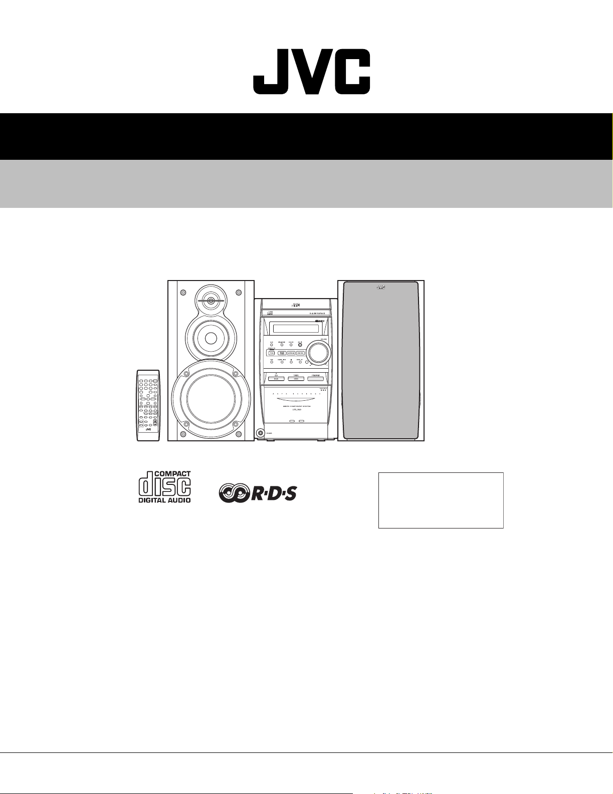
UX-J60
SERVICE MANUAL
MICRO COMPONENT SYSTEM
UX-J60
RM-SUXJ60R REMOTE CONTROL
SP-UXJ60
SP-UXJ60CA-UXJ60
Area Suffix
B -------------------------- U.K.
E ------- Continental Europe
EN --------- Northern Europe
TABLE OF CONTENTS
1 Important Safety Precautions . . . . . . . . . . . . . . . . . . . . . . . . . . . . . . . . . . . . . . . . . . . . . . . . . . . . . . . . . . . 1-2
2 Disassembly method . . . . . . . . . . . . . . . . . . . . . . . . . . . . . . . . . . . . . . . . . . . . . . . . . . . . . . . . . . . . . . . . . . 1-6
3 Adjustment. . . . . . . . . . . . . . . . . . . . . . . . . . . . . . . . . . . . . . . . . . . . . . . . . . . . . . . . . . . . . . . . . . . . . . . . . . 1-19
4 Description of major ICs. . . . . . . . . . . . . . . . . . . . . . . . . . . . . . . . . . . . . . . . . . . . . . . . . . . . . . . . . . . . . . . 1-25
COPYRIGHT © 2003 VICTOR COMPANY OF JAPAN, LTD.
No.22029
2003/03
Page 2
UX-J60
Important Safety Precautions
1.1 Safety Precautions
(1) This design of this product contains special hardware and
many circuits and components specially for safety purposes.
For continued protection, no changes should be made to the
original design unless authorized in writing by the manufacturer. Replacement parts must be identical to those
used in the original circuits. Services should be performed by qualified personnel only.
(2) Alterations of the design or circuitry of the product should
not be made. Any design alterations of the product should
not be made. Any design alterations or additions will void
the manufacturers warranty and will further relieve the
manufacture of responsibility for personal injury or property
damage resulting therefrom.
(3) Many electrical and mechanical parts in the products have
special safety-related characteristics. These characteristics are often not evident from visual inspection nor can the
protection afforded by them necessarily be obtained by using replacement components rated for higher voltage, wattage, etc. Replacement parts which have these special safety
characteristics are identified in the Parts List of Service Manual. Electrical components having such features are identified by shading on the schematics and by ( ) on the
Parts List in the Service Manual. The use of a substitute replacement which does not have the same safety characteristics as the recommended replacement parts shown in the
Parts List of Service Manual may create shock, fire, or other hazards.
(4) The leads in the products are routed and dressed with ties,
clamps, tubings, barriers and the like to be separated from
live parts, high temperature parts, moving parts and/or
sharp edges for the prevention of electric shock and fire
hazard. When service is required, the original lead routing
and dress should be observed, and it should be confirmed
that they have been returned to normal, after reassembling.
(5) Leakage shock hazard testing)
After reassembling the product, always perform an isolation
check on the exposed metal parts of the product (antenna
terminals, knobs, metal cabinet, screw heads, headphone
jack, control shafts, etc.) to be sure the product is safe to
operate without danger of electrical shock.
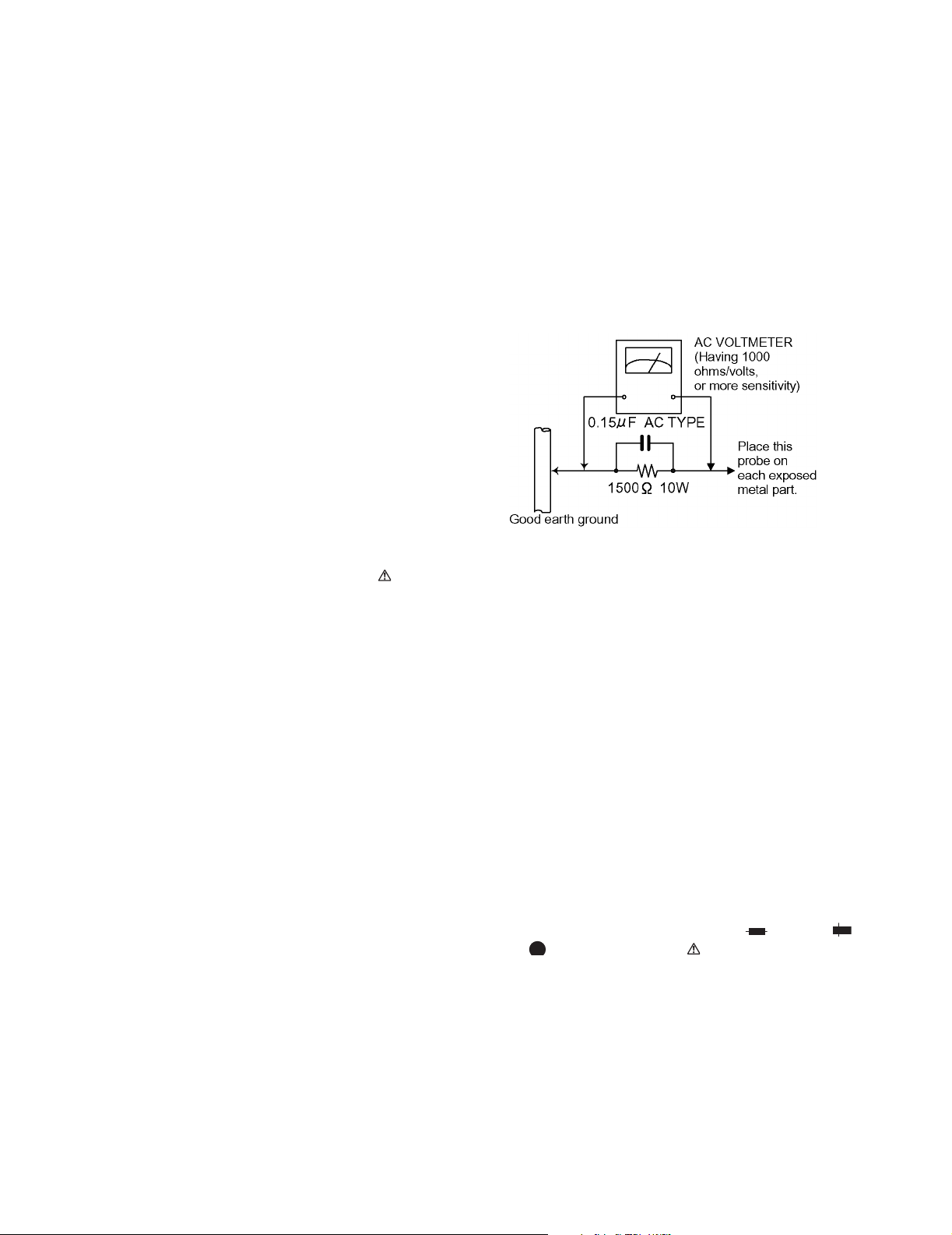
Do not use a line isolation transformer during this check.
• Plug the AC line cord directly into the AC outlet. Using a
"Leakage Current Tester", measure the leakage current
from each exposed metal parts of the cabinet, particularly any exposed metal part having a return path to the
chassis, to a known good earth ground. Any leakage current must not exceed 0.5mA AC (r.m.s.).
• Alternate check method
Plug the AC line cord directly into the AC outlet. Use an AC
voltmeter having, 1,000 ohms per volt or more sensitivity in
the following manner. Connect a 1,500 ohm 10W resistor
paralleled by a 0.15 µF AC-type capacitor between an
SECTION 1
exposed metal part and a known good earth ground.
Measure the AC voltage across the resistor with the AC
voltmeter.
Move the resistor connection to each exposed metal part,
particularly any exposed metal part having a return path to
the chassis, and measure the AC voltage across the resistor.
Now, reverse the plug in the AC outlet and repeat each
measurement. Voltage measured any must not exceed 0.75
V AC (r.m.s.). This corresponds to 0.5 mA AC (r.m.s.).
1.2 Warning
(1) This equipment has been designed and manufactured to
meet international safety standards.
(2) It is the legal responsibility of the repairer to ensure that
these safety standards are maintained.
(3) Repairs must be made in accordance with the relevant
safety standards.
(4) It is essential that safety critical components are replaced
by approved parts.
(5) If mains voltage selector is provided, check setting for local
voltage.
1.3 Caution
Burrs formed during molding may be left over on some parts
of the chassis.
Therefore, pay attention to such burrs in the case of preforming repair of this system.
1.4 Critical parts for safety
In regard with component parts appearing on the silk-screen
printed side (parts side) of the PWB diagrams, the parts that are
printed over with black such as the resistor ( ), diode ( )
and ICP ( ) or identified by the " " mark nearby are critical
for safety.
When replacing them, be sure to use the parts of the same type
and rating as specified by the manufacturer. (Except the JC version)
1-2 (No.22029)
Page 3
1.5 Safety Precautions (U.K only)
(1) This design of this product contains special hardware and many circuits and components specially for safety purposes. For con-
tinued protection, no changes should be made to the original design unless authorized in writing by the manufacturer. Replacement parts must be identical to those used in the original circuits.
(2) Any unauthorised design alterations or additions will void the manufacturer's guarantee; furthermore the manufacturer cannot
accept responsibility for personal injury or property damage resulting therefrom.
(3) Essential safety critical components are identified by ( ) on the Parts List and by shading on the schematics, and must never
be replaced by parts other than those listed in the manual. Please note however that many electrical and mechanical parts in
the product have special safety related characteristics. These characteristics are often not evident from visual inspection. Parts
other than specified by the manufacturer may not have the same safety characteristics as the recommended replacement parts
shown in the Parts List of the Service Manual and may create shock, fire, or other hazards.
(4) The leads in the products are routed and dressed with ties, clamps, tubings, barriers and the like to be separated from live parts,
high temperature parts, moving parts and/or sharp edges for the prevention of electric shock and fire hazard. When service is
required, the original lead routing and dress should be observed, and it should be confirmed that they have been returned to
normal, after re-assembling.
1.5.1 Warning
(1) Service should be performed by qualified personnel only.
(2) This equipment has been designed and manufactured to meet international safety standards.
(3) It is the legal responsibility of the repairer to ensure that these safety standards are maintained.
(4) Repairs must be made in accordance with the relevant safety standards.
(5) It is essential that safety critical components are replaced by approved parts.
(6) If mains voltage selector is provided, check setting for local voltage.
UX-J60
Burrs formed during molding may be left over on some parts of the chassis. Therefore,
pay attention to such burrs in the case of preforming repair of this system.
(No.22029)1-3
Page 4
UX-J60
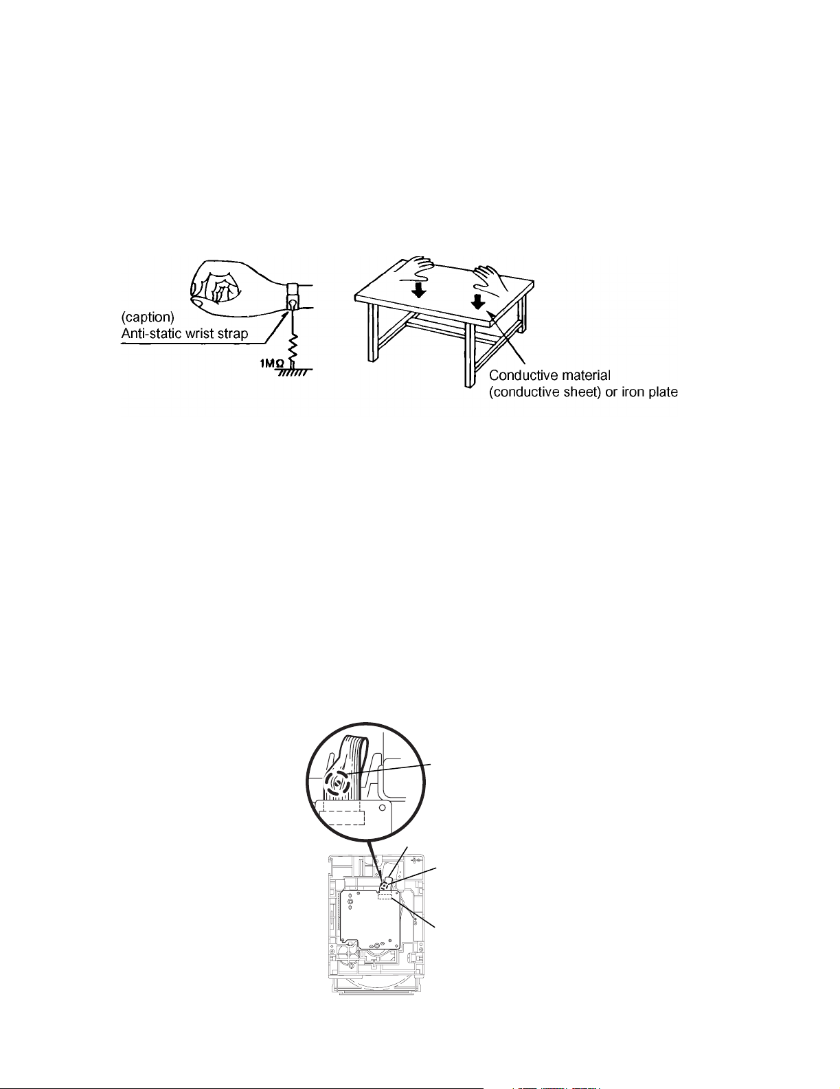
1.6 Preventing static electricity
Electrostatic discharge (ESD), which occurs when static electricity stored in the body, fabric, etc. is discharged,
can destroy the laser diode in the traverse unit (optical pickup). Take care to prevent this when performing repairs.
1.6.1 Grounding to prevent damage by static electricity
Static electricity in the work area can destroy the optical pickup (laser diode) in devices such as CD players.
Be careful to use proper grounding in the area where repairs are being performed.
(1) Ground the workbench
Ground the workbench by laying conductive material (such as a conductive sheet) or an iron plate over it before placing the
traverse unit (optical pickup) on it.
(2) Ground yourself
Use an anti-static wrist strap to release any static electricity built up in your body.
(3) Handling the optical pickup
• In order to maintain quality during transport and before installation, both sides of the laser diode on the replacement optical
pickup are shorted. After replacement, return the shorted parts to their original condition.
(Refer to the text.)
• Do not use a tester to check the condition of the laser diode in the optical pickup. The tester's internal power source can easily
destroy the laser diode.
1.7 Handling the traverse unit (optical pickup)
(1) Do not subject the traverse unit (optical pickup) to strong shocks, as it is a sensitive, complex unit.
(2) Cut off the shorted part of the flexible cable using nippers, etc. after replacing the optical pickup. For specific details, refer to the replace-
ment procedure in the text. Remove the anti-static pin when replacing the traverse unit. Be careful not to take too long a time
when attaching it to the connector.
(3) Handle the flexible cable carefully as it may break when subjected to strong force.
(4) I t is not possible to adjust the semi-fixed resistor that adjusts the laser power. Do not turn it.
1.8 Attention when traverse unit is decomposed
*Please refer to "Disassembly method" in the text for the CD pickup unit.
• Apply solder to the short land sections before the flexible wire is disconnected from the connector CN101 on the CD servo board.
(If the flexible wire is disconnected without applying solder, the CD pickup may be destroyed by static electricity.)
• In the assembly, be sure to remove solder from the short land sections after connecting the flexible wire.
Shorting round
1-4 (No.22029)
Flexible wire
Shorting round
CN601 on
mechanism
board
Page 5
1.9 Important for laser products
(1) CLASS 1 LASER PRODUCT
(2) DANGER : Invisible laser radiation when open and inter
lock failed or defeated. Avoid direct exposure to beam.
(3) CAUTION : There are no serviceable parts inside the
Laser Unit. Do not disassemble the Laser Unit. Replace the
complete Laser Unit if it malfunctions.
(4) CAUTION : The compact disc player uses invisible laser
radiation and is equipped with safety switches which
prevent emission of radiation when the drawer is open and
the safety interlocks have failed or are de feated.
It is dangerous to defeat the safety switches.
UX-J60
(5) CAUTION : If safety switches malfunction, the laser is able
to function.
(6) CAUTION : Use of controls, adjustments or performance of
procedures other than those specified herein may result in
hazardous radiation exposure.
CAUTION
Please use enough caution not to see the beam directly
or touch it in case of anadjustment or operation check.
VARNING
Osynlig laserstrålning är denna del är öppnad och spårren är
urkopplad. Betrakta ej strålen.
VARO
Avattaessa ja suojalukitus ohitettaessa olet alttiina näkymättömälle lasersäteilylle. Älä katso säteeseen.
REPRODUCTION AND POSITION OF LABELS
ADVARSEL
Usynlig laserstråling ved åbning, når sikkerhedsafbrydere er
ude af funktion. Undgå udsasttelse for stråling.
ADVARSEL
Usynlig laserstråling ved åpning, når sikkerhetsbryteren er avslott. unngå utsettelse for stråling.
Caution label
(No.22029)1-5
Page 6
UX-J60
r
A
2.1 Main body
2.1.1 Removing the metal cover
(See Fig.1~3)
(1) Remove the six screws A on the back of the main body.
(2) Remove the two screws B on each side and remove the
metal cover in the direction of the arrow.
SECTION 2
Disassembly method
A
Metal cove
A
B
Fig.2
Fig.1
B
Fig.3
1-6 (No.22029)
Page 7
2.1.2 Removing the rear cover
r
(See Fig.4)
(1) Remove the two screws C attaching the rear cover.
UX-J60
C
Rear cove
Fig.4
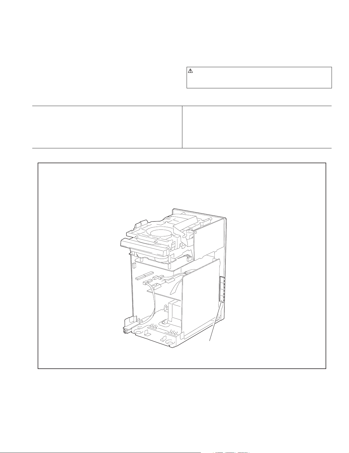
2.1.3 Removing the rear panel / fan assembly
(See Fig.5, 6)
• Prior to performing the following procedure, remove the metal
cover and the rear cover.
(1) Remove the eleven screws D attaching the rear panel. Re-
lease the two joints a on the rear side and the two joints
b on each side.
(2) Remove the two screws E attaching the fan bracket and
release the two joints c on the rear panel, and remove.
(3) Disconnect the wire from the connector CN916 on the main
board.
DD
a
Rear panel
EE
cc
Fan assembly
D
Main board
CN916
Fig.6
D
b
Fig.5
D
b
(No.22029)1-7
Page 8
UX-J60
2.1.4 Removing the tuner board
(See Fig.7)
• Prior to performing the following procedure, remove the metal
cover.
(1) Disconnect the card wire from the connector CN1 on the
tuner board.
(2) Remove the two screws F on the rear side and the screw
G in the side.
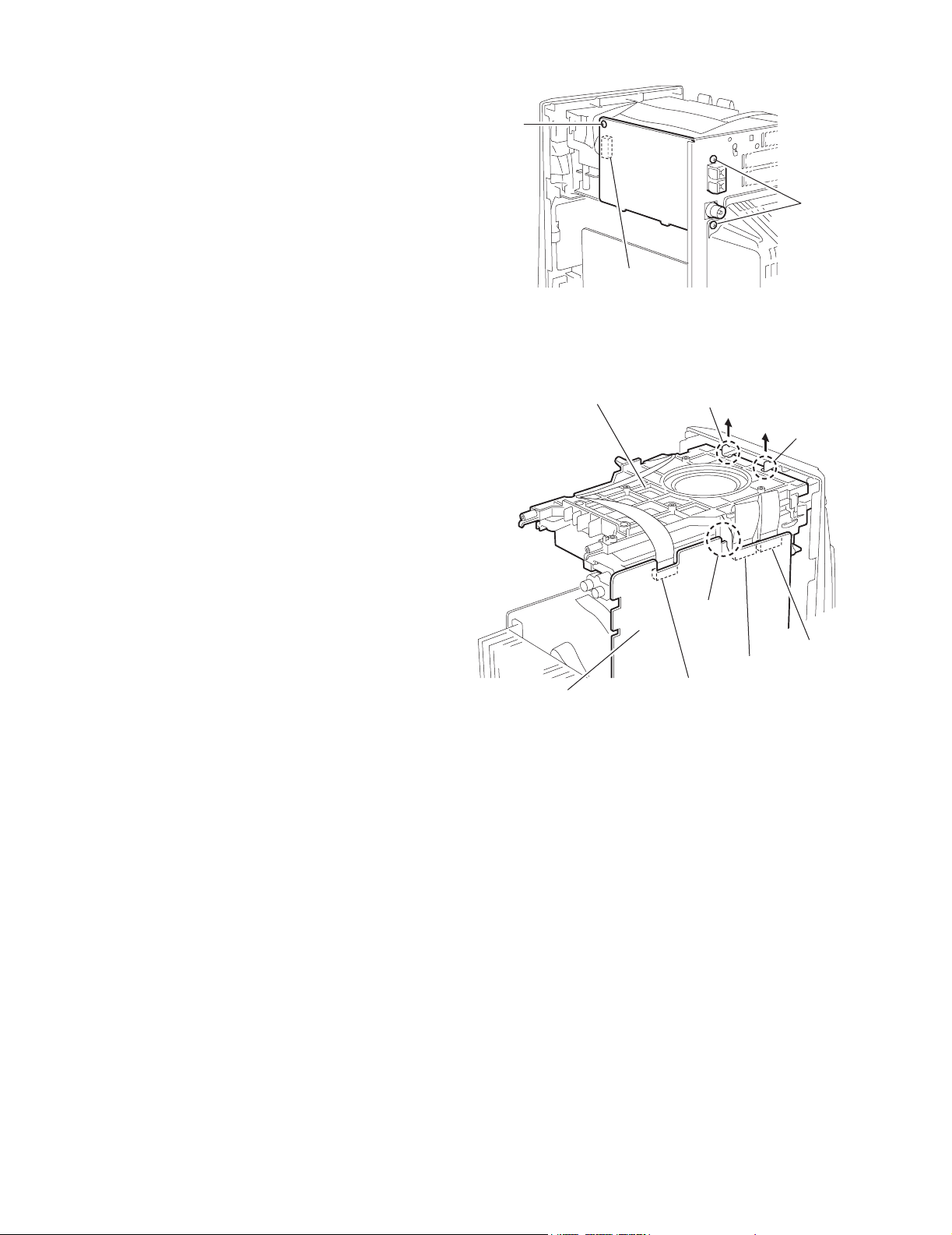
2.1.5 Removing the CD-R/RW mechanism assembly
(See Fig.8)
• Prior to performing the following procedure, remove the metal
cover, the rear cover, the rear panel and the tuner board.
(1) Disconnect the card wire from the connector CN903,
CN902 and CN904 on the main board.
(2) Pull the joint d in the direction of the arrow and remove the
CD-R/RW mechanism assembly backward while releasing
the joint e .
G
Tuner board
CN1
Fig.7
CD-R/RW mechanism assembly
F
d
d
Main board
e
CN903
CN904
CN902
Fig.8
1-8 (No.22029)
Page 9
UX-J60
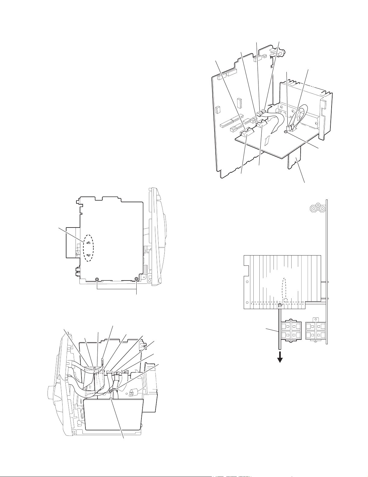
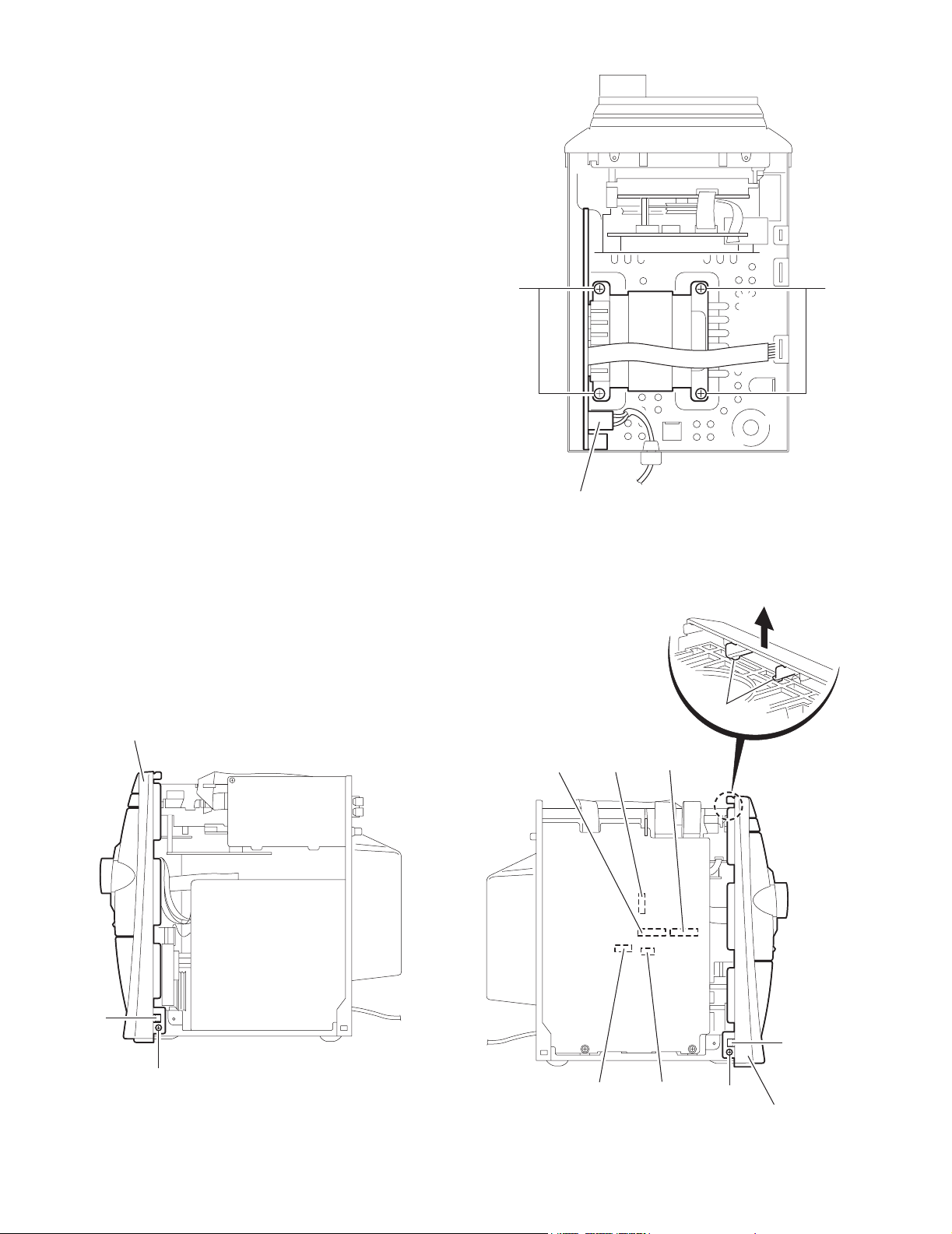
2.1.6 Removing the main board / the heat sink board / the
speaker jack board
(See Fig.9~12)
• Prior to performing the following procedure, remove the metal
cover, the rear cover, the rear panel, the tuner board and the
CD-R/RW mechanism assembly.
(1) Remove the two screws H attaching the main board.
(2) Disconnect the card wire from the connector CN900,
CN901, CN930, CN931 and CN932, and disconnect the
flat wire from the connector CN913, CN917 and CN918 on
the main board.
(3) Remove the band and disconnect the flat wire from the
connector CN951 on the power transformer assembly, and
then remove the main board / the heat sink board / the
speaker jack board from the body.
(4) Release the two joints f of the main board and disconnect
the connector CN944 and CN945 of the heat sink board
from the connector CN912 and CN911 of the main board
respectively, and disconnect the flat wire from the connector CN914 and CN915, and remove.
(5) Remove the screw I attaching the speaker jack board and
disconnect the flat wire from the connector CN946 and
CN947 on the heat sink board, and then remove the speaker jack board.
CN912
CN911
CN944
CN915
CN945
Main board
CN914
Heat sink board
CN946
Speaker jack board
Fig.11
CN947
I
f
CN930
CN913
CN931
Fig.9
Main board
CN932
CN901
H
CN900
CN917
CN918
Band
Speaker jack board
Fig.12
Power transformer assembly
CN951
Fig.10
(No.22029)1-9
Page 10
UX-J60
2.1.7 Removing the power transformer assembly
(See Fig.13)
• Prior to performing the following procedure, remove the metal
cover, the rear cover, the rear panel, the CD-R/RW mechanism assembly and the main board.
(1) Disconnect the power cord from the connector J1000 on
the power transformer assembly.
(2) Remove the four screws J .
JJ
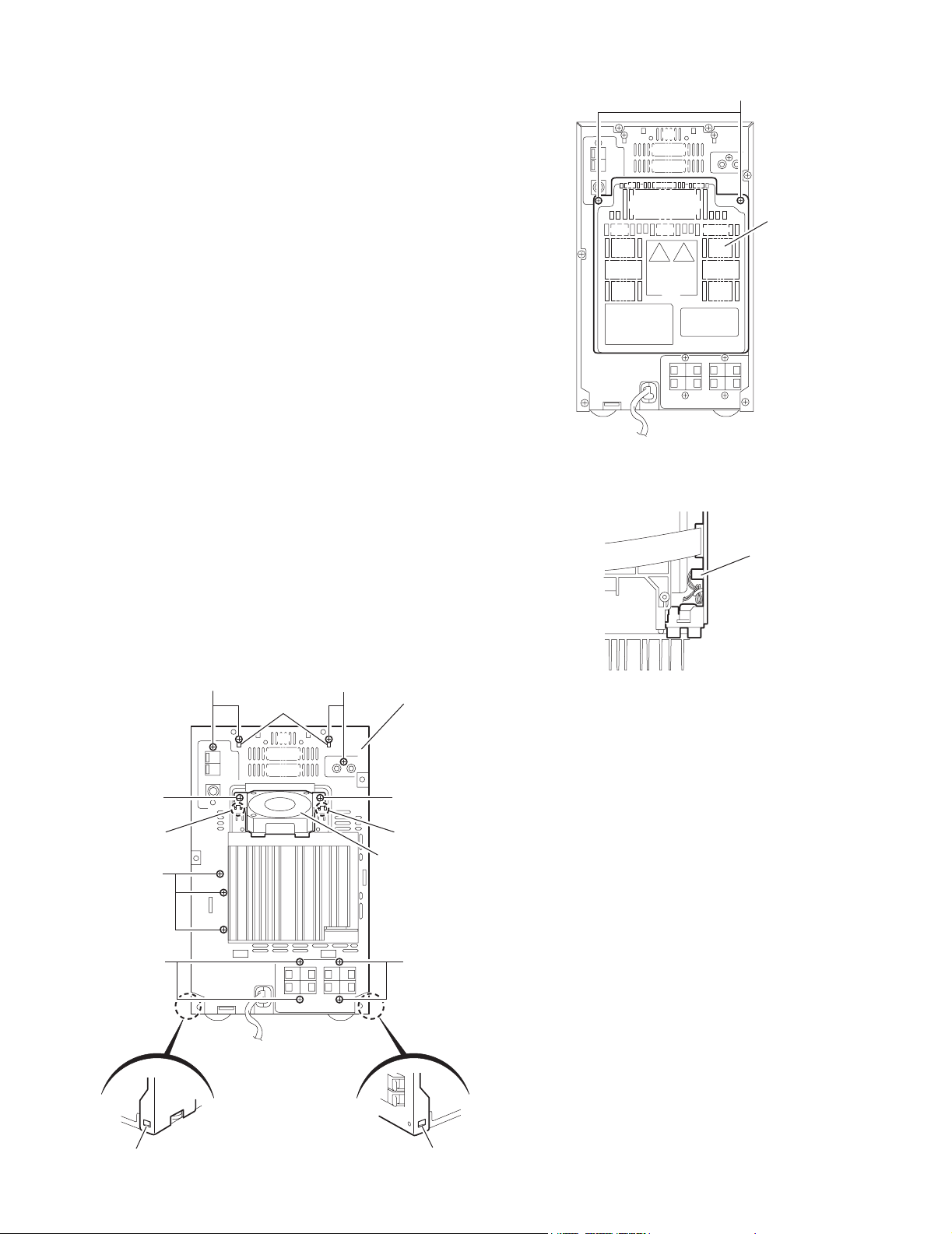
2.1.8 Removing the front panel assembly
(See Fig.14,15)
• Prior to performing the following procedure, remove the metal
cover.
(1) Remove the two screws K on each side. Release the two
joints g on the both sides and lift the front panel assembly
to release the joint h .
(2) Disconnect the card wire from the connector CN900,
CN901, CN930, CN931 and CN932 on the main board.
Front panel assembly
Powe transformer assembly
J1000
Fig.13
h
Main board
CN932CN931 CN930
g
1-10 (No.22029)
K
Fig.14
CN900
CN901
Fig.15
g
K
Front panel assembly
Page 11
2.1.9 Removing the phones board
(See Fig.16)
• Prior to performing procedure, remove the metal cover and the
front panel assembly.
(1) Disconnect the flat wire from the connector CN913 on the
main board.
UX-J60
Mian board
CN913
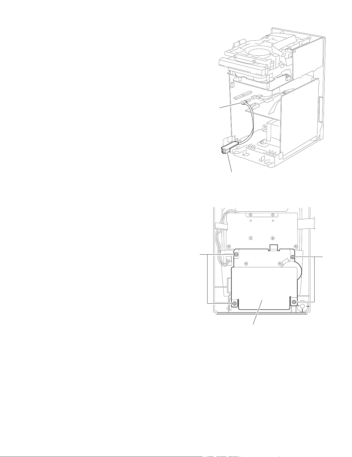
2.1.10 Removing the cassette mechanism assembly
(See Fig.17)
• Prior to performing the following procedure, remove the metal
cover and the front panel assembly.
(1) Remove the four screws L attaching the cassette mecha-
nism assembly.
Phones board
Fig.16
L
Cassette mechanism assembly
Fig.17
L
(No.22029)1-11
Page 12
UX-J60
2.1.11 Removing the switch board
(See Fig.18,19)
• Prior to performing the following procedure, remove the metal
cover and the front panel assembly.
(1) Remove the four screws M attaching the switch board.
(2) Move the switch board in the direction of the arrow to dis-
connect the wire from the connector CN762 and the card
wire from the connector CN761.
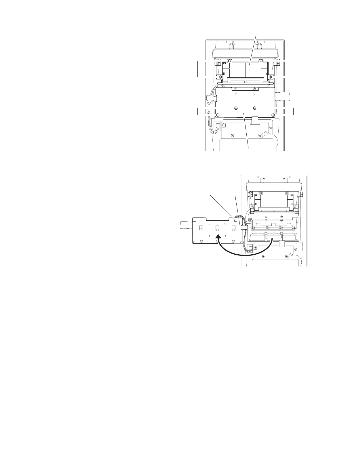
2.1.12 Remove the LCD board assembly
(See Fig.18)
• Prior to performing the following procedure, remove the metal
cover and the front panel assembly.
(1) Remove the four screws N attaching the LCD board as-
sembly.
M
Switch board
CN762 CN761
LCD board assembly
NN
M
Switch board
Fig.18
Fig.19
1-12 (No.22029)
Page 13
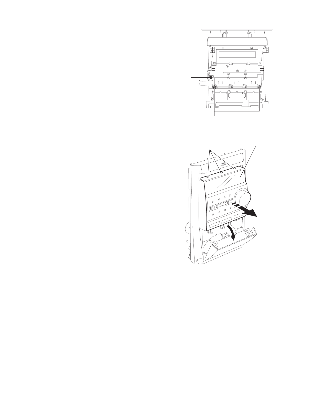
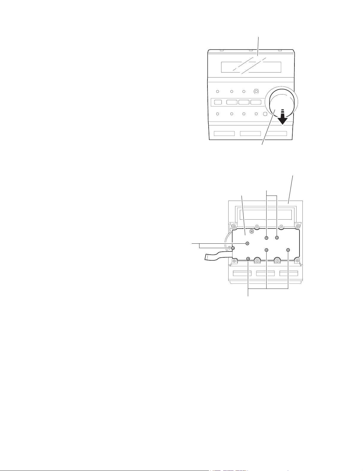
2.1.13 Removing the control panel assembly
(See Fig.20,21)
• Prior to performing the following procedure, remove the metal
cover, the front assembly, the switch board and the LCD board
assembly.
(1) Remove the three screws O attaching the control panel as-
sembly.
(2) Release the three joints i and open the cassette door
while pressing the cassette door, and then remove the control panel assembly in the direction of the arrow.
UX-J60
O
O
Fig.20
i
Cotrol panel assembly
Fig.21
(No.22029)1-13
Page 14
UX-J60
2.1.14 Remiving the control board
(See Fig.22,23)
• Prior to performing the following procedure, remove the metal
cover, the front panel assembly, the switch board, the LCD
board assembly and the control panel assembly.
(1) Pull out the volume knob.
(2) Remove the seven screws P attaching the control board.
Control panel assembly
Volume knob
Fig.22
Control panel assembly
P
Control board
P
P
Fig.23
1-14 (No.22029)
Page 15

2.2 Cassette mechanism assembly
2.2.1 Removing the Play/Record & Clear head
(See Fig.1~3)
(1) While moving the trigger arm on the right side of the head
mount in the direction of the arrow, turn the flywheel R
counterclockwise until the head mount comes ahead and
clicks.
(2) The head turns counterclockwise as you turn the flywheel
R counterclockwise (See Fig.2 and 3).
(3) Disconnect the flexible wire from connector CN31 on the
head amplifier & mechanism control board.
(4) Remove the spring from the back of the head.
(5) Loosen the azimuth screw for reversing attaching the head.
(6) Remove the head on the front side of the head mount.
Cassette mechanism assembly
Fig.1
Head
UX-J60
Fly wheelR
Trigger armHead mount
Flexible wire
Fly wheel R
Fig.2
Azimuth screw
Head
for reversing
Spring
CN31
Head amplifer & mecha control board
Fig.3
(No.22029)1-15
Page 16

UX-J60
2.2.2 Removing the head amplifier & mechanism control board
(See Fig.4)
(1) Turn over the cassette mechanism assembly and remove
the three screws A attaching the head amplifier & mechanism control board.
(2) Disconnect the flexible wire from connector CN31 on the
head amplifier & mechanism control board.
(3) Disconnect connector CN32 of the head amplifier & mech-
anism control board from connector CN1 on the reel pulse
board.REFERENCE: If necessary, unsolder the 4-pin wire
soldered to the main motor.
2.2.3 Removing the main motor
(See Fig.4~7)
(1) Remove the two screws B .
(2) Half raise the motor and remove the capstan belt from the
motor pulley.
ATTENTION:
Be careful to keep the capstan belt from grease. When reassembling, refer to Fig.6 and 7 for attaching the capstan belt.
Head amplifier & mecha control board
Main motor assembly
Capstan belt
Fig.5
Main motor assembly
CN31
Flexible wire
A
AA
Fig.4
CN32
4pin wire
B
Main motor assembly
Motor pulley
Capstan belt
Fig.6
Main motor assembly
Fly wheel
1-16 (No.22029)
Capstan belt
Motor pulley
Fig.7
Page 17

2.2.4 Removing the flywheel
(See Fig.8, 9)
• Prior to performing the following procedure, remove the head
amplifier & mechanism control board and the main motor assembly.
(1) From the front side of the cassette mechanism, remove the
slit washers attaching the capstan shaft L and R. Pull out
the flywheels backward.
UX-J60
Fly wheel R Fly wheel L
Fig.8
Fly wheel R
Capstan shaft R Capstan shaft L
Slit washer
Fig.9
2.2.5 Removing the reel pulse board and solenoid
(See Fig.10)
• Prior to performing the following procedure, remove the head amplifier & mechanism control board.
(1) Remove the screw C.
(2) Release the tab a, b, c, d and e retaining the reel pulse board.
(3) Release the tab f and g attaching the solenoid on the reel pulse board.
(4) The reel pulse board and the solenoid come off.
d
Reel pulse board
Solenoid
a
bc
Fly wheel L
g
f
C
e
Fig.10
(No.22029)1-17
Page 18

UX-J60
r
r
2.2.6 Reattaching the Play/ Record & Clear head
(See Fig.11~13)
(1) Reattaching the head mount assembly.
a) Change front of the direction cover of the head
mount assembly to the left (Turn the head forward).
b) Fit the bosses O', P', Q', U' and V' on the head mount
assembly to the holes P and V, the slots O, U and Q
of the mechanism sub assembly (See Fig.11 to 13).
CAUTION:
To remove the head mount assembly, turn the direction
cover to the left to disengage the gear. If the gear can not
be disengaged easily, push up the boss Q' slightly and
raise the rear side of the head mounts slightly to return
the direction lever to the reversing side.
(2) Tighten the azimuth screw for reversing.
(3) Reattach the spring from the back of the Play/ Record &
Clear head.
(4) Connect the flexible wire to connector CN31 on the head
amplifier & mechanism control board.
U' Q'
Head mount assembly
Head mount assembly
O'
Fig.11
P'
P'
V'
V'
Direction cove
Spring
Flexible wire
V
O
P
Q
Head
Direction cove
U
Fig.12
Azimuth screw for reversing
Head mount
1-18 (No.22029)
CN31
Fig.13
Head amplifier &
mechanism control board
Page 19

3.1 Adjustment method
V
V
a
)
e
t
F
r
8
t
e
UX-J60
SECTION 3
Adjustment
Measurement Instruments Required for
Adjustment
1. Low frequency oscillator
This oscillator should have a capacity to output
0dBs to 600 at an oscillation frequency of
50Hz-20kHz.
2. Attenuator impedance : 600
3. Electronic voltmeter
4. Distortion meter
5. Frequency counter
6. Wow & flutter meter
7. Test tape
VT703L : Head azimuth
VT712 : Tape speed and running unevenness
(3kHz)
VT724 : Reference level (1kHz)
8. Blank tape
TYPE : AC-225
TYPE : AC-514
9. Torque gauge : For play and back tension
FWD(TW2111A), REV(TW2121a) and
FF/REW(TW2231A)
10. Test disc: CTS-1000
Measurement conditions
Power supply voltage
AC 230V ~ , 50Hz
Reference output : Speaker : 0.775V/4
: Headphone : 0.077V/32
Reference frequency and
input level ------------------------------ 1kHz, AUX : -8dBs
Measurement output terminal ------- at Speaker J3002
Load resistance --------------------------- 4
Radio Input signal
AM frequency --------------------------------------- 400Hz
AM modulation ---------------------------------------- 30%
FM frequency --------------------------------------- 400Hz
FM frequency deviation ------------------------ 22.5kHz
Tuner section
FM tuning range: 87.5MHz~108.00MHz
AM tuning range: 522kHz~1,629kHz
Voltage applied to tuner +B : DC5.7
VT : DC 12
Reference measurement
output 26.1mV(0.28V)/3
Input positions AM : Standard loop antenn
FM : TP1 (hot) and TP2 (GND
Standard measurement position of volume
Function switch to Tap
Beat cut switch to Cu
Super Bass/Active hyper Bass to OF
Bass Treble to Cente
Adjustment of main volume to reference output
VOL : 2
Precautions for measurement
1. Apply 30pF and 33k to the IF sweeper output
side and 0.082 F and 100k in series to the
sweeper input side.
2. The IF sweeper output level should be made as
low as possible within the adjustable range.
3. Since the IF sweeper is a fixed device, there is no
need to adjust this sweeper.
4. Since a ceramic oscillator is used, there is no need
to perform any MIX adjustment.
5. Since a fixed coil is used, there is no need to adjus
the FM tracking.
6. The input and output earth systems are separated.
In case of simultaneously measuring the voltage in
both of the input and output systems with an
electronic voltmeter for two channels, therefore, the
earth should be connected particularly carefully.
7. In the case of BTL connection amp., the minus
terminal of speaker is not for earthing. Therefore, b
sure not to connect any other earth terminal to this
terminal. This system is of an BTL system.
8. For connecting a dummy resistor when measuring
the output, use the wire with a greater code size.
9. Whenever any mixed tape is used, use the band
pass filter (DV-12).
(No.22029)1-19
Page 20

UX-J60
3.2 Cassette mechanism adjustment
Head azinuth
adjustment screw
(Forward side)
Mecha control board
Head azinuth
adjustment screw
(Reverse side)
SW1
SW2
Head azinuth
adjustment screw
(Forward side)
Head azinuth
adjustment screw
(Reverse side)
CN31
R/P head, Erase head
P1
D1
VR37
R371
CN1
FW100
SW5
Motor speed
VR37
BIAS adjust
VR31
C308
R327
VR31
R313
Q302
R315
C316
C319
C221
R314
L301
C121
C314
R104
Q305
C313
D340
C310
R304
R310
C107
L303
R102
R121
R221
R303
R335
R353
R339
R108
C113
R302
Q343
C301
C103
C207
R301
Q342
C105
C205
C304
R208
C106
R101
C104
R306
R106
Q344
CN34
C306
R344
R105
C102
R205
R110
Q345
R345
C307
R336
C340
C206
R346
R206
W1
R107
Q346
R305
C110
R210
C300
C341
R109
R372
Q372
C371
CN33
IC32
R116
C109
CN31
Q371
C101
C374
R376
R216
Q375
C376
R204
R201
C202
C204
C201
CN32
C203
R202
C210
R340
C331
R342
R347
Q347
SW6
R343
R341
IC33
IC1
D375
Q376
R338
R375
R337
C213
C342
C209
W1
R207
1-20 (No.22029)
Page 21

3.2.1 Mechanism section
t
W
t
t
UX-J60
Item Condition Measurement method Ref.value
Head
azimuth
Test tape
: VT703L (8kHz)
Output terminal
: Speaker out
1.Playback the test tape VT703L (8kHz).
2.Adjust to maximum output level by azimuth
adjustment screw for forward side and reverse
side.
Maximum
output
3.This adjustment is adjust by adjustment screw
of forward side and adjustment screw of reverse
side.
Tape speed
Test tap
: VT712 (3kHz)
Output terminal
Playback the test tape VT712 (3kHz) at end of
forward side,adjust to 2,940~3,90Hz indication
of frequency counter by VR37.
2,940 ~
3,090Hz
: Speaker out or
Headphone out
Adjustmen
position
Only adjus
at changed
head
VR37
Item Condition Measurement method Ref.value
Tape speed
diviation at
FWD/REV
Test tape
: VT712 (3kHz)
Output terminal
Playback the test tape VT712 (3kHz) at end
of forward and reverse, tape speed deviation
should be less than 6.0Hz.
Leass than
6.0Hz
: Speaker out or
Headphone out
ow & Flutter Playback the test tape VT712 (3kHz) at
Test tape
: VT712 (3kHz)
Output terminal
start of forward and reverse,Wow & Flutter
are should be less than 0.25%(WRMS).
Less than
0.25%
(WRMS)
: Speaker out or
Headphone out
Adjustmen
position
VR31
(No.22029)1-21
Page 22

UX-J60
R
t
3.2.2 Electrical adjustment
Item Condition Measurement method Ref.value
Recording
BIAS
adjustment
Forward or Reverse
Test tape
:AC-514 TYPE
:AC-225 TYPE
Output terminal
Recording head
1.Set the test tape(AC-514 TYPE and
AC-225 TYPE ), then make REC/PAUSE
condition.
2.Connect 100 to recording head by series,
then connect to VTVM for measurement the
current.
AC-225
:4.20 A
AC-514
:4.0 A
3.After setting, start the recording by release
the PAUSE, in this time bias current adjust
to next fig. by VR31 for Lch and VR32 for
Rch.
4.0 A (TYPE ) and 4.20 A (TYPE ).
R/P
playback
frequency
response
Reference frequency
: 1kHz / 10kHz
(Reference: -20dB)
Test tape
: AC-514 TYPE
Input terminal
: OSC IN
1.Set the test tape (AC-514 TYPE ), then
make REC/PAUSE condition.
2.Release the PAUSE, then start recording
the 1kHz and 10kHz of reference frequency
from oscillator.
3.Playback the recorded position, 1kHz and
10kHz output deviation should -1dB 2dB
Output
deviation
1kHz/10kHz
:-1dB 2dB
to readjust by VR31 for Lch and VR32 for
Rch.
Adjustment
position
VR31
VR31
3.2.3 Electrical response confirmation
Item Condition Measurement method Ref.value
ecording
bias
current
Forward or Reverse
Test tape
: TYPE (AC-514)
Measurement
terminal
: BIAS test point on
printed circuit board
Erase
current
(reference
value)
Forward or Reverse
Rec condition
Test tape
: AC-514 TYPE
: AC-225 TYPE
Measurement
terminal
: Both side of Erase
head
1.Change BIAS1 and 2, confirm the frequency
should be change.
2.Set the test tape (AC-514 TYPE ), then
make REC/PAUSE condition.
3.Confirm the frequency should 100Hz 6kHz
at BIAS test point on printed circuit board.
1.Set the test tape (AC-514 TYPE and
AC-225 TYPE ), then make REC/PAUSE
condition.
2.Release the PAUSE to REC condition,
connect 1W to ERASE head by series, then
confirm the erase current at both side of
erase head.
Adjustmen
position
100 kHz
6 kHz
TYPE
: 120 mA
TYPE
: 75 mA
1-22 (No.22029)
Page 23

3.3 Flow of functional operation until TOC read (CD)
Power ON
Power Key
Slider turns REST
SW ON.
Automatic tuning
of TE offset
UX-J60
Check Point
Check that the voltage at the pin 5
of CN801 is 0V?
VREF
Tracking error waveform at TOC reading
pin 20 of
IC601(TE)
Approx
1.7V
Tracking
servo
Disc start
to rotate
off
Automatic measurement
of TE amplitude and
automatic tuning of
TE balance
Approx.1sec
Tracking
servo ON
Disc to be
braked to stop
TOC reading
finishes
500mv/div
2ms/div
Fig.1
Laser ON
Detection of disc
Automatic tuning of
Focus offset
Automatic measurement of
Focus S-curve amplitude
Disc is rotated
Focus servo ON
(Tracking servo ON)
Automatic measurement of
Tracking error amplitude
Automatic tuning of
Tracking error balance
Check that the voltage at the
pin2 of IC601 is 4.4V?
Confirm that the Focus error
S-cuve, ie at the pin23 of
IC601 is approx.2Vp-p
Confirm that the siganl from
pin 5,6 of IC801 is a 2V
accelerated pulse with approx.
700ms.
Confirm the waveform of
the Tracking error signal
at the pin20 of IC601
(See fig-1)
Automatic tuning of
Focus error balance
Automatic tuning of
Focus error gain
Automatic tuning of
Tracking error gain
TOC reading
Play a disc
Confirm the eye-pattern
at the lead of TP1
(No.22029)1-23
Page 24

UX-J60
3.4 Maintenance of laser pickup (CD)
(1) Cleaning the pick up lens
Before you replace the pick up, please try to clean the lens
with a alcohol soaked cotton swab.
(2) Life of the laser diode
When the life of the laser diode has expired, the following
symptoms will appear.
• The level of RF output (EFM output: ampli tude of eye
pattern) will be low.
Is the level of
RFOUT under
1.25V 0.22Vp-p?
NO
Replace it.
YES
O.K
(3) Semi-fixed resistor on the APC PC board
The semi-fixed resistor on the APC printed circuit board
which is attached to the pickup is used to adjust the laser
power.Since this adjustment should be performed to match
the characteristics of the whole optical block, do not touch
the semi-fixed resistor.
If the laser power is lower than the specified value,the laser
diode is almost worn out, and the laser pickup should be replaced. If the semi-fixed resistor is adjusted while the pickup is functioning normally, the laser pickup may be
damaged due to excessive current.
3.5 Replacement of laser pickup (CD)
Turn off the power switch and, disconnect the
power cord from the ac outlet.
Replace the pickup with a normal one.(Refer
to "Pickup Removal" on the previous page)
Plug the power cord in, and turn the power on.
At this time, check that the laser emits for
about 3seconds and the objective lens moves
up and down.
Note: Do not observe the laser beam directly.
Play a disc.
Check the eye-pattern at TP1.
Finish.
1-24 (No.22029)
Page 25

Description of major ICs
4.1 AN22000A-W (IC601) : RF & SERVO AMP
• Terminal layout
• Block diagram
RFOUT
RF_EQ
32
31
30
29
27
28
AMP
AMP
AMP
AMP17GCA BCA
+
-
ACBDPDF
323130292827262524232221201918
123456789
LD
PD
PDE
TBAL
RFN
VCC
RFIN
CAGC
RFOUT
624754 8
RFIN
AGC
NRFDET
GCA BCA
GCA BCA
GCA BCA
FBAL
GCTRL
FEOUT
FEN
10111213141516
ARF
CEA
CBDO
3TOUT
11 12
BDO
TEN
TEOUT
BDO
COFTR
SUBT
SUBT
TEBPF
OFTR
VDET
VREF
17
GND
RFDET
13 14
OFTR
3TENV
VDET
SECTION 4
9
10
15
22
-
+
-
+
-
+
23
21
20
19
18
2
LD
• Pin function
Pin
Symbol I/O Function
No.
1 PD I APC Amp. input terminal
2 LD O APC Amp. output terminal
3 VCC - Power supply terminal
4 RFN I RF adder Amp. inverting input terminal
5 RFOUT O RF adder Amp. output terminal
6 RFIN I AGC input terminal
7 CAGC I Input terminal for AGC loop filter capacitor
8 ARF O AGC output terminal
9 CEA I Capacitor connecting terminal
for HPF-Amp.
10 3TOUT O 3 TENV output terminal
11 CBDO I Capacitor connecting terminal for envelope
detection on the darkness side
12 BDO O BDO output terminal
13 COFTR I Capacitor connecting terminal for envelope
detection on the light side
14 OFTR O OFTR output terminal
15 NRFDET O NRFDET output terminal
16 GND - Ground
17 VREF O VREF output terminal
18 VDET O VDET output terminal
19 TEBPF I VDET output terminal
20 TEOUT O TE Amp. output terminal
21 TEN I TE Amp. inverting input terminal
22 FEN I FE Amp. inverting input terminal
23 FEOUT O FE Amp. output terminal
24 GCTL O GCTL & APC terminal
25 FBAL O FBAL control terminal
26 TBAL O TBAL control terminal
27 E I Tracking signal input terminal 1
28 F I Tracking signal input terminal 2
29 D I Focus signal input terminal 4
30 B I Focus signal input terminal 3
31 C I Focus signal input terminal 2
32 A I Focus signal input terminal 1
UX-J60
GCTL26TBAL
25 16 3
FBAL
PD
1
(No.22029)1-25
Page 26

UX-J60
4.2 HA12238F (IC32) : R/P Equalizer
• Pin layout
PB-NF1(L)
TEST 2
RIP
PBIN(l)
REC Return
GND
PBIN(R)
NC
TEST 3
PB-NF1(R)
31
32
33
34
35
36
37
38
39
40
PB-NF2(L)
PB-EQ(L)
30
29
+
Return SW
Return SW
+
-
EQ OUT(L)
TAI(L)
28
27
MUTE
MUTE
NC
PB OUT(L)
26
25
REC IN(L)
ALC(L)
24
23
NC
22
EQ
EQ
REC OUT(L)
21
ALC
TEST
20
(Open for nomal use)
19
Iraf
18
GND
ALC DET
17
16
Vcc
REC MUTE OFF/ON
15
MUTO ON/OFF
14
REC RETURN ON/OFF
13
TEST 4
12
ALC ON/OFF
11
1
2
PB-EQ(R)
PB-NF2(R)
3
4
TAI(R)
EQOUT(R)
5
6
NC
PB OUT(R)
7
8
ARC(R)
REC IN(R)
9
10
NC
REC OUT(R)
1-26 (No.22029)
Page 27

• Pin function
Pin No. Symbol Function
1 PB-NF2(R) PB EQ feed back
2 PB-EQ(R) NAB output
3 EQOUT(R) EQ output
4 TAI(R) Tape input
5 PBOUT(R) PB output
6 NC NC pin
7 REC IN(R) REC-EQ input
8 ALC(R) ALC(R) signal out put
9 NC NC pin
10 REC OUT(R) REC output
11 ALC ON/OFF Mode control input
12 TEST4 TEST pin
13 REC Return ON/OFF Mode control input
14 MUTE ON/OFF Mode control input
15 REC Return ON/OFF Mode control input
16 Vcc Vcc Pin
17 ALC DET ALC detection signal out put
18 GND GND pin
19 I REF Equalizer reference current input
20 Test mode Test modepin
21 REC OUT(L) REC output
22 NC NC pin
23 ALC(L) ALC(L) signal out put
24 REC IN(L) REC-EQ input
25 NC NC pin
26 PBOUT(L) PB output
27 TAI(L) Tape input
28 EQOUT(L) EQ output
29 PB-EQ(L) NAB output
30 PB-NF2(L) PB EQ feed back
31 PB-NF1(L) PB EQ feed back
32 TEST2 TEST pin
33 RIP Ripple fillter
34 PBIN(L) PB input
35 REC-RETURN REC Return
36 GND GND pin
37 PBIN(R) PB input
38 NC NC pin
39 TEST3 TEST pin
40 PB-NF1(R) PB EQ feed back
UX-J60
(No.22029)1-27
Page 28

UX-J60
4.3 GP1UM261XK (IC750) : Receiver
• Pin layout
Vout
• Block diagram
GND
Vcc
4.4 HA17758A (IC902,IC944) : Dual Operational Amp
• Pin layout
8
7
6
5
VCC
Vout2
Vin(-)2
Vin(+)2
Vout1
Vin(-)1
Vin(+)1
VEE
1
1
- +
2
2
+ -
3
4
B.P.F.LimiterAmp
Demodulator
Integrator
Comparator
GND Vdd Vout
1-28 (No.22029)
Page 29

4.5 KIA7810API (IC942) : Regulater
• Pin Layout
• Block Diagram
UX-J60
1
R23R17R22
INPUT
Z1
R12
R11
Q12
Q13
R18
Q2
Q18
Q11R1
R2
R3
Q17
Q1
Q3
Q4
Q19
Q6
R7
Q14
Q5
Q19
C1
Q7
Q9 Q8
Q9
Q11-1
R10
R15
Q10
Q15
R14
R16
R20
R21
Q16
3
OUTPUT
R13
R4
R5 R6 R8
2
COMMON(GND)
(No.22029)1-29
Page 30

UX-J60
4.6 KIA78R08PI (IC943) :Regulater
• Pin Layout
• Block Diagram
1 2
V1N
V1N
Control
OUTPUT ON/OFF
4
BANDGAP
REFERENCE
CONTROL
ASO
PROTECTION
OVER HEAT
PROTECTION
3
GND
VO
-
+
1-30 (No.22029)
Page 31

4.7 KIA78S06P-T (IC932) : Regulator
•Pin layout
1 2 3
• Block diagram
UX-J60
3 INPUT
Z1
Q14
Q1
R9
Q16
Q2 Q7
R11 R10
R1
Q4
Q3
Q6
Q5
R4
Q11
C1
Q10
R2
Q9
Q8
R3
4.8 LB1641 (IC802) : DC Motor driver
•Pin layout •Truth table
1
GND
OUT1
P1
VZ
IN1
IN2
VCC1
VCC2
P2
OUT2
2
3
4
5
6
7
8
9
10
Input Output Mode
IN1 IN2 OUT1 OUT2
0000 Brake
1 0 1 0 CLOCKWISE
0 1 0 1 COUNTER-CLOCKWISE
1100 Brake
Q12
R8
Q13
R7R5R6
1 OUTPUT
2 COMMON
(No.22029)1-31
Page 32

UX-J60
4.9 LA1838 (IC1): FM AM IF AMP&detector, FM MPX Decoder
• Block Diagram
30
ALC
BUFF
FM
S-METER
FM IF
1
29
AM
OSC
S-CLRVE
PM
DET
2
28
REG
AM
MIX
SD
COMP
AM/FM
IF-BUFF
3
27
FM
RF.AMP
AM IF
4
26
AGC
AM
S-METER
GND
25
24
DET
TUNING
DRIVE
5
6
STEREO
DRIVE
7
22
23
P-DET
VCC
89
VCO
384KHz
21
DECODER
ANIT-BIRDIE
STEREO
5N
SW
10
20
FF
38k
11
18
19
MUTE
FF
/
19k
2
12 13
FF
19k
17 16
/LS
14
PILOT
DET
15
• Pin Function
Pin No. Symbol I/O Function
1 FM IN I This is an input terminal of FM IF signal.
2 AM MIX O This is an out put terminal for AM mixer.
3 FM IF I Bypass of FM IF
4 AM IF I Input of AM IF Signal.
5 GND - This is the device ground terminal.
6
7
TUNED
STEREO
O When the set is tunning,this terminal becomes "L".
O Stereo indicator output. Stereo "L", Mono: "H"
8 VCC - This is the power supply terminal.
9 FM DET - FM detect transformer.
10 AM SD - This is a terminal of AM ceramic filter.
11 FM VSM O Adjust FM SD sensitivity.
12 AM VSM O Adjust AM SD sensitivity.
13 MUTE I/O When the signal of IF REQ of IC121(LC72131) appear, the signal of FM/AM IF output. //Muting
control input.
14
15
FM/AM
MONO/ST
I Change over the FM/AM input. "H" :FM, "L" : AM
O Stereo : "H", Mono: "L"
16 L OUT O Left channel signal output.
17 R OUT O Right channel signal output.
18 L IN I Input terminal of the Left channel post AMP.
19 R IN I Input terminal of the Right channel post AMP.
20 RO O Mpx Right channel signal output.
21 LO O Mpx Left channel signal output.
22 MPX IN I Mpx input terminal
23 FM OUT O FM detection output.
24 AM DET O AM detection output.
25 AM AGC I This is an AGC voltage input terminal for AM
26 AFC - This is an output terminal of voltage for FM-AFC.
27 AM RF I AM RF signal input.
28 REG O Register value between pin 26 and pin28 besides the frequency width of the input signal.
29 AM OSC - This is a terminal of AM Local oscillation circuit.
30 OSC BUFFER O AM Local oscillation Signal output.
1-32 (No.22029)
Page 33

4.10 LA6541-X (IC801) : Servo driver
• Pin layout & Block diagram
Vcc Vref Vin4 Vg4 Vo8 Vo7
24 23
22
21
11k
ohm
UX-J60
20
19
Gnd
Vcc
Vo6 Vo5 Vg3 Vin3 Cd Res
18
17 16
15
14
13
11k
ohm
- +
- +
Level
shift
Level
shift
B T L
driver
B T L
driver
11k
ohm
1
Vcc Mute Vin1 Vg1 Vo1 Vo2 Vo3 Vo4 Vg2 Vin2 Reg
2
3456
Gnd
78 9101112
• Pin function
Pin No. Symbol Description
1 Vcc Power supply (Shorted to pin 24)
2 Mute All BTL amplifier outputs ON/OFF
3 Vin1 BTL AMP 1 input pin
4 Vg1 BTL AMP 1 input pin (For gain adjustment)
5 Vo1 BTL AMP 1 input pin (Non inverting side)
6 Vo2 BTL AMP 1 input pin (Inverting side)
7 Vo3 BTL AMP 2 input pin (Inverting side)
8 Vo4 BTL AMP 2 input pin (Non inverting side)
9 Vg2 BTL AMP 2 input pin (For gain adjustment)
10 Vin2 BTL AMP 2 input pin
11 Reg Out External transistor collector (PNP) connection. 5V power supply output
12 Reg In External transistor (PNP) base connection
13 Res
Reset output
14 Cd Reset output delay time setting (Capacitor connected externally)
15 Vin3 BTL AMP 3 input pin
16 Vg3 BTL AMP 3 input pin (For gain adjustment)
17 Vo5 BTL AMP 3 output pin (Non inverting side)
18 Vo6 BTL AMP 3 output pin (Inverting side)
19 Vo7 BTL AMP 4 output pin (Inverting side)
20 Vo8 BTL AMP 4 output pin (Non inverting side)
21 Vg4 BTL AMP 4 output pin (For gain adjustment)
22 Vin4 BTL AMP 4 output pin
23 Vref Level shift circuit's reference voltage application
24 Vcc Power supply (Shorted to pin 1)
B T L
driver
B T L
driver
Level
shift
Level
shift
11k
ohm
out
RESET
Regulator
Reg
In
(No.22029)1-33
Page 34

UX-J60
4.11 LC72136N (IC2) : PLL frequency synthesizer
• Pin layout
1
XT
FM/AM
CE
DI
CLOCK
DO
FM/ST/VCO
AM/FM
SDIN
2
3
4
5
6
7
8
9
10
11
22
21
20
19
18
17
16
15
14
13
12
XT
GND
LPFOUT
LPFIN
PD
VCC
FMIN
AMIN
IFCONT
IFIN
• Block diagram
1
22
16
15
3
4
5
6
17
21
1/2
C
I/F
2B
Power
on
Reset
Data Shift Register & Latch
782
• Pin function
Pin
No.
Symbol I/O Function
1 XT I X'tal oscillator connect (75kHz)
2FM
/AM O LOW:FM mode
3 CE I When data output/input for 4pin(input)
and 6pin(output): H
4 DI I Input for receive the serial data from
controller
5 CLOCK I Sync signal input use
6 DO O Data output for Controller Output port
7 FM/ST/VCO O Low: MW mode
8AM
/FM O Open state after the power on reset
9 LW I/O Input/output port
10 MW I/O Input/output port
11 SDIN I/O Data input/output
12 IFIN I IF counter signal input
Reference
Driver
Swallow Counter
Swallow Counter
1/16,1/17 4bit
1/16,1/17 4bit
12bit
Programmable
DriverS
Phase
Detector
Charge Pump
Unlock
Detector
Universal
Counter
11
13
Pin
Symbol I/O Function
No.
18
19
20
12
13 IFCONT O IF signal output
14 - Not use
15 AMIN I AM Local OSC signal output
16 FMIN I FM Local OSC signal input
17 VCC - Power suplly(VDD=4.5-5.5V)
When power ON:Reset circuit move
18 PD O PLL charge pump output (H: Local
OSC frequency Height than Reference frequency.L: Low Agreement:
Height impedance)
19 LPFIN I Input for active lowpassfilter of PLL
20 LPFOUT O Output for active lowpassfilter of PLL
21 GND - Connected to GND
22 XT
I X'tal oscillator(75KHz)
1-34 (No.22029)
Page 35

4.12 LC72723(IC3): RDS demodulation
/
•Pin layout
UX-J60
VREF
MPXIN
Vdda
Vssa
FLOUT
CIN
TES
XOUT
• Block Diagram
1
2
3
4
5
6
7
8
+5V
Vdda
Vssa
MPXIN
TEST
RDS-ID/READY
16
RDCL
15
RDDA
14
RST
13
MODE
12
Vddd
11
Vssd
10
XIN
9
REFERENCE
VOLTAGE
ANTI ALIASING
FILTER
TEST
VREF
57kHz
(SCF)
BPF
FLOUT
SMOOTHING
FILTER
CLK(4.332MHz)
OSC
VREF
CIN
+
PLL
(57kHz)
-
CLOCK
RECOVERY
(1187.5Hz)
DATA
DECODER
RAM
(128-bits)
RDS-ID
DETECT
Vddd
Vssd
RDDA
RDCL
MODE
RST
RDS-ID
READY
+5V
XIN
XOUT
• Pin functions
Pin No. Symbol I/O Function
1 VREF O Reference voltage output (Vdda/2)
2 MPXIN I Baseband (multiplexed) signal input
3 Vdda - Analog power supply (+5V)
4 Vssa - Analog ground
5 FLOUT O Subcarrier input (filter output)
6 CIN I Subcarrier input (comparator input)
7 TEST I Test input
8 XOUT O Crystal oscillator output (4.332MHz)
9 XIN I Crystal oscillator input (exeternal reference input)
10 Vssd - Digtal ground
11 Vddd - Digtal power supply
12 MODE I Read mode setting (0:master, 1:slave)
13 RST I RDS-ID/RAM reset (positive polarity)
14 RDDA O RDS data output
15 RDCL I/O RDS clock output (master mode)/RDS clock input (slave mode)
16 RDS-ID/READY O RDS-ID/READY output (negative polarity)
(No.22029)1-35
Page 36

UX-J60
4.13 LC75345M-X (IC901) : E.volume
• Pin layout
36 35 34 33 32 31 30 29 28 27 26 25 24 23 22 21 20 19
• Block diagram
CL
DI
VDD
CE
ROPOUT
RINM
VSS
OPOUT
LSELO
RINP
LINM
LVRIN
ROOUT
RSB
LINP
LOUT
LTRE
RBASS2
RBASS1
LSB
LBASS2
RTRE
RVRIN
LTRE
LBASS1
LBASS1
RSELOR5R4
LVRIN
LSELO
LBASS2
LSB
L5
R3
L4
LOUT
R2
L3
R1
L2
Vref
181716151413121110987654321
L1
L5
L4
L3
L2
L1
Vref
R1
R2
R3
R4
R5
14
15
16
17 18
19
20
21
22 23
24
13
12
11
LVref
RVref
CONTROL
CIRCUIT
LOGIC
CIRCUIT
CONTROL
CIRCUIT
10
9
8
CCB
INTERFACE
7
6
LINP
5
LINM
LOPOUT
34
VSS
2
CE
1
DI
36
CL
35
VDD
34
ROPOUT
33
RINM
32
RINP
1-36 (No.22029)
25
RESLO
26
RVRIN
27
RTRE
28
RBASS1
29
RBASS2RSB
30
31
ROUT
Page 37

• Pin function
Pin No. Symbol Function
1 DI Serial data and clock input pin for control.
2 CE Chip enable pin.
3 VSS Ground pin.
4 LOPOUT Output pin of general-purpose operation amplifier.
5 LINM Non-inverted input pin of general-purpuse operation amplifier.
6 LINP Non-inverted input pin of general-purpuse operation amplifier.
7 LOUT ATT + equalizer output pin.
8 LSB Capacitor and resistor connection pin comprising filters for bass and super-bass band.
9 LBASS2 Capacitor and resistor connection pin comprising filters for bass and super-bass band.
10 LBASS1 Capacitor and resistor connection pin comprising filters for bass and super-bass band.
11 LTRE Capacitor and resistor connection pin comprising treble band filter.
12 LVRIN Volume input pin.
13 LSELO Input selector output pin.
14 L5 Input signal pin.
15 L4 Input signal pin.
16 L3 Input signal pin.
17 L2 Input signal pin.
18 L1 Input signal pin.
19 Vref 0.5 x VDD voltage generation block for analog ground.
20 R1 Input signal pin.
21 R2 Input signal pin.
22 R3 Input signal pin.
23 R4 Input signal pin.
24 R5 Input signal pin.
25 RSELO Input selector output pin.
26 RVRIN Volume input pin.
27 RTRE Capacitor connection pin comprising treble band filter.
28 RBASS1 Capacitor and resistor connection pin comprising filter for bass and super-bass band.
29 RBASS2 Capacitor and resistor connection pin comprising filter for bass and super-bass band.
30 RSB Capacitor and resistor connection pin comprising filter for bass and super-bass band.
31 ROUT ATT + equalizer output pin.
32 RINP Non inverted input pin of general-purpose operation amplifier.
33 RINM Non inverted input pin of general purpose operation amplifier.
34 ROPOUT Output pin of general-purpose operation amplifier.
35 VDD Supply pin.
36 CL Serial data and clock input pin for control.
UX-J60
(No.22029)1-37
Page 38

UX-J60
4.14 MN101C57DFB (IC931) : System micon
• Pin Layout
75 ~ 51
76 ~ 100
50 ~ 26
1 ~ 25
• Pin function
Pin No. Symbol I/O Function
1~3 VLC1~VLC3 - LCD BIAS VOLTAGE
4,5 NC - -
6 MLD O CD command ready signal
7 MDATA O CD data
8 MCLK O CD data clock
9 _XRST O CD reset
10 STAT I CD status input port
11 VSS - GROUND
12 OSC1 - MAIN OSC
13 OSC2 - MAIN OSC
14 MMOD - GROUND(10k ohm pull down)
15 XI - SUB OSC(Not use, connect to Vss)
16 XO - SUB OSC(Not use, open)
17 VDD - 5V
18 NRST - RESET
19 VDD - 5V
20 SDATA I/O Serial Data(Vol & Tape IC/Tuner)
21 _MPX I FM Stereo Detection ('L'=STEREO)
22 SCK O Serial Clock(Vol IC/Tape IC)
23 PERIOD O Tuner PLL Strobe(TUST/CE)
24 QRIN I Q-code/RDS data input(SUBQ/RDDA)
25 SQCK O Q-code serial clock
26 VOLCE O Volume Chip Enable
27 _AHB O Active Hyper Bass('L'=ON)
28 _SPKMUTE O Speaker mute
29 F_TU O Tuner Function ('H'=TUNER)
30 F_CD O CD Function ('H'=CD)
31 _SURR O SURROUND IC
32 SMUTE O System mute
33 RDSCK I RDS clock
34 BLKCK I Block clock input port
35 FLAG I Error Correction Count
36 _PROTR I Protector
37 _REM I Remote control input
38 BUP I Back up power detect('H'=BACKUP)
39 VDD - 5V
40 VREF+ - 5V
1-38 (No.22029)
Page 39

Pin No. Symbol I/O Function
41 DOOR_RST I REST/CLOSE switch detect port
42 SAFETY0 I Irregular voltage detection 0
43 TAPE1 I Tape Switch 0
44 TAPE0 I Tape Switch 1
45 SAFETY1 I Irregular voltage detection 1
46 STTA O Tape IC Strobe
47 BCTL O Switched 5V control('H'=5Víoff)
48 CDSAFETY I CD safety voltage detect port
49 VREF- - GROUND
50 REEL I Tape End Detection
51 LEDCTL O Power Standby LED control(POUT)
52 KEY1 I Unit Key input 1
53 KEY0 I Unit Key input 0
54 VOLM I Volume Minus
55 VOLP I Volume Plus
56~72 SEG17~SEG33 O SEGMENT OUTPUT
73,74 LED1,LED2 O Back light color control(DIMCTL)
75,76 SEG34,SEG0 O SEGMENT OUTPUT
77 MODEL I Model detection
78 CLOSE O Motor driver for door close
79 OPEN O Motor driver for door open
80 MUTE O BTL mute control port
81~96 SEG1~SEG16 O SEGMENT OUTPUT
97~100 COM3~COM0 - LCD BIAS GROUND
UX-J60
(No.22029)1-39
Page 40

UX-J60
A
R
4.15 MN662748RPMFA (IC651) : Digital servo & Digital signal processer
• Pin layout
20 ~ 1
• Block diagram
LRCKIN(MSEL)
BCLK(SSEL)
SRDATAIN
(PSEL)
IOSEL
CLVS
CRC
BLKCK
CLDCK
SBCK
SUBC
DEMPH
RESY
FLAG6(RESY)
SSEL
SQCK
SUBQ
AVDD2
AVDD2
PCK
EFM
PLLF
DSLF
IREF
DRF
ARF
RSEL
PSEL
MLD
MCLK
MDATA
CK384(EFM)
VCOF
BYTCK
SMCK
FCLK
CSEL
MSEL
X2
X1
ÊSTAT
21
~
40
41 ~ 60
DIGITAL
DEEMPHSIS
SUB
CODE
BUFFER
DSL.
PLL
VCO
VCO
ITUNING
GENERATION
PITCH
CONTROL
80
~
61
8TIMES
OVER SAMPUNC
DIGITAL FILTER
EFM
DEMODULATION
SYNC
INTERPOLATION
SUBCODE
DEMODULATION
MICRO
COMPUTER
INTERFACE
A/D
COVERTER
1BIT
DAC
LOGIC
S
16k
SRAM
CIRC
ERROR
CORRECTION
DEINTERLEVE
CLV
SERVO
INPUT
PEM
(R)
PEM
(L)
D/A
CONVERTER
OUTPUT
DIGITAL
AUDIO
INTERFASE
DIGITAL
AUDIO
INTERFASE
INTER POLATION
SOFT MUTING DIGITAL
ATTENUATION
PEAK DETECTIVE
AUTO CUE
PORT
SERVO
TIMING GENERATOR
AVSS1
AVDD1
OUTR
OUTL
FLAG
IPFLAG
TX
ECM
PC
LRCK
SRDAT
BCLK
DMUTE
TRKV
KICK
VREF
TRVST
ECS
TVD
TRD
FOD
TBAL
FBAL
TOFS
TES
/TLOCK
/FLOCK
PLAY
LDON
WVEL
SENSE
1-40 (No.22029)
D
/
D
V
V
V
R
V
S
D
D
S
S
S
D
D
T
S
1
1
F
/
E
T
E
S
T
R
T
F
E
E
N
V
T
R
C
R
S
B
V
D
D
O
E
T
/
R
F
D
E
O
F
T
Page 41

• Pin function
Pin
Symbol I/O Function
No.
1 BCLK O Not used
2 LRCK O Not used
3 SRDATA O Not used
4 DVDD1 - Power supply (Digital)
5 DVSS1 - Connected to GND
6 TX O Digital audio interface output
7 MCLK I CPU command clock signal input
(Data is latched at signal's rising point)
8 MDATA I CPU command data input
9 MLD I CPU command load signal input
10 SENSE O Sense signal output
11 FLOCK O Focus lock signal output Active :Low
12 TLOCK O Tracking lock signal output Active :Low
13 BLKCK O sub-code/block/clock signal output
14 SQCK I Outside clock for sub-code Q resister in-
put
15 SUBQ O Sub-code Q -code output
16 DMUTE Connected to GND
17 STATUS O "Status signal
(CRC,CUE,CLVS,TTSTOP,ECLV,ECLV
,SQOK)"
18 RST I Reset signal input (L:Reset)
19 SMCK - Not used
20 PMCK - Not used
21 TRV O Traverse enforced output
22 TVD O Traverse drive output
23 PC - Not used
24 ECM O Spindle motor drive signal (Enforced
mode output) 3-State
25 ECS O "Spindle motor drive signal (Servo error
signal output)"
26 KICK O Kick pulse output
27 TRD O Tracking drive output
28 FOD O Focus drive output
29 VREF I "Reference voltage input pin for D/A out-
put block (TVD,FOD,FBA,TBAL)"
30 FBAL O Focus Balance adjust signal output
31 TBAL O Tracking Balance adjust signal output
32 FE I Focus error signal input (Analog input)
33 TE I Tracking error signal input (Analog input)
34 RF ENV I RF envelope signal input (Analog input)
35 VDET I Vibration detect signal input (H:detect)
36 OFT I Off track signal input (H:off track)
37 TRCRS I Track cross signal input
38 RFDET I RF detect signal input (L:detect)
39 BDO I BDO input pin (L:detect)
Pin
Symbol I/O Function
No.
40 LDON I Laser ON signal output (H:on)
42 TES O Tracking error shunt signal output
(H:shunt)
41 PLAY - Not used
43 WVEL - Not used
44 ARF I RF signal input
45 IREF I Reference current input pin
46 DRF I Bias pin for DSL
47 DSLF I/O Loop filter pin for DSL
48 PLLF I/O Loop filter pin for PLL
49 VCOF - Not used
50 AVDD2 - Power supply (Analog)
51 AVSS2 - Connected to GND (Analog)
52 EFM - Not used
53 PCK - Not used
54 PDO - Not used
55 SUBC - Not used
56 SBCK - Not used
57 VSS - "Connected to GND (for X'tal oscillation
circuit)"
58 XI I Input of 16.9344MHz X'tal oscillation cir-
cuit
59 X2 O Output of X'tal oscillation circuit
60 VDD - Power supply (for X'tal oscillation circuit)
61 BYTCK - Not used
62 CLDCK - Not used
63 FLAG - Not used
64 IPPLAG - Not used
65 FLAG - Not used
66 CLVS - Not used
67 CRC - Not used
68 DEMPH - Not used
69 RESY - Not used
70 IOSEL - pull up
71 TEST - pull up
72 AVDD1 - Power supply (Digital)
73 OUT L O Lch audio output
74 AVSS1 - Connected to GND
75 OUT R O Rch audio output
76 RSEL - pull up
77 CSEL - Connected to GND
78 PSEL - Connected to GND
79 MSEL - Connected to GND
80 SSEL - Pull up
UX-J60
(No.22029)1-41
Page 42

UX-J60
4.16 STK432-070 (IC940) : 2ch AF power amp
• Pin Layout
• Block Diagram
8
9
15
R13
TR15
TR16
R14
14
TR14
TR9
TR11
C2 R11
TR12
R8
TR10
R12
TR13
R10
R9
11
10
6
7
12
TR7 TR8
R7
1-42 (No.22029)
R6
TR5
TR4
TR6
R5
R4R3C1
D1
TR2
R1
R2TR3
TR1
412
5
13
SUB
Page 43

UX-J60
(No.22029)1-43
Page 44

UX-J60
VICTOR COMPANY OF JAPAN, LIMITED
AV & MULTIMEDIA COMPANY AUDIO/VIDEO SYSTEMS CATEGORY 10-1,1chome,Ohwatari-machi,Maebashi-city,371-8543,Japan
(No.22029)
Printed in Japan
200303WPC
 Loading...